WO2017203859A1 - 電子回路装置及び方法 - Google Patents
電子回路装置及び方法 Download PDFInfo
- Publication number
- WO2017203859A1 WO2017203859A1 PCT/JP2017/014757 JP2017014757W WO2017203859A1 WO 2017203859 A1 WO2017203859 A1 WO 2017203859A1 JP 2017014757 W JP2017014757 W JP 2017014757W WO 2017203859 A1 WO2017203859 A1 WO 2017203859A1
- Authority
- WO
- WIPO (PCT)
- Prior art keywords
- conductor
- solder
- electrode
- insulating member
- circuit board
- Prior art date
- Legal status (The legal status is an assumption and is not a legal conclusion. Google has not performed a legal analysis and makes no representation as to the accuracy of the status listed.)
- Ceased
Links
Images





Classifications
-
- H—ELECTRICITY
- H05—ELECTRIC TECHNIQUES NOT OTHERWISE PROVIDED FOR
- H05K—PRINTED CIRCUITS; CASINGS OR CONSTRUCTIONAL DETAILS OF ELECTRIC APPARATUS; MANUFACTURE OF ASSEMBLAGES OF ELECTRICAL COMPONENTS
- H05K3/00—Apparatus or processes for manufacturing printed circuits
- H05K3/22—Secondary treatment of printed circuits
- H05K3/28—Applying non-metallic protective coatings
-
- H—ELECTRICITY
- H05—ELECTRIC TECHNIQUES NOT OTHERWISE PROVIDED FOR
- H05K—PRINTED CIRCUITS; CASINGS OR CONSTRUCTIONAL DETAILS OF ELECTRIC APPARATUS; MANUFACTURE OF ASSEMBLAGES OF ELECTRICAL COMPONENTS
- H05K3/00—Apparatus or processes for manufacturing printed circuits
- H05K3/30—Assembling printed circuits with electric components, e.g. with resistors
- H05K3/32—Assembling printed circuits with electric components, e.g. with resistors electrically connecting electric components or wires to printed circuits
- H05K3/34—Assembling printed circuits with electric components, e.g. with resistors electrically connecting electric components or wires to printed circuits by soldering
-
- H—ELECTRICITY
- H10—SEMICONDUCTOR DEVICES; ELECTRIC SOLID-STATE DEVICES NOT OTHERWISE PROVIDED FOR
- H10W—GENERIC PACKAGES, INTERCONNECTIONS, CONNECTORS OR OTHER CONSTRUCTIONAL DETAILS OF DEVICES COVERED BY CLASS H10
- H10W70/00—Package substrates; Interposers; Redistribution layers [RDL]
- H10W70/60—Insulating or insulated package substrates; Interposers; Redistribution layers
-
- H—ELECTRICITY
- H10—SEMICONDUCTOR DEVICES; ELECTRIC SOLID-STATE DEVICES NOT OTHERWISE PROVIDED FOR
- H10W—GENERIC PACKAGES, INTERCONNECTIONS, CONNECTORS OR OTHER CONSTRUCTIONAL DETAILS OF DEVICES COVERED BY CLASS H10
- H10W90/00—Package configurations
- H10W90/701—Package configurations characterised by the relative positions of pads or connectors relative to package parts
- H10W90/721—Package configurations characterised by the relative positions of pads or connectors relative to package parts of bump connectors
- H10W90/724—Package configurations characterised by the relative positions of pads or connectors relative to package parts of bump connectors between a chip and a stacked insulating package substrate, interposer or RDL
Definitions
- the present invention relates to an electronic circuit device and method.
- the electronic control device (electronic circuit device) is required to have a long life by downsizing and high-density mounting, and changing the mounting position in a high temperature environment.
- One factor that determines the product life of the electronic control device is the life of the solder joint.
- thermal fatigue failure the life until failure due to thermal fatigue failure is called the thermal fatigue failure life.
- solder connection height As a measure to suppress thermal fatigue failure of solder. The lower the solder connection height, the greater the shear strain generated in the solder connection part, and the shorter the thermal fatigue failure life. On the other hand, when the solder connection height is high, the shear strain generated in the solder connection portion is reduced, and the thermal fatigue failure life is long.
- Patent Document 1 A technique for improving the thermal fatigue life of solder by increasing the connection height between the electronic component and the solder connection portion of the substrate is disclosed (for example, see Patent Document 1).
- this Patent Document 1 “at least a part of an unconnected land that is not connected to a lead terminal is disposed in a region opposite to the mounting surface, and a height adjustment that contacts the lower surface of the main body portion of the semiconductor device on the unconnected land.
- the solder for solder is pushed up against the lower surface of the main body by forming a part of the solder paste that is placed on the solder resist so that it melts during the reflow process and collects on the unconnected land due to surface tension. Are in contact with each other ”.
- Patent Document 2 a technique for improving the long-term connection reliability of the solder connection portion by increasing the connection height of the solder is disclosed (for example, see Patent Document 2).
- an electrode pad of a semiconductor element and an electrode pad on a substrate are connected by a solder ball.
- the solder ball is provided around a metal core part and the metal core part, and the core part
- the solder ball has a lower rigidity and a lower melting point, and the solder ball is connected to the semiconductor element by reflow, and then the semiconductor element with the solder ball is connected to the substrate by ultrasonic waves.
- the metal core and the electrode are directly connected.
- An object of the present invention is to provide an electronic circuit device and method capable of reducing the voids in the conductive bonding material while ensuring the height of the conductive bonding material for bonding the electrode of the electronic component and the conductor of the circuit board. It is to provide.
- the present invention provides an electronic component having an electrode, a circuit board having a conductor opposed to the electrode, a conductive bonding material for bonding the electrode and the conductor, and the conductive bonding.
- An insulating member disposed in the material and in contact with the conductor and the electrode.
- FIG. 7 is a top view of the circuit board shown in FIG. 6.
- FIG. 8 is a Y-Y ′ cross-sectional view of the circuit board shown in FIG. 7.
- FIG. 2 is a cross-sectional view showing an example of an electronic control device according to the first and second embodiments of the present invention. It is a flowchart which shows the 1st method of forming a nonmetallic member. It is a flowchart which shows the 2nd method of forming a nonmetallic member.
- FIG. 9 is a cross-sectional view showing an example of the electronic control device 100 according to the first and second embodiments of the present invention.
- the electronic control device 100 mainly includes a cover 31, a base 32, a connector 21, and a circuit board 6. Note that the cover 31 and the base 32 constitute a housing and accommodate the circuit board 6.
- the electronic component 1 and the semiconductor package 11 are electrically connected to the circuit board 6 via the conductive bonding material 3.
- the connector 21 has a connector terminal 22 connected to the circuit board 6 and is fitted with an external connector. Sealing material 41 seals between cover 31 and connector 21, between cover 31 and base 32, and between connector 21 and base 32.
- the base 32 has a boss 32 a that protrudes toward the semiconductor package 11.
- a heat radiating member 42 is disposed between a surface (back surface) opposite to the surface (front surface) of the circuit board 6 on which the semiconductor package 11 is mounted and a surface on the tip side of the boss 32a.
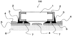
- FIG. 1 is a cross-sectional view illustrating a main part of the electronic control device 100 according to the first embodiment.
- the electrode 2 of the electronic component 1 and the conductor 5 (wiring) of the circuit board 6 are connected by the conductive bonding material 3.
- the electronic component 1 has, for example, a chip resistance 3216 size (3.2 mm ⁇ 1.6 mm), and the conductive bonding material 3 uses solder.
- the chip resistor shown in FIG. 1 is a leadless chip component.
- the circuit board 6 is a printed board, and includes a solder resist 4 and a conductor 5 for protecting wiring, and a non-metallic member 7 in a region (electrode pad) to which the solder of the conductor 5 is connected.
- the non-metallic member 7 is made of the same material as that of the solder resist 4, and in the electronic control device 100, the non-metallic member 7 exists between the electrode 2 of the electronic component 1 and the conductor 5 facing the solder.
- the electronic component 1 has an electrode 2, and the circuit board 6 has a conductor 5 that faces the electrode 2.
- the conductive bonding material 3 bonds the electrode 2 and the conductor 5 together.
- the nonmetallic member 7 (insulating member) is disposed in the conductive bonding material 3 and is in contact with the conductor 5 and the electrode 2. That is, the nonmetallic member 7 has a height in the direction connecting the electrode 2 and the conductor 5, and protrudes from the conductor 5 toward the electrode 2.
- the height from the surface of the conductor 5 (a 1st conductor and a 2nd conductor) of the two nonmetallic members 7 (a 1st insulating member and a 2nd insulating member) shown in FIG. 1 is the same. is there.
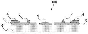
- FIG. 2 is a top view of the circuit board 6 before the electronic component 1 is mounted
- FIG. 3 is a cross-sectional view taken along the line X-X ′ of FIG.
- the nonmetallic member 7 is disposed on the conductor 5 to which the electronic component 1 is soldered.
- the non-metallic member 7 is the same material as the solder resist 4 applied as a protective film on the surface layer of the circuit board 6.
- the non-metallic member 7 (insulating member) is made of the same material as the solder resist 4 that protects the circuit board 6.
- the nonmetallic member 7 is separated from the solder resist 4 that protects the circuit board 6 and is isolated.
- the two non-metallic members 7 (the first insulating member and the second insulating member) are arranged in the arrangement direction of the two conductors 5 (the first conductor and the second conductor). Arranged in a row.
- the electronic control device 100 of this embodiment can be manufactured in the same process as the manufacturing process of the conventional printed circuit board and the electronic control device.
- the non-metallic member 7 that is a feature of the first embodiment is formed in an existing manufacturing process of “solder resist coating / exposure / development” in the printed circuit board manufacturing process.
- a solder resist is applied to the entire surface of the substrate by, for example, a spray method or a printing method (S10). Thereafter, in the “exposure” step, the portion where the solder resist is to be formed is cured by exposure using a photomask (S15). At this time, the solder resist is hardened in the soldering region of the conductor 5. In the next “development” step, the uncured portion that does not require the solder resist is washed away (S20).
- the non-metal member 7 formed as a result is a cylinder having a diameter of 0.1 mm, for example.
- the columnar non-metallic member 7 (insulating member) is formed on the conductor 5 of the circuit board 6 in the steps S10 to S20.
- a film-like solder resist 4 for protecting the circuit board 6 is also formed. That is, the columnar non-metallic member 7 is formed as a solder resist in the step of forming the solder resist 4 that protects the circuit board 6.
- the electronic component 1 is soldered to the circuit board 6 which is a manufacturing process of the electronic control device 100. This is the same as the conventional process, and a solder paste is printed on the conductor 5 of the substrate using a solder mask (S25). Thereafter, the electronic component 1 is mounted and the solder is cured in the reflow process (S30).
- the conductive bonding material 3 is disposed on the columnar non-metallic member 7 (insulating member) in the step S25, and the electronic component 1 is disposed on the conductive bonding material 3 in the step S30. Then, the electrode 2 of the electronic component 1 and the conductor 5 of the circuit board 6 are joined by the conductive joining material 3.
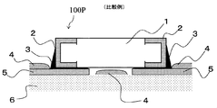
- FIG. 4 is a cross-sectional view showing an electronic control device 100P, which is a comparative example with the first embodiment.
- the electrode 2 of the electronic component 1 and the conductor 5 of the circuit board 6 are connected by the conductive bonding material 3, but the volume of the conductive bonding material 3 between the electronic component 1 and the conductor 5 is extremely small.
- the distance between the electrode 2 and the opposing conductor 5, that is, the connection height of the solder is about 10 ⁇ m, and in some cases, it may be substantially equal to zero. This is due to the weight of the electronic component 1, and the electronic component sinks into the molten solder during reflow, and the solder is cured as it is.
- FIG. 5 is a graph showing the relationship between the solder connection height and the solder thermal fatigue life.
- the solder connection height H affects the fatigue life Nf of the solder accompanying a change in temperature.
- the nonmetallic member 7 functions as a spacer when the electronic component 1 is mounted on the solder paste printed on the conductor 5 due to the presence of the nonmetallic member 7 disposed on the conductor 5 of the circuit board 6. Fulfill.
- the volume of the solder between the electronic component 1 and the conductor 5 is kept constant without the electronic component 1 sinking into the molten solder. That is, it is possible to keep the solder connection height higher than before and keep it constant.
- non-metallic member 7 is present in a form encased in solder, there is no fear of causing breakage starting from the non-metallic member such as peeling between the non-metallic member 7 and the conductor 5.
- the present embodiment provides an electronic control device with improved reliability without incurring a cost increase that can be realized only by existing processes.
- the graph of the relationship between the solder connection height H and the solder thermal fatigue life Nf shown in FIG. 5 also shows the relationship between the voids in the solder and the fatigue life. As can be seen from the graph, the fatigue life Nf of the solder decreases as the number of voids in the solder increases.
- the nonmetallic member 7 shown in FIGS. 1, 2, and 3 is a member having an electric resistance of 1 ⁇ 10 3 ⁇ or more. Due to the presence of the non-metallic member 7, voids in the solder can be reduced as will be described below.
- the non-metallic member 7 is made of a material having an electrical resistivity of 1 ⁇ 10 3 or more, thereby reducing voids in the solder after soldering and extending the fatigue life of the solder. Is possible. As a result, an electronic control device with improved reliability is realized.
- the height of the conductive bonding material 3 (solder) between the electrode 2 of the electronic component 1 and the conductor 5 of the circuit board 6 is secured by the non-metallic member 7, so that the fatigue life of the conductive bonding material 3 is maintained. Can be improved. Further, since the nonmetallic member 7 has insulating properties and lower wettability than the metal, an alloy layer is not formed at the boundary between the nonmetallic member 7 and the conductive bonding material 3, and convection occurs when the conductive bonding material 3 is melted. Is prone to occur. As a result, voids can be reduced.
- the non-metallic member 7 has a height in a direction connecting the electrode 2 of the electronic component 1 and the opposing conductor 5, and the height is 10 ⁇ m or more. In other words, the height of the nonmetallic member 7 (insulating member) from the surface of the conductor 5 is 10 ⁇ m or more.
- the non-metallic member 7 shown in FIGS. 1, 2, and 3 is a solder resist having a height of 30 ⁇ m. Moreover, it is set as a cylindrical shape with a diameter of 0.1 mm.
- the solder resist on the surface layer of the circuit board 6 generally has a thickness of 25 ⁇ m to 50 ⁇ m and a minimum coating width of 0.1 mm. Therefore, the nonmetallic member 7 can be formed only by the existing solder resist coating process in the manufacturing process of the circuit board 6.
- the thickness is smaller than the general thickness (100 to 150 ⁇ m) of the solder printing mask used in the solder printing process. Soldering can be performed in the same process as existing, without jumping out of the solder printing mask. As a result, an electronic control device with improved solder connection reliability can be obtained.
- the height of the conductive bonding material 3 for bonding the electrode 2 of the electronic component 1 and the conductor 5 of the circuit board 6 is secured, and the inside of the conductive bonding material 3 is secured. Voids can be reduced. As a result, the connection reliability of the conductive bonding material 3 is improved.
- the nonmetallic member 7 can be formed only by the existing solder resist coating process in the manufacturing process of the circuit board 6, the manufacturing cost can be reduced.
- FIG. 6 is a cross-sectional view showing a main part of the electronic control device 100 of the second embodiment.
- two nonmetallic members 7 are provided in the conductive bonding material 3 at a pair of bonding portions 8 and 9 between the electrode 2 of the electronic component 1 and the conductor 5 of the circuit board 6 facing each other.
- all the non-metallic members 7 are formed to have the same height.
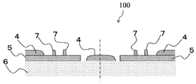
- FIG. 7 is a top view of the circuit board 6, and FIG. 8 is a cross-sectional view taken along the line Y-Y 'of FIG.
- the joining portion 8 and the nonmetallic member 7 of the joining portion 9 are formed so as to be positioned symmetrically with respect to the center of the electronic component 1. That is, the nonmetallic member 7 (insulating member) is disposed symmetrically with respect to a plane that passes through the center of the electronic component 1 and is perpendicular to the arrangement direction of the electrodes 2 of the electronic component 1.
- all the non-metallic members 7 are arranged in the direction in which the two conductors 5 (first conductor and second conductor) are arranged. Arranged in a row.
- the non-metallic member 7 provided at each joint is symmetrical with respect to the center of the electronic component 1, when the electronic component 1 is mounted on the conductor 5 of the circuit board 6 and joined, The electronic component 1 is prevented from tilting. As a result, it is possible to obtain an electronic control device that increases the solder connection height without tilting the electronic component 1 and improves the solder connection reliability.
- thermosetting organic solvent is used for the non-metallic member 7 for example.
- S40 to S50 are the same as S10 to S20 of FIG. 10 except for the formation of the non-metallic member 7, and thus description thereof is omitted.
- thermosetting organic solvent is applied to the conductor 5 of the circuit board 6 in a columnar shape using, for example, a cylinder (S55).
- the non-metallic member 7 is formed by curing the organic solvent in an environment of the curing temperature of the organic solvent (S60).
- the conductive bonding material 3 of the circuit board 6 is applied by, for example, mask printing (S65).
- the electronic component 1 is mounted on the upper surface, and the electrode 2 of the electronic component 1, the conductive bonding material 3, and the conductor 5 are bonded by passing through the environment of the curing temperature of the conductive bonding material 3 (S ⁇ b> 70). ).
- the nonmetallic member 7 even when the nonmetallic member 7 is not formed in advance in the circuit board manufacturing process, it is possible to form the nonmetallic member 7 by adding a process before mounting the electronic component. As a result, it is possible to obtain an electronic control device that achieves a structure in which the solder connection height is increased and the voids in the solder are reduced, and the reliability is improved.
- the present invention is not limited to the above-described embodiment, and includes various modifications.
- the above-described embodiment has been described in detail for easy understanding of the present invention, and is not necessarily limited to the one having all the configurations described.
- a part of the configuration of an embodiment can be replaced with the configuration of another embodiment, and the configuration of another embodiment can be added to the configuration of an embodiment.
- the non-metallic member 7 (insulating member) is cylindrical, but may be prismatic. Moreover, the non-metallic member 7 may have a pillow shape (bank shape).
- the electronic component 1 may have two or more electrodes 2, and the circuit board 6 may have two or more conductors 5 respectively facing the electrodes 2.
- an electronic control device including a circuit board on which an electronic component is mounted, the electrode and the conductor are included in a conductive bonding material that joins an electrode of the electronic component and a conductor of the circuit board.
- An electronic control device in which a non-metallic member having a height in the direction of tying is disposed.
- the non-metallic member has a pair of electrodes facing each other along a planar direction of the circuit board, and the non-metallic member is formed of each conductive bonding material that joins the pair of electrodes and the conductor.
- the solder connection reliability is improved by controlling the solder connection height to be constant. And it can be realized only by existing processes.
- Patent Document 1 a solder paste for adjusting the solder connection height is used separately from the solder paste for connecting the electronic component and the electrode of the substrate.
- the solder paste for adjusting the solder height is partially applied on the solder resist on the board surface, and rises and collects on the land due to the surface tension of the solder melted at the time of reflow. Adjust. That is, the invention is an invention in which the solder connection height is controlled by the weight of the electronic component and the volume of the height adjusting solder paste.
- the scaffold of the electronic component mounted on the solder paste is an unstable molten solder at the time of reflow, and there is a concern that the electronic component is inclined and connected. Therefore, with the technology of Patent Document 1, it may be difficult to control the height to be constant without tilting the electronic component.
- Patent Document 2 relates to a structure for joining an electronic component to a substrate using solder balls.
- a metal core in the solder ball By providing a metal core in the solder ball, the solder connection height after reflowing is ensured to a certain level, and the solder connection reliability can be improved.
- Patent Document 2 requires a new manufacturing process for manufacturing a solder ball with a built-in metal core. The technique of Patent Document 2 is applied only to a structure using solder balls such as BGA (Ball Grid Array) or flip chip.
- BGA Ball Grid Array
Landscapes
- Engineering & Computer Science (AREA)
- Manufacturing & Machinery (AREA)
- Microelectronics & Electronic Packaging (AREA)
- Electric Connection Of Electric Components To Printed Circuits (AREA)
Abstract
電子部品の電極と回路基板の導体を接合する導電性接合材の高さを確保しつつ、導電性接合材の内部のボイドを低減することができる電子回路装置及び方法を提供する。電子制御装置100(電子回路装置)は、電子部品1と、回路基板6と、導電性接合材3と、非金属部材7(絶縁性部材)と、を備える。電子部品1は、電極2を有し、回路基板6は、電極2に対向する導体5を有する。導電性接合材3は、電極2と導体5とを接合する。非金属部材7(絶縁性部材)は、導電性接合材3の中に配置され、導体5と電極2に接する。
Description
本発明は、電子回路装置及び方法に関する。
電子制御装置(電子回路装置)の小型化・高密度実装化、また、高温環境下への搭載位置の変更により、電子制御装置の高寿命化が要求されている。電子制御装置の製品寿命を決定する1つのファクタとして、はんだ接続部の寿命がある。
電子部品と基板のはんだ接続部には、温度変化の環境下において、電子部品と基板の線膨張係数差に起因した応力が発生する。温度変化によって発生する応力が、繰り返しかかることではんだにはせん断ひずみが生じ、やがて破壊に至る。この繰り返し応力によってはんだに生じる破壊を熱疲労破壊と呼び、熱疲労破壊によって破断に至るまでの寿命を熱疲労破壊寿命と呼ぶ。
はんだの熱疲労破壊を抑制するための策として、はんだの接続高さのコントロールがある。はんだの接続高さが低い程、はんだ接続部に発生するせん断ひずみは拡大し、熱疲労破壊寿命は短寿命となる。一方、はんだ接続高さが高いとはんだ接続部に発生するせん断ひずみは縮小し、熱疲労破壊寿命は長寿命となる。
電子部品と基板のはんだ接続部の接続高さを稼ぐことではんだの熱疲労寿命を向上させる技術が開示されている(例えば、特許文献1参照)。この特許文献1には、「実装面の対向領域内にリード端子に接続されない未接続ランドの少なくとも一部が配置され、この未接続ランド上に半導体装置における本体部の下面に接触する高さ調整用はんだは、一部がソルダーレジスト上に配置されるはんだペーストが、リフロー処理時に溶融し表面張力により未接続ランド上に集まって盛り上がるように形成されることで、本体部の下面に対して押し上げるように接触する。」と記載されている。
また、同様に、はんだの接続高さを稼ぐことによりはんだ接続部の長期接続信頼性を向上させる技術が開示されている(例えば、特許文献2参照)。この特許文献2には、「半導体素子の電極パッドと基板上の電極パッドとをはんだボールによって接続する。はんだボールは、金属製コア部と、金属製コア部の周囲に設けられ、前記コア部よりも剛性が低く融点が低いはんだ部とで構成されている。はんだボールを半導体素子にリフローによって接続する。その後、はんだボールが付いた半導体素子と基板を超音波にて接続し、基板側において金属コアと電極を直接接続する。」と記載されている。
特許文献1及び2に開示されるような技術によれば、電子部品の電極と回路基板の導体を接合するはんだ(導電性接合材)の高さを確保することができる。
一方、はんだの内部に発生するボイドによりはんだの接続信頼性が低下するという問題が知られている。
本発明の目的は、電子部品の電極と回路基板の導体を接合する導電性接合材の高さを確保しつつ、導電性接合材の内部のボイドを低減することができる電子回路装置及び方法を提供することにある。
上記目的を達成するために、本発明は、電極を有する電子部品と、前記電極に対向する導体を有する回路基板と、前記電極と前記導体とを接合する導電性接合材と、前記導電性接合材の中に配置され、前記導体と前記電極に接する絶縁性部材と、を備える。
本発明によれば、電子部品の電極と回路基板の導体を接合する導電性接合材の高さを確保しつつ、導電性接合材の内部のボイドを低減することができる。上記した以外の課題、構成及び効果は、以下の実施形態の説明により明らかにされる。
以下、図面を用いて、本発明の第1~第2の実施形態に関わる電子制御装置の構成及び製造方法について説明する。なお、各図において、同一符号は同一部分を示す。
(全体構成)
初めに、図9を用いて、電子制御装置100(電子回路装置)の全体構成を説明する。図9は、本発明の第1~第2の実施形態に関わる電子制御装置100の一例を示す断面図である。
初めに、図9を用いて、電子制御装置100(電子回路装置)の全体構成を説明する。図9は、本発明の第1~第2の実施形態に関わる電子制御装置100の一例を示す断面図である。
電子制御装置100は、主として、カバー31、ベース32、コネクタ21、回路基板6を備える。なお、カバー31及びベース32は、筐体を構成し、回路基板6を収容する。
図9では、電子部品1及び半導体パッケージ11(電子部品)は、導電性接合材3を介して回路基板6に電気的に接続されている。コネクタ21は、回路基板6に接続されるコネクタ端子22を有し、外部コネクタと嵌合する。カバー31とコネクタ21の間、カバー31とベース32の間、コネクタ21とベース32の間は、シール材41でシールされている。
ベース32は、半導体パッケージ11へ向けて突出するボス32aを有する。半導体パッケージ11が搭載される回路基板6の面(表面)と反対側の面(裏面)と、ボス32aの先端側の面との間には、放熱部材42が配置される。
(第1の実施形態)
図1は第1の実施形態の電子制御装置100の要部を示す断面図である。電子部品1の電極2と回路基板6の導体5(配線)とが導電性接合材3により接続されている。ここで、電子部品1は、例えばチップ抵抗3216サイズ(3.2mm×1.6mm)とし、導電性接合材3にははんだを用いる。なお、図1に示すチップ抵抗は、リードレスなチップ部品である。
図1は第1の実施形態の電子制御装置100の要部を示す断面図である。電子部品1の電極2と回路基板6の導体5(配線)とが導電性接合材3により接続されている。ここで、電子部品1は、例えばチップ抵抗3216サイズ(3.2mm×1.6mm)とし、導電性接合材3にははんだを用いる。なお、図1に示すチップ抵抗は、リードレスなチップ部品である。
また、回路基板6はプリント基板とし、配線を保護するためのソルダーレジスト4および導体5を備え、導体5のはんだが接続される領域(電極パッド)に非金属部材7を備えた基板である。非金属部材7は、ソルダーレジスト4と同一の材料とし、電子制御装置100においては電子部品1の電極2と相対する導体5の間にはんだに覆われるかたちで存在する。
換言すれば、図1に示すように、電子部品1は、電極2を有し、回路基板6は、電極2に対向する導体5を有する。導電性接合材3は、電極2と導体5とを接合する。非金属部材7(絶縁性部材)は、導電性接合材3の中に配置され、導体5と電極2に接する。つまり、非金属部材7は、電極2と導体5とを結ぶ方向に高さを有し、導体5から電極2へ向けて突出する。なお、図1に示す2つの非金属部材7(第1の絶縁性部材と第2の絶縁性部材)の導体5(第1の導体と第2の導体)の表面からの高さは同じである。
図2は電子部品1実装前の回路基板6の上面図、図3は図2のX-X’断面図である。図1で説明した通り、電子部品1がはんだ付けされる導体5上に、非金属部材7を配置している。非金属部材7は回路基板6の表層の保護膜として塗布するソルダーレジスト4と同一の材料である。
換言すれば、非金属部材7(絶縁性部材)は、回路基板6を保護するソルダーレジスト4と同じ材料でできている。非金属部材7は、回路基板6を保護するソルダーレジスト4と分離され、孤立している。図2に示すように、2つの非金属部材7(第1の絶縁性部材と前記第2の絶縁性部材)は、2つの導体5(第1の導体と第2の導体)の配列方向に一列に配置される。
(第1の製造方法)
次に、図10を用いて、第1の実施形態の電子制御装置100の製造工程について説明する。本実施形態の電子制御装置100は、従来のプリント基板および電子制御装置の製造工程と同一の工程で製造できる。第1の実施形態の特徴である非金属部材7は、一例として、プリント基板製造工程の「ソルダーレジスト塗布・露光・現像」の既存の製造工程において形成する。
次に、図10を用いて、第1の実施形態の電子制御装置100の製造工程について説明する。本実施形態の電子制御装置100は、従来のプリント基板および電子制御装置の製造工程と同一の工程で製造できる。第1の実施形態の特徴である非金属部材7は、一例として、プリント基板製造工程の「ソルダーレジスト塗布・露光・現像」の既存の製造工程において形成する。
具体的には、ソルダーレジストを例えばスプレー方式あるいは印刷方式等により基板全面に塗布する(S10)。その後、「露光」工程において、ソルダーレジストを形成する部分をフォトマスクを用いて露光により硬化する(S15)。この時に、導体5のはんだ付け領域にソルダーレジストを硬化させる。次の「現像」工程において、ソルダーレジストの不要となる未硬化部分を洗い流す(S20)。この結果形成した非金属部材7は、例えばφ0.1mmの円柱とする。
換言すれば、S10~S20の工程において、回路基板6の導体5の上に柱状の非金属部材7(絶縁性部材)が形成される。S10~S20の工程では、回路基板6を保護する膜状のソルダーレジスト4も形成される。つまり、柱状の非金属部材7は、回路基板6を保護するソルダーレジスト4を形成する工程において、ソルダーレジストとして形成される。
次に電子制御装置100の製造工程である回路基板6に電子部品1をはんだ付けする工程である。従来の工程と同一であり、はんだマスクを用いて基板の導体5にはんだペーストを印刷する(S25)。その後、電子部品1を搭載しリフロー工程においてはんだを硬化させる(S30)。
換言すれば、S25の工程において、柱状の非金属部材7(絶縁性部材)の上に導電性接合材3を配置し、S30の工程において、導電性接合材3の上に電子部品1を配置し、電子部品1の電極2と回路基板6の導体5とを導電性接合材3で接合する。
一方、図4は、第1の実施形態との比較例である電子制御装置100Pを示す断面図である。電子部品1の電極2と回路基板6の導体5とが導電性接合材3により接続されているが、電子部品1と導体5との間の導電性接合材3の体積は極めて少ない。電極2と対向する導体5との間の距離、即ちはんだの接続高さは約10μm程度、場合によってはほぼ0に等しいこともある。これは、電子部品1の自重に因るものであり、リフロー時に電子部品が溶融したはんだ内に沈み込んでしまい、そのままはんだが硬化するためである。
図5は、はんだの接続高さとはんだの熱疲労寿命の関係を示したグラフである。はんだの接続高さHは、温度変化に伴うはんだの疲労寿命Nfに影響し、はんだの接続高さHが低い程、疲労寿命Nfは短くなる(小さくなる)。
本実施形態によれば、回路基板6の導体5に配置した非金属部材7の存在により、電子部品1を導体5に印刷したはんだペースト上に搭載した際に、非金属部材7がスペーサーの役目を果たす。この結果、電子部品1が溶融はんだ内に沈み込むことなく、電子部品1と導体5との間のはんだの体積を一定量に保つ。つまり、はんだの接続高さを従来よりも高くし一定に保つことが可能となる。
また、非金属部材7ははんだに包まれた形で存在するため、非金属部材7と導体5との間の剥離など非金属部材を起点とした破壊が生じる心配はない。
以上、本実施形態は、既存の工程のみで実現可能なコストアップを招く事の無い信頼性を向上させた電子制御装置を提供する。
次に非金属部材7の存在によるはんだ内ボイドへの影響について説明する。図5に示したはんだの接続高さHとはんだの熱疲労寿命Nfの関係のグラフは、はんだ内のボイドと疲労寿命の関係も示す。グラフから判るように、はんだ内のボイドが多い程はんだの疲労寿命Nfは低下する。
図1、2、3に示した非金属部材7は、電気抵抗が1×10³Ω以上の部材とする。この非金属部材7の存在により、以下に示すように、はんだ内のボイドを低減することが可能である。
ボイド発生と消失の工程について説明する。リフロー工程でのはんだ溶融時に、はんだ内にはんだとは異なる非金属部材7が存在することにより、溶融はんだの対流が活発に起きる。対流が活発に起きることにより、溶融はんだ内に存在するフラックスや気泡が溶融はんだの外部へ抜け出ていき易い状態となる。
本実施形態によれば、非金属部材7を電気抵抗率が1×10³以上の材料とすることにより、はんだ付け後のはんだ内のボイドを低減し、はんだの疲労寿命を長寿命化することが可能となる。この結果、信頼性を向上させた電子制御装置を実現する。
このように、非金属部材7により電子部品1の電極2と回路基板6の導体5の間の導電性接合材3(はんだ)の高さが確保されるため、導電性接合材3の疲労寿命を向上することができる。また、非金属部材7は絶縁性を有するとともに濡れ性が金属よりも低いため、非金属部材7と導電性接合材3の境界で合金層が形成されず、導電性接合材3の溶融時に対流が起きやすい。その結果、ボイドを低減することができる。
次に、非金属部材7のサイズについて説明する。非金属部材7は、電子部品1の電極2と、相対する導体5とを結ぶ方向に高さを有し、該高さは10μm以上とする。換言すれば、導体5の表面からの非金属部材7(絶縁性部材)の高さは、10μm以上である。
例えば、図1、2、3で示した非金属部材7は高さ30μmのソルダーレジストとする。また、直径0.1mmの円柱状とする。回路基板6の表層のソルダーレジストは、一般に厚み25μm~50μm、最少塗布幅は0.1mmとされている。よって、非金属部材7は回路基板6の製造工程における既存のソルダーレジスト塗布工程のみにより形成することが可能である。
加えて、非金属部材7の高さを30μmとする場合、該厚みは、はんだ印刷工程において使用するはんだ印刷マスクの一般的な厚み(100~150μm)よりも小さいため、はんだ印刷時に非金属部材7がはんだ印刷マスクから飛び出る事無く、既存と変わりない工程ではんだ付けを実施できる。この結果、はんだの接続信頼性を向上させた電子制御装置を得ることが可能となる。
以上説明したように、本実施形態によれば、電子部品1の電極2と回路基板6の導体5を接合する導電性接合材3の高さを確保しつつ、導電性接合材3の内部のボイドを低減することができる。その結果、導電性接合材3の接続信頼性が向上する。
また、非金属部材7を回路基板6の製造工程における既存のソルダーレジスト塗布工程のみにより形成することができるため、製造コストを低減することができる。
(第2の実施形態)
次に、図6~図8を用いて、第1の実施形態と異なる非金属部材の構成(配置)について説明する。
次に、図6~図8を用いて、第1の実施形態と異なる非金属部材の構成(配置)について説明する。
図6は第2の実施形態の電子制御装置100の要部を示す断面図である。本構造では、電子部品1の電極2と相対する回路基板6の導体5との1対の接合部8、9において、導電性接合材3の中に非金属部材7をそれぞれ2つ設けている。また、全ての非金属部材7の高さは同一となるよう形成する。
図7は回路基板6の上面図、図8は図7のY-Y’断面図を示している。接合部8および接合部9の非金属部材7は、電子部品1の中心に対して対称に位置するよう形成している。すなわち、非金属部材7(絶縁性部材)は、電子部品1の中心を通り電子部品1の電極2の配列方向に垂直な平面に対して対称に配置される。
また、図7に示すように、全ての非金属部材7(第1の絶縁性部材~第4の絶縁性部材)は、2つの導体5(第1の導体と第2の導体)の配列方向に一列に配置される。
本実施形態によれば、各接合部に設けた非金属部材7が電子部品1の中心に対して対称であることから、電子部品1を回路基板6の導体5に搭載し接合する際に、電子部品1が傾くことを防ぐ。この結果、電子部品1が傾くことなくはんだの接続高さを稼ぎ、はんだの接続信頼性を向上させた電子制御装置を得ることが可能となる。
(第2の製造方法)
既存の工程に新たに工程を追加し非金属部材7を形成する方法を説明する。
既存の工程に新たに工程を追加し非金属部材7を形成する方法を説明する。
図1および図6にて示す非金属部材7を、回路基板製造後、部品搭載前に工程を加えることで形成する。非金属部材7には、例えば、熱硬化性の有機溶剤を用いる。
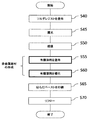
図11を用いて、本実施形態の製造工程について説明する。なお、図11において、S40~S50は、非金属部材7の形成を除き、図10のS10~S20と同じであるため、説明を省略する。
S50に続いて、回路基板6の導体5上に熱硬化性の有機溶剤を、例えばシリンダーを用い柱状に塗布する(S55)。次に、該有機溶剤の硬化温度の環境で有機溶剤を硬化させることにより非金属部材7を形成する(S60)。その後、回路基板6の導電性接合材3を例えばマスク印刷により塗布する(S65)。リフロー工程において、その上面に電子部品1を搭載し、導電性接合材3の硬化温度の環境に通すことにより、電子部品1の電極2と導電性接合材3と導体5とを接合する(S70)。
本実施形態によれば、非金属部材7を予め回路基板製造工程にて形成していない場合でも、電子部品搭載前に工程を追加することで非金属部材7を形成することが可能である。その結果、はんだの接続高さを稼ぎ、且つはんだ内ボイドを低減させた構造を実現し、信頼性を向上させた電子制御装置を得ることが可能である。
なお、本発明は上記した実施形態に限定されるものではなく、様々な変形例が含まれる。例えば、上述した実施形態は本発明を分かりやすく説明するために詳細に説明したものであり、必ずしも説明した全ての構成を備えるものに限定されるものではない。また、ある実施形態の構成の一部を他の実施形態の構成に置き換えることが可能であり、また、ある実施形態の構成に他の実施形態の構成を加えることも可能である。また、各実施形態の構成の一部について、他の構成の追加・削除・置換をすることが可能である。
上記実施形態では、非金属部材7(絶縁性部材)は円柱状であるが、角柱状であってもよい。また、非金属部材7は、まくら木状(堤状)であってもよい。
また、電子部品1は2つ以上の電極2を有し、回路基板6はこれらの電極2にそれぞれ対向する2つ以上の導体5を有するようにしてもよい。
なお、本発明の実施形態は、以下の態様であってもよい。
(1)電子部品が実装される回路基板を備える電子制御装置において、前記電子部品が有する電極と、前記回路基板の導体とを接合する導電性接合材の中に、前記電極と前記導体とを結ぶ方向に高さを有する非金属部材が配置される、電子制御装置。
(2)前記非金属部材は、前記回路基板の表層に施されるソルダーレジストによって構成される、(1)に記載の電子処理装置。
(3)前記回路基板の導体に配置される前記非金属部材としてのソルダーレジストは、前記回路基板の表層に施されるソルダーレジストとは分離して形成される、(2)に記載の電子制御装置。
(4)前記非金属部材は、電気抵抗が103Ω以上である、(1)に記載の電子制御装置。
(5)前記非金属部材は、高さが10μm以上である、(1)に記載の電子制御装置。
(6)前記非金属部材は、前記方向の延びる柱形状を有する、(1)に記載の電子制御装置。
(7)前記非金属部材は、前記回路基板の平面方向に沿って対向する一対の電極を有し、前記非金属部材は、前記一対の電極と前記導体とを接合する各導電性接合材の中にそれぞれ配置され、前記各非金属部材は、高さが同一である、(1)に記載の電子制御装置。
(1)~(7)の実施形態によれば、電子部品をはんだにより基板のランドに接続する電子制御装置において、はんだの接続高さを一定にコントロールすることによりはんだの接続信頼性を向上させ、且つそれは既存の工程のみで実現させることができる。
特許文献1では、電子部品と基板の電極を接続するためのはんだペーストとは別に、はんだ接続高さを調節するためのはんだペーストを用いている。該はんだ高さ調節用のはんだペーストは、一部が基板表面のソルダーレジスト上に塗布され、リフロー時に溶融したはんだの表面張力によってランド上に盛り上がって集まることで電子部品と基板のはんだ接続高さを調節する。つまり、電子部品の重さと高さ調節用はんだペーストの体積によってはんだ接続高さをコントロールしようという発明である。しかし、はんだペーストの上に搭載された電子部品の足場は、リフロー時には不安定な溶融はんだとなっており、電子部品が傾いて接続されることが懸念される。よって、特許文献1の技術では電子部品が傾くことなく高さを一定にコントロールすることが困難となる可能性がある。
これに対し、上記実施形態によれば、電子部品が傾くことなく高さを一定にコントロールすることが容易である。
特許文献2は、はんだボールを用いて電子部品を基板に接合する構造に関する。はんだボール内に金属コアを設けることによりリフロー後のはんだ接続高さを一定の高さに確保し、はんだ接続信頼性を向上させることを可能としている。しかし、特許文献2では、金属コアを内蔵したはんだボールを製造するための新たな製造プロセスが必要となる。また、特許文献2の技術は、BGA(Ball Grid Array)やフリップチップ等のはんだボールを用いた構造のみに適用するものである。
これに対し、上記実施形態によれば、任意の電子部品に適用することができる。
1…電子部品
2…電子部品の電極
3…導電性接合材
4…ソルダーレジスト
5…導体
6…回路基板
7…非金属部材
8…電極2と導電性接合材3と導体5との接合部
9…電極2と導電性接合材3と導体5との接合部
11…半導体パッケージ
21…コネクタ
22…コネクタ端子
31…カバー
32…ベース
32a…ボス
41…シール材
42…放熱部材
100、100P…電子制御装置
2…電子部品の電極
3…導電性接合材
4…ソルダーレジスト
5…導体
6…回路基板
7…非金属部材
8…電極2と導電性接合材3と導体5との接合部
9…電極2と導電性接合材3と導体5との接合部
11…半導体パッケージ
21…コネクタ
22…コネクタ端子
31…カバー
32…ベース
32a…ボス
41…シール材
42…放熱部材
100、100P…電子制御装置
Claims (11)
- 電極を有する電子部品と、
前記電極に対向する導体を有する回路基板と、
前記電極と前記導体とを接合する導電性接合材と、
前記導電性接合材の中に配置され、前記導体と前記電極に接する絶縁性部材と、
を備えることを特徴とする電子回路装置。 - 請求項1に記載の電子回路装置であって、
前記絶縁性部材は、
前記回路基板を保護するソルダーレジストと同じ材料でできている
ことを特徴とする電子回路装置。 - 請求項2に記載の電子回路装置であって、
前記絶縁性部材は、
前記回路基板を保護するソルダーレジストと分離される
ことを特徴とする電子回路装置。 - 請求項1に記載の電子回路装置であって、
前記絶縁性部材の電気抵抗は、
103Ω以上である
ことを特徴とする電子回路装置。 - 請求項1に記載の電子回路装置であって、
前記導体の表面からの前記絶縁性部材の高さは、
10μm以上である
ことを特徴とする電子回路装置。 - 請求項1に記載の電子回路装置であって、
前記絶縁性部材は、
柱状である
ことを特徴とする電子回路装置。 - 請求項1に記載の電子回路装置であって、
前記電極は、
少なくとも第1の電極と第2の電極から構成され、
前記導体は、
少なくとも第1の導体と第2の導体から構成され、
前記導電性接合材は、
前記第1の電極と前記第1の導体とを接合する第1の導電性接合材と、
前記第2の電極と前記第2の導体とを接合する第2の導電性接合材と、を含み、
前記絶縁性部材は、
前記第1の導電性接合材の中に配置され、前記第1の導体と前記第1の電極に接する第1の絶縁性部材と、
前記第2の導電性接合材の中に配置され、前記第2の導体と前記第2の電極に接する第2の絶縁性部材と、を含み、
前記第1の導体の表面からの前記第1の絶縁性部材の高さは、
前記第2の導体の表面からの前記第2の絶縁性部材の高さと同じである
ことを特徴とする電子回路装置。 - 請求項7に記載の電子回路装置であって、
前記第1の絶縁性部材と前記第2の絶縁性部材は、
前記第1の導体と前記第2の導体の配列方向に一列に配置される
ことを特徴とする電子回路装置。 - 請求項7に記載の電子回路装置であって、
前記絶縁性部材は、
前記第1の導電性接合材の中に配置され、前記第1の導体と前記第1の電極に接する第3の絶縁性部材と、
前記第2の導電性接合材の中に配置され、前記第2の導体と前記第2の電極に接する第4の絶縁性部材と、をさらに含み、
前記第1の絶縁性部材~前記第4の絶縁性部材の高さは、同じであり、
前記第1の導体と前記第2の導体の配列方向に一列に配置される
ことを特徴とする電子回路装置。 - 回路基板の導体の上に柱状の絶縁性部材を形成する工程と、
柱状の前記絶縁性部材の上に導電性接合材を配置する工程と、
前記導電性接合材の上に電子部品を配置する工程と、
前記電子部品の電極と前記回路基板の前記導体とを前記導電性接合材で接合する工程と、
を有することを特徴とする方法。 - 請求項10に記載の方法であって、
前記回路基板を保護するソルダーレジストを形成する工程をさらに有し、
柱状の前記絶縁性部材は、
前記回路基板を保護するソルダーレジストを形成する工程において、ソルダーレジストとして形成される
ことを特徴とする方法。
Priority Applications (1)
| Application Number | Priority Date | Filing Date | Title |
|---|---|---|---|
| JP2018519131A JPWO2017203859A1 (ja) | 2016-05-25 | 2017-04-11 | 電子回路装置及び方法 |
Applications Claiming Priority (2)
| Application Number | Priority Date | Filing Date | Title |
|---|---|---|---|
| JP2016104213 | 2016-05-25 | ||
| JP2016-104213 | 2016-05-25 |
Publications (1)
| Publication Number | Publication Date |
|---|---|
| WO2017203859A1 true WO2017203859A1 (ja) | 2017-11-30 |
Family
ID=60411732
Family Applications (1)
| Application Number | Title | Priority Date | Filing Date |
|---|---|---|---|
| PCT/JP2017/014757 Ceased WO2017203859A1 (ja) | 2016-05-25 | 2017-04-11 | 電子回路装置及び方法 |
Country Status (2)
| Country | Link |
|---|---|
| JP (1) | JPWO2017203859A1 (ja) |
| WO (1) | WO2017203859A1 (ja) |
Cited By (2)
| Publication number | Priority date | Publication date | Assignee | Title |
|---|---|---|---|---|
| JP2019186329A (ja) * | 2018-04-05 | 2019-10-24 | 新光電気工業株式会社 | 配線基板、電子装置 |
| JP2022028391A (ja) * | 2020-08-03 | 2022-02-16 | 三菱電機エンジニアリング株式会社 | プリント基板、プリント基板の製造方法および電子部品の実装方法 |
Citations (5)
| Publication number | Priority date | Publication date | Assignee | Title |
|---|---|---|---|---|
| JPH08181419A (ja) * | 1994-12-22 | 1996-07-12 | Nissan Motor Co Ltd | プリント配線板の構造 |
| JP2000332394A (ja) * | 1999-05-24 | 2000-11-30 | Taiyo Yuden Co Ltd | 電子部品実装用基板及びその製造方法 |
| JP2011258794A (ja) * | 2010-06-10 | 2011-12-22 | Denso Corp | 電子装置およびその製造方法 |
| JP2012124397A (ja) * | 2010-12-10 | 2012-06-28 | Cmk Corp | 部品内蔵型多層プリント配線板 |
| JP2012165156A (ja) * | 2011-02-07 | 2012-08-30 | Nippon Dempa Kogyo Co Ltd | 発振器 |
Family Cites Families (2)
| Publication number | Priority date | Publication date | Assignee | Title |
|---|---|---|---|---|
| JP2008226946A (ja) * | 2007-03-09 | 2008-09-25 | Nec Corp | 半導体装置およびその製造方法 |
| WO2009157160A1 (ja) * | 2008-06-25 | 2009-12-30 | パナソニック株式会社 | 実装構造体、及び実装構造体の製造方法 |
-
2017
- 2017-04-11 JP JP2018519131A patent/JPWO2017203859A1/ja active Pending
- 2017-04-11 WO PCT/JP2017/014757 patent/WO2017203859A1/ja not_active Ceased
Patent Citations (5)
| Publication number | Priority date | Publication date | Assignee | Title |
|---|---|---|---|---|
| JPH08181419A (ja) * | 1994-12-22 | 1996-07-12 | Nissan Motor Co Ltd | プリント配線板の構造 |
| JP2000332394A (ja) * | 1999-05-24 | 2000-11-30 | Taiyo Yuden Co Ltd | 電子部品実装用基板及びその製造方法 |
| JP2011258794A (ja) * | 2010-06-10 | 2011-12-22 | Denso Corp | 電子装置およびその製造方法 |
| JP2012124397A (ja) * | 2010-12-10 | 2012-06-28 | Cmk Corp | 部品内蔵型多層プリント配線板 |
| JP2012165156A (ja) * | 2011-02-07 | 2012-08-30 | Nippon Dempa Kogyo Co Ltd | 発振器 |
Cited By (3)
| Publication number | Priority date | Publication date | Assignee | Title |
|---|---|---|---|---|
| JP2019186329A (ja) * | 2018-04-05 | 2019-10-24 | 新光電気工業株式会社 | 配線基板、電子装置 |
| JP7015721B2 (ja) | 2018-04-05 | 2022-02-03 | 新光電気工業株式会社 | 配線基板、電子装置 |
| JP2022028391A (ja) * | 2020-08-03 | 2022-02-16 | 三菱電機エンジニアリング株式会社 | プリント基板、プリント基板の製造方法および電子部品の実装方法 |
Also Published As
| Publication number | Publication date |
|---|---|
| JPWO2017203859A1 (ja) | 2019-02-14 |
Similar Documents
| Publication | Publication Date | Title |
|---|---|---|
| KR100921919B1 (ko) | 반도체 칩에 형성되는 구리기둥-주석범프 및 그의 형성방법 | |
| JP6206494B2 (ja) | 半導体装置 | |
| CN101145545A (zh) | 包括元件安装表面被树脂层涂覆的布线基板的半导体装置 | |
| US8810016B2 (en) | Semiconductor device, substrate and semiconductor device manufacturing method | |
| KR101054440B1 (ko) | 전자 소자 패키지 및 그 제조 방법 | |
| US20250183125A1 (en) | Electronic device and method for manufacturing electronic device | |
| JP2004266074A (ja) | 配線基板 | |
| US7928559B2 (en) | Semiconductor device, electronic component module, and method for manufacturing semiconductor device | |
| JP2019140179A (ja) | フリップチップ実装用の基板およびこれを用いた電子装置 | |
| JP2009105209A (ja) | 電子装置及びその製造方法 | |
| US20150144390A1 (en) | Wiring board and method for mounting semiconductor element on wiring board | |
| KR101101550B1 (ko) | 솔더 볼 및 반도체 패키지 | |
| JPWO2017203859A1 (ja) | 電子回路装置及び方法 | |
| US20100127382A1 (en) | Semiconductor device | |
| JP2010272563A (ja) | 部品内蔵配線板、部品内蔵配線板の製造方法 | |
| JP4952365B2 (ja) | 両面実装回路基板に対する電子部品の実装構造、半導体装置、及び両面実装半導体装置の製造方法 | |
| JP2004128290A (ja) | 半導体装置 | |
| JP5062376B1 (ja) | 電子部品実装基板の製造方法 | |
| JP4267549B2 (ja) | 半導体装置およびその製造方法ならびに電子機器 | |
| JP5369875B2 (ja) | 部品内蔵配線板、部品内蔵配線板の製造方法 | |
| JP2013211497A (ja) | 部品接合構造 | |
| JP2016162813A (ja) | プリント基板及びハンダ付け方法 | |
| JP5601413B2 (ja) | 部品内蔵配線板、部品内蔵配線板の製造方法 | |
| JP5577734B2 (ja) | 電子装置および電子装置の製造方法 | |
| CN118712169B (zh) | 一种bga芯片封装结构及其封装工艺 |
Legal Events
| Date | Code | Title | Description |
|---|---|---|---|
| ENP | Entry into the national phase |
Ref document number: 2018519131 Country of ref document: JP Kind code of ref document: A |
|
| NENP | Non-entry into the national phase |
Ref country code: DE |
|
| 121 | Ep: the epo has been informed by wipo that ep was designated in this application |
Ref document number: 17802459 Country of ref document: EP Kind code of ref document: A1 |
|
| 122 | Ep: pct application non-entry in european phase |
Ref document number: 17802459 Country of ref document: EP Kind code of ref document: A1 |