WO2017199987A1 - 導電性粒子、導電材料及び接続構造体 - Google Patents
導電性粒子、導電材料及び接続構造体 Download PDFInfo
- Publication number
- WO2017199987A1 WO2017199987A1 PCT/JP2017/018462 JP2017018462W WO2017199987A1 WO 2017199987 A1 WO2017199987 A1 WO 2017199987A1 JP 2017018462 W JP2017018462 W JP 2017018462W WO 2017199987 A1 WO2017199987 A1 WO 2017199987A1
- Authority
- WO
- WIPO (PCT)
- Prior art keywords
- conductive
- particles
- particle
- insulating
- compression
- Prior art date
- Legal status (The legal status is an assumption and is not a legal conclusion. Google has not performed a legal analysis and makes no representation as to the accuracy of the status listed.)
- Ceased
Links
Images


Classifications
-
- H—ELECTRICITY
- H01—ELECTRIC ELEMENTS
- H01B—CABLES; CONDUCTORS; INSULATORS; SELECTION OF MATERIALS FOR THEIR CONDUCTIVE, INSULATING OR DIELECTRIC PROPERTIES
- H01B1/00—Conductors or conductive bodies characterised by the conductive materials; Selection of materials as conductors
-
- H—ELECTRICITY
- H01—ELECTRIC ELEMENTS
- H01B—CABLES; CONDUCTORS; INSULATORS; SELECTION OF MATERIALS FOR THEIR CONDUCTIVE, INSULATING OR DIELECTRIC PROPERTIES
- H01B5/00—Non-insulated conductors or conductive bodies characterised by their form
- H01B5/16—Non-insulated conductors or conductive bodies characterised by their form comprising conductive material in insulating or poorly conductive material, e.g. conductive rubber
-
- H—ELECTRICITY
- H01—ELECTRIC ELEMENTS
- H01B—CABLES; CONDUCTORS; INSULATORS; SELECTION OF MATERIALS FOR THEIR CONDUCTIVE, INSULATING OR DIELECTRIC PROPERTIES
- H01B1/00—Conductors or conductive bodies characterised by the conductive materials; Selection of materials as conductors
- H01B1/20—Conductive material dispersed in non-conductive organic material
- H01B1/22—Conductive material dispersed in non-conductive organic material the conductive material comprising metals or alloys
-
- H—ELECTRICITY
- H01—ELECTRIC ELEMENTS
- H01B—CABLES; CONDUCTORS; INSULATORS; SELECTION OF MATERIALS FOR THEIR CONDUCTIVE, INSULATING OR DIELECTRIC PROPERTIES
- H01B13/00—Apparatus or processes specially adapted for manufacturing conductors or cables
- H01B13/0016—Apparatus or processes specially adapted for manufacturing conductors or cables for heat treatment
-
- H—ELECTRICITY
- H01—ELECTRIC ELEMENTS
- H01B—CABLES; CONDUCTORS; INSULATORS; SELECTION OF MATERIALS FOR THEIR CONDUCTIVE, INSULATING OR DIELECTRIC PROPERTIES
- H01B5/00—Non-insulated conductors or conductive bodies characterised by their form
-
- H—ELECTRICITY
- H01—ELECTRIC ELEMENTS
- H01R—ELECTRICALLY-CONDUCTIVE CONNECTIONS; STRUCTURAL ASSOCIATIONS OF A PLURALITY OF MUTUALLY-INSULATED ELECTRICAL CONNECTING ELEMENTS; COUPLING DEVICES; CURRENT COLLECTORS
- H01R11/00—Individual connecting elements providing two or more spaced connecting locations for conductive members which are, or may be, thereby interconnected, e.g. end pieces for wires or cables supported by the wire or cable and having means for facilitating electrical connection to some other wire, terminal, or conductive member, blocks of binding posts
- H01R11/01—Individual connecting elements providing two or more spaced connecting locations for conductive members which are, or may be, thereby interconnected, e.g. end pieces for wires or cables supported by the wire or cable and having means for facilitating electrical connection to some other wire, terminal, or conductive member, blocks of binding posts characterised by the form or arrangement of the conductive interconnection between the connecting locations
-
- H—ELECTRICITY
- H01—ELECTRIC ELEMENTS
- H01R—ELECTRICALLY-CONDUCTIVE CONNECTIONS; STRUCTURAL ASSOCIATIONS OF A PLURALITY OF MUTUALLY-INSULATED ELECTRICAL CONNECTING ELEMENTS; COUPLING DEVICES; CURRENT COLLECTORS
- H01R43/00—Apparatus or processes specially adapted for manufacturing, assembling, maintaining, or repairing of line connectors or current collectors or for joining electric conductors
Definitions
- an anisotropic conductive material containing conductive particles is disposed on the glass substrate.
- the semiconductor chips are stacked, and heated and pressurized.
- the anisotropic conductive material is cured, and the electrodes are electrically connected via the conductive particles to obtain a connection structure.
- thermocompression bonding at a low temperature is increasing in the production of this connection structure.
- the connection resistance may increase and the conduction reliability may decrease.
- An object of the present invention is to provide conductive particles that can be conductively connected at a relatively low temperature and that can improve conduction reliability even when the conductive connection is made at a relatively low temperature.
- a conductive particle main body having a conductive part and insulating particles disposed on a surface of the conductive particle main body, the conductive particle main body being outside the conductive part.
- a plurality of protrusions on the surface, the glass transition temperature of the insulating particles is less than 100 ° C.
- the insulating particles satisfy at least one compression condition of a temperature of 100 ° C. to 160 ° C. and a pressure of 60 MPa to 80 MPa.
- the maximum particle diameter in the compression direction of the insulating particles after compression is relative to the maximum value of the particle diameter in the direction orthogonal to the compression direction of the insulating particles after compression.
- Conductive particles are provided that are deformable such that the ratio is 0.7 or less.
- a plurality of the insulating particles are arranged on the surface of the conductive particle main body.
- the ratio of the average particle diameter of the insulating particles to the average height of the protrusions exceeds 0.5.
- the insulating particles are compressed when compressed under at least one compression condition that satisfies a compression condition of a temperature of 100 ° C. to 160 ° C. and a pressure of 60 MPa to 80 MPa.
- the maximum value of the particle diameter in the compression direction of the subsequent insulating particles can be deformed so as to be equal to or less than the average height of the protrusions before compression.
- the viscosity of the conductive material at 100 ° C. is 1000 Pa ⁇ s or more and 5000 Pa ⁇ s or less.
- a first connection target member having a first electrode on the surface
- a second connection target member having a second electrode on the surface
- the first connection target member A connection part connecting the second connection target member, the material of the connection part is the conductive particles described above, or a conductive material containing the conductive particles and a binder resin
- a connection structure is provided in which the first electrode and the second electrode are electrically connected by the conductive particle body in the conductive particle.
- the conductive particles described above are provided between the first connection target member having the first electrode on the surface and the second connection target member having the second electrode on the surface. Or a step of arranging a conductive material including the conductive particles and a binder resin, and a step of conducting a conductive connection by thermocompression bonding at a glass transition temperature of the insulating particles to 160 ° C. or lower. A method for manufacturing a connection structure is provided.
- thermocompression bonding is performed at a temperature not lower than the glass transition temperature of the insulating particles and not higher than 120 ° C.
- FIG. 1 is a cross-sectional view showing conductive particles according to the first embodiment of the present invention.
- FIG. 2 is a cross-sectional view showing conductive particles according to the second embodiment of the present invention.
- FIG. 3 is a cross-sectional view showing conductive particles according to the third embodiment of the present invention.
- FIG. 4 is a cross-sectional view showing conductive particles when the insulating portion is an insulating layer.
- FIG. 5 is a cross-sectional view schematically showing a connection structure using the conductive particles shown in FIG.
- the electroconductive particle which concerns on this invention is equipped with an electroconductive particle main body and an insulation part.
- the conductive particle body has a conductive portion.
- the insulating part is disposed on the surface of the conductive particle body.
- the conductive particle body has a plurality of protrusions on the outer surface of the conductive part.
- the glass transition temperature of the said insulating part is less than 100 degreeC.
- the insulating portion is an insulating particle. In the conductive particles according to the present invention, when the insulating particles are compressed under at least one compression condition that satisfies a compression condition of a temperature of 100 ° C.
- the conductive particle body has a plurality of protrusions on the outer surface of the conductive part.
- the glass transition temperature of the insulating part is less than 100 ° C.
- the reason for this is considered to be that when the temperature during thermocompression bonding is equal to or lower than the glass transition temperature of the insulating portion, the insulating portion is not easily softened, and thus the insulating portion is difficult to come off from the conductive particle body.
- the insulating part may be a single layer or a multilayer, and other than the insulating particles disposed on the surface of the insulating particle body, Insulating particles may be arranged.
- the average height of the protrusions is preferably 0.001 ⁇ m or more, more preferably 0.05 ⁇ m or more, preferably 0.9 ⁇ m or less, more preferably 0.2 ⁇ m or less.
- the connection resistance is effectively reduced.
- the insulating particles have at least one compression condition that satisfies a compression condition of a temperature of 100 ° C. to 160 ° C. and a pressure of 60 MPa to 80 MPa (preferably a temperature of 100 ° C. to 120 ° C.
- the maximum value (L1) of the particle diameter in the compression direction (for example, the vertical direction) of the insulating particles after compression The insulating particle can be deformed such that the ratio (L1 / L2) to the maximum value (L2) of the particle diameter in a direction (eg, horizontal direction) orthogonal to the compression direction of the insulating particles is 0.7 or less.
- the insulating particles satisfy at least one compression condition (preferably a temperature of 100 ° C. to 120 ° C. and a pressure of 100 ° C. to 160 ° C. and a pressure of 60 MPa to 80 MPa).
- the temperature at which the insulating particles are compressed is preferably 100 ° C or higher, preferably 160 ° C or lower, more preferably 150 ° C or lower, still more preferably 140 ° C or lower, and particularly preferably 120 ° C or lower.
- the pressure when compressing the insulating particles is preferably 60 MPa or more, preferably 80 MPa or less, more preferably 70 MPa or less.
- the conductive portion 12 and the conductive portion 12A are different.
- the conductive part 12A as a whole has a first conductive part 12AA on the base particle 11 side and a second conductive part 12AB on the opposite side to the base particle 11 side.
- the conductive part 12 having a single layer structure is formed, whereas in the conductive particle 1 ⁇ / b> A, the conductive part 12 ⁇ / b> A having a two-layer structure having the first conductive part 12 ⁇ / b> AA and the second conductive part 12 ⁇ / b> AB. Is formed.
- the first conductive portion 12AA and the second conductive portion 12AB are formed as separate conductive portions.
- the conductive particles 1C tend to have lower conduction reliability than the conductive particles 1, 1A, 1B.
- the material for the organic core includes the material for the resin particles described above.
- the inorganic materials mentioned as the material for the base material particles described above can be used.
- the material of the inorganic shell is preferably silica.
- the inorganic shell is preferably formed on the surface of the core by forming a metal alkoxide into a shell-like material by a sol-gel method and then firing the shell-like material.
- the metal alkoxide is preferably a silane alkoxide.
- the inorganic shell is preferably formed of a silane alkoxide.
- hydroxyl groups are present on the surface of the conductive part due to oxidation.
- a hydroxyl group exists on the surface of a conductive portion formed of nickel by oxidation.
- An insulating part can be arrange
- the core material include barium titanate (Mohs hardness 4.5), nickel (Mohs hardness 5), silica (silicon dioxide, Mohs hardness 6-7), titanium oxide (Mohs hardness 7), zirconia. (Mohs hardness 8-9), alumina (Mohs hardness 9), tungsten carbide (Mohs hardness 9), diamond (Mohs hardness 10), and the like.
- the inorganic particles are preferably nickel, silica, titanium oxide, zirconia, alumina, tungsten carbide or diamond, more preferably silica, titanium oxide, zirconia, alumina, tungsten carbide or diamond, titanium oxide, zirconia.
- Alumina, tungsten carbide or diamond is more preferable, and zirconia, alumina, tungsten carbide or diamond is particularly preferable.
- the Mohs hardness of the material of the core substance is preferably 4 or more, more preferably 5 or more, still more preferably 6 or more, still more preferably 7 or more, and particularly preferably 7.5 or more.
- the shape of the core substance is not particularly limited.
- the shape of the core substance is preferably a lump.
- Examples of the core substance include a particulate lump, an agglomerate in which a plurality of fine particles are aggregated, and an irregular lump.
- the insulating portion is an insulating particle.
- the material for the insulating part include polyolefin compounds, (meth) acrylate polymers, (meth) acrylate copolymers, block polymers, thermoplastic resins, cross-linked thermoplastic resins, thermosetting resins, and water-soluble resins. Can be mentioned. Only 1 type may be used for the material of the said insulation part, and 2 or more types may be used together.
- thermosetting resin an epoxy resin, a phenol resin, a melamine resin, etc.
- crosslinking of the thermoplastic resin include introduction of polyethylene glycol methacrylate, alkoxylated trimethylolpropane methacrylate, alkoxylated pentaerythritol methacrylate and the like.
- water-soluble resin include polyvinyl alcohol, polyacrylic acid, polyacrylamide, polyvinyl pyrrolidone, polyethylene oxide, and methyl cellulose.
- chain transfer agent for adjustment of a polymerization degree. Examples of the chain transfer agent include thiol and carbon tetrachloride.
- the material of the insulating part is appropriately selected so that the glass transition temperature of the insulating part is less than 100 ° C.
- the surface of the conductive part and the surface of the insulating part may each be coated with a compound having a reactive functional group.
- the surface of the conductive portion and the surface of the insulating portion may not be directly chemically bonded, but may be indirectly chemically bonded by a compound having a reactive functional group.
- the carboxyl group may be chemically bonded to a functional group on the surface of the insulating part via a polymer electrolyte such as polyethyleneimine.
- the binder resin is not particularly limited.
- the binder resin a known insulating resin is used.
- the binder resin preferably includes a thermoplastic component (thermoplastic compound) or a curable component, and more preferably includes a curable component.
- the curable component include a photocurable component and a thermosetting component. It is preferable that the said photocurable component contains a photocurable compound and a photoinitiator.
- the thermosetting component preferably contains a thermosetting compound and a thermosetting agent.
- binder resin examples include vinyl resins, thermoplastic resins, curable resins, thermoplastic block copolymers, and elastomers.
- vinyl resins examples include vinyl resins, thermoplastic resins, curable resins, thermoplastic block copolymers, and elastomers.
- the said binder resin only 1 type may be used and 2 or more types may be used together.
- Examples of the vinyl resin include vinyl acetate resin, acrylic resin, and styrene resin.
- examples of the thermoplastic resin include polyolefin resin, ethylene-vinyl acetate copolymer, and polyamide resin.
- examples of the curable resin include an epoxy resin, a urethane resin, a polyimide resin, and an unsaturated polyester resin.
- the curable resin may be a room temperature curable resin, a thermosetting resin, a photocurable resin, or a moisture curable resin.
- the curable resin may be used in combination with a curing agent.
- the viscosity of the conductive material at 100 ° C. is preferably 1000 Pa ⁇ s or more, more preferably 2000 Pa ⁇ s or more. From the viewpoint of further increasing the insulation reliability, the viscosity of the conductive material at 100 ° C. is preferably 5000 Pa ⁇ s or less, more preferably 4000 Pa ⁇ s or less.
- the viscosity can be measured using, for example, an E-type viscometer (“TVE22L” manufactured by Toki Sangyo Co., Ltd.) and the like at 100 ° C. and 5 rpm.
- E-type viscometer (“TVE22L” manufactured by Toki Sangyo Co., Ltd.) and the like at 100 ° C. and 5 rpm.
- connection structure includes a first connection object member, a second connection object member, and a connection part connecting the first and second connection object members, and the material of the connection part is the above-described material.
- the conductive material is preferably a conductive material containing the conductive particles and the binder resin described above. It is preferable that the connection part is formed of the above-described conductive particles or a conductive material containing the above-described conductive particles and a binder resin. In the case where conductive particles are used, the connection portion itself is conductive particles.
- the first connection object member preferably has a first electrode on the surface.
- the second connection target member preferably has a second electrode on the surface. It is preferable that the first electrode and the second electrode are electrically connected by the conductive particle body in the conductive particle.
- connection structure is formed by thermocompression bonding with the step of arranging the conductive particles or the conductive material between the first connection target member and the second connection target member. It can be obtained through a conductive connection step. It is preferable to heat to the glass transition temperature or higher of the insulating portion at the thermocompression bonding.
- FIG. 5 is a cross-sectional view schematically showing a connection structure using the conductive particles shown in FIG.
- connection structure 51 shown in FIG. 5 includes a first connection target member 52, a second connection target member 53, and a connection portion 54 connecting the first and second connection target members 52 and 53.
- the connection part 54 is formed of a conductive material including the conductive particles 1. It is preferable that the conductive material has thermosetting properties and the connection portion 54 is formed by thermosetting the conductive material.
- the conductive particles 1 are schematically shown for convenience of illustration. Instead of the conductive particles 1, conductive particles 1A and 1B may be used.
- the manufacturing method of the connection structure is not particularly limited.
- the conductive material is disposed between the first connection target member and the second connection target member to obtain a laminate, and then the laminate is heated and pressurized. Methods and the like.
- the pressure for the thermocompression bonding is preferably 40 MPa or more, more preferably 60 MPa or more, preferably 90 MPa or less, more preferably 70 MPa or less.
- the heating temperature of the thermocompression bonding is preferably 80 ° C. or higher, more preferably 100 ° C. or higher, preferably 140 ° C. or lower, more preferably 120 ° C. or lower.
- connection target member examples include electronic components such as semiconductor chips, capacitors, and diodes, and electronic components such as printed boards, flexible printed boards, glass epoxy boards, and glass boards.
- the connection target member is preferably an electronic component.
- the conductive particles are preferably used for electrical connection of electrodes in an electronic component.
- a nickel plating solution (pH 8.5) containing 0.35 mol / L of nickel sulfate, 1.38 mol / L of dimethylamine borane and 0.5 mol / L of sodium citrate was prepared.
- the nickel plating solution was gradually dropped into the suspension to perform electroless nickel plating. Thereafter, the suspension is filtered to remove the particles, washed with water, and dried to dispose a nickel-boron conductive layer (thickness 0.15 ⁇ m) on the surface of the base particle A, and the surface is a conductive layer. Conductive particles A were obtained. Of the total surface area of 100% of the outer surface of the conductive part, the surface area of the portion with protrusions was 70%.
- the obtained anisotropic conductive paste was applied on the transparent glass substrate so as to have a thickness of 30 ⁇ m to form an anisotropic conductive paste layer.
- the semiconductor chip was stacked on the anisotropic conductive paste layer so that the electrodes face each other.
- a pressure heating head is placed on the upper surface of the semiconductor chip, and a pressure of 60 MPa is applied to form the anisotropic conductive paste layer. It hardened
- the connection structure was obtained by changing the temperature and pressure during the production of the connection structure as shown in Table 1 below.
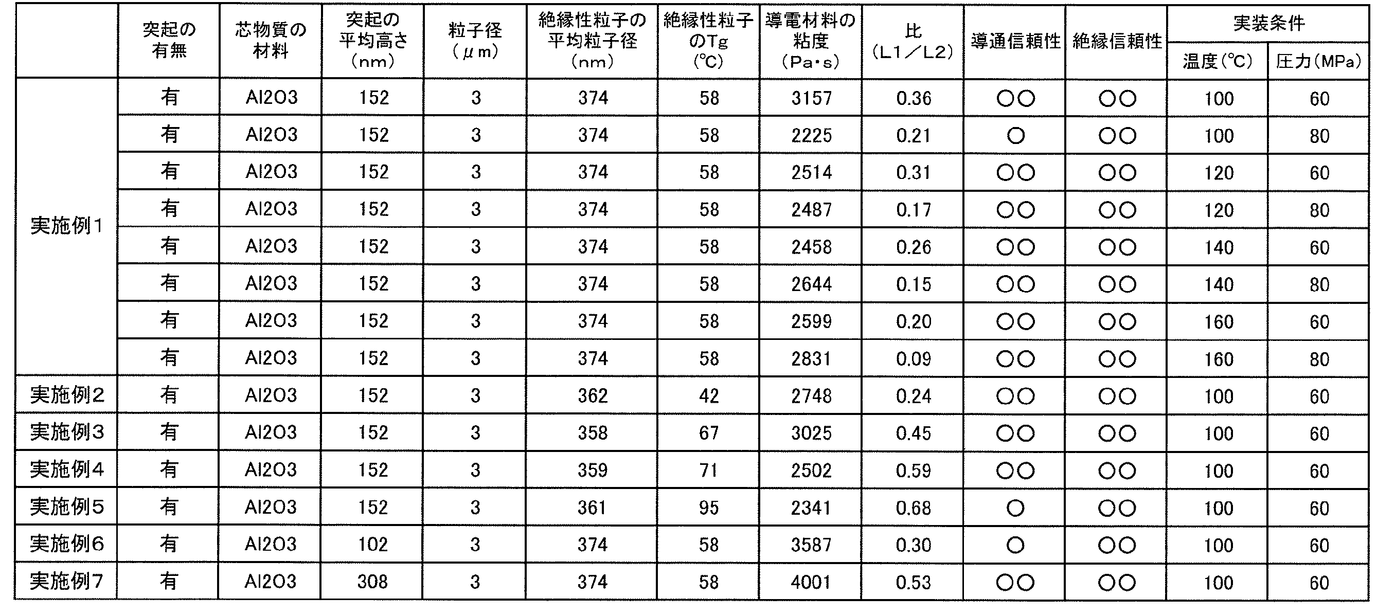
- Example 3 Except that tridecyl methacrylate used in the production of the insulating particles was changed to dodecyl methacrylate and that the average particle size of the insulating particles was set as shown in Table 1 below, the same as in Example 1. Then, conductive particles (conductive particles with insulating particles), anisotropic conductive paste, and connection structure were obtained.
- Example 5 Except that the tridecyl methacrylate used in the production of the insulating particles was changed to amyl methacrylate and that the average particle size of the insulating particles was set as shown in Table 1 below, the same as in Example 1. Then, conductive particles (conductive particles with insulating particles), anisotropic conductive paste, and connection structure were obtained.
- Example 6 Conductive particles (conductive particles with insulating particles), anisotropic conductive paste, and anisotropic conductive paste were used in the same manner as in Example 1 except that the average particle size of the alumina particle slurry used for preparing the conductive particles was changed to 102 nm. A connection structure was obtained.
- Example 9 Conductive particles (conductive particles with insulating particles), anisotropic conductive paste, and connection structure were obtained in the same manner as in Example 1 except that the average particle size of the insulating particles was changed to 156 nm.
- Example 10 Conductive particles (conductive particles with insulating particles), anisotropic conductive paste, and connection structure were obtained in the same manner as in Example 1 except that the average particle size of the insulating particles was changed to 511 nm.
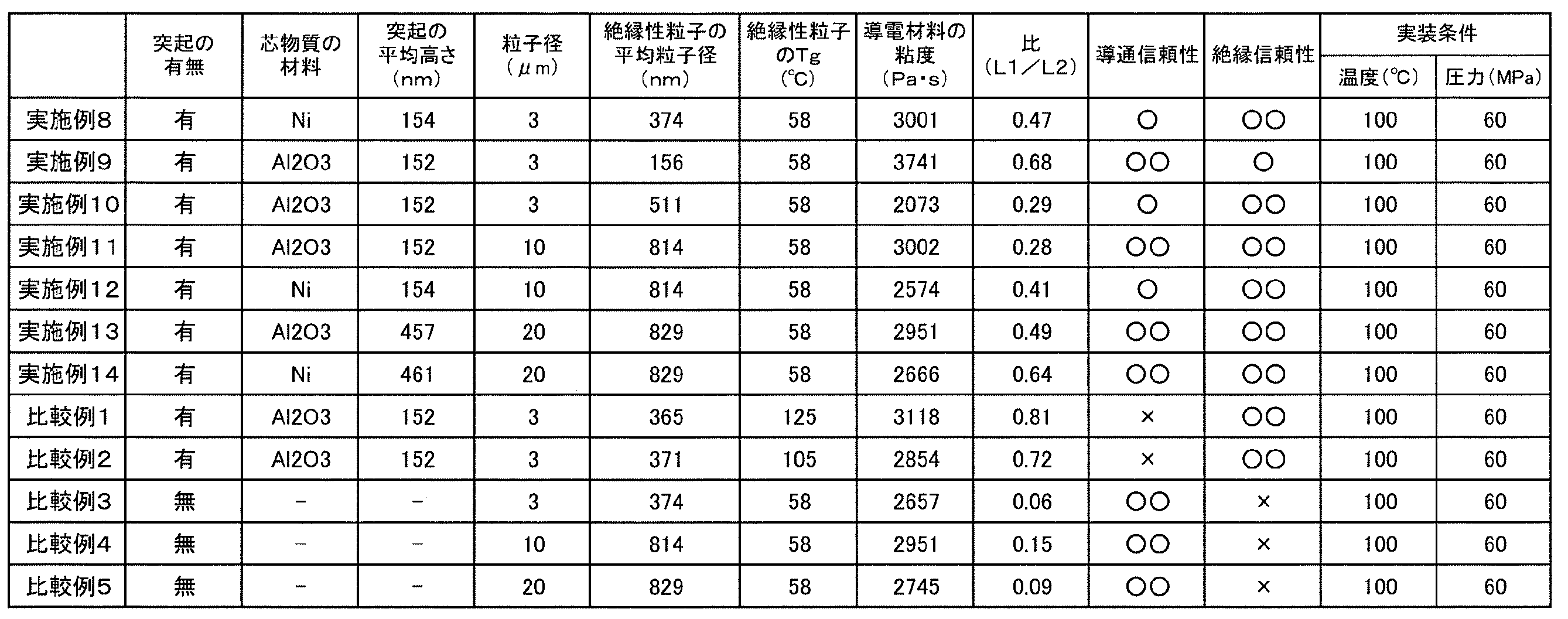
- Example 11 Conductive particles in the same manner as in Example 1 except that the average particle diameter of the base particle A was changed to 10 ⁇ m and the average particle diameter of the insulating particles was set as shown in Table 2 below. (Conductive particles with insulating particles), anisotropic conductive paste and connection structure were obtained.
- Example 14 The average particle size of the base particle A was changed to 20 ⁇ m, the alumina particle slurry used for producing the conductive particles was changed to the average particle size of the nickel particle slurry, 461 nm, and the average particle size of the insulating particles was changed to Except having set as shown in following Table 2, it carried out similarly to Example 1, and obtained electroconductive particle (electroconductive particle with an insulating particle), anisotropic conductive paste, and the connection structure.
- Example 1 The same as in Example 1 except that all the methacrylic acid esters used in the production of the insulating particles were changed to methyl methacrylate and the average particle size of the insulating particles was set as shown in Table 2 below. Thus, conductive particles (conductive particles with insulating particles), anisotropic conductive paste, and connection structure were obtained.
- Example 4 The average particle diameter of the base particle A was changed to 10 ⁇ m, the alumina particle slurry was not used when producing the conductive particles, and the average particle diameter of the insulating particles was set as shown in Table 2 below. Except that, conductive particles (conductive particles with insulating particles), an anisotropic conductive paste, and a connection structure were obtained in the same manner as Example 1.
- Viscosity of conductive material anisotropic conductive paste
- E-type viscometer (“TVE22L” manufactured by Toki Sangyo Co., Ltd.)
- the viscosity of the anisotropic conductive paste was measured under the conditions of 100 ° C. and 5 rpm. .
- ⁇ The ratio of the number of connection structures having a resistance value of 10 8 ⁇ or more is 80% or more.
- ⁇ The ratio of the number of connection structures having a resistance value of 10 8 ⁇ or more is 70% or more and less than 80%.
- the ratio of the number of connection structures having a value of 10 8 ⁇ or more is 60% or more and less than 70% ⁇ : The ratio of the number of connection structures having a resistance value of 10 8 ⁇ or more is less than 60%
Landscapes
- Engineering & Computer Science (AREA)
- Manufacturing & Machinery (AREA)
- Physics & Mathematics (AREA)
- Chemical & Material Sciences (AREA)
- Dispersion Chemistry (AREA)
- Spectroscopy & Molecular Physics (AREA)
- Thermal Sciences (AREA)
- Conductive Materials (AREA)
- Non-Insulated Conductors (AREA)
- Multi-Conductor Connections (AREA)
- Connections Effected By Soldering, Adhesion, Or Permanent Deformation (AREA)
Abstract
Description
本発明に係る導電性粒子は、導電性粒子本体と、絶縁部とを備える。上記導電性粒子本体は、導電部を有する。上記絶縁部は、上記導電性粒子本体の表面上に配置されている。本発明に係る導電性粒子では、上記導電性粒子本体が、上記導電部の外表面に複数の突起を有する。本発明に係る導電性粒子では、上記絶縁部のガラス転移温度が100℃未満である。本発明に係る導電性粒子では、上記絶縁部は、絶縁性粒子である。本発明に係る導電性粒子では、上記絶縁性粒子が、温度100℃~160℃及び圧力60MPa~80MPaの圧縮条件を満足する少なくとも1つの圧縮条件で圧縮されたときに、圧縮後の上記絶縁性粒子の圧縮方向での粒子径の最大値の、圧縮後の上記絶縁性粒子の圧縮方向と直交する方向での粒子径の最大値に対する比が0.7以下になるように変形可能である。本発明において、導電性粒子本体を、導電性粒子と呼ぶ場合に、絶縁部を備える導電性粒子を、絶縁部付き導電性粒子と呼ぶことができる。絶縁部が絶縁性粒子であるので、絶縁部付き導電性粒子は、絶縁性粒子付き導電性粒子である。
上記導電性粒子本体は、導電部の外表面に突起を有する。該突起は複数であることが好ましい。導電性粒子本体により接続される電極の表面には、酸化被膜が形成されていることが多い。導電部の外表面に突起を有する導電性粒子を用いることで、電極間に導電性粒子を配置して圧着させることにより、突起により上記酸化被膜を効果的に排除できる。このため、電極と導電部とがより一層確実に接触し、電極間の接続抵抗がより一層低くなる。さらに、電極間の接続時に、導電性粒子本体の突起によって、導電性粒子本体と電極との間の絶縁部を効果的に排除できる。また、本発明では、絶縁部のガラス転移温度が低いので、絶縁部を効果的に排除できる。
上記基材粒子としては、樹脂粒子、金属粒子を除く無機粒子、有機無機ハイブリッド粒子及び金属粒子等が挙げられる。上記基材粒子は、金属粒子を除く基材粒子であることが好ましく、樹脂粒子、金属粒子を除く無機粒子又は有機無機ハイブリッド粒子であることがより好ましい。上記基材粒子は、コアシェル粒子であってもよい。
上記導電部の材料である金属は特に限定されない。導電性粒子が、全体が導電部である金属粒子である場合、該金属粒子の材料である金属は特に限定されない。上記金属としては、例えば、金、銀、パラジウム、銅、白金、亜鉛、鉄、錫、鉛、アルミニウム、コバルト、インジウム、ニッケル、クロム、チタン、アンチモン、ビスマス、タリウム、ゲルマニウム、カドミウム、ケイ素及びこれらの合金等が挙げられる。また、上記金属としては、錫ドープ酸化インジウム(ITO)及びはんだ等が挙げられる。電極間の接続抵抗がより一層低くなるので、錫を含む合金、ニッケル、パラジウム、銅又は金が好ましく、ニッケル又はパラジウムが好ましい。
上記突起を形成する方法としては、基材粒子の表面に芯物質を付着させた後、無電解めっきにより導電部を形成する方法、並びに基材粒子の表面に無電解めっきにより導電部を形成した後、芯物質を付着させ、更に無電解めっきにより導電部を形成する方法等が挙げられる。上記突起を形成する他の方法としては、基材粒子の表面上に、第1の導電部を形成した後、該第1の導電部上に芯物質を配置し、次に第2の導電部を形成する方法、並びに基材粒子の表面上に導電部(第1の導電部又は第2の導電部等)を形成する途中段階で、芯物質を添加する方法等が挙げられる。また、突起を形成するために、上記芯物質を用いずに、基材粒子に無電解めっきにより導電部を形成した後、導電部の表面上に突起状にめっきを析出させ、更に無電解めっきにより導電部を形成する方法等を用いてもよい。
本発明に係る導電性粒子では、上記絶縁部は、絶縁性粒子である。上記絶縁部の材料としては、ポリオレフィン化合物、(メタ)アクリレート重合体、(メタ)アクリレート共重合体、ブロックポリマー、熱可塑性樹脂、熱可塑性樹脂の架橋物、熱硬化性樹脂及び水溶性樹脂等が挙げられる。上記絶縁部の材料は、1種のみが用いられてもよく、2種以上が併用されてもよい。
本発明に係る導電材料は、上述した導電性粒子と、バインダー樹脂とを含む。上記導電性粒子は、バインダー樹脂中に分散されて用いられることが好ましく、バインダー樹脂中に分散されて導電材料として用いられることが好ましい。上記導電材料は、異方性導電材料であることが好ましい。上記導電材料は、電極間の電気的な接続に用いられることが好ましい。上記導電材料は回路接続用導電材料であることが好ましい。
上記導電性粒子を用いて、又は上記導電性粒子とバインダー樹脂とを含む導電材料を用いて、接続対象部材を接続することにより、接続構造体を得ることができる。
(1)導電性粒子の作製
粒子径が3.0μmであるジビニルベンゼン共重合体樹脂粒子(基材粒子A、積水化学工業社製「ミクロパールSP-203」)を用意した。パラジウム触媒液を5重量%含むアルカリ溶液100重量部に、上記基材粒子A10重量部を、超音波分散器を用いて分散させた後、溶液をろ過することにより、基材粒子Aを取り出した。次いで、基材粒子Aをジメチルアミンボラン1重量%溶液100重量部に添加し、基材粒子Aの表面を活性化させた。表面が活性化された基材粒子Aを十分に水洗した後、蒸留水500重量部に加え、分散させることにより、分散液を得た。次に、アルミナ粒子スラリー(平均粒子径152nm)1gを3分間かけて上記分散液に添加し、芯物質が付着された基材粒子を含む懸濁液を得た。
4ツ口セパラブルカバー、攪拌翼、三方コック、冷却管及び温度プローブを取り付けた5000mLセパラブルフラスコに、蒸留水4000ml、エタノール900ml、メタクリル酸メチル3.3mol、メタクリル酸トリデシル4.1mol、アシッドホスホオキシポリオキシエチレングリコールメタクリレート0.5mmol、及び2,2’-アゾビス(2,4-ジメチルバレロニトリル)0.3mmolを含むモノマー組成物を入れた後、250rpmで攪拌し、窒素雰囲気下60℃で5時間重合を行った。反応終了後、凍結乾燥して、アシッドホスホオキシポリオキシエチレングリコールメタクリレートに由来するP-OH基を表面に有する絶縁性粒子(平均粒子径374nm)を得た。
上記で得られた絶縁性粒子をそれぞれ超音波照射下で蒸留水に分散させ、絶縁性粒子の10重量%水分散液を得た。得られた導電性粒子A10gを蒸留水500mLに分散させ、絶縁性粒子の10重量%水分散液1gを添加し、室温で8時間攪拌した。3μmのメッシュフィルターで濾過した後、更にメタノールで洗浄、乾燥し、導電性粒子(絶縁性粒子付き導電性粒子)を得た。
得られた導電性粒子(絶縁性粒子付き導電性粒子)7重量部と、ビスフェノールA型フェノキシ樹脂25重量部と、フルオレン型エポキシ樹脂4重量部と、フェノールノボラック型エポキシ樹脂30重量部と、SI-60L(三新化学工業社製)とを配合して、3分間脱泡及び攪拌することで、異方性導電ペーストを得た。
L/Sが10μm/20μmであるIZO電極パターン(第1の電極、電極表面の金属のビッカース硬度100Hv)が上面に形成された透明ガラス基板を用意した。また、L/Sが10μm/20μmであるAu電極パターン(第2の電極、電極表面の金属のビッカース硬度50Hv)が下面に形成された半導体チップを用意した。
絶縁性粒子の作製時に使用するメタクリル酸トリデシルをメタクリル酸ステアリルに変更したこと、並びに、絶縁性粒子の平均粒子径を下記の表1に示すように設定したこと以外は実施例1と同様にして、導電性粒子(絶縁性粒子付き導電性粒子)、異方性導電ペースト及び接続構造体を得た。
絶縁性粒子の作製時に使用するメタクリル酸トリデシルをメタクリル酸ドデシルに変更したこと、並びに、絶縁性粒子の平均粒子径を下記の表1に示すように設定したこと以外は実施例1と同様にして、導電性粒子(絶縁性粒子付き導電性粒子)、異方性導電ペースト及び接続構造体を得た。
絶縁性粒子の作製時に使用するメタクリル酸トリデシルをメタクリル酸オクチルに変更したこと、並びに、絶縁性粒子の平均粒子径を下記の表1に示すように設定したこと以外は実施例1と同様にして、導電性粒子(絶縁性粒子付き導電性粒子)、異方性導電ペースト及び接続構造体を得た。
絶縁性粒子の作製時に使用するメタクリル酸トリデシルをメタクリル酸アミルに変更したこと、並びに、絶縁性粒子の平均粒子径を下記の表1に示すように設定したこと以外は実施例1と同様にして、導電性粒子(絶縁性粒子付き導電性粒子)、異方性導電ペースト及び接続構造体を得た。
導電性粒子の作製時に使用するアルミナ粒子スラリーの平均粒子径を102nmに変更したこと以外は実施例1と同様にして、導電性粒子(絶縁性粒子付き導電性粒子)、異方性導電ペースト及び接続構造体を得た。
導電性粒子の作製時に使用するアルミナ粒子スラリーの平均粒子径を308nmに変更したこと以外は実施例1と同様にして、導電性粒子(絶縁性粒子付き導電性粒子)、異方性導電ペースト及び接続構造体を得た。
導電性粒子の作製時に使用するアルミナ粒子スラリーをニッケル粒子スラリー(平均粒子径154nm)に変更したこと以外は実施例1と同様にして、導電性粒子(絶縁性粒子付き導電性粒子)、異方性導電ペースト及び接続構造体を得た。
絶縁性粒子の平均粒子径を156nmに変更したこと以外は実施例1と同様にして、導電性粒子(絶縁性粒子付き導電性粒子)、異方性導電ペースト及び接続構造体を得た。
絶縁性粒子の平均粒子径を511nmに変更したこと以外は実施例1と同様にして、導電性粒子(絶縁性粒子付き導電性粒子)、異方性導電ペースト及び接続構造体を得た。
基材粒子Aの平均粒子径を10μmに変更したこと、並びに、絶縁性粒子の平均粒子径を下記の表2に示すように設定したこと以外は、実施例1と同様にして、導電性粒子(絶縁性粒子付き導電性粒子)、異方性導電ペースト及び接続構造体を得た。
基材粒子Aの平均粒子径を10μmに変更したこと、導電性粒子の作製時に使用するアルミナ粒子スラリーをニッケル粒子スラリー(平均粒子径154nm)に変更したこと、並びに、絶縁性粒子の平均粒子径を下記の表2に示すように設定したこと以外は、実施例1と同様にして、導電性粒子(絶縁性粒子付き導電性粒子)、異方性導電ペースト及び接続構造体を得た。
基材粒子Aの平均粒子径を20μmに変更したこと、導電性粒子の作製時に使用するアルミナ粒子スラリーの平均粒子径を457nmに変更したこと、並びに、絶縁性粒子の平均粒子径を下記の表2に示すように設定したこと以外は、実施例1と同様にして、導電性粒子(絶縁性粒子付き導電性粒子)、異方性導電ペースト及び接続構造体を得た。
基材粒子Aの平均粒子径を20μmに変更したこと、導電性粒子の作製時に使用するアルミナ粒子スラリーをニッケル粒子スラリーの平均粒子径461nmに変更したこと、並びに、絶縁性粒子の平均粒子径を下記の表2に示すように設定したこと以外は、実施例1と同様にして、導電性粒子(絶縁性粒子付き導電性粒子)、異方性導電ペースト及び接続構造体を得た。
絶縁性粒子の作製時に使用するメタクリル酸エステルを全てメタクリル酸メチルに変更したこと、並びに、絶縁性粒子の平均粒子径を下記の表2に示すように設定したこと以外は実施例1と同様にして、導電性粒子(絶縁性粒子付き導電性粒子)、異方性導電ペースト及び接続構造体を得た。
絶縁性粒子の作製時に使用するメタクリル酸トリデシルをメタクリル酸ブチルに変更したこと、並びに、絶縁性粒子の平均粒子径を下記の表2に示すように設定したこと以外は実施例1と同様にして、導電性粒子(絶縁性粒子付き導電性粒子)、異方性導電ペースト及び接続構造体を得た。
導電性粒子の作製時にアルミナ粒子スラリーを使用しなかったこと以外は実施例1と同様にして、導電性粒子(絶縁性粒子付き導電性粒子)、異方性導電ペースト及び接続構造体を得た。
基材粒子Aの平均粒子径を10μmに変更したこと、導電性粒子の作製時にアルミナ粒子スラリーを使用しなかったこと、並びに、絶縁性粒子の平均粒子径を下記の表2に示すように設定したこと以外は実施例1と同様にして、導電性粒子(絶縁性粒子付き導電性粒子)、異方性導電ペースト及び接続構造体を得た。
基材粒子Aの平均粒子径を20μmに変更したこと、導電性粒子の作製時にアルミナ粒子スラリーを使用しなかったこと、並びに、絶縁性粒子の平均粒子径を下記の表2に示すように設定したこと以外は実施例1と同様にして、導電性粒子(絶縁性粒子付き導電性粒子)、異方性導電ペースト及び接続構造体を得た。
(1)導電材料(異方性導電ペースト)の粘度
E型粘度計(東機産業社製「TVE22L」)を用いて、異方性導電ペーストの粘度を、100℃及び5rpmの条件で測定した。
FIB-SEM複合装置を用いて、得られた接続構造体の薄膜切片のSEM画像を観察した。得られた接続構造体において、導電性粒子と透明ガラス基板の間に挟まれた絶縁性粒子10個の変形量(上述した比L1/L2)を測定し、測定値の平均値を求めた。
実施例1と同様の方法で作製された20個の接続構造体の上下の電極間の接続抵抗をそれぞれ、4端子法により測定した。なお、電圧=電流×抵抗の関係から、一定の電流を流した時の電圧を測定することにより接続抵抗を求めることができる。導通信頼性を下記の基準で判定した。
○○:接続抵抗が2.0Ω以下
○:接続抵抗が2.0Ωを超え、3.0Ω以下
△:接続抵抗が3.0Ωを超え、5.0Ω以下
×:接続抵抗が5.0Ωを超える
上記(3)導通信頼性の評価で得られた20個の接続構造体において、隣接する電極間のリークの有無を、テスターで抵抗を測定することにより評価した。絶縁性を下記の基準で判定した。
○○:抵抗値が108Ω以上の接続構造体の個数の割合が80%以上
○:抵抗値が108Ω以上の接続構造体の個数の割合が70%以上、80%未満
△:抵抗値が108Ω以上の接続構造体の個数の割合が60%以上、70%未満
×:抵抗値が108Ω以上の接続構造体の個数の割合が60%未満
2,2A,2B…導電性粒子本体
3…絶縁性粒子
3C…絶縁層
11…基材粒子
12,12A,12B…導電部
12AA…第1の導電部
12AB…第2の導電部
13…芯物質
51…接続構造体
52…第1の接続対象部材
52a…第1の電極
53…第2の接続対象部材
53a…第2の電極
54…接続部
Claims (12)
- 導電部を有する導電性粒子本体と、前記導電性粒子本体の表面上に配置された絶縁性粒子とを備え、
前記導電性粒子本体が、前記導電部の外表面に複数の突起を有し、
前記絶縁性粒子のガラス転移温度が100℃未満であり、
前記絶縁性粒子が、温度100℃~160℃及び圧力60MPa~80MPaの圧縮条件を満足する少なくとも1つの圧縮条件で圧縮されたときに、圧縮後の前記絶縁性粒子の圧縮方向での粒子径の最大値の、圧縮後の前記絶縁性粒子の圧縮方向と直交する方向での粒子径の最大値に対する比が0.7以下になるように変形可能である、導電性粒子。 - 前記導電性粒子本体の表面上に複数の前記絶縁性粒子が配置されている、請求項1に記載の導電性粒子。
- 前記絶縁性粒子の平均粒子径の前記突起の平均高さに対する比が0.5を超える、請求項2に記載の導電性粒子。
- 前記絶縁性粒子が、温度100℃及び圧力60MPaで圧縮されたときに、圧縮後の前記絶縁性粒子の圧縮方向での粒子径の最大値の、圧縮後の前記絶縁性粒子の圧縮方向と直交する方向での粒子径の最大値に対する比が0.7以下になるように変形可能である、請求項1~3のいずれか1項に記載の導電性粒子。
- 前記絶縁性粒子が、温度100℃~160℃及び圧力60MPa~80MPaの圧縮条件を満足する少なくとも1つの圧縮条件で圧縮されたときに、圧縮後の前記絶縁性粒子の圧縮方向での粒子径の最大値が、圧縮前の前記突起の平均高さ以下になるように変形可能である、請求項1~4のいずれか1項に記載の導電性粒子。
- 前記絶縁性粒子が、温度100℃及び圧力60MPa圧縮されたときに、圧縮後の前記絶縁性粒子の圧縮方向での粒子径の最大値が、圧縮前の前記突起の平均高さ以下になるように変形可能である、請求項5に記載の導電性粒子。
- 120℃以下で熱圧着することにより、導電接続するために用いられる、請求項1~6のいずれか1項に記載の導電性粒子。
- 請求項1~7のいずれか1項に記載の導電性粒子と、バインダー樹脂とを含む、導電材料。
- 導電材料の100℃での粘度が1000Pa・s以上、5000Pa・s以下である、請求項8に記載の導電材料。
- 第1の電極を表面に有する第1の接続対象部材と、
第2の電極を表面に有する第2の接続対象部材と、
前記第1の接続対象部材と、前記第2の接続対象部材を接続している接続部とを備え、
前記接続部の材料が、請求項1~7のいずれか1項に記載の導電性粒子であるか、又は前記導電性粒子とバインダー樹脂とを含む導電材料であり、
前記第1の電極と前記第2の電極とが、前記導電性粒子における前記導電性粒子本体により電気的に接続されている、接続構造体。 - 第1の電極を表面に有する第1の接続対象部材と、第2の電極を表面に有する第2の接続対象部材との間に、請求項1~7のいずれか1項に記載の導電性粒子を配置するか、又は前記導電性粒子とバインダー樹脂とを含む導電材料を配置する工程と、
前記絶縁性粒子のガラス転移温度以上、160℃以下で熱圧着することにより、導電接続する工程とを備える、接続構造体の製造方法。 - 前記絶縁性粒子のガラス転移温度以上、120℃以下で熱圧着する、請求項11に記載の接続構造体の製造方法。
Priority Applications (4)
| Application Number | Priority Date | Filing Date | Title |
|---|---|---|---|
| JP2017531411A JP7028641B2 (ja) | 2016-05-19 | 2017-05-17 | 導電材料及び接続構造体 |
| KR1020187014628A KR102398998B1 (ko) | 2016-05-19 | 2017-05-17 | 도전성 입자, 도전 재료 및 접속 구조체 |
| CN201780017468.3A CN108780677B (zh) | 2016-05-19 | 2017-05-17 | 导电性粒子、导电材料以及连接结构体 |
| JP2021192833A JP7381547B2 (ja) | 2016-05-19 | 2021-11-29 | 導電性粒子、導電材料及び接続構造体 |
Applications Claiming Priority (2)
| Application Number | Priority Date | Filing Date | Title |
|---|---|---|---|
| JP2016-100595 | 2016-05-19 | ||
| JP2016100595 | 2016-05-19 |
Publications (1)
| Publication Number | Publication Date |
|---|---|
| WO2017199987A1 true WO2017199987A1 (ja) | 2017-11-23 |
Family
ID=60325240
Family Applications (1)
| Application Number | Title | Priority Date | Filing Date |
|---|---|---|---|
| PCT/JP2017/018462 Ceased WO2017199987A1 (ja) | 2016-05-19 | 2017-05-17 | 導電性粒子、導電材料及び接続構造体 |
Country Status (5)
| Country | Link |
|---|---|
| JP (2) | JP7028641B2 (ja) |
| KR (1) | KR102398998B1 (ja) |
| CN (1) | CN108780677B (ja) |
| TW (1) | TWI774675B (ja) |
| WO (1) | WO2017199987A1 (ja) |
Cited By (1)
| Publication number | Priority date | Publication date | Assignee | Title |
|---|---|---|---|---|
| CN111902884A (zh) * | 2018-04-04 | 2020-11-06 | 积水化学工业株式会社 | 带有绝缘性粒子的导电性粒子、带有绝缘性粒子的导电性粒子的制造方法、导电材料以及连接结构体 |
Families Citing this family (2)
| Publication number | Priority date | Publication date | Assignee | Title |
|---|---|---|---|---|
| WO2022044913A1 (ja) * | 2020-08-24 | 2022-03-03 | 日本化学工業株式会社 | 被覆粒子及びその製造方法 |
| JP7791737B2 (ja) | 2022-02-16 | 2025-12-24 | オリエンタルモーター株式会社 | 発電センサ |
Citations (5)
| Publication number | Priority date | Publication date | Assignee | Title |
|---|---|---|---|---|
| JP2005044773A (ja) * | 2003-07-07 | 2005-02-17 | Sekisui Chem Co Ltd | 被覆導電性粒子、異方性導電材料及び導電接続構造体 |
| JP2007537572A (ja) * | 2004-05-12 | 2007-12-20 | マイクログローブ コープ カンパニー リミテッド | 異方性導電接続用の絶縁導電性粒子及びその製造方法並びにこれを用いた異方性導電接続材料 |
| JP2012124035A (ja) * | 2010-12-08 | 2012-06-28 | Nippon Shokubai Co Ltd | 樹脂粒子およびこれを用いた絶縁化導電性粒子並びに異方性導電材料 |
| JP2014017213A (ja) * | 2012-07-11 | 2014-01-30 | Hitachi Chemical Co Ltd | 絶縁被覆導電粒子及びそれを用いた異方導電性接着剤 |
| JP2015187984A (ja) * | 2014-03-10 | 2015-10-29 | 積水化学工業株式会社 | 絶縁性粒子付き導電性粒子、導電材料及び接続構造体 |
Family Cites Families (10)
| Publication number | Priority date | Publication date | Assignee | Title |
|---|---|---|---|---|
| JPH05334912A (ja) * | 1992-06-01 | 1993-12-17 | Casio Comput Co Ltd | 異方性導電接着剤および導電接続構造 |
| JP3904798B2 (ja) * | 1999-04-01 | 2007-04-11 | 三井化学株式会社 | 異方導電性ペースト |
| CN100437838C (zh) * | 2003-07-07 | 2008-11-26 | 积水化学工业株式会社 | 包覆导电性粒子、各向异性导电材料以及导电连接结构体 |
| KR101271814B1 (ko) * | 2009-07-02 | 2013-06-07 | 히타치가세이가부시끼가이샤 | 도전 입자 |
| JP5498907B2 (ja) | 2010-09-29 | 2014-05-21 | 株式会社日本触媒 | 樹脂粒子およびこれを用いた絶縁化導電性粒子並びに異方性導電材料 |
| WO2012137335A1 (ja) * | 2011-04-07 | 2012-10-11 | 日立化成工業株式会社 | 回路接続材料及びその使用並びに接続構造体及びその製造方法 |
| KR101962977B1 (ko) * | 2011-07-28 | 2019-03-27 | 세키스이가가쿠 고교가부시키가이샤 | 도전성 입자, 도전 재료 및 접속 구조체 |
| JP2013214417A (ja) * | 2012-04-02 | 2013-10-17 | Hitachi Chemical Co Ltd | 回路接続材料、回路部材接続構造体及び回路部材接続構造体の製造方法 |
| KR20150092077A (ko) * | 2012-12-06 | 2015-08-12 | 세키스이가가쿠 고교가부시키가이샤 | 도전 재료, 접속 구조체 및 접속 구조체의 제조 방법 |
| JP6114557B2 (ja) * | 2013-01-10 | 2017-04-12 | 積水化学工業株式会社 | 導電材料及び接続構造体の製造方法 |
-
2017
- 2017-05-17 JP JP2017531411A patent/JP7028641B2/ja active Active
- 2017-05-17 WO PCT/JP2017/018462 patent/WO2017199987A1/ja not_active Ceased
- 2017-05-17 CN CN201780017468.3A patent/CN108780677B/zh active Active
- 2017-05-17 KR KR1020187014628A patent/KR102398998B1/ko active Active
- 2017-05-18 TW TW106116423A patent/TWI774675B/zh active
-
2021
- 2021-11-29 JP JP2021192833A patent/JP7381547B2/ja active Active
Patent Citations (5)
| Publication number | Priority date | Publication date | Assignee | Title |
|---|---|---|---|---|
| JP2005044773A (ja) * | 2003-07-07 | 2005-02-17 | Sekisui Chem Co Ltd | 被覆導電性粒子、異方性導電材料及び導電接続構造体 |
| JP2007537572A (ja) * | 2004-05-12 | 2007-12-20 | マイクログローブ コープ カンパニー リミテッド | 異方性導電接続用の絶縁導電性粒子及びその製造方法並びにこれを用いた異方性導電接続材料 |
| JP2012124035A (ja) * | 2010-12-08 | 2012-06-28 | Nippon Shokubai Co Ltd | 樹脂粒子およびこれを用いた絶縁化導電性粒子並びに異方性導電材料 |
| JP2014017213A (ja) * | 2012-07-11 | 2014-01-30 | Hitachi Chemical Co Ltd | 絶縁被覆導電粒子及びそれを用いた異方導電性接着剤 |
| JP2015187984A (ja) * | 2014-03-10 | 2015-10-29 | 積水化学工業株式会社 | 絶縁性粒子付き導電性粒子、導電材料及び接続構造体 |
Cited By (2)
| Publication number | Priority date | Publication date | Assignee | Title |
|---|---|---|---|---|
| CN111902884A (zh) * | 2018-04-04 | 2020-11-06 | 积水化学工业株式会社 | 带有绝缘性粒子的导电性粒子、带有绝缘性粒子的导电性粒子的制造方法、导电材料以及连接结构体 |
| CN111902884B (zh) * | 2018-04-04 | 2023-03-14 | 积水化学工业株式会社 | 导电性粒子、其制造方法、导电材料及连接结构体 |
Also Published As
| Publication number | Publication date |
|---|---|
| JP7028641B2 (ja) | 2022-03-02 |
| KR20190008828A (ko) | 2019-01-25 |
| KR102398998B1 (ko) | 2022-05-17 |
| TWI774675B (zh) | 2022-08-21 |
| JP7381547B2 (ja) | 2023-11-15 |
| JPWO2017199987A1 (ja) | 2019-03-14 |
| TW201812790A (zh) | 2018-04-01 |
| CN108780677B (zh) | 2020-12-08 |
| JP2022022293A (ja) | 2022-02-03 |
| CN108780677A (zh) | 2018-11-09 |
Similar Documents
| Publication | Publication Date | Title |
|---|---|---|
| JP6034177B2 (ja) | 導電性粒子、導電材料及び接続構造体 | |
| WO2014007237A1 (ja) | 絶縁性粒子付き導電性粒子、導電材料及び接続構造体 | |
| WO2018181694A1 (ja) | 導電性粒子、導電材料及び接続構造体 | |
| WO2013108740A1 (ja) | 導電性粒子、導電材料及び接続構造体 | |
| JP7381547B2 (ja) | 導電性粒子、導電材料及び接続構造体 | |
| WO2015037711A1 (ja) | 導電性粒子、導電材料及び接続構造体 | |
| CN111954909A (zh) | 带有绝缘性粒子的导电性粒子、导电材料以及连接结构体 | |
| JP2017069191A (ja) | 導電性粒子、導電材料及び接続構造体 | |
| WO2016063941A1 (ja) | 導電性粒子、導電材料及び接続構造体 | |
| CN103782351A (zh) | 导电性粒子、导电材料及连接结构体 | |
| JP7180981B2 (ja) | 導電性粒子、導電材料及び接続構造体 | |
| WO2017051872A1 (ja) | 接続構造体の製造方法、導電性粒子、導電フィルム及び接続構造体 | |
| JP2016154139A (ja) | 導電性粒子粉体、導電性粒子粉体の製造方法、導電材料及び接続構造体 | |
| JP6457743B2 (ja) | 接続構造体 | |
| JP6646366B2 (ja) | 導電性粒子、導電材料及び接続構造体 | |
| CN110603612B (zh) | 导电性粒子、导电性粒子的制造方法、导电材料以及连接结构体 | |
| JP6568467B2 (ja) | 導電性粒子、導電材料及び接続構造体 | |
| JP6345075B2 (ja) | 導電性粒子、導電材料及び接続構造体 | |
| KR102793665B1 (ko) | 절연성 입자 구비 도전성 입자, 도전 재료 및 접속 구조체 | |
| JP6333624B2 (ja) | 接続構造体 | |
| JP2015056306A (ja) | 導電性粒子、導電材料及び接続構造体 | |
| WO2019194134A1 (ja) | 絶縁性粒子付き導電性粒子、絶縁性粒子付き導電性粒子の製造方法、導電材料及び接続構造体 | |
| WO2019194133A1 (ja) | 絶縁性粒子付き導電性粒子、絶縁性粒子付き導電性粒子の製造方法、導電材料及び接続構造体 | |
| JP2020013787A (ja) | 導電材料及び接続構造体 | |
| JP2015057769A (ja) | 導電性粒子、導電材料及び接続構造体 |
Legal Events
| Date | Code | Title | Description |
|---|---|---|---|
| ENP | Entry into the national phase |
Ref document number: 2017531411 Country of ref document: JP Kind code of ref document: A |
|
| ENP | Entry into the national phase |
Ref document number: 20187014628 Country of ref document: KR Kind code of ref document: A |
|
| NENP | Non-entry into the national phase |
Ref country code: DE |
|
| 121 | Ep: the epo has been informed by wipo that ep was designated in this application |
Ref document number: 17799411 Country of ref document: EP Kind code of ref document: A1 |
|
| 122 | Ep: pct application non-entry in european phase |
Ref document number: 17799411 Country of ref document: EP Kind code of ref document: A1 |