WO2017199609A1 - Élément de revêtement et filtre de transfert - Google Patents
Élément de revêtement et filtre de transfert Download PDFInfo
- Publication number
- WO2017199609A1 WO2017199609A1 PCT/JP2017/014054 JP2017014054W WO2017199609A1 WO 2017199609 A1 WO2017199609 A1 WO 2017199609A1 JP 2017014054 W JP2017014054 W JP 2017014054W WO 2017199609 A1 WO2017199609 A1 WO 2017199609A1
- Authority
- WO
- WIPO (PCT)
- Prior art keywords
- region
- layer
- antireflection
- hard coat
- cover component
- Prior art date
Links
- 238000004040 coloring Methods 0.000 claims description 7
- 239000001052 yellow pigment Substances 0.000 claims description 4
- 239000006096 absorbing agent Substances 0.000 claims description 3
- 230000001788 irregular Effects 0.000 abstract 1
- 239000010410 layer Substances 0.000 description 80
- 238000004519 manufacturing process Methods 0.000 description 24
- 230000005540 biological transmission Effects 0.000 description 15
- 230000004313 glare Effects 0.000 description 13
- 239000011347 resin Substances 0.000 description 12
- 229920005989 resin Polymers 0.000 description 12
- 239000000463 material Substances 0.000 description 9
- 239000012790 adhesive layer Substances 0.000 description 8
- 230000006870 function Effects 0.000 description 7
- 239000000758 substrate Substances 0.000 description 7
- 239000011324 bead Substances 0.000 description 6
- 239000011521 glass Substances 0.000 description 6
- 238000000034 method Methods 0.000 description 6
- 238000000465 moulding Methods 0.000 description 5
- 230000015572 biosynthetic process Effects 0.000 description 4
- 230000006866 deterioration Effects 0.000 description 4
- 239000002245 particle Substances 0.000 description 4
- 229920000139 polyethylene terephthalate Polymers 0.000 description 4
- 239000005020 polyethylene terephthalate Substances 0.000 description 4
- 230000032683 aging Effects 0.000 description 3
- 230000003373 anti-fouling effect Effects 0.000 description 3
- 238000009792 diffusion process Methods 0.000 description 3
- 230000009993 protective function Effects 0.000 description 3
- 238000005034 decoration Methods 0.000 description 2
- 230000000694 effects Effects 0.000 description 2
- 238000005755 formation reaction Methods 0.000 description 2
- 238000007646 gravure printing Methods 0.000 description 2
- 238000005286 illumination Methods 0.000 description 2
- 238000007641 inkjet printing Methods 0.000 description 2
- 239000004973 liquid crystal related substance Substances 0.000 description 2
- 230000007935 neutral effect Effects 0.000 description 2
- 229920003229 poly(methyl methacrylate) Polymers 0.000 description 2
- -1 polyethylene terephthalate Polymers 0.000 description 2
- 239000004926 polymethyl methacrylate Substances 0.000 description 2
- 238000007650 screen-printing Methods 0.000 description 2
- 239000004793 Polystyrene Substances 0.000 description 1
- 238000010521 absorption reaction Methods 0.000 description 1
- 229920000122 acrylonitrile butadiene styrene Polymers 0.000 description 1
- 239000003086 colorant Substances 0.000 description 1
- 230000007423 decrease Effects 0.000 description 1
- 238000010586 diagram Methods 0.000 description 1
- 238000005323 electroforming Methods 0.000 description 1
- 238000005530 etching Methods 0.000 description 1
- 238000001746 injection moulding Methods 0.000 description 1
- 238000010030 laminating Methods 0.000 description 1
- 230000031700 light absorption Effects 0.000 description 1
- 230000003287 optical effect Effects 0.000 description 1
- 239000000049 pigment Substances 0.000 description 1
- 238000007747 plating Methods 0.000 description 1
- 239000004417 polycarbonate Substances 0.000 description 1
- 229920000515 polycarbonate Polymers 0.000 description 1
- 229920005672 polyolefin resin Polymers 0.000 description 1
- 238000007639 printing Methods 0.000 description 1
- 239000004576 sand Substances 0.000 description 1
- 238000005488 sandblasting Methods 0.000 description 1
- 239000013589 supplement Substances 0.000 description 1
- 230000003746 surface roughness Effects 0.000 description 1
Images


Classifications
-
- G—PHYSICS
- G02—OPTICS
- G02B—OPTICAL ELEMENTS, SYSTEMS OR APPARATUS
- G02B1/00—Optical elements characterised by the material of which they are made; Optical coatings for optical elements
- G02B1/10—Optical coatings produced by application to, or surface treatment of, optical elements
- G02B1/11—Anti-reflection coatings
- G02B1/118—Anti-reflection coatings having sub-optical wavelength surface structures designed to provide an enhanced transmittance, e.g. moth-eye structures
-
- G—PHYSICS
- G02—OPTICS
- G02B—OPTICAL ELEMENTS, SYSTEMS OR APPARATUS
- G02B1/00—Optical elements characterised by the material of which they are made; Optical coatings for optical elements
- G02B1/10—Optical coatings produced by application to, or surface treatment of, optical elements
-
- G—PHYSICS
- G02—OPTICS
- G02B—OPTICAL ELEMENTS, SYSTEMS OR APPARATUS
- G02B1/00—Optical elements characterised by the material of which they are made; Optical coatings for optical elements
- G02B1/10—Optical coatings produced by application to, or surface treatment of, optical elements
- G02B1/14—Protective coatings, e.g. hard coatings
-
- G—PHYSICS
- G02—OPTICS
- G02B—OPTICAL ELEMENTS, SYSTEMS OR APPARATUS
- G02B5/00—Optical elements other than lenses
- G02B5/02—Diffusing elements; Afocal elements
-
- G—PHYSICS
- G02—OPTICS
- G02B—OPTICAL ELEMENTS, SYSTEMS OR APPARATUS
- G02B5/00—Optical elements other than lenses
- G02B5/20—Filters
- G02B5/208—Filters for use with infrared or ultraviolet radiation, e.g. for separating visible light from infrared and/or ultraviolet radiation
-
- G—PHYSICS
- G02—OPTICS
- G02B—OPTICAL ELEMENTS, SYSTEMS OR APPARATUS
- G02B5/00—Optical elements other than lenses
- G02B5/20—Filters
- G02B5/22—Absorbing filters
-
- G—PHYSICS
- G09—EDUCATION; CRYPTOGRAPHY; DISPLAY; ADVERTISING; SEALS
- G09F—DISPLAYING; ADVERTISING; SIGNS; LABELS OR NAME-PLATES; SEALS
- G09F9/00—Indicating arrangements for variable information in which the information is built-up on a support by selection or combination of individual elements
-
- H—ELECTRICITY
- H05—ELECTRIC TECHNIQUES NOT OTHERWISE PROVIDED FOR
- H05B—ELECTRIC HEATING; ELECTRIC LIGHT SOURCES NOT OTHERWISE PROVIDED FOR; CIRCUIT ARRANGEMENTS FOR ELECTRIC LIGHT SOURCES, IN GENERAL
- H05B33/00—Electroluminescent light sources
- H05B33/02—Details
-
- H—ELECTRICITY
- H10—SEMICONDUCTOR DEVICES; ELECTRIC SOLID-STATE DEVICES NOT OTHERWISE PROVIDED FOR
- H10K—ORGANIC ELECTRIC SOLID-STATE DEVICES
- H10K50/00—Organic light-emitting devices
Definitions
- the present disclosure relates to a cover component that covers the surface of a display panel such as an in-vehicle display device or a mobile device, and a transfer film used for manufacturing the cover component.
- Such a cover component has a structure in which, for example, a hard coat layer having a protective function and an antifouling function for a display panel and a decorative layer having a decorative function are provided on a transparent substrate.
- the decorative layer is composed of a frame-shaped colored layer and a transmission region provided inside the colored region.
- the transmissive area is a space for displaying the contents of the display panel, and the colored area is an area for giving a design to the edge of the display panel.
- the light generated from the inside of the display panel for example, the light generated from the backlight of the liquid crystal panel or the organic EL panel itself may pass through the transmission region and cause glare to the viewer. Further, light outside the display panel, such as sunlight or illumination light, may be reflected on the surface of the cover component to give glare (also referred to as glare) to the viewer.
- glare also referred to as glare
- the hard coat layer it is conceivable that a fine uneven shape is provided on the surface of the region overlapping the transmission region of the decorative layer.
- a fine irregularity By providing fine irregularities on the surface of the hard coat layer, the light from the inside of the display panel side and the light from the outside of the display panel can be diffused by the hard coat layer. It becomes possible to suppress the dazzling given.
- the cover component according to the present disclosure is a cover component that covers the surface of a display panel, and includes a decorative layer composed of a frame-shaped colored region and a transmissive region provided inside the colored region, and at least one side An antireflection layer including an antireflection region in which a fine uneven shape is formed, and the antireflection layer overlaps the decorative layer, the antireflection region covers the transmission region, and It protrudes to the colored region over the entire inner periphery of the colored region.
- the cover component according to the present disclosure is formed so that the antireflection region having a fine unevenness formed on at least one surface covers the transmission region and protrudes into the coloring region over the entire inner periphery of the coloring region. For this reason, even if a misalignment occurs between the antireflection area and the transmission area, the antireflection area overlaps the transmission area, so that the above-described light leakage and glare can be suppressed, and as a result, the quality of the cover parts decreases. Can be suppressed.
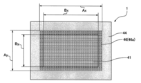
- FIG. 1A is an exploded perspective view of a cover part according to Embodiment 1.
- FIG. 1B is a plan view of the cover part according to Embodiment 1.
- FIG. 1C is a side cross-sectional view of the cover component according to Embodiment 1.
- FIG. 2 is an enlarged cross-sectional view illustrating a preferable aspect of the fine uneven shape of the cover component according to the first embodiment.
- 3A is a plan view of a transfer film used for manufacturing the cover component according to Embodiment 1.
- FIG. 3B is a side cross-sectional view of the transfer film according to Embodiment 1.
- FIG. 4A is a side cross-sectional view of the cover part manufacturing apparatus according to Embodiment 1.
- FIG. 4B is a side cross-sectional view of the manufacturing apparatus according to Embodiment 1.
- FIG. FIG. 5 is an enlarged cross-sectional view illustrating a preferable aspect of the fine uneven shape of the manufacturing apparatus according to the first embodiment.
- 6A is a plan view of a cover component according to Embodiment 2.
- FIG. 6B is a side cross-sectional view of the cover component according to Embodiment 2.
- FIG. 7 is a schematic cross-sectional view of a fine concavo-convex shape of the cover component manufacturing apparatus according to the second embodiment.
- FIG. 8A is an enlarged cross-sectional view illustrating a preferable aspect of the fine uneven shape of the manufacturing apparatus according to Embodiment 2.
- FIG. 8B is an enlarged cross-sectional view showing a preferable aspect of the fine uneven shape of the manufacturing apparatus according to Embodiment 2.
- FIG. 9A is a plan view of a cover part according to Embodiment 3.
- FIG. 9B is a side cross-sectional view of the cover part according to Embodiment 3.
- FIG. 10A is a plan view of a transfer film used for manufacturing a cover part according to Embodiment 3.
- FIG. FIG. 10B is a side cross-sectional view of the transfer film according to Embodiment 3.
- a hard coat layer having a protective function and an antifouling function for a display panel in a mode in which a fine concavo-convex shape is provided only in a region overlapping with the transmissive region, alignment between the fine concavo-convex shape and the transmissive region must be strictly performed. . That is, if there is even a slight misalignment between the fine concavo-convex shape and the transmissive region, a region where the fine concavo-convex shape and the transmissive region do not overlap in a plan view is generated, and light inside the display panel is transmitted from this non-overlapping region. There was a risk of leaking to the outside and dazzling the viewer. (Hereinafter, leakage of light inside the display panel to the outside in this way is simply referred to as “light leakage”.) In addition, in this non-overlapping region, the light outside the display panel reflects and glare. This may cause dazzling to the viewer.
- This disclosure is intended to suppress deterioration in the quality of display panel cover parts due to light leakage and glare.
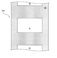
- FIG. 1A is an exploded perspective view of the cover component 1 according to Embodiment 1
- FIG. 1B is a plan view thereof
- FIG. 1C is a side sectional view thereof.
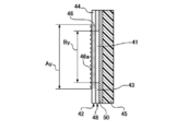
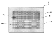
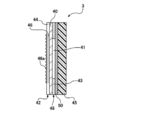
- the cover component 1 is attached to a display panel such as an in-vehicle display device or a mobile device, and includes a hard coat layer 42, a decorative layer 48, an adhesive layer 50, and a transparent base material 45.
- the hard coat layer 42 is a transparent resin layer, for example, a layer of polyethylene terephthalate (PET), and is provided on the outermost surface of the cover component 1.
- PET polyethylene terephthalate
- the hard coat layer 42 overlaps with the decorative layer 48 below the hard coat layer 42.
- the decorative layer 48 includes a frame-shaped colored region 43 and a transmissive region 41 provided inside the colored region.
- the transmissive area 41 is a space for displaying the contents of the display panel.
- the transmissive region 41 may be a translucent material fitted inside the colored region 43.
- An adhesive layer 50 for adhesion to the transparent substrate 45 is provided below the decorative layer 48.
- the thickness of the hard coat layer 42 is, for example, about 5 ⁇ m
- the thickness of the decorative layer 48 is, for example, about several ⁇ m
- the thickness of the adhesive layer 50 is, for example, about 1 to 5 ⁇ m
- the thickness of the transparent substrate 45 is, for example, 2 mm.
- the hard coat layer 42 is composed of an antireflection region 46 and a surrounding region 44, and a fine uneven shape 46 a is provided on the surface of the antireflection region 46.
- the antireflection region 46 is formed so as to cover the transmissive region 41 of the decorative layer 48 and to protrude into the colored region 43 over the entire inner periphery of the colored region 43. That is, in a plan view (when viewed from a direction perpendicular to each layer), the fine concavo-convex shape 46 a overlaps the transmission region 41 and protrudes to the inside of the coloring region 43.
- the surface of the region 44 around the antireflection region 46 has a smooth shape.
- the cover part 1 it is possible to suppress the deterioration of the quality of the cover part.
- the alignment between the antireflection region 46 and the transmission region must be strictly performed. That is, if there is even a slight misalignment between the antireflection area 46 and the transmissive area 41, an area where the antireflection area 46 and the transmissive area 41 do not overlap in a plan view is generated. There was a risk that internal light, for example, light generated from a backlight or an organic EL leaked to the outside and dazzled the viewer. Further, in this non-overlapping region, light outside the display panel, for example, sunlight or illumination light is reflected to cause glare, which may cause glare to the viewer.
- the antireflection region 46 provided with the fine concavo-convex shape 46 a on the surface covers the transmission region 41 and is a colored region over the entire inner periphery of the colored region 43. 43 is formed to protrude. Therefore, even if a positional deviation occurs between the antireflection region 46 and the transmissive region 41, the antireflection region 46 overlaps the transmissive region 41, so that the above-described light leakage and glare can be suppressed. It becomes possible to suppress the deterioration of the quality of parts.
- the transmissive region 41 and the antireflection region 46 have a rectangular shape having a long side and a short side in plan view.
- the length of the long side of the antireflection region 46 is Ax
- the length of the short side is Ay
- the length of the long side inside the colored region 43 is Bx
- the length of the short side is By
- the plan view When the colored region 43 is positioned at the center of the antireflection region 46, 0.05 mm ⁇ (Ax ⁇ Bx) /2 ⁇ 0.25 mm and 0.05 mm ⁇ (Ay ⁇ By) / 2 ⁇ 0. It is preferable to satisfy the condition of 25 mm.
- (Ax ⁇ Bx) / 2 is a dimension in which the antireflection region 46 protrudes into the colored region 43 in the long side direction.
- (Ay ⁇ By) / 2 is a dimension in which the antireflection region 46 protrudes into the colored region 43 in the short side direction.
- the dimension where the antireflection area 46 protrudes into the colored area 43 on each side is less than 0.05 mm, there occurs an area where the antireflection area 46 and the transmission area 41 do not overlap when the cover part 1 is viewed obliquely. There is a risk of light leakage and glare.
- the dimension in which the antireflection region 46 protrudes into the colored region 43 exceeds 0.25 mm, the fine uneven shape 46a is conspicuous in the colored region 43, which causes a design problem. Therefore, it is preferable to satisfy the above conditions.
- the dimensions of the antireflection region 46 protruding from the colored region 43 are exaggerated in order to explain the contents of the present embodiment.
- the fine uneven shape 46a provided on the surface of the antireflection region 46 has an arithmetic average roughness (Ra) of more than 0.08 ⁇ m and less than 0.2 ⁇ m, and a root mean square roughness (Rms) of 80 nm. It is preferably less than 200 nm.
- Ra arithmetic average roughness
- Rms root mean square roughness
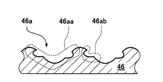
- the fine concavo-convex shape 46a is composed of a concavo-convex shape having two sizes (a first concavo-convex shape 46aa and a second concavo-convex shape 46ab) as shown in FIG.
- the first uneven shape 46aa is provided on the surface of the antireflection region 46
- the second uneven shape 46ab is provided on the surface of the first uneven shape 46aa.
- the first concavo-convex shape 46aa has an arithmetic average roughness (Ra) of about 0.2 ⁇ m (for example, 0.15 ⁇ m or more and 0.25 ⁇ m or less) and a root mean square roughness (Rms) of about 200 nm (for example, 150 nm). More than 250 nm).
- the second uneven shape 46ab has an arithmetic average roughness (Ra) of about 0.08 ⁇ m (for example, 0.07 ⁇ m or more and 0.09 ⁇ m or less), and a root mean square roughness (Rms) of about 80 nm (for example, 70 nm). More than 90 nm).
- the first concavo-convex shape 46aa can ensure the antiglare property, and the second concavo-convex shape 46ab can suppress glare due to pixel interference from the display panel. Can be improved.
- the first concavo-convex shape 46aa if the size of the first concavo-convex shape 46aa is near the pixel size of the display panel, the first concavo-convex shape 46aa functions like a lens so that the pixel There is a risk that glare will occur in the display on the display panel. Therefore, such a glare can be prevented by providing the second concavo-convex shape 46ab on the surface of the first concavo-convex shape 46aa.
- the material of the transparent substrate 45 is a general-purpose molding resin such as a polycarbonate (PC) resin, a polymethyl methacrylate (PMMA) resin, an ABS resin, a polystyrene (PS) resin, or a polyolefin resin.
- PC polycarbonate
- PMMA polymethyl methacrylate
- PS polystyrene
- the material of the adhesive layer 50 is not particularly limited as long as it has good adhesion to the transparent substrate 45.
- the cover component according to this embodiment is not limited to this aspect.
- these shapes may each be circular, and furthermore, these shapes may be different from each other. If the antireflection region 46 covers the transmission region 41 and is formed so as to protrude from the coloring region 43 over the entire inner periphery of the coloring region 43, the problem can be solved.
- the cover component according to the present embodiment is not limited to this aspect.
- the fine uneven shape 46a may be provided on the back surface of the antireflection region 46, that is, on the decorative layer 48 side, or may be provided on both the front surface and the back surface (both surfaces). In other words, it is only necessary that a fine uneven shape is formed on at least one surface of the antireflection region 46.
- the hard coat layer 42 does not include the antireflection region 46, and an antireflection layer including the antireflection region may be provided separately.
- the present embodiment is a mode in which the hard coat layer 42 having the protective function and antifouling function of the display panel also serves as the antireflection layer having the antireflection function.
- Such a cover component may be an embodiment in which the hard coat layer and the antireflection layer are provided separately.
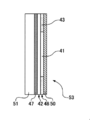
- FIG. 3A is a plan view of a transfer film for manufacturing a cover part according to the present embodiment
- FIG. 3B is a cross-sectional view of the transfer film.
- the transfer film 53 is obtained by laminating a base film 51, a release layer 47, a hard coat layer 42, a decorative layer 48, and an adhesive layer 50 in this order.
- the base film 51 is a belt-like member, and is formed of, for example, polyethylene terephthalate (PET).
- PET polyethylene terephthalate
- the release layer 47 is interposed between the base film 51 and the hard coat layer 42. The release layer 47 makes the hard coat layer 42 easy to release from the base film 51.
- the hard coat layer 42 is preferably an after-curing type that is UV-cured after molding in order to improve the formation of the fine uneven shape.
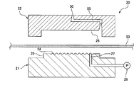
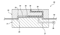
- the cover component according to the present embodiment is manufactured by the insert molding method using the manufacturing apparatus 20, for example.
- the manufacturing apparatus 20 includes a first die 21 having a convex portion 25, a suction hole 27, and a vacuum pump 28, a second die 22 having a concave portion 26, a spool 30, and a hot liner 55, and a film feeding device (not shown). With. When the first mold 21 and the second mold 22 are clamped, as shown in FIG.
- the convex portion 25 enters the concave portion 26 and a cavity 23 is formed between the convex portion 25 and the concave portion 26. . Further, a fine uneven shape 24 is formed on the surface of the convex portion 25.
- the base film 51 faces the fine uneven shape 24, and the adhesive layer 50 (see FIG. 3B) faces the recess 26 of the second mold 22.
- the transfer film 53 is fed by a film feeding device to be positioned between the first mold 21 and the second mold 22. Thereafter, as shown in FIG. 4B, the transfer film 53 is sandwiched and fixed between the first mold 21 and the second mold 22. The transfer film 53 is brought into close contact with the convex portion 25 by sucking the transfer film 53 with the vacuum pump 28 through the suction hole 27 of the first mold 21. Then, the resin 29 is poured into the cavity 23 from the spool 30 of the second mold 22 through the hot runner 55.
- the poured resin 29 then hardens and becomes the transparent base material 45 shown in FIGS. 1A and 1C and adheres to the adhesive layer 50. Finally, by separating the first mold 21 and the second mold 22, the hard coat layer 42 and the release layer 47 shown in FIG. 3B are separated. Thereby, the cover component 1 which concerns on this Embodiment is completed.
- the fine uneven shape 24 of the protrusion 25 is transferred to the hard coat layer 42 through the base film 51 and the release layer 47. According to this manufacturing method, it is possible to obtain the cover component 1 to which the hard coat layer 42, the decorative layer 48, and the like having the fine uneven shape 46a are transferred simultaneously with the formation of the transparent substrate 45.
- FIG. 5 is an enlarged cross-sectional view of the fine concavo-convex shape 24 of the convex portion 25 of the first mold 21.
- a two-step concavo-convex shape of the first concavo-convex shape 32 and the second concavo-convex shape 33 is formed. That is, a first uneven shape 32 is provided on the surface of the convex portion 25, and a second uneven shape 33 is provided on the surface of the first uneven shape 32.
- the following sandblasting method may be mentioned.
- the arithmetic average roughness (Ra) is about 1.2 ⁇ m and squared.
- the first concavo-convex shape 32 having an average roughness (Rms) of about 80 nm can be formed on the surface of the convex portion 25.
- glass beads 34 having a small diameter such as # 320 (average particle diameter 46 ⁇ m) to # 600 (average particle diameter 24 ⁇ m) onto the convex portion 25
- a second mean square roughness (Rms) of about 50 nm is obtained.
- the uneven shape 33 can be formed on the surface of the first uneven shape 32.
- etching or electroforming plating examples include a laser microscope and a surface roughness measuring instrument.
- the cover component 1 of the present embodiment is an aspect in which the decorative layer 48 having the colored region 43 is provided immediately below the hard coat layer 42 having the antireflection region 46, but the cover according to the present embodiment.
- the parts are not limited to this embodiment.
- the transfer film 53 does not include the decorative layer 48, and the decorative layer 48 can be formed by forming the transparent base material 45 by an insert molding method and then printing the transparent base material 45.
- the surface of the antireflection region 46 is composed of two types of fine uneven shapes 46b and 46c.
- the two types of fine concavo-convex shapes 46b and 46c are characterized in that arithmetic mean roughness (Ra) and root mean square roughness (Rms) are different from each other.
- the arithmetic average roughness (Ra) of the upper fine uneven shape 46b is set to the arithmetic average roughness (Ra) of the lower fine uneven shape 46c (
- the root mean square roughness (Rms) of the upper fine uneven shape 46b may be made smaller than the mean square roughness (Rms) of the lower fine uneven shape 46c.
- the upper fine uneven shape 46b has an arithmetic average roughness (Ra) larger than 0.08 ⁇ m and smaller than 0.15 ⁇ m, and The root mean square roughness (Rms) is greater than 80 nm and less than 150 nm.
- the lower fine concavo-convex shape 46c has an arithmetic average roughness (Ra) of greater than 0.08 ⁇ m and less than 0.2 ⁇ m, and a root mean square roughness (Rms) of greater than 80 nm and less than 200 nm.
- 6A and 6B is an aspect in which an upper fine uneven shape 46b and a lower fine uneven shape 46c are provided, but the present embodiment is not limited to this aspect.
- the cover component when the bias of outside light is in the left-right direction, the above effect can be obtained by arranging two types of fine uneven shapes on the left and right.
- the arrangement of fine irregularities should be considered in consideration of the bias of outside light.
- this embodiment is a mode in which two types of fine uneven shapes 46b and 46c are provided
- the cover component according to the present embodiment is not limited to this mode, and arithmetic mean roughness (Ra) and square It may be an embodiment in which three or more types of fine irregularities having different average roughness (Rms) are provided.
- FIGS. 4A and 4B The general configuration of the manufacturing apparatus is the same as that described with reference to FIGS. 4A and 4B in the first embodiment, and a description thereof will be omitted.
- the cross-sectional shape of the fine concavo-convex shape 24 of the convex portion 25 of the first mold 21 is different from the shape of the first embodiment described with reference to FIG.
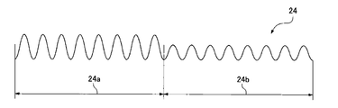
- FIG. 7 is a schematic cross-sectional view of the fine concavo-convex shape 24 of the convex portion 25 of the first mold 21.
- the fine concavo-convex shape 24 is composed of two types of fine concavo-convex shapes 24a and 24b.
- FIG. 7 is a schematic diagram in which the fine uneven shapes 24a and 24b are simplified, and a more detailed shape of the fine uneven shape 24a is shown in FIG. 8A, and a more detailed shape of the fine uneven shape 24b. Is shown in FIG. 8B.
- these two types of fine concavo-convex shapes 24a and 24b are each composed of a two-step concavo-convex shape of a first concavo-convex shape and a second concavo-convex shape.
- the following method may be mentioned.
- the arithmetic mean roughness (Ra) is about 1.2 ⁇ m
- the mean square roughness ( The first concavo-convex shape 32 a having a Rms) of about 80 nm can be formed on a part of the surface of the convex portion 25.
- the arithmetic average roughness (Rms) is about 1.0 ⁇ m by projecting the glass beads 31 b of # 80 onto the portions where the first uneven shape 32 a of the convex portion 25 is not formed.
- the first uneven shape 32b having a root mean square roughness (Rms) of about 70 nm can be formed on the surface of the protrusion 25 where the first uneven shape 32a is not formed.
- the shape 33 can be formed on the surfaces of the first uneven shapes 32a and 32b.
- one type of first uneven shape 32 is provided on the surface of the convex portion 25, but in the second embodiment, the antireflection region of the cover component 2 is provided.
- two types of first types are also provided on the surface of the convex portion 25 of the manufacturing apparatus. Concave and convex shapes 32a and 32b are provided.
- FIG. 9A is a plan view of a cover part according to Embodiment 3
- FIG. 9B is a side sectional view of the cover part.
- detailed description of the same configuration as that of the first embodiment will be omitted, and only different points will be referred to.
- the cover component 3 according to Embodiment 3 includes a chromaticity adjustment layer 40 between the hard coat layer 42 and the decoration layer 48.
- the thickness of the chromaticity adjustment layer 40 is formed with several ⁇ m.
- the chromaticity adjustment layer 40 includes a very small amount of yellow pigment (pigment, dye).
- the light diffused by the fine unevenness 46a on the surface of the antireflection region 46 is more easily reflected as the wavelength is shorter. For this reason, bluish tint occurs when light having a short wavelength such as blue enters the eyes of the viewer.
- the present embodiment includes the chromaticity adjustment layer 40 containing a yellow pigment, the chromaticity adjustment layer 40 supplements the yellow color even when blue light is easily reflected due to aging of the cover component. By doing so, it is possible to cancel the colors. Therefore, even if the cover part deteriorates over time in a place where the external light is strong, such as in a car or a mobile device, a neutral color tone can be maintained.
- the chromaticity adjusting layer 40 preferably contains a UV absorber in addition to the yellow pigment.
- the UV absorber can improve the weather resistance of the transparent base material 45 serving as the base and the display panel itself, and can prevent the attack of the resin on the molecular complex by ultraviolet rays. Therefore, it is possible to prevent the light absorption band of the resin from shifting to the long wavelength side due to aging deterioration and to have absorption in the blue region, and to further maintain the neutral color tone.
- FIGS. 9A and 9B a mode in which one type of fine uneven shape 46 a is provided on the surface of the hard coat layer 42 is illustrated, but the cover component according to the present embodiment is not limited to this mode. That is, as in the second embodiment, a mode in which two or more kinds of fine uneven shapes are provided on the surface of the hard coat layer 42 may be employed.
- FIGS. 10A and 10B show an example of a transfer film 53a used for manufacturing the cover part 3 according to the present embodiment.
- a chromaticity adjusting layer 40 is provided between the hard coat layer 42 and the decorative layer 48.
- the chromaticity adjustment layer 40 is also formed by vacuum film formation, gravure printing, screen printing, ink jet printing, or the like.
- the present disclosure is useful for a cover part that covers the surface of a display panel such as an in-vehicle display device or a mobile device.
Landscapes
- Physics & Mathematics (AREA)
- General Physics & Mathematics (AREA)
- Optics & Photonics (AREA)
- Engineering & Computer Science (AREA)
- Theoretical Computer Science (AREA)
- Health & Medical Sciences (AREA)
- Toxicology (AREA)
- Devices For Indicating Variable Information By Combining Individual Elements (AREA)
- Optical Elements Other Than Lenses (AREA)
- Optical Filters (AREA)
- Surface Treatment Of Optical Elements (AREA)
- Electroluminescent Light Sources (AREA)
Abstract
La présente invention concerne un élément de revêtement destiné à recouvrir la surface d'un panneau d'affichage, pourvu d'une couche décorative configurée à partir d'une région de couleur en forme de cadre et d'une région de transmission disposée sur le côté interne de la région de couleur. L'élément de revêtement comprend également une couche anti-reflet comprenant une région anti-reflet pourvue d'au moins une surface sur laquelle est formée une forme irrégulière fine. La couche antireflet recouvre la couche décorative. La région anti-reflet recouvre la région de transmission et s'étend au-delà de la région de couleur sur toute sa périphérie interne.
Priority Applications (3)
| Application Number | Priority Date | Filing Date | Title |
|---|---|---|---|
| US16/094,219 US20190094419A1 (en) | 2016-05-17 | 2017-04-04 | Cover component and transfer film |
| CN201780028982.7A CN109074764A (zh) | 2016-05-17 | 2017-04-04 | 盖部件以及转印膜 |
| EP17799043.9A EP3460783A4 (fr) | 2016-05-17 | 2017-04-04 | Élément de revêtement et filtre de transfert |
Applications Claiming Priority (2)
| Application Number | Priority Date | Filing Date | Title |
|---|---|---|---|
| JP2016098347A JP2017207563A (ja) | 2016-05-17 | 2016-05-17 | カバー部品、及び転写フィルム |
| JP2016-098347 | 2016-05-17 |
Publications (1)
| Publication Number | Publication Date |
|---|---|
| WO2017199609A1 true WO2017199609A1 (fr) | 2017-11-23 |
Family
ID=60324890
Family Applications (1)
| Application Number | Title | Priority Date | Filing Date |
|---|---|---|---|
| PCT/JP2017/014054 WO2017199609A1 (fr) | 2016-05-17 | 2017-04-04 | Élément de revêtement et filtre de transfert |
Country Status (5)
| Country | Link |
|---|---|
| US (1) | US20190094419A1 (fr) |
| EP (1) | EP3460783A4 (fr) |
| JP (1) | JP2017207563A (fr) |
| CN (1) | CN109074764A (fr) |
| WO (1) | WO2017199609A1 (fr) |
Families Citing this family (2)
| Publication number | Priority date | Publication date | Assignee | Title |
|---|---|---|---|---|
| JP2019101295A (ja) * | 2017-12-05 | 2019-06-24 | Nissha株式会社 | 加飾成形品の製造方法、加飾成形品の製造装置及び加飾成形品 |
| CN114236710A (zh) * | 2021-12-13 | 2022-03-25 | 无锡鑫巨宏智能科技有限公司 | 一种高速耦合透镜 |
Citations (8)
| Publication number | Priority date | Publication date | Assignee | Title |
|---|---|---|---|---|
| JP2002189107A (ja) | 2000-12-21 | 2002-07-05 | Nissha Printing Co Ltd | 反射防止部材 |
| JP2006145736A (ja) * | 2004-11-18 | 2006-06-08 | Konica Minolta Opto Inc | 防眩性反射防止フィルム、偏光板および画像表示装置 |
| JP2008151930A (ja) * | 2006-12-15 | 2008-07-03 | Nof Corp | 転写用反射防止フィルム並びにそれを用いた転写物及び表示装置 |
| US20110228401A1 (en) * | 2008-11-13 | 2011-09-22 | Panasonic Corporation | Optical filter and display device |
| JP2013230652A (ja) | 2012-05-02 | 2013-11-14 | Panasonic Corp | 成形装置および成形方法ならびに成形品 |
| JP2014074810A (ja) * | 2012-10-04 | 2014-04-24 | Nippon Electric Glass Co Ltd | 光学シート及びその製造方法 |
| JP2016035519A (ja) * | 2014-08-04 | 2016-03-17 | パナソニックIpマネジメント株式会社 | パネルユニット、ガラスパネル及びパネル材 |
| JP2016045298A (ja) * | 2014-08-21 | 2016-04-04 | 大日本印刷株式会社 | 表示装置用前面板およびその製造方法 |
Family Cites Families (6)
| Publication number | Priority date | Publication date | Assignee | Title |
|---|---|---|---|---|
| US8672493B2 (en) * | 2009-03-30 | 2014-03-18 | Sharp Kabushiki Kaisha | Display device and optical film |
| WO2013187281A1 (fr) * | 2012-06-11 | 2013-12-19 | シャープ株式会社 | Dispositif d'affichage |
| JP5998882B2 (ja) * | 2012-11-29 | 2016-09-28 | 凸版印刷株式会社 | 転写フィルムおよび転写フィルムの製造方法 |
| CN203480457U (zh) * | 2013-06-14 | 2014-03-12 | 胜华科技股份有限公司 | 装饰盖板及其触控面板 |
| JP2015152658A (ja) * | 2014-02-12 | 2015-08-24 | 住友化学株式会社 | 防眩フィルム |
| JP6275072B2 (ja) * | 2014-08-28 | 2018-02-07 | 富士フイルム株式会社 | 反射防止積層体、偏光板、カバーガラス、画像表示装置、及び反射防止積層体の製造方法 |
-
2016
- 2016-05-17 JP JP2016098347A patent/JP2017207563A/ja active Pending
-
2017
- 2017-04-04 EP EP17799043.9A patent/EP3460783A4/fr active Pending
- 2017-04-04 US US16/094,219 patent/US20190094419A1/en not_active Abandoned
- 2017-04-04 WO PCT/JP2017/014054 patent/WO2017199609A1/fr unknown
- 2017-04-04 CN CN201780028982.7A patent/CN109074764A/zh active Pending
Patent Citations (8)
| Publication number | Priority date | Publication date | Assignee | Title |
|---|---|---|---|---|
| JP2002189107A (ja) | 2000-12-21 | 2002-07-05 | Nissha Printing Co Ltd | 反射防止部材 |
| JP2006145736A (ja) * | 2004-11-18 | 2006-06-08 | Konica Minolta Opto Inc | 防眩性反射防止フィルム、偏光板および画像表示装置 |
| JP2008151930A (ja) * | 2006-12-15 | 2008-07-03 | Nof Corp | 転写用反射防止フィルム並びにそれを用いた転写物及び表示装置 |
| US20110228401A1 (en) * | 2008-11-13 | 2011-09-22 | Panasonic Corporation | Optical filter and display device |
| JP2013230652A (ja) | 2012-05-02 | 2013-11-14 | Panasonic Corp | 成形装置および成形方法ならびに成形品 |
| JP2014074810A (ja) * | 2012-10-04 | 2014-04-24 | Nippon Electric Glass Co Ltd | 光学シート及びその製造方法 |
| JP2016035519A (ja) * | 2014-08-04 | 2016-03-17 | パナソニックIpマネジメント株式会社 | パネルユニット、ガラスパネル及びパネル材 |
| JP2016045298A (ja) * | 2014-08-21 | 2016-04-04 | 大日本印刷株式会社 | 表示装置用前面板およびその製造方法 |
Also Published As
| Publication number | Publication date |
|---|---|
| EP3460783A4 (fr) | 2019-05-22 |
| JP2017207563A (ja) | 2017-11-24 |
| CN109074764A (zh) | 2018-12-21 |
| EP3460783A1 (fr) | 2019-03-27 |
| US20190094419A1 (en) | 2019-03-28 |
Similar Documents
| Publication | Publication Date | Title |
|---|---|---|
| KR102612738B1 (ko) | 디스플레이 장치 | |
| US8672493B2 (en) | Display device and optical film | |
| CN109116621A (zh) | 显示模组和显示装置 | |
| TWI786412B (zh) | 顯示裝置及其製造方法 | |
| US8736960B2 (en) | Structure with observation port | |
| KR102337341B1 (ko) | 차량용 곡면 디스플레이 장치 및 이의 제조방법 | |
| US11426982B2 (en) | Display panel and method of manufacturing the same | |
| WO2008110045A1 (fr) | Film optique utilisé comme lentille | |
| JP7432297B2 (ja) | 表示装置、および、印刷層付き板の製造方法 | |
| US20080218866A1 (en) | Display element | |
| WO2017199609A1 (fr) | Élément de revêtement et filtre de transfert | |
| JP4521089B2 (ja) | 半透過型液晶表示パネルおよびこれの製造方法 | |
| CN106707598A (zh) | 液晶显示面板及其制造方法 | |
| FR3085904A1 (fr) | Element de carrosserie retroeclaire a fort contraste | |
| CN114973989B (zh) | 拼接显示面板和拼接显示器 | |
| WO2015194462A1 (fr) | Film transparent, article imprimé, dispositif d'impression, et unité d'impression | |
| JP3130253U (ja) | バックライトモジュールのフレーム | |
| KR102102751B1 (ko) | 장식필름 | |
| US9469090B2 (en) | Manufacturing method of display | |
| KR100927588B1 (ko) | 평판 디스플레이 장치 | |
| KR101762288B1 (ko) | 필름복합체, 이를 포함하는 표시장치 및 그 제조방법 | |
| US20130077173A1 (en) | Display screen mask structure using shielding frame and manufacturing method thereof | |
| CN108121105A (zh) | 面盖组件、显示模组和移动终端 | |
| US11280950B2 (en) | Backlight module | |
| KR20200083839A (ko) | 저반사 얼비침 방지필름을 이용한 자동차용 디스플레이 구조 |
Legal Events
| Date | Code | Title | Description |
|---|---|---|---|
| NENP | Non-entry into the national phase |
Ref country code: DE |
|
| 121 | Ep: the epo has been informed by wipo that ep was designated in this application |
Ref document number: 17799043 Country of ref document: EP Kind code of ref document: A1 |
|
| ENP | Entry into the national phase |
Ref document number: 2017799043 Country of ref document: EP Effective date: 20181217 |