WO2017199609A1 - Cover component and transfer film - Google Patents
Cover component and transfer film Download PDFInfo
- Publication number
- WO2017199609A1 WO2017199609A1 PCT/JP2017/014054 JP2017014054W WO2017199609A1 WO 2017199609 A1 WO2017199609 A1 WO 2017199609A1 JP 2017014054 W JP2017014054 W JP 2017014054W WO 2017199609 A1 WO2017199609 A1 WO 2017199609A1
- Authority
- WO
- WIPO (PCT)
- Prior art keywords
- region
- layer
- antireflection
- hard coat
- cover component
- Prior art date
Links
- 238000004040 coloring Methods 0.000 claims description 7
- 239000001052 yellow pigment Substances 0.000 claims description 4
- 239000006096 absorbing agent Substances 0.000 claims description 3
- 230000001788 irregular Effects 0.000 abstract 1
- 239000010410 layer Substances 0.000 description 80
- 238000004519 manufacturing process Methods 0.000 description 24
- 230000005540 biological transmission Effects 0.000 description 15
- 230000004313 glare Effects 0.000 description 13
- 239000011347 resin Substances 0.000 description 12
- 229920005989 resin Polymers 0.000 description 12
- 239000000463 material Substances 0.000 description 9
- 239000012790 adhesive layer Substances 0.000 description 8
- 230000006870 function Effects 0.000 description 7
- 239000000758 substrate Substances 0.000 description 7
- 239000011324 bead Substances 0.000 description 6
- 239000011521 glass Substances 0.000 description 6
- 238000000034 method Methods 0.000 description 6
- 238000000465 moulding Methods 0.000 description 5
- 230000015572 biosynthetic process Effects 0.000 description 4
- 230000006866 deterioration Effects 0.000 description 4
- 239000002245 particle Substances 0.000 description 4
- 229920000139 polyethylene terephthalate Polymers 0.000 description 4
- 239000005020 polyethylene terephthalate Substances 0.000 description 4
- 230000032683 aging Effects 0.000 description 3
- 230000003373 anti-fouling effect Effects 0.000 description 3
- 238000009792 diffusion process Methods 0.000 description 3
- 230000009993 protective function Effects 0.000 description 3
- 238000005034 decoration Methods 0.000 description 2
- 230000000694 effects Effects 0.000 description 2
- 238000005755 formation reaction Methods 0.000 description 2
- 238000007646 gravure printing Methods 0.000 description 2
- 238000005286 illumination Methods 0.000 description 2
- 238000007641 inkjet printing Methods 0.000 description 2
- 239000004973 liquid crystal related substance Substances 0.000 description 2
- 230000007935 neutral effect Effects 0.000 description 2
- 229920003229 poly(methyl methacrylate) Polymers 0.000 description 2
- -1 polyethylene terephthalate Polymers 0.000 description 2
- 239000004926 polymethyl methacrylate Substances 0.000 description 2
- 238000007650 screen-printing Methods 0.000 description 2
- 239000004793 Polystyrene Substances 0.000 description 1
- 238000010521 absorption reaction Methods 0.000 description 1
- 229920000122 acrylonitrile butadiene styrene Polymers 0.000 description 1
- 239000003086 colorant Substances 0.000 description 1
- 230000007423 decrease Effects 0.000 description 1
- 238000010586 diagram Methods 0.000 description 1
- 238000005323 electroforming Methods 0.000 description 1
- 238000005530 etching Methods 0.000 description 1
- 238000001746 injection moulding Methods 0.000 description 1
- 238000010030 laminating Methods 0.000 description 1
- 230000031700 light absorption Effects 0.000 description 1
- 230000003287 optical effect Effects 0.000 description 1
- 239000000049 pigment Substances 0.000 description 1
- 238000007747 plating Methods 0.000 description 1
- 239000004417 polycarbonate Substances 0.000 description 1
- 229920000515 polycarbonate Polymers 0.000 description 1
- 229920005672 polyolefin resin Polymers 0.000 description 1
- 238000007639 printing Methods 0.000 description 1
- 239000004576 sand Substances 0.000 description 1
- 238000005488 sandblasting Methods 0.000 description 1
- 239000013589 supplement Substances 0.000 description 1
- 230000003746 surface roughness Effects 0.000 description 1
Images


Classifications
-
- G—PHYSICS
- G02—OPTICS
- G02B—OPTICAL ELEMENTS, SYSTEMS OR APPARATUS
- G02B1/00—Optical elements characterised by the material of which they are made; Optical coatings for optical elements
- G02B1/10—Optical coatings produced by application to, or surface treatment of, optical elements
- G02B1/11—Anti-reflection coatings
- G02B1/118—Anti-reflection coatings having sub-optical wavelength surface structures designed to provide an enhanced transmittance, e.g. moth-eye structures
-
- G—PHYSICS
- G02—OPTICS
- G02B—OPTICAL ELEMENTS, SYSTEMS OR APPARATUS
- G02B1/00—Optical elements characterised by the material of which they are made; Optical coatings for optical elements
- G02B1/10—Optical coatings produced by application to, or surface treatment of, optical elements
-
- G—PHYSICS
- G02—OPTICS
- G02B—OPTICAL ELEMENTS, SYSTEMS OR APPARATUS
- G02B1/00—Optical elements characterised by the material of which they are made; Optical coatings for optical elements
- G02B1/10—Optical coatings produced by application to, or surface treatment of, optical elements
- G02B1/14—Protective coatings, e.g. hard coatings
-
- G—PHYSICS
- G02—OPTICS
- G02B—OPTICAL ELEMENTS, SYSTEMS OR APPARATUS
- G02B5/00—Optical elements other than lenses
- G02B5/02—Diffusing elements; Afocal elements
-
- G—PHYSICS
- G02—OPTICS
- G02B—OPTICAL ELEMENTS, SYSTEMS OR APPARATUS
- G02B5/00—Optical elements other than lenses
- G02B5/20—Filters
- G02B5/208—Filters for use with infrared or ultraviolet radiation, e.g. for separating visible light from infrared and/or ultraviolet radiation
-
- G—PHYSICS
- G02—OPTICS
- G02B—OPTICAL ELEMENTS, SYSTEMS OR APPARATUS
- G02B5/00—Optical elements other than lenses
- G02B5/20—Filters
- G02B5/22—Absorbing filters
-
- G—PHYSICS
- G09—EDUCATION; CRYPTOGRAPHY; DISPLAY; ADVERTISING; SEALS
- G09F—DISPLAYING; ADVERTISING; SIGNS; LABELS OR NAME-PLATES; SEALS
- G09F9/00—Indicating arrangements for variable information in which the information is built-up on a support by selection or combination of individual elements
-
- H—ELECTRICITY
- H05—ELECTRIC TECHNIQUES NOT OTHERWISE PROVIDED FOR
- H05B—ELECTRIC HEATING; ELECTRIC LIGHT SOURCES NOT OTHERWISE PROVIDED FOR; CIRCUIT ARRANGEMENTS FOR ELECTRIC LIGHT SOURCES, IN GENERAL
- H05B33/00—Electroluminescent light sources
- H05B33/02—Details
-
- H—ELECTRICITY
- H10—SEMICONDUCTOR DEVICES; ELECTRIC SOLID-STATE DEVICES NOT OTHERWISE PROVIDED FOR
- H10K—ORGANIC ELECTRIC SOLID-STATE DEVICES
- H10K50/00—Organic light-emitting devices
Definitions
- the present disclosure relates to a cover component that covers the surface of a display panel such as an in-vehicle display device or a mobile device, and a transfer film used for manufacturing the cover component.
- Such a cover component has a structure in which, for example, a hard coat layer having a protective function and an antifouling function for a display panel and a decorative layer having a decorative function are provided on a transparent substrate.
- the decorative layer is composed of a frame-shaped colored layer and a transmission region provided inside the colored region.
- the transmissive area is a space for displaying the contents of the display panel, and the colored area is an area for giving a design to the edge of the display panel.
- the light generated from the inside of the display panel for example, the light generated from the backlight of the liquid crystal panel or the organic EL panel itself may pass through the transmission region and cause glare to the viewer. Further, light outside the display panel, such as sunlight or illumination light, may be reflected on the surface of the cover component to give glare (also referred to as glare) to the viewer.
- glare also referred to as glare
- the hard coat layer it is conceivable that a fine uneven shape is provided on the surface of the region overlapping the transmission region of the decorative layer.
- a fine irregularity By providing fine irregularities on the surface of the hard coat layer, the light from the inside of the display panel side and the light from the outside of the display panel can be diffused by the hard coat layer. It becomes possible to suppress the dazzling given.
- the cover component according to the present disclosure is a cover component that covers the surface of a display panel, and includes a decorative layer composed of a frame-shaped colored region and a transmissive region provided inside the colored region, and at least one side An antireflection layer including an antireflection region in which a fine uneven shape is formed, and the antireflection layer overlaps the decorative layer, the antireflection region covers the transmission region, and It protrudes to the colored region over the entire inner periphery of the colored region.
- the cover component according to the present disclosure is formed so that the antireflection region having a fine unevenness formed on at least one surface covers the transmission region and protrudes into the coloring region over the entire inner periphery of the coloring region. For this reason, even if a misalignment occurs between the antireflection area and the transmission area, the antireflection area overlaps the transmission area, so that the above-described light leakage and glare can be suppressed, and as a result, the quality of the cover parts decreases. Can be suppressed.
- FIG. 1A is an exploded perspective view of a cover part according to Embodiment 1.
- FIG. 1B is a plan view of the cover part according to Embodiment 1.
- FIG. 1C is a side cross-sectional view of the cover component according to Embodiment 1.
- FIG. 2 is an enlarged cross-sectional view illustrating a preferable aspect of the fine uneven shape of the cover component according to the first embodiment.
- 3A is a plan view of a transfer film used for manufacturing the cover component according to Embodiment 1.
- FIG. 3B is a side cross-sectional view of the transfer film according to Embodiment 1.
- FIG. 4A is a side cross-sectional view of the cover part manufacturing apparatus according to Embodiment 1.
- FIG. 4B is a side cross-sectional view of the manufacturing apparatus according to Embodiment 1.
- FIG. FIG. 5 is an enlarged cross-sectional view illustrating a preferable aspect of the fine uneven shape of the manufacturing apparatus according to the first embodiment.
- 6A is a plan view of a cover component according to Embodiment 2.
- FIG. 6B is a side cross-sectional view of the cover component according to Embodiment 2.
- FIG. 7 is a schematic cross-sectional view of a fine concavo-convex shape of the cover component manufacturing apparatus according to the second embodiment.
- FIG. 8A is an enlarged cross-sectional view illustrating a preferable aspect of the fine uneven shape of the manufacturing apparatus according to Embodiment 2.
- FIG. 8B is an enlarged cross-sectional view showing a preferable aspect of the fine uneven shape of the manufacturing apparatus according to Embodiment 2.
- FIG. 9A is a plan view of a cover part according to Embodiment 3.
- FIG. 9B is a side cross-sectional view of the cover part according to Embodiment 3.
- FIG. 10A is a plan view of a transfer film used for manufacturing a cover part according to Embodiment 3.
- FIG. FIG. 10B is a side cross-sectional view of the transfer film according to Embodiment 3.
- a hard coat layer having a protective function and an antifouling function for a display panel in a mode in which a fine concavo-convex shape is provided only in a region overlapping with the transmissive region, alignment between the fine concavo-convex shape and the transmissive region must be strictly performed. . That is, if there is even a slight misalignment between the fine concavo-convex shape and the transmissive region, a region where the fine concavo-convex shape and the transmissive region do not overlap in a plan view is generated, and light inside the display panel is transmitted from this non-overlapping region. There was a risk of leaking to the outside and dazzling the viewer. (Hereinafter, leakage of light inside the display panel to the outside in this way is simply referred to as “light leakage”.) In addition, in this non-overlapping region, the light outside the display panel reflects and glare. This may cause dazzling to the viewer.
- This disclosure is intended to suppress deterioration in the quality of display panel cover parts due to light leakage and glare.
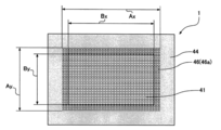
- FIG. 1A is an exploded perspective view of the cover component 1 according to Embodiment 1
- FIG. 1B is a plan view thereof
- FIG. 1C is a side sectional view thereof.
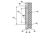
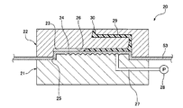
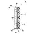
- the cover component 1 is attached to a display panel such as an in-vehicle display device or a mobile device, and includes a hard coat layer 42, a decorative layer 48, an adhesive layer 50, and a transparent base material 45.
- the hard coat layer 42 is a transparent resin layer, for example, a layer of polyethylene terephthalate (PET), and is provided on the outermost surface of the cover component 1.
- PET polyethylene terephthalate
- the hard coat layer 42 overlaps with the decorative layer 48 below the hard coat layer 42.
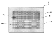
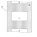
- the decorative layer 48 includes a frame-shaped colored region 43 and a transmissive region 41 provided inside the colored region.
- the transmissive area 41 is a space for displaying the contents of the display panel.
- the transmissive region 41 may be a translucent material fitted inside the colored region 43.
- An adhesive layer 50 for adhesion to the transparent substrate 45 is provided below the decorative layer 48.
- the thickness of the hard coat layer 42 is, for example, about 5 ⁇ m
- the thickness of the decorative layer 48 is, for example, about several ⁇ m
- the thickness of the adhesive layer 50 is, for example, about 1 to 5 ⁇ m
- the thickness of the transparent substrate 45 is, for example, 2 mm.
- the hard coat layer 42 is composed of an antireflection region 46 and a surrounding region 44, and a fine uneven shape 46 a is provided on the surface of the antireflection region 46.
- the antireflection region 46 is formed so as to cover the transmissive region 41 of the decorative layer 48 and to protrude into the colored region 43 over the entire inner periphery of the colored region 43. That is, in a plan view (when viewed from a direction perpendicular to each layer), the fine concavo-convex shape 46 a overlaps the transmission region 41 and protrudes to the inside of the coloring region 43.
- the surface of the region 44 around the antireflection region 46 has a smooth shape.
- the cover part 1 it is possible to suppress the deterioration of the quality of the cover part.
- the alignment between the antireflection region 46 and the transmission region must be strictly performed. That is, if there is even a slight misalignment between the antireflection area 46 and the transmissive area 41, an area where the antireflection area 46 and the transmissive area 41 do not overlap in a plan view is generated. There was a risk that internal light, for example, light generated from a backlight or an organic EL leaked to the outside and dazzled the viewer. Further, in this non-overlapping region, light outside the display panel, for example, sunlight or illumination light is reflected to cause glare, which may cause glare to the viewer.
- the antireflection region 46 provided with the fine concavo-convex shape 46 a on the surface covers the transmission region 41 and is a colored region over the entire inner periphery of the colored region 43. 43 is formed to protrude. Therefore, even if a positional deviation occurs between the antireflection region 46 and the transmissive region 41, the antireflection region 46 overlaps the transmissive region 41, so that the above-described light leakage and glare can be suppressed. It becomes possible to suppress the deterioration of the quality of parts.
- the transmissive region 41 and the antireflection region 46 have a rectangular shape having a long side and a short side in plan view.
- the length of the long side of the antireflection region 46 is Ax
- the length of the short side is Ay
- the length of the long side inside the colored region 43 is Bx
- the length of the short side is By
- the plan view When the colored region 43 is positioned at the center of the antireflection region 46, 0.05 mm ⁇ (Ax ⁇ Bx) /2 ⁇ 0.25 mm and 0.05 mm ⁇ (Ay ⁇ By) / 2 ⁇ 0. It is preferable to satisfy the condition of 25 mm.
- (Ax ⁇ Bx) / 2 is a dimension in which the antireflection region 46 protrudes into the colored region 43 in the long side direction.
- (Ay ⁇ By) / 2 is a dimension in which the antireflection region 46 protrudes into the colored region 43 in the short side direction.
- the dimension where the antireflection area 46 protrudes into the colored area 43 on each side is less than 0.05 mm, there occurs an area where the antireflection area 46 and the transmission area 41 do not overlap when the cover part 1 is viewed obliquely. There is a risk of light leakage and glare.
- the dimension in which the antireflection region 46 protrudes into the colored region 43 exceeds 0.25 mm, the fine uneven shape 46a is conspicuous in the colored region 43, which causes a design problem. Therefore, it is preferable to satisfy the above conditions.
- the dimensions of the antireflection region 46 protruding from the colored region 43 are exaggerated in order to explain the contents of the present embodiment.
- the fine uneven shape 46a provided on the surface of the antireflection region 46 has an arithmetic average roughness (Ra) of more than 0.08 ⁇ m and less than 0.2 ⁇ m, and a root mean square roughness (Rms) of 80 nm. It is preferably less than 200 nm.
- Ra arithmetic average roughness
- Rms root mean square roughness
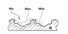
- the fine concavo-convex shape 46a is composed of a concavo-convex shape having two sizes (a first concavo-convex shape 46aa and a second concavo-convex shape 46ab) as shown in FIG.
- the first uneven shape 46aa is provided on the surface of the antireflection region 46
- the second uneven shape 46ab is provided on the surface of the first uneven shape 46aa.
- the first concavo-convex shape 46aa has an arithmetic average roughness (Ra) of about 0.2 ⁇ m (for example, 0.15 ⁇ m or more and 0.25 ⁇ m or less) and a root mean square roughness (Rms) of about 200 nm (for example, 150 nm). More than 250 nm).
- the second uneven shape 46ab has an arithmetic average roughness (Ra) of about 0.08 ⁇ m (for example, 0.07 ⁇ m or more and 0.09 ⁇ m or less), and a root mean square roughness (Rms) of about 80 nm (for example, 70 nm). More than 90 nm).
- the first concavo-convex shape 46aa can ensure the antiglare property, and the second concavo-convex shape 46ab can suppress glare due to pixel interference from the display panel. Can be improved.
- the first concavo-convex shape 46aa if the size of the first concavo-convex shape 46aa is near the pixel size of the display panel, the first concavo-convex shape 46aa functions like a lens so that the pixel There is a risk that glare will occur in the display on the display panel. Therefore, such a glare can be prevented by providing the second concavo-convex shape 46ab on the surface of the first concavo-convex shape 46aa.
- the material of the transparent substrate 45 is a general-purpose molding resin such as a polycarbonate (PC) resin, a polymethyl methacrylate (PMMA) resin, an ABS resin, a polystyrene (PS) resin, or a polyolefin resin.
- PC polycarbonate
- PMMA polymethyl methacrylate
- PS polystyrene
- the material of the adhesive layer 50 is not particularly limited as long as it has good adhesion to the transparent substrate 45.
- the cover component according to this embodiment is not limited to this aspect.
- these shapes may each be circular, and furthermore, these shapes may be different from each other. If the antireflection region 46 covers the transmission region 41 and is formed so as to protrude from the coloring region 43 over the entire inner periphery of the coloring region 43, the problem can be solved.
- the cover component according to the present embodiment is not limited to this aspect.
- the fine uneven shape 46a may be provided on the back surface of the antireflection region 46, that is, on the decorative layer 48 side, or may be provided on both the front surface and the back surface (both surfaces). In other words, it is only necessary that a fine uneven shape is formed on at least one surface of the antireflection region 46.
- the hard coat layer 42 does not include the antireflection region 46, and an antireflection layer including the antireflection region may be provided separately.
- the present embodiment is a mode in which the hard coat layer 42 having the protective function and antifouling function of the display panel also serves as the antireflection layer having the antireflection function.
- Such a cover component may be an embodiment in which the hard coat layer and the antireflection layer are provided separately.
- FIG. 3A is a plan view of a transfer film for manufacturing a cover part according to the present embodiment
- FIG. 3B is a cross-sectional view of the transfer film.
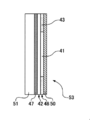
- the transfer film 53 is obtained by laminating a base film 51, a release layer 47, a hard coat layer 42, a decorative layer 48, and an adhesive layer 50 in this order.
- the base film 51 is a belt-like member, and is formed of, for example, polyethylene terephthalate (PET).
- PET polyethylene terephthalate
- the release layer 47 is interposed between the base film 51 and the hard coat layer 42. The release layer 47 makes the hard coat layer 42 easy to release from the base film 51.
- the hard coat layer 42 is preferably an after-curing type that is UV-cured after molding in order to improve the formation of the fine uneven shape.
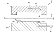
- the cover component according to the present embodiment is manufactured by the insert molding method using the manufacturing apparatus 20, for example.
- the manufacturing apparatus 20 includes a first die 21 having a convex portion 25, a suction hole 27, and a vacuum pump 28, a second die 22 having a concave portion 26, a spool 30, and a hot liner 55, and a film feeding device (not shown). With. When the first mold 21 and the second mold 22 are clamped, as shown in FIG.
- the convex portion 25 enters the concave portion 26 and a cavity 23 is formed between the convex portion 25 and the concave portion 26. . Further, a fine uneven shape 24 is formed on the surface of the convex portion 25.
- the base film 51 faces the fine uneven shape 24, and the adhesive layer 50 (see FIG. 3B) faces the recess 26 of the second mold 22.
- the transfer film 53 is fed by a film feeding device to be positioned between the first mold 21 and the second mold 22. Thereafter, as shown in FIG. 4B, the transfer film 53 is sandwiched and fixed between the first mold 21 and the second mold 22. The transfer film 53 is brought into close contact with the convex portion 25 by sucking the transfer film 53 with the vacuum pump 28 through the suction hole 27 of the first mold 21. Then, the resin 29 is poured into the cavity 23 from the spool 30 of the second mold 22 through the hot runner 55.
- the poured resin 29 then hardens and becomes the transparent base material 45 shown in FIGS. 1A and 1C and adheres to the adhesive layer 50. Finally, by separating the first mold 21 and the second mold 22, the hard coat layer 42 and the release layer 47 shown in FIG. 3B are separated. Thereby, the cover component 1 which concerns on this Embodiment is completed.
- the fine uneven shape 24 of the protrusion 25 is transferred to the hard coat layer 42 through the base film 51 and the release layer 47. According to this manufacturing method, it is possible to obtain the cover component 1 to which the hard coat layer 42, the decorative layer 48, and the like having the fine uneven shape 46a are transferred simultaneously with the formation of the transparent substrate 45.
- FIG. 5 is an enlarged cross-sectional view of the fine concavo-convex shape 24 of the convex portion 25 of the first mold 21.
- a two-step concavo-convex shape of the first concavo-convex shape 32 and the second concavo-convex shape 33 is formed. That is, a first uneven shape 32 is provided on the surface of the convex portion 25, and a second uneven shape 33 is provided on the surface of the first uneven shape 32.
- the following sandblasting method may be mentioned.
- the arithmetic average roughness (Ra) is about 1.2 ⁇ m and squared.
- the first concavo-convex shape 32 having an average roughness (Rms) of about 80 nm can be formed on the surface of the convex portion 25.
- glass beads 34 having a small diameter such as # 320 (average particle diameter 46 ⁇ m) to # 600 (average particle diameter 24 ⁇ m) onto the convex portion 25
- a second mean square roughness (Rms) of about 50 nm is obtained.
- the uneven shape 33 can be formed on the surface of the first uneven shape 32.
- etching or electroforming plating examples include a laser microscope and a surface roughness measuring instrument.
- the cover component 1 of the present embodiment is an aspect in which the decorative layer 48 having the colored region 43 is provided immediately below the hard coat layer 42 having the antireflection region 46, but the cover according to the present embodiment.
- the parts are not limited to this embodiment.
- the transfer film 53 does not include the decorative layer 48, and the decorative layer 48 can be formed by forming the transparent base material 45 by an insert molding method and then printing the transparent base material 45.
- the surface of the antireflection region 46 is composed of two types of fine uneven shapes 46b and 46c.
- the two types of fine concavo-convex shapes 46b and 46c are characterized in that arithmetic mean roughness (Ra) and root mean square roughness (Rms) are different from each other.
- the arithmetic average roughness (Ra) of the upper fine uneven shape 46b is set to the arithmetic average roughness (Ra) of the lower fine uneven shape 46c (
- the root mean square roughness (Rms) of the upper fine uneven shape 46b may be made smaller than the mean square roughness (Rms) of the lower fine uneven shape 46c.
- the upper fine uneven shape 46b has an arithmetic average roughness (Ra) larger than 0.08 ⁇ m and smaller than 0.15 ⁇ m, and The root mean square roughness (Rms) is greater than 80 nm and less than 150 nm.
- the lower fine concavo-convex shape 46c has an arithmetic average roughness (Ra) of greater than 0.08 ⁇ m and less than 0.2 ⁇ m, and a root mean square roughness (Rms) of greater than 80 nm and less than 200 nm.
- 6A and 6B is an aspect in which an upper fine uneven shape 46b and a lower fine uneven shape 46c are provided, but the present embodiment is not limited to this aspect.
- the cover component when the bias of outside light is in the left-right direction, the above effect can be obtained by arranging two types of fine uneven shapes on the left and right.
- the arrangement of fine irregularities should be considered in consideration of the bias of outside light.
- this embodiment is a mode in which two types of fine uneven shapes 46b and 46c are provided
- the cover component according to the present embodiment is not limited to this mode, and arithmetic mean roughness (Ra) and square It may be an embodiment in which three or more types of fine irregularities having different average roughness (Rms) are provided.
- FIGS. 4A and 4B The general configuration of the manufacturing apparatus is the same as that described with reference to FIGS. 4A and 4B in the first embodiment, and a description thereof will be omitted.
- the cross-sectional shape of the fine concavo-convex shape 24 of the convex portion 25 of the first mold 21 is different from the shape of the first embodiment described with reference to FIG.
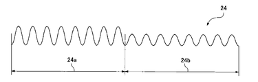
- FIG. 7 is a schematic cross-sectional view of the fine concavo-convex shape 24 of the convex portion 25 of the first mold 21.
- the fine concavo-convex shape 24 is composed of two types of fine concavo-convex shapes 24a and 24b.
- FIG. 7 is a schematic diagram in which the fine uneven shapes 24a and 24b are simplified, and a more detailed shape of the fine uneven shape 24a is shown in FIG. 8A, and a more detailed shape of the fine uneven shape 24b. Is shown in FIG. 8B.
- these two types of fine concavo-convex shapes 24a and 24b are each composed of a two-step concavo-convex shape of a first concavo-convex shape and a second concavo-convex shape.
- the following method may be mentioned.
- the arithmetic mean roughness (Ra) is about 1.2 ⁇ m
- the mean square roughness ( The first concavo-convex shape 32 a having a Rms) of about 80 nm can be formed on a part of the surface of the convex portion 25.
- the arithmetic average roughness (Rms) is about 1.0 ⁇ m by projecting the glass beads 31 b of # 80 onto the portions where the first uneven shape 32 a of the convex portion 25 is not formed.
- the first uneven shape 32b having a root mean square roughness (Rms) of about 70 nm can be formed on the surface of the protrusion 25 where the first uneven shape 32a is not formed.
- the shape 33 can be formed on the surfaces of the first uneven shapes 32a and 32b.
- one type of first uneven shape 32 is provided on the surface of the convex portion 25, but in the second embodiment, the antireflection region of the cover component 2 is provided.
- two types of first types are also provided on the surface of the convex portion 25 of the manufacturing apparatus. Concave and convex shapes 32a and 32b are provided.
- FIG. 9A is a plan view of a cover part according to Embodiment 3
- FIG. 9B is a side sectional view of the cover part.
- detailed description of the same configuration as that of the first embodiment will be omitted, and only different points will be referred to.
- the cover component 3 according to Embodiment 3 includes a chromaticity adjustment layer 40 between the hard coat layer 42 and the decoration layer 48.
- the thickness of the chromaticity adjustment layer 40 is formed with several ⁇ m.
- the chromaticity adjustment layer 40 includes a very small amount of yellow pigment (pigment, dye).
- the light diffused by the fine unevenness 46a on the surface of the antireflection region 46 is more easily reflected as the wavelength is shorter. For this reason, bluish tint occurs when light having a short wavelength such as blue enters the eyes of the viewer.
- the present embodiment includes the chromaticity adjustment layer 40 containing a yellow pigment, the chromaticity adjustment layer 40 supplements the yellow color even when blue light is easily reflected due to aging of the cover component. By doing so, it is possible to cancel the colors. Therefore, even if the cover part deteriorates over time in a place where the external light is strong, such as in a car or a mobile device, a neutral color tone can be maintained.
- the chromaticity adjusting layer 40 preferably contains a UV absorber in addition to the yellow pigment.
- the UV absorber can improve the weather resistance of the transparent base material 45 serving as the base and the display panel itself, and can prevent the attack of the resin on the molecular complex by ultraviolet rays. Therefore, it is possible to prevent the light absorption band of the resin from shifting to the long wavelength side due to aging deterioration and to have absorption in the blue region, and to further maintain the neutral color tone.
- FIGS. 9A and 9B a mode in which one type of fine uneven shape 46 a is provided on the surface of the hard coat layer 42 is illustrated, but the cover component according to the present embodiment is not limited to this mode. That is, as in the second embodiment, a mode in which two or more kinds of fine uneven shapes are provided on the surface of the hard coat layer 42 may be employed.
- FIGS. 10A and 10B show an example of a transfer film 53a used for manufacturing the cover part 3 according to the present embodiment.
- a chromaticity adjusting layer 40 is provided between the hard coat layer 42 and the decorative layer 48.
- the chromaticity adjustment layer 40 is also formed by vacuum film formation, gravure printing, screen printing, ink jet printing, or the like.
- the present disclosure is useful for a cover part that covers the surface of a display panel such as an in-vehicle display device or a mobile device.
Landscapes
- Physics & Mathematics (AREA)
- General Physics & Mathematics (AREA)
- Optics & Photonics (AREA)
- Engineering & Computer Science (AREA)
- Theoretical Computer Science (AREA)
- Health & Medical Sciences (AREA)
- Toxicology (AREA)
- Devices For Indicating Variable Information By Combining Individual Elements (AREA)
- Optical Elements Other Than Lenses (AREA)
- Optical Filters (AREA)
- Surface Treatment Of Optical Elements (AREA)
- Electroluminescent Light Sources (AREA)
Abstract
This cover component for covering the surface of a display panel is provided with a decorative layer configured from a frame-shaped color region and a transmissive region disposed on the inner side of the color region. The cover component also includes an anti-reflection layer including an anti-reflection region with at least one surface having a fine irregular shape formed thereon. The anti-reflection layer overlaps the decorative layer. The anti-reflection region covers the transmissive region and extends past the color region along the entire inner periphery thereof.
Description
本開示は、車載表示機器、モバイル機器などのディスプレイ用パネルの表面を覆うカバー部品、及びそのカバー部品の製造に用いられる転写フィルムに関するものである。
The present disclosure relates to a cover component that covers the surface of a display panel such as an in-vehicle display device or a mobile device, and a transfer film used for manufacturing the cover component.
従来より、ディスプレイ表示機能を持つ車載機器やモバイル機器等において、液晶パネルや有機ELパネル等のディスプレイ用パネルの表面を保護したり、防汚したり、または、ディスプレイ用パネルの縁部を加飾したりすることを目的として、カバー部品が使用されている(例えば、特許文献1、2)。
Conventionally, in in-vehicle devices and mobile devices that have a display display function, the surface of display panels such as liquid crystal panels and organic EL panels are protected or soiled, or the edges of display panels are decorated. Cover parts are used for the purpose (for example, Patent Documents 1 and 2).
このようなカバー部品は、例えば、ディスプレイ用パネルの保護機能及び防汚機能を有するハードコート層と、加飾機能を有する加飾層とが、透明基材上に設けられる構成となっている。加飾層は、枠状の着色層と、この着色領域の内側に設けられた透過領域とで構成されている。透過領域は、ディスプレイ用パネルの内容を表示させるための空間であって、着色領域は、ディスプレイ用パネルの縁部にデザインを付与するための領域である。
Such a cover component has a structure in which, for example, a hard coat layer having a protective function and an antifouling function for a display panel and a decorative layer having a decorative function are provided on a transparent substrate. The decorative layer is composed of a frame-shaped colored layer and a transmission region provided inside the colored region. The transmissive area is a space for displaying the contents of the display panel, and the colored area is an area for giving a design to the edge of the display panel.
ここで、ディスプレイ用パネルの内部から生じた光、例えば、液晶パネルのバックライトや有機ELパネル自身から生じた光は、透過領域を通過して視認者に眩惑を生じさせるおそれがある。また、ディスプレイ用パネルの外部の光、例えば太陽光や照明光等が、カバー部品の表面で反射することによって視認者にギラツキ(グレアとも称される)を与えることがある。
Here, the light generated from the inside of the display panel, for example, the light generated from the backlight of the liquid crystal panel or the organic EL panel itself may pass through the transmission region and cause glare to the viewer. Further, light outside the display panel, such as sunlight or illumination light, may be reflected on the surface of the cover component to give glare (also referred to as glare) to the viewer.
そこで、ハードコート層において、加飾層の透過領域と重なる領域の表面に、微細凹凸形状が設けることが考えられる。ハードコート層の表面に微細凹凸形状を設けることによって、ディスプレイ用パネル側の内部からの光、及びディスプレイ用パネルの外部からの光を、ハードコート層で拡散させることができ、ひいては、視認者に与える眩惑を抑制することが可能となる。
Therefore, in the hard coat layer, it is conceivable that a fine uneven shape is provided on the surface of the region overlapping the transmission region of the decorative layer. By providing fine irregularities on the surface of the hard coat layer, the light from the inside of the display panel side and the light from the outside of the display panel can be diffused by the hard coat layer. It becomes possible to suppress the dazzling given.
本開示に係るカバー部品は、ディスプレイ用パネルの表面を覆うカバー部品であって、枠状の着色領域と前記着色領域の内側に設けられた透過領域とで構成された加飾層と、少なくとも片面に微細凹凸形状が形成された反射防止領域を含む反射防止層と、を備え、前記反射防止層は、前記加飾層と重なり合っており、前記反射防止領域は、前記透過領域を覆い、かつ、前記着色領域の内側全周にわたって前記着色領域にはみ出ていることを特徴とする。
The cover component according to the present disclosure is a cover component that covers the surface of a display panel, and includes a decorative layer composed of a frame-shaped colored region and a transmissive region provided inside the colored region, and at least one side An antireflection layer including an antireflection region in which a fine uneven shape is formed, and the antireflection layer overlaps the decorative layer, the antireflection region covers the transmission region, and It protrudes to the colored region over the entire inner periphery of the colored region.
本開示に係るカバー部品によれば、少なくとも片面に微細凹凸形状が形成された反射防止領域が透過領域を覆い、かつ、着色領域の内側全周にわたって着色領域にはみ出すように形成されている。そのため、反射防止領域と透過領域との間で位置ズレが生じても反射防止領域が透過領域をオーバーラップすることにより、前述した光モレやギラツキを抑えることができ、ひいては、カバー部品の品位低下を抑えることが可能となる。
The cover component according to the present disclosure is formed so that the antireflection region having a fine unevenness formed on at least one surface covers the transmission region and protrudes into the coloring region over the entire inner periphery of the coloring region. For this reason, even if a misalignment occurs between the antireflection area and the transmission area, the antireflection area overlaps the transmission area, so that the above-described light leakage and glare can be suppressed, and as a result, the quality of the cover parts decreases. Can be suppressed.
実施の形態の説明に先立ち、従来の技術における問題点を簡単に説明する。
Prior to the description of the embodiment, the problems in the prior art will be briefly described.
ディスプレイ用パネルの保護機能及び防汚機能を有するハードコート層において、透過領域と重なる領域のみに微細凹凸形状を設けた態様では、微細凹凸形状と透過領域との位置合わせを厳密に行わなければならない。すなわち、微細凹凸形状と透過領域との間に少しでも位置ズレがあると、平面視において微細凹凸形状と透過領域とが重ならない領域が生じ、この重ならない領域からディスプレイ用パネルの内部の光が外部に漏れて視認者に眩惑を与えるおそれがあった。(以下、このようにしてディスプレイ用パネルの内部の光が外部に漏れることを、単に「光モレ」と称す。)また、この重ならない領域において、ディスプレイ用パネルの外部の光が反射してギラツキを生じさせ、視認者に眩惑を与えるおそれがあった。
In a hard coat layer having a protective function and an antifouling function for a display panel, in a mode in which a fine concavo-convex shape is provided only in a region overlapping with the transmissive region, alignment between the fine concavo-convex shape and the transmissive region must be strictly performed. . That is, if there is even a slight misalignment between the fine concavo-convex shape and the transmissive region, a region where the fine concavo-convex shape and the transmissive region do not overlap in a plan view is generated, and light inside the display panel is transmitted from this non-overlapping region. There was a risk of leaking to the outside and dazzling the viewer. (Hereinafter, leakage of light inside the display panel to the outside in this way is simply referred to as “light leakage”.) In addition, in this non-overlapping region, the light outside the display panel reflects and glare. This may cause dazzling to the viewer.
本開示は、ディスプレイ用パネルのカバー部品において、光モレやギラツキによる品位低下を抑えることを目的とする。
This disclosure is intended to suppress deterioration in the quality of display panel cover parts due to light leakage and glare.
(実施の形態1)
(1.カバー部品の構成)
以下実施の形態1に係るカバー部品1について、図面を参照しながら説明する。図1Aは、実施の形態1に係るカバー部品1の分解斜視図、図1Bはその平面図、図1Cはその側面断面図である。このカバー部品1は、車載表示機器やモバイル機器などの表示パネルに取り付けられるものであって、ハードコート層42と加飾層48と接着層50と透明基材45とを備える。 (Embodiment 1)
(1. Configuration of cover parts)
The cover component 1 according to Embodiment 1 will be described below with reference to the drawings. 1A is an exploded perspective view of the cover component 1 according to Embodiment 1, FIG. 1B is a plan view thereof, and FIG. 1C is a side sectional view thereof. The cover component 1 is attached to a display panel such as an in-vehicle display device or a mobile device, and includes ahard coat layer 42, a decorative layer 48, an adhesive layer 50, and a transparent base material 45.
(1.カバー部品の構成)
以下実施の形態1に係るカバー部品1について、図面を参照しながら説明する。図1Aは、実施の形態1に係るカバー部品1の分解斜視図、図1Bはその平面図、図1Cはその側面断面図である。このカバー部品1は、車載表示機器やモバイル機器などの表示パネルに取り付けられるものであって、ハードコート層42と加飾層48と接着層50と透明基材45とを備える。 (Embodiment 1)
(1. Configuration of cover parts)
The cover component 1 according to Embodiment 1 will be described below with reference to the drawings. 1A is an exploded perspective view of the cover component 1 according to Embodiment 1, FIG. 1B is a plan view thereof, and FIG. 1C is a side sectional view thereof. The cover component 1 is attached to a display panel such as an in-vehicle display device or a mobile device, and includes a
ハードコート層42は、透明樹脂層、例えば、ポリエチレンテレフタレート(PET)の層であって、カバー部品1の最表面に設けられる。このハードコート層42は、ハードコート層42の下層の加飾層48と重なり合っている。加飾層48は、枠状の着色領域43と、その着色領域の内側に設けられた透過領域41とで構成されている。透過領域41は、ディスプレイ用パネルの内容を表示させるための空間である。ただし、透過領域41は、着色領域43の内側に嵌め込まれた透光性材料であってもよい。
The hard coat layer 42 is a transparent resin layer, for example, a layer of polyethylene terephthalate (PET), and is provided on the outermost surface of the cover component 1. The hard coat layer 42 overlaps with the decorative layer 48 below the hard coat layer 42. The decorative layer 48 includes a frame-shaped colored region 43 and a transmissive region 41 provided inside the colored region. The transmissive area 41 is a space for displaying the contents of the display panel. However, the transmissive region 41 may be a translucent material fitted inside the colored region 43.
加飾層48のさらに下層には、透明基材45との接着のための接着層50が設けられている。ハードコート層42の厚みは、例えば5μm程度で、加飾層48の厚みは、例えば数μm程度で、接着層50の厚みは、例えば1~5μm程度で、透明基材45の厚みは、例えば2mmである。
An adhesive layer 50 for adhesion to the transparent substrate 45 is provided below the decorative layer 48. The thickness of the hard coat layer 42 is, for example, about 5 μm, the thickness of the decorative layer 48 is, for example, about several μm, the thickness of the adhesive layer 50 is, for example, about 1 to 5 μm, and the thickness of the transparent substrate 45 is, for example, 2 mm.
また、ハードコート層42は、反射防止領域46と、その周囲の領域44とで構成されており、反射防止領域46の表面には、微細凹凸形状46aが設けられている。反射防止領域46は、加飾層48の透過領域41を覆い、かつ着色領域43の内側全周にわたって、着色領域43にはみ出すように形成されている。すなわち、平面視で(各層に対して垂直な方向から見たときに)、微細凹凸形状46aは、透過領域41をオーバーラップして、着色領域43の内側にまではみ出るようになっている。反射防止領域46の周囲の領域44の表面は、平滑形状になっている。
Further, the hard coat layer 42 is composed of an antireflection region 46 and a surrounding region 44, and a fine uneven shape 46 a is provided on the surface of the antireflection region 46. The antireflection region 46 is formed so as to cover the transmissive region 41 of the decorative layer 48 and to protrude into the colored region 43 over the entire inner periphery of the colored region 43. That is, in a plan view (when viewed from a direction perpendicular to each layer), the fine concavo-convex shape 46 a overlaps the transmission region 41 and protrudes to the inside of the coloring region 43. The surface of the region 44 around the antireflection region 46 has a smooth shape.
本実施の形態に係るカバー部品1によれば、カバー部品の品位低下を抑えることが可能となる。例えば、ハードコート層42において、透過領域41と重なる領域のみに微細凹凸形状を設けた態様では、反射防止領域46と透過領域との位置合わせを厳密に行わなければならない。すなわち、反射防止領域46と透過領域41との間に少しでも位置ズレがあると、平面視において反射防止領域46と透過領域41とが重ならない領域が生じ、この重ならない領域からディスプレイ用パネルの内部の光、例えばバックライトや有機ELから生じた光が外部に漏れて視認者に眩惑を与えるおそれがあった。また、この重ならない領域において、ディスプレイ用パネルの外部の光、例えば太陽光や照明光が反射してギラツキを生じさせ、視認者に眩惑を与えるおそれがあった。
According to the cover part 1 according to the present embodiment, it is possible to suppress the deterioration of the quality of the cover part. For example, in the aspect in which the fine unevenness is provided only in the region that overlaps with the transmission region 41 in the hard coat layer 42, the alignment between the antireflection region 46 and the transmission region must be strictly performed. That is, if there is even a slight misalignment between the antireflection area 46 and the transmissive area 41, an area where the antireflection area 46 and the transmissive area 41 do not overlap in a plan view is generated. There was a risk that internal light, for example, light generated from a backlight or an organic EL leaked to the outside and dazzled the viewer. Further, in this non-overlapping region, light outside the display panel, for example, sunlight or illumination light is reflected to cause glare, which may cause glare to the viewer.
一方で、本実施の形態に係るカバー部品1によれば、表面に微細凹凸形状46aが設けられた反射防止領域46が、透過領域41を覆い、かつ、着色領域43の内側全周にわたって着色領域43にはみ出すように形成されている。そのため、反射防止領域46と透過領域41との間で位置ズレが生じても反射防止領域46が透過領域41をオーバーラップすることにより、前述した光モレやギラツキを抑えることができ、ひいては、カバー部品の品位低下を抑えることが可能となる。
On the other hand, according to the cover component 1 according to the present embodiment, the antireflection region 46 provided with the fine concavo-convex shape 46 a on the surface covers the transmission region 41 and is a colored region over the entire inner periphery of the colored region 43. 43 is formed to protrude. Therefore, even if a positional deviation occurs between the antireflection region 46 and the transmissive region 41, the antireflection region 46 overlaps the transmissive region 41, so that the above-described light leakage and glare can be suppressed. It becomes possible to suppress the deterioration of the quality of parts.
ここで、本実施の形態においては、透過領域41及び反射防止領域46は、平面視において長辺と短辺を有する長方形状である。そして、反射防止領域46の長辺の長さをAx、短辺の長さをAy、着色領域43の内側の長辺の長さをBx、短辺の長さをByとし、かつ、平面視で着色領域43が反射防止領域46中央に位置することとしたとき、0.05mm≦(Ax-Bx)/2≦0.25mm、かつ、0.05mm≦(Ay-By)/2≦0.25mmの条件を満たすことが好ましい。(Ax-Bx)/2は、長辺方向において、反射防止領域46が着色領域43にはみ出る寸法である。(Ay-By)/2は、短辺方向において、反射防止領域46が着色領域43にはみ出る寸法である。
Here, in the present embodiment, the transmissive region 41 and the antireflection region 46 have a rectangular shape having a long side and a short side in plan view. The length of the long side of the antireflection region 46 is Ax, the length of the short side is Ay, the length of the long side inside the colored region 43 is Bx, the length of the short side is By, and the plan view When the colored region 43 is positioned at the center of the antireflection region 46, 0.05 mm ≦ (Ax−Bx) /2≦0.25 mm and 0.05 mm ≦ (Ay−By) / 2 ≦ 0. It is preferable to satisfy the condition of 25 mm. (Ax−Bx) / 2 is a dimension in which the antireflection region 46 protrudes into the colored region 43 in the long side direction. (Ay−By) / 2 is a dimension in which the antireflection region 46 protrudes into the colored region 43 in the short side direction.
それぞれの辺で反射防止領域46が着色領域43にはみ出る寸法が0.05mm未満の場合、カバー部品1を斜めから見たときに反射防止領域46と透過領域41とが重ならない領域が生じて、光モレやギラツキが生じるおそれがある。一方で、反射防止領域46が着色領域43にはみ出る寸法が0.25mmを超える場合、着色領域43において微細凹凸形状46aが目立ってしまうため、デザイン上の問題がある。したがって、上記条件を満たすことが好ましい。なお、図面においては、本実施の形態の内容を説明するために、反射防止領域46が着色領域43にはみ出る寸法を誇張して描かれている。
When the dimension where the antireflection area 46 protrudes into the colored area 43 on each side is less than 0.05 mm, there occurs an area where the antireflection area 46 and the transmission area 41 do not overlap when the cover part 1 is viewed obliquely. There is a risk of light leakage and glare. On the other hand, when the dimension in which the antireflection region 46 protrudes into the colored region 43 exceeds 0.25 mm, the fine uneven shape 46a is conspicuous in the colored region 43, which causes a design problem. Therefore, it is preferable to satisfy the above conditions. In the drawings, the dimensions of the antireflection region 46 protruding from the colored region 43 are exaggerated in order to explain the contents of the present embodiment.
また、反射防止領域46の表面に設けられた微細凹凸形状46aは、算術平均粗さ(Ra)が0.08μmより大きく0.2μm未満であって、かつ自乗平均粗さ(Rms)が80nmより大きく200nm未満であることが好ましい。算術平均粗さ(Ra)が0.08μm以下の場合、防眩性が低下してしまう一方で、算術平均粗さ(Ra)が0.2μmを超える場合、光の拡散効果が大きくなり、画面の白ボケが発生してしまうためである。また、自乗平均粗さ(Rms)が80nm以下の場合は、防眩性が低下する一方で、自乗平均粗さ(Rms)が200nmを超える場合は、光の拡散が大きくなり、画面の白ボケが発生してしまうためである。
Further, the fine uneven shape 46a provided on the surface of the antireflection region 46 has an arithmetic average roughness (Ra) of more than 0.08 μm and less than 0.2 μm, and a root mean square roughness (Rms) of 80 nm. It is preferably less than 200 nm. When the arithmetic average roughness (Ra) is 0.08 μm or less, the antiglare property is deteriorated. On the other hand, when the arithmetic average roughness (Ra) exceeds 0.2 μm, the light diffusion effect is increased, and the screen This is because of the occurrence of white blur. On the other hand, when the root mean square roughness (Rms) is 80 nm or less, the anti-glare property is deteriorated. On the other hand, when the root mean square roughness (Rms) exceeds 200 nm, the light diffusion becomes large, and the screen is blurred. This is because of this.
また、微細凹凸形状46aは、図2に示すように2段階の大きさの凹凸形状(第1の凹凸形状46aa、第2の凹凸形状46ab)で構成されることが好ましい。図2に示す態様では、第1の凹凸形状46aaは、反射防止領域46の表面に設けられており、第2の凹凸形状46abは、その第1の凹凸形状46aaの表面に設けられている。第1の凹凸形状46aaは、算術平均粗さ(Ra)が0.2μm前後(例えば、0.15μm以上0.25μm以下)で、かつ、自乗平均粗さ(Rms)が200nm前後(例えば、150nm以上250nm以下)である。第2の凹凸形状46abは、算術平均粗さ(Ra)が0.08μm前後(例えば、0.07μm以上0.09μm以下)で、かつ、自乗平均粗さ(Rms)が80nm前後(例えば、70nm以上90nm以下)である。この態様によれば、第1の凹凸形状46aaで防眩性を担保するとともに、第2の凹凸形状46abでディスプレイ用パネルからの画素干渉によるギラツキを抑えることが可能となり、ひいては、カバー部品の品位を向上させることが可能となる。例えば、第1の凹凸形状46aaのみの場合、その第1の凹凸形状46aaのサイズがディスプレイ用パネルの画素サイズ付近であると、第1の凹凸形状46aaがレンズのような働きをして画素が拡大され、ディスプレイ用パネルの表示にギラツキが生じるおそれがある。そこで、第1の凹凸形状46aaの表面に第2の凹凸形状46abが設けられることによって、このようなギラツキを防止することが可能となる。
Moreover, it is preferable that the fine concavo-convex shape 46a is composed of a concavo-convex shape having two sizes (a first concavo-convex shape 46aa and a second concavo-convex shape 46ab) as shown in FIG. In the embodiment shown in FIG. 2, the first uneven shape 46aa is provided on the surface of the antireflection region 46, and the second uneven shape 46ab is provided on the surface of the first uneven shape 46aa. The first concavo-convex shape 46aa has an arithmetic average roughness (Ra) of about 0.2 μm (for example, 0.15 μm or more and 0.25 μm or less) and a root mean square roughness (Rms) of about 200 nm (for example, 150 nm). More than 250 nm). The second uneven shape 46ab has an arithmetic average roughness (Ra) of about 0.08 μm (for example, 0.07 μm or more and 0.09 μm or less), and a root mean square roughness (Rms) of about 80 nm (for example, 70 nm). More than 90 nm). According to this aspect, the first concavo-convex shape 46aa can ensure the antiglare property, and the second concavo-convex shape 46ab can suppress glare due to pixel interference from the display panel. Can be improved. For example, in the case of only the first concavo-convex shape 46aa, if the size of the first concavo-convex shape 46aa is near the pixel size of the display panel, the first concavo-convex shape 46aa functions like a lens so that the pixel There is a risk that glare will occur in the display on the display panel. Therefore, such a glare can be prevented by providing the second concavo-convex shape 46ab on the surface of the first concavo-convex shape 46aa.
なお、透明基材45の材料は、例えば、ポリカーボネート(PC)樹脂、ポリメタクリル酸メチル(PMMA)樹脂、ABS樹脂、ポリスチレン(PS)樹脂、ポリオレフィン系樹脂などの汎用成形樹脂である。また、射出成形を用いず転写やUV露光などを用いる場合は、光学用途の樹脂やスーパーエンジニアリング樹脂など高温で成形が必要な樹脂にも対応可能である。接着層50の材料は、透明基材45と接着性が良いものであれば特に限定されない。
The material of the transparent substrate 45 is a general-purpose molding resin such as a polycarbonate (PC) resin, a polymethyl methacrylate (PMMA) resin, an ABS resin, a polystyrene (PS) resin, or a polyolefin resin. In addition, when transfer, UV exposure, or the like is used without using injection molding, it is possible to deal with resins that require molding at high temperatures, such as resins for optical applications and super engineering resins. The material of the adhesive layer 50 is not particularly limited as long as it has good adhesion to the transparent substrate 45.
ところで、本実施の形態は、透過領域41及び反射防止領域46が、平面視においてそれぞれ長方形状である態様であるが、本実施の形態に係るカバー部品はこの態様に限られない。例えば、これらの形状がそれぞれ円形状であってもよく、さらには、これらの形状が互いに異なる形状であってもよい。反射防止領域46が、透過領域41を覆い、かつ着色領域43の内側全周にわたって、着色領域43にはみ出すように形成されていれば、課題を解決することが可能である。
By the way, although this embodiment is an aspect in which the transmission region 41 and the antireflection region 46 are each rectangular in plan view, the cover component according to this embodiment is not limited to this aspect. For example, these shapes may each be circular, and furthermore, these shapes may be different from each other. If the antireflection region 46 covers the transmission region 41 and is formed so as to protrude from the coloring region 43 over the entire inner periphery of the coloring region 43, the problem can be solved.
また、本実施の形態は、ハードコート層42の反射防止領域46の表面に微細凹凸形状46aが設けられる態様であるが、本実施の形態に係るカバー部品は、この態様に限られない。例えば、微細凹凸形状46aは、反射防止領域46の裏面、すなわち、加飾層48側に設けられてもよく、表面と裏面の両方(両面)に設けられてもよい。いいかえると、反射防止領域46の少なくとも片面に微細凹凸形状が形成されていればよい。
Further, although the present embodiment is an aspect in which the fine uneven shape 46a is provided on the surface of the antireflection region 46 of the hard coat layer 42, the cover component according to the present embodiment is not limited to this aspect. For example, the fine uneven shape 46a may be provided on the back surface of the antireflection region 46, that is, on the decorative layer 48 side, or may be provided on both the front surface and the back surface (both surfaces). In other words, it is only necessary that a fine uneven shape is formed on at least one surface of the antireflection region 46.
さらには、ハードコート層42が反射防止領域46を含まず、反射防止領域を含む反射防止層を別途設けるようにしてもよい。換言すると、本実施の形態は、ディスプレイ用パネルの保護機能及び防汚機能を有するハードコート層42が、反射防止機能を有する反射防止層の役割を兼任する態様であるが、本実施の形態に係るカバー部品は、ハードコート層と反射防止層とが、別個に設けられる態様であってもよい。
Furthermore, the hard coat layer 42 does not include the antireflection region 46, and an antireflection layer including the antireflection region may be provided separately. In other words, the present embodiment is a mode in which the hard coat layer 42 having the protective function and antifouling function of the display panel also serves as the antireflection layer having the antireflection function. Such a cover component may be an embodiment in which the hard coat layer and the antireflection layer are provided separately.
(2.転写フィルムの構成)
図3Aは、本実施の形態に係るカバー部品を製造するための転写フィルムの平面図であり、図3Bは、この転写フィルムの断面図である。転写フィルム53は、ベースフィルム51と、剥離層47と、ハードコート層42と、加飾層48と、接着層50とがこの順番に積層されたものである。 (2. Structure of transfer film)
FIG. 3A is a plan view of a transfer film for manufacturing a cover part according to the present embodiment, and FIG. 3B is a cross-sectional view of the transfer film. Thetransfer film 53 is obtained by laminating a base film 51, a release layer 47, a hard coat layer 42, a decorative layer 48, and an adhesive layer 50 in this order.
図3Aは、本実施の形態に係るカバー部品を製造するための転写フィルムの平面図であり、図3Bは、この転写フィルムの断面図である。転写フィルム53は、ベースフィルム51と、剥離層47と、ハードコート層42と、加飾層48と、接着層50とがこの順番に積層されたものである。 (2. Structure of transfer film)
FIG. 3A is a plan view of a transfer film for manufacturing a cover part according to the present embodiment, and FIG. 3B is a cross-sectional view of the transfer film. The
ベースフィルム51は、帯状部材であって、例えば、ポリエチレンテレフタレート(PET)で形成されている。ハードコート層42、加飾層48、及び接着層50の構成については、カバー部品1の構成と同じであるため、詳細な説明を省略する。剥離層47は、ベースフィルム51とハードコート層42との間に介在する。この剥離層47によって、ハードコート層42はベースフィルム51から離型しやすいようになっている。
The base film 51 is a belt-like member, and is formed of, for example, polyethylene terephthalate (PET). About the structure of the hard-coat layer 42, the decoration layer 48, and the contact bonding layer 50, since it is the same as the structure of the cover component 1, detailed description is abbreviate | omitted. The release layer 47 is interposed between the base film 51 and the hard coat layer 42. The release layer 47 makes the hard coat layer 42 easy to release from the base film 51.
これら各層をベースフィルム51に形成する方法としては、真空成膜、グラビア印刷やスクリーン印刷、インクジェット印刷等が挙げられる。また、本実施の形態では、微細凹凸形状の形成を良好にするために、ハードコート層42は、成形後にUV硬化させるアフターキュアタイプのものであることが好ましい。
Examples of methods for forming these layers on the base film 51 include vacuum film formation, gravure printing, screen printing, and ink jet printing. In the present embodiment, the hard coat layer 42 is preferably an after-curing type that is UV-cured after molding in order to improve the formation of the fine uneven shape.
(3.カバー部品の製造装置及び製造方法)
以下、本実施の形態1に係るカバー部品の製造装置、及び製造方法の一例について、図4A~図5を参照しながら説明する。本実施の形態に係るカバー部品は、例えば、製造装置20によってインサート成型法によって製造される。製造装置20は、凸部25と吸引穴27と真空ポンプ28とを有する第1金型21と、凹部26とスプール30とホットライナ55とを有する第2金型22と、図示しないフィルム送り装置とを備える。第1金型21と第2金型22とを型締めすると、図4Bに示すように、凸部25が凹部26に入り込むとともに、凸部25と凹部26との間にキャビティ23が形成される。また、凸部25の表面には、微細凹凸形状24が形成されている。転写フィルム53は、ベースフィルム51(図3B参照)が微細凹凸形状24と向かい合い、接着層50(図3B参照)が第2金型22の凹部26と向かい合うようになっている。 (3. Manufacturing apparatus and manufacturing method for cover parts)
Hereinafter, an example of a cover part manufacturing apparatus and a manufacturing method according to Embodiment 1 will be described with reference to FIGS. 4A to 5. The cover component according to the present embodiment is manufactured by the insert molding method using themanufacturing apparatus 20, for example. The manufacturing apparatus 20 includes a first die 21 having a convex portion 25, a suction hole 27, and a vacuum pump 28, a second die 22 having a concave portion 26, a spool 30, and a hot liner 55, and a film feeding device (not shown). With. When the first mold 21 and the second mold 22 are clamped, as shown in FIG. 4B, the convex portion 25 enters the concave portion 26 and a cavity 23 is formed between the convex portion 25 and the concave portion 26. . Further, a fine uneven shape 24 is formed on the surface of the convex portion 25. In the transfer film 53, the base film 51 (see FIG. 3B) faces the fine uneven shape 24, and the adhesive layer 50 (see FIG. 3B) faces the recess 26 of the second mold 22.
以下、本実施の形態1に係るカバー部品の製造装置、及び製造方法の一例について、図4A~図5を参照しながら説明する。本実施の形態に係るカバー部品は、例えば、製造装置20によってインサート成型法によって製造される。製造装置20は、凸部25と吸引穴27と真空ポンプ28とを有する第1金型21と、凹部26とスプール30とホットライナ55とを有する第2金型22と、図示しないフィルム送り装置とを備える。第1金型21と第2金型22とを型締めすると、図4Bに示すように、凸部25が凹部26に入り込むとともに、凸部25と凹部26との間にキャビティ23が形成される。また、凸部25の表面には、微細凹凸形状24が形成されている。転写フィルム53は、ベースフィルム51(図3B参照)が微細凹凸形状24と向かい合い、接着層50(図3B参照)が第2金型22の凹部26と向かい合うようになっている。 (3. Manufacturing apparatus and manufacturing method for cover parts)
Hereinafter, an example of a cover part manufacturing apparatus and a manufacturing method according to Embodiment 1 will be described with reference to FIGS. 4A to 5. The cover component according to the present embodiment is manufactured by the insert molding method using the
まず、図4Aに示すように、フィルム送り装置によって転写フィルム53を送ることによって第1金型21と第2金型22との間に位置決めする。その後、図4Bに示すように、第1金型21と第2金型22との間に転写フィルム53を挟んで固定する。そして、第1金型21の吸引穴27を介して真空ポンプ28で転写フィルム53を吸引することによって、転写フィルム53を凸部25に密着させる。そして、第2金型22のスプール30からホットランナ55を経て、キャビティ23内に樹脂29を流し込む。
First, as shown in FIG. 4A, the transfer film 53 is fed by a film feeding device to be positioned between the first mold 21 and the second mold 22. Thereafter, as shown in FIG. 4B, the transfer film 53 is sandwiched and fixed between the first mold 21 and the second mold 22. The transfer film 53 is brought into close contact with the convex portion 25 by sucking the transfer film 53 with the vacuum pump 28 through the suction hole 27 of the first mold 21. Then, the resin 29 is poured into the cavity 23 from the spool 30 of the second mold 22 through the hot runner 55.
流し込まれた樹脂29は、その後固まって、図1A、及び1Cに示す透明基材45となって接着層50と接着する。最後に、第1金型21と第2金型22とを離間させることによって、図3Bに示すハードコート層42と剥離層47との間が分離する。これにより、本実施の形態に係るカバー部品1が完成する。
The poured resin 29 then hardens and becomes the transparent base material 45 shown in FIGS. 1A and 1C and adheres to the adhesive layer 50. Finally, by separating the first mold 21 and the second mold 22, the hard coat layer 42 and the release layer 47 shown in FIG. 3B are separated. Thereby, the cover component 1 which concerns on this Embodiment is completed.
この時、ハードコート層42は、ベースフィルム51及び剥離層47を介して凸部25の微細凹凸形状24が転写される。この製造方法によれば、透明基材45の成形と同時に微細凹凸形状46aを有するハードコート層42及び加飾層48などが転写されたカバー部品1を得ることが出来る。
At this time, the fine uneven shape 24 of the protrusion 25 is transferred to the hard coat layer 42 through the base film 51 and the release layer 47. According to this manufacturing method, it is possible to obtain the cover component 1 to which the hard coat layer 42, the decorative layer 48, and the like having the fine uneven shape 46a are transferred simultaneously with the formation of the transparent substrate 45.
図5は、第1金型21の凸部25の微細凹凸形状24の拡大断面図である。第1の凹凸形状32と第2の凹凸形状33の2段階の凹凸形状が形成されている。すなわち、凸部25の表面には第1の凹凸形状32が設けられており、この第1の凹凸形状32の表面には第2の凹凸形状33が設けられている。このような2段階の凹凸形状を形成するためには、次のようなサンドブラスト法が挙げられる。
FIG. 5 is an enlarged cross-sectional view of the fine concavo-convex shape 24 of the convex portion 25 of the first mold 21. A two-step concavo-convex shape of the first concavo-convex shape 32 and the second concavo-convex shape 33 is formed. That is, a first uneven shape 32 is provided on the surface of the convex portion 25, and a second uneven shape 33 is provided on the surface of the first uneven shape 32. In order to form such a two-step concavo-convex shape, the following sandblasting method may be mentioned.
#60(平均粒径250μm)~#80(平均粒径180μm)などの大径のガラスビーズ31を凸部25に投射することによって、算術平均粗さ(Ra)が1.2μm程度で、自乗平均粗さ(Rms)が80nm程度の第1の凹凸形状32を凸部25の表面に形成することができる。その後、#320(平均粒径46μm)~#600(平均粒径24μm)などの小径のガラスビーズ34を凸部25に投射することによって、自乗平均粗さ(Rms)が50nm程度の第2の凹凸形状33を第1の凹凸形状32の表面に形成することができる。
By projecting large-diameter glass beads 31 such as # 60 (average particle size 250 μm) to # 80 (average particle size 180 μm) onto the convex portion 25, the arithmetic average roughness (Ra) is about 1.2 μm and squared. The first concavo-convex shape 32 having an average roughness (Rms) of about 80 nm can be formed on the surface of the convex portion 25. After that, by projecting glass beads 34 having a small diameter such as # 320 (average particle diameter 46 μm) to # 600 (average particle diameter 24 μm) onto the convex portion 25, a second mean square roughness (Rms) of about 50 nm is obtained. The uneven shape 33 can be formed on the surface of the first uneven shape 32.
ガラスビーズを用いたサンドブラスト法以外にも、エッチングや電鋳メッキなどを用いることによって同様の微細多段凹凸形状を形成することが可能である。このような2段階の凹凸形状を測定する手段としては、レーザー顕微鏡や表面粗さ測定器などがある。
In addition to the sand blast method using glass beads, it is possible to form the same fine multi-step uneven shape by using etching or electroforming plating. Examples of means for measuring such a two-step uneven shape include a laser microscope and a surface roughness measuring instrument.
ところで、本実施の形態のカバー部品1は、反射防止領域46を有するハードコート層42の直ぐ下層に着色領域43を有する加飾層48が設けられる態様であるが、本実施の形態に係るカバー部品はこの態様に限定されない。例えば、加飾層48が透明基材45よりも下層に設けられる態様であっても、課題を解決することが可能である。この場合、転写フィルム53は加飾層48を備えず、加飾層48は、インサート成形法によって透明基材45を形成した後、この透明基材45に印刷することによって形成され得る。
By the way, the cover component 1 of the present embodiment is an aspect in which the decorative layer 48 having the colored region 43 is provided immediately below the hard coat layer 42 having the antireflection region 46, but the cover according to the present embodiment. The parts are not limited to this embodiment. For example, even if the decorative layer 48 is provided in a lower layer than the transparent base material 45, the problem can be solved. In this case, the transfer film 53 does not include the decorative layer 48, and the decorative layer 48 can be formed by forming the transparent base material 45 by an insert molding method and then printing the transparent base material 45.
(実施の形態2)
次に、実施の形態2に係るカバー部品について、図6A及び6Bを参照しながら説明する。本実施の形態に係るカバー部品2は、反射防止領域46の表面が、2種類の微細凹凸形状46b、46cで構成されている。この2種類の微細凹凸形状46b、46cは、算術平均粗さ(Ra)及び自乗平均粗さ(Rms)が、互いに異なることを特徴とする。 (Embodiment 2)
Next, the cover component according toEmbodiment 2 will be described with reference to FIGS. 6A and 6B. In the cover component 2 according to the present embodiment, the surface of the antireflection region 46 is composed of two types of fine uneven shapes 46b and 46c. The two types of fine concavo- convex shapes 46b and 46c are characterized in that arithmetic mean roughness (Ra) and root mean square roughness (Rms) are different from each other.
次に、実施の形態2に係るカバー部品について、図6A及び6Bを参照しながら説明する。本実施の形態に係るカバー部品2は、反射防止領域46の表面が、2種類の微細凹凸形状46b、46cで構成されている。この2種類の微細凹凸形状46b、46cは、算術平均粗さ(Ra)及び自乗平均粗さ(Rms)が、互いに異なることを特徴とする。 (Embodiment 2)
Next, the cover component according to
例えば、ディスプレイ用パネルが自動車の車内で用いられるものである場合、太陽光等は、ディスプレイ用パネルの上部に入射しやすく、下部に入射しにくくなる場合がある。このように、ディスプレイ用パネルに入射する外光に偏りがある場合、光が入射しやすい箇所の微細凹凸形状の算術平均粗さ及び自乗平均粗さを小さくすることで、外光の拡散を抑えて、画面の白ボケを抑制することが可能となる。
For example, when the display panel is used in an automobile, sunlight or the like may easily enter the upper part of the display panel and may not easily enter the lower part. In this way, when the external light incident on the display panel is biased, the diffusion of external light can be suppressed by reducing the arithmetic average roughness and the root mean square roughness of the fine irregularities at the locations where the light is likely to enter. Thus, it is possible to suppress white blur on the screen.
前述した例のように、ディスプレイ用パネルの上部に外光が入射しやすい場合は、上部の微細凹凸形状46bの算術平均粗さ(Ra)を、下部の微細凹凸形状46cの算術平均粗さ(Ra)よりも小さくするとともに、上部の微細凹凸形状46bの自乗平均粗さ(Rms)を、下部の微細凹凸形状46cの自乗平均粗さ(Rms)よりも小さくすればよい。
When external light is likely to enter the upper portion of the display panel as in the above-described example, the arithmetic average roughness (Ra) of the upper fine uneven shape 46b is set to the arithmetic average roughness (Ra) of the lower fine uneven shape 46c ( The root mean square roughness (Rms) of the upper fine uneven shape 46b may be made smaller than the mean square roughness (Rms) of the lower fine uneven shape 46c.
算術平均粗さ(Ra)及び自乗平均粗さ(Rms)の数値としては、例えば、上部の微細凹凸形状46bは、算術平均粗さ(Ra)が0.08μmより大きく0.15μm未満で、かつ、自乗平均粗さ(Rms)が80nmより大きく150nm未満である。下部の微細凹凸形状46cは、算術平均粗さ(Ra)が0.08μmより大きく0.2μm未満で、かつ、自乗平均粗さ(Rms)が80nmより大きく200nm未満である。
As numerical values of the arithmetic average roughness (Ra) and the root mean square roughness (Rms), for example, the upper fine uneven shape 46b has an arithmetic average roughness (Ra) larger than 0.08 μm and smaller than 0.15 μm, and The root mean square roughness (Rms) is greater than 80 nm and less than 150 nm. The lower fine concavo-convex shape 46c has an arithmetic average roughness (Ra) of greater than 0.08 μm and less than 0.2 μm, and a root mean square roughness (Rms) of greater than 80 nm and less than 200 nm.
なお、図6A及び6Bに示される態様は、上部の微細凹凸形状46bと下部の微細凹凸形状46cが設けられる態様であるが、本実施の形態はこの態様に限られない。例えば、カバー部品の用途によって、外光の偏りが左右方向である場合は、2種類の微細凹凸形状を左右に並べることによって上記効果が得られる。その他、外光の偏りを考慮して、微細凹凸形状の配置を考慮すべきである。
6A and 6B is an aspect in which an upper fine uneven shape 46b and a lower fine uneven shape 46c are provided, but the present embodiment is not limited to this aspect. For example, depending on the application of the cover component, when the bias of outside light is in the left-right direction, the above effect can be obtained by arranging two types of fine uneven shapes on the left and right. In addition, the arrangement of fine irregularities should be considered in consideration of the bias of outside light.
ところで、本実施の形態は、2種類の微細凹凸形状46b、46cが設けられる態様であるが、本実施の形態に係るカバー部品はこの態様に限定されず、算術平均粗さ(Ra)及び自乗平均粗さ(Rms)が互いに異なる3種類以上の微細凹凸形状が設けられる態様であってもよい。
By the way, although this embodiment is a mode in which two types of fine uneven shapes 46b and 46c are provided, the cover component according to the present embodiment is not limited to this mode, and arithmetic mean roughness (Ra) and square It may be an embodiment in which three or more types of fine irregularities having different average roughness (Rms) are provided.
次に、本実施の形態に係るカバー部品2の製造装置及び製造方法について、図7~8Bを参照しながら説明する。製造装置の大まかな構成は、実施の形態1において図4A、4Bを参照しながら説明したものと同様であるためその説明を省略する。本実施の形態では、第1金型21の凸部25の微細凹凸形状24の断面形状が、図5を参照しながら説明した実施の形態1の形状と異なる。
Next, a manufacturing apparatus and a manufacturing method for the cover part 2 according to the present embodiment will be described with reference to FIGS. The general configuration of the manufacturing apparatus is the same as that described with reference to FIGS. 4A and 4B in the first embodiment, and a description thereof will be omitted. In the present embodiment, the cross-sectional shape of the fine concavo-convex shape 24 of the convex portion 25 of the first mold 21 is different from the shape of the first embodiment described with reference to FIG.
図7は、第1金型21の凸部25の微細凹凸形状24の断面模式図である。微細凹凸形状24は、2種類の微細凹凸形状24a、24bで構成されている。ただし、図7は、これら微細凹凸形状24a、24bを簡略化した模式図であって、微細凹凸形状24aのより詳細な形状は図8Aに示されており、微細凹凸形状24bのより詳細な形状は図8Bに示されている。図8A及び8Bに示すように、これら2種類の微細凹凸形状24a、24bは、それぞれ第1の凹凸形状と第2の凹凸形状の2段階の凹凸形状から構成されている。このような2段階の凹凸形状を形成するためには、次のような方法が挙げられる。
FIG. 7 is a schematic cross-sectional view of the fine concavo-convex shape 24 of the convex portion 25 of the first mold 21. The fine concavo-convex shape 24 is composed of two types of fine concavo- convex shapes 24a and 24b. However, FIG. 7 is a schematic diagram in which the fine uneven shapes 24a and 24b are simplified, and a more detailed shape of the fine uneven shape 24a is shown in FIG. 8A, and a more detailed shape of the fine uneven shape 24b. Is shown in FIG. 8B. As shown in FIGS. 8A and 8B, these two types of fine concavo- convex shapes 24a and 24b are each composed of a two-step concavo-convex shape of a first concavo-convex shape and a second concavo-convex shape. In order to form such a two-step uneven shape, the following method may be mentioned.
まず、図8Aに示すように、#60の大径のガラスビーズ31aを凸部25の一部に投射することによって、算術平均粗さ(Ra)が1.2μm程度で、自乗平均粗さ(Rms)が80nm程度の第1の凹凸形状32aを、凸部25の一部の表面に形成することができる。
First, as shown in FIG. 8A, by projecting # 60 large-diameter glass beads 31a onto a part of the convex portion 25, the arithmetic mean roughness (Ra) is about 1.2 μm, and the mean square roughness ( The first concavo-convex shape 32 a having a Rms) of about 80 nm can be formed on a part of the surface of the convex portion 25.
その後、図8Bに示すように、#80のガラスビーズ31bを凸部25の第1の凹凸形状32aが形成されていない箇所に投射することによって、算術平均粗さ(Rms)が1.0μm程度で、自乗平均粗さ(Rms)が70nm程度の第1の凹凸形状32bを、凸部25の第1の凹凸形状32aが形成されていない表面に形成することができる。
Thereafter, as shown in FIG. 8B, the arithmetic average roughness (Rms) is about 1.0 μm by projecting the glass beads 31 b of # 80 onto the portions where the first uneven shape 32 a of the convex portion 25 is not formed. Thus, the first uneven shape 32b having a root mean square roughness (Rms) of about 70 nm can be formed on the surface of the protrusion 25 where the first uneven shape 32a is not formed.
そして、図8A及び8Bに示すように、#320~#600などの小径のガラスビーズ34を、凸部25全体に投射することによって、自乗平均粗さ(Rms)が50nm程度の第2の凹凸形状33を第1の凹凸形状32a、32bの表面に形成することができる。
Then, as shown in FIGS. 8A and 8B, by projecting small-diameter glass beads 34 such as # 320 to # 600 onto the entire convex portion 25, the second irregularities having a root mean square roughness (Rms) of about 50 nm. The shape 33 can be formed on the surfaces of the first uneven shapes 32a and 32b.
すなわち、実施の形態1では、図5に示すように1種類の第1の凹凸形状32が凸部25の表面に設けられる態様であるが、実施の形態2では、カバー部品2の反射防止領域46の表面に2種類の微細凹凸形状46a、46b(図6A、6B参照)を設けるために、図8A及び8Bに示すように、製造装置の凸部25の表面にも2種類の第1の凹凸形状32a、32bが設けられている。
That is, in the first embodiment, as shown in FIG. 5, one type of first uneven shape 32 is provided on the surface of the convex portion 25, but in the second embodiment, the antireflection region of the cover component 2 is provided. In order to provide two types of fine uneven shapes 46a and 46b (see FIGS. 6A and 6B) on the surface of 46, as shown in FIGS. 8A and 8B, two types of first types are also provided on the surface of the convex portion 25 of the manufacturing apparatus. Concave and convex shapes 32a and 32b are provided.
(実施の形態3)
図9Aは、実施の形態3に係るカバー部品の平面図を示し、図9Bは、このカバー部品の側面断面図である。以下、実施の形態1と同じ構成については、詳細な説明を省略し、異なる点についてのみ言及する。 (Embodiment 3)
FIG. 9A is a plan view of a cover part according to Embodiment 3, and FIG. 9B is a side sectional view of the cover part. Hereinafter, detailed description of the same configuration as that of the first embodiment will be omitted, and only different points will be referred to.
実施の形態3に係るカバー部品3は、ハードコート層42と加飾層48との間に、色度調整層40を備える。色度調整層40の厚みは、数μmで形成されている。色度調整層40は、極少量の黄色の色素(顔料、染料)を含んでいる。
The cover component 3 according to Embodiment 3 includes a chromaticity adjustment layer 40 between the hard coat layer 42 and the decoration layer 48. The thickness of the chromaticity adjustment layer 40 is formed with several μm. The chromaticity adjustment layer 40 includes a very small amount of yellow pigment (pigment, dye).
通常、カバー部品の経年劣化によって、反射防止領域46表面の微細凹凸形状46aで拡散する光は、波長が短いものほど反射されやすくなる。そのため、青色等の短波長の光が視認者の目に入ることによって青味がかってしまうこととなる。一方で、本実施の形態は、黄色の色素を含む色度調整層40を備えるため、カバー部品の経年劣化によって青色の光が反射されやすくなっても、色度調整層40が黄色味を補完することで、色味を互いに打ち消し合うことができる。したがって、自動車の車内やモバイル機器等、外光の照射が強い場所においてカバー部品が経年劣化しても、ニュートラルな色調を維持することが可能となる。
Usually, due to aging of the cover parts, the light diffused by the fine unevenness 46a on the surface of the antireflection region 46 is more easily reflected as the wavelength is shorter. For this reason, bluish tint occurs when light having a short wavelength such as blue enters the eyes of the viewer. On the other hand, since the present embodiment includes the chromaticity adjustment layer 40 containing a yellow pigment, the chromaticity adjustment layer 40 supplements the yellow color even when blue light is easily reflected due to aging of the cover component. By doing so, it is possible to cancel the colors. Therefore, even if the cover part deteriorates over time in a place where the external light is strong, such as in a car or a mobile device, a neutral color tone can be maintained.
また、色度調整層40は、黄色の色素に加えてUV吸収剤を含むことが好ましい。この態様によれば、UV吸収剤が、下地になる透明基材45や表示パネル自身の耐候性を向上させ、紫外線による樹脂の分子錯へのアタックを防止することができる。そのため、経年劣化によって、樹脂の光吸収帯が長波長側にシフトして青色領域に吸収をもつようになることを抑制し、ニュートラルな色調をさらに維持することが可能となる。
The chromaticity adjusting layer 40 preferably contains a UV absorber in addition to the yellow pigment. According to this aspect, the UV absorber can improve the weather resistance of the transparent base material 45 serving as the base and the display panel itself, and can prevent the attack of the resin on the molecular complex by ultraviolet rays. Therefore, it is possible to prevent the light absorption band of the resin from shifting to the long wavelength side due to aging deterioration and to have absorption in the blue region, and to further maintain the neutral color tone.
なお、図9A及び9Bでは、ハードコート層42の表面に1種類の微細凹凸形状46aが設けられる態様が描かれているが、本実施の形態に係るカバー部品はこの態様に限られない。すなわち、実施の形態2のように、ハードコート層42の表面に2種類以上の微細凹凸形状が設けられる態様であってもよい。
In FIGS. 9A and 9B, a mode in which one type of fine uneven shape 46 a is provided on the surface of the hard coat layer 42 is illustrated, but the cover component according to the present embodiment is not limited to this mode. That is, as in the second embodiment, a mode in which two or more kinds of fine uneven shapes are provided on the surface of the hard coat layer 42 may be employed.
図10A及び10Bは、本実施の形態に係るカバー部品3を製造するために用いられる転写フィルム53aの一例を示す。実施の形態1で説明した転写フィルム53と異なり、ハードコート層42と加飾層48との間に色度調整層40が設けられている。この色度調整層40も、真空成膜、グラビア印刷やスクリーン印刷、インクジェット印刷などによって形成される。カバー部品3の製造装置及び製造方法については、実施の形態1と同様であるため、詳細な説明を省略する。
10A and 10B show an example of a transfer film 53a used for manufacturing the cover part 3 according to the present embodiment. Unlike the transfer film 53 described in the first embodiment, a chromaticity adjusting layer 40 is provided between the hard coat layer 42 and the decorative layer 48. The chromaticity adjustment layer 40 is also formed by vacuum film formation, gravure printing, screen printing, ink jet printing, or the like. About the manufacturing apparatus and manufacturing method of the cover component 3, since it is the same as that of Embodiment 1, detailed description is abbreviate | omitted.
本開示は、車載表示機器、モバイル機器などのディスプレイ用パネルの表面を覆うカバー部品に有用である。
The present disclosure is useful for a cover part that covers the surface of a display panel such as an in-vehicle display device or a mobile device.
1,2,3 カバー部品
21 第1金型
22 第2金型
24,24a,24b,46a,46b,46c 微細凹凸形状
27 吸引穴
28 真空ポンプ
32,32a,32b,46aa 第1の凹凸形状
33,46ab 第2の凹凸形状
40 色度調整層
41 透過領域
42 ハードコート層(反射防止層)
43 着色領域
45 透明基材
46 反射防止領域
47 剥離層
48 加飾層
50 接着層
51 ベースフィルム
53,53a 転写フィルム 1, 2 and 3Cover parts 21 First mold 22 Second mold 24, 24a, 24b, 46a, 46b, 46c Fine uneven shape 27 Suction hole 28 Vacuum pump 32, 32a, 32b, 46aa First uneven shape 33 , 46ab Second uneven shape 40 Chromaticity adjustment layer 41 Transmission region 42 Hard coat layer (antireflection layer)
43Colored area 45 Transparent substrate 46 Antireflection area 47 Release layer 48 Decorating layer 50 Adhesive layer 51 Base film 53, 53a Transfer film
21 第1金型
22 第2金型
24,24a,24b,46a,46b,46c 微細凹凸形状
27 吸引穴
28 真空ポンプ
32,32a,32b,46aa 第1の凹凸形状
33,46ab 第2の凹凸形状
40 色度調整層
41 透過領域
42 ハードコート層(反射防止層)
43 着色領域
45 透明基材
46 反射防止領域
47 剥離層
48 加飾層
50 接着層
51 ベースフィルム
53,53a 転写フィルム 1, 2 and 3
43
Claims (10)
- ディスプレイ用パネルの表面を覆うカバー部品であって、
枠状の着色領域と、前記着色領域の内側に設けられた透過領域とで構成された加飾層と、
少なくとも片面に微細凹凸形状が形成された反射防止領域を含む反射防止層と、を備え、
前記反射防止層は、前記加飾層と重なり合っており、
前記反射防止領域は、前記透過領域を覆い、かつ、前記着色領域の内側全周にわたって前記着色領域にはみ出ている
ことを特徴とするカバー部品。 A cover component that covers the surface of the display panel,
A decorative layer composed of a frame-shaped colored region and a transmissive region provided inside the colored region;
An antireflection layer including an antireflection region in which a fine uneven shape is formed on at least one side, and
The antireflection layer overlaps the decorative layer;
The said antireflection area | region covers the said transmissive area | region, and has protruded in the said coloring area | region over the inner periphery of the said coloring area | region. The cover components characterized by the above-mentioned. - 前記反射防止領域が前記着色領域にはみ出る寸法は、0.05mm以上0.25mm以下である
ことを特徴とする請求項1に記載のカバー部品。 The cover component according to claim 1, wherein a dimension of the antireflection region protruding from the colored region is 0.05 mm or more and 0.25 mm or less. - 前記微細凹凸形状は、算術平均粗さ(Ra)が0.08μmより大きく0.2μm未満であって、かつ自乗平均粗さ(Rms)が80nmより大きく200nm未満である
ことを特徴とする請求項1に記載のカバー部品。 The arithmetic mean roughness (Ra) is greater than 0.08 μm and less than 0.2 μm and the root mean square roughness (Rms) is greater than 80 nm and less than 200 nm. The cover part according to 1. - 前記反射防止領域は、少なくとも片面に2種類以上の微細凹凸形状が形成されており、
前記2種類以上の微細凹凸形状は、算術平均粗さ(Ra)及び自乗平均粗さ(Rms)が互いに異なる
ことを特徴とする請求項1に記載のカバー部品。 The antireflection region has at least two types of fine irregularities formed on one side,
The cover component according to claim 1, wherein the two or more types of fine uneven shapes have different arithmetic average roughness (Ra) and root mean square roughness (Rms). - 前記微細凹凸形状は、
第1の凹凸形状と、
前記第1の凹凸形状の表面に形成され、算術平均粗さ(Ra)及び自乗平均粗さ(Rms)がそれぞれ前記第1の凹凸形状のものよりも小さい第2の凹凸形状とで構成されている
ことを特徴とする請求項4に記載のカバー部品。 The fine uneven shape is
A first uneven shape;
Formed on the surface of the first concavo-convex shape, the arithmetic mean roughness (Ra) and the root mean square roughness (Rms) are each composed of a second concavo-convex shape smaller than that of the first concavo-convex shape. The cover component according to claim 4, wherein: - 前記反射防止層と前記加飾層との間に設けられるとともに、黄色の色素を含む色度調整層をさらに備える
ことを特徴とする請求項1に記載のカバー部品。 The cover component according to claim 1, further comprising a chromaticity adjusting layer that is provided between the antireflection layer and the decorative layer and includes a yellow pigment. - 前記色度調整層は、UV吸収剤を含む
ことを特徴とする請求項6に記載のカバー部品。 The cover part according to claim 6, wherein the chromaticity adjusting layer includes a UV absorber. - 請求項1に記載のカバー部品を製造するために用いられる転写フィルムであって、
前記カバー部品の加飾層とハードコート層とが積層されたベースフィルムと、
前記ハードコート層とベースフィルムとの間に介在する剥離層と、を備える
ことを特徴とする転写フィルム。 A transfer film used for producing the cover part according to claim 1,
A base film in which a decorative layer and a hard coat layer of the cover part are laminated;
A transfer film comprising: a release layer interposed between the hard coat layer and the base film. - 請求項5に記載のカバー部品を製造するために用いられる転写フィルムであって、
前記カバー部品の加飾層とハードコート層とが積層されたベースフィルムと、
前記ハードコート層とベースフィルムとの間に介在する剥離層と、を備える
ことを特徴とする転写フィルム。 A transfer film used for producing the cover part according to claim 5,
A base film in which a decorative layer and a hard coat layer of the cover part are laminated;
A transfer film comprising: a release layer interposed between the hard coat layer and the base film. - 請求項7に記載のカバー部品を製造するために用いられる転写フィルムであって、
前記カバー部品の加飾層とハードコート層とが積層されたベースフィルムと、
前記ハードコート層とベースフィルムとの間に介在する剥離層と、を備える
ことを特徴とする転写フィルム。 A transfer film used for producing the cover part according to claim 7,
A base film in which a decorative layer and a hard coat layer of the cover part are laminated;
A transfer film comprising: a release layer interposed between the hard coat layer and the base film.
Priority Applications (3)
| Application Number | Priority Date | Filing Date | Title |
|---|---|---|---|
| CN201780028982.7A CN109074764A (en) | 2016-05-17 | 2017-04-04 | Cover and transfer film |
| EP17799043.9A EP3460783A4 (en) | 2016-05-17 | 2017-04-04 | Cover component and transfer film |
| US16/094,219 US20190094419A1 (en) | 2016-05-17 | 2017-04-04 | Cover component and transfer film |
Applications Claiming Priority (2)
| Application Number | Priority Date | Filing Date | Title |
|---|---|---|---|
| JP2016-098347 | 2016-05-17 | ||
| JP2016098347A JP2017207563A (en) | 2016-05-17 | 2016-05-17 | Cover component and transfer film |
Publications (1)
| Publication Number | Publication Date |
|---|---|
| WO2017199609A1 true WO2017199609A1 (en) | 2017-11-23 |
Family
ID=60324890
Family Applications (1)
| Application Number | Title | Priority Date | Filing Date |
|---|---|---|---|
| PCT/JP2017/014054 WO2017199609A1 (en) | 2016-05-17 | 2017-04-04 | Cover component and transfer film |
Country Status (5)
| Country | Link |
|---|---|
| US (1) | US20190094419A1 (en) |
| EP (1) | EP3460783A4 (en) |
| JP (1) | JP2017207563A (en) |
| CN (1) | CN109074764A (en) |
| WO (1) | WO2017199609A1 (en) |
Families Citing this family (2)
| Publication number | Priority date | Publication date | Assignee | Title |
|---|---|---|---|---|
| JP2019101295A (en) * | 2017-12-05 | 2019-06-24 | Nissha株式会社 | Method for manufacturing decorative molding, apparatus for manufacturing decorative molding, and decorative molding |
| CN114236710A (en) * | 2021-12-13 | 2022-03-25 | 无锡鑫巨宏智能科技有限公司 | High-speed coupling lens |
Citations (8)
| Publication number | Priority date | Publication date | Assignee | Title |
|---|---|---|---|---|
| JP2002189107A (en) | 2000-12-21 | 2002-07-05 | Nissha Printing Co Ltd | Antireflection member |
| JP2006145736A (en) * | 2004-11-18 | 2006-06-08 | Konica Minolta Opto Inc | Antiglare antireflection film, polarizing plate and image display |
| JP2008151930A (en) * | 2006-12-15 | 2008-07-03 | Nof Corp | Antireflection film for transferring, and transferred material and display apparatus using the same |
| US20110228401A1 (en) * | 2008-11-13 | 2011-09-22 | Panasonic Corporation | Optical filter and display device |
| JP2013230652A (en) | 2012-05-02 | 2013-11-14 | Panasonic Corp | Molding device, molding method, and molded article |
| JP2014074810A (en) * | 2012-10-04 | 2014-04-24 | Nippon Electric Glass Co Ltd | Optical sheet and production method of the same |
| JP2016035519A (en) * | 2014-08-04 | 2016-03-17 | パナソニックIpマネジメント株式会社 | Panel unit, glass panel and panel material |
| JP2016045298A (en) * | 2014-08-21 | 2016-04-04 | 大日本印刷株式会社 | Front plate for display device and manufacturing method of the same |
Family Cites Families (6)
| Publication number | Priority date | Publication date | Assignee | Title |
|---|---|---|---|---|
| US8672493B2 (en) * | 2009-03-30 | 2014-03-18 | Sharp Kabushiki Kaisha | Display device and optical film |
| US20150168767A1 (en) * | 2012-06-11 | 2015-06-18 | Sharp Kabushiki Kaisha | Display device |
| JP5998882B2 (en) * | 2012-11-29 | 2016-09-28 | 凸版印刷株式会社 | Transfer film and transfer film manufacturing method |
| CN104238802A (en) * | 2013-06-14 | 2014-12-24 | 胜华科技股份有限公司 | Decorative cover plate and touch panel thereof |
| JP2015152658A (en) * | 2014-02-12 | 2015-08-24 | 住友化学株式会社 | Antiglare film |
| JP6275072B2 (en) * | 2014-08-28 | 2018-02-07 | 富士フイルム株式会社 | Antireflection laminate, polarizing plate, cover glass, image display device, and production method of antireflection laminate |
-
2016
- 2016-05-17 JP JP2016098347A patent/JP2017207563A/en active Pending
-
2017
- 2017-04-04 US US16/094,219 patent/US20190094419A1/en not_active Abandoned
- 2017-04-04 WO PCT/JP2017/014054 patent/WO2017199609A1/en unknown
- 2017-04-04 CN CN201780028982.7A patent/CN109074764A/en active Pending
- 2017-04-04 EP EP17799043.9A patent/EP3460783A4/en active Pending
Patent Citations (8)
| Publication number | Priority date | Publication date | Assignee | Title |
|---|---|---|---|---|
| JP2002189107A (en) | 2000-12-21 | 2002-07-05 | Nissha Printing Co Ltd | Antireflection member |
| JP2006145736A (en) * | 2004-11-18 | 2006-06-08 | Konica Minolta Opto Inc | Antiglare antireflection film, polarizing plate and image display |
| JP2008151930A (en) * | 2006-12-15 | 2008-07-03 | Nof Corp | Antireflection film for transferring, and transferred material and display apparatus using the same |
| US20110228401A1 (en) * | 2008-11-13 | 2011-09-22 | Panasonic Corporation | Optical filter and display device |
| JP2013230652A (en) | 2012-05-02 | 2013-11-14 | Panasonic Corp | Molding device, molding method, and molded article |
| JP2014074810A (en) * | 2012-10-04 | 2014-04-24 | Nippon Electric Glass Co Ltd | Optical sheet and production method of the same |
| JP2016035519A (en) * | 2014-08-04 | 2016-03-17 | パナソニックIpマネジメント株式会社 | Panel unit, glass panel and panel material |
| JP2016045298A (en) * | 2014-08-21 | 2016-04-04 | 大日本印刷株式会社 | Front plate for display device and manufacturing method of the same |
Also Published As
| Publication number | Publication date |
|---|---|
| CN109074764A (en) | 2018-12-21 |
| EP3460783A1 (en) | 2019-03-27 |
| JP2017207563A (en) | 2017-11-24 |
| US20190094419A1 (en) | 2019-03-28 |
| EP3460783A4 (en) | 2019-05-22 |
Similar Documents
| Publication | Publication Date | Title |
|---|---|---|
| KR102612738B1 (en) | Display device | |
| US20200298615A1 (en) | Optical decorative film, manufacturing method, and cover plate for consumer electronics | |
| US8672493B2 (en) | Display device and optical film | |
| CN109116621A (en) | Display module and display device | |
| TWI786412B (en) | Display device and fabrication method of the same | |
| KR102337341B1 (en) | Curved display device for automotive and manufacturing method thereof | |
| US8736960B2 (en) | Structure with observation port | |
| US11426982B2 (en) | Display panel and method of manufacturing the same | |
| WO2008110045A1 (en) | An optical film used as a lens | |
| JP7432297B2 (en) | Display device and method for manufacturing board with printed layer | |
| US20080218866A1 (en) | Display element | |
| WO2017199609A1 (en) | Cover component and transfer film | |
| JP4521089B2 (en) | Transflective liquid crystal display panel and manufacturing method thereof | |
| CN106707598A (en) | Liquid crystal display panel and manufacturing method thereof | |
| CN114973989B (en) | Spliced display panel and spliced display | |
| WO2015194462A1 (en) | Transparent film, printed article, printing device, and printing unit | |
| JP3130253U (en) | Backlight module frame | |
| KR102102751B1 (en) | Decoration film | |
| US9469090B2 (en) | Manufacturing method of display | |
| KR101762288B1 (en) | Film Composite, Display Apparatus having the same and Method of Manufacturing the Display Apparatus | |
| US20130077173A1 (en) | Display screen mask structure using shielding frame and manufacturing method thereof | |
| CN108121105A (en) | Cover component, display module and mobile terminal | |
| US11280950B2 (en) | Backlight module | |
| KR20090117354A (en) | Flat panel display apparatus | |
| KR20200083839A (en) | Display structure using the optical film having low reflectance surface |
Legal Events
| Date | Code | Title | Description |
|---|---|---|---|
| NENP | Non-entry into the national phase |
Ref country code: DE |
|
| 121 | Ep: the epo has been informed by wipo that ep was designated in this application |
Ref document number: 17799043 Country of ref document: EP Kind code of ref document: A1 |
|
| ENP | Entry into the national phase |
Ref document number: 2017799043 Country of ref document: EP Effective date: 20181217 |