WO2017196022A1 - 발광 소자 - Google Patents
발광 소자 Download PDFInfo
- Publication number
- WO2017196022A1 WO2017196022A1 PCT/KR2017/004719 KR2017004719W WO2017196022A1 WO 2017196022 A1 WO2017196022 A1 WO 2017196022A1 KR 2017004719 W KR2017004719 W KR 2017004719W WO 2017196022 A1 WO2017196022 A1 WO 2017196022A1
- Authority
- WO
- WIPO (PCT)
- Prior art keywords
- layer
- conductive oxide
- oxide layer
- light emitting
- metal element
- Prior art date
- Legal status (The legal status is an assumption and is not a legal conclusion. Google has not performed a legal analysis and makes no representation as to the accuracy of the status listed.)
- Ceased
Links
Images




Classifications
-
- H—ELECTRICITY
- H10—SEMICONDUCTOR DEVICES; ELECTRIC SOLID-STATE DEVICES NOT OTHERWISE PROVIDED FOR
- H10H—INORGANIC LIGHT-EMITTING SEMICONDUCTOR DEVICES HAVING POTENTIAL BARRIERS
- H10H20/00—Individual inorganic light-emitting semiconductor devices having potential barriers, e.g. light-emitting diodes [LED]
- H10H20/80—Constructional details
- H10H20/81—Bodies
-
- H—ELECTRICITY
- H10—SEMICONDUCTOR DEVICES; ELECTRIC SOLID-STATE DEVICES NOT OTHERWISE PROVIDED FOR
- H10H—INORGANIC LIGHT-EMITTING SEMICONDUCTOR DEVICES HAVING POTENTIAL BARRIERS
- H10H20/00—Individual inorganic light-emitting semiconductor devices having potential barriers, e.g. light-emitting diodes [LED]
- H10H20/80—Constructional details
- H10H20/81—Bodies
- H10H20/819—Bodies characterised by their shape, e.g. curved or truncated substrates
- H10H20/82—Roughened surfaces, e.g. at the interface between epitaxial layers
-
- H—ELECTRICITY
- H10—SEMICONDUCTOR DEVICES; ELECTRIC SOLID-STATE DEVICES NOT OTHERWISE PROVIDED FOR
- H10H—INORGANIC LIGHT-EMITTING SEMICONDUCTOR DEVICES HAVING POTENTIAL BARRIERS
- H10H20/00—Individual inorganic light-emitting semiconductor devices having potential barriers, e.g. light-emitting diodes [LED]
- H10H20/80—Constructional details
- H10H20/81—Bodies
- H10H20/822—Materials of the light-emitting regions
-
- H—ELECTRICITY
- H10—SEMICONDUCTOR DEVICES; ELECTRIC SOLID-STATE DEVICES NOT OTHERWISE PROVIDED FOR
- H10H—INORGANIC LIGHT-EMITTING SEMICONDUCTOR DEVICES HAVING POTENTIAL BARRIERS
- H10H20/00—Individual inorganic light-emitting semiconductor devices having potential barriers, e.g. light-emitting diodes [LED]
- H10H20/80—Constructional details
- H10H20/81—Bodies
- H10H20/822—Materials of the light-emitting regions
- H10H20/824—Materials of the light-emitting regions comprising only Group III-V materials, e.g. GaP
- H10H20/825—Materials of the light-emitting regions comprising only Group III-V materials, e.g. GaP containing nitrogen, e.g. GaN
-
- H—ELECTRICITY
- H10—SEMICONDUCTOR DEVICES; ELECTRIC SOLID-STATE DEVICES NOT OTHERWISE PROVIDED FOR
- H10H—INORGANIC LIGHT-EMITTING SEMICONDUCTOR DEVICES HAVING POTENTIAL BARRIERS
- H10H20/00—Individual inorganic light-emitting semiconductor devices having potential barriers, e.g. light-emitting diodes [LED]
- H10H20/80—Constructional details
- H10H20/83—Electrodes
-
- H—ELECTRICITY
- H10—SEMICONDUCTOR DEVICES; ELECTRIC SOLID-STATE DEVICES NOT OTHERWISE PROVIDED FOR
- H10H—INORGANIC LIGHT-EMITTING SEMICONDUCTOR DEVICES HAVING POTENTIAL BARRIERS
- H10H20/00—Individual inorganic light-emitting semiconductor devices having potential barriers, e.g. light-emitting diodes [LED]
- H10H20/80—Constructional details
- H10H20/83—Electrodes
- H10H20/832—Electrodes characterised by their material
- H10H20/833—Transparent materials
-
- H—ELECTRICITY
- H10—SEMICONDUCTOR DEVICES; ELECTRIC SOLID-STATE DEVICES NOT OTHERWISE PROVIDED FOR
- H10H—INORGANIC LIGHT-EMITTING SEMICONDUCTOR DEVICES HAVING POTENTIAL BARRIERS
- H10H20/00—Individual inorganic light-emitting semiconductor devices having potential barriers, e.g. light-emitting diodes [LED]
- H10H20/80—Constructional details
- H10H20/84—Coatings, e.g. passivation layers or antireflective coatings
-
- H—ELECTRICITY
- H10—SEMICONDUCTOR DEVICES; ELECTRIC SOLID-STATE DEVICES NOT OTHERWISE PROVIDED FOR
- H10H—INORGANIC LIGHT-EMITTING SEMICONDUCTOR DEVICES HAVING POTENTIAL BARRIERS
- H10H20/00—Individual inorganic light-emitting semiconductor devices having potential barriers, e.g. light-emitting diodes [LED]
- H10H20/01—Manufacture or treatment
- H10H20/032—Manufacture or treatment of electrodes
Definitions
- the embodiment relates to a light emitting device.
- Group III-V nitride semiconductors such as GaN have been spotlighted as core materials of semiconductor optical devices such as light emitting diodes (LEDs), laser diodes (LDs), and solar cells due to their excellent physical and chemical properties.
- LEDs light emitting diodes
- LDs laser diodes
- solar cells due to their excellent physical and chemical properties.
- the nitride semiconductor light emitting device has been applied as a light source of various products such as a backlight of a mobile phone, a keypad, an electronic board, a lighting device, and the like.
- various products such as a backlight of a mobile phone, a keypad, an electronic board, a lighting device, and the like.
- nitride semiconductor optical devices having greater brightness and higher reliability.
- the light emitting diode may have a structure including a light emitting structure grown on a sapphire substrate.
- the light emitting structure may include an n-type semiconductor layer, an active layer, and a p-type semiconductor layer.
- the active layer can generally have multiple quantum well structures that can confine electrons.
- the embodiment provides a light emitting device capable of lowering an operating voltage and improving light extraction efficiency.
- the light emitting device includes a substrate; A light emitting structure disposed on the substrate, the light emitting structure comprising a first conductive semiconductor layer, an active layer, and a second conductive semiconductor layer; And a translucent conductive layer disposed on the second conductive semiconductor layer, wherein the translucent conductive layer is disposed on the first conductive semiconductor layer and includes at least one first metal element and oxygen; Conductive oxide layer; And a second conductive oxide layer disposed on the first conductive oxide layer and made of the same metal element as the at least one first metal element, a second metal element, and a compound of oxygen.
- the cast free energy of the second metal element may be less than the cast free energy of the first metal element.
- the second metal element may be combined with a dangling bond of oxygen of the second conductive oxide layer.
- the at least one first metal element may be indium and tin, and the second metal element may be aluminum.
- the second conductive oxide layer is a compound of aluminum and oxygen; Compounds of aluminum, indium, tin, and oxygen; Compounds of aluminum, indium, and oxygen; And compounds of aluminum, tin, and oxygen.
- the first conductive oxide layer may include tin oxide (TO), indium zinc oxide (IZO), indium tin zinc oxide (ITZO), indium gallium zinc oxide (IGZO), indium gallium tin oxide (IGTO), and antimony tin oxide (ATO).
- TO tin oxide
- IZO indium zinc oxide
- ITZO indium tin zinc oxide
- IGZO indium gallium zinc oxide
- IGTO indium gallium tin oxide
- ATO antimony tin oxide
- GZO Gallium Zinc Oxide
- the second metal element may be Al, K, Zn, Cr, Mn, V, Si, Ti, U, Li, Mg, or Ca.
- the thickness of the second conductive oxide layer may be thinner than the thickness of the first conductive oxide layer.
- the ratio of the thickness of the second conductive oxide layer and the thickness of the first conductive oxide layer is 1: 1.5 to 1: 5.25.
- a light emitting device includes a substrate; A light emitting structure disposed on the substrate, the light emitting structure comprising a first conductive semiconductor layer, an active layer, and a second conductive semiconductor layer; And a translucent conductive layer disposed on the second conductive semiconductor layer, wherein the translucent conductive layer is disposed on the first conductive semiconductor layer and comprises a first conductive oxide layer comprising a first metal element; And second conductive oxides disposed on a surface of the first conductive oxide layer, the second conductive oxides including a plurality of grains, each of the plurality of grains being the same metal element as the first metal element, And a compound of the second metal element and oxygen.
- the cast free energy of the second metal element may be less than the cast free energy of the first metal element.
- the second metal element may be bonded to the dangling bond of oxygen of the second conductive oxide layer.
- Each of the grains may have a height of 8 nm to 12 nm.
- the second conductive oxide layer may include a first region in which the grains are formed; And a second region disposed between the grains and exposing a portion of the surface of the first conductive oxide.
- the first metal element may be indium and tin, and the second metal element may be aluminum.
- the second conductive oxide layer is a compound of aluminum and oxygen; Compounds of aluminum, indium, tin, and oxygen; Compounds of aluminum, indium, and oxygen; And compounds of aluminum, tin, and oxygen.
- the light emitting device may further include an electrode disposed on the light transmissive conductive layer.
- the embodiment can lower the operating voltage and improve light extraction efficiency.
- FIG. 1 is a cross-sectional view of a light emitting device according to an embodiment.
- FIG. 2 shows an embodiment of the transparent conductive layer shown in FIG. 1.
- FIG 3 illustrates a structure according to an embodiment of the second conductive oxide layer.
- 4A and 4B show a method of forming a light transmissive conductive layer.
- FIG. 5A illustrates an embodiment of a bond between a dangling bond of oxygen of a first conductive oxide layer and a second metal element of a metal thin film.
- 5B illustrates another embodiment of a bond between a dangling bond of oxygen in a first conductive oxide layer and a second metal element in a metal thin film.
- FIG. 6A shows the light transmission diagrams for Case 1 and Case 2.
- FIG. 6A shows the light transmission diagrams for Case 1 and Case 2.
- FIG. 6B shows an enlarged view of the dotted line portion of FIG. 6A.
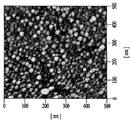
- FIG. 7A shows a two-dimensional image of a second conductive oxide layer by AFM.
- FIG. 7B shows a three-dimensional image of the second conductive oxide layer by AFM.
- FIG. 8A shows the operating voltages in case 3 and case 4.
- FIG. 8A shows the operating voltages in case 3 and case 4.
- FIG. 8B shows the light output of Case 3 and Case 4.
- FIG. 9B shows a scatter plot of the light output of Case 3 and Case 4.
- 10 is a table showing differences in operating voltages in cases 3 and 4 and differences in light output.
- FIG. 11 is a sectional view showing a light emitting device according to another embodiment.
- FIG. 12 illustrates a light emitting device package according to an embodiment.
- FIG. 13 illustrates a lighting apparatus according to an embodiment.
- FIG. 14 illustrates a display device according to an exemplary embodiment.
- each layer (region), region, pattern, or structure is “on” or “under” the substrate, each layer (film), region, pad, or pattern.
- “up” and “under” include both “directly” or “indirectly” formed through another layer. do.
- the criteria for up / down or down / down each layer will be described with reference to the drawings.
- Like reference numerals denote like elements throughout the description of the drawings.
- FIG. 1 is a sectional view of a light emitting device 100 according to an embodiment.
- the light emitting device 100 includes a substrate 110, a light emitting structure 120, a transparent conductive layer 130, a current blocking layer 140, a first electrode 152, and a second electrode 154. , And the reflective member 160.
- the substrate 110 is a substrate suitable for growing a nitride semiconductor single crystal, for example, any one of a sapphire substrate, a silicon (Si) substrate, a zinc oxide (ZnO) substrate, a nitride semiconductor substrate, or GaN, InGaN, AlGaN, AlInGaN. At least one may be a stacked template substrate.
- irregularities 111 may be formed on the surface of the substrate 110.
- the substrate 110 may be a patterned sapphire substrate (PSS) on which the unevenness 111 is formed, but is not limited thereto.
- PSS patterned sapphire substrate
- the light emitting structure 120 is disposed on the substrate 110 and generates light.
- the light emitting structure 120 may include a first conductive semiconductor layer 122, an active layer 124, and a second conductive semiconductor layer 126.
- the light emitting structure 120 may include a first conductive semiconductor layer 122 disposed on the substrate 110, a second conductive semiconductor layer 126 disposed on the first conductive semiconductor layer 122, and The active layer 124 may be disposed between the first conductive semiconductor layer 122 and the second conductive semiconductor layer 126.
- the first conductive semiconductor layer 122 may be disposed on the substrate 110, and may be a compound semiconductor such as Group 3-5, Group 2-6, or the like, and the first conductivity type dopant may be doped.
- the first conductive type semiconductor layer 122 may be a semiconductor having a composition formula of In x Al y Ga 1 -x- y N (0 ⁇ x ⁇ 1, 0 ⁇ y ⁇ 1, 0 ⁇ x + y ⁇ 1) Can be.
- the first conductivity type semiconductor layer 122 may include any one of InAlGaN, GaN, AlGaN, InGaN, AlN, InN, and the n-type dopant (eg, Si, Ge, Se, Te, etc.) may be doped.
- the n-type dopant eg, Si, Ge, Se, Te, etc.
- a layer or pattern using a compound semiconductor of Group 2 to Group 6 elements for example, a ZnO layer (not shown) and a buffer layer (not shown). At least one of the undoped semiconductor layer (not shown) may be formed.
- the buffer layer or the undoped semiconductor layer may be formed using a compound semiconductor of group III-V elements, and may have a single layer or a multilayer structure.
- the buffer layer reduces the difference in the lattice constant between the light emitting structure 120 and the substrate 110, and the undoped semiconductor layer may be formed of an undoped GaN-based semiconductor.
- the undoped GaN can be grown here as Unintentionally doped GaN (hereinafter referred to as "UID GaN”), in particular n-type UID GaN.
- UID GaN Unintentionally doped GaN
- N-vacancy may be deficient in N (sodium) even in a region where no n-type dopant is supplied, and as the N-vacancy increases, the concentration of surplus electrons increases, thereby producing a UID GaN process.
- unintended at UID GaN may exhibit electrical properties similar to those doped with n-type dopants.
- the active layer 124 is disposed on the first conductivity type semiconductor layer 122.
- the active layer 124 emits light by energy generated during the recombination of electrons and holes provided from the first conductive semiconductor layer 122 and the second conductive semiconductor layer 126. Can be generated.
- the active layer 124 may be a semiconductor compound such as Group 3-5, 2-6, or the like, and may be a compound semiconductor of Group 3-5, 2-6, and the like. It may have a quantum-wire structure, a quantum dot, or a quantum disk structure.
- the active layer 124 may have a composition formula of In x Al y Ga 1 -x- y N (0 ⁇ x ⁇ 1, 0 ⁇ y ⁇ 1, 0 ⁇ x + y ⁇ 1).
- the active layer 124 has a composition formula of In x Al y Ga 1 -xy N (0 ⁇ x ⁇ 1, 0 ⁇ y ⁇ 1, 0 ⁇ x + y ⁇ 1).
- the energy band gap of the well layer is lower than the energy band gap of the barrier layer.
- the well layer and the barrier layer may be alternately stacked at least once.
- the energy band gap of the well layer and the barrier layer may be constant in each section, but is not limited thereto.
- the composition of indium (In) and / or aluminum (Al) of the well layer may be constant, and the composition of indium (In) and / or aluminum (Al) of the barrier layer may be constant.
- the energy band gap of the well layer may include a section that gradually increases or decreases
- the energy band gap of the barrier layer may include a section that gradually increases or decreases
- the light emitting structure 120 may further include a superlattice layer disposed between the first conductive semiconductor layer 122 and the active layer 124 in order to alleviate the lattice constant.
- the second conductive semiconductor layer 126 may be disposed on the active layer 124, and may be a semiconductor compound such as Group 3-5, Group 2-6, or the like, and the second conductive dopant may be doped.
- the semiconductor having a composition formula of a second conductivity type semiconductor layer 126 is In x Al y Ga 1 -x- y N (0 ⁇ x ⁇ 1, 0 ⁇ y ⁇ 1, 0 ⁇ x + y ⁇ 1) Can be.
- the second conductivity-type semiconductor layer 126 may include any one of InAlGaN, GaN, AlGaN, InGaN, AlN, and InN, and a p-type dopant (eg, Mg, Zn, Ca, Sr, or Ba) may be doped.
- a p-type dopant eg, Mg, Zn, Ca, Sr, or Ba
- the light emitting structure 120 further includes an electron blocking layer disposed between the active layer 124 and the second conductivity type semiconductor layer 126 to prevent overflow of electrons and holes. You may.
- the first conductive semiconductor layer 122, the active layer 124, and the second conductive semiconductor layer 126 are sequentially stacked by etching or the like in the light emitting structure 120.
- the second conductive semiconductor layer 126 and one region of the active layer 124 are removed to expose one region of the first conductive semiconductor layer 122 positioned below.
- the light transmissive conductive layer 130 is disposed on the light emitting structure 120, for example, the second conductivity type semiconductor layer 126, thereby reducing the total reflection and improving light extraction efficiency.
- the current blocking layer 140 is disposed between the light emitting structure 120, for example, the second conductivity type semiconductor layer 126 and the transparent conductive layer 130.
- the current blocking layer 140 may at least partially overlap the second electrode 154 in the vertical direction.
- the vertical direction may be a direction from the first conductive semiconductor layer 122 to the second conductive semiconductor layer 126.
- the current blocking layer 140 may improve light emission efficiency of the light emitting device 100 by alleviating a phenomenon in which current is concentrated in a portion of the light emitting structure 120 positioned adjacent to the second electrode 154.
- the current blocking layer 140 may be an electrically insulating material, eg, ZnO, SiO 2 , SiON, Si 3 N 4 , Al 2 O 3, TiO 2 .
- the current blocking layer 140 may be a material forming a schottky contact with the second conductivity type semiconductor layer 126.
- the transparent conductive layer 130 may cover side and top surfaces of the current blocking layer 140.
- the first electrode 152 is electrically connected to the first conductive semiconductor layer 122, and the second electrode 154 is electrically connected to the light transmissive conductive layer 130.
- the first electrode 152 may be disposed on one region of the exposed first conductive semiconductor layer 122, and the second electrode 154 may be disposed on one region of the upper surface of the transparent conductive layer 130. have. Power may be provided to the light emitting structure 120 through the first electrode 152 and the second electrode 154.
- each of the first electrode 152 and the second electrode 154 may include an electrode pad for bonding wires.
- the first electrode 152 and the second electrode 154 may be formed of a metal material.
- the first electrode 152 and the second electrode 154 may be formed of a reflective electrode material having ohmic characteristics.
- the first electrode 152 and the second electrode 154 may include at least one of Mg, Zn, Al, Ag, W, Cu, Ni, Cr, Ti, Pd, Ir, Sn, Ru, Pt, Au, and Hf. It may include one.
- each of the first electrode 152 and the second electrode 154 is a contact layer made of Ti or Cr, a reflective layer made of Al or Ag, and a bonding made of Au, Sn, Ti, Cu, W, Ni, or Pt. It may be a multilayer structure comprising a layer.
- the reflective member 160 is disposed on the bottom surface of the substrate 110 and reflects light generated from the light emitting structure 120.
- the reflective member 160 may reflect light irradiated toward the substrate 110 from the active layer 124 of the light emitting structure 120.
- the reflective member 160 may be made of a reflective metal material such as Ag or Al, or may be made of a distributed Bragg reflector layer. In other embodiments, the reflective member 160 may be omitted.
- FIG. 2 illustrates an embodiment of the transparent conductive layer 130 shown in FIG. 1.
- the transparent conductive layer 130 may include a first conductive oxide layer 132 and a second conductive oxide layer 134 disposed on the first conductive oxide layer 132.
- the first conductive oxide layer 132 is disposed on the second conductive semiconductor layer 132.
- the first conductive oxide layer 132 may include at least one first metal element and oxygen.
- the first conductive oxide layer 132 may be a transparent conductive oxide, for example, indium tin oxide (ITO).
- the first conductive oxide layer 132 may include tin oxide (TO), indium zinc oxide (IZO), indium tin zinc oxide (ITZO), indium gallium zinc oxide (IGZO), and indium gallium tin oxide (IGTO). ), ATO (Antimony tin Oxide), or GZO (Gallium Zinc Oxide).
- TO tin oxide
- IZO indium zinc oxide
- ITZO indium tin zinc oxide
- IGZO indium gallium zinc oxide
- IGTO indium gallium tin oxide
- ATO Antimony tin Oxide
- GZO Gallium Zinc Oxide
- the current blocking layer 140 may be disposed between the second conductive semiconductor layer 126 and the first conductive oxide layer 132.
- the second conductive oxide layer 134 is formed or disposed on the surface 130a of the first conductive oxide layer 132, and gives Gibs free energy than the first metal element included in the first conductive oxide layer 132. It may be a transparent conductive oxide layer containing a low second metal element.
- the second conductive oxide layer 134 may include a compound of a transparent conductive oxide and a second metal element forming the first conductive oxide layer 132.
- the second conductive oxide layer 134 may include the same metal element, oxygen, and second metal element as the first metal element of the first conductive oxide layer 132.
- the second metal element may be bonded to dangling bonds of oxygen of the second conductive oxide layer 134.
- the second metal element may be Al, K, Zn, Cr, Mn, V, Si, Ti, U, Li, Mg, or Ca.
- the second metal element may be aluminum.
- 4A and 4B illustrate a method of forming the transparent conductive layer 130.
- a light emitting structure 120 is formed on a substrate 110 and a current is blocked on a region of an upper surface of the light emitting structure 120, for example, the second conductive semiconductor layer 126.
- Form layer 140 is formed on a substrate 110 and a current is blocked on a region of an upper surface of the light emitting structure 120, for example, the second conductive semiconductor layer 126.
- a transparent conductive oxide 132a is formed on the upper surface of the second conductive semiconductor layer 126 on which the current blocking layer 140 is formed.
- the transparent conductive oxide 132a may be the same as the material of the first conductive oxide layer 132 described above.
- the transparent conductive oxide 132a may be formed on a surface (eg, an upper surface) of the second conductive semiconductor layer 126.
- the thickness T1 of the transparent conductive oxide 132a may be 30 nm to 50 nm.
- the thickness T1 of the transparent conductive oxide 132a may be 40 nm to 45 nm.
- the thickness T1 of the transparent conductive oxide 132a may be 40 nm.
- a metal thin film 210 made of a second metal element material is formed on a surface (eg, an upper surface) of the transparent conductive oxide 132a.
- the thickness T2 of the metal thin film 210 may be 2 nm to 5 nm.
- the thickness T2 of the metal thin film 210 may be 3 nm to 4 nm.
- the thickness of the metal thin film 210 may be 3 nm.
- the annealing process of the resultant metal thin film 210 formed on the surface of the transparent conductive oxide 132a is performed in a nitrogen atmosphere to at least one of dangling bonds of oxygen of the transparent conductive oxide 132a.
- One and a second metal element (eg, Al) of the metal thin film 210 are bonded.
- the transparent conductive oxide layer 132a includes a first region S1 adjacent to an interface 205 between the transparent conductive oxide 132a and the metal thin film 210, and below the first region S1. It may include a second area (S2) located in.
- the dangling bonds of oxygen in the first region S1 of the transparent conductive oxide 132a and the second metal element (eg, Al) of the metal thin film 210 combine to form a second metal element (eg, A second conductive oxide layer 134, which is a conductive oxide layer bonded with Al), may be formed.
- a second metal element eg, A second conductive oxide layer 134, which is a conductive oxide layer bonded with Al
- a second metal element (eg, Al) of the metal thin film 210 having a thickness of 2 nm to 5 nm and dangling bonds of oxygen in the first region S1 of the transparent conductive oxide layer 132a are combined to form 8 nm.
- a second conductive oxide layer 134 having a thickness of ⁇ 12 nm may be formed.
- the thickness T3 of the second conductive oxide layer 134 may be 10 nm.
- the thickness T3 of the second conductive oxide layer 134 formed by the annealing process may be 16% to 40% of the thickness T1 of the transparent conductive oxide 132a.
- the thickness T3 of the second conductive oxide layer 134 may be 20% to 30% of the thickness T1 of the transparent conductive oxide 132a.
- the second conductive oxide layer 134 is formed by combining a second metal element (eg, Al) of the metal thin film 210 and dangling bonds of oxygen in the first region S1 of the transparent conductive oxide layer 132a. ) May comprise a compound of aluminum and oxygen (eg, Al 2 O 3 ).
- the second conductive oxide layer 134 may further include an Al-In-Sn-O compound of aluminum, indium, tin, and oxygen.
- the second conductive oxide layer 134 may further include an Al-In-O compound of aluminum, indium, and oxygen.
- the second conductive oxide layer 134 may further include an Al-Sn-O compound of aluminum, tin, and oxygen.
- the transparent conductive oxide layer 132a Since the second metal element (eg, Al) of the metal thin film 210 has lower Gibbs-free energy than the first metal element (eg, In, Sn) of the transparent conductive oxide layer 132a, the transparent conductive oxide layer 132a is used. It can be easily combined with dangling bonds of oxygen.
- the second metal element (eg, Al) of the metal thin film 210 has lower Gibbs-free energy than the first metal element (eg, In, Sn) of the transparent conductive oxide layer 132a. It can be easily combined with dangling bonds of oxygen.
- the second region S2 of the transparent conductive oxide 132a is a region that does not bond with the second metal element of the metal thin film 210 to be the first conductive oxide layer 132.
- the thickness T4 of the first conductive oxide layer 132 may be 18 nm to 42 nm. Also, for example, the thickness T4 of the first conductive oxide layer 132 may be 30 nm.
- the thickness T3 of the second conductive oxide layer 134 may be smaller than the thickness T4 of the first conductive oxide layer 132 (T3 ⁇ T4).
- the ratio T3: T4 of the thickness T3 of the second conductive oxide layer 134 and the thickness T4 of the first conductive oxide layer 132 may be 1: 1.5 to 1: 5.25.
- a ratio T3: T4 of the thickness T3 of the second conductive oxide layer 134 and the thickness T4 of the first conductive oxide layer 132 may be 1: 4.
- FIG. 5A illustrates an embodiment of a bond between a dangling bond of oxygen in the first conductive oxide layer 132 and a second metal element of the metal thin film 210.
- one of oxygen dangling bonds bonded to indium (In) of the first region S1 of the transparent conductive oxide layer 132a of FIG. 4A and the second metal of the metal thin film 210 may be used.
- an element eg, Al
- an Al-In-O compound may be formed.
- the surface of the transparent conductive oxide layer 132a has a plurality of dangling bonds of oxygen atoms, and traps electrons by the dangling bonds of oxygen atoms.
- the dangling bond of oxygen of the second metal element (eg, Al) of the metal thin film 210 and the first region S1 of the transparent conductive oxide layer 132a through annealing in a nitrogen atmosphere By combining them to form the oxygen compounds described in FIG. 4B, the number of dangling bonds of oxygen on the surface of the transparent conductive layer 130 can be reduced. For this reason, the embodiment may reduce the operating voltage of the light emitting device 100 by reducing the resistance (eg, specific resistance or sheet resistance) of the transparent conductive layer 130.
- FIG. 5B illustrates another embodiment of a bond between a dangling bond of oxygen of the first conductive oxide layer 132 and a second metal element of the metal thin film 210.
- the transparent conductive oxide layer 132a is polycrystalline, a large number of grain boundary defects exist, and due to such grain boundary defects, crystallinity is not good. It may act as a factor that absorbs or degrades light transmittance.
- the second metal element (eg, Al) of the metal thin film 210 is any one of dangling bonds of oxygen bonded with indium (In) of the first region S1 of the transparent conductive oxide layer 132a, and transparent. It may be coupled to the grain boundary of the conductive oxide 132a.
- the second metal element (eg, Al) of the metal thin film 210 is bonded to the grain boundary of the first region S1 of the transparent conductive oxide 132a, the crystallinity of the transparent conductive layer 130 may be improved. Light absorption by the grain boundary can be prevented, and light transmittance can be improved.
- FIG 3 illustrates a structure of a second conductive oxide layer 134 according to an embodiment.
- the second conductive oxide layer 134 may have a grain structure formed on the surface of the first conductive oxide layer 132.
- the grain structure of FIG. 3 may be grains shown in FIGS. 7A and 7B.
- the second conductive oxide layer 134 may have a structure including a plurality of grains (eg, 301 to 305).
- the plurality of grains 301 to 305 may be compounds in which oxygen of the transparent conductive oxide 132a and the second metal element of the metal thin film 210 are combined by an annealing process.
- the grain structure of FIG. 3 comprises (a) a compound of aluminum and oxygen (eg, Al 2 O 3 ), (b) a compound of aluminum, indium, tin, and oxygen (Al-In-Sn-O compound), ( c) an Al-In-O compound, and (d) an Al-Sn-O compound of aluminum, tin, and oxygen.
- a compound of aluminum and oxygen eg, Al 2 O 3
- Al-In-Sn-O compound aluminum, indium, tin, and oxygen
- Al-In-Sn-O compound Al-In-Sn-O compound
- Al-In-O compound Al-In-O compound
- each of the plurality of grains 301-305 may comprise (a) a compound of aluminum and oxygen (eg, Al 2 O 3 ), (b) a compound of aluminum, indium, tin, and oxygen (Al-In-Sn- O compound), (c) an Al-In-O compound, and (d) an Al, Sn, and Al-Sn-O compound.
- a compound of aluminum and oxygen eg, Al 2 O 3
- Al-In-Sn- O compound Al-In-Sn- O compound
- Al-In-O compound Al-In-O compound
- Al-Sn-O compound Al-In-O compound
- the second conductive oxide layer 134 may include a first region P1 in which the plurality of grains 301 to 305 are formed and a second region P2 positioned between the grains.
- the second region P2 may be a region in which the compounds of (a) to (d) are not formed.
- the second region P2 may be a partial region of the first conductive oxide layer 132 exposed by the plurality of grains 301 to 305.
- FIG. 7A shows a two-dimensional image of the second conductive oxide layer 134 by Atomic Force Microscope (AFM), and FIG. 7B shows a three-dimensional image of the second conductive oxide layer 134 by AFM.
- the size (width x length) of the images in FIGS. 7A and 7B is 0.5 ⁇ m ⁇ 0.5 ⁇ m.
- the second conductive oxide layer 134 may include a plurality of grains having protrusions on a surface thereof, and the heights of the plurality of grains may be 8 nm to 12 nm.
- the height of the plurality of grains may be 10 nm.
- the height may be a distance from the surface of the first conductive oxide layer 132 to the highest point of each of the plurality of grains.
- the thickness of the second conductive oxide layer 134 may be the same as the maximum value of the plurality of grains, but is not limited thereto. In another embodiment, the thickness of the second conductive oxide layer 134 may be an average value of the heights of the plurality of grains.
- the plurality of grains may comprise (a) compounds of aluminum and oxygen (eg Al 2 O 3 ), (b) aluminum, indium, tin, and oxygen (Al-In-Sn-O compounds), (c) aluminum, Second conductive oxide layer 134 because it includes at least one of indium, an Al-In-O compound, and (d) an aluminum, tin, and Al-Sn-O compound.
- the embodiment can reduce the operating voltage and improve the light transmittance.
- FIG. 6A shows the light transmittance of Case 1 (Case1) and Case 2 (Case2)
- FIG. 6B shows an enlarged view of the dotted line portion 12 of FIG. 6A.
- the dotted portion 12 in FIG. 6B shows the transmittance of light having a wavelength range of 400 nm to 500 nm.
- Case 1 is a case where only the transparent conductive oxide 132a is formed on the sapphire substrate.
- Case 2 is a case in which the transparent conductive layer 130 including the first conductive oxide layer 132 and the second conductive oxide layer 134 is formed on the sapphire substrate as described with reference to FIGS. 4A and 4B.
- g1 is a light transmittance with respect to the transparent conductive oxide 132a in case 1
- g2 is a light transmittance with respect to the transmissive conductive layer 130 in case 2.
- the second metal element of the second conductive oxide layer 134 is aluminum (Al)
- the transparent conductive oxide 132a is ITO.
- the light transmittance of g2 is increased by 1% compared to g1 for light having a wavelength range of 400 nm to 500 nm.
- FIG. 8A shows the operating voltages of Case 3 (Case3) and Case 4 (Case4)
- FIG. 8B shows the light output of Case 3 (Case3) and Case 4 (Case4).
- Case 3 represents the operating voltage of the light emitting device including the light transmissive conductive layer consisting of ITO only
- case 4 represents the operating voltage of the light emitting device according to the embodiment including the transmissive conductive layer 130.
- Case 3 (Case 3) and case 4 (Case 4) differ only in the structure of the light transmissive conductive layer, and the structure of the other light emitting device and the experimental conditions for measuring the operating voltage are the same.
- the operating voltage of Case 4 (Case4) is lower than the operating voltage of Case 3 (Case3).
- the light output of Case 4 (Case4) is light of Case 3 (Case3). It is higher than the output.
- FIG. 9A shows a scatter diagram of the operating voltages of Case 3 (Case3) and Case 4 (Case4)
- FIG. 9B shows a scatter diagram of the light outputs of Case 3 (Case3) and Case 4 (Case4).
- FIG. 10 is a table showing the difference ⁇ Vf between the operating voltage VF3 of Case 3 (Case3) and Case 4 (Case4), and the ratio ⁇ Po of light outputs of Case 3 (Case3) and Case 4 (Case4). .
- the wavelengths WD of the light emitting devices of Case 3 and Case 4 (Case 4) are the same, and the operating voltage VF 3 of Case 3 (Case 3) and Case 4 (Case 4) of FIG. 10, and the light output ( Po) may be an average value of experimental data values.
- the operating voltage of Case 4 (Case4) minus the operating voltage of Case 3 (Case3) is ⁇ 0.019 [V].
- the operating voltage of Case 4 (Case4) is lower than that of Case 3 (Case3).
- the light output of Case 4 may be 102.6% of the light output of Case 3 (Case3). In other words, the light output of Case 4 (Case4) is higher than that of Case 3.
- a metal thin film 210 made of a second metal element having a lower Gibbs-free energy than the first metal element included in the first conductive oxide layer 132 is formed on the surface of the first conductive oxide layer 132 and annealed in a nitrogen atmosphere.
- the second conductive oxide layer 134 which is a compound of the second metal element and the conductive oxide described above, may be formed by bonding the dangling bond of oxygen of the second metal element and the first conductive oxide layer 132 through a process. .
- the embodiment lowers the resistance of the transparent conductive layer 130 to lower the operating voltage and improves the light transmittance by improving the crystallinity of the transparent conductive layer 130. have.
- FIG. 11 is a sectional view of a light emitting device 200 according to another embodiment.
- the same reference numerals as in FIG. 1 denote the same components, and the description of the same components will be simplified or omitted.
- the light emitting device 200 may further include a transparent conductive layer 170 in the invention device 100 shown in FIG. 1.
- the transparent conductive layer 170 may be disposed between the first conductive semiconductor layer 126 and the first electrode 152.
- the transparent conductive layer 170 may include a first conductive oxide layer 172 and a second conductive oxide layer 174.
- the description of the first conductive oxide layer 132 described with reference to FIGS. 2 to 10 may be applied to the first conductive oxide layer 172 illustrated in FIG. 11, and the description of the second conductive oxide layer 134 is illustrated in FIG. It may be applied to the second conductive oxide layer 174 shown in 11.
- the embodiment 200 can lower the operating voltage and improve the light extraction efficiency.
- FIG. 12 illustrates a light emitting device package according to an embodiment.
- the light emitting device package may include a package body 510, a first metal layer 512, a second metal layer 514, a light emitting device 520, a first wire 522, a second wire 524, The reflection plate 530 and the resin layer 540 are included.
- the package body 510 has a structure in which a cavity is formed in one region.
- the side wall of the cavity may be formed to be inclined.
- the package body 510 may be formed of a substrate having good insulation or thermal conductivity, such as a silicon-based wafer level package, a silicon substrate, silicon carbide (SiC), aluminum nitride (AlN), or the like. It may have a structure in which a plurality of substrates are stacked. Embodiment is not limited to the material, structure, and shape of the body described above.
- the first metal layer 512 and the second metal layer 514 are disposed on the surface of the package body 510 to be electrically separated from each other in consideration of heat dissipation or mounting of a light emitting device.
- the first and second metal layers 512 and 514 may be used interchangeably with the terms first and second lead frames.
- the light emitting device 520 is electrically connected to the first metal layer 512 and the second metal layer 514 through the first wire 522 and the second wire 524.
- the first wire 522 electrically connects the second electrode 154 and the first metal layer 512 of the light emitting devices 100 and 200 illustrated in FIGS. 1 and 11, and the second wire 524 is formed of the first wire 524.
- the first electrode 152 and the second metal layer 514 may be electrically connected to each other.
- the reflective plate 530 is formed on the side wall of the cavity of the package body 510 to direct light emitted from the light emitting element 520 in a predetermined direction.
- the reflector plate 530 is made of a light reflective material, and may be, for example, a metal coating or a metal flake.
- the resin layer 540 surrounds the light emitting device 520 positioned in the cavity of the package body 510 to protect the light emitting device 520 from the external environment.
- the resin layer 540 is made of a colorless transparent polymer resin material such as epoxy or silicon.
- the resin layer 540 may include a phosphor to change the wavelength of light emitted from the light emitting device 520.
- a plurality of light emitting device packages according to the exemplary embodiment illustrated in FIG. 12 may be arranged on a substrate, and a light guide plate, a prism sheet, a diffusion sheet, and the like, which are optical members, may be disposed on an optical path of the light emitting device package.
- the light emitting device package, the substrate, and the optical member may function as a backlight unit.
- Another embodiment may be implemented as a display device, an indicator device, or a lighting system including the light emitting device or the light emitting device package described in the above embodiments, and for example, the lighting system may include a lamp or a street lamp.
- FIG. 13 illustrates a lighting apparatus according to an embodiment.
- the lighting apparatus may include a cover 1100, a light source module 1200, a heat sink 1400, a power supply 1600, an inner case 1700, and a socket 1800.
- the lighting apparatus according to the embodiment may further include any one or more of the member 1300 and the holder 1500.
- the cover 1100 may have a shape of a bulb or hemisphere, may be hollow, and may have a shape in which a portion thereof is opened.
- the cover 1100 may be optically coupled to the light source module 1200.
- the cover 1100 may diffuse, scatter, or excite light provided from the light source module 1200.
- the cover 1100 may be a kind of optical member.
- the cover 1100 may be combined with the heat sink 1400.
- the cover 1100 may have a coupling portion coupled to the heat sink 1400.
- the inner surface of the cover 1100 may be coated with a milky paint.
- the milky paint may include a diffuser to diffuse light.
- the surface roughness of the inner surface of the cover 1100 may be greater than the surface roughness of the outer surface of the cover 1100. This is for the light from the light source module 1200 to be sufficiently scattered and diffused to be emitted to the outside.
- the material of the cover 1100 may be glass, plastic, polypropylene (PP), polyethylene (PE), polycarbonate (PC), or the like.
- polycarbonate is excellent in light resistance, heat resistance, and strength.
- the cover 1100 may be transparent so that the light source module 1200 is visible from the outside, but is not limited thereto and may be opaque.
- the cover 1100 may be formed through blow molding.
- the light source module 1200 may be disposed on one surface of the heat sink 1400, and heat generated from the light source module 1200 may be conducted to the heat sink 1400.
- the light source module 1200 may include a light source unit 1210, a connection plate 1230, and a connector 1250.
- the light source unit 1210 may include the light emitting devices 100 and 200 according to the embodiment, or the light emitting device package illustrated in FIG. 12.
- the member 1300 may be disposed on an upper surface of the heat sink 1400 and has a plurality of light source units 1210 and a guide groove 1310 into which the connector 1250 is inserted.
- the guide groove 1310 may correspond to or be aligned with the board and the connector 1250 of the light source 1210.
- the surface of the member 1300 may be coated or coated with a light reflecting material.
- the surface of the member 1300 may be coated or coated with a white paint.
- the member 1300 may reflect light reflected from the inner surface of the cover 1100 back toward the light source module 1200 in the direction of the cover 1100. Therefore, it is possible to improve the light efficiency of the lighting apparatus according to the embodiment.
- the member 1300 may be made of an insulating material, for example.
- the connection plate 1230 of the light source module 1200 may include an electrically conductive material. Thus, electrical contact may be made between the heat sink 1400 and the connection plate 1230.
- the member 1300 may be made of an insulating material to block an electrical short between the connection plate 1230 and the heat sink 1400.
- the radiator 1400 may radiate heat by receiving heat from the light source module 1200 and heat from the power supply unit 1600.
- the holder 1500 blocks the accommodating groove 1719 of the insulating portion 1710 of the inner case 1700. Therefore, the power supply unit 1600 accommodated in the insulating unit 1710 of the inner case 1700 may be sealed.
- the holder 1500 may have a guide protrusion 1510, and the guide protrusion 1510 may have a hole through which the protrusion 1610 of the power supply 1600 passes.
- the power supply unit 1600 processes or converts an electrical signal provided from the outside to provide the light source module 1200.
- the power supply unit 1600 may be accommodated in the accommodating groove 1719 of the inner case 1700, and may be sealed in the inner case 1700 by the holder 1500.
- the power supply 1600 may include a protrusion 1610, a guide 1630, a base 1650, and an extension 1670.
- the guide part 1630 may have a shape protruding outward from one side of the base 1650.
- the guide part 1630 may be inserted into the holder 1500.
- a plurality of parts may be disposed on one surface of the base 1650.
- a plurality of components may include, for example, a DC converter for converting AC power provided from an external power source into a DC power source, a driving chip for controlling driving of the light source module 1200, and an ESD (ElectroStatic) to protect the light source module 1200. discharge) protection elements and the like, but is not limited thereto.
- the extension 1670 may have a shape protruding to the outside from the other side of the base 1650.
- the extension 1670 may be inserted into the connection 1750 of the inner case 1700, and may receive an electrical signal from the outside.
- the extension 1670 may be equal to or smaller in width than the connection 1750 of the inner case 1700.
- Each end of the "+ wire” and the “-wire” may be electrically connected to the extension 1670, and the other end of the "+ wire” and the "-wire” may be electrically connected to the socket 1800. .
- the inner case 1700 may include a molding unit together with a power supply unit 1600 therein.
- the molding part is a part in which the molding liquid is hardened, and allows the power supply 1600 to be fixed inside the inner case 1700.
- FIG. 14 illustrates a display device 800 according to an exemplary embodiment.
- the display device 800 includes a bottom cover 810, a reflector 820 disposed on the bottom cover 810, light emitting modules 830 and 835 that emit light, and a reflector 820.
- An optical sheet including a light guide plate 840 disposed in front of the light guide plate and guiding light emitted from the light emitting modules 830 and 835 to the front of the display device, and prism sheets 850 and 860 disposed in front of the light guide plate 840.
- a display panel 870 disposed in front of the optical sheet, an image signal output circuit 872 connected to the display panel 870 and supplying an image signal to the display panel 870, and disposed in front of the display panel 870.
- the color filter 880 may be included.
- the bottom cover 810, the reflector 820, the light emitting modules 830 and 835, the light guide plate 840, and the optical sheet may form a backlight unit.
- the light emitting module may include light emitting device packages 835 mounted on the substrate 830.
- the PCB 830 may be used.
- the light emitting device package 835 may be the embodiment shown in FIG. 12.
- the bottom cover 810 may receive components in the display device 800.
- the reflective plate 820 may be provided as a separate component as shown in the drawing, or may be provided in the form of a high reflective material on the rear surface of the light guide plate 840 or the front surface of the bottom cover 810. .
- the reflective plate 820 may use a material having a high reflectance and being extremely thin, and may use polyethylene terephthalate (PET).
- PET polyethylene terephthalate
- the light guide plate 830 may be formed of polymethyl methacrylate (PMMA), polycarbonate (PC), polyethylene (PE), or the like.
- the first prism sheet 850 may be formed of a translucent and elastic polymer material on one surface of the support film, and the polymer may have a prism layer in which a plurality of three-dimensional structures are repeatedly formed.
- the plurality of patterns may be provided in the stripe type and the valley repeatedly as shown.
- the direction of the floor and the valley of one surface of the support film in the second prism sheet 860 may be perpendicular to the direction of the floor and the valley of one surface of the support film in the first prism sheet 850. This is to evenly distribute the light transmitted from the light emitting module and the reflective sheet to the front surface of the display panel 1870.
- a diffusion sheet may be disposed between the light guide plate 840 and the first prism sheet 850.
- the diffusion sheet may be made of a polyester and polycarbonate-based material, and may maximize the light projection angle through refraction and scattering of light incident from the backlight unit.
- the diffusion sheet includes a support layer including a light diffusing agent, a first layer and a second layer formed on the light exit surface (the first prism sheet direction) and the light incident surface (the reflection sheet direction) and do not include the light diffusing agent. It may include.
- the diffusion sheet, the first prism sheet 850, and the second prism sheet 860 form an optical sheet, which optical sheet is made of another combination, for example, a micro lens array or a diffusion sheet and a micro lens array. Or a combination of one prism sheet and a micro lens array.
- a liquid crystal display panel may be disposed in the display panel 870.
- another type of display device that requires a light source may be provided.
- the embodiment can be used in a light emitting device, a light emitting device package, a lighting device, and a display device that can lower the operating voltage and improve light extraction efficiency.
Landscapes
- Led Devices (AREA)
Abstract
실시 예는 기판, 기판 상에 배치되는 제1 도전형 반도체층, 제1 도전형 반도체층 상에 배치되는 제2 도전형 반도체층, 및 제1 도전형 반도체층과 제2 도전형 반도체층 사이에 배치되는 활성층을 포함하는 발광 구조물, 및 제2 도전형 반도체층 상에 배치되는 투광성 전도층을 포함하며, 투광성 전도층은 제1 도전형 반도체층에 배치되고 적어도 하나의 제1 금속 원소, 및 산소를 포함하는 제1 전도성 산화물층 및 제1 전도성 산화물층 상에 배치되고 적어도 하나의 제1 금속 원소와 동일한 금속 원소, 제2 금속 원소, 및 산소의 화합물로 이루어진 제2 전도성 산화물층을 포함한다.
Description
실시 예는 발광 소자에 관한 것이다.
GaN 등의 Ⅲ-Ⅴ족 질화물 반도체는, 우수한 물리적, 화학적 특성으로 인해 발광 다이오드(LED), 레이저 다이오드(LD), 태양 전지 등의 반도체 광소자의 핵심 소재로 각광을 받고 있다.
질화물 반도체 발광 소자는 핸드폰의 백라이트(backlight)나 키패드, 전광판, 조명 장치 등 각종 제품의 광원으로 응용되고 있다. 특히, 디지털 제품이 진화함에 따라, 보다 큰 휘도와 높은 신뢰성을 갖는 질화물 반도체 광소자에 대한 요구가 증가하고 있다.
발광 다이오드는 사파어어 기판에 성장된 발광 구조물을 포함하는 구조를 가질 수 있다. 여기서 발광 구조물은 n형 반도체층, 활성층, 및 p형 반도체층을 포함할 수 있다. 활성층은 일반적으로 전자를 구속할 수 있는 다중 양자 우물 구조를 가질 수 있다.
실시 예는 동작 전압을 낮추고 광 추출 효율을 향상시킬 수 있는 발광 소자를 제공한다.
실시 예에 따른 발광 소자는 기판; 상기 기판 상에 배치되고, 제1 도전형 반도체층, 활성층, 및 제2 도전형 반도체층을 포함하는 발광 구조물; 및 상기 제2 도전형 반도체층 상에 배치되는 투광성 전도층을 포함하며, 상기 투광성 전도층은 상기 제1 도전형 반도체층에 배치되고, 적어도 하나의 제1 금속 원소, 및 산소를 포함하는 제1 전도성 산화물층; 및 상기 제1 전도성 산화물층 상에 배치되고, 상기 적어도 하나의 제1 금속 원소와 동일한 금속 원소, 제2 금속 원소, 및 산소의 화합물로 이루어진 제2 전도성 산화물층을 포함한다.
상기 제2 금속 원소의 깁스 프리 에너지는 상기 제1 금속 원소의 깁스 프리 에너지보다 작을 수 있다.
상기 제2 금속 원소는 상기 제2 전도성 산화물층의 산소의 댕글링 본드와 결합할 수 있다.
상기 적어도 하나의 제1 금속 원소는 인듐 및 주석이고, 상기 제2 금속 원소는 알루미늄일 수 있다.
상기 제2 전도성 산화물층은 알루미늄, 및 산소의 화합물; 알루미늄, 인듐, 주석, 및 산소의 화합물; 알루미늄, 인듐, 및 산소의 화합물; 및 알루미늄, 주석, 및 산소의 화합물 중 적어도 하나를 포함할 수 있다.
상기 제1 전도성 산화물층은 TO(Tin Oxide), IZO(Indium Zinc Oxide), ITZO(Indium Tin Zinc Oxide), IGZO(Indium Gallium Zinc Oxide), IGTO(Indium Gallium Tin Oxide), ATO(Antimony tin Oxide), 또는 GZO(Gallium Zinc Oxide) 중 어느 하나이고, 상기 제2 금속 원소는 Al, K, Zn, Cr, Mn,V, Si, Ti, U, Li, Mg, 또는 Ca일 수 있다.
상기 제2 전도성 산화물층의 두께는 상기 제1 전도성 산화물층의 두께보다 얇을 수 있다. 상기 제2 전도성 산화물층의 두께와 상기 제1 전도성 산화물층의 두께의 비는 1:1.5 ~ 1:5.25인 발광 소자.
다른 실시 예에 따른 발광 소자는 기판; 상기 기판 상에 배치되고, 제1 도전형 반도체층, 활성층, 및 제2 도전형 반도체층을 포함하는 발광 구조물; 및 상기 제2 도전형 반도체층 상에 배치되는 투광성 전도층을 포함하며, 상기 투광성 전도층은 상기 제1 도전형 반도체층에 배치되고, 제1 금속 원소를 포함하는 제1 전도성 산화물층; 및 상기 제1 전도성 산화물층 표면에 배치되고, 복수의 낱알들(grains)을 포함하는 제2 전도성 산화물들을 포함하며, 상기 복수의 낱알들(grains) 각각은 상기 제1 금속 원소와 동일한 금속 원소, 제2 금속 원소, 및 산소의 화합물로 이루어진다.
상기 제2 금속 원소의 깁스 프리 에너지는 상기 제1 금속 원소의 깁스 프리 에너지보다 작을 수 있다.
상기 제2 금속 원소는 상기 제2 전도성 산화물층의 산소의 댕글링 본드에 결합될 수 있다.
상기 낱알들 각각의 높이는 8nm ~ 12nm일 수 있다.
상기 제2 전도성 산화물층은 상기 낱알들이 형성되는 제1 영역; 및 상기 낱알들 사이에 위치하고, 상기 제1 전도성 산화물 표면의 일부를 노출하는 제2 영역을 포함할 수 있다.
상기 제1 금속 원소는 인듐 및 주석이고, 상기 제2 금속 원소는 알루미늄일 수 있다.
상기 제2 전도성 산화물층은 알루미늄, 및 산소의 화합물; 알루미늄, 인듐, 주석, 및 산소의 화합물; 알루미늄, 인듐, 및 산소의 화합물; 및 알루미늄, 주석, 및 산소의 화합물 중 적어도 하나를 포함할 수 있다.
상기 발광 소자는 상기 투광성 전도층 상에 배치되는 전극을 더 포함할 수 있다.
실시 예는 동작 전압을 낮추고 광 추출 효율을 향상시킬 수 있다.
도 1은 실시 예에 따른 발광 소자의 단면도를 나타낸다.
도 2는 도 1에 도시된 투광성 전도층의 일 실시 예를 나타낸다.
도 3은 제2 전도성 산화물층의 일 실시 예에 따른 구조를 나타낸다.
도 4a 및 도 4b는 투광성 전도층을 형성하는 방법을 나타낸다.
도 5a는 제1 전도성 산화물층의 산소의 댕글링 본드와 금속 박막의 제2 금속 원소 간의 결합의 일 실시 예를 나타낸다.
도 5b는 제1 전도성 산화물층의 산소의 댕글링 본드와 금속 박막의 제2 금속 원소 간의 결합의 다른 실시 예를 나타낸다.
도 6a는 경우 1과 경우 2의 광투과도를 나타낸다.
도 6b는 도 6a의 점선 부분의 확대도를 나타낸다.
도 7a는 AFM에 의한 제2 전도성 산화물층의 2차원 이미지를 나타낸다.
도 7b는 AFM에 의한 제2 전도성 산화물층의 3차원 이미지를 나타낸다.
도 8a는 경우 3과 경우 4의 동작 전압을 나타낸다.
도 8b는 경우 3과 경우 4의 광 출력을 나타낸다.
도 9a는 경우 3과 경우 4의 동작 전압의 산포도를 나타낸다.
도 9b는 경우 3과 경우 4의 광 출력의 산포도를 나타낸다.
도 10은 경우 3 및 경우 4의 동작 전압의 차이, 및 광 출력의 차이를 나타내는 표이다.
도 11은 다른 실시 예에 따른 발광 소자의 단면도를 나타낸다.
도 12는 실시 예에 따른 발광 소자 패키지를 나타낸다.
도 13은 실시 예에 따른 조명 장치를 나타낸다.
도 14는 실시 예에 따른 표시 장치를 나타낸다.
이하, 실시 예들은 첨부된 도면 및 실시 예들에 대한 설명을 통하여 명백하게 드러나게 될 것이다. 실시 예의 설명에 있어서, 각 층(막), 영역, 패턴 또는 구조물들이 기판, 각 층(막), 영역, 패드 또는 패턴들의 "상/위(on)"에 또는 "하/아래(under)"에 형성되는 것으로 기재되는 경우에 있어, "상/위(on)"와 "하/아래(under)"는 "직접(directly)" 또는 "다른 층을 개재하여 (indirectly)" 형성되는 것을 모두 포함한다. 또한 각 층의 상/위 또는 하/아래에 대한 기준은 도면을 기준으로 설명한다. 또한 동일한 참조번호는 도면의 설명을 통하여 동일한 요소를 나타낸다.
도 1은 실시 예에 따른 발광 소자(100)의 단면도를 나타낸다.
도 1을 참조하면, 발광 소자(100)는 기판(110), 발광 구조물(120), 투광성 전도층(130), 전류 차단층(140), 제1 전극(152), 제2 전극(154), 및 반사 부재(160)를 포함한다.
기판(110)은 질화물 반도체 단결정을 성장시키기에 적합한 기판으로서, 예컨대, 사파이어 기판, 실리콘(Si) 기판, 산화아연(ZnO) 기판, 질화물 반도체 기판 중 어느 하나, 또는 GaN, InGaN, AlGaN, AlInGaN 중에서 적어도 어느 하나가 적층된템플레이트(Template) 기판일 수 있다.
광 추출 효율을 높이기 위하여 기판(110) 표면에는 요철(111)이 형성될 수 있다. 예컨대. 기판(110)은 요철(111)이 형성된 사파이어 기판(patterned sapphire substrate: PSS)일 수 있으나, 이에 한정되는 것은 아니다.
발광 구조물(120)은 기판(110) 상에 배치되며, 빛을 발생시킨다.
발광 구조물(120)은 제1 도전형 반도체층(122), 활성층(124), 및 제2 도전형 반도체층(126)을 포함할 수 있다. 예컨대, 발광 구조물(120)은 기판(110) 상에 배치되는 제1 도전형 반도체층(122), 제1 도전형 반도체층(122) 상에 배치되는 제2 도전형 반도체층(126), 및 제1 도전형 반도체층(122)과 제2 도전형 반도체층(126) 사이에 배치되는 활성층(124)을 포함할 수 있다.
제1 도전형 반도체층(122)은 기판(110) 상에 배치되며, 3족-5족, 2족-6족 등의 화합물 반도체일 수 있고, 제1 도전형 도펀트가 도핑될 수 있다.
예컨대, 제1 도전형 반도체층(122)은 InxAlyGa1
-x-
yN(0≤x≤1, 0≤y≤1, 0≤x+y≤1)의 조성식을 가지는 반도체일 수 있다. 예컨대, 제1 도전형 반도체층(122)은 InAlGaN, GaN, AlGaN, InGaN, AlN, InN 중 어느 하나를 포함할 수 있으며, n형 도펀트(예: Si, Ge, Se, Te 등)가 도핑될 수 있다.
도 1에는 도시되지 않았지만, 기판(110)과 제1 도전형 반도체층(122) 사이에는 2족 내지 6족 원소의 화합물 반도체를 이용한 층 또는 패턴, 예컨대, ZnO층(미도시), 버퍼층(미도시), 언도프드 반도체층(미도시) 중 적어도 한 층이 형성될 수 있다.
버퍼층 또는 언도프드 반도체층은 3족-5족 원소의 화합물 반도체를 이용하여 형성될 수 있으며, 단일층 또는 다층 구조일 수 있다. 버퍼층은 발광 구조물(120)과 기판(110) 간의 격자 상수의 차이를 줄여주게 되며, 언도프드 반도체층은 도핑하지 않은 GaN계 반도체로 형성될 수 있다.
여기서 언도프드 GaN은 Unintentionally doped(의도하지 않은 언도프드) GaN(이하, "UID GaN"이라 칭한다), 특히 n-형의 UID GaN으로 성장될 수 있다. 예컨대, GaN의 성장 공정에서 n-형 도펀트를 공급하지 않는 영역에서도 N(나트륨)이 결핍된 N-vacancy가 발생할 수 있고, N-vacancy가 많아지면 잉여 전자의 농도가 커져서, UID GaN의 제조 공정에서 의도하지 않았더라고 UID GaN은 n-형 도펀트로 도핑된 것과 유사한 전기적인 특성을 나타낼 수도 있다.
활성층(124)은 제1 도전형 반도체층(122) 상에 배치된다.
활성층(124)은 제1 도전형 반도체층(122) 및 제2 도전형 반도체층(126)으로부터 제공되는 전자(electron)와 정공(hole)의 재결합(recombination) 과정에서 발생하는 에너지에 의해 광을 생성할 수 있다.
활성층(124)은 3족-5족, 2족-6족 등의 반도체 화합물, 예컨대, 3족-5족, 2족-6족의 화합물 반도체일 수 있으며, 단일 우물 구조, 다중 우물 구조, 양자 선(Quantum-Wire) 구조, 양자 점(Quantum Dot), 또는 양자 디스크(Quantum Disk) 구조를 가질 수 있다.
예컨대, 활성층(124)은 InxAlyGa1
-x-
yN(0≤x≤1, 0≤y≤1, 0≤x+y≤1)의 조성식을 가질 수 있다. 활성층(124)이 양자우물구조인 경우, 활성층(124)은 InxAlyGa1
-x-yN(0≤x≤1, 0≤y≤1, 0≤x+y≤1)의 조성식을 갖는 우물층(미도시) 및 InaAlbGa1
-a-bN(0≤a≤1, 0≤b≤1, 0≤a+b≤1)의 조성식을 갖는 장벽층(미도시)을 포함할 수 있다.
우물층의 에너지 밴드 갭은 장벽층의 에너지 밴드 갭보다 낮다. 우물층 및 장벽층은 적어도 1회 이상 교대로 적층될 수 있다.
우물층 및 장벽층의 에너지 밴드 갭은 각 구간에 일정할 수 있으나, 이에 한정되는 것은 아니다.
예컨대, 우물층의 인듐(In) 및/또는 알루미늄(Al)의 조성은 일정할 수 있고, 장벽층의 인듐(In) 및/또는 알루미늄(Al)의 조성은 일정할 수 있다.
또는 우물층의 에너지 밴드 갭은 점차 증가하거나 또는 점차 감소하는 구간을 포함할 수 있으며, 장벽층의 에너지 밴드 갭은 점차 증가하거나 또는 점차 감소하는 구간을 포함할 수 있다.
도 1에 도시되지 않았지만, 격자 상수의 완화를 위하여 발광 구조물(120)은 제1 도전형 반도체층(122)과 활성층(124) 사이에 배치되는 초격자층을 더 포함할 수도 있다.
제2 도전형 반도체층(126)은 활성층(124) 상에 배치되며, 3족-5족, 2족-6족 등의 반도체 화합물일 수 있고, 제2 도전형 도펀트가 도핑될 수 있다.
예컨대, 제2 도전형 반도체층(126)은 InxAlyGa1
-x-
yN(0≤x≤≤1, 0≤y≤1, 0≤x+y≤1)의 조성식을 가지는 반도체일 수 있다. 예컨대, 제2 도전형 반도체층(126)은 InAlGaN, GaN, AlGaN, InGaN, AlN, InN 중 어느 하나를 포함할 수 있으며, p형 도펀트(예: Mg, Zn, Ca,Sr, Ba)가 도핑될 수 있다.
도 1에는 도시되지 않았지만, 전자 및 정공의 오버플로우(overflow)를 방지하기 위하여 발광 구조물(120)은 활성층(124)과 제2 도전형 반도체층(126) 사이에 배치되는 전자 차단층을 더 포함할 수도 있다.
제1 전극(152)과 전기적 연결을 위하여 제1 도전형 반도체층(122), 활성층(124), 및 제2 도전형 반도체층(126)이 순차적으로 적층된 발광 구조물(120)에서 식각 등에 의하여 제2 도전형 반도체층(126), 및 활성층(124)의 일 영역을 제거하여 하부에 위치하는 제1 도전형 반도체층(122)의 일 영역이 노출된다.
투광성 전도층(130)은 발광 구조물(120), 예컨대, 제2 도전형 반도체층(126) 상에 배치되며, 전반사를 감소시키고, 투광성이 좋기 때문에 광 추출 효율을 향상시킬 수 있다.
전류 차단층(140)은 발광 구조물(120), 예컨대, 제2 도전형 반도체층(126)과 투광성 전도층(130) 사이에 배치된다.
전류 차단층(140)은 제2 전극(154)과 수직 방향으로 적어도 일부가 오버랩(overlap)될 수 있다. 여기서 수직 방향은 제1 도전형 반도체층(122)으로부터 제2 도전형 반도체층(126)으로 향하는 방향일 수 있다.
전류 차단층(140)은 제2 전극(154)에 인접하여 위치하는 발광 구조물(120)의 일부 영역으로 전류가 집중되는 현상을 완화하여 발광 소자(100)의 발광 효율을 향상시킬 수 있다.
전류 차단층(140)은 전기 절연 물질, 예컨대, ZnO, SiO2, SiON,Si3N4, Al2O3 , TiO2일 수 있다. 또는 전류 차단층(140)은 제2 도전형 반도체층(126)과 쇼트키 접촉(schottky contact)을 형성하는 물질일 수도 있다.
예컨대, 투광성 전도층(130)은 전류 차단층(140)의 측면 및 상면을 덮을 수 있다.
제1 전극(152)은 제1 도전형 반도체층(122)과 전기적으로 연결되고, 제2 전극(154)은 투광성 전도층(130)과 전기적으로 연결된다.
제1 전극(152)은 노출되는 제1 도전형 반도체층(122)의 일 영역 상에 배치될 수 있고, 제2 전극(154)은 투광성 전도층(130)의 상면의 일 영역에 배치될 수 있다. 제1 전극(152) 및 제2 전극(154)을 통하여 발광 구조물(120)에 전원이 제공될 수 있다.
예컨대, 제1 전극(152), 및 제2 전극(154) 각각은 와이어가 본딩되기 위한 전극 패드를 포함할 수 있다.
제1 전극(152) 및 제2 전극(154)은 금속 물질로 형성될 수 있다. 예컨대, 제1 전극(152) 및 제2 전극(154)은 오믹 특성을 갖는 반사 전극 재료로 형성될 수 있다. 예컨대, 제1 전극(152) 및 제2 전극(154)은 Mg, Zn, Al, Ag, W, Cu, Ni, Cr, Ti, Pd, Ir, Sn, Ru, Pt, Au, Hf 중 적어도 어느 하나를 포함할 수 있다.
예컨대, 제1 전극(152) 및 제2 전극(154) 각각은 Ti 또는 Cr로 이루어지는 접촉층, Al 또는 Ag로 이루어지는 반사층, 및 Au, Sn, Ti, Cu, W, Ni, 또는 Pt로 이루어진 본딩층을 포함하는 다층 구조일 수 있다.
반사 부재(160)는 기판(110) 하면에 배치되며, 발광 구조물(120)로부터 발생하는 빛을 반사시킨다. 반사 부재(160)는 발광 구조물(120)의 활성층(124)으로부터 기판(110) 방향으로 조사되는 빛을 반사시킬 수 있다.
반사 부재(160)는 Ag 또는 Al 등의 반사 금속 물질로 이루어지거나 또는 분산 브래그 반사층(Distributed Bragg Reflector layer)으로 이루어질 수 있다. 다른 실시 예에서 반사 부재(160)는 생략될 수 있다.
도 2는 도 1에 도시된 투광성 전도층(130)의 일 실시 예를 나타낸다.
도 2를 참조하면, 투광성 전도층(130)은 제1 전도성 산화물층(132), 및 제1 전도성 산화물층(132) 상에 배치되는 제2 전도성 산화물층(134)을 포함할 수 있다.
제1 전도성 산화물층(132)은 제2 도전형 반도체층(132) 상에 배치된다.
제1 전도성 산화물층(132)은 적어도 하나의 제1 금속 원소, 및 산소를 포함할 수 있다. 제1 전도성 산화물층(132)은 투명 전도성 산화물, 예컨대, ITO(Indium Tin Oxide)일 수 있다.
예컨대, 다른 실시 예에서 제1 전도성 산화물층(132)은 TO(Tin Oxide), IZO(Indium Zinc Oxide), ITZO(Indium Tin Zinc Oxide), IGZO(Indium Gallium Zinc Oxide), IGTO(Indium Gallium Tin Oxide), ATO(Antimony tin Oxide), 또는 GZO(Gallium Zinc Oxide) 중 어느 하나로 이루어질 수도 있다.
예컨대, 전류 차단층(140)은 제2 도전형 반도체층(126)과 제1 전도성 산화물층(132) 사이에 배치될 수 있다.
제2 전도성 산화물층(134)은 제1 전도성 산화물층(132) 표면(130a)에 형성 또는 배치되며, 제1 전도성 산화물층(132)에 포함된 제1 금속 원소보다 깁스 프리 에너지(Gibbs free energy)가 낮은 제2 금속 원소를 포함하는 투명 전도성 산화물층일 수 있다.
제2 전도성 산화물층(134)은 제1 전도성 산화물층(132)을 이루는 투명 전도성 산화물과 제2 금속 원소의 화합물을 포함할 수 있다.
예컨대, 제2 전도성 산화물층(134)은 제1 전도성 산화물층(132)의 제1 금속 원소와 동일한 금속 원소, 산소, 및 제2 금속 원소를 포함할 수 있다. 제2 금속 원소는 제2 전도성 산화물층(134)의 산소의 댕글링 본드(dangling bond)와 결합할 수 있다.
예컨대, 제2 금속 원소는 Al, K, Zn, Cr, Mn, V, Si, Ti, U, Li, Mg, 또는 Ca일 수 있다. 예컨대, 제2 금속 원소는 알루미늄일 수 있다.
도 4a 및 도 4b는 투광성 전도층(130)을 형성하는 방법을 나타낸다.
도 1 및 도 4a를 참조하면, 기판(110) 상에 발광 구조물(120)을 형성하고, 발광 구조물(120), 예컨대, 제2 도전형 반도체층(126)의 상면의 일 영역 상에 전류 차단층(140)을 형성한다.
그리고 전류 차단층(140)이 형성된 제2 도전형 반도체층(126)의 상면에 투명 전도성 산화물(132a)을 형성한다. 예컨대, 투명 전도성 산화물(132a)은 상술한 제1 전도성 산화물층(132)의 물질과 동일할 수 있다.
예컨대, 제2 도전형 반도체층(126)의 표면(예컨대, 상면)에 투명 전도성 산화물(132a)을 형성할 수 있다. 예컨대, 형성되는 투명 전도성 산화물(132a)의 두께(T1)는 30nm ~ 50nm일 수 있다. 또는 예컨대, 투명 전도성 산화물(132a)의 두께(T1)는 40nm ~ 45nm일 수 있다. 또는 예컨대, 투명 전도성 산화물(132a)의 두께(T1)는 40nm일 수 있다.
다음으로 투명 전도성 산화물(132a) 표면(예컨대, 상면)에 제2 금속 원소 물질로 이루어진 금속 박막(210)을 형성한다. 예컨대, 금속 박막(210)의 두께(T2)는 2nm ~ 5nm일 수 있다. 또는 예컨대, 금속 박막(210)의 두께(T2)는 3nm ~ 4nm일 수 있다. 또는 예컨대, 금속 박막(210)의 두께는 3nm일 수 있다.
다음으로 투명 전도성 산화물(132a)의 표면에 금속 박막(210)이 형성된 결과물을 질소 분위기에서 어닐링(Annealing) 공정을 수행하여 투명 전도성 산화물(132a)의 산소의 댕글링 본드들(dangling bonds) 중 적어도 하나와 금속 박막(210)의 제2 금속 원소(예컨대, Al)를 결합시킨다.
도 4b를 참조하면, 투명 전도성 산화물층(132a)은 투명 전도성 산화물(132a)과 금속 박막(210) 사이의 경계면(205)에 인접하는 제1 영역(S1), 및 제1 영역(S1) 아래에 위치하는 제2 영역(S2)을 포함할 수 있다.
어닐링 공정에 의하여 투명 전도성 산화물(132a)의 제1 영역(S1)의 산소의 댕글링 본드들과 금속 박막(210)의 제2 금속 원소(예컨대, Al)가 결합하여 제2 금속 원소(예컨대, Al)가 결합된 전도성 산화물층인 제2 전도성 산화물층(134)이 형성될 수 있다.
예컨대, 어닐링 공정에 의하여 2nm ~ 5nm의 금속 박막(210)의 제2 금속 원소(예컨대, Al)와 투명 전도성 산화물층(132a)의 제1 영역(S1)의 산소의 댕글링 본드들이 결합하여 8nm ~ 12nm 두께의 제2 전도성 산화물층(134)이 형성될 수 있다. 예컨대, 제2 전도성 산화물층(134)의 두께(T3)는 10nm일 수 있다.
어닐링 공정에 의하여 형성되는 제2 전도성 산화물층(134)의 두께(T3)는 투명 전도성 산화물(132a)의 두께(T1)의 16% ~ 40%일 수 있다. 또는 예컨대, 제2 전도성 산화물층(134)의 두께(T3)는 투명 전도성 산화물(132a)의 두께(T1)의 20% ~ 30%일 수도 있다
예컨대, 금속 박막(210)의 제2 금속 원소(예컨대, Al)와 투명 전도성 산화물층(132a)의 제1 영역(S1)의 산소의 댕글링 본드들의 결합에 의하여, 제2 전도성 산화물층(134)은 알루미늄 및 산소의 화합물(예컨대, Al2O3)을 포함할 수 있다.
또한 제2 전도성 산화물층(134)은 알루미늄, 인듐, 주석, 및 산소의 화합물(Al-In-Sn-O compound)을 더 포함할 수 있다.
또는 제2 전도성 산화물층(134)은 알루미늄, 인듐, 산소의 화합물(Al-In-O compound)을 더 포함할 수 있다.
또는 제2 전도성 산화물층(134)은 알루미늄, 주석, 및 산소의 화합물(Al-Sn-O compound)을 더 포함할 수 있다.
금속 박막(210)의 제2 금속 원소(예컨대, Al)가 투명 전도성 산화물층(132a)의 제1 금속 원소(예컨대, In, Sn)보다 깁스 프리 에너지가 낮기 때문에, 투명 전도성 산화물층(132a)의 산소의 댕글링 본드와 용이하게 결합할 수 있다.
투명 전도성 산화물(132a)의 제2 영역(S2)은 금속 박막(210)의 제2 금속 원소와 결합하지 않는 영역으로 제1 전도성 산화물층(132)이 될 수 있다.
예컨대, 제1 전도성 산화물층(132)의 두께(T4)는 18nm ~ 42nm일 수 있다. 또한 예컨대, 제1 전도성 산화물층(132)의 두께(T4)는 30nm일 수 있다.
제2 전도성 산화물층(134)의 두께(T3)는 제1 전도성 산화물층(132)의 두께(T4)보다 작을 수 있다(T3<T4).
예컨대, 제2 전도성 산화물층(134)의 두께(T3)와 제1 전도성 산화물층(132)의 두께(T4)의 비(T3:T4)는 1:1.5 ~ 1:5.25일 수 있다. 예컨대, 제2 전도성 산화물층(134)의 두께(T3)와 제1 전도성 산화물층(132)의 두께(T4)의 비(T3:T4)는 1:4일 수 있다.
도 5a는 제1 전도성 산화물층(132)의 산소의 댕글링 본드와 금속 박막(210)의 제2 금속 원소 간의 결합의 일 실시 예를 나타낸다.
도 5a를 참조하면, 도 4a의 투명 전도성 산화물층(132a)의 제1 영역(S1)의 인듐(In)과 결합하는 산소의 댕글링 본드들 중 어느 하나와 금속 박막(210)의 제2 금속 원소(예컨대, Al)와 결합하여 알루미늄, 인듐, 산소의 화합물(Al-In-O compound)을 형성할 수 있다.
투명 전도성 산화물층(132a)의 표면은 산소 원자의 댕글링 본드들이 다수 존재하며, 이러한 산소 원자의 댕글링 본드들에 의하여 전자의 트랩이 발생한다.
실시 예는 상술한 바와 같이, 질소 분위기에서 어닐링을 통하여 금속 박막(210)의 제2 금속 원소(예컨대, Al)와 투명 전도성 산화물층(132a)의 제1 영역(S1)의 산소의 댕글링 본드들을 결합시켜, 도 4b에서 설명한 산소 화합물들을 형성하기 때문에, 투광성 전도층(130) 표면의 산소의 댕글링 본드들의 수를 감소시킬 수 있다. 이로 인하여 실시 예는 투광성 전도층(130)의 저항(예컨대, 비저항(specific resistance) 또는 면저항)을 감소시켜 발광 소자(100)의 동작 전압을 낮출 수 있다.
도 5b 제1 전도성 산화물층(132)의 산소의 댕글링 본드와 금속 박막(210)의 제2 금속 원소 간의 결합의 다른 실시 예를 나타낸다.
도 5b를 참조하면, 투명 전도성 산화물층(132a)은 다결정이기 때문에 많은 수의 그레인 바운더리(grain boundary) 결함이 존재하며, 이러한 그레인 바운더리 결함에 의하여 결정성이 좋지 않고, 이러한 그레인 바운더리 결함은 광을 흡수하거나 또는 광 투과도를 떨어뜨리는 요인으로 작용할 수 있다.
금속 박막(210)의 제2 금속 원소(예컨대, Al)는 투명 전도성 산화물층(132a)의 제1 영역(S1)의 인듐(In)과 결합하는 산소의 댕글링 본드들 중 어느 하나, 및 투명 전도성 산화물(132a)의 그레인 바운더리에 결합될 수 있다.
금속 박막(210)의 제2 금속 원소(예컨대, Al)는 투명 전도성 산화물(132a)의 제1 영역(S1)의 그레인 바운더리에 결합되기 때문에, 투광성 전도층(130)의 결정성을 향상시킬 수 있고, 그레인 바운더리에 의한 광 흡수가 방지될 수 있고, 광 투과도가 향상될 수 있다.
도 3은 제2 전도성 산화물층(134)의 일 실시 예에 따른 구조를 나타낸다.
도 3을 참조하면, 제2 전도성 산화물층(134)은 제1 전도성 산화물층(132)의 표면에 형성되는 낱알(grain) 구조를 가질 수 있다. 예컨대, 도 3의 낱알 구조는 도 7a 및 도 7b에 도시된 낱알들(grains)일 수 있다.
제2 전도성 산화물층(134)은 복수의 낱알들(grains, 예컨대, 301 내지 305)을 포함하는 구조를 가질 수 있다.
복수의 낱알들(301 내지 305)은 어닐링 공정에 의하여 투명 전도성 산화물(132a)의 산소와 금속 박막(210)의 제2 금속 원소가 결합된 화합물들일 수 있다.
예컨대, 도 3의 낱알 구조는 (a) 알루미늄 및 산소의 화합물(예컨대, Al2O3), (b) 알루미늄, 인듐, 주석, 및 산소의 화합물(Al-In-Sn-O compound), (c) 알루미늄,인듐, 산소의 화합물(Al-In-O compound), 및 (d) 알루미늄,주석, 및 산소의 화합물(Al-Sn-O compound) 중 적어도 하나를 포함할 수 있다.
예컨대, 복수의 낱알들(301 내지 305) 각각은 (a) 알루미늄 및 산소의 화합물(예컨대, Al2O3), (b) 알루미늄, 인듐, 주석, 및 산소의 화합물(Al-In-Sn-O compound), (c) 알루미늄,인듐, 산소의 화합물(Al-In-O compound), 및 (d) 알루미늄,주석, 및 산소의 화합물(Al-Sn-O compound) 중 어느 하나를 포함할 수 있다.
상술한 (a) 내지 (d)의 화합물들이 불규칙적으로 분포 또는 배치되어 존재하기 때문에, 그 형상 및 크기가 일정하거나 서로 동일하지 않을 수 있다. 예컨대, 제2 전도성 산화물층(134)은 복수의 낱알들(301 내지 305)이 형성되는 제1 영역(P1) 및 낱알들 사이에 위치하는 제2 영역(P2)을 포함할 수 있다.
제2 영역(P2)은 상술한 (a) 내지 (d)의 화합물이 형성되지 않는 영역일 수 있다. 예컨대, 제2 영역(P2)은 복수의 낱알들(301 내지 305)에 의하여 노출되는 제1 전도성 산화물층(132)의 일부 영역일 수 있다.
도 7a는 AFM(Atomic Force Microscope)에 의한 제2 전도성 산화물층(134)의 2차원 이미지를 나타내고, 도 7b는 AFM에 의한 제2 전도성 산화물층(134)의 3차원 이미지를 나타낸다. 도 7a 및 도 7b의 이미지의 크기(가로 길이× 세로의 길이)는 0.5㎛ × 0.5㎛이다.
도 7a 및 도 7b를 참조하면, 제2 전도성 산화물층(134)은 표면에 돌기 형상의 복수의 낱알들을 포함할 수 있으며, 복수의 낱알들의 높이는 8nm ~ 12nm일 수 있다. 예컨대, 복수의 낱알들의 높이는 10nm일 수 있다. 여기서 높이는 제1 전도성 산화물층(132)의 표면으로부터 복수의 낱알들 각각의 최고점까지의 거리일 수 있다. 예컨대, 제2 전도성 산화물층(134)의 두께는 복수의 낱알들의 높이들 중 최고값과 동일할 수 있으나, 이에 한정되는 것은 아니며, 다른 실시 예에서는 복수의 낱알들의 높이들의 평균값일 수도 있다.
복수의 낱알들은 (a)알루미늄 및 산소의 화합물(예컨대, Al2O3), (b) 알루미늄, 인듐, 주석, 및 산소의 화합물(Al-In-Sn-O compound), (c) 알루미늄,인듐, 산소의 화합물(Al-In-O compound), 및 (d) 알루미늄,주석, 및 산소의 화합물(Al-Sn-O compound) 중 적어도 하나를 포함하기 때문에, 제2 전도성 산화물층(134)의 저항(예컨대, 비저항 또는 면저항)이 감소될 수 있고, 제2 전도성 산화물층(134)의 그레인 바운더리(grain boundary) 결함의 수를 줄임으로써 투광성 전도층(130)의 결정성을 향상시킬 수 있다, 이로 인하여 실시 예는 동작 전압을 감소시킬 수 있고, 광투과도를 향상시킬 수 있다.
도 6a는 경우 1(Case1)과 경우 2(Case2)의 광투과도를 나타내고, 도 6b는 도 6a의 점선 부분(12)의 확대도를 나타낸다. 도 6b의 점선 부분(12)은 400nm ~ 500nm의 파장 범위를 갖는 광의 투과도를 나타낸다.
경우 1(Case1)은 사파이어 기판에 투명 전도성 산화물(132a)만을 형성한 경우이다. 경우 2(Case2)는 도 4a 및 도 4b에서 설명한 바와 같이 사파이어 기판에 제1 전도성 산화물층(132) 및 제2 전도성 산화물층(134)을 포함하는 투광성 전도층(130)을 형성한 경우이다.
g1은 경우 1의 투명 전도성 산화물(132a)에 관한 광투과도이고, g2는 경우 2의 투광성 전도층(130)에 관한 광투과도이다. g2에서 제2 전도성 산화물층(134)의 제2 금속 원소는 알루미늄(Al)이고, 투명 전도성 산화물(132a)은 ITO이다.
도 6a 및 도 6b를 참조하면, 400nm ~ 500nm의 파장 범위를 갖는 광에 대하여 g2의 광투과도가 g1에 비하여 1%만큼 상승한다.
도 8a는 경우 3(Case3)과 경우 4(Case4)의 동작 전압을 나타내고, 도 8b는 경우 3(Case3)과 경우 4(Case4)의 광 출력을 나타낸다.
경우 3(Case3)은 ITO로만 이루어진 투광성 전도층을 포함하는 발광 소자의 동작 전압을 내고, 경우 4(Case4)는 투광성 전도층(130)을 포함하는 실시 예에 따른 발광 소자의 동작 전압을 나타낸다. 경우 3(Case3) 및 경우 4(Case4)는 투광성 전도층의 구조만 다를 뿐이고, 그 밖의 발광 소자의 구조 및 동작 전압 측정을 위한 실험 조건은 양자가 동일하다.
도 8a를 참조하면, 경우 4(Case4)의 동작 전압이 경우 3(Case3)의 동작 전압에 비하여 낮아진다, 또한 도 8b를 참조하면, 경우 4(Case4)의 광 출력이 경우 3(Case3)의 광 출력에 비하여 높아진다.
도 9a는 경우 3(Case3)과 경우 4(Case4)의 동작 전압의 산포도를 나타내고, 도 9b는 경우 3(Case3)과 경우 4(Case4)의 광 출력의 산포도를 나타낸다.
도 9a를 참조하면, 경우 4(Case4)의 발광 소자들의 동작 전압들의 대부분이 경우 3(Case3)의 발광 소자들의 동작 전압에 비하여 낮은 값을 갖도록 분포된다. 또한 도 9b를 참조하면, 경우 4(Case4)의 발광 소자들의 광 출력들의 대부분이 경우 3(Case3)의 발광 소자들의 광 출력들보다 높은 값을 갖도록 분포된다.
도 10은 경우 3(Case3) 및 경우 4(Case4)의 동작 전압(VF3)의 차이(ΔVf), 및 경우 3(Case3) 및 경우 4(Case4)의 광 출력의 비율(ΔPo)을 나타내는 표이다.
도 10에서 경우 3 및 경우 4(Case4) 각각의 발광 소자의 파장(WD)은 서로 동일하며, 도 10의 경우 3(Case3) 및 경우 4(Case4)의 동작 전압(VF3), 및 광 출력(Po)은 실험 데이터 값들의 평균값일 수 있다.
도 10을 참조하면, 경우 4(Case4)의 동작 전압에서 경우 3(Case3)의 동작 전압을 뺀 값은 -0.019[V]이다. 즉 경우 4(Case4)의 동작 전압이 경우 3(Case3)의 동작 전압보다 낮다.
경우 4(Case4)의 광 출력은 경우 3(Case3)의 광 출력의 102.6%일 수 있다. 즉 경우 4(Case4)의 광 출력이 경우 3의 광 출력보다 높다.
제1 전도성 산화물층(132)에 포함된 제1 금속 원소보다 깁스 프리 에너지가 낮은 제2 금속 원소로 이루어진 금속 박막(210)을 제1 전도성 산화물층(132) 표면에 형성하고, 질소 분위기의 어닐링 공정을 통하여 제2 금속 원소와 제1 전도성 산화물층(132)의 산소의 댕글링 본드를 결합시켜 상술한 제2 금속 원소와 전도성 산화물의 화합물인 제2 전도성 산화물층(134)이 형성될 수 있다.
이렇게 형성된 제2 전도성 산화물층(134)에 의하여 실시 예는 투광성 전도층(130)의 저항을 낮추어 동작 전압을 낮춤과 동시에, 투광성 전도층(130)의 결정성을 향상시켜 광 투과도를 향상시킬 수 있다.
도 11은 다른 실시 예에 따른 발광 소자(200)의 단면도를 나타낸다. 도 1과 동일한 도면 부호는 동일한 구성을 나타내며, 동일한 구성에 대해서는 설명을 간략하게 하거나 생략한다.
도 11을 참조하면, 발광 소자(200)는 도 1에 도시된 발명 소자(100)에 투광성 전도층(170)을 더 포함할 수 있다.
투광성 전도층(170)은 제1 도전형 반도체층(126)과 제1 전극(152) 사이에 배치될 수 있다.
투광성 전도층(170)은 제1 전도성 산화물층(172) 및 제2 전도성 산화물층(174)을 포함할 수 있다.
도 2 내지 도 10에서 설명한 제1 전도성 산화물층(132)에 대한 설명은 도 11에 도시된 제1 전도성 산화물층(172)에 적용될 수 있고, 제2 전도성 산화물층(134)에 대한 설명은 도 11에 도시된 제2 전도성 산화물층(174)에 적용될 수 있다.
투광성 전도층(170)에 의하여 실시 예(200)는 동작 전압을 낮출 수 있고, 광 추출 효율을 향상시킬 수 있다.
도 12는 실시 예에 따른 발광 소자 패키지를 나타낸다.
도 12를 참조하면, 발광 소자 패키지는 패키지 몸체(510), 제1 금속층(512), 제2 금속층(514), 발광 소자(520), 제1 와이어(522), 제2 와이어(524), 반사판(530) 및 수지층(540)을 포함한다.
패키지 몸체(510)는 일측 영역에 캐비티(cavity)가 형성된 구조이다.
캐비티의 측벽은 경사지게 형성될 수 있다. 패키지 몸체(510)는 실리콘 기반의 웨이퍼 레벨 패키지(wafer level package), 실리콘 기판, 실리콘 카바이드(SiC), 질화알루미늄(aluminum nitride, AlN) 등과 같이 절연성 또는 열전도도가 좋은 기판으로 형성될 수 있으며, 복수 개의 기판이 적층되는 구조일 수 있다. 실시 예는 상술한 몸체의 재질, 구조, 및 형상으로 한정되지 않는다.
제1 금속층(512) 및 제2 금속층(514)은 열 배출이나 발광 소자의 장착을 고려하여 서로 전기적으로 분리되도록 패키지 몸체(510)의 표면에 배치된다. 제1 및 제2 금속층들(512,514)은 제1 및 제2 리드 프레임들이라는 용어로 대체하여 사용될 수 있다.
발광 소자(520)는 제1 와이어(522) 및 제2 와이어(524)를 통하여 제1 금속층(512) 및 제2 금속층(514)과 전기적으로 연결된다.
예컨대, 제1 와이어(522)는 도 1 및 도 11에 도시된 발광 소자(100,200)의 제2 전극(154)과 제1 금속층(512)을 전기적으로 연결하고, 제2 와이어(524)는 제1 전극(152)과 제2 금속층(514)을 전기적으로 연결할 수 있다.
반사판(530)은 발광 소자(520)에서 방출된 빛을 소정의 방향으로 지향하도록 패키지 몸체(510)의 캐비티 측벽에 형성된다. 반사판(530)은 광반사 물질로 이루어지며, 예컨대, 금속 코팅이거나 금속 박편일 수 있다.
수지층(540)은 패키지 몸체(510)의 캐비티 내에 위치하는 발광 소자(520)를 포위하여 발광 소자(520)를 외부 환경으로부터 보호한다. 수지층(540)은 에폭시 또는 실리콘과 같은 무색 투명한 고분자 수지 재질로 이루어진다. 수지층(540)은 발광 소자(520)에서 방출된 광의 파장을 변화시킬 수 있도록 형광체가 포함될 수 있다.
도 12에 도시된 실시 예에 따른 발광 소자 패키지는 복수 개가 기판 상에 어레이되고, 발광 소자 패키지의 광 경로 상에 광학 부재인 도광판, 프리즘 시트, 확산 시트 등이 배치될 수 있다. 이러한 발광 소자 패키지, 기판, 광학 부재는 백라이트 유닛으로 기능할 수 있다.
또 다른 실시 예는 상술한 실시 예들에 기재된 발광 소자 또는 발광 소자 패키지를 포함하는 표시 장치, 지시 장치, 조명 시스템으로 구현될 수 있으며, 예를 들어, 조명 시스템은 램프, 가로등을 포함할 수 있다.
도 13은 실시 예에 따른 조명 장치를 나타낸다.
도 13을 참조하면, 조명 장치는 커버(1100), 광원 모듈(1200), 방열체(1400), 전원 제공부(1600), 내부 케이스(1700), 및 소켓(1800)을 포함할 수 있다. 또한, 실시 예에 따른 조명 장치는 부재(1300)와 홀더(1500) 중 어느 하나 이상을 더 포함할 수 있다.
커버(1100)는 벌브(bulb) 또는 반구의 형상일 수 있으며, 속이 비어 있고, 일 부분이 개구된 형상일 수 있다. 커버(1100)는 광원 모듈(1200)과 광학적으로 결합될 수 있다. 예를 들어, 커버(1100)는 광원 모듈(1200)로부터 제공되는 빛을 확산, 산란 또는 여기시킬 수 있다. 커버(1100)는 일종의 광학 부재일 수 있다. 커버(1100)는 방열체(1400)와 결합될 수 있다. 커버(1100)는 방열체(1400)와 결합하는 결합부를 가질 수 있다.
커버(1100)의 내면에는 유백색 도료가 코팅될 수 있다. 유백색의 도료는 빛을 확산시키는 확산재를 포함할 수 있다. 커버(1100)의 내면의 표면 거칠기는 커버(1100)의 외면의 표면 거칠기보다 크게 형성될 수 있다. 이는 광원 모듈(1200)로부터의 빛이 충분히 산란 및 확산되어 외부로 방출시키기 위함이다.
커버(1100)의 재질은 유리(glass), 플라스틱, 폴리프로필렌(PP), 폴리에틸렌(PE), 폴리카보네이트(PC) 등일 수 있다. 여기서, 폴리카보네이트는 내광성, 내열성, 강도가 뛰어나다. 커버(1100)는 외부에서 광원 모듈(1200)이 보이도록 투명할 수 있으나, 이에 한정되는 것은 아니고 불투명할 수 있다. 커버(1100)는 블로우(blow) 성형을 통해 형성될 수 있다.
광원 모듈(1200)은 방열체(1400)의 일 면에 배치될 수 있으며, 광원 모듈(1200)로부터 발생한 열은 방열체(1400)로 전도될 수 있다. 광원 모듈(1200)은 광원부(1210), 연결 플레이트(1230), 및 커넥터(1250)를 포함할 수 있다. 광원부(1210)는 실시 예에 따른 발광 소자(100,200), 또는 도 12에 도시된 발광 소자 패키지를 포함할 수 있다.
부재(1300)는 방열체(1400)의 상면 위에 배치될 수 있고, 복수의 광원부(1210)들과 커넥터(1250)가 삽입되는 가이드홈(1310)을 갖는다. 가이드홈(1310)은 광원부(1210)의 기판 및 커넥터(1250)와 대응 또는 정렬될 수 있다.
부재(1300)의 표면은 광 반사 물질로 도포 또는 코팅된 것일 수 있다.
예를 들면, 부재(1300)의 표면은 백색의 도료로 도포 또는 코팅된 것일 수 있다. 이러한 부재(1300)는 커버(1100)의 내면에 반사되어 광원 모듈(1200)을 향하여 되돌아오는 빛을 다시 커버(1100) 방향으로 반사할 수 있다. 따라서, 실시 예에 따른 조명 장치의 광 효율을 향상시킬 수 있다.
부재(1300)는 예로서 절연 물질로 이루어질 수 있다. 광원 모듈(1200)의 연결 플레이트(1230)는 전기 전도성의 물질을 포함할 수 있다. 따라서, 방열체(1400)와 연결 플레이트(1230) 사이에 전기적인 접촉이 이루어질 수 있다. 부재(1300)는 절연 물질로 구성되어 연결 플레이트(1230)와 방열체(1400)의 전기적 단락을 차단할 수 있다. 방열체(1400)는 광원 모듈(1200)로부터의 열과 전원 제공부(1600)로부터의 열을 전달받아 방열할 수 있다.
홀더(1500)는 내부 케이스(1700)의 절연부(1710)의 수납홈(1719)을 막는다. 따라서, 내부 케이스(1700)의 절연부(1710)에 수납되는 전원 제공부(1600)는 밀폐될 수 있다. 홀더(1500)는 가이드 돌출부(1510)를 가질 수 있으며, 가이드 돌출부(1510)는 전원 제공부(1600)의 돌출부(1610)가 관통하는 홀을 가질 수 있다.
전원 제공부(1600)는 외부로부터 제공받은 전기적 신호를 처리 또는 변환하여 광원 모듈(1200)로 제공한다. 전원 제공부(1600)는 내부 케이스(1700)의 수납홈(1719)에 수납될 수 있고, 홀더(1500)에 의해 내부 케이스(1700)의 내부에 밀폐될 수 있다. 전원 제공부(1600)는 돌출부(1610), 가이드부(1630), 베이스(1650), 연장부(1670)를 포함할 수 있다.
가이드부(1630)는 베이스(1650)의 일 측에서 외부로 돌출된 형상을 가질 수 있다. 가이드부(1630)는 홀더(1500)에 삽입될 수 있다. 베이스(1650)의 일 면 위에는 다수의 부품이 배치될 수 있다. 다수의 부품은 예를 들어, 외부 전원으로부터 제공되는 교류 전원을 직류 전원으로 변환하는 직류변환장치, 광원 모듈(1200)의 구동을 제어하는 구동칩, 광원 모듈(1200)을 보호하기 위한 ESD(ElectroStatic discharge) 보호 소자 등을 포함할 수 있으나 이에 대해 한정하지는 않는다.
연장부(1670)는 베이스(1650)의 다른 일 측에서 외부로 돌출된 형상을 가질 수 있다. 연장부(1670)는 내부 케이스(1700)의 연결부(1750) 내부에 삽입될 수 있고, 외부로부터의 전기적 신호를 제공받을 수 있다. 예컨대, 연장부(1670)는 내부 케이스(1700)의 연결부(1750)와 폭이 같거나 작을 수 있다. 연장부(1670)에는 "+ 전선"과 "- 전선"의 각 일 단이 전기적으로 연결될 수 있고, "+ 전선"과 "- 전선"의 다른 일 단은 소켓(1800)에 전기적으로 연결될 수 있다.
내부 케이스(1700)는 내부에 전원 제공부(1600)와 함께 몰딩부를 포함할 수 있다. 몰딩부는 몰딩 액체가 굳어진 부분으로서, 전원 제공부(1600)가 내부 케이스(1700) 내부에 고정될 수 있도록 한다.
도 14는 실시 예에 따른 표시 장치(800)를 나타낸다.
도 14를 참조하면, 표시 장치(800)는 바텀 커버(810)와, 바텀 커버(810) 상에 배치되는 반사판(820)과, 광을 방출하는 발광 모듈(830, 835)과, 반사판(820)의 전방에 배치되며 발광 모듈(830,835)에서 발산되는 빛을 표시 장치 전방으로 안내하는 도광판(840)과, 도광판(840)의 전방에 배치되는 프리즘 시트들(850,860)을 포함하는 광학 시트와, 광학 시트 전방에 배치되는 디스플레이 패널(870)과, 디스플레이 패널(870)과 연결되고 디스플레이 패널(870)에 화상 신호를 공급하는 화상 신호 출력 회로(872)와, 디스플레이 패널(870)의 전방에 배치되는 컬러 필터(880)를 포함할 수 있다. 여기서 바텀 커버(810), 반사판(820), 발광 모듈(830,835), 도광판(840), 및 광학 시트는 백라이트 유닛(Backlight Unit)을 이룰 수 있다.
발광 모듈은 기판(830) 상에 실장되는 발광 소자 패키지들(835)을 포함할 수 있다. 여기서, 기판(830)은 PCB 등이 사용될 수 있다. 발광 소자 패키지(835)는 도 12에 도시된 실시 예일 수 있다.
바텀 커버(810)는 표시 장치(800) 내의 구성 요소들을 수납할 수 있다. 그리고, 반사판(820)은 본 도면처럼 별도의 구성요소로 마련될 수도 있으며, 도광판(840)의 후면이나, 바텀 커버(810)의 전면에 반사도가 높은 물질로 코팅되는 형태로 마련되는 것도 가능하다.
여기서, 반사판(820)은 반사율이 높고 초박형으로 사용 가능한 소재를 사용할 수 있고, 폴리에틸렌 테레프탈레이트(PolyEthylene Terephtalate; PET)를 사용할 수 있다.
그리고, 도광판(830)은 폴리메틸메타크릴레이트(PolyMethylMethAcrylate; PMMA), 폴리카보네이트(PolyCarbonate; PC), 또는 폴리에틸렌(PolyEthylene; PE) 등으로 형성될 수 있다.
그리고, 제1 프리즘 시트(850)는 지지 필름의 일면에, 투광성이면서 탄성을 갖는 중합체 재료로 형성될 수 있으며, 중합체는 복수 개의 입체구조가 반복적으로 형성된 프리즘층을 가질 수 있다. 여기서, 복수 개의 패턴은 도시된 바와 같이 마루와 골이 반복적으로 스트라이프 타입으로 구비될 수 있다.
그리고, 제2 프리즘 시트(860)에서 지지 필름 일면의 마루와 골의 방향은, 제1 프리즘 시트(850) 내의 지지필름 일면의 마루와 골의 방향과 수직할 수 있다. 이는 발광 모듈과 반사 시트로부터 전달된 빛을 디스플레이 패널(1870)의 전면으로 고르게 분산하기 위함이다.
그리고, 도시되지는 않았으나, 도광판(840)과 제1 프리즘 시트(850) 사이에 확산 시트가 배치될 수 있다. 확산 시트는 폴리에스터와 폴리카보네이트 계열의 재료로 이루어질 수 있으며, 백라이트 유닛으로부터 입사된 빛을 굴절과 산란을 통하여 광 투사각을 최대로 넓힐 수 있다. 그리고, 확산 시트는 광확산제를 포함하는 지지층과, 광출사면(제1 프리즘 시트 방향)과 광입사면(반사시트 방향)에 형성되며 광확산제를 포함하지 않는 제1 레이어와 제2 레이어를 포함할 수 있다.
실시 예에서 확산 시트, 제1 프리즘시트(850), 및 제2 프리즘시트(860)가 광학 시트를 이루는데, 광학 시트는 다른 조합 예를 들어, 마이크로 렌즈 어레이로 이루어지거나 확산 시트와 마이크로 렌즈 어레이의 조합 또는 하나의 프리즘 시트와 마이크로 렌즈 어레이의 조합 등으로 이루어질 수 있다.
디스플레이 패널(870)은 액정 표시 패널(Liquid crystal display)가 배치될 수 있는데, 액정 표시 패널(860) 외에 광원을 필요로 하는 다른 종류의 표시 장치가 구비될 수 있다.
이상에서 실시 예들에 설명된 특징, 구조, 효과 등은 본 발명의 적어도 하나의 실시 예에 포함되며, 반드시 하나의 실시 예에만 한정되는 것은 아니다. 나아가, 각 실시 예에서 예시된 특징, 구조, 효과 등은 실시 예들이 속하는 분야의 통상의 지식을 가지는 자에 의해 다른 실시 예들에 대해서도 조합 또는 변형되어 실시 가능하다. 따라서 이러한 조합과 변형에 관계된 내용들은 본 발명의 범위에 포함되는 것으로 해석되어야 할 것이다.
실시 예는 동작 전압을 낮추고 광 추출 효율을 향상시킬 수 있는 발광 소자, 발광 소자 패키지, 조명 장치, 및 표시 장치에 사용될 수 있다.
Claims (10)
- 기판;상기 기판 상에 배치되는 제1 도전형 반도체층, 상기 제1 도전형 반도체층 상에 배치되는 제2 도전형 반도체층, 및 상기 제1 도전형 반도체층과 상기 제2 도전형 반도체층 사이에 배치되는 활성층을 포함하는 발광 구조물; 및상기 제2 도전형 반도체층 상에 배치되는 투광성 전도층을 포함하며,상기 투광성 전도층은,상기 제1 도전형 반도체층에 배치되고, 적어도 하나의 제1 금속 원소, 및 산소를 포함하는 제1 전도성 산화물층; 및상기 제1 전도성 산화물층 상에 배치되고, 상기 적어도 하나의 제1 금속 원소와 동일한 금속 원소, 제2 금속 원소, 및 산소의 화합물로 이루어진 제2 전도성 산화물층을 포함하는 발광 소자.
- 제1항에 있어서,상기 제2 금속 원소의 깁스 프리 에너지는 상기 제1 금속 원소의 깁스 프리 에너지보다 작은 발광 소자.
- 제1항에 있어서,상기 제2 금속 원소는 상기 제2 전도성 산화물층의 산소의 댕글링 본드와 결합하는 발광 소자.
- 제1항에 있어서,상기 적어도 하나의 제1 금속 원소는 인듐 및 주석이고,상기 제2 금속 원소는 알루미늄인 발광 소자.
- 제4항에 있어서, 상기 제2 전도성 산화물층은,알루미늄, 및 산소의 화합물;알루미늄, 인듐, 주석, 및 산소의 화합물;알루미늄, 인듐, 및 산소의 화합물; 및알루미늄, 주석, 및 산소의 화합물 중 적어도 하나를 포함하는 발광 소자.
- 제1항에 있어서,상기 제2 전도성 산화물층의 두께는 상기 제1 전도성 산화물층의 두께보다 얇은 발광 소자.
- 제1항에 있어서,상기 제2 전도성 산화물층은 상기 제1 전도성 산화물층 표면에 배치되는 복수의 낱알들(grains)을 포함하고,상기 복수의 낱알들(grains) 각각은,상기 제1 금속 원소와 동일한 금속 원소, 제2 금속 원소, 및 산소의 화합물로 이루어진 발광 소자.
- 제7항에 있어서,상기 낱알들 각각의 높이는 8nm ~ 12nm인 발광 소자.
- 제7항에 있어서, 상기 제2 전도성 산화물층은,상기 낱알들이 형성되는 제1 영역; 및상기 낱알들 사이에 위치하고, 상기 제1 전도성 산화물 표면의 일부를 노출하는 제2 영역을 포함하는 발광 소자.
- 제7항에 있어서, 상기 복수의 낱알들은,알루미늄, 및 산소의 화합물;알루미늄, 인듐, 주석, 및 산소의 화합물;알루미늄, 인듐, 및 산소의 화합물; 및알루미늄, 주석, 및 산소의 화합물 중 적어도 하나를 포함하는 발광 소자.
Priority Applications (1)
| Application Number | Priority Date | Filing Date | Title |
|---|---|---|---|
| US16/300,412 US10847678B2 (en) | 2016-05-09 | 2017-05-04 | Light emitting device that includes a light-transmissive conductive layer |
Applications Claiming Priority (2)
| Application Number | Priority Date | Filing Date | Title |
|---|---|---|---|
| KR1020160056223A KR102476036B1 (ko) | 2016-05-09 | 2016-05-09 | 발광 소자 |
| KR10-2016-0056223 | 2016-05-09 |
Publications (1)
| Publication Number | Publication Date |
|---|---|
| WO2017196022A1 true WO2017196022A1 (ko) | 2017-11-16 |
Family
ID=60266557
Family Applications (1)
| Application Number | Title | Priority Date | Filing Date |
|---|---|---|---|
| PCT/KR2017/004719 Ceased WO2017196022A1 (ko) | 2016-05-09 | 2017-05-04 | 발광 소자 |
Country Status (3)
| Country | Link |
|---|---|
| US (1) | US10847678B2 (ko) |
| KR (1) | KR102476036B1 (ko) |
| WO (1) | WO2017196022A1 (ko) |
Cited By (1)
| Publication number | Priority date | Publication date | Assignee | Title |
|---|---|---|---|---|
| CN111952422A (zh) * | 2019-05-16 | 2020-11-17 | 晶元光电股份有限公司 | 半导体元件 |
Families Citing this family (2)
| Publication number | Priority date | Publication date | Assignee | Title |
|---|---|---|---|---|
| CN114600239A (zh) | 2019-10-28 | 2022-06-07 | 首尔伟傲世有限公司 | 显示用发光元件及具有其的led显示装置 |
| US11817435B2 (en) | 2019-10-28 | 2023-11-14 | Seoul Viosys Co., Ltd. | Light emitting device for display and LED display apparatus having the same |
Citations (5)
| Publication number | Priority date | Publication date | Assignee | Title |
|---|---|---|---|---|
| KR100632668B1 (ko) * | 2003-08-22 | 2006-10-11 | 엘지이노텍 주식회사 | 발광소자의 투명전극 및 그 제조방법 |
| KR20140141003A (ko) * | 2013-05-31 | 2014-12-10 | 서울바이오시스 주식회사 | 투명 전극 구조체를 갖는 발광 다이오드 및 그것을 제조하는 방법 |
| WO2015037182A1 (ja) * | 2013-09-10 | 2015-03-19 | ロック技研工業株式会社 | 透明導電性基材及び透明導電性基材の製造方法 |
| JP2015082655A (ja) * | 2013-10-24 | 2015-04-27 | 隆達電子股▲ふん▼有限公司 | 発光ダイオード構造 |
| KR20150126475A (ko) * | 2014-05-02 | 2015-11-12 | 순천대학교 산학협력단 | 다중 적층 구조의 투명 전극을 갖는 자외선 발광소자 및 그 제조방법 |
Family Cites Families (26)
| Publication number | Priority date | Publication date | Assignee | Title |
|---|---|---|---|---|
| CN101872822B (zh) | 2002-11-16 | 2013-12-18 | Lg伊诺特有限公司 | 光器件及其制造方法 |
| KR101034055B1 (ko) * | 2003-07-18 | 2011-05-12 | 엘지이노텍 주식회사 | 발광 다이오드 및 그 제조방법 |
| JP4507594B2 (ja) | 2003-12-26 | 2010-07-21 | 日亜化学工業株式会社 | 半導体発光素子 |
| US9524869B2 (en) * | 2004-03-11 | 2016-12-20 | Epistar Corporation | Nitride-based semiconductor light-emitting device |
| TWM261838U (en) * | 2004-09-16 | 2005-04-11 | Super Nova Optoelectronics Cor | Structure for GaN based LED with high light extraction efficiency |
| KR101393353B1 (ko) * | 2007-10-29 | 2014-05-13 | 서울바이오시스 주식회사 | 발광다이오드 |
| US8633501B2 (en) * | 2008-08-12 | 2014-01-21 | Epistar Corporation | Light-emitting device having a patterned surface |
| JP5191866B2 (ja) * | 2008-11-12 | 2013-05-08 | スタンレー電気株式会社 | 半導体発光素子の製造方法及び半導体発光素子 |
| JP2011009502A (ja) * | 2009-06-26 | 2011-01-13 | Showa Denko Kk | 発光素子、その製造方法、ランプ、電子機器及び機械装置 |
| KR101798231B1 (ko) * | 2010-07-05 | 2017-11-15 | 엘지이노텍 주식회사 | 발광 소자 |
| JP4960511B1 (ja) * | 2011-01-26 | 2012-06-27 | 株式会社東芝 | 半導体発光素子及びその製造方法 |
| KR20130007368A (ko) * | 2011-07-01 | 2013-01-18 | 엘지디스플레이 주식회사 | 발광다이오드 칩 및 그의 제조방법과, 발광다이오드 칩을 포함하는 액정표시장치 |
| JP6079628B2 (ja) * | 2011-07-26 | 2017-02-15 | 日亜化学工業株式会社 | 窒化物半導体発光素子 |
| US8912028B2 (en) * | 2011-08-17 | 2014-12-16 | Lg Display Co., Ltd. | Semiconductor light emitting device and method for manufacturing the same |
| KR20130035658A (ko) * | 2011-09-30 | 2013-04-09 | 서울옵토디바이스주식회사 | 발광 다이오드 소자용 기판 제조 방법 |
| US9490409B2 (en) * | 2011-10-24 | 2016-11-08 | Formosa Epitaxy Incorporation | Light emmiting diode chip |
| JP5888133B2 (ja) * | 2012-06-08 | 2016-03-16 | 豊田合成株式会社 | 半導体発光素子、発光装置 |
| KR102495290B1 (ko) * | 2012-12-28 | 2023-02-06 | 가부시키가이샤 한도오따이 에네루기 켄큐쇼 | 반도체 장치 |
| JP2015185548A (ja) | 2014-03-20 | 2015-10-22 | 豊田合成株式会社 | 半導体発光素子とその製造方法および発光装置 |
| US9755104B2 (en) * | 2014-05-09 | 2017-09-05 | Epistar Corporation | Method of manufacturing optoelectronic element having rough surface |
| KR102244427B1 (ko) * | 2014-06-02 | 2021-04-27 | 엘지이노텍 주식회사 | 조명 장치 |
| US9306126B2 (en) * | 2014-07-14 | 2016-04-05 | Intermolecular, Inc. | Oxides with thin metallic layers as transparent ohmic contacts for p-type and n-type gallium nitride |
| JP6269362B2 (ja) * | 2014-07-15 | 2018-01-31 | 豊田合成株式会社 | Iii族窒化物半導体発光素子とその製造方法 |
| US9548420B2 (en) * | 2015-04-20 | 2017-01-17 | Epistar Corporation | Light-emitting device and manufacturing method thereof |
| CN209729940U (zh) * | 2015-05-13 | 2019-12-03 | 首尔伟傲世有限公司 | 发光元件 |
| US20170069791A1 (en) * | 2015-09-08 | 2017-03-09 | Epistar Corporation | Light-emitting device and method of manufacturing thereof |
-
2016
- 2016-05-09 KR KR1020160056223A patent/KR102476036B1/ko active Active
-
2017
- 2017-05-04 WO PCT/KR2017/004719 patent/WO2017196022A1/ko not_active Ceased
- 2017-05-04 US US16/300,412 patent/US10847678B2/en not_active Expired - Fee Related
Patent Citations (5)
| Publication number | Priority date | Publication date | Assignee | Title |
|---|---|---|---|---|
| KR100632668B1 (ko) * | 2003-08-22 | 2006-10-11 | 엘지이노텍 주식회사 | 발광소자의 투명전극 및 그 제조방법 |
| KR20140141003A (ko) * | 2013-05-31 | 2014-12-10 | 서울바이오시스 주식회사 | 투명 전극 구조체를 갖는 발광 다이오드 및 그것을 제조하는 방법 |
| WO2015037182A1 (ja) * | 2013-09-10 | 2015-03-19 | ロック技研工業株式会社 | 透明導電性基材及び透明導電性基材の製造方法 |
| JP2015082655A (ja) * | 2013-10-24 | 2015-04-27 | 隆達電子股▲ふん▼有限公司 | 発光ダイオード構造 |
| KR20150126475A (ko) * | 2014-05-02 | 2015-11-12 | 순천대학교 산학협력단 | 다중 적층 구조의 투명 전극을 갖는 자외선 발광소자 및 그 제조방법 |
Cited By (2)
| Publication number | Priority date | Publication date | Assignee | Title |
|---|---|---|---|---|
| CN111952422A (zh) * | 2019-05-16 | 2020-11-17 | 晶元光电股份有限公司 | 半导体元件 |
| CN111952422B (zh) * | 2019-05-16 | 2025-05-16 | 晶元光电股份有限公司 | 半导体元件及半导体元件的封装结构 |
Also Published As
| Publication number | Publication date |
|---|---|
| KR20170126167A (ko) | 2017-11-17 |
| KR102476036B1 (ko) | 2022-12-12 |
| US20190165210A1 (en) | 2019-05-30 |
| US10847678B2 (en) | 2020-11-24 |
Similar Documents
| Publication | Publication Date | Title |
|---|---|---|
| WO2016089052A1 (ko) | 발광 모듈 | |
| WO2017069372A1 (en) | Light emitting diode chip having distributed bragg reflector | |
| WO2017119661A1 (ko) | 반도체 소자 | |
| WO2017030396A1 (ko) | 발광 소자, 이 소자를 포함하는 발광 소자 패키지 및 이 패키지를 포함하는 발광 장치 | |
| WO2015083932A1 (ko) | 발광 소자 및 이를 구비한 조명 장치 | |
| WO2013162337A1 (en) | Light emitting device and light emitting device package | |
| WO2017222341A1 (ko) | 반도체 소자 및 이를 포함하는 반도체 소자 패키지 | |
| WO2013183901A1 (ko) | 발광소자, 발광소자 패키지 및 라이트 유닛 | |
| WO2013183888A1 (ko) | 발광소자 | |
| WO2017074035A1 (ko) | 발광소자 패키지, 및 이를 포함하는 조명시스템 | |
| WO2015156588A1 (ko) | 발광소자 및 조명시스템 | |
| WO2018117699A1 (ko) | 반도체 소자 | |
| WO2014181996A1 (ko) | 발광 소자 | |
| WO2017135763A1 (ko) | 발광소자 및 이를 포함하는 발광소자 패키지 | |
| WO2015020358A1 (ko) | 발광소자 | |
| WO2015156504A1 (ko) | 발광소자 및 이를 구비하는 조명 시스템 | |
| WO2015111814A1 (ko) | 발광소자, 발광소자 패키지, 라이트 유닛 | |
| WO2014058224A1 (ko) | 발광소자 | |
| WO2017010851A1 (ko) | 발광 소자 패키지 | |
| WO2014046527A1 (ko) | 발광소자 | |
| WO2016209015A1 (ko) | 자외선 발광소자, 발광소자 패키지 및 조명장치 | |
| WO2016117905A1 (ko) | 광원 모듈 및 조명 장치 | |
| WO2013172606A1 (ko) | 발광소자, 발광소자 페키지 및 라이트 유닛 | |
| WO2019103556A1 (ko) | 반도체 소자 | |
| WO2013183878A1 (ko) | 발광소자, 발광소자 패키지 및 라이트 유닛 |
Legal Events
| Date | Code | Title | Description |
|---|---|---|---|
| NENP | Non-entry into the national phase |
Ref country code: DE |
|
| 121 | Ep: the epo has been informed by wipo that ep was designated in this application |
Ref document number: 17796322 Country of ref document: EP Kind code of ref document: A1 |
|
| 122 | Ep: pct application non-entry in european phase |
Ref document number: 17796322 Country of ref document: EP Kind code of ref document: A1 |