WO2017195892A1 - 光モジュール - Google Patents
光モジュール Download PDFInfo
- Publication number
- WO2017195892A1 WO2017195892A1 PCT/JP2017/018054 JP2017018054W WO2017195892A1 WO 2017195892 A1 WO2017195892 A1 WO 2017195892A1 JP 2017018054 W JP2017018054 W JP 2017018054W WO 2017195892 A1 WO2017195892 A1 WO 2017195892A1
- Authority
- WO
- WIPO (PCT)
- Prior art keywords
- photonics
- optical
- lightwave circuit
- optical waveguide
- optical fiber
- Prior art date
- Legal status (The legal status is an assumption and is not a legal conclusion. Google has not performed a legal analysis and makes no representation as to the accuracy of the status listed.)
- Ceased
Links
Images





Classifications
-
- G—PHYSICS
- G02—OPTICS
- G02B—OPTICAL ELEMENTS, SYSTEMS OR APPARATUS
- G02B6/00—Light guides; Structural details of arrangements comprising light guides and other optical elements, e.g. couplings
- G02B6/10—Light guides; Structural details of arrangements comprising light guides and other optical elements, e.g. couplings of the optical waveguide type
- G02B6/12—Light guides; Structural details of arrangements comprising light guides and other optical elements, e.g. couplings of the optical waveguide type of the integrated circuit kind
- G02B6/122—Basic optical elements, e.g. light-guiding paths
- G02B6/1228—Tapered waveguides, e.g. integrated spot-size transformers
-
- G—PHYSICS
- G02—OPTICS
- G02B—OPTICAL ELEMENTS, SYSTEMS OR APPARATUS
- G02B6/00—Light guides; Structural details of arrangements comprising light guides and other optical elements, e.g. couplings
- G02B6/24—Coupling light guides
- G02B6/42—Coupling light guides with opto-electronic elements
- G02B6/4201—Packages, e.g. shape, construction, internal or external details
- G02B6/4202—Packages, e.g. shape, construction, internal or external details for coupling an active element with fibres without intermediate optical elements, e.g. fibres with plane ends, fibres with shaped ends, bundles
- G02B6/4203—Optical features
-
- G—PHYSICS
- G02—OPTICS
- G02B—OPTICAL ELEMENTS, SYSTEMS OR APPARATUS
- G02B6/00—Light guides; Structural details of arrangements comprising light guides and other optical elements, e.g. couplings
- G02B6/24—Coupling light guides
- G02B6/26—Optical coupling means
- G02B6/30—Optical coupling means for use between fibre and thin-film device
- G02B6/305—Optical coupling means for use between fibre and thin-film device and having an integrated mode-size expanding section, e.g. tapered waveguide
-
- G—PHYSICS
- G02—OPTICS
- G02B—OPTICAL ELEMENTS, SYSTEMS OR APPARATUS
- G02B6/00—Light guides; Structural details of arrangements comprising light guides and other optical elements, e.g. couplings
- G02B6/10—Light guides; Structural details of arrangements comprising light guides and other optical elements, e.g. couplings of the optical waveguide type
- G02B6/12—Light guides; Structural details of arrangements comprising light guides and other optical elements, e.g. couplings of the optical waveguide type of the integrated circuit kind
- G02B6/122—Basic optical elements, e.g. light-guiding paths
-
- G—PHYSICS
- G02—OPTICS
- G02B—OPTICAL ELEMENTS, SYSTEMS OR APPARATUS
- G02B6/00—Light guides; Structural details of arrangements comprising light guides and other optical elements, e.g. couplings
- G02B6/24—Coupling light guides
- G02B6/26—Optical coupling means
- G02B6/30—Optical coupling means for use between fibre and thin-film device
-
- G—PHYSICS
- G02—OPTICS
- G02B—OPTICAL ELEMENTS, SYSTEMS OR APPARATUS
- G02B6/00—Light guides; Structural details of arrangements comprising light guides and other optical elements, e.g. couplings
- G02B6/24—Coupling light guides
- G02B6/36—Mechanical coupling means
- G02B6/3628—Mechanical coupling means for mounting fibres to supporting carriers
- G02B6/3648—Supporting carriers of a microbench type, i.e. with micromachined additional mechanical structures
- G02B6/3652—Supporting carriers of a microbench type, i.e. with micromachined additional mechanical structures the additional structures being prepositioning mounting areas, allowing only movement in one dimension, e.g. grooves, trenches or vias in the microbench surface, i.e. self aligning supporting carriers
Definitions
- the invention relates to an optical module comprising a Si photonics lightwave circuit having a connection with an optical fiber.
- the Si photonics device is widely used as a semiconductor, and comprises a light wave circuit in which a minute optical waveguide is manufactured using a silicon having a very large refractive index as compared with a silicon oxide film or a polymer as a core material.
- the optical waveguide made of this Si core has a relative refractive index 10 times higher than that of the conventional PLC, a mode field diameter (MFD) of 1/10 or less, strong micron-order confinement, and a small minimum bending radius ( ⁇ 5 ⁇ m). Therefore, the Si photonics device itself is characterized by being ultra-small as compared with the conventional optical device, and the realization of an optical module such as a small and high-density optical transceiver is expected more than ever.
- MFD mode field diameter
- the Si photonics elements and small optical components are often used in combination with other optical fiber pigtail modules such as LD modules, and not only individual modules but also subs There is a need to miniaturize the entire size of a board or a case for accommodating them, for example, a case limited in size such as CFP 2.
- the Si core of the optical waveguide of the Si photonics device is thinner than the core formed by the SiO 2 film and has a submicron order angle.
- Such a thin optical waveguide has a large optical coupling loss when directly connected to a normal optical fiber, so it is necessary to expand the mode field diameter of light emitted from the end of the optical waveguide.
- the Si photonics lightwave circuit is integrated with a radius of curvature of about 5 ⁇ m, the density of functions is increased, and multi-arraying of optical fibers and electric circuits is progressing, while the curvature of optical fibers is, for example, about 15 mm
- the module group that also includes the external optical fiber routing section.
- FIG. 11 shows a typical example of a conventional Si photonic device.
- Two package modules 1102 and 1105 are mounted on the same board 1101.
- the Si photonics lightwave circuit 1103 is 20 mm square, and is mounted on a 30 mm square package module 1102.
- the Si photonics lightwave circuit 1103 is connected to the optical fiber array 1106 fixed by the fixed optical fiber two-core ferrule (8 ⁇ 10 mm) 1104 on the right side of the figure.
- the optical fiber array 1106 fixed by the fixed optical fiber two-core ferrule (8 ⁇ 10 mm) 1104 on the right side of the figure.
- a means for connecting the two-core optical waveguide of the Si photonics lightwave circuit 1103 to the optical fiber array 1106 a method of fixing an optical fiber ferrule by YAG welding via a lens, a method of soldering a metal coated optical fiber, etc. There is.
- the optical fiber array 1106 contacts the right optical module 1105. Also, normally, there is no space for passing an optical fiber in the direction perpendicular to the substrate surface of the package modules 1102 and 1105 due to heat radiation, etc., and the package module and the optical fiber can not be overlapped. Therefore, in order to pass the optical fiber as shown in the figure around the package module 1105, the package modules 1102 and 1105 need to be laid out with a certain distance apart in consideration of the curvature 15 mm of the optical fiber. In an example layout, the package modules 1102 and 1105 need to be spaced by 27 mm or more.
- the present invention has been made in view of such problems, and an object of the present invention is to provide a high-density mountable optical module having a connection with an optical fiber array.
- the present invention is an optical module, and it is a Si photonics lightwave circuit having an optical waveguide composed of Si core and SiO 2 clad, wherein the optical waveguide has the emission end face at the emission end face And the center at the exit end face of the optical waveguide is in a direction in which the optical waveguide is inclined relative to the center of the side surface including the exit end face of the Si photonics lightwave circuit It is characterized by comprising a shifted Si photonics lightwave circuit, and an optical fiber block for fixing an optical fiber array at the same oblique angle as the optical waveguide.
- Another aspect of the present invention is characterized in that the exit end face of the optical waveguide of the Si photonics lightwave circuit is perpendicular to the mounting surface of the Si photonics lightwave circuit.
- the optical waveguide of the Si photonics lightwave circuit is an optical waveguide array in which a plurality of optical waveguides are arranged in parallel.
- the optical waveguide of the Si photonics lightwave circuit includes a spot size expanding portion including a tapered portion in which the width of the Si core is narrowed toward the emission end face.
- Another aspect of the present invention is characterized in that the oblique inclination angle is 5 degrees or more and 50 degrees or less.
- the optical waveguide of the Si photonics lightwave circuit includes a waveguide having a constant width at the tip of a tapered portion in which the width of the Si core is narrowed toward the emission end face.
- FIG. 3 is a diagram showing a configuration in which two configurations of FIG. 2 are mounted on the same chassis 301. It is a figure which shows the connection part of the optical waveguide of a Si photonics lightwave circuit, and an optical fiber block. It is a figure which shows the module space
- FIG. 2 shows an enlarged view of an optical waveguide array of a Si photonics lightwave circuit.
- FIG. 2 shows a cross-sectional view of an optical waveguide array of a Si photonics lightwave circuit.
- FIG. 1 shows the configuration of the optical module according to the first embodiment of the present invention.
- the optical waveguide and the optical waveguide of the 20 mm square Si photonics lightwave circuit 103 in which two 30 mm square package modules 102 and 105 are mounted on the board 101 and mounted on the package module 102.
- the optical fiber array 106 fixed to the fiber block (15 ⁇ 10 mm) 104 is connected.
- the emission end face of the optical waveguide of the Si photonics lightwave circuit 103 is a mounting surface of the package module 102 which is a surface in contact with the board 101 and the package module 102 or a Si photonics lightwave in which the package module 102 and the Si photonics lightwave circuit 103 are in contact. It is perpendicular to the mounting surface of the circuit 103.
- the center waveguide, or the position on the end face of the center between the optical waveguides at both ends is the center of the right side corresponding to the exit end face of the package module 102 as in the configuration of FIG. 15 mm points).
- the optical waveguide of the Si photonics lightwave circuit 103 is inclined at an appropriate angle, for example, 20 degrees, from the direction perpendicular to the right end face.
- the optical fiber block 104 is also fixed at an angle of 20 degrees from the direction perpendicular to the end face connecting each optical fiber to the Si photonics lightwave circuit 103.
- the optical waveguide of the Si photonics lightwave circuit 103 enlarges the MFD at the end face to make the same field diameter as the optical fiber. Therefore, the optical waveguide and the optical fiber of the Si photonics lightwave circuit 103 have the same tilt angle from the direction perpendicular to the connection end face, and connection on the same straight line is possible.
- the gap between the package modules 102 and 105 can be significantly reduced to 16 mm, which is much smaller than 27 mm in the conventional example shown in FIG. It can be reduced to about half of 30 mm in length.
- FIG. 2 shows the configuration of an optical module according to Embodiment 2 of the present invention.
- the optical waveguide and the optical fiber of the 20 mm square Si photonics lightwave circuit 203 in which two 30 mm square package modules 202 and 205 are mounted on the chassis 201 and mounted on the package module 202.
- the optical fiber array 206 fixed to the block (15 ⁇ 10 mm) 204 is connected.
- the gap between the packages is further narrowed than the configuration of the first embodiment by shifting the position of the optical waveguide of the Si photonics lightwave circuit from the center of the package module to the inclined side (the upper side in the figure). ing.
- the center waveguide of the Si photonics lightwave circuit 203 is shifted 5 mm upward from the center of the right side corresponding to the exit end face of the package module 202, and the optical fiber block 204 is similarly shifted 5 mm upward.
- the distance between the package modules 202 and 205 can be reduced from 16 mm to 11 mm.
- FIG. 3 shows a configuration in which two configurations shown in FIG. 2 are mounted on the same chassis 301.
- FIG. 4A shows the connection between the optical waveguide of the Si photonics lightwave circuit and the optical fiber block
- FIG. 4B shows the module spacing with respect to the oblique inclination angle ⁇ .
- the results shown in FIG. 4B were calculated by assuming that the oblique inclination angle of the optical waveguide and the optical fiber is ⁇ , the distance from the dotted line of the optical waveguide exit position is X, and the minimum bending radius of the optical fiber is 15 mm.
- the minimum bending radius of the optical fiber is at least at the bending between the package modules, which is the first two bendings counted from the optical fiber block side along the optical fiber in order to minimize the gap between modules. is there.
- the module in a chassis such as an actual board or a second-generation CFP2 (one 41.5 mm wide x 106 mm long x 12.4 mm high), which is one of the optical transceiver standards for 100 Gb / s transmission, Even 1 mm may be required to reduce the board size.
- the optical waveguide is inclined by 50 degrees or more, there is a risk that the optical axis may be shifted due to a change in the thickness of the adhesive layer or the like.
- the module spacing between the optical modules can be narrowed, which is more advantageous for producing a high density board.
- FIG. 5A shows the connection between the optical waveguide of the Si photonics lightwave circuit and the optical fiber block
- FIG. 5B shows the module spacing with respect to the oblique inclination angle ⁇ when the minimum bending radius of the optical fiber is 5 mm.
- the package modules between the package modules, at least the first two bends counted from the optical fiber block side along the optical fiber in order to minimize the intermodule gap, in which the optical fiber has the minimum bending radius. The same effect as in the case of the minimum bending radius of 15 mm can be obtained.
- FIG. 6A shows an enlarged view of the optical waveguide array of the Si photonics lightwave circuit.
- FIG. 6B shows a cross-sectional view of the optical waveguide array of the Si photonics lightwave circuit.
- An optical waveguide composed of Si core 402 and SiO 2 clad 403 is formed on Si substrate 401, each optical waveguide width is 500 nm, taper length is 100 ⁇ m, and taper tip width is about 160 nm (non-patented) Reference 1).
- the MFD spreads to 5.0 ⁇ m near the emission end face by this spot size conversion unit.
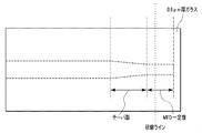
- the spot size conversion unit may have glass (here, 6 ⁇ m thick glass) at the tip as shown in FIG. 7A, or may have a shape as shown in FIG. 7B after processing by means such as polishing or dicing. .
- Non-Patent Document 1 Although a conventional spot size enlargement unit of such a shape has been proposed that is limited to lens coupling in space, such alignment of the optical waveguide array is required because alignment is required for each optical waveguide. It is not easy to apply the structure, and the manufacturing cost is also high (see Non-Patent Document 1).
- the method using UV bonding and fixing described in the first embodiment has a record of producing a product with up to several tens of silica optical waveguides, and is low cost and highly reliable.
- FIG. 9 shows the optical waveguide angle dependency of the reflection loss of the Si optical waveguide with an MFD: 1.0 ⁇ m whose spot size is hardly expanded and the optical waveguide of the MFD: 5.0 ⁇ m Si photonics lightwave circuit.
- the result shown in FIG. 9 is simply calculated by reflection (Gaussian coupling) at the interface between the optical waveguide of the Si photonics lightwave circuit and the adhesive with respect to the incident beam, and adding dB of the Fresnel reflection perpendicular thereto Calculated.
- the calculation conditions were a wavelength of 1.55 ⁇ m, and an equivalent refractive index of 1.455 at the exit portion of the optical waveguide of the Si photonics lightwave circuit. This is a value determined on the assumption that the reflection loss is 30 dB or more at an oblique inclination angle of 5 degrees in the calculation of the reflection.
- the refractive index of the UV adhesive was 1.45
- the MFD of the light emitted from the Si photonics light wave circuit was 5.0 ⁇ m (spot size 2.5 ⁇ m).
- the reflection loss increases as the MFD is thus expanded.
- the waveguide angle should be 5 degrees or more, since 30 dB or more is usually desirable.
- an antireflective film (AR film) is also used to prevent such end face reflection, it is a multilayer film formation in which the refractive index and the film thickness are strictly controlled, which requires cost and time.
- AR film antireflective film
- the method of the oblique waveguide of the present invention is excellent in anti-reflection effect at low cost and without wavelength dependency, though lensless and array collective connection is possible.
- FIG. 10 shows the coupling loss reduction effect by the spot size expansion of the optical waveguide of the Si photonics lightwave circuit.
- the calculation conditions are: wavelength 1.55 ⁇ m, optical waveguide spot size 2.5 ⁇ m of Si photonics lightwave circuit, optical fiber spot size 4.0 ⁇ m (DSF fiber typical value), distance between Si photonics lightwave circuit-optical fiber is 10 ⁇ m .
Landscapes
- Physics & Mathematics (AREA)
- General Physics & Mathematics (AREA)
- Optics & Photonics (AREA)
- Engineering & Computer Science (AREA)
- Microelectronics & Electronic Packaging (AREA)
- Chemical & Material Sciences (AREA)
- Crystallography & Structural Chemistry (AREA)
- Power Engineering (AREA)
- Optical Couplings Of Light Guides (AREA)
- Optical Integrated Circuits (AREA)
Abstract
光ファイバアレイとの接続を有する、高密度に実装可能な光モジュールを提供すること。ボード(101)に2つの30mm角のパッケージモジュール(102、105)が実装され、パッケージモジュール(102)に実装された20mm角のSiフォトニクス光波回路(103)の光導波路と光ファイバブロック(15×10mm)(104)に固定された光ファイバアレイ(106)とが接続されている。また、Siフォトニクス光波回路(103)の光導波路の出射端面は、パッケージモジュール(102)の実装面に対して垂直である。本実施形態では、Siフォトニクス光波回路(103)の光導波路を右側端面に垂直な方向から、適当な角度、例えば20度傾けている。そして、光ファイバブロック(104)も、各光ファイバをSiフォトニクス光波回路(103)と接続する端面に垂直な方向から20度傾けて固定している。
Description
本発明は、光ファイバとの接続を有するSiフォトニクス光波回路を含む光モジュールに関する。
現在、Siフォトニクス素子を用いた光モジュール、例えば、光変調器、光受信機、両者を組み合わせたコヒーレント光サブアッセンブリ(COSA)等の開発が盛んに行われている。Siフォトニクス素子は、半導体として広く使用され、シリコン酸化膜やポリマーに比べ屈折率が非常に大きいシリコンをコア材料に用いた微小な光導波路を作製した光波回路からなる。このSiコアからなる光導波路は、従来PLCより比屈折率が10倍以上高く、モードフィールド径(Mode field diameter:MFD)は1/10以下でミクロンオーダの閉じ込めが強く、最小曲げ半径が小さい(~5μm)。そのためSiフォトニクス素子自体が、従来光デバイスに比べ超小型の特徴があり、従来以上に、小型高密度な光トランシーバ等の光モジュールの実現が期待されている。
そのSiフォトニクス素子、小型光部品は、LDモジュール等、他の光ファイバピグテールモジュールと組み合わせ用いられることが多く、個々のモジュールのみならず、各モジュールを、光ファイバ等で接続し組み合わせて実装するサブボード、あるいはそれらを収容するケース、例えばCFP2等のサイズに制約のあるケースの、全体の小型化が求められている。
Siフォトニクス素子の光導波路のSiコアは、SiO2膜により形成されたコアより細く、サブミクロンオーダー角である。このような細い光導波路は、通常の光ファイバとそのまま接続すると光結合損失が大きいので、光導波路端から出射される光のモードフィールド径を拡大する必要がある。
即ち、Siフォトニクス光波回路内は曲率半径5μm程度で集積されて機能の高密度化が進み、光ファイバや電気回路の多アレイ化が進んでいる一方で、光ファイバの曲率は例えば15mm程度であり、Siフォトニクス光波回路を小型すると共に、外部光ファイバの取り回し部も含むモジュール群も同様に小型にする必要がある。
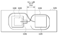
図11に、従来のSiフォトニクス素子の典型例を示す。同一のボード1101に2つのパッケージモジュール1102、1105が実装されている。ここではSiフォトニクス光波回路1103は20mm角であり、30mm角のパッケージモジュール1102に実装されている。そしてSiフォトニクス光波回路1103から図右側で、固定した光ファイバ2心フェルール(8×10mm)1104で固定された光ファイバアレイ1106と接続している。Siフォトニクス光波回路1103の2心の光導波路を光ファイバアレイ1106と接続する手段としては、レンズを介してYAG溶接で光ファイバフェルールを固定する方法や、メタルコートした光ファイバを半田固定する方法等がある。
Jaime Cardenas, "High Coupling Efficiency Etched Facet Tapers in Silicon Waveguides," IEEE Photon. Lett., Vol.26, p.2380, 2014.
ここでSiフォトニクス光波回路1103の光導波路は右側辺に垂直であり、光ファイバアレイ1106も右側辺に対して垂直に接続されているため、光ファイバアレイ1106が右側光モジュール1105と接触する。また、通常、放熱等でパッケージモジュール1102、1105の基板面に対して垂直方向には光ファイバを通すための空間はなく、パッケージモジュールと光ファイバとは重ねられない。そのため、光ファイバを図のようにパッケージモジュール1105の周囲を通すためには、光ファイバの曲率15mmも考慮して、パッケージモジュール1102、1105は一定距離離してレイアウトする必要がある。レイアウトの一例では、パッケージモジュール1102、1105間は27mm以上の間隔を空ける必要があった。
このように、従来、Siフォトニクス光波回路を含むモジュールに光ファイバを接続する場合、モジュール間の間隙がモジュールサイズと同程度に大きく、これらモジュールを小型にレイアウトできないという課題があった。
本発明は、このような課題に鑑みてなされたもので、その目的とするところは、光ファイバアレイとの接続を有する、高密度に実装可能な光モジュールを提供することにある。
上記の課題を解決するために、本発明は、光モジュールであって、SiコアおよびSiO2クラッドからなる光導波路を有するSiフォトニクス光波回路であって、前記光導波路は、出射端面において前記出射端面に垂直な方向に対して斜め傾け角度を有し、前記光導波路の前記出射端面における中心は、前記Siフォトニクス光波回路の前記出射端面を含む側面の中心よりも前記光導波路が傾いている方向にシフトしている、Siフォトニクス光波回路と、前記光導波路と同じ斜め傾け角度で光ファイバアレイを固定する光ファイバブロックと、を備えたことを特徴とする。
本発明の別の態様では、前記Siフォトニクス光波回路の前記光導波路の出射端面は、前記Siフォトニクス光波回路の実装面に対して垂直であることを特徴とする。
本発明の別の態様では、前記Siフォトニクス光波回路の前記光導波路は、複数の光導波路が平行に配置された光導波路アレイであることを特徴とする。
本発明の別の態様では、前記Siフォトニクス光波回路の前記光導波路は、前記Siコアの幅が前記出射端面に向けて細くなるテーパ部からなるスポットサイズ拡大部を含むことを特徴とする。
本発明の別の態様では、前記斜め傾け角度は、5度以上50度以下であることを特徴とする。
本発明の別の態様では、前記Siフォトニクス光波回路の前記光導波路は、前記Siコアの幅が前記出射端面に向けて細くなるテーパ部の先端に幅が一定な導波路を備えることを特徴とする。
本発明では、光ファイバアレイとの接続を有する光モジュールを高密度に実装することが可能になる。
以下、本発明の実施の形態について、詳細に説明する。
(実施形態1)
図1に、本発明の実施形態1に係る光モジュールの構成を示す。本実施形態では、図11の構成と同様に、ボード101に2つの30mm角のパッケージモジュール102、105が実装され、パッケージモジュール102に実装された20mm角のSiフォトニクス光波回路103の光導波路と光ファイバブロック(15×10mm)104に固定された光ファイバアレイ106とが接続されている。また、Siフォトニクス光波回路103の光導波路の出射端面は、ボード101とパッケージモジュール102が接する面であるパッケージモジュール102の実装面、又は、パッケージモジュール102とSiフォトニクス光波回路103とが接するSiフォトニクス光波回路103の実装面に対して垂直である。ここで中心導波路、又は両端の光導波路間の中心の端面上の位置は、従来例との比較のため、図11の構成と同様にパッケージモジュール102の出射端面にあたる右側辺の中心(上下から15mmの点)とした。
図1に、本発明の実施形態1に係る光モジュールの構成を示す。本実施形態では、図11の構成と同様に、ボード101に2つの30mm角のパッケージモジュール102、105が実装され、パッケージモジュール102に実装された20mm角のSiフォトニクス光波回路103の光導波路と光ファイバブロック(15×10mm)104に固定された光ファイバアレイ106とが接続されている。また、Siフォトニクス光波回路103の光導波路の出射端面は、ボード101とパッケージモジュール102が接する面であるパッケージモジュール102の実装面、又は、パッケージモジュール102とSiフォトニクス光波回路103とが接するSiフォトニクス光波回路103の実装面に対して垂直である。ここで中心導波路、又は両端の光導波路間の中心の端面上の位置は、従来例との比較のため、図11の構成と同様にパッケージモジュール102の出射端面にあたる右側辺の中心(上下から15mmの点)とした。
一方、本実施形態では、Siフォトニクス光波回路103の光導波路を右側端面に垂直な方向から、適当な角度、例えば20度傾けている。そして、光ファイバブロック104も、各光ファイバをSiフォトニクス光波回路103と接続する端面に垂直な方向から20度傾けて固定している。
後述のように、ここでSiフォトニクス光波回路103の光導波路は端面でMFDを拡大し、光ファイバと同じフィールド径にしている。そのため、Siフォトニクス光波回路103の光導波路と光ファイバは、接続端面に垂直な方向から同一傾け角度を有し、同一直線上での接続が可能である。このようなSiフォトニクス光波回路103、光ファイバブロック104を用いることにより、パッケージモジュール102、105間のパッケージ間のギャップは16mmと、図11に示す従来例の27mmに比べ大幅に低減でき、パッケージモジュール長30mmの約半分に低減することができる。
(実施形態2)
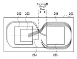
図2に、本発明の実施形態2に係る光モジュールの構成を示す。本実施形態では、実施形態1と同様に、シャーシ201に2つの30mm角のパッケージモジュール202、205が実装され、パッケージモジュール202に実装された20mm角のSiフォトニクス光波回路203の光導波路と光ファイバブロック(15×10mm)204に固定された光ファイバアレイ206とが接続されている。
図2に、本発明の実施形態2に係る光モジュールの構成を示す。本実施形態では、実施形態1と同様に、シャーシ201に2つの30mm角のパッケージモジュール202、205が実装され、パッケージモジュール202に実装された20mm角のSiフォトニクス光波回路203の光導波路と光ファイバブロック(15×10mm)204に固定された光ファイバアレイ206とが接続されている。
実施形態2では、Siフォトニクス光波回路の光導波路位置をパッケージモジュール中央付近から光導波路を傾けた側(図上側)にシフトさせることによって、実施形態1の構成よりもさらにパッケージ間のギャップを狭くしている。図2に示すように、Siフォトニクス光波回路203の中心導波路を、パッケージモジュール202の出射端面にあたる右側辺の中心から図上側に5mmシフトさせ、光ファイバブロック204も同様に図上側に5mmシフトさせた。これにより、パッケージモジュール202、205間は16mmから11mmに短縮できる。
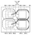
図3に、図2の構成を2つ同一シャーシ301上に実装した構成を示す。このように、本発明の光モジュールを用いることにより、より高密度な実装が可能になる。
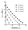
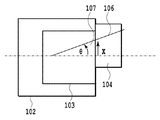
ここで図4Aに、Siフォトニクス光波回路の光導波路と光ファイバブロックの接続部を示し、図4Bに、斜め傾け角度θに対するモジュール間隔を示す。図4Bの結果は、光導波路および光ファイバの斜め傾け角度をθ、光導波路出射位置の点線からの距離をXとし、光ファイバの最小曲げ半径を15mmとして計算によって求めた。光ファイバが最小曲げ半径をもつのは、モジュール間ギャップを最小化するため、少なくとも、光ファイバブロック側から光ファイバに沿って数えて最初の2箇所の曲げである、パッケージモジュール間の曲げにおいてである。図1に示す構成はX=0mm、θ=20度に対応し、図2に示す構成はX=5mm、θ=20度に対応する。
ここで実際のボードや100Gb/s伝送用の光トランシーバ規格の一つである第2世代のCFP2(幅41.5mm×長さ106mm×高さ12.4mm)といったシャーシにモジュールを納めるには、1mmでもボードサイズを低減するよう要請されることもある。図4Bに示す通り、パッケージモジュールの中心位置(X=0mm)からシフトし、光導波路出射位置のシフト方向と同一方向に光導波路を傾けた場合に光モジュール間隔を低減することが可能である。さらに、5度以上に光導波路を傾けることが小型化のためにはより好適である。
一方、50度以上、光導波路が傾いていると、接着層厚の変動等により光軸ズレにつながるリスクがある。
そのため、光導波路角度については、5度から50度傾けることにより、光モジュール間のモジュール間隔を狭めることができ、高密度ボードを作製するのにより有利である。
図5Aに、Siフォトニクス光波回路の光導波路と光ファイバブロックの接続部を示し、図5Bに、光ファイバの最小曲げ半径を5mmとした場合の斜め傾け角度θに対するモジュール間隔を示す。この場合も、光ファイバが最小曲げ半径をもつのは、モジュール間ギャップを最小化するため、少なくとも、光ファイバブロック側から光ファイバに沿って数えて最初の2箇所の曲げである、パッケージモジュール間の曲げにおいてであり、最小曲げ半径が15mmの場合と同様の効果が得られる。
<スポットサイズ変換部>
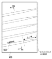
図6Aに、Siフォトニクス光波回路の光導波路アレイの拡大図を示す。また、図6BにSiフォトニクス光波回路の光導波路アレイの断面図を示す。Si基板401上にSiコア402、SiO2クラッド403からなる光導波路が形成されており、各光導波路幅は、500nm、テーパ部長は100μm、テーパ部の先端の幅は約160nmである(非特許文献1参照)。このスポットサイズ変換部により、出射端面付近でMFDは、5.0μmに広がる。
図6Aに、Siフォトニクス光波回路の光導波路アレイの拡大図を示す。また、図6BにSiフォトニクス光波回路の光導波路アレイの断面図を示す。Si基板401上にSiコア402、SiO2クラッド403からなる光導波路が形成されており、各光導波路幅は、500nm、テーパ部長は100μm、テーパ部の先端の幅は約160nmである(非特許文献1参照)。このスポットサイズ変換部により、出射端面付近でMFDは、5.0μmに広がる。
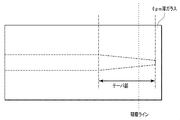
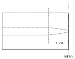
尚、このスポットサイズ変換部は、図7Aのように先端にガラス(ここでは6μm厚ガラス)があってもよいし、研磨、あるいはダイシング等の手段で加工して図7Bのような形状でもよい。
但し、図7Bのような構造の場合、加工位置のばらつきにより、端面位置にばらつきが生じると、それに伴ってテーパ先端幅にもばらつきが生じて、出射MFDがばらつくリスクがある。そこで、図8Aに示すようにテーパ先端に幅が一定な構造を設ける。このような構造では、幅が一定な構造部分において研磨等の加工をすれば、右側からの削り深さにばらつきがあっても、加工後の出射端面における光導波路の幅は一定になる。この構造では、加工位置にばらつきがあってもMFDが設計値からずれない、スポットサイズ拡大が可能である。
従来のこのような形状のスポットサイズ拡大部は、空間のレンズ結合に限ったものは提案されているが、光導波路毎に調心等が必要になるため、光導波路アレイに対してこのような構造を適用するのは容易ではなく、製造コストも高くなる(非特許文献1参照)。
それに対して実施形態1に記載した、UV接着固定を用いた方法は、石英系光導波路でも数十心までの商品を製造した実績があり、低コストで高信頼である。
<Siフォトニクス光波回路-光ファイバ、斜め導波路、反射防止効果>
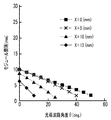
このスポットサイズ拡大の効果は、反射損失を高くして有害な反射戻り光を抑える効果もある。図9に、スポットサイズがほとんど拡大されていないMFD:1.0μmのSi光導波路と、MFD:5.0μmのSiフォトニクス光波回路の光導波路との反射損失の光導波路角度依存性を示す。図9に示す結果は、単純に、入射ビームに対する反射ビームを、Siフォトニクス光波回路の光導波路と接着剤との界面での反射(ガウス結合)で計算し、それに垂直のフレネル反射をdB加算して算出したものである。
このスポットサイズ拡大の効果は、反射損失を高くして有害な反射戻り光を抑える効果もある。図9に、スポットサイズがほとんど拡大されていないMFD:1.0μmのSi光導波路と、MFD:5.0μmのSiフォトニクス光波回路の光導波路との反射損失の光導波路角度依存性を示す。図9に示す結果は、単純に、入射ビームに対する反射ビームを、Siフォトニクス光波回路の光導波路と接着剤との界面での反射(ガウス結合)で計算し、それに垂直のフレネル反射をdB加算して算出したものである。
計算条件は、波長1.55μm、Siフォトニクス光波回路の光導波路の出射部での等価屈折率1.455とした。これは、反射の計算において、斜め傾き角度が5度で反射損が30dB以上になると仮定して決めた値である。また、UV接着剤の屈折率は1.45、Siフォトニクス光波回路からの出射のMFDは5.0μm(スポットサイズ2.5μm)とした。
このようにMFDを拡大すると反射損が増大する。通常30dB以上が望ましいため、導波路角度は5度以上が必要である。
このような端面の反射防止には、反射防止膜(AR膜)も用いられるが、屈折率と膜厚を厳密に制御した多層膜形成であり、コストと時間を要する。加えて、波長依存性もあるため、使用波長帯に合わせた薄膜を形成する必要がある。これに対し、本発明の斜め導波路の方法は、レンズレスで、かつアレイ一括接続が可能でありながら、低コストで波長依存性のない優れた反射防止効果を奏する。
<Siフォトニクス光波回路-光ファイバ、SSC拡大、損失低減効果>
図10に、Siフォトニクス光波回路の光導波路のスポットサイズ拡大による結合損失低減効果を示す。計算条件は、波長1.55μm、Siフォトニクス光波回路の光導波路スポットサイズ2.5μm、光ファイバスポットサイズ4.0μm(DSFファイバ典型値)、Siフォトニクス光波回路-光ファイバ間の間隔は10μmとした。このようにスポットサイズを拡大することにより、結合損失を大幅に低減することができる。
図10に、Siフォトニクス光波回路の光導波路のスポットサイズ拡大による結合損失低減効果を示す。計算条件は、波長1.55μm、Siフォトニクス光波回路の光導波路スポットサイズ2.5μm、光ファイバスポットサイズ4.0μm(DSFファイバ典型値)、Siフォトニクス光波回路-光ファイバ間の間隔は10μmとした。このようにスポットサイズを拡大することにより、結合損失を大幅に低減することができる。
101 ボード
102、105 パッケージモジュール
103 Siフォトニクス光波回路
104 光ファイバブロック
106 光ファイバアレイ
201、301-1、302-2 シャーシ
202、205、302-1、302-2、305-1、305-2 パッケージモジュール
203、303-1、303-2 Siフォトニクス光波回路
204、304-1、304-2 光ファイバブロック
206、306-1、306-2 光ファイバアレイ
401 Si基板
402 Siコア
403 SiO2クラッド
1101 ボード
1102、1105 パッケージモジュール
1103 Siフォトニクス光波回路
1104 光ファイバブロック
1106 光ファイバアレイ
102、105 パッケージモジュール
103 Siフォトニクス光波回路
104 光ファイバブロック
106 光ファイバアレイ
201、301-1、302-2 シャーシ
202、205、302-1、302-2、305-1、305-2 パッケージモジュール
203、303-1、303-2 Siフォトニクス光波回路
204、304-1、304-2 光ファイバブロック
206、306-1、306-2 光ファイバアレイ
401 Si基板
402 Siコア
403 SiO2クラッド
1101 ボード
1102、1105 パッケージモジュール
1103 Siフォトニクス光波回路
1104 光ファイバブロック
1106 光ファイバアレイ
Claims (6)
- SiコアおよびSiO2クラッドからなる光導波路を有するSiフォトニクス光波回路であって、前記光導波路は、出射端面において前記出射端面に垂直な方向に対して斜め傾け角度を有し、前記光導波路の前記出射端面における中心は、前記Siフォトニクス光波回路の前記出射端面を含む側面の中心よりも前記光導波路が傾いている方向にシフトしている、Siフォトニクス光波回路と、
前記光導波路と同じ斜め傾け角度で光ファイバアレイを固定する光ファイバブロックと、
を備えたことを特徴とする光モジュール。 - 前記Siフォトニクス光波回路の前記光導波路の出射端面は、前記Siフォトニクス光波回路の実装面に対して垂直であることを特徴とする請求項1記載の光モジュール。
- 前記Siフォトニクス光波回路の前記光導波路は、複数の光導波路が平行に配置された光導波路アレイであることを特徴とする請求項1又は2に記載の光モジュール。
- 前記Siフォトニクス光波回路の前記光導波路は、前記Siコアの幅が前記出射端面に向けて細くなるテーパ部からなるスポットサイズ拡大部を含むことを特徴とする請求項1又は2に記載の光モジュール。
- 前記斜め傾け角度は、5度以上50度以下であることを特徴とする請求項1又は2に記載の光モジュール。
- 前記Siフォトニクス光波回路の前記光導波路は、前記Siコアの幅が前記出射端面に向けて細くなるテーパ部の先端に幅が一定な導波路を備えることを特徴とする請求項4に記載の光モジュール。
Priority Applications (3)
| Application Number | Priority Date | Filing Date | Title |
|---|---|---|---|
| DE112017002464.1T DE112017002464B4 (de) | 2016-05-13 | 2017-05-12 | Optikmodul |
| US16/099,955 US10649147B2 (en) | 2016-05-13 | 2017-05-12 | Optical module |
| CA3023857A CA3023857C (en) | 2016-05-13 | 2017-05-12 | Optical module |
Applications Claiming Priority (2)
| Application Number | Priority Date | Filing Date | Title |
|---|---|---|---|
| JP2016-097427 | 2016-05-13 | ||
| JP2016097427A JP6649843B2 (ja) | 2016-05-13 | 2016-05-13 | 光回路 |
Publications (1)
| Publication Number | Publication Date |
|---|---|
| WO2017195892A1 true WO2017195892A1 (ja) | 2017-11-16 |
Family
ID=60266734
Family Applications (1)
| Application Number | Title | Priority Date | Filing Date |
|---|---|---|---|
| PCT/JP2017/018054 Ceased WO2017195892A1 (ja) | 2016-05-13 | 2017-05-12 | 光モジュール |
Country Status (6)
| Country | Link |
|---|---|
| US (1) | US10649147B2 (ja) |
| JP (1) | JP6649843B2 (ja) |
| CN (2) | CN107367802B (ja) |
| CA (1) | CA3023857C (ja) |
| DE (1) | DE112017002464B4 (ja) |
| WO (1) | WO2017195892A1 (ja) |
Families Citing this family (5)
| Publication number | Priority date | Publication date | Assignee | Title |
|---|---|---|---|---|
| JP6649843B2 (ja) | 2016-05-13 | 2020-02-19 | Nttエレクトロニクス株式会社 | 光回路 |
| US11275211B2 (en) * | 2019-06-18 | 2022-03-15 | Cisco Technology, Inc. | Fiber array unit with unfinished endface |
| JP7360695B2 (ja) | 2019-10-02 | 2023-10-13 | 株式会社中原光電子研究所 | 光接続装置 |
| JP2021113907A (ja) * | 2020-01-20 | 2021-08-05 | 住友電気工業株式会社 | 光トランシーバ |
| JP2021120704A (ja) * | 2020-01-30 | 2021-08-19 | 住友電気工業株式会社 | 光トランシーバ |
Citations (7)
| Publication number | Priority date | Publication date | Assignee | Title |
|---|---|---|---|---|
| JPH04163405A (ja) * | 1990-10-26 | 1992-06-09 | Fujikura Ltd | 光カプラ及びその製造方法 |
| JPH0491311U (ja) * | 1990-12-27 | 1992-08-10 | ||
| JPH07128545A (ja) * | 1993-11-05 | 1995-05-19 | Hitachi Cable Ltd | 光導波路と光ファイバとの接続方法 |
| JP2002228863A (ja) * | 2001-02-06 | 2002-08-14 | Kddi Submarine Cable Systems Inc | 光結合構造 |
| JP2005148538A (ja) * | 2003-11-18 | 2005-06-09 | Toyoda Mach Works Ltd | 光導波路及びレーザ発光装置 |
| US20120156369A1 (en) * | 2010-12-16 | 2012-06-21 | Electronics And Telecommunications Research Institute | Method of forming optical coupler |
| US20140177995A1 (en) * | 2012-12-20 | 2014-06-26 | Edris M. Mohammed | Optical photonic circuit coupling |
Family Cites Families (13)
| Publication number | Priority date | Publication date | Assignee | Title |
|---|---|---|---|---|
| JPH0794803B2 (ja) | 1990-08-01 | 1995-10-11 | 本田技研工業株式会社 | 水平シリンダを備えるエンジンの潤滑油路構造及びそのエンジンを搭載してなる船外機 |
| JPH05113517A (ja) * | 1991-10-22 | 1993-05-07 | Nippon Telegr & Teleph Corp <Ntt> | 光導波路と光フアイバとの接続構造 |
| US5960131A (en) * | 1998-02-04 | 1999-09-28 | Hewlett-Packard Company | Switching element having an expanding waveguide core |
| JP2001324647A (ja) * | 2000-05-16 | 2001-11-22 | Fujikura Ltd | 光ファイバアレイ、光導波路チップ及びこれらを接続した光モジュール |
| JP4163405B2 (ja) * | 2001-09-27 | 2008-10-08 | 株式会社日本触媒 | アルカノールアミンの製造方法 |
| CN1195326C (zh) | 2002-04-26 | 2005-03-30 | 中国科学院半导体研究所 | 硅基光子集成的器件及制作方法 |
| CN1271765C (zh) * | 2004-04-02 | 2006-08-23 | 华中科技大学 | 一种集成模斑变换器的脊型波导偏振无关半导体光放大器 |
| CN102118525B (zh) * | 2009-12-30 | 2013-07-03 | 北京大唐高鸿数据网络技术有限公司 | 一种基于VoIP的矿用扩播电话系统 |
| JP5825315B2 (ja) * | 2013-09-30 | 2015-12-02 | 住友大阪セメント株式会社 | 光学素子モジュール |
| CN106133999A (zh) * | 2014-02-06 | 2016-11-16 | 斯考皮欧技术有限公司 | 用于波导与光纤耦合的集成式多级锥形耦合器 |
| JP6290742B2 (ja) * | 2014-07-24 | 2018-03-07 | 日本電信電話株式会社 | 光回路部品、および光回路部品と光ファイバとの接続構造 |
| JP2016053679A (ja) * | 2014-09-04 | 2016-04-14 | 富士通株式会社 | 光ファイバの接続構造、光ファイバホルダおよび光ファイバの接続方法 |
| JP6649843B2 (ja) * | 2016-05-13 | 2020-02-19 | Nttエレクトロニクス株式会社 | 光回路 |
-
2016
- 2016-05-13 JP JP2016097427A patent/JP6649843B2/ja active Active
-
2017
- 2017-05-12 US US16/099,955 patent/US10649147B2/en active Active
- 2017-05-12 CN CN201710338459.6A patent/CN107367802B/zh active Active
- 2017-05-12 DE DE112017002464.1T patent/DE112017002464B4/de active Active
- 2017-05-12 CA CA3023857A patent/CA3023857C/en active Active
- 2017-05-12 CN CN201720534246.6U patent/CN206833034U/zh not_active Withdrawn - After Issue
- 2017-05-12 WO PCT/JP2017/018054 patent/WO2017195892A1/ja not_active Ceased
Patent Citations (7)
| Publication number | Priority date | Publication date | Assignee | Title |
|---|---|---|---|---|
| JPH04163405A (ja) * | 1990-10-26 | 1992-06-09 | Fujikura Ltd | 光カプラ及びその製造方法 |
| JPH0491311U (ja) * | 1990-12-27 | 1992-08-10 | ||
| JPH07128545A (ja) * | 1993-11-05 | 1995-05-19 | Hitachi Cable Ltd | 光導波路と光ファイバとの接続方法 |
| JP2002228863A (ja) * | 2001-02-06 | 2002-08-14 | Kddi Submarine Cable Systems Inc | 光結合構造 |
| JP2005148538A (ja) * | 2003-11-18 | 2005-06-09 | Toyoda Mach Works Ltd | 光導波路及びレーザ発光装置 |
| US20120156369A1 (en) * | 2010-12-16 | 2012-06-21 | Electronics And Telecommunications Research Institute | Method of forming optical coupler |
| US20140177995A1 (en) * | 2012-12-20 | 2014-06-26 | Edris M. Mohammed | Optical photonic circuit coupling |
Non-Patent Citations (2)
| Title |
|---|
| CARDENAS, J. ET AL.: "High Coupling Efficiency Etched Facet Tapers in Silicon Waveguides", IEEE PHOTONICS TECHNOLOGY LETTERS, vol. 26, no. 23, 1 December 2014 (2014-12-01), pages 2380 - 2382, XP011563526 * |
| KOJI YAMADA ET AL.: "Chip-jo Hikari Inter Connection e Muketa Silicon Saisen Hikari Doharo Gijutsu", 2006 NEN (HEISEI 18 NEN) SHUKI DAI 67 KAI EXTENDED ABSTRACTS; THE JAPAN SOCIETY OF APPLIED PHYSICS THE JAPAN SOCIETY OF APPLIED PHYSICS, September 2006 (2006-09-01), pages 107 * |
Also Published As
| Publication number | Publication date |
|---|---|
| DE112017002464B4 (de) | 2024-01-04 |
| CA3023857A1 (en) | 2017-11-16 |
| US20190353844A1 (en) | 2019-11-21 |
| JP6649843B2 (ja) | 2020-02-19 |
| CN107367802A (zh) | 2017-11-21 |
| CA3023857C (en) | 2021-07-13 |
| DE112017002464T5 (de) | 2019-01-31 |
| CN107367802B (zh) | 2019-10-11 |
| JP2017203966A (ja) | 2017-11-16 |
| US10649147B2 (en) | 2020-05-12 |
| CN206833034U (zh) | 2018-01-02 |
Similar Documents
| Publication | Publication Date | Title |
|---|---|---|
| US8639073B2 (en) | Fiber coupling technique on a waveguide | |
| US11105981B2 (en) | Optical connectors and detachable optical connector assemblies for optical chips | |
| KR101508619B1 (ko) | 광 신호를 라우팅하기 위한 시스템 및 방법 | |
| US9086551B2 (en) | Double mirror structure for wavelength division multiplexing with polymer waveguides | |
| JP6649843B2 (ja) | 光回路 | |
| US9575257B2 (en) | Optical device, optical processing device, method for fabricating optical device | |
| WO2013117555A1 (en) | An optical coupling arrangement | |
| CN106461895A (zh) | 自由空间光耦合系统和装置 | |
| CN112904499A (zh) | 半导体激光器和平面光波导耦合结构、光路系统及制造方法 | |
| JP4948185B2 (ja) | 平面光波回路 | |
| JP7601113B2 (ja) | 光接続構造、光モジュールおよび光接続構造の製造方法 | |
| JP2023041329A (ja) | 光集積素子、光集積回路ウエハ及び光集積素子の製造方法 | |
| WO2014199831A1 (ja) | 光路変更素子、光路変更素子の接続構造、光源デバイスおよび光実装デバイス | |
| US20230236368A1 (en) | Optical module package using bi-angled silica waveguide | |
| CN110989079B (zh) | 一种空气包层su8阵列波导光栅 | |
| WO2019176561A1 (ja) | ファイバモジュール | |
| JP4549949B2 (ja) | 光学素子 | |
| JP4277840B2 (ja) | 光導波路デバイスの製造方法 | |
| JP2016212414A (ja) | 導波路用結合回路 | |
| JP5772436B2 (ja) | 光結合器及び光デバイス | |
| JP2009037054A (ja) | 光モジュール及びその製造方法 | |
| CN121596461A (zh) | 一种二维光栅耦合器 | |
| Hendrickx et al. | Towards flexible routing schemes for polymer optical interconnections on printed circuit boards | |
| JP2004286779A (ja) | 光増幅器 | |
| JPWO2024171712A5 (ja) |
Legal Events
| Date | Code | Title | Description |
|---|---|---|---|
| ENP | Entry into the national phase |
Ref document number: 3023857 Country of ref document: CA |
|
| 121 | Ep: the epo has been informed by wipo that ep was designated in this application |
Ref document number: 17796250 Country of ref document: EP Kind code of ref document: A1 |
|
| 122 | Ep: pct application non-entry in european phase |
Ref document number: 17796250 Country of ref document: EP Kind code of ref document: A1 |