WO2017195701A1 - 圧電素子用駆動回路 - Google Patents
圧電素子用駆動回路 Download PDFInfo
- Publication number
- WO2017195701A1 WO2017195701A1 PCT/JP2017/017236 JP2017017236W WO2017195701A1 WO 2017195701 A1 WO2017195701 A1 WO 2017195701A1 JP 2017017236 W JP2017017236 W JP 2017017236W WO 2017195701 A1 WO2017195701 A1 WO 2017195701A1
- Authority
- WO
- WIPO (PCT)
- Prior art keywords
- piezoelectric element
- output terminal
- control signal
- drive voltage
- drive
- Prior art date
- Legal status (The legal status is an assumption and is not a legal conclusion. Google has not performed a legal analysis and makes no representation as to the accuracy of the status listed.)
- Ceased
Links
Images











Classifications
-
- F—MECHANICAL ENGINEERING; LIGHTING; HEATING; WEAPONS; BLASTING
- F04—POSITIVE - DISPLACEMENT MACHINES FOR LIQUIDS; PUMPS FOR LIQUIDS OR ELASTIC FLUIDS
- F04B—POSITIVE-DISPLACEMENT MACHINES FOR LIQUIDS; PUMPS
- F04B43/00—Machines, pumps, or pumping installations having flexible working members
- F04B43/02—Machines, pumps, or pumping installations having flexible working members having plate-like flexible members, e.g. diaphragms
- F04B43/04—Pumps having electric drive
- F04B43/043—Micropumps
- F04B43/046—Micropumps with piezoelectric drive
-
- F—MECHANICAL ENGINEERING; LIGHTING; HEATING; WEAPONS; BLASTING
- F04—POSITIVE - DISPLACEMENT MACHINES FOR LIQUIDS; PUMPS FOR LIQUIDS OR ELASTIC FLUIDS
- F04B—POSITIVE-DISPLACEMENT MACHINES FOR LIQUIDS; PUMPS
- F04B17/00—Pumps characterised by combination with, or adaptation to, specific driving engines or motors
- F04B17/003—Pumps characterised by combination with, or adaptation to, specific driving engines or motors driven by piezoelectric means
-
- F—MECHANICAL ENGINEERING; LIGHTING; HEATING; WEAPONS; BLASTING
- F04—POSITIVE - DISPLACEMENT MACHINES FOR LIQUIDS; PUMPS FOR LIQUIDS OR ELASTIC FLUIDS
- F04B—POSITIVE-DISPLACEMENT MACHINES FOR LIQUIDS; PUMPS
- F04B49/00—Control, e.g. of pump delivery, or pump pressure of, or safety measures for, machines, pumps, or pumping installations, not otherwise provided for, or of interest apart from, groups F04B1/00 - F04B47/00
- F04B49/06—Control using electricity
-
- F—MECHANICAL ENGINEERING; LIGHTING; HEATING; WEAPONS; BLASTING
- F04—POSITIVE - DISPLACEMENT MACHINES FOR LIQUIDS; PUMPS FOR LIQUIDS OR ELASTIC FLUIDS
- F04B—POSITIVE-DISPLACEMENT MACHINES FOR LIQUIDS; PUMPS
- F04B49/00—Control, e.g. of pump delivery, or pump pressure of, or safety measures for, machines, pumps, or pumping installations, not otherwise provided for, or of interest apart from, groups F04B1/00 - F04B47/00
- F04B49/06—Control using electricity
- F04B49/065—Control using electricity and making use of computers
-
- H—ELECTRICITY
- H02—GENERATION; CONVERSION OR DISTRIBUTION OF ELECTRIC POWER
- H02N—ELECTRIC MACHINES NOT OTHERWISE PROVIDED FOR
- H02N2/00—Electric machines in general using piezoelectric effect, electrostriction or magnetostriction
- H02N2/02—Electric machines in general using piezoelectric effect, electrostriction or magnetostriction producing linear motion, e.g. actuators; Linear positioners ; Linear motors
- H02N2/06—Drive circuits; Control arrangements or methods
-
- H—ELECTRICITY
- H10—SEMICONDUCTOR DEVICES; ELECTRIC SOLID-STATE DEVICES NOT OTHERWISE PROVIDED FOR
- H10N—ELECTRIC SOLID-STATE DEVICES NOT OTHERWISE PROVIDED FOR
- H10N30/00—Piezoelectric or electrostrictive devices
- H10N30/20—Piezoelectric or electrostrictive devices with electrical input and mechanical output, e.g. functioning as actuators or vibrators
-
- H—ELECTRICITY
- H10—SEMICONDUCTOR DEVICES; ELECTRIC SOLID-STATE DEVICES NOT OTHERWISE PROVIDED FOR
- H10N—ELECTRIC SOLID-STATE DEVICES NOT OTHERWISE PROVIDED FOR
- H10N30/00—Piezoelectric or electrostrictive devices
- H10N30/30—Piezoelectric or electrostrictive devices with mechanical input and electrical output, e.g. functioning as generators or sensors
-
- H—ELECTRICITY
- H10—SEMICONDUCTOR DEVICES; ELECTRIC SOLID-STATE DEVICES NOT OTHERWISE PROVIDED FOR
- H10N—ELECTRIC SOLID-STATE DEVICES NOT OTHERWISE PROVIDED FOR
- H10N30/00—Piezoelectric or electrostrictive devices
- H10N30/80—Constructional details
- H10N30/802—Circuitry or processes for operating piezoelectric or electrostrictive devices not otherwise provided for, e.g. drive circuits
Definitions
- the present invention relates to a piezoelectric element drive circuit for driving a piezoelectric element.
- the piezoelectric element drive circuit includes an H bridge circuit, a resistor, a differential amplifier circuit, an inverting circuit, a first comparator, and a second comparator.
- the H bridge circuit has a first input terminal and a second input terminal, and a first output terminal and a second output terminal connected to both terminals of the piezoelectric element, respectively.
- the resistor is connected between the piezoelectric element and the first output terminal of the H-bridge circuit.
- the differential amplifier circuit receives the voltage across the resistor as input.
- the input terminal of the inverting circuit is connected to the output terminal of the differential amplifier circuit.
- the input terminal of the first comparator is connected to the input terminal of the inverting circuit.
- the output terminal of the first comparator is connected to the first input terminal of the H bridge circuit.
- the input terminal of the second comparator is connected to the output terminal of the inverting circuit.
- the output terminal of the second comparator is connected to the second input terminal of the H bridge circuit.
- the drive voltage since the drive voltage is low because the drive voltage is a rectangular wave, power consumption during operation of the piezoelectric element is reduced.
- the drive voltage composed of a rectangular wave includes harmonics that do not contribute to the substantial operation of the piezoelectric element and that only consume power. For this reason, in this piezoelectric element drive circuit, power consumption may not be sufficiently reduced depending on other factors than the drive voltage being a rectangular wave.
- An object of the present invention is to provide a drive circuit for a piezoelectric element that can reduce wasteful power consumption that does not contribute to substantial operation of the piezoelectric element.
- the piezoelectric element drive circuit of the present invention is driven at a predetermined frequency and has a resonance frequency (n is a predetermined natural number) times (2n + 1) times the predetermined frequency, and the first terminal of the piezoelectric element And a drive voltage generator having a first output terminal connected to the second output terminal and a second output terminal connected to the second terminal of the piezoelectric element.
- a drive voltage generator having a first output terminal connected to the second output terminal and a second output terminal connected to the second terminal of the piezoelectric element.
- the peak height of the absolute value of the impedance of the piezoelectric element at a resonance frequency (2n + 1) times the predetermined frequency may be higher than the peak height of the absolute value of the impedance of the piezoelectric element at the predetermined frequency.
- the height of the peak of the absolute value of the impedance of the piezoelectric element at the resonance frequency (2n + 1) times the predetermined frequency is the highest among the peaks of the absolute value of the impedance of the piezoelectric element at the resonance frequency of the piezoelectric element. It may be high. With this configuration, the effect of reducing wasteful power consumption that does not contribute to the substantial operation of the piezoelectric element is further enhanced.
- the piezoelectric element drive circuit of the present invention may be configured as follows.
- a control signal generation unit having a first control signal output terminal and a second control signal output terminal is provided.
- the drive voltage generation unit has a first input terminal connected to the first control signal output terminal and a second input terminal connected to the second control signal output terminal.
- the piezoelectric element driving circuit of the present invention may include an inductor connected in series between the first output terminal and the first terminal of the piezoelectric element.
- the spike-like drive current generated when the potential difference (drive voltage) between the first output terminal and the second output terminal transitions is suppressed. For this reason, useless power consumption that does not contribute to the substantial operation of the piezoelectric element can be reduced.
- the first output terminal and the second output terminal may be in an open state when viewed from the piezoelectric element side to the drive voltage generation unit side.
- a voltage of 0 V may be applied between the first output terminal and the second output terminal.
- wasteful power consumption that does not contribute to substantial operation of the piezoelectric element can be reduced.
- FIG. 1 is a block diagram of a piezoelectric element drive circuit 10 according to a first example of the first embodiment.
- FIG. 2 is a block diagram of the piezoelectric element drive circuit 20 according to the second example of the first embodiment.
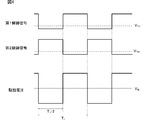
- FIG. 3 is a schematic diagram illustrating waveforms of the first control signal, the second control signal, and the drive voltage according to the first example and the second example of the first embodiment.
- FIG. 4 is a schematic diagram illustrating waveforms of the first control signal, the second control signal, and the drive voltage according to the first comparative example and the second comparative example.
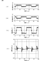
- FIGS. 5A to 5D are diagrams showing waveforms of the first control signal, the second control signal, the drive voltage, and the drive current, respectively, according to the first comparative example.
- FIGS. 5A to 5D are diagrams showing waveforms of the first control signal, the second control signal, the drive voltage, and the drive current, respectively, according to the first comparative example.
- FIGS. 6A to 6D are diagrams showing waveforms of the first control signal, the second control signal, the drive voltage, and the drive current, respectively, according to the second comparative example.
- FIGS. 7A to 7D are diagrams showing waveforms of the first control signal, the second control signal, the drive voltage, and the drive current, respectively, according to the first example of the first embodiment.
- FIGS. 8A to 8D are diagrams showing waveforms of the first control signal, the second control signal, the drive voltage, and the drive current, respectively, according to the second example of the first embodiment.
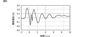
- FIG. 9 is a diagram illustrating ringing of the drive current according to the second example of the first embodiment.
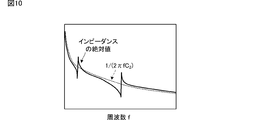
- FIG. 10 is a schematic diagram showing the frequency characteristic of the absolute value of the impedance of the piezoelectric element P.
- FIG. 11 is a diagram illustrating power consumption in the pressure mode according to the first embodiment.
- FIG. 12A is a diagram illustrating the frequency characteristics of the impedance phase in the piezoelectric element P provided in the piezoelectric pump.
- FIG. 12B is a diagram showing the frequency characteristics of the absolute value of impedance in the piezoelectric element P provided in the piezoelectric pump.
- FIG. 13 is a diagram illustrating the frequency characteristics of the absolute value of impedance in the piezoelectric element P provided in the piezoelectric pump.
- FIG. 14A is a diagram showing the vicinity of the fundamental resonance frequency of FIG. FIG.
- FIG. 14B is a diagram showing the vicinity of the 19th resonance frequency of FIG.
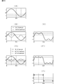
- FIGS. 15A to 15F are diagrams illustrating the Fourier series expansion of a rectangular wave.
- FIG. 16 is a schematic diagram illustrating a waveform of a drive voltage according to the second embodiment.
- FIGS. 17A to 17D are diagrams showing waveforms of the first control signal, the second control signal, the drive voltage, and the drive current, respectively, in the first comparative example.
- FIGS. 18A to 18D are diagrams showing waveforms of the first control signal, the second control signal, the drive voltage, and the drive current, respectively, in the second comparative example.
- FIGS. 19A to 19D are diagrams showing waveforms of the first control signal, the second control signal, the drive voltage, and the drive current, respectively, in the first example of the second embodiment.
- FIGS. 20A to 20D are diagrams showing waveforms of the first control signal, the second control signal, the drive voltage, and the drive current, respectively, in the second example of the second embodiment.
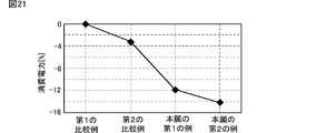
- FIG. 21 is a diagram illustrating power consumption in the flow rate mode according to the second embodiment.
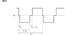
- FIG. 22 is a schematic diagram illustrating a waveform of a drive voltage according to the first example of the third embodiment.
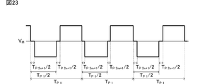
- FIG. 23 is a schematic diagram illustrating a waveform of a drive voltage according to a second example of the third embodiment.
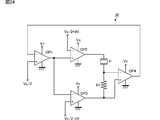
- FIG. 24 is a circuit diagram of the piezoelectric element drive circuit 30 according to the fourth embodiment.
- FIG. 25A and FIG. 25B are schematic diagrams illustrating waveforms of drive voltages according to other embodiments.
- FIG. 1 is a block diagram of a piezoelectric element drive circuit 10 according to a first example of the first embodiment.
- the piezoelectric element drive circuit 10 includes an H-bridge circuit 11 and a control signal generator 12.
- the H-bridge circuit 11 is an example of the “drive voltage generation unit” in the present invention.
- the H bridge circuit 11 has a first input terminal IN1, a second input terminal IN2, a first output terminal OUT1, and a second output terminal OUT2.
- the control signal generator 12 has a first control signal output terminal and a second control signal output terminal.
- the first input terminal IN 1 of the H bridge circuit 11 is connected to the first control signal output terminal of the control signal generator 12.
- the second input terminal IN2 of the H bridge circuit 11 is connected to the second control signal output terminal of the control signal generator 12.
- the first output terminal OUT1 of the H bridge circuit 11 is connected to the first terminal of the piezoelectric element P.
- the second output terminal OUT2 of the H bridge circuit 11 is connected to the second terminal of the piezoelectric element P.
- the absolute value of the impedance of the piezoelectric element P has the highest peak in the 2n + 1 order resonance frequency of the piezoelectric element P among the resonance frequencies of the second or higher order of the piezoelectric element P.
- n is a natural number.
- the peak height is the difference between the value at the peak apex and the value at the peak tail.
- the piezoelectric element P is used for a piezoelectric pump, for example.
- the control signal generator 12 outputs the first control signal from the first control signal output terminal and outputs the second control signal from the second control signal output terminal.
- the frequencies of the first control signal and the second control signal are substantially equal to the basic resonance frequency of the piezoelectric element P.
- the first control signal is input to the first input terminal IN1 of the H bridge circuit 11.
- the second control signal is input to the second input terminal IN2 of the H bridge circuit 11.
- the H bridge circuit 11 drives the piezoelectric element P by changing the states of the first output terminal and the second output terminal in accordance with the first control signal and the second control signal.
- FIG. 2 is a block diagram of the piezoelectric element drive circuit 20 according to the second example of the first embodiment.
- the piezoelectric element drive circuit 20 includes an inductor L1 connected in series between the first output terminal OUT1 of the H-bridge circuit 11 and the first terminal of the piezoelectric element P.
- Other configurations of the piezoelectric element driving circuit 20 are the same as those of the piezoelectric element driving circuit 10.
- the inductor L1 may be connected in series between the second output terminal OUT2 of the H bridge circuit 11 and the second terminal of the piezoelectric element P.
- FIG. 3 is a schematic diagram illustrating waveforms of the first control signal, the second control signal, and the drive voltage according to the first example and the second example of the first embodiment.
- the drive voltage is a potential difference between the first output terminal OUT1 and the second output terminal OUT2 of the H bridge circuit 11.
- V M represents an intermediate potential
- V TH represents a switching threshold.
- the first control signal and the second control signal are rectangular waves having a cycle T 1 and a duty ratio (T 1 + T 2n + 1 ) / 2T 1 .
- time T 2n + 1 T 1 / (2n + 1).
- the phase of the second control signal and the phase of the first control signal are opposite to each other.
- the Hi level potential of the first control signal is equal to the Hi level potential of the first control signal.
- the low level potential of the first control signal is equal to the low level potential of the first control signal.
- the switching threshold of the H bridge circuit 11 is set between the Hi level of the first control signal and the Low level of the first control
- the H-bridge circuit 11 sets the potential of the first output terminal OUT1 to the Hi level and sets the second output terminal The potential of OUT2 is set to a low level. At this time, the drive voltage becomes the maximum value.
- the H-bridge circuit 11 sets the potential of the first output terminal OUT1 to the low level and sets the second output terminal The potential of OUT2 is set to Hi level. At this time, the drive voltage becomes the minimum value.
- the Hi level potential of the first output terminal OUT1 is equal to the Hi level potential of the second output terminal OUT2.
- the low level potential of the first output terminal OUT1 and the low level potential of the second output terminal OUT2 are equal to each other.
- the H bridge circuit 11 sets the first output terminal OUT1 and the second output terminal OUT2 to high impedance when the levels of the first control signal and the second control signal are equal to or higher than the switching threshold.
- the first output terminal OUT1 and the second output terminal OUT2 are in the open state when viewed from the piezoelectric element P side to the H bridge circuit 11 side.
- the drive voltage becomes an intermediate potential. That is, when the drive voltage becomes an intermediate potential, the first output terminal OUT1 and the second output terminal OUT2 are in an open state when viewed from the piezoelectric element P side to the H bridge circuit 11 side.
- the H bridge circuit 11 may set both the potentials of the first output terminal OUT1 and the second output terminal OUT2 to the Hi level or the Low level. . At this time, the drive voltage becomes an intermediate potential. That is, when the driving voltage becomes an intermediate potential, a voltage of 0 V is applied between the first output terminal OUT1 and the second output terminal OUT2.
- the waveform of the drive voltage becomes a step wave. That is, the drive voltage periodically repeats stepwise transitions. In other words, the drive voltage periodically repeats a change due to a steep rise or fall.
- the drive voltage periodically repeats a step-like transition between the maximum value, the minimum value, and the intermediate potential. That is, the waveform of the driving voltage becomes a step wave that transits through an intermediate potential when the piezoelectric element P is driven.
- the intermediate potential of the drive voltage is a potential located between the maximum value (maximum potential) of the drive voltage and the minimum value (minimum potential) of the drive voltage.
- the intermediate potential of the drive voltage is a potential that is equally separated from the maximum value of the drive voltage and the minimum value of the drive voltage, in other words, the median value of the maximum value of the drive voltage and the minimum value of the drive voltage. Determined.
- Cycle of the driving voltage is T 1.
- the time T 1 is substantially equal to the reciprocal of the basic resonance frequency of the piezoelectric element P.
- the amplitude of the drive voltage is twice the potential difference between the maximum potential of the first output terminal OUT1 and the minimum potential of the second output terminal OUT2.
- the time T 2n + 1 is approximately equal to the reciprocal of the 2n + 1 order resonance frequency of the piezoelectric element P.
- the drive voltage pause time is (t 2 -t 1 ) / (2n + 1) from time t 1 to time t 2 .
- FIG. 4 is a schematic diagram illustrating waveforms of the first control signal, the second control signal, and the drive voltage according to the first comparative example and the second comparative example.
- the first control signal and the second control signal are rectangular waves having a cycle T 1 and a duty ratio of 0.5.
- the phase of the second control signal and the phase of the first control signal are opposite to each other.
- the drive voltage is a rectangular wave with a duty ratio of 0.5.
- the period, amplitude, and intermediate potential of the drive voltage are the same as those in the first example and the second example of the first embodiment.
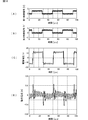
- FIG. 5A to FIG. 5D are diagrams showing waveforms of the first control signal, the second control signal, the drive voltage, and the drive current, respectively, according to the first comparative example.
- the drive current is a current that flows between the first output terminal OUT1 of the H bridge circuit 11 and the second output terminal OUT2 of the H bridge circuit 11.
- the piezoelectric element P is used for a piezoelectric pump, and the piezoelectric pump operates in a pressure mode.
- the pressure mode is a mode in which the piezoelectric pump is operated so that the suction port (or discharge port) of the piezoelectric pump is closed and the pressure of the suction port (or discharge port) of the piezoelectric pump is kept constant.
- sample 1 (see FIG. 11) is used as the piezoelectric pump.
- the frequency of the first control signal, the second control signal, the drive voltage and the drive current is about 23.5 kHz (the period is about 42.6 ⁇ s).
- the amplitude of the first control signal and the second control signal is about 3V.
- the amplitude of the drive voltage is about 24V.
- the drive current instantaneously increases when the drive voltage transitions, in other words, when the drive voltage rises or falls. That is, when the drive voltage transitions, a spike current flows through the first output terminal OUT1. This spike current is due to charging or discharging of the capacitor of the piezoelectric element P.
- a ripple due to the 13th harmonic appears (superimposes) in the drive current.
- the amplitude of this ripple is about 1 ⁇ 2 times the amplitude of the fundamental wave.
- FIG. 6 (A) to 6 (D) are diagrams showing waveforms of the first control signal, the second control signal, the drive voltage, and the drive current, respectively, according to the second comparative example.
- the waveforms of the first control signal, the second control signal, and the drive voltage are the same as those in the first comparative example.
- the drive current when the drive voltage transitions is smaller than that of the first comparative example. This is because the inductor L1 (see FIG. 2) suppresses the high-frequency component of the drive current. In other words, the inductor L1 prevents a steep change in the drive current.
- the amplitude of the drive current ripple is substantially equal to the amplitude of the fundamental wave.
- the amplitude of the ripple of the drive current is larger than that in the case of the first comparative example.
- the resonance frequency of resonance by the inductor L1 and the equivalent capacitor C1 (not shown) of the piezoelectric element P substantially matches the frequency of the 13th harmonic of the drive current.
- the impedance between the first output terminal OUT1 and the second output terminal OUT2 becomes smaller at the frequency of the 13th harmonic of the drive current.
- the amplitude of the 13th harmonic of the drive current is increased, so that the amplitude of the ripple of the drive current is increased as compared with the case of the first comparative example.
- FIGS. 7A to 7D are diagrams showing waveforms of the first control signal, the second control signal, the drive voltage, and the drive current, respectively, according to the first example of the first embodiment.
- the frequency of the first control signal, the second control signal, the drive voltage, and the drive current is about 23.5 kHz (the period is about 42.6 ⁇ s).
- the amplitude of the first control signal and the second control signal is about 3V.
- the amplitude of the drive voltage is about 24V.
- the drive current increases instantaneously every time the drive voltage transitions.
- the drive current when the drive voltage transitions is smaller than that in the first comparative example. This is because the potential difference between the potentials at which the drive voltage transitions once is smaller than in the first comparative example. Further, no ripple appears in the drive current. This pause time of one period per T 1/13 to the drive voltage that is provided, because the 13-order harmonics of the drive current is suppressed. Details regarding this point will be described later.
- FIGS. 8A to 8D are diagrams showing waveforms of the first control signal, the second control signal, the drive voltage, and the drive current, respectively, according to the second example of the first embodiment.
- FIG. 9 is a diagram illustrating ringing of the drive current according to the second example of the first embodiment.
- FIG. 10 is a schematic diagram showing the frequency characteristic of the absolute value of the impedance of the piezoelectric element P. As shown in FIG. In FIG. 9, sample 2 (see FIG. 11) is used as the piezoelectric pump. The vertical axis in FIG. 10 is a logarithmic scale.
- the waveforms of the first control signal, the second control signal, and the driving voltage are the same as those in the first example of the first embodiment.
- the drive current when the drive voltage transitions is smaller than in the second comparative example and the first example of the first embodiment. This is because the high-frequency component of the drive current is suppressed by the inductor L1 (see FIG. 2) as well as the potential difference between the potentials at which the drive voltage transitions once is smaller than in the second comparative example. Further, since the 13th harmonic of the drive current is suppressed, no ripple appears in the drive current.
- the capacitor C ⁇ b> 2 defines a global frequency characteristic of the absolute value of the impedance of the piezoelectric element P. That is, the global frequency characteristic of the absolute value of the impedance of the piezoelectric element P is represented by 1 / (2 ⁇ fC 2 ) where f is the frequency and C 2 is the value of the capacitor C2.
- the capacitor C2 is different from the capacitor C1.
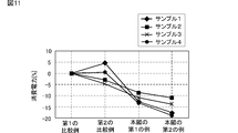
- FIG. 11 is a diagram showing power consumption in the pressure mode according to the first embodiment.
- the power consumption is power consumed when a piezoelectric pump using the piezoelectric element P (see FIG. 1 or FIG. 2) is driven.
- the power consumption is shown as a ratio to the power consumption in the first comparative example.
- FIG. 11 shows the power consumption of four types of piezoelectric pumps.
- the second comparative example there are samples in which the power consumption is reduced compared to the first comparative example, but there are also samples in which the power consumption is increased.
- the power consumption is reduced by about 10% compared to the first comparative example.
- the power consumption is reduced by about 15% although there is some variation depending on the sample as compared with the first comparative example.
- the above spike current and ripple do not contribute to the operation of the piezoelectric pump, but increase the power consumption during the operation of the piezoelectric pump.
- the spike current is suppressed as compared with the first comparative example, but the ripple increases.
- the power consumption of the second comparative example increases from the power consumption of the first comparative example.
- the spike current is somewhat suppressed as compared with the first comparative example, and no ripple appears in the drive current. For this reason, in the 1st example of 1st Embodiment, power consumption decreases compared with the 1st comparative example and the 2nd comparative example.
- the spike current is suppressed as compared with the first example of the first embodiment, and no ripple appears in the drive current.
- the ringing attenuates with time, and thus does not significantly affect power consumption. For this reason, in the second example of the first embodiment, the power consumption is further reduced as compared with the first example of the first embodiment.
- the power reduction effect is not necessarily obtained in all samples as compared to the first comparative example.
- the power reduction effect can be obtained in all samples as compared to the first example of the first embodiment. For this reason, the effect of power reduction in the second example of the first embodiment is a synergistic effect.
- the drive currents of the first comparative example and the first example of the first embodiment are obtained by dividing the drive voltage by the impedance of the piezoelectric element P (see FIG. 1).
- the drive currents of the second comparative example and the second example of the first embodiment are obtained by dividing the drive voltage by the impedance between the first output terminal OUT1 and the second output terminal OUT2 (FIG. 2).
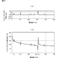
- FIG. 12A is a diagram illustrating the frequency characteristics of the impedance phase in the piezoelectric element P provided in the piezoelectric pump.
- FIG. 12B is a diagram showing the frequency characteristics of the absolute value of impedance in the piezoelectric element P provided in the piezoelectric pump. 12A and 12B, the sample 5 is used as the piezoelectric pump.
- the absolute value of the impedance of the piezoelectric element P has a negative peak due to resonance and a positive peak due to anti-resonance.
- the absolute value of the impedance of the piezoelectric element P is attenuated in inverse proportion to the frequency except in the vicinity of the resonance frequency and the antiresonance frequency.
- the impedance phase of the piezoelectric element P changes sharply at the resonance frequency and the anti-resonance frequency.
- the phase of the impedance of the piezoelectric element P is ⁇ 90 degrees except for the vicinity of the resonance frequency and the antiresonance frequency.
- the basic resonance frequency f A1 of the piezoelectric element P is about 23.5 kHz.
- the absolute value of the impedance of the piezoelectric element P at the basic resonance frequency f A1 is about 200 ⁇ .
- the thirteenth order resonance frequency f A13 of the piezoelectric element P is about 306 kHz.
- the absolute value of the impedance of the piezoelectric element P at the 13th-order resonance frequency f A13 is about 2 ⁇ .
- the absolute value of the impedance of the piezoelectric element P is high in the vicinity of 13 times the basic resonance frequency f A1 of the piezoelectric element P, that is, the 13th-order resonance frequency f A13 among the secondary and higher resonance frequencies of the piezoelectric element P. Has the highest peak.
- the absolute value of the impedance of the piezoelectric element P at the 13th-order resonance frequency f A13 is about 1/100 of the absolute value of the impedance at the basic resonance frequency f A1 .
- the peak height of the absolute value of the impedance of the piezoelectric element P at the 13th-order resonance frequency f A13 is higher than the peak height of the absolute value of the impedance of the piezoelectric element P at the basic resonance frequency f A1 .
- the peak height of the absolute value of the impedance of the piezoelectric element P at the 13th-order resonance frequency f A13 is the highest among the absolute value peaks of the impedance of the piezoelectric element P at the resonance frequency of the piezoelectric element P.
- FIG. 13 is a diagram illustrating the frequency characteristics of the absolute value of impedance in the piezoelectric element P provided in the piezoelectric pump.
- FIG. 14A is a diagram showing the vicinity of the fundamental resonance frequency of FIG.
- FIG. 14B is a diagram showing the vicinity of the 19th resonance frequency of FIG.
- the sample 6 is used as a piezoelectric pump.
- the basic resonance frequency f B1 of the piezoelectric element P is about 20.5 kHz.
- the absolute value of the impedance of the piezoelectric element P at the basic resonance frequency f B1 is about 400 ⁇ .
- the absolute value of the impedance of the piezoelectric element P at the 19th-order resonance frequency f B19 is about 20 ⁇ .
- the absolute value of the impedance at the 19th-order resonance frequency f B19 is about 1/20 of the absolute value of the impedance at the basic resonance frequency f B1 .
- the driving voltage of the first comparative example and the second comparative example is a rectangular wave.
- the rectangular wave g (t) is expressed as shown in Equation (1) and is expanded by Fourier series as shown in Equation (2).
- FIG. 15A shows the waveform of the first-order term of Equation (2).
- FIG. 15B shows the waveforms of the first and second order terms of Equation (2).
- FIG. 15C shows the waveform of the sum of the first and second order terms of Equation (2).
- FIG. 15D shows waveforms of terms from the first order to the third order in the equation (2).
- FIG. 15E shows the waveform of the sum of the terms from the first order to the third order in Equation (2).
- FIG. 15F shows the waveform of the sum of the terms from the first order to the 60th order of Equation (2).
- the cycle T 1.
- the rectangular wave is represented by a superposition of the fundamental wave and the odd-order harmonics.
- the driving voltage includes 2q + 1st order harmonics
- the amplitude of the 2q + 1st order harmonics of the driving voltage is 1 / (2q + 1) of the amplitude of the fundamental wave.
- the frequencies of the first control signal and the second control signal are substantially equal to the basic resonance frequency of the piezoelectric element P.
- the frequency of the drive voltage is substantially equal to the basic resonance frequency of the piezoelectric element P.
- the frequency of the 2q + 1st order harmonic of the drive voltage is substantially equal to the 2q + 1st order resonance frequency of the piezoelectric element P.
- the amplitude of the 2q + 1st harmonic of the drive current is approximately
- Z 1 is the impedance of the piezoelectric element P at the fundamental resonance frequency of the piezoelectric element P.
- Z 2q + 1 is the impedance of the piezoelectric element P at the 2q + 1 order resonance frequency of the piezoelectric element P.
- the amplitude of the 2q + 1st harmonic of the drive current is about the same as the amplitude of the fundamental wave of the drive current. .
- the amplitude of the 2q + 1 order harmonic of the drive current increases as the absolute value
- the absolute value of the impedance of the piezoelectric element P has the highest peak at the 2n + 1-order resonance frequency of the piezoelectric element P among the resonance frequencies of the second or higher order of the piezoelectric element P. .
- the 2n + 1 order harmonic is the main harmonic among the harmonics included in the drive current. Therefore, a ripple due to the 2n + 1 order harmonic appears in the drive current.
- an inductor L1 (see FIG. 2) is provided in the piezoelectric element drive circuit.
- 2n + 1 order harmonics are applied to the drive current on substantially the same principle as in the first comparative example. Ripple due to appears.
- the amplitude of the 2q + 1st harmonic of the drive current is about
- Z S 1 is the impedance between the first output terminal OUT1 and the second output terminal OUT2 at the fundamental resonance frequency of the piezoelectric element P.
- Z S 2q + 1 is the impedance between the first output terminal OUT1 and the second output terminal OUT2 at the 2q + 1 order resonance frequency of the piezoelectric element P.
- the drive voltage is a step wave as shown in FIG.
- the step wave s (t) is expressed as in Expression (3)
- the 2j + 1st order harmonic wave s h (t) included in the step wave s (t) is expressed as Expression (4) by Fourier series expansion.
- the drive voltage does not include 2n + 1 order harmonics.
- the drive current does not include 2n + 1st order harmonics, ripples due to 2n + 1st order harmonics do not appear in the drive current.
- the ripple due to the 2n + 1 order harmonic appears in the drive current, reflecting the frequency characteristics of the impedance of the piezoelectric element P.
- the 2n + 1st order harmonic of the drive current is suppressed, so that the ripple due to the 2n + 1st order harmonic does not appear in the drive current.
- movement of the piezoelectric element P can be reduced compared with the 1st comparative example and the 2nd comparative example.
- an inductor L1 is provided.
- the spike current generated when the drive voltage transitions is suppressed.
- the resonance between the inductor L1 and the equivalent capacitor C1 included in the piezoelectric element P occurs and the impedance between the first output terminal OUT1 and the second output terminal OUT2 is further reduced, the first embodiment.
- 2n + 1 order harmonics of the drive current are suppressed. For this reason, ripples due to 2n + 1 order harmonics do not appear in the drive current.
- useless power consumption can be reduced further.
- the inductor L1 is also provided in the second comparative example, but the power consumption is not necessarily reduced as compared with the first comparative example. For this reason, the effect of the piezoelectric element drive circuit of the second example of the first embodiment is that the drive voltage is a step wave characterized by a pause time T 2n + 1 and that the inductor L1 is provided. This is a synergistic effect.
- Second Embodiment the period in which the drive voltage is the maximum value and the period in which the drive voltage is the minimum value are different per cycle of the drive voltage.
- the first example of the second embodiment has the same circuit configuration as that of the first example of the first embodiment (see FIG. 1).
- the second example of the second embodiment has a circuit configuration similar to that of the second example of the first embodiment (see FIG. 2).
- FIG. 16 is a schematic diagram illustrating waveforms of drive voltages according to the first example and the second example of the second embodiment.
- Cycle of the driving voltage is T 1.
- Drive voltage during the time T 2n + 1/2 becomes an intermediate potential, during the next time T A -T 2n + 1/2 , is the minimum value, during the next time T 2n + 1/2, It becomes an intermediate potential and becomes the maximum value during the next T 1 ⁇ T A ⁇ T 2n + 1/2 .
- the drive voltage periodically repeats this step-like transition.
- Time T A has a value different from time T 1/2 .
- FIGS. 17A to 17D are diagrams showing waveforms of the first control signal, the second control signal, the drive voltage, and the drive current, respectively, in the first comparative example.
- the piezoelectric element P is used for a piezoelectric pump, and the piezoelectric pump operates in a flow rate mode.
- the flow rate mode is a mode in which the piezoelectric pump is operated so that the suction port and discharge port of the piezoelectric pump are opened and the flow rate of the suction port or discharge port of the piezoelectric pump is constant.
- the sample 1 (see FIG. 11) is used as the piezoelectric pump. These points are the same in FIGS.
- FIGS. 18A to 18D FIGS. 19A to 19D, and FIGS. 20A to 20D.
- the waveforms of the first control signal, the second control signal, the drive voltage, and the drive current are the same as those in the pressure mode (see FIGS. 5A to 5D).
- FIGS. 18A to 18D are diagrams showing waveforms of the first control signal, the second control signal, the drive voltage, and the drive current, respectively, in the second comparative example.
- the waveforms of the first control signal, the second control signal, the drive voltage, and the drive current are the same as those in the pressure mode (see FIGS. 6A to 6D).
- FIGS. 19A to 19D are diagrams showing waveforms of the first control signal, the second control signal, the drive voltage, and the drive current, respectively, in the first example of the second embodiment.
- the frequency of the first control signal, the second control signal, the drive voltage, and the drive current is about 23.5 kHz (the period is about 42.6 ⁇ s).
- the amplitude of the first control signal and the second control signal is about 3V.
- the amplitude of the drive voltage is about 24V.
- the drive current increases instantaneously every time the drive voltage transitions.
- the drive current when the drive voltage transitions is smaller than that in the first comparative example. Further, no ripple appears in the drive current.
- 20A to 20D are diagrams showing waveforms of the first control signal, the second control signal, the drive voltage, and the drive current, respectively, in the second example of the second embodiment.
- the waveforms of the first control signal, the second control signal, and the drive voltage are the same as those in the first example of the second embodiment.
- the drive current when the drive voltage transitions is smaller than in the second comparative example and the first example of the first embodiment. No ripple appears in the drive current. On the other hand, ringing that attenuates and oscillates from the time when the drive voltage transitions appears in the drive current.
- FIG. 21 is a diagram showing power consumption in the flow rate mode according to the second embodiment.
- the power consumption is shown as a ratio to the power consumption in the first comparative example.
- Sample 1 (see FIG. 11) is used as the piezoelectric pump.
- power consumption is reduced by about 3%.
- power consumption is reduced by about 12%.
- the power consumption is reduced by about 15%.
- an effect equivalent to that of the first example of the first embodiment is obtained.
- an effect equivalent to that of the second example of the first embodiment can be obtained.
- FIG. 22 is a schematic diagram illustrating a waveform of a drive voltage according to the first example of the third embodiment.
- Cycle of the driving voltage is T 1.
- Drive voltage during the time T B becomes the intermediate potential, during the next time T 1/2-T B, becomes the minimum value, during the next time T 2n + 1 -T B, becomes the intermediate potential, the following The maximum value is obtained during T 1 / 2 ⁇ (T 2n + 1 ⁇ T B ).
- the drive voltage periodically repeats this step-like transition.
- Time T B has a time T 2n + 1/2 and different values.
- the drive voltage pause time varies for each time length T P1 .
- the time length T P1 is the time from when the drive voltage falls to the intermediate potential until the next time when the drive voltage falls to the intermediate potential, and is approximately equal to the reciprocal of the basic resonance frequency of the piezoelectric element P.
- FIG. 23 is a schematic diagram illustrating a waveform of a drive voltage according to a second example of the third embodiment. The period of the driving voltage is 2T P1 .
- T P 2n + 1/2 becomes an intermediate potential, during the next time (T P1 -T P 2n + 1 ) / 2, is the minimum value, the next time T P 2n + 1 The potential becomes intermediate during / 2, and the maximum value during the next (T P1 -T P 2n + 1 ) / 2.
- Driving voltage during the next time T P 2m + 1/2 becomes an intermediate potential, during the next time (T P1 -T P 2m + 1 ) / 2, is the minimum value, the next time T P 2m between +1 / 2 becomes the intermediate potential, during the next (T P1 -T P 2m + 1 ) / 2, it becomes a maximum value.
- the drive voltage periodically repeats this step-like transition.
- T P 2n + 1 T P1 / (2n + 1)
- T P 2m + 1 T P1 / (2m + 1).
- n and m are natural numbers, and n and m are different from each other.
- the drive voltage pause time is defined by two odd numbers 2n + 1, 2m + 1 .
- the drive voltage pause time is specified by two or more odd numbers. Or may be arbitrarily changed.
- the absolute value of the impedance of the piezoelectric element P has a plurality of large peaks (strong response), it is preferable that the drive voltage pause time differs for each time length T P1 .
- FIG. 24 is a circuit diagram of the piezoelectric element drive circuit 30 according to the fourth embodiment.
- the piezoelectric element drive circuit 30 includes operational amplifiers OP1 to OP4 and a resistor R1.
- the circuit composed of the operational amplifiers OP1 to OP3 is an example of the “drive voltage generation unit” in the present invention.
- a reference voltage Vc / 2 is applied to the positive phase input terminal of the operational amplifier OP1.
- the negative phase input terminal of the operational amplifier OP1 is connected to the output terminal of the operational amplifier OP4.
- the output terminal of the operational amplifier OP1 is connected to the positive phase input terminal of the operational amplifier OP2 and the negative phase input terminal of the operational amplifier OP3.
- a reference voltage Vc / 2 + dV is applied to the negative phase input terminal of the operational amplifier OP2.
- the output terminal of the operational amplifier OP2 is connected to the first terminal of the piezoelectric element P.
- a reference voltage Vc / 2-dV is applied to the positive phase input terminal of the operational amplifier OP3.
- the output terminal of the operational amplifier OP3 is connected to the second terminal of the piezoelectric element P through the resistor R1.
- the positive phase input terminal and the negative phase input terminal of the operational amplifier OP4 are connected to the first terminal and the second terminal of the resistor R1, respectively.
- Vc is applied to the positive power supply terminals of the operational amplifiers OP1 to OP4.
- the negative power supply terminals of the operational amplifiers OP1 to OP4 are grounded.
- the characteristics of each circuit element of the piezoelectric element drive circuit 30 are determined so as to satisfy Barkhausen's oscillation condition at the fundamental resonance frequency of the piezoelectric element P. Therefore, the piezoelectric element drive circuit 30 drives the piezoelectric element P at the basic resonance frequency of the piezoelectric element P.
- the operational amplifier OP4 detects a voltage proportional to the drive current and differentially amplifies the voltage.
- the operational amplifier OP1 amplifies the difference between the output signal of the operational amplifier OP1 and the reference voltage Vc / 2.
- the operational amplifier OP1 is an inverting amplifier circuit.
- the output signal of the operational amplifier OP1 is a substantially trapezoidal wave.
- the operational amplifier OP2 amplifies the difference between the output signal of the operational amplifier OP1 and the reference voltage Vc / 2 + dV.
- the operational amplifier OP2 is a non-inverting amplifier circuit.
- the operational amplifier OP3 amplifies the difference between the output signal of the operational amplifier OP1 and the reference voltage Vc / 2 ⁇ dV.
- the operational amplifier OP3 is an inverting amplifier circuit.
- the intermediate potential of the drive voltage is set to the median value of the maximum value of the drive voltage and the minimum value of the drive voltage.
- the intermediate potential is set to the minimum value from the median value. It may be set to a close value or a value closer to the maximum value than the median value.
- waveform of the driving voltage intermediate potential V M takes a value close to the minimum value than the median V 0 is shown.
- Figure 25 (B) shows a waveform of a driving voltage to the intermediate voltage V M takes a value close to the maximum value than the median V 0 is shown.
- the potential at which the drive voltage transitions is between the maximum value and the minimum value.
- the potential at which the drive voltage transitions is between the maximum value and the minimum value.
- the drive voltage may transition to a maximum value, a minimum value, and a plurality of intermediate potentials.
- an inductor is provided, but another element or circuit that can remove a high-frequency component of the drive current may be provided.
- the odd number 2n + 1 that defines the drive voltage is determined from the peak of the absolute value of the impedance of the piezoelectric element having the highest peak.
- the odd number 2n + 1 is the piezoelectric element. May be determined from another peak of the absolute value of the impedance.
Landscapes
- Engineering & Computer Science (AREA)
- Mechanical Engineering (AREA)
- General Engineering & Computer Science (AREA)
- Computer Hardware Design (AREA)
- General Electrical Machinery Utilizing Piezoelectricity, Electrostriction Or Magnetostriction (AREA)
Abstract
圧電素子用駆動回路は、所定の周波数で駆動し、該所定の周波数の(2n+1)倍の共振周波数(nは所定の自然数)を有した圧電素子と、圧電素子の第1端子に接続される第1出力端子、および、圧電素子の第2端子に接続される第2出力端子を有する駆動電圧生成部を備える。圧電素子が駆動されるとき、第1出力端子と第2出力端子との間の電位差の波形は、中間電位を経て遷移するステップ波となる。前記電位差が中間電位となる時間の長さは、前記電位差が中間電位に立ち下がる時間t1から次に前記電位差が中間電位に立ち下がる時間t2までの間において、(t2-t1)/(2n+1)付近である。
Description
本発明は、圧電素子を駆動する圧電素子用駆動回路に関する。
従来の圧電素子用駆動回路として、例えば、特許文献1に記載のものがある。この圧電素子用駆動回路は、Hブリッジ回路、抵抗器、差動増幅回路、反転回路、第1コンパレータおよび第2コンパレータを備える。Hブリッジ回路は、第1入力端子および第2入力端子と、圧電素子の両端子にそれぞれ接続される第1出力端子および第2出力端子とを有する。抵抗器は圧電素子とHブリッジ回路の第1出力端子との間に接続される。差動増幅回路は抵抗器の両端電圧を入力とする。反転回路の入力端子は差動増幅回路の出力端子に接続される。第1コンパレータの入力端子は反転回路の入力端子に接続される。第1コンパレータの出力端子はHブリッジ回路の第1入力端子に接続される。第2コンパレータの入力端子は反転回路の出力端子に接続される。第2コンパレータの出力端子はHブリッジ回路の第2入力端子に接続される。
特許文献1に記載の圧電素子用駆動回路では、駆動電圧が矩形波であることで駆動電圧が低くなるので、圧電素子の動作時の消費電力が低減される。一方、矩形波からなる駆動電圧には、圧電素子の実質的な動作に寄与せず、電力を消費するだけの高調波が含まれる。このため、この圧電素子用駆動回路では、駆動電圧が矩形波であること以外の他の要因次第で、消費電力が十分低減されないおそれがある。
本発明の目的は、圧電素子の実質的な動作に寄与しない無駄な消費電力を低減できる圧電素子用駆動回路を提供することにある。
本発明の圧電素子用駆動回路は、所定の周波数で駆動し、該所定の周波数の(2n+1)倍の共振周波数(nは所定の自然数)を有した圧電素子と、前記圧電素子の第1端子に接続される第1出力端子、および、前記圧電素子の第2端子に接続される第2出力端子を有する駆動電圧生成部を備える。前記圧電素子が駆動されるとき、前記第1出力端子と前記第2出力端子との間の電位差の波形は、中間電位を経て遷移するステップ波となる。前記電位差が前記中間電位となる時間の長さは、前記電位差が前記中間電位に立ち下がる時間t1から次に前記電位差が前記中間電位に立ち下がる時間t2までの間において、(t2-t1)/(2n+1)付近である。
上記のような圧電素子を駆動する場合、第1出力端子と第2出力端子との間に流れる駆動電流には、2n+1次高調波によるリップルが現れることがある。上記の構成では、駆動電流の2n+1次高調波が抑制されるので、駆動電流に2n+1次高調波によるリップルが発生しにくい。このため、駆動電流に2n+1次高調波によるリップルが現れる場合に比べて、圧電素子の実質的な動作に寄与しない無駄な消費電力を低減できる。
前記所定の周波数の(2n+1)倍の共振周波数における前記圧電素子のインピーダンスの絶対値のピークの高さが、前記所定の周波数における前記圧電素子のインピーダンスの絶対値のピークの高さより高くてもよい。この構成では、圧電素子の実質的な動作に寄与しない無駄な消費電力の低減効果がより高まる。
前記所定の周波数の(2n+1)倍の共振周波数における前記圧電素子のインピーダンスの絶対値のピークの高さが、前記圧電素子の共振周波数における前記圧電素子のインピーダンスの絶対値のピークの中で、最も高くてもよい。この構成では、圧電素子の実質的な動作に寄与しない無駄な消費電力の低減効果がさらに高まる。
本発明の圧電素子用駆動回路は次のように構成されてもよい。第1制御信号出力端子および第2制御信号出力端子を有する制御信号発生部を備える。前記駆動電圧生成部は、前記第1制御信号出力端子に接続される第1入力端子、および、前記第2制御信号出力端子に接続される第2入力端子を有する。
本発明の圧電素子用駆動回路は、前記第1出力端子と前記圧電素子の第1端子との間に直列接続されるインダクタを備えてもよい。この構成では、第1出力端子と第2出力端子との間の電位差(駆動電圧)が遷移するときに発生するスパイク状の駆動電流が抑制される。このため、圧電素子の実質的な動作に寄与しない無駄な消費電力を低減できる。
前記電位差が前記中間電位となるとき、前記圧電素子側から前記駆動電圧生成部側を見て、前記第1出力端子および前記第2出力端子は開放状態でもよい。
前記電位差が前記中間電位となるとき、前記第1出力端子と前記第2出力端子との間に電圧0Vが印加されてもよい。
本発明によれば、圧電素子の実質的な動作に寄与しない無駄な消費電力を低減できる。
以降、図を参照して幾つかの具体的な例を挙げて、本発明を実施するための複数の形態を示す。各図中には同一箇所に同一符号を付している。要点の説明または理解の容易性を考慮して、便宜上実施形態を分けて示すが、異なる実施形態で示した構成の部分的な置換または組み合わせが可能である。第2の実施形態以降では第1の実施形態と共通の事柄についての記述を省略し、異なる点についてのみ説明する。特に、同様の構成による同様の作用効果については実施形態毎には逐次言及しない。
《第1の実施形態》
図1は、第1の実施形態の第1の例に係る圧電素子用駆動回路10のブロック図である。圧電素子用駆動回路10はHブリッジ回路11および制御信号発生部12を備える。Hブリッジ回路11は本発明の「駆動電圧生成部」の一例である。Hブリッジ回路11は、第1入力端子IN1、第2入力端子IN2、第1出力端子OUT1および第2出力端子OUT2を有する。制御信号発生部12は第1制御信号出力端子および第2制御信号出力端子を有する。Hブリッジ回路11の第1入力端子IN1は制御信号発生部12の第1制御信号出力端子に接続される。Hブリッジ回路11の第2入力端子IN2は制御信号発生部12の第2制御信号出力端子に接続される。Hブリッジ回路11の第1出力端子OUT1は圧電素子Pの第1端子に接続される。Hブリッジ回路11の第2出力端子OUT2は圧電素子Pの第2端子に接続される。圧電素子Pのインピーダンスの絶対値は、圧電素子Pの2次以上の共振周波数の中で、圧電素子Pの2n+1次の共振周波数において、高さが最も高いピークを有する。ここで、nは自然数である。ピークの高さは、ピークの頂点における値とピークの裾における値との差分である。圧電素子Pは、例えば圧電ポンプに用いられるものである。
図1は、第1の実施形態の第1の例に係る圧電素子用駆動回路10のブロック図である。圧電素子用駆動回路10はHブリッジ回路11および制御信号発生部12を備える。Hブリッジ回路11は本発明の「駆動電圧生成部」の一例である。Hブリッジ回路11は、第1入力端子IN1、第2入力端子IN2、第1出力端子OUT1および第2出力端子OUT2を有する。制御信号発生部12は第1制御信号出力端子および第2制御信号出力端子を有する。Hブリッジ回路11の第1入力端子IN1は制御信号発生部12の第1制御信号出力端子に接続される。Hブリッジ回路11の第2入力端子IN2は制御信号発生部12の第2制御信号出力端子に接続される。Hブリッジ回路11の第1出力端子OUT1は圧電素子Pの第1端子に接続される。Hブリッジ回路11の第2出力端子OUT2は圧電素子Pの第2端子に接続される。圧電素子Pのインピーダンスの絶対値は、圧電素子Pの2次以上の共振周波数の中で、圧電素子Pの2n+1次の共振周波数において、高さが最も高いピークを有する。ここで、nは自然数である。ピークの高さは、ピークの頂点における値とピークの裾における値との差分である。圧電素子Pは、例えば圧電ポンプに用いられるものである。
制御信号発生部12は、第1制御信号出力端子から第1制御信号を出力するとともに、第2制御信号出力端子から第2制御信号を出力する。第1制御信号および第2制御信号の周波数は圧電素子Pの基本共振周波数と略等しい。第1制御信号はHブリッジ回路11の第1入力端子IN1に入力される。第2制御信号はHブリッジ回路11の第2入力端子IN2に入力される。Hブリッジ回路11は、第1制御信号および第2制御信号に応じて、第1出力端子および第2出力端子の状態を変化させることで、圧電素子Pを駆動する。
図2は、第1の実施形態の第2の例に係る圧電素子用駆動回路20のブロック図である。圧電素子用駆動回路20は、Hブリッジ回路11の第1出力端子OUT1と圧電素子Pの第1端子との間に直列接続されるインダクタL1を備える。圧電素子用駆動回路20のその他の構成は圧電素子用駆動回路10と同様である。なお、インダクタL1は、Hブリッジ回路11の第2出力端子OUT2と圧電素子Pの第2端子との間に直列接続されてもよい。
図3は、第1の実施形態の第1の例および第2の例に係る、第1制御信号、第2制御信号、および、駆動電圧の波形を示す模式図である。駆動電圧は、Hブリッジ回路11の第1出力端子OUT1と第2出力端子OUT2との間の電位差である。VMは中間電位を表し、VTHはスイッチング閾値を表す。第1制御信号および第2制御信号は、周期T1およびデューティー比(T1+T2n+1)/2T1の矩形波である。ここで、時間T2n+1=T1/(2n+1)である。第2制御信号の位相と第1制御信号の位相とは互いに逆相である。第1制御信号のHiレベルの電位と第1制御信号のHiレベルの電位とは互いに等しい。第1制御信号のLowレベルの電位と第1制御信号のLowレベルの電位とは互いに等しい。Hブリッジ回路11のスイッチング閾値は第1制御信号のHiレベルと第1制御信号のLowレベルとの間に設定される。
Hブリッジ回路11は、第1制御信号の電位がスイッチング閾値以上であり、且つ、第2制御信号の電位がスイッチング閾値未満の場合、第1出力端子OUT1の電位をHiレベルにし、第2出力端子OUT2の電位をLowレベルにする。このとき、駆動電圧は最大値となる。Hブリッジ回路11は、第1制御信号の電位がスイッチング閾値未満であり、且つ、第2制御信号の電位がスイッチング閾値以上の場合、第1出力端子OUT1の電位をLowレベルにし、第2出力端子OUT2の電位をHiレベルにする。このとき、駆動電圧は最小値となる。ここで、第1出力端子OUT1のHiレベルの電位と第2出力端子OUT2のHiレベルの電位とは互いに等しい。第1出力端子OUT1のLowレベルの電位と第2出力端子OUT2のLowレベルの電位とは互いに等しい。
Hブリッジ回路11は、第1制御信号および第2制御信号のレベルがスイッチング閾値以上の場合、第1出力端子OUT1および第2出力端子OUT2をハイインピーダンスにする。換言すると、第1制御信号および第2制御信号の電位がスイッチング閾値以上の場合、圧電素子P側からHブリッジ回路11側を見て、第1出力端子OUT1および第2出力端子OUT2が開放状態となる。このとき、駆動電圧は中間電位となる。即ち、駆動電圧が中間電位となるとき、圧電素子P側からHブリッジ回路11側を見て、第1出力端子OUT1および第2出力端子OUT2は開放状態である。
または、Hブリッジ回路11は、第1制御信号および第2制御信号の電位がスイッチング閾値以上の場合、第1出力端子OUT1および第2出力端子OUT2の電位を共にHiレベルまたはLowレベルにしてもよい。このとき、駆動電圧は中間電位となる。即ち、駆動電圧が中間電位となるとき、第1出力端子OUT1および第2出力端子OUT2との間に電圧0Vが印加される。
Hブリッジ回路11が上記のように動作するので、駆動電圧の波形はステップ波となる。即ち、駆動電圧は階段状の遷移を周期的に繰返す。換言すると、駆動電圧は急峻な立ち上がりまたは立ち下がりによる変化を周期的に繰返す。駆動電圧は、最大値、最小値および中間電位の間の階段状の遷移を周期的に繰返す。即ち、駆動電圧の波形は、圧電素子Pが駆動されるとき、中間電位を経て遷移するステップ波となる。駆動電圧の中間電位は、駆動電圧の最大値(最大電位)と駆動電圧の最小値(最小電位)との間に位置する電位である。第1の実施形態において、駆動電圧の中間電位は、駆動電圧の最大値と駆動電圧の最小値とから等しく離れた電位、換言すると、駆動電圧の最大値と駆動電圧の最小値の中央値に定められる。駆動電圧の周期はT1である。時間T1は圧電素子Pの基本共振周波数の逆数に略等しい。駆動電圧の振幅は、第1出力端子OUT1の最大値の電位と第2出力端子OUT2の最小値の電位との間の電位差の2倍である。
駆動電圧が中間電位となる時間の長さ(休止時間)は、1周期当り、T2n+1=T1/(2n+1)である。時間T2n+1は圧電素子Pの2n+1次の共振周波数の逆数に略等しい。駆動電圧は、時間t1に最大値から中間電位に立ち下がり、次に時間t2=t1+T1に最大値から中間電位に立ち下がる。駆動電圧の休止時間は、時間t1から時間t2までの間において、(t2-t1)/(2n+1)である。駆動電圧は、時間T2n+1/2の間、中間電位となり、次の時間(T1-T2n+1)/2の間、最小値となり、次の時間T2n+1/2の間、中間電位となり、次の時間(T1-T2n+1)/2の間、最大値となる。駆動電圧はこの階段状の遷移を周期的に繰返す。
次に、第1の比較例の圧電素子用駆動回路について説明する。第1の比較例の圧電素子用駆動回路は、圧電素子用駆動回路10(図1参照)と同様に構成される。第2の比較例の圧電素子用駆動回路は、圧電素子用駆動回路20(図2参照)と同様に構成される。図4は、第1の比較例および第2の比較例に係る、第1制御信号、第2制御信号および駆動電圧の波形を示す模式図である。第1制御信号および第2制御信号は、周期T1およびデューティー比0.5の矩形波である。第2制御信号の位相と第1制御信号の位相とは互いに逆相である。駆動電圧はデューティー比0.5の矩形波である。第1の比較例および第2の比較例において、駆動電圧の周期、振幅および中間電位は、第1の実施形態の第1の例および第2の例の場合と同様である。
図5(A)から図5(D)は、それぞれ、第1の比較例に係る、第1制御信号、第2制御信号、駆動電圧および駆動電流の波形を示す図である。駆動電流は、Hブリッジ回路11の第1出力端子OUT1とHブリッジ回路11の第2出力端子OUT2との間を流れる電流である。図5(A)から図5(D)では、圧電素子Pが圧電ポンプに用いられ、その圧電ポンプが圧力モードで動作している。圧力モードは、圧電ポンプの吸引口(または吐出口)を閉塞状態にし、圧電ポンプの吸引口(または吐出口)の圧力を一定にするように圧電ポンプを動作させるモードである。図5(A)から図5(D)では、圧電ポンプとして、サンプル1(図11参照)が用いられている。これらの点は、図6(A)から図6(D)、図7(A)から図7(D)および図8(A)から図8(D)でも同様である。
第1制御信号、第2制御信号、駆動電圧および駆動電流の周波数は約23.5kHzである(周期は約42.6μsである)。第1制御信号および第2制御信号の振幅は約3Vである。駆動電圧の振幅は約24Vである。駆動電流は、駆動電圧が遷移する時に、換言すると、駆動電圧の立ち上がりまたは立ち下がり時に、瞬間的に増大する。即ち、駆動電圧が遷移する時に、第1出力端子OUT1にスパイク電流が流れる。このスパイク電流は、圧電素子Pが有するキャパシタの充電または放電によるものである。駆動電流には13次高調波によるリップルが現れる(重畳される)。このリップルの振幅は基本波の振幅の約1/2倍である。
図6(A)から図6(D)は、それぞれ、第2の比較例に係る、第1制御信号、第2制御信号、駆動電圧および駆動電流の波形を示す図である。第1制御信号、第2制御信号および駆動電圧の波形は第1の比較例の場合と同様である。駆動電圧が遷移する時の駆動電流は、第1の比較例の場合に比べて小さい。これは、インダクタL1(図2参照)により駆動電流の高周波成分が抑制されるため、換言すると、インダクタL1により駆動電流の急峻な変化が妨げられるためである。駆動電流のリップルの振幅は基本波の振幅と略等しい。駆動電流のリップルの振幅は第1の比較例の場合に比べて大きい。
インダクタL1と圧電素子Pが有する等価的なキャパシタC1(図示せず)とによる共振の共振周波数は、駆動電流の13次高調波の周波数と略一致する。これにより、第1の比較例の場合に比べて、駆動電流の13次高調波の周波数において第1出力端子OUT1と第2出力端子OUT2との間のインピーダンスが小さくなる。その結果、駆動電流の13次高調波の振幅が大きくなるので、駆動電流のリップルの振幅が第1の比較例の場合に比べて大きくなる。
図7(A)から図7(D)は、それぞれ、第1の実施形態の第1の例に係る、第1制御信号、第2制御信号、駆動電圧および駆動電流の波形を示す図である。第1制御信号、第2制御信号、駆動電圧および駆動電流の周波数は約23.5kHzである(周期は約42.6μsである)。第1制御信号および第2制御信号の振幅は約3Vである。駆動電圧の振幅は約24Vである。第1制御信号、第2制御信号および駆動電圧において、n=6、即ち、T2n+1=T13=T1/13である(図3参照)。
駆動電流は、駆動電圧が遷移する度に、瞬間的に増大する。駆動電圧が遷移するときの駆動電流は、第1の比較例の場合より小さい。これは、駆動電圧が1度に遷移する電位間の電位差が第1の比較例の場合より小さいからである。また、駆動電流にはリップルが現れない。これは、駆動電圧に1周期当りT1/13の休止時間が設けられることで、駆動電流に含まれる13次高調波が抑制されるためである。この点に関する詳細については後述する。
図8(A)から図8(D)は、それぞれ、第1の実施形態の第2の例に係る、第1制御信号、第2制御信号、駆動電圧および駆動電流の波形を示す図である。図9は、第1の実施形態の第2の例に係る駆動電流のリンギングを示す図である。図10は、圧電素子Pのインピーダンスの絶対値の周波数特性を示す模式図である。図9では、圧電ポンプとしてサンプル2(図11参照)が用いられている。図10の縦軸は対数目盛である。
第1制御信号、第2制御信号および駆動電圧の波形は第1の実施形態の第1の例の場合と同様である。駆動電圧が遷移するときの駆動電流は、第2の比較例および第1の実施形態の第1の例の場合に比べて小さい。これは、駆動電圧が1度に遷移する電位間の電位差が第2比較例の場合より小さいことと共に、インダクタL1(図2参照)により駆動電流の高周波成分が抑制されるためである。また、駆動電流の13次高調波が抑制されるので、駆動電流にはリップルが現れない。
一方、駆動電流には、インダクタL1と圧電素子Pが有する等価的なキャパシタC2(図示せず)とによる共振が生じることで、駆動電圧が遷移した時から減衰振動するリンギングが現れる。駆動電流のリンギングの周波数は約490kHzである。図10に示すように、キャパシタC2は圧電素子Pのインピーダンスの絶対値の大域的な周波数特性を定めている。即ち、圧電素子Pのインピーダンスの絶対値の大域的な周波数特性は、周波数をfとし、キャパシタC2の値をC2として、1/(2πfC2)で表される。なお、キャパシタC2は上記のキャパシタC1と異なるものである。
図11は、第1の実施形態に係る、圧力モードにおける消費電力を示す図である。ここで、消費電力は、圧電素子P(図1または図2参照)を用いた圧電ポンプを駆動させたときに消費される電力である。図11では、第1の比較例における消費電力に対する比率で消費電力が示されている。図11では、4種類の圧電ポンプの消費電力が示されている。第2の比較例では、第1の比較例に比べて、消費電力が削減されたサンプルもあるが、消費電力が増加したサンプルもある。第1の実施形態の第1の例では、第1の比較例に比べて、消費電力が約10%削減される。第1の実施形態の第2の例では、第1の比較例に比べて、サンプルにより幾分ばらつきがあるが、消費電力が約15%削減される。
上記のスパイク電流およびリップルは、圧電ポンプの動作に寄与しないが、圧電ポンプの動作時の消費電力を増加させる。第2の比較例では、第1の比較例と比べて、スパイク電流が抑制されるが、リップルが増大する。このため、第2の比較例では、第1の比較例と比べて、消費電力が増加するサンプルと消費電力が減少するサンプルがある。サンプル1では、消費電力に対してリップルの増大の影響がスパイク電流の減少の影響より大きいので、第2の比較例の消費電力が第1の比較例の消費電力より増加する。
第1の実施形態の第1の例では、第1の比較例と比べてスパイク電流が多少抑制されるとともに、駆動電流にリップルが現れない。このため、第1の実施形態の第1の例では、第1の比較例および第2の比較例と比べて、消費電力が減少する。第1の実施形態の第2の例では、第1の実施形態の第1の例と比べてスパイク電流が抑制されるとともに、駆動電流にリップルが現れない。また、リンギングは、時間の経過とともに減衰するので、消費電力に対してあまり影響を与えない。このため、第1の実施形態の第2の例では、第1の実施形態の第1の例と比べて、さらに消費電力が減少する。第2の比較例では、第1の比較例と比べて、必ずしも全てのサンプルで電力削減の効果が得られるわけではない。第1の実施形態の第2の例では、第1の実施形態の第1の例に比べて、全てのサンプルで電力削減の効果が得られる。このため、第1の実施形態の第2の例の電力削減の効果は相乗効果である。
次に、第1の比較例および第2の比較例において駆動電流にリップルが現れるが、第1の実施形態の第1の例および第2の例において駆動電流にリップルが現れない理由について説明する。第1の比較例および第1の実施形態の第1の例の駆動電流は、駆動電圧を圧電素子Pのインピーダンスで除算することで得られる(図1参照)。第2の比較例および第1の実施形態の第2の例の駆動電流は、駆動電圧を、第1出力端子OUT1と第2出力端子OUT2との間のインピーダンスで除算することで得られる(図2参照)。
図12(A)は、圧電ポンプに設けられた圧電素子Pにおけるインピーダンスの位相の周波数特性を示す図である。図12(B)は、圧電ポンプに設けられた圧電素子Pにおけるインピーダンスの絶対値の周波数特性を示す図である。図12(A)および図12(B)では、圧電ポンプとしてサンプル5が用いられている。圧電素子Pのインピーダンスの絶対値は、共振による負方向のピークおよび反共振による正方向のピークを有する。圧電素子Pのインピーダンスの絶対値は、共振周波数および反共振周波数付近を除いて、周波数に反比例して減衰する。圧電素子Pのインピーダンスの位相は、共振周波数および反共振周波数において急峻に変化する。圧電素子Pのインピーダンスの位相は、共振周波数および反共振周波数付近を除いて、-90度である。圧電素子Pの基本共振周波数fA1は約23.5kHzである。基本共振周波数fA1における圧電素子Pのインピーダンスの絶対値は約200Ωである。圧電素子Pの13次の共振周波数fA13は約306kHzである。13次の共振周波数fA13における圧電素子Pのインピーダンスの絶対値は約2Ωである。圧電素子Pのインピーダンスの絶対値は、圧電素子Pの2次以上の共振周波数の中で、圧電素子Pの基本共振周波数fA1の13倍付近、即ち、13次の共振周波数fA13に、高さが最も高いピークを有する。13次の共振周波数fA13における圧電素子Pのインピーダンスの絶対値は、基本共振周波数fA1におけるインピーダンスの絶対値の約1/100である。13次の共振周波数fA13における圧電素子Pのインピーダンスの絶対値のピークの高さは、基本共振周波数fA1における圧電素子Pのインピーダンスの絶対値のピークの高さより高い。13次の共振周波数fA13における圧電素子Pのインピーダンスの絶対値のピークの高さは、圧電素子Pの共振周波数における圧電素子Pのインピーダンスの絶対値のピークの中で、最も高い。
図13は、圧電ポンプに設けられた圧電素子Pにおけるインピーダンスの絶対値の周波数特性を示す図である。図14(A)は、図13(A)の基本共振周波数付近を示す図である。図14(B)は、図13(A)の第19次の共振周波数付近を示す図である。図13では、圧電ポンプとしてサンプル6が用いられている。圧電素子Pの基本共振周波数fB1は約20.5kHzである。基本共振周波数fB1における圧電素子Pのインピーダンスの絶対値は約400Ωである。19次の共振周波数fB19における圧電素子Pのインピーダンスの絶対値は約20Ωである。19次の共振周波数fB19におけるインピーダンスの絶対値は、基本共振周波数fB1におけるインピーダンスの絶対値の約1/20である。
第1の比較例および第2の比較例の駆動電圧は矩形波である。矩形波g(t)は、式(1)のように示され、式(2)のようにフーリエ級数展開される。

ここで、kは整数であり、Tは周期であり、ω=2π/Tは角周波数である。図15(A)は式(2)の1次の項の波形を示す。図15(B)は式(2)の1次および2次の項の波形を示す。図15(C)は式(2)の1次および2次の項の和の波形を示す。図15(D)は式(2)の1次から3次までの項の波形を示す。図15(E)は式(2)の1次から3次までの項の和の波形を示す。図15(F)は式(2)の1次から60次までの項の和の波形を示す。図15(A)から図15(F)では周期T=1としている。このように、矩形波は基本波および奇数次の高調波の重ね合わせで表される。
第1の比較例および第2の比較例において、qを自然数として、駆動電圧は2q+1次高調波を含み、駆動電圧の2q+1次高調波の振幅は基本波の振幅の1/(2q+1)である。また、上記のように、第1制御信号および第2制御信号の周波数は圧電素子Pの基本共振周波数と略等しい。このため、駆動電圧の周波数は圧電素子Pの基本共振周波数と略等しい。駆動電圧の2q+1次高調波の周波数は圧電素子Pの2q+1次の共振周波数と略等しい。
このため、第1の比較例において、駆動電流の2q+1次高調波の振幅は、駆動電流の基本波の振幅の|Z1|/[(2q+1)|Z2q+1|]倍程度となる。ここで、Z1は、圧電素子Pの基本共振周波数における圧電素子Pのインピーダンスである。Z2q+1は、圧電素子Pの2q+1次の共振周波数における圧電素子Pのインピーダンスである。圧電素子Pのインピーダンスの絶対値|Z2q+1|が|Z1|/(2q+1)程度になる場合、駆動電流の2q+1次高調波の振幅は駆動電流の基本波の振幅と同程度になる。駆動電流の2q+1次高調波の振幅は、圧電素子Pのインピーダンスの絶対値|Z2q+1|が小さくなるほど大きくなる。そして、上記のように、圧電素子Pのインピーダンスの絶対値は、圧電素子Pの2次以上の共振周波数の中で、圧電素子Pの2n+1次の共振周波数において、高さが最も高いピークを有する。このため、第1の比較例では、駆動電流に含まれる高調波の中で2n+1次高調波が主要なものとなるので、駆動電流に2n+1次高調波によるリップルが現れる。
第2の比較例では、圧電素子用駆動回路にインダクタL1(図2参照)が設けられるが、第2の比較例でも、第1の比較例と概ね同じ原理で、駆動電流に2n+1次高調波によるリップルが現れる。駆動電流の2q+1次高調波の振幅は、駆動電流の基本波の振幅の|ZS 1|/[(2q+1)|ZS 2q+1|]倍程度となる。ここで、ZS 1は、圧電素子Pの基本共振周波数における、第1出力端子OUT1と第2出力端子OUT2との間のインピーダンスである。ZS 2q+1は、圧電素子Pの2q+1次の共振周波数における、第1出力端子OUT1と第2出力端子OUT2との間のインピーダンスである。
第1の実施形態の第1の例および第2の例では、駆動電圧は図3に示すようなステップ波となる。ステップ波s(t)は式(3)のように示され、ステップ波s(t)に含まれる2j+1次高調波sh(t)は、フーリエ級数展開により式(4)のように表される。
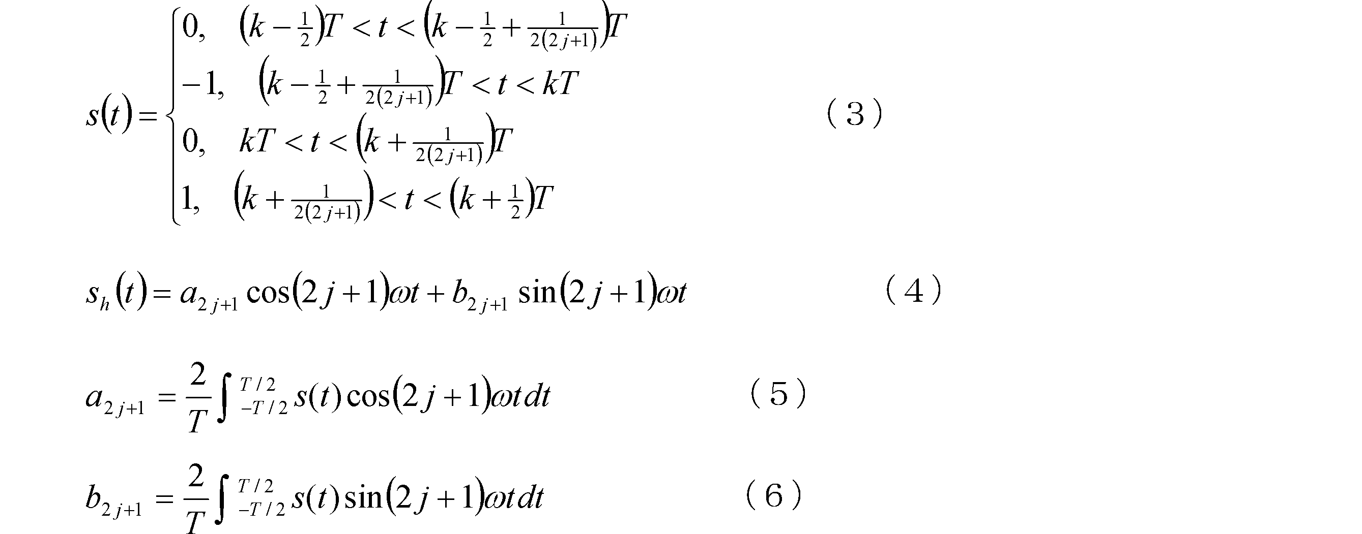
ここで、jは自然数であり、kは整数であり、Tは周期であり、ω=2π/Tは角周波数である。式(5)および式(6)の右辺を計算すると、sh(t)=0が得られる。この結果からわかるように、第1の実施形態の第1の例および第2の例では、駆動電圧に2n+1次高調波が含まれない。このため、駆動電流に2n+1次高調波が含まれないので、駆動電流に2n+1次高調波によるリップルが現れない。
上記のように、スパイク電流およびリップルは、圧電ポンプの実質的な動作に寄与しない無駄な消費電力を増加させる。第1の比較例および第2の比較例では、圧電素子Pのインピーダンスの周波数特性を反映して、駆動電流に2n+1次高調波によるリップルが現れる。第1の実施形態の第1の例では、駆動電圧の休止時間が、1周期当り、T2n+1=T1/(2n+1)である。これにより、駆動電流の2n+1次高調波が抑制されるので、駆動電流に2n+1次高調波によるリップルが現れない。このため、第1の実施形態の第1の例では、第1の比較例および第2の比較例に比べて、圧電素子Pの実質的な動作に寄与しない無駄な消費電力を低減できる。
第1の実施形態の第2の例ではインダクタL1が設けられる。これにより、駆動電流に含まれる高周波成分が除去されるので、駆動電圧が遷移するときに生じるスパイク電流が抑制される。また、インダクタL1と圧電素子Pが有する等価的なキャパシタC1とによる共振が生じて、第1出力端子OUT1と第2出力端子OUT2との間のインピーダンスがさらに小さくなっても、第1の実施形態の第1の例の場合と同様に、駆動電流の2n+1次高調波が抑制される。このため、駆動電流に2n+1次高調波によるリップルが現れない。このため、第1の実施形態の第2の例では、第1の実施形態の第1の例に比べて、さらに無駄な消費電力を低減できる。
第2の比較例でも、インダクタL1が設けられるが、第1の比較例と比べて必ずしも消費電力が低減されない。このため、第1の実施形態の第2の例の圧電素子用駆動回路が有する効果は、駆動電圧が休止時間T2n+1で特徴づけられたステップ波であることと、インダクタL1が設けられることとの相乗効果である。
《第2の実施形態》
第2の実施形態では、駆動電圧の1周期当り、駆動電圧が最大値となる期間と駆動電圧が最小値となる期間とが異なる。第2の実施形態の第1の例は、第1の実施形態の第1の例の場合と同様の回路構成を有する(図1参照)。第2の実施形態の第2の例は、第1の実施形態の第2の例の場合と同様の回路構成を有する(図2参照)。
第2の実施形態では、駆動電圧の1周期当り、駆動電圧が最大値となる期間と駆動電圧が最小値となる期間とが異なる。第2の実施形態の第1の例は、第1の実施形態の第1の例の場合と同様の回路構成を有する(図1参照)。第2の実施形態の第2の例は、第1の実施形態の第2の例の場合と同様の回路構成を有する(図2参照)。
図16は、第2の実施形態の第1の例および第2の例に係る駆動電圧の波形を示す模式図である。駆動電圧の周期はT1である。駆動電圧は、時間T2n+1/2の間、中間電位となり、次の時間TA-T2n+1/2の間、最小値になり、次の時間T2n+1/2の間、中間電位となり、次のT1-TA-T2n+1/2の間、最大値になる。駆動電圧はこの階段状の遷移を周期的に繰返す。時間TAは時間T1/2と異なる値を有する。
図17(A)から図17(D)は、それぞれ、第1の比較例における、第1制御信号、第2制御信号、駆動電圧および駆動電流の波形を示す図である。図17(A)から図17(D)では、圧電素子Pが圧電ポンプに用いられ、その圧電ポンプが流量モードで動作している。流量モードは、圧電ポンプの吸引口および吐出口を開放状態にし、圧電ポンプの吸引口または吐出口の流量を一定にするように圧電ポンプを動作させるモードである。図17(A)から図17(D)では、圧電ポンプとしてサンプル1(図11参照)が用いられている。これらの点は、図18(A)から図18(D)、図19(A)から図19(D)および図20(A)から図20(D)でも同様である。第1制御信号、第2制御信号、駆動電圧および駆動電流の波形は、圧力モードの場合と同様である(図5(A)から図5(D)参照)。
図18(A)から図18(D)は、それぞれ、第2の比較例における、第1制御信号、第2制御信号、駆動電圧および駆動電流の波形を示す図である。第1制御信号、第2制御信号、駆動電圧および駆動電流の波形は、圧力モードの場合と同様である(図6(A)から図6(D)参照)。
図19(A)から図19(D)は、それぞれ、第2の実施形態の第1の例における、第1制御信号、第2制御信号、駆動電圧および駆動電流の波形を示す図である。第1制御信号、第2制御信号、駆動電圧および駆動電流の周波数は約23.5kHzである(周期は約42.6μsである)。第1制御信号および第2制御信号の振幅は約3Vである。駆動電圧の振幅は約24Vである。第1制御信号、第2制御信号および駆動電圧において、時間TAは約20μsであり、n=6、即ち、T2n+1=T13=T1/13である(図16参照)。駆動電流は、駆動電圧が遷移する度に、瞬間的に増大する。駆動電圧が遷移するときの駆動電流は、第1の比較例の場合より小さい。また、駆動電流にはリップルが現れない。
図20(A)から図20(D)は、それぞれ、第2の実施形態の第2の例における、第1制御信号、第2制御信号、駆動電圧および駆動電流の波形を示す図である。第1制御信号、第2制御信号および駆動電圧の波形は第2の実施形態の第1の例の場合と同様である。駆動電圧が遷移するときの駆動電流は、第2の比較例および第1の実施形態の第1の例の場合に比べて小さい。駆動電流にはリップルが現れない。一方、駆動電流には駆動電圧が遷移した時から減衰振動するリンギングが現れる。
図21は、第2の実施形態に係る、流量モードにおける消費電力を示す図である。図21では、第1の比較例における消費電力に対する比率で消費電力が示されている。図21では、圧電ポンプとしてサンプル1(図11参照)が用いられている。第2の比較例では消費電力が約3%削減される。第1の実施形態の第1の例では、消費電力が約12%削減される。第1の実施形態の第2の例では、消費電力が約15%削減される。このように、第2の実施形態の第1の例では、第1の実施形態の第1の例と同等の効果が得られる。第2の実施形態の第2の例では、第1の実施形態の第2の例と同等の効果が得られる。
《第3の実施形態》
第3の実施形態の第1の例では、駆動電圧が中間電位に立ち下がった後に中間電位に留まる時間と、駆動電圧が中間電位まで立ち上がった後に中間電位に留まる時間とが異なる。図22は、第3の実施形態の第1の例に係る駆動電圧の波形を示す模式図である。駆動電圧の周期はT1である。駆動電圧は、時間TBの間、中間電位となり、次の時間T1/2-TBの間、最小値になり、次の時間T2n+1-TBの間、中間電位となり、次のT1/2-(T2n+1-TB)の間、最大値になる。駆動電圧はこの階段状の遷移を周期的に繰返す。時間TBは時間T2n+1/2と異なる値を有する。
第3の実施形態の第1の例では、駆動電圧が中間電位に立ち下がった後に中間電位に留まる時間と、駆動電圧が中間電位まで立ち上がった後に中間電位に留まる時間とが異なる。図22は、第3の実施形態の第1の例に係る駆動電圧の波形を示す模式図である。駆動電圧の周期はT1である。駆動電圧は、時間TBの間、中間電位となり、次の時間T1/2-TBの間、最小値になり、次の時間T2n+1-TBの間、中間電位となり、次のT1/2-(T2n+1-TB)の間、最大値になる。駆動電圧はこの階段状の遷移を周期的に繰返す。時間TBは時間T2n+1/2と異なる値を有する。
第3の実施形態の第2の例では、駆動電圧の休止時間が時間の長さTP1毎に異なる。ここで、時間の長さTP1は、駆動電圧が中間電位に立ち下がる時から次に駆動電圧が中間電位に立ち下がる時までの時間であり、圧電素子Pの基本共振周波数の逆数に略等しい。図23は、第3の実施形態の第2の例に係る駆動電圧の波形を示す模式図である。駆動電圧の周期は2TP1である。駆動電圧は、時間TP 2n+1/2の間、中間電位となり、次の時間(TP1-TP 2n+1)/2の間、最小値になり、次の時間TP 2n+1/2の間、中間電位となり、次の(TP1-TP 2n+1)/2の間、最大値になる。駆動電圧は、次の時間TP 2m+1/2の間、中間電位となり、次の時間(TP1-TP 2m+1)/2の間、最小値になり、次の時間TP 2m+1/2の間、中間電位となり、次の(TP1-TP 2m+1)/2の間、最大値になる。駆動電圧はこの階段状の遷移を周期的に繰返す。ここで、TP 2n+1=TP1/(2n+1)であり、TP 2m+1=TP1/(2m+1)である。n,mは自然数であり、nとmとは互いに異なる。
なお、第3の実施形態の第2の例では、駆動電圧の休止時間が2つの奇数2n+1,2m+1で規定される例を示したが、駆動電圧の休止時間が、2つ以上の奇数で規定されてもよいし、任意に変動してもよい。圧電素子Pのインピーダンスの絶対値が複数の大きなピーク(強いレスポンス)を有する場合、駆動電圧の休止時間が時間の長さTP1毎に異なることが好ましい。
《第4の実施形態》
第4の実施形態に係る圧電素子用駆動回路は自励振式回路である。図24は、第4の実施形態に係る圧電素子用駆動回路30の回路図である。圧電素子用駆動回路30はオペアンプOP1~OP4および抵抗R1を備える。オペアンプOP1~OP3から構成される回路は本発明の「駆動電圧生成部」の一例である。オペアンプOP1の正相入力端子には基準電圧Vc/2が印加される。オペアンプOP1の逆相入力端子はオペアンプOP4の出力端子に接続される。オペアンプOP1の出力端子は、オペアンプOP2の正相入力端子およびオペアンプOP3の逆相入力端子に接続される。オペアンプOP2の逆相入力端子には基準電圧Vc/2+dVが印加される。オペアンプOP2の出力端子は圧電素子Pの第1端子に接続される。オペアンプOP3の正相入力端子には基準電圧Vc/2-dVが印加される。オペアンプOP3の出力端子は、抵抗R1を介して、圧電素子Pの第2端子に接続される。オペアンプOP4の正相入力端子および逆相入力端子は、それぞれ、抵抗R1の第1端子および第2端子に接続される。オペアンプOP1~OP4の正電源端子にはVcが印加される。オペアンプOP1~OP4の負電源端子は接地される。圧電素子用駆動回路30の各回路素子の特性は、圧電素子Pの基本共振周波数で、バルクハウゼンの発振条件を満たすように定められる。このため、圧電素子用駆動回路30は圧電素子Pの基本共振周波数で圧電素子Pを駆動する。
第4の実施形態に係る圧電素子用駆動回路は自励振式回路である。図24は、第4の実施形態に係る圧電素子用駆動回路30の回路図である。圧電素子用駆動回路30はオペアンプOP1~OP4および抵抗R1を備える。オペアンプOP1~OP3から構成される回路は本発明の「駆動電圧生成部」の一例である。オペアンプOP1の正相入力端子には基準電圧Vc/2が印加される。オペアンプOP1の逆相入力端子はオペアンプOP4の出力端子に接続される。オペアンプOP1の出力端子は、オペアンプOP2の正相入力端子およびオペアンプOP3の逆相入力端子に接続される。オペアンプOP2の逆相入力端子には基準電圧Vc/2+dVが印加される。オペアンプOP2の出力端子は圧電素子Pの第1端子に接続される。オペアンプOP3の正相入力端子には基準電圧Vc/2-dVが印加される。オペアンプOP3の出力端子は、抵抗R1を介して、圧電素子Pの第2端子に接続される。オペアンプOP4の正相入力端子および逆相入力端子は、それぞれ、抵抗R1の第1端子および第2端子に接続される。オペアンプOP1~OP4の正電源端子にはVcが印加される。オペアンプOP1~OP4の負電源端子は接地される。圧電素子用駆動回路30の各回路素子の特性は、圧電素子Pの基本共振周波数で、バルクハウゼンの発振条件を満たすように定められる。このため、圧電素子用駆動回路30は圧電素子Pの基本共振周波数で圧電素子Pを駆動する。
オペアンプOP4は、駆動電流に比例する電圧を検出して、その電圧を差動増幅する。オペアンプOP1は、オペアンプOP1の出力信号と基準電圧Vc/2との差分を増幅する。オペアンプOP1は反転増幅回路である。オペアンプOP1の出力信号は略台形波である。オペアンプOP2は、オペアンプOP1の出力信号と基準電圧Vc/2+dVとの差分を増幅する。オペアンプOP2は非反転増幅回路である。オペアンプOP3は、オペアンプOP1の出力信号と基準電圧Vc/2-dVとの差分を増幅する。オペアンプOP3は反転増幅回路である。オペアンプOP1の出力信号が基準電圧Vc/2+dV以上になる期間は、オペアンプOP1の出力信号が基準電圧Vc/2-dV以上になる期間と異なる。このため、オペアンプOP2の出力端子とオペアンプOP3の出力端子との間の電位差は、中間電位を経て略階段状に遷移するステップ波となる(図3参照)。第4の実施形態では、第1の実施形態と同様の効果が得られる。
なお、上記の実施形態では、駆動電圧の中間電位が駆動電圧の最大値と駆動電圧の最小値の中央値に定められる例を示したが、該中間電位は、該中央値より該最小値に近い値、または、該中央値より該最大値に近い値に定められてもよい。図25(A)には、中間電位VMが中央値V0より最小値に近い値をとる駆動電圧の波形が示されている。図25(B)には、中間電位VMが中央値V0より最大値に近い値をとる駆動電圧の波形が示されている。
また、上記の実施形態では、駆動電圧が遷移する電位が最大値と最小値との間に1つ存在する例を示したが、駆動電圧が遷移する電位が最大値と最小値との間に複数存在してもよい。即ち、駆動電圧は、最大値、最小値および複数の中間電位に遷移してもよい。
また、上記の実施形態では、インダクタが設けられる例を示したが、駆動電流の高周波成分を除去できる別の素子または回路が設けられてもよい。
また、上記の実施形態では、駆動電圧を規定する奇数2n+1が、圧電素子のインピーダンスの絶対値のピークのうちピークの高さが最も大きいものから定められる例を示したが、奇数2n+1は圧電素子のインピーダンスの絶対値の他のピークから定められてもよい。
IN1…第1入力端子
IN2…第2入力端子
L1…インダクタ
OP1~OP4…オペアンプ
OUT1…第1出力端子
OUT2…第2出力端子
P…圧電素子
R1…抵抗
10,20,30…圧電素子用駆動回路(駆動電圧生成部)
11…ブリッジ回路
12…制御信号発生部
IN2…第2入力端子
L1…インダクタ
OP1~OP4…オペアンプ
OUT1…第1出力端子
OUT2…第2出力端子
P…圧電素子
R1…抵抗
10,20,30…圧電素子用駆動回路(駆動電圧生成部)
11…ブリッジ回路
12…制御信号発生部
Claims (7)
- 所定の周波数で駆動し、該所定の周波数の(2n+1)倍の共振周波数(nは所定の自然数)を有した圧電素子と、
前記圧電素子の第1端子に接続される第1出力端子、および、前記圧電素子の第2端子に接続される第2出力端子を有する駆動電圧生成部を備え、
前記圧電素子が駆動されるとき、前記第1出力端子と前記第2出力端子との間の電位差の波形は、中間電位を経て遷移するステップ波となり、
前記電位差が前記中間電位となる時間の長さは、前記電位差が前記中間電位に立ち下がる時間t1から次に前記電位差が前記中間電位に立ち下がる時間t2までの間において、(t2-t1)/(2n+1)付近である圧電素子用駆動回路。 - 前記所定の周波数の(2n+1)倍の共振周波数における前記圧電素子のインピーダンスの絶対値のピークの高さが、前記所定の周波数における前記圧電素子のインピーダンスの絶対値のピークの高さより高い、請求項1に記載の圧電素子用駆動回路。
- 前記所定の周波数の(2n+1)倍の共振周波数における前記圧電素子のインピーダンスの絶対値のピークの高さが、前記圧電素子の共振周波数における前記圧電素子のインピーダンスの絶対値のピークの中で、最も高い、請求項1または2に記載の圧電素子用駆動回路。
- 第1制御信号出力端子および第2制御信号出力端子を有する制御信号発生部を備え、
前記駆動電圧生成部は、前記第1制御信号出力端子に接続される第1入力端子、および、前記第2制御信号出力端子に接続される第2入力端子を有する、請求項1から3の何れかに記載の圧電素子用駆動回路。 - 前記第1出力端子と前記圧電素子の第1端子との間に直列接続されるインダクタを備える、請求項1から4の何れかに記載の圧電素子用駆動回路。
- 前記電位差が前記中間電位となるとき、前記圧電素子側から前記駆動電圧生成部側を見て、前記第1出力端子および前記第2出力端子は開放状態である、請求項1から5の何れかに記載の圧電素子用駆動回路。
- 前記電位差が前記中間電位となるとき、前記第1出力端子と前記第2出力端子との間に電圧0Vが印加される、請求項1から5の何れかに記載の圧電素子用駆動回路。
Priority Applications (3)
| Application Number | Priority Date | Filing Date | Title |
|---|---|---|---|
| JP2018516984A JP6662452B2 (ja) | 2016-05-11 | 2017-05-02 | 圧電素子用駆動回路 |
| US16/173,029 US11098705B2 (en) | 2016-05-11 | 2018-10-29 | Piezoelectric element drive circuit |
| US17/376,553 US11592017B2 (en) | 2016-05-11 | 2021-07-15 | Piezoelectric element drive circuit |
Applications Claiming Priority (2)
| Application Number | Priority Date | Filing Date | Title |
|---|---|---|---|
| JP2016094964 | 2016-05-11 | ||
| JP2016-094964 | 2016-05-11 |
Related Child Applications (1)
| Application Number | Title | Priority Date | Filing Date |
|---|---|---|---|
| US16/173,029 Continuation US11098705B2 (en) | 2016-05-11 | 2018-10-29 | Piezoelectric element drive circuit |
Publications (1)
| Publication Number | Publication Date |
|---|---|
| WO2017195701A1 true WO2017195701A1 (ja) | 2017-11-16 |
Family
ID=60266555
Family Applications (1)
| Application Number | Title | Priority Date | Filing Date |
|---|---|---|---|
| PCT/JP2017/017236 Ceased WO2017195701A1 (ja) | 2016-05-11 | 2017-05-02 | 圧電素子用駆動回路 |
Country Status (3)
| Country | Link |
|---|---|
| US (2) | US11098705B2 (ja) |
| JP (1) | JP6662452B2 (ja) |
| WO (1) | WO2017195701A1 (ja) |
Families Citing this family (2)
| Publication number | Priority date | Publication date | Assignee | Title |
|---|---|---|---|---|
| JP7079352B2 (ja) * | 2018-07-03 | 2022-06-01 | シーメンス・ヘルスケア・ダイアグノスティックス・インコーポレイテッド | ピペット装置の近接感知のために無脈動空気流を生成する小型圧電空気ポンプ |
| FR3158455A1 (fr) * | 2024-01-23 | 2025-07-25 | L'oreal | Dispositif de distribution de produit fluide, appareil et procédé associés |
Citations (11)
| Publication number | Priority date | Publication date | Assignee | Title |
|---|---|---|---|---|
| JPS55144297A (en) * | 1979-04-27 | 1980-11-11 | Fuji Electrochemical Co Ltd | Piezoelectric sound generator |
| JPS58198173A (ja) * | 1982-05-11 | 1983-11-18 | Olympus Optical Co Ltd | 圧電形回転装置 |
| JPH01158810A (ja) * | 1987-12-15 | 1989-06-21 | Murata Mfg Co Ltd | 電歪効果素子の製造方法 |
| JP2000184759A (ja) * | 1998-12-10 | 2000-06-30 | Canon Inc | 振動型アクチュエ―タ駆動装置 |
| JP2003164172A (ja) * | 2001-11-21 | 2003-06-06 | Minolta Co Ltd | 駆動装置 |
| JP2003189644A (ja) * | 2001-12-18 | 2003-07-04 | Minolta Co Ltd | 駆動装置 |
| JP4744636B1 (ja) * | 2010-02-12 | 2011-08-10 | マクセルファインテック株式会社 | 駆動装置、画像取得装置および電子機器 |
| JP2011199102A (ja) * | 2010-03-23 | 2011-10-06 | Koji Toda | 振動発電素子 |
| WO2013084709A1 (ja) * | 2011-12-09 | 2013-06-13 | 株式会社村田製作所 | 圧電素子用駆動回路 |
| JP2013121308A (ja) * | 2011-12-09 | 2013-06-17 | Murata Mfg Co Ltd | 圧電素子用駆動回路 |
| WO2015079736A1 (ja) * | 2013-11-27 | 2015-06-04 | 株式会社村田製作所 | 駆動装置 |
Family Cites Families (3)
| Publication number | Priority date | Publication date | Assignee | Title |
|---|---|---|---|---|
| JP5151163B2 (ja) * | 2007-01-30 | 2013-02-27 | コニカミノルタアドバンストレイヤー株式会社 | 駆動装置、および駆動システム |
| GB201222882D0 (en) | 2012-12-19 | 2013-01-30 | Univ Leeds | Ultrasound generation |
| JP6332454B2 (ja) | 2014-07-14 | 2018-05-30 | 株式会社村田製作所 | 圧電素子用駆動回路および吸引装置 |
-
2017
- 2017-05-02 JP JP2018516984A patent/JP6662452B2/ja active Active
- 2017-05-02 WO PCT/JP2017/017236 patent/WO2017195701A1/ja not_active Ceased
-
2018
- 2018-10-29 US US16/173,029 patent/US11098705B2/en active Active
-
2021
- 2021-07-15 US US17/376,553 patent/US11592017B2/en active Active
Patent Citations (11)
| Publication number | Priority date | Publication date | Assignee | Title |
|---|---|---|---|---|
| JPS55144297A (en) * | 1979-04-27 | 1980-11-11 | Fuji Electrochemical Co Ltd | Piezoelectric sound generator |
| JPS58198173A (ja) * | 1982-05-11 | 1983-11-18 | Olympus Optical Co Ltd | 圧電形回転装置 |
| JPH01158810A (ja) * | 1987-12-15 | 1989-06-21 | Murata Mfg Co Ltd | 電歪効果素子の製造方法 |
| JP2000184759A (ja) * | 1998-12-10 | 2000-06-30 | Canon Inc | 振動型アクチュエ―タ駆動装置 |
| JP2003164172A (ja) * | 2001-11-21 | 2003-06-06 | Minolta Co Ltd | 駆動装置 |
| JP2003189644A (ja) * | 2001-12-18 | 2003-07-04 | Minolta Co Ltd | 駆動装置 |
| JP4744636B1 (ja) * | 2010-02-12 | 2011-08-10 | マクセルファインテック株式会社 | 駆動装置、画像取得装置および電子機器 |
| JP2011199102A (ja) * | 2010-03-23 | 2011-10-06 | Koji Toda | 振動発電素子 |
| WO2013084709A1 (ja) * | 2011-12-09 | 2013-06-13 | 株式会社村田製作所 | 圧電素子用駆動回路 |
| JP2013121308A (ja) * | 2011-12-09 | 2013-06-17 | Murata Mfg Co Ltd | 圧電素子用駆動回路 |
| WO2015079736A1 (ja) * | 2013-11-27 | 2015-06-04 | 株式会社村田製作所 | 駆動装置 |
Also Published As
| Publication number | Publication date |
|---|---|
| US20210340970A1 (en) | 2021-11-04 |
| JPWO2017195701A1 (ja) | 2019-01-31 |
| US11592017B2 (en) | 2023-02-28 |
| US11098705B2 (en) | 2021-08-24 |
| US20190067555A1 (en) | 2019-02-28 |
| JP6662452B2 (ja) | 2020-03-11 |
Similar Documents
| Publication | Publication Date | Title |
|---|---|---|
| JP5716843B2 (ja) | 圧電素子用駆動回路 | |
| CN102651604B (zh) | 纹波调节器的控制电路及方法 | |
| JP6101463B2 (ja) | Dc/dc変換器のためのコントローラ | |
| JP2010207022A (ja) | Dc−dcコンバータの制御回路、dc−dcコンバータ、dc−dcコンバータの制御方法 | |
| JP6662452B2 (ja) | 圧電素子用駆動回路 | |
| JP6332454B2 (ja) | 圧電素子用駆動回路および吸引装置 | |
| JP5696414B2 (ja) | 電圧生成回路 | |
| JP7219722B2 (ja) | ポンプ装置 | |
| JP2003134799A5 (ja) | ||
| JP2003164163A (ja) | 圧電トランス駆動回路 | |
| JP2004180294A (ja) | 電力増幅装置 | |
| CN111796150A (zh) | 占空比检测电路及占空比检测方法 | |
| TW201404020A (zh) | 負電壓產生電路 | |
| JP2005151689A (ja) | 同期整流方式スイッチングレギュレータ制御回路及びこれを含む半導体集積回路 | |
| JP2013121308A (ja) | 圧電素子用駆動回路 | |
| JP6011389B2 (ja) | 電源制御回路および電源装置 | |
| CN105612686B (zh) | 电压供给电路及其控制方法 | |
| JP2005295754A (ja) | スイッチングレギュレータ | |
| JP2016106519A (ja) | 圧電素子用駆動回路 | |
| JP2012175238A (ja) | 電子回路 | |
| KR20150102795A (ko) | 부하에 적응하여 구동주파수가 가변되는 부스팅회로 |
Legal Events
| Date | Code | Title | Description |
|---|---|---|---|
| WWE | Wipo information: entry into national phase |
Ref document number: 2018516984 Country of ref document: JP |
|
| NENP | Non-entry into the national phase |
Ref country code: DE |
|
| 121 | Ep: the epo has been informed by wipo that ep was designated in this application |
Ref document number: 17796062 Country of ref document: EP Kind code of ref document: A1 |
|
| 122 | Ep: pct application non-entry in european phase |
Ref document number: 17796062 Country of ref document: EP Kind code of ref document: A1 |