WO2017195419A1 - 透明導電性フィルム及びその製造方法 - Google Patents
透明導電性フィルム及びその製造方法 Download PDFInfo
- Publication number
- WO2017195419A1 WO2017195419A1 PCT/JP2017/004534 JP2017004534W WO2017195419A1 WO 2017195419 A1 WO2017195419 A1 WO 2017195419A1 JP 2017004534 W JP2017004534 W JP 2017004534W WO 2017195419 A1 WO2017195419 A1 WO 2017195419A1
- Authority
- WO
- WIPO (PCT)
- Prior art keywords
- transparent conductive
- indium tin
- resin film
- dielectric layer
- composite oxide
- Prior art date
- Legal status (The legal status is an assumption and is not a legal conclusion. Google has not performed a legal analysis and makes no representation as to the accuracy of the status listed.)
- Ceased
Links
Images

Classifications
-
- B—PERFORMING OPERATIONS; TRANSPORTING
- B32—LAYERED PRODUCTS
- B32B—LAYERED PRODUCTS, i.e. PRODUCTS BUILT-UP OF STRATA OF FLAT OR NON-FLAT, e.g. CELLULAR OR HONEYCOMB, FORM
- B32B9/00—Layered products comprising a layer of a particular substance not covered by groups B32B11/00 - B32B29/00
-
- H—ELECTRICITY
- H01—ELECTRIC ELEMENTS
- H01B—CABLES; CONDUCTORS; INSULATORS; SELECTION OF MATERIALS FOR THEIR CONDUCTIVE, INSULATING OR DIELECTRIC PROPERTIES
- H01B13/00—Apparatus or processes specially adapted for manufacturing conductors or cables
-
- H—ELECTRICITY
- H01—ELECTRIC ELEMENTS
- H01B—CABLES; CONDUCTORS; INSULATORS; SELECTION OF MATERIALS FOR THEIR CONDUCTIVE, INSULATING OR DIELECTRIC PROPERTIES
- H01B5/00—Non-insulated conductors or conductive bodies characterised by their form
- H01B5/14—Non-insulated conductors or conductive bodies characterised by their form comprising conductive layers or films on insulating-supports
Definitions
- the present invention relates to a transparent conductive film in which an indium tin composite oxide layer is disposed on one side of a resin film and a method for producing the same.
- a transparent conductive film in which a transparent conductive thin film such as an indium tin composite oxide layer is formed on a transparent substrate is widely used in devices such as displays and touch panels. In these devices, the transparent conductive film is used for parts that require both transparency and conductivity.
- Patent Document 1 proposes a technique of providing an adhesion improving layer made of a metal oxide having a low crystallinity on a transparent conductive thin film.
- Patent Document 1 since a metal oxide layer generally composed of a metal oxide having a low degree of crystallinity is inferior in transparency or conductivity, in Patent Document 1, the adhesion improving layer is the conductivity or transparency of the transparent conductive film. May worsen sex.
- the present invention provides a transparent conductive film having high conductivity and transparency without providing an adhesion improving layer, and improved adhesion with an extraction electrode, and a method for producing the same I will provide a.
- the present invention provides a transparent conductive film in which a dielectric layer and an indium tin composite oxide layer are arranged in this order on one surface of a resin film.
- the resin film includes a polyester resin film, a cellulose resin film, and It is a kind selected from the group consisting of imide resin films, and the dielectric layer is composed of an organic substance or a mixture of an organic substance and an inorganic substance, and has a thickness of 0.005 ⁇ m to 0.100 ⁇ m, and the indium tin composite
- An active hydrogen group that can be chemically modified with trifluoroacetic anhydride is present at 2.1 atomic% to 4.0 atomic% on the surface of the oxide layer opposite to the side where the dielectric layer is disposed.
- the present invention relates to a transparent conductive film.
- the present invention also comprises an organic substance or a mixture of an organic substance and an inorganic substance on one surface of one kind of resin film selected from the group consisting of a polyester resin film, a cellulose resin film and an imide resin film, and has a thickness. Is laminated with a dielectric layer of 0.005 ⁇ m or more and 0.100 ⁇ m or less, and an indium tin composite oxide layer is laminated on the surface of the dielectric layer opposite to the side where the resin film is disposed, An active hydrogen that can be chemically modified with trifluoroacetic anhydride on the surface of the indium tin composite oxide layer opposite to the side on which the dielectric layer is disposed.
- the present invention relates to a method for producing a transparent conductive film, characterized in that a transparent conductive film having a group of 2.1 atomic% or more and 4.0 atomic% or less is obtained.
- the present invention provides a transparent conductive film having high conductivity and transparency and improved adhesion to the extraction electrode. Moreover, according to the manufacturing method of this invention, the transparent conductive film which has high electroconductivity and transparency, and the adhesiveness with the extraction electrode can be produced simply.
- FIG. 1 is a schematic cross-sectional view of a transparent conductive film according to an embodiment of the present invention.
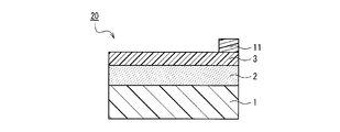
- FIG. 2 is a schematic cross-sectional view of a transparent conductive film according to another embodiment of the present invention.
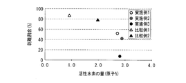
- FIG. 3 is a graph showing the relationship between the amount of active hydrogen groups that can be chemically modified with trifluoroacetic anhydride present on the surface of the indium tin composite oxide layer and the peeling rate between the transparent conductive film and the extraction electrode. is there.
- the present inventors diligently studied to improve the adhesion with the extraction electrode while keeping the conductivity and transparency of the transparent conductive film high.
- a resin film selected from the group consisting of a polyester-based resin film, a cellulose-based resin film, and an imide-based resin film is used as the transparent substrate, and an indium tin composite oxide layer is used as the transparent conductive film.
- a dielectric layer made of an organic material or a mixture of an organic material and an inorganic material having a thickness of 0.005 ⁇ m to 0.100 ⁇ m is disposed between the surface of the indium tin composite oxide layer and the indium tin composite oxide layer.
- the active hydrogen group that can be chemically modified with trifluoroacetic anhydride is present in an amount of 2.1 atomic% (atomic%) to 4.0 atomic%, thereby providing high conductivity and transparency, and an extraction electrode.
- the present inventors have found that a transparent conductive film having improved adhesion can be obtained, and the present invention has been achieved.
- the transparent conductive film of the present invention has high adhesion to the extraction electrode, in the touch panel using the metal extraction electrode, the signal of the touch sensor formed of the transparent conductive film can be reliably acquired by the extraction electrode. As a result, the reliability of the touch sensor is improved.
- the adhesion with the extraction electrode is high, the function of the touch sensor composed of the transparent conductive film is maintained well even after the heating and humidification test, and the durability of the touch sensor is improved.
- FIG. 1 is a schematic cross-sectional view of a transparent conductive film according to an embodiment of the present invention.
- the transparent conductive film 10 includes a resin film 1, a dielectric layer 2 disposed on one surface of the resin film 1, and a resin film 1 of the dielectric layer 2. And an indium tin composite oxide layer 3 disposed on the surface opposite the coated side.
- indium tin composite oxide is synonymous with ITO (Indium Tin Oxide).
- the resin film 1 is a kind selected from the group consisting of a polyester resin film, a cellulose resin film, and an imide resin film.
- a polyester resin, a cellulose resin, and an imide resin have an appropriate water content (also referred to as a moisture content) by having a polar group in the molecular skeleton. Therefore, in the transparent conductive film 10, the moisture contained in the resin film 1 formed of a resin having a polar group in these molecular skeletons causes the indium tin composite oxide layer to form the indium tin composite oxide layer.
- the polyester resin is not particularly limited, but a copolymer of a dicarboxylic acid component and a diol component can be used.
- a polyester resin can be obtained, for example, by using a dicarboxylic acid component and a diol component as raw materials and subjecting these components to an esterification reaction or a polycondensation reaction.
- the dicarboxylic acid component is not particularly limited.
- malonic acid succinic acid, glutaric acid, adipic acid, suberic acid, sebacic acid, dodecanedioic acid, dimer acid, eicosandioic acid, pimelic acid, azelaic acid
- Aliphatic dicarboxylic acids such as methylmalonic acid and ethylmalonic acid
- alicyclic dicarboxylic acids such as adamantane dicarboxylic acid, norbornene dicarboxylic acid, cyclohexanedicarboxylic acid, decalin dicarboxylic acid
- terephthalic acid isophthalic acid, phthalic acid, 1,4- Naphthalene dicarboxylic acid, 1,5-naphthalene dicarboxylic acid, 2,6-naphthalene dicarboxylic acid, 1,8-naphthalene dicarboxylic acid, 4,4′-diphenyl dicar
- the dicarboxylic acid component it is preferable that at least one aromatic dicarboxylic acid is used. More preferably, the dicarboxylic acid component contains an aromatic dicarboxylic acid as a main component.
- the “main component” means that the proportion of aromatic dicarboxylic acid in the dicarboxylic acid component is 80% by mass or more.
- the diol component is not particularly limited.
- ethylene glycol, 1,2-propanediol, 1,3-propanediol, 1,4-butanediol, 1,2-butanediol, 1,3-butanediol Aliphatic diols such as cyclohexanedimethanol, spiroglycol and isosorbide; bisphenol A, 1,3-benzenedimethanol, 1,4-benzenedimethanol, 9,9′-bis (4 And aromatic diols such as -hydroxyphenyl) fluorene.
- the said diol component may be used by 1 type and may use 2 or more types together.
- the diol component at least one aliphatic diol is preferably used.
- the aliphatic diol can contain ethylene glycol, and preferably contains ethylene glycol as a main component.
- the “main component” means that the proportion of ethylene glycol in the diol component is 80% by mass or more.
- the polyester resin obtained using the dicarboxylic acid component and the diol component is not particularly limited.
- PET polyethylene terephthalate
- PEN polyethylene-2,6-naphthalate
- PBT polybutylene terephthalate
- PET is more preferable from the viewpoint of cost.
- the cellulose-based resin is not particularly limited.
- cellulose and / or a cellulose ester that is a derivative thereof is preferable.
- the cellulose ester is preferably an ester of cellulose and a fatty acid (including an aromatic fatty acid), and the hydroxyl groups at the 2nd, 3rd and 6th positions of ⁇ -1,4 linked glucose units constituting the cellulose are represented by the above fatty acid.
- a cellulose acylate substituted with an acyl group and acylated is preferred. Examples thereof include cellulose alkylcarbonyl esters, alkenylcarbonyl esters, aromatic carbonyl esters, and aromatic alkylcarbonyl esters. These cellulose acylates are preferable even if the acyl groups of two or more fatty acids are substituted. Furthermore, you may have another substituent.
- an acetyl group having 2 carbon atoms and an acyl group having 3 to 22 carbon atoms can be preferably used.
- the acyl group may be appropriately determined according to required optical properties, thermal properties, mechanical properties, resin surface free energy, compatibility, and the like.
- the substitution degree of the acyl group in the cellulose ester used in the present invention is not particularly limited.
- the degree of substitution may be appropriately determined according to required optical characteristics, thermal characteristics, mechanical characteristics, resin surface free energy, compatibility, and the like.
- the acyl group may be aliphatic or aromatic and is not particularly limited.
- acetyl group, propionyl group, butanoyl group, benzoyl group, naphthylcarbonyl group and the like are preferable.
- Examples of the cellulose ester substituted with the acyl group include cellulose acetate, cellulose propionate, cellulose butyrate, cellulose acetate naphthalate, and cellulose benzoate.
- the imide resin is not particularly limited, but an imidized copolymer of a diamine component and a carboxylic dianhydride component can be used.
- a resin obtained by polymerizing and imidizing these components using a diamine component and a carboxylic dianhydride component as raw materials can be used.
- the diamine component is not particularly limited.
- carboxylic dianhydride component is not particularly limited, for example, ethylene tetracarboxylic dianhydride, butane tetracarboxylic dianhydride, cyclobutane tetracarboxylic dianhydride, cyclopentane tetracarboxylic dianhydride, 3 , 3 ′, 4,4′-benzophenone tetracarboxylic dianhydride, 2,2 ′, 3,3′-benzophenone tetracarboxylic dianhydride, 3,3 ′, 4,4′-biphenyltetracarboxylic dianhydride Anhydride, 2,2-bis (3,4-dicarboxyphenyl) propane dianhydride, 2,2-bis (2,3-dicarboxyphenyl) propane dianhydride, bis (3,4-dicarboxyphenyl) ) Ether dianhydride, bis (3,4-dicarboxyphenyl) sulfone dianhydride
- Resin film 1 that is, a kind of resin film selected from the group consisting of a polyester resin film, a cellulose resin film and an imide resin film is preferably colorless and transparent at least in the visible light region.
- a polyethylene terephthalate film PET film
- PET film polyethylene terephthalate film
- the PET film is not particularly limited, and examples thereof include an unstretched film, a uniaxially stretched film, a biaxially stretched film, and an obliquely stretched film.
- a biaxially stretched film in which molecules are oriented by biaxial stretching is preferable from the viewpoint of excellent mechanical properties and heat resistance.
- the thickness of the resin film 1, such as a PET film is preferably 15 ⁇ m to 250 ⁇ m, more preferably 20 ⁇ m to 190 ⁇ m, further preferably 45 ⁇ m to 130 ⁇ m, and particularly preferably 45 ⁇ m to 55 ⁇ m. If the thickness is within the above range, since the resin film 1 such as a PET film has durability and appropriate flexibility, the dielectric layer 2 and the indium tin composite oxide layer 3 are roll-to- The roll method makes it possible to form a film with high productivity.
- the resin film 1, such as a PET film, is not particularly limited, but from the viewpoint of improving the adhesion between the transparent conductive film and the extraction electrode, surface treatment such as corona treatment or plasma treatment is performed on the surface on which the dielectric layer 2 is disposed. It is preferable that it is given.
- the resin film 1 such as a PET film
- the resin film 1 is hard coated on the surface opposite to the side where the dielectric layer 2 and the indium tin composite oxide layer 3 are disposed. What formed the layer (not shown) is used suitably. When it has a hard coat layer, the scratch resistance is improved, and the handleability during touch panel processing is improved.
- the hard coat layer can be formed, for example, by curing a thermosetting resin composition or an ultraviolet curable resin composition. It is preferable from the viewpoint of productivity to use a radical polymerization type ultraviolet curable resin composition.
- the ultraviolet curable resin composition usually contains an unsaturated monomer, oligomer, and / or resin, a photopolymerization initiator, and the like.
- an ultraviolet curable resin composition containing a polyfunctional ultraviolet curable acrylic compound and a photopolymerization initiator can be used.
- the polyfunctional ultraviolet curable acrylic compound include polyfunctional acrylates, polyfunctional urethane acrylates, polyfunctional polyester acrylates having two or more functional groups. A well-known thing can be used as a photoinitiator.
- the thickness of the hard coat layer is preferably 0.5 ⁇ m to 5.0 ⁇ m, more preferably 0.6 ⁇ m to 2.0 ⁇ m from the viewpoint of surface hardness and flexibility.
- a hard-coat layer is not specifically limited, It can form using a wet method (coating method).
- a transparent conductive film In a transparent conductive film, from the viewpoint of improving the invisibility after pattern formation of an indium tin composite oxide layer (also referred to as a transparent conductive layer or a transparent conductive film), a transparent substrate such as a resin film and indium tin A dielectric layer having an optical adjustment function may be provided between the composite oxide layer.
- the dielectric layer 2 has an optical adjustment function, and in addition to improving the invisibility after the pattern formation of the indium tin composite oxide layer by the optical adjustment function, as described later
- the indium tin composite oxide layer 3 has a function of adjusting the amount of active hydrogen groups present on the surface.
- the “active hydrogen group” means an active hydrogen group that can be chemically modified with trifluoroacetic anhydride unless otherwise specified.
- a dielectric layer 2 having a thickness of 0.005 ⁇ m to 0.100 ⁇ m and composed of an organic material or a mixture of an organic material and an inorganic material is disposed on one surface of a resin film 1, for example, a polyester-based resin film.
- Indium tin composite oxide layer 3 is formed on the surface of dielectric layer 2 by sputtering or the like by disposing indium tin composite oxide layer 3 on the surface opposite to the side on which resin film 1 of 2 is disposed
- moisture from the resin film 1 such as a polyester-based resin film moves to the surface of the indium tin composite oxide layer 3. Therefore, the surface of the indium tin composite oxide layer 3 is chemically treated with trifluoroacetic anhydride. It is presumed that there will be 2.1 atomic% to 4.0 atomic% of active hydrogen groups that can be modified.
- the transparent conductive film 10 When the transparent conductive film 10 functions as a touch sensor, it is necessary to form a pattern on the indium tin composite oxide layer 3.
- the transmittance, reflectance, and color difference between the portion where the indium tin composite oxide layer 3 exists and the portion where the indium tin composite oxide layer 3 does not exist are different.
- the dielectric layer 2 having an optical adjustment function, an optical transmittance difference, a reflectance difference between a portion where the indium tin composite oxide layer 3 exists and a portion where the indium tin composite oxide layer 3 does not exist, and By reducing the color difference, the pattern is less visible.
- the dielectric layer 2 is composed of an organic material or a mixture of an organic material and an inorganic material.
- an organic substance in the dielectric layer 2 it becomes easy to adjust the active hydrogen groups present on the surface of the indium tin composite oxide layer 3 on the side opposite to the side where the dielectric layer 2 is disposed within a predetermined range.
- organic substances include acrylic resins, urethane resins, melamine resins, alkyd resins, siloxane polymers, and organosilane condensates.
- silicon oxide also referred to as silica
- aluminum oxide, zirconium oxide, titanium oxide and the like are preferably used from the viewpoint of easy control of the refractive index.
- a mixture of one or more inorganic particles selected from the group consisting of silicon oxide, aluminum oxide, zirconium oxide, and titanium oxide and an acrylic resin, or a siloxane polymer is preferably used.
- the particle size of the inorganic particles is reduced, the light transmittance tends to be lowered due to a decrease in dispersibility.
- the average particle diameter is preferably 5 nm to 100 nm, more preferably 10 to 20 nm.
- acrylic resin what hardened the resin composition containing polyfunctional urethane acrylate and a photoinitiator is mentioned, for example.
- an alkoxysilane hydrolyzed condensate obtained by condensing an alkoxysilane hydrolyzate and organic silica sol particles is preferably used.
- the active hydrogen groups on the surface of the indium tin composite oxide layer 3 can be easily adjusted to a predetermined range, and the surface of the transparent conductive film Roughness can be adjusted to an appropriate range to improve durability.
- the average particle diameter of inorganic particles means a value obtained by weighted average of particle diameters in a cross-sectional image obtained by a transmission electron microscope.
- the dielectric layer 2 may be a single layer or a plurality of layers of two or more layers. From the viewpoint of productivity, one layer is preferable. Two or more layers are preferable from the viewpoint of the balance of transmittance, reflectance, and color difference. In the case of a multi-layer structure of two or more layers, the refractive index of the dielectric layer 2 on the side close to the resin film 1 is increased and the dielectric on the side far from the resin film 1 from the viewpoint of the balance of transmittance, reflectance and color difference. It is preferable to lower the refractive index of the body layer 2. From the viewpoint of good optical adjustment function, the dielectric layer 2 preferably has a refractive index of 1.30 to 1.80, more preferably 1.40 to 1.60, and 1.50 to 1. More preferably, it is .60.
- the dielectric layer 2 has a thickness in the range of 0.005 ⁇ m to 0.100 ⁇ m, the amount of active hydrogen groups present on the surface of the indium tin composite oxide layer 3 can be easily adjusted to a predetermined range.
- the total thickness of all the layers is defined as the thickness of the dielectric layer 2. Further, when the thickness of the dielectric layer 2 is in the above-described range, the optical adjustment function and the adhesion with the extraction electrode are also improved.
- the thickness of the dielectric layer 2 exceeds 0.100 ⁇ m, the adhesion between the indium tin composite oxide layer 3 and the extraction electrode decreases due to the film stress, and the thickness of the dielectric layer 2 is less than 0.005 ⁇ m. As a result, the optical adjustment function deteriorates.
- the thickness of the dielectric layer 2 is preferably 0.015 ⁇ m to 0.040 ⁇ m, and preferably 0.020 ⁇ m to 0.035 ⁇ m. It is more preferable that the thickness is 0.025 ⁇ m to 0.030 ⁇ m.
- the dielectric layer 2 can be formed by a dry process such as a vacuum deposition method, a sputtering method, or an ion plating method, or a wet method (coating method). Among these, the wet method is preferable from the viewpoint of productivity.
- the indium tin composite oxide layer 3 is a metal oxide thin film made of indium tin oxide (Indium Tin Oxide).
- the indium tin composite oxide layer 3 contains 88% to 98% by weight of indium oxide when the total weight of indium oxide and tin oxide is 100% by weight from the viewpoint of achieving both transparency and low resistance. It is preferable to contain 2% to 12% by weight of tin oxide, 90% to 97% by weight of indium oxide, more preferably 3% to 10% by weight of tin oxide, and 92% of indium oxide. More preferably, it is contained in an amount of 95% by weight to 95% by weight and tin oxide is contained in an amount of 5% by weight to 8% by weight. When the content of tin oxide is within the above range, optical characteristics such as transmittance and color difference and electrical characteristics such as resistance value are easily compatible.
- the surface resistance is preferably 150 ⁇ / ⁇ or less, more preferably 140 ⁇ / ⁇ or less. If the indium tin composite oxide layer after heating has a low resistance, it can contribute to improving the response speed of the capacitive touch panel, reducing the power consumption of various optical devices, and the like.
- the indium tin composite oxide layer 3 is crystallized by heating at 140 ° C. for 90 minutes.
- active hydrogen groups that can be chemically modified with trifluoroacetic anhydride are present on the surface opposite to the side on which the dielectric layer 2 is disposed. 0 atomic% is present.
- the active hydrogen group is present at 2.1 atomic% or more, the interaction between the active hydrogen group and the extraction electrode material is strengthened, and the adhesion between the indium tin composite oxide layer 3 and the extraction electrode, that is, the transparent conductive film 10 and the extraction electrode. Improved adhesion.
- the conductivity and optical characteristics of the indium tin composite oxide layer 3 may be deteriorated.
- the abundance of active hydrogen groups that can be chemically modified with trifluoroacetic anhydride from the viewpoint of the adhesion between the indium tin composite oxide layer 3 and the extraction electrode and the balance between the conductivity and optical properties of the indium tin composite oxide layer 3 Is preferably 2.5 atomic% to 3.5 atomic%, more preferably 2.6 atomic% to 3.0 atomic%.
- active hydrogen groups that can be chemically modified with trifluoroacetic anhydride are quantified by the following method. Immediately after the transparent conductive film is heated at 140 ° C. for 90 minutes, it is exposed to vapor of trifluoroacetic anhydride for 60 minutes for chemical modification treatment. The number of fluorine atoms on the surface of the transparent conductive film before and after the modification treatment is quantified by X-ray photoelectron spectroscopy (XPS), and the value obtained by dividing the number of fluorine atoms increased after the modification treatment by 3 is chemically modified with trifluoroacetic anhydride. The amount of active hydrogen groups that can be produced.
- XPS X-ray photoelectron spectroscopy
- the thickness of the indium tin composite oxide layer 3 is preferably 15 nm to 40 nm, more preferably 18 nm to 35 nm, and still more preferably 20 nm to 30 nm. When the thickness is within this range, the indium tin composite oxide layer 3 after crystallization can have low resistance and high transmittance.
- a method for forming the indium tin composite oxide layer 3 is not particularly limited, and a conventionally known method can be used. Specific examples include a vacuum deposition method, a sputtering method, and an ion plating method. Of these, the sputtering method is preferable from the viewpoint of film thickness control and productivity, and among the sputtering methods, the DC magnetron sputtering method is particularly preferable from the viewpoint of productivity.
- the thickness (also referred to as film thickness) of each layer constituting the transparent conductive film or the transparent conductive film is determined by measuring the cross section of the transparent conductive film laminate with a transmission electron microscope (TEM) or a scanning type. It can obtain
- TEM transmission electron microscope
- SEM electron microscope
- FIG. 2 is a schematic cross-sectional view of a transparent conductive film according to another embodiment of the present invention.
- the transparent conductive film 20 includes a resin film 1, a dielectric layer 2 disposed on one surface of the resin film 1, and a resin film 1 of the dielectric layer 2.
- the indium tin composite oxide layer 3 disposed on the surface opposite to the disposed side and the peripheral portion of the surface on the opposite side of the side on which the dielectric layer 2 of the indium tin composite oxide layer 3 is disposed It has the extraction electrode 11 arrange
- the same parts as those in FIG. 1 are denoted by the same reference numerals, and redundant description is omitted. 2 and 1 have the same function.
- the extraction electrode 11 can be formed of metal. Specifically, as the material of the extraction electrode, silver, copper, aluminum, nickel, palladium, chromium, iron, molybdenum, titanium or alloys such as alloys thereof, silver, copper, aluminum, nickel, palladium In addition, a conductive paste material mainly containing a metal such as chromium, iron, molybdenum, titanium, or an alloy containing them as a main component can be used. Of these, highly conductive metals such as silver and copper are preferred, and conductive metal paste materials in which highly conductive metals such as silver and copper are dispersed in curable resins such as epoxy resins and acrylic resins are easy to print. It is more preferable because an extraction electrode can be formed.
- a conductive silver paste material containing silver as a main component is particularly preferable from the balance between the conductivity of the extraction electrode and the ease of formation of the extraction electrode.
- the metal preferably has an average particle diameter of 0.1 to 10 ⁇ m, more preferably 0.1 to 3.0 ⁇ m, from the viewpoint of the electrical resistance of the extraction electrode and the fine accuracy of the electrode pattern.
- the “conductive paste material containing metal as a main component” means containing 50% by weight or more of metal as a solid content concentration.
- the average particle diameter of a metal particle means the value which carried out the weighted average of the particle diameter in the cross-sectional image obtained with a transmission electron microscope.
- the transparent conductive film preferably has a total light transmittance of 80% or more, more preferably 85% or more, and 87% or more from the viewpoint of excellent transparency. More preferably.
- the total light transmittance of the transparent conductive film is measured as described below.
- the transparent conductive film has a b * value of 2.5 or less in the L * a * b * color system from the viewpoint of good invisibility after electrode pattern formation. Is preferably 2.4 or less, more preferably 2.3 or less.
- the b * value of the transparent conductive film is measured as described below.
- the transparent conductive film preferably has a peeled surface area of 60% or less and 55% or less in the adhesion evaluation from the viewpoint of excellent adhesion to the extraction electrode. Is more preferable.
- the adhesion evaluation of the transparent conductive film is performed as described below.
- the transparent conductive film preferably has a surface roughness Ra of 1.80 nm to 30.0 nm, preferably 1.85 nm to 20 nm, from the viewpoint of good durability including scratch resistance.
- the thickness is more preferably 0.0 nm, and even more preferably 1.90 nm to 10.0 nm.
- the surface roughness Ra of the transparent conductive film means an arithmetic average roughness and is measured as described later.
- the transparent conductive film can be used as a transparent electrode of a semiconductor element such as a device such as a display or a touch panel, a light emitting element or a photoelectric conversion element, and is suitably used as a transparent electrode for a touch panel. In particular, it is preferably used for a capacitive touch panel.
- the transparent conductive film is a dielectric on one surface of a resin film 1 which is a kind selected from the group consisting of a polyester resin film, a cellulose resin film, and an imide resin film, for example. It can be produced by laminating the layer 2 and laminating the indium tin composite oxide layer 3 on the surface of the dielectric layer 2 opposite to the side where the resin film 1 is disposed.
- the resin film 1 the resin film 1 on which the surface on which the dielectric layer 2 is disposed is subjected to surface treatment by corona treatment or plasma treatment may be used.
- a sputtering method is preferable from the viewpoint of film thickness control and productivity, and among the sputtering methods, a DC magnetron sputtering method is particularly preferable from the viewpoint of productivity.
- the sputtering method is not particularly limited, and can be performed under conditions for forming a known indium tin composite oxide layer.
- dielectric layer 2 After forming dielectric layer 2 having a thickness of 0.005 ⁇ m to 0.100 ⁇ m and composed of an organic material or a mixture of an organic material and an inorganic material on one surface of resin film 1, resin film of dielectric layer 2
- resin film of dielectric layer 2 When the indium tin composite oxide layer 3 is formed by sputtering or the like on the surface opposite to the side where 1 is disposed, moisture from the resin film 1 is formed when the indium tin composite oxide layer is formed.
- the active hydrogen groups that move to the surface of the indium tin composite oxide layer 3 and can be chemically modified with trifluoroacetic anhydride on the surface of the indium tin composite oxide layer 3 are 2.1 atom% to 4.0 atoms. % Will be present.
- a sample for evaluating adhesion was obtained.
- a 25 mm-wide transparent adhesive tape (3M, # 610) is attached to the surface of the evaluation sample on which the extraction electrode is formed, and after about 1 minute, about 1 second in the 90-degree direction with respect to the transparent conductive film. Then, the tape was peeled off, and the ratio (%) of the peeled area where the lead electrode peeled to the entire area of the surface on the side where the lead electrode of the transparent conductive film was arranged was calculated. The smaller the ratio of the peeled area, the better the adhesion.
- the light source was a D light source and light was incident from the indium tin oxide layer side to measure the b * value. If the b * value is 2.5 or less, the non-visibility of the pattern is good.
- ⁇ Measurement of surface roughness Ra> The transparent conductive film after heat treatment at 140 ° C. for 90 minutes is cut into 60 mm ⁇ 60 mm, and both sides of the obtained sample are 0.1 mm ⁇ 0 using a surface shape measuring machine (manufactured by Canon, Zygo NewView 7300). The arithmetic average roughness Ra in the measurement range of 1 mm was calculated and used as the surface roughness Ra. The measurement was performed in a thermostatic chamber at a temperature of 23 ° C. and a relative humidity of 50%. The cut-off value was 0.5 mm.
- Example 1 A 50 ⁇ m thick polyethylene terephthalate film was used as the resin film.
- the polyethylene terephthalate film has a hard coat layer having a thickness of 1.0 ⁇ m on one surface.
- the hard coat layer is formed by curing a resin composition containing polyfunctional urethane acrylate, silica particles (average particle size of 200 nm or less) and a photopolymerization initiator with ultraviolet rays.
- a dielectric layer having a thickness of 0.030 ⁇ m was formed on the other surface of the polyethylene terephthalate film.
- the dielectric layer was formed by curing a resin composition containing polyfunctional urethane acrylate, silica particles and a photopolymerization initiator with ultraviolet rays, and had a refractive index of 1.5.
- This laminate of polyethylene terephthalate film and dielectric layer was introduced into a wind-up type DC magnetron sputtering film forming apparatus, heated at 90 ° C. for 30 seconds, and then indium having a thickness of 23 nm was formed on the surface of the dielectric layer by sputtering. A tin composite oxide layer was formed.
- the indium tin composite oxide layer was formed using indium tin oxide containing 7.0% by weight of tin oxide and 93.0% by weight of indium oxide as a target. Sputtering was performed for 30 seconds under the conditions of an apparatus pressure of 0.4 Pa and an input power of 18.5 kW while introducing a mixed gas having an oxygen / argon ratio of 5/100 into the film forming chamber. Thereafter, heat treatment was performed at 140 ° C. for 90 minutes to crystallize the indium tin composite oxide layer.
- the dielectric layer is made of an alkoxysilane hydrolyzed condensate (siloxane polymer) obtained by condensing an alkoxysilane hydrolyzate and an organic silica sol, except that the thickness is 0.025 ⁇ m and the refractive index is 1.5. Obtained a transparent conductive film in the same manner as in Example 1.
- Example 3 A transparent conductive film was obtained in the same manner as in Example 2 except that the dielectric layer was formed after corona treatment of the surface of the polyethylene terephthalate film on which the dielectric layer was formed.
- Example 1 A transparent conductive film was obtained in the same manner as in Example 1 except that the thickness of the dielectric layer was 1.600 ⁇ m and the refractive index was 1.6.
- Example 2 A laminate of a polyethylene terephthalate film and a dielectric layer was obtained in the same manner as in Example 1 except that the thickness of the dielectric layer was 1.600 ⁇ m and the refractive index was 1.6.
- This laminate of polyethylene terephthalate film and dielectric layer was introduced into a take-up RF magnetron sputtering film forming apparatus and heated at 90 ° C. for 75 seconds, and then indium tin with a thickness of 20 nm was formed on the surface of the dielectric layer by sputtering. A composite oxide layer was formed.
- the indium tin composite oxide layer was formed using indium tin oxide containing 7.0% by weight of tin oxide and 93.0% by weight of indium oxide as a target. Sputtering was performed for 75 seconds under the conditions of an apparatus pressure of 0.4 Pa and an input power of 6 kW while introducing a mixed gas having an oxygen / argon ratio of 5/100 into the film forming chamber. The obtained transparent conductive film was heat-treated at 140 ° C. for 90 minutes to crystallize the indium tin composite oxide layer.
- Examples 1 to 3 and Comparative Examples 1 and 2 the adhesion of the transparent conductive film and the evaluation of the conductivity of the peeled surface were performed as described above.
- Examples 1 to 3 and Comparative Examples 1 and 2 the determination of active hydrogen groups, surface resistance, total light transmittance, b * value, and surface roughness were measured. The results are shown in Table 1 below.
- FIG. 3 shows the amount of active hydrogen groups that can be chemically modified with trifluoroacetic anhydride present on the surface of the indium tin composite oxide layer of the transparent conductive films of Examples 1 to 3 and Comparative Examples 1 and 2. And the relationship of the peeling ratio of a transparent conductive film and an extraction electrode was shown.
- the transparent conductive films of Examples 1 to 3 in which the active hydrogen groups present on the surface of the indium tin composite oxide layer are 2.1 atomic% or more have a peeled area in adhesion evaluation. It was found that the adhesion between the indium tin composite oxide layer and the extraction electrode was improved since the conductivity of the peeled surface was not recognized because it was less than 60%. Furthermore, the evaluation of total light transmittance, surface resistance, b * value and surface roughness Ra is all good, and it is excellent in transparency, non-visibility, conductivity and durability, and should be suitably used for touch panels. I found out that Among these, the transparent conductive film of Example 3 had a peel area of less than 10% in adhesion evaluation, and was particularly excellent in adhesion.
Landscapes
- Engineering & Computer Science (AREA)
- Manufacturing & Machinery (AREA)
- Laminated Bodies (AREA)
- Non-Insulated Conductors (AREA)
- Manufacturing Of Electric Cables (AREA)
Abstract
本発明は、樹脂フィルム1の一方の表面上に、誘電体層2及びインジウム錫複合酸化物層3がこの順番に配置された透明導電性フィルム10において、樹脂フィルム1は、ポリエステル系樹脂フィルム、セルロース系樹脂フィルム及びイミド系樹脂フィルムからなる群から選ばれる一種であり、誘電体層2は、有機物又は有機物と無機物の混合物で構成され、且つ厚さが0.005μm以上0.100μm以下であり、インジウム錫複合酸化物層3の誘電体層2が配置されている側の反対側の表面には、無水トリフルオロ酢酸により化学的に修飾されうる活性水素基が、2.1原子%以上4.0原子%以下存在する透明導電性フィルム10に関する。本発明の透明導電性フィルム10は、樹脂フィルム1の一方の表面上に誘電体層2を積層し、誘電体層2の樹脂フィルム1が配置された側の反対側の表面上にインジウム錫複合酸化物層3を積層することで作製することができる。
Description
本発明は、樹脂フィルムの片面にインジウム錫複合酸化物層が配置された透明導電性フィルム及びその製造方法に関する。
透明基材上にインジウム錫複合酸化物層等の透明導電性薄膜が形成された透明導電性フィルムは、ディスプレイ及びタッチパネル等のデバイスに広く用いられる。これらのデバイスにおいて、透明導電性フィルムは、透明性と導電性の両方を要求される部品に使用される。
一方、透明導電性薄膜は、通常、引出電極によって、ICコントローラ等と電気的に接続する。近年、ディスプレイ及びタッチパネル等の狭額縁化により、引出電極と透明導電性薄膜とのコンタクト面積が減少する傾向にあり、透明導電性薄膜と引出電極との密着性を高めることが強く求められている。そこで、特許文献1では、透明導電性薄膜上に結晶化度が低い金属酸化物で構成された密着性改善層を設ける技術が提案されている。
しかしながら、一般的に結晶化度が低い金属酸化物で構成された金属酸化物層は透明性又は導電性が劣るため、特許文献1において、密着性改善層が透明導電性フィルムの導電性又は透明性を悪化させる恐れがある。
本発明は、上記の問題点を解決するため、密着性改善層を設けることなく、高い導電性と透明性を有しつつ、引出電極との密着性が向上した透明導電性フィルム及びその製造方法を提供する。
本発明は、樹脂フィルムの一方の表面上に、誘電体層及びインジウム錫複合酸化物層がこの順番に配置された透明導電性フィルムにおいて、樹脂フィルムは、ポリエステル系樹脂フィルム、セルロース系樹脂フィルム及びイミド系樹脂フィルムからなる群から選ばれる一種であり、前記誘電体層は、有機物又は有機物と無機物の混合物で構成され、且つ厚さが0.005μm以上0.100μm以下であり、前記インジウム錫複合酸化物層の誘電体層が配置されている側の反対側の表面には、無水トリフルオロ酢酸により化学的に修飾されうる活性水素基が、2.1原子%以上4.0原子%以下存在することを特徴とする透明導電性フィルムに関する。
本発明は、また、ポリエステル系樹脂フィルム、セルロース系樹脂フィルム及びイミド系樹脂フィルムからなる群から選ばれる一種の樹脂フィルムの一方の表面上に有機物又は有機物と無機物の混合物で構成され、且つ厚さが0.005μm以上0.100μm以下の誘電体層を積層し、前記誘電体層の樹脂フィルムが配置された側の反対側の表面上にインジウム錫複合酸化物層を積層して、樹脂フィルム、誘電体層及びインジウム錫複合酸化物層を含み、インジウム錫複合酸化物層の誘電体層が配置されている側の反対側の表面には、無水トリフルオロ酢酸により化学的に修飾されうる活性水素基が、2.1原子%以上4.0原子%以下存在する透明導電性フィルムを得ることを特徴とする透明導電性フィルムの製造方法に関する。
本発明は、高い導電性と透明性を有し、引出電極との密着性が向上した透明導電性フィルムを提供する。また、本発明の製造方法によれば、高い導電性と透明性を有し、引出電極との密着性が向上した透明導電性フィルムを簡便に作製することができる。
本発明者らは、透明導電性フィルムの導電性及び透明性を高く保ちつつ、引出電極との密着性を向上させることにおいて、鋭意検討した。その結果、透明基材としてポリエステル系樹脂フィルム、セルロース系樹脂フィルム及びイミド系樹脂フィルムからなる群から選ばれる一種の樹脂フィルムを用い、透明導電性膜としてインジウム錫複合酸化物層を用い、樹脂フィルムとインジウム錫複合酸化物層の間に、厚さが0.005μm~0.100μmの有機物又は有機物と無機物の混合物で構成された誘電体層を配置して、インジウム錫複合酸化物層の表面に、無水トリフルオロ酢酸により化学的に修飾されうる活性水素基を、2.1原子%(atomic%)以上4.0原子%以下存在させることで、高い導電性及び透明性を有し、引出電極との密着性が向上した透明導電性フィルムが得られることを見出し、本発明に至った。
また、本発明の透明導電性フィルムは、引出電極との密着性が高いため、金属引出電極を使用するタッチパネルにおいて、透明導電性フィルムで構成されたタッチセンサーの信号を引出電極により確実に取得できるようになり、タッチセンサーの信頼性が向上する。特に、引出電極との密着性が高いため、加熱加湿試験後にも、透明導電性フィルムで構成されたタッチセンサーの機能が良好に保たれ、タッチセンサーの耐久性が向上する。
以下、本発明の実施形態について図面を参照しつつ説明する。図1は、本発明の一実施形態にかかる透明導電性フィルムの模式的断面図である。図1に示されているように、透明導電性フィルム10は、樹脂フィルム1と、樹脂フィルム1の一方の表面上に配置された誘電体層2と、誘電体層2の樹脂フィルム1が配置されている側の反対側の表面上に配置されたインジウム錫複合酸化物層3を有する。なお、本明細書において、インジウム錫複合酸化物はITO(Indium Tin Oxide)と同義である。
(樹脂フィルム1)
樹脂フィルム1は、ポリエステル系樹脂フィルム、セルロース系樹脂フィルム及びイミド系樹脂フィルムからなる群から選ばれる一種である。ポリエステル系樹脂、セルロース系樹脂及びイミド系樹脂は、分子骨格中に、極性基を有することで、適度な含水率(水分率とも称される。)を示す。そのため、透明導電性フィルム10において、これらの分子骨格中に極性基を有する樹脂で形成された樹脂フィルム1に含まれる水分が、インジウム錫複合酸化物層が製膜される際に、インジウム錫複合酸化物層3の表面に移動し、インジウム錫複合酸化物層3の表面に無水トリフルオロ酢酸により化学的に修飾されうる活性水素基が、2.1原子%~4.0原子%存在することになり、透明導電性フィルムと引き出し電極との密着性が向上すると推測される。
樹脂フィルム1は、ポリエステル系樹脂フィルム、セルロース系樹脂フィルム及びイミド系樹脂フィルムからなる群から選ばれる一種である。ポリエステル系樹脂、セルロース系樹脂及びイミド系樹脂は、分子骨格中に、極性基を有することで、適度な含水率(水分率とも称される。)を示す。そのため、透明導電性フィルム10において、これらの分子骨格中に極性基を有する樹脂で形成された樹脂フィルム1に含まれる水分が、インジウム錫複合酸化物層が製膜される際に、インジウム錫複合酸化物層3の表面に移動し、インジウム錫複合酸化物層3の表面に無水トリフルオロ酢酸により化学的に修飾されうる活性水素基が、2.1原子%~4.0原子%存在することになり、透明導電性フィルムと引き出し電極との密着性が向上すると推測される。
上記ポリエステル系樹脂としては、特に限定されないが、ジカルボン酸成分とジオール成分の共重合体を用いることができる。このようなポリエステル系樹脂は、例えば、原料材料としてジカルボン酸成分とジオール成分とを用い、これらの成分をエステル化反応、重縮合反応させることにより得ることができる。
上記ジカルボン酸成分としては、特に限定されないが、例えば、マロン酸、コハク酸、グルタル酸、アジピン酸、スベリン酸、セバシン酸、ドデカンジオン酸、ダイマー酸、エイコサンジオン酸、ピメリン酸、アゼライン酸、メチルマロン酸、エチルマロン酸等の脂肪族ジカルボン酸類;アダマンタンジカルボン酸、ノルボルネンジカルボン酸、シクロヘキサンジカルボン酸、デカリンジカルボン酸等の脂環族ジカルボン酸類;テレフタル酸、イソフタル酸、フタル酸、1,4-ナフタレンジカルボン酸、1,5-ナフタレンジカルボン酸、2,6-ナフタレンジカルボン酸、1,8-ナフタレンジカルボン酸、4,4’-ジフェニルジカルボン酸、4,4’-ジフェニルエーテルジカルボン酸、5-ナトリウムスルホイソフタル酸、フェニルインダンジカルボン酸、アントラセンジカルボン酸、フェナントレンジカルボン酸、9,9’-ビス(4-カルボキシフェニル)フルオレン酸等の芳香族ジカルボン酸等のジカルボン酸、又は、そのエステル誘導体が挙げられる。これらのジカルボン酸成分は、1種で用いてもよく、2種以上を併用してもよい。
上記ジカルボン酸成分としては、芳香族ジカルボン酸の少なくとも1種が用いられる場合が好ましい。より好ましくは、ジカルボン酸成分のうち、芳香族ジカルボン酸を主成分として含有する。なお、「主成分」とは、ジカルボン酸成分に占める芳香族ジカルボン酸の割合が80質量%以上であることをいう。
上記ジオール成分としては、特に限定されないが、例えば、エチレングリコール、1,2-プロパンジオール、1,3-プロパンジオール、1,4-ブタンジオール、1,2-ブタンジオール、1,3-ブタンジオール等の脂肪族ジオール類;シクロヘキサンジメタノール、スピログリコール、イソソルビド等の脂環式ジオール類;ビスフェノールA、1,3―ベンゼンジメタノール,1,4-ベンセンジメタノール、9,9’-ビス(4-ヒドロキシフェニル)フルオレン等の芳香族ジオール類等が挙げられる。上記ジオール成分は、1種で用いてもよく、2種以上を併用してもよい。
上記ジオール成分としては、脂肪族ジオールの少なくとも1種が用いられる場合が好ましい。脂肪族ジオールとして、エチレングリコールを含むことができ、好ましくはエチレングリコールを主成分として含有する。なお、「主成分」とは、ジオール成分に占めるエチレングリコールの割合が80質量%以上であることをいう。
上記のように、ジカルボン酸成分及びジオール成分を用いて得られるポリエステル樹脂としては、特に限定されないが、例えば、ポリエチレンテレフタレート(PET)、ポリエチレン-2,6-ナフタレート(PEN)及びポリブチレンテレフタレート(PBT)からなる群から選ばれる一種以上が好ましく、コストの観点からPETであることがより好ましい。
上記セルロース系樹脂としては、特に限定されないが、例えば、セルロース及び/又はその誘導体であるセルロースエステルが好ましい。セルロースエステルはセルロースと脂肪酸(芳香族脂肪酸を含む)とのエステルが好ましく、セルロースを構成するβ-1,4結合しているグルコース単位の2位、3位、6位にある水酸基を上記脂肪酸のアシル基で置換してアシル化されたセルロースアシレートが好ましい。例えばセルロースのアルキルカルボニルエステル、アルケニルカルボニルエステル、芳香族カルボニルエステル、芳香族アルキルカルボニルエステル等が挙げられる。これらのセルロースアシレートは2種類以上の脂肪酸のアシル基が置換したものであっても好ましい。さらに、別の置換基を有していてもよい。
上記水酸基を置換するアシル基としては、炭素数2のアセチル基および炭素数3~22のアシル基を好ましく用いることができる。アシル基は求められる光学特性、熱特性、機械特性、樹脂の表面自由エネルギー、相溶性等に応じて適宜適宜決めてもよい。
本発明で用いられるセルロースエステルにおけるアシル基の置換度は特に限定されない。置換度は求められる光学特性、熱特性、機械特性、樹脂の表面自由エネルギー、相溶性等に応じて適宜決めてもよい。
上記アシル基は脂肪族でも芳香族でもよく、特に限定されない。例えば、アセチル基、プロピオニル基、ブタノイル基、ヘプタノイル基、ヘキサノイル基、オクタノイル基、デカノイル基、ドデカノイル基、トリデカノイル基、テトラデカノイル基、ヘキサデカノイル基、オクタデカノイル基、iso-ブタノイル基、t-ブタノイル基、シクロヘキサンカルボニル基、オレオイル基、ベンゾイル基、ナフチルカルボニル基、シンナモイル基等を挙げることができる。これらの中でもアセチル基、プロピオニル基、ブタノイル基、ベンゾイル基、ナフチルカルボニル基等が好ましい。
上記アシル基で置換されたセルロースエステルとしては、例えば、セルロースアセテート、セルロースプロピオネート、セルロースブチレート、セルロースアセテートナフタレート、セルロースベンゾエート等が挙げられる。
上記イミド系樹脂としては、特に限定されないが、イミド化された、ジアミン成分とカルボン酸二無水物成分の共重合体を用いることができる。原料材料としてジアミン成分とカルボン酸二無水物成分とを用い、これらの成分を重合、イミド化させることにより得られる樹脂を用いることができる。
上記ジアミン成分は、特に限定されないが、例えばp-フェニレンジアミン、m-フェニレンジアミン、o-フェニレンジアミン、3,3'-ジアミノジフェニルエーテル、3,4'-ジアミノジフェニルエーテル、4,4'-ジアミノジフェニルエーテル、3,3'-ジアミノジフェニルスルフィド、3,4'-ジアミノジフェニルスルフィド、4,4'-ジアミノジフェニルスルフィド、3,3'-ジアミノジフェニルスルホン、3,4'-ジアミノジフェニルスルホン、4,4'-ジアミノジフェニルスルホン、3,3'-ジアミノベンゾフェノン、4,4'-ジアミノベンゾフェノン、3,4'-ジアミノベンゾフェノン、3,3'-ジアミノジフェニルメタン、4,4'-ジアミノジフェニルメタン、3,4'-ジアミノジフェニルメタン、2,2-ジ(3-アミノフェニル)プロパン、2,2-ジ(4-アミノフェニル)プロパン、2-(3-アミノフェニル)-2-(4-アミノフェニル)プロパン、1,1-ジ(3-アミノフェニル)-1-フェニルエタン、1,1-ジ(4-アミノフェニル)-1-フェニルエタン、1-(3-アミノフェニル)-1-(4-アミノフェニル)-1-フェニルエタン、1,3-ビス(3-アミノフェノキシ)ベンゼン、1,3-ビス(4-アミノフェノキシ)ベンゼン、1,4-ビス(3-アミノフェノキシ)ベンゼン、1,4-ビス(4-アミノフェノキシ)ベンゼン、1,3-ビス(3-アミノベンゾイル)ベンゼン、1,3-ビス(4-アミノベンゾイル)ベンゼン、1,4-ビス(3-アミノベンゾイル)ベンゼン、1,4-ビス(4-アミノベンゾイル)ベンゼン、1,3-ビス(3-アミノ-α,α-ジメチルベンジル)ベンゼン、1,3-ビス(4-アミノ-α,α-ジメチルベンジル)ベンゼン、1,4-ビス(3-アミノ-α,α-ジメチルベンジル)ベンゼン、1,4-ビス(4-アミノ-α,α-ジメチルベンジル)ベンゼン、2,6-ビス(3-アミノフェノキシ)ベンゾニトリル、2,6-ビス(3-アミノフェノキシ)ピリジン、4,4'-ビス(3-アミノフェノキシ)ビフェニル、4,4'-ビス(4-アミノフェノキシ)ビフェニル、ビス[4-(3-アミノフェノキシ)フェニル]ケトン、ビス[4-(4-アミノフェノキシ)フェニル]ケトン、ビス[4-(3-アミノフェノキシ)フェニル]スルフィド、ビス[4-(4-アミノフェノキシ)フェニル]スルフィド、ビス[4-(3-アミノフェノキシ)フェニル]スルホン、ビス[4-(4-アミノフェノキシ)フェニル]スルホン、ビス[4-(3-アミノフェノキシ)フェニル]エーテル、ビス[4-(4-アミノフェノキシ)フェニル]エーテル、2,2-ビス[4-(3-アミノフェノキシ)フェニル]プロパン、2,2-ビス[4-(4-アミノフェノキシ)フェニル]プロパン、1,3-ビス[4-(3-アミノフェノキシ)ベンゾイル]ベンゼン、1,3-ビス[4-(4-アミノフェノキシ)ベンゾイル]ベンゼン、1,4-ビス[4-(3-アミノフェノキシ)ベンゾイル]ベンゼン、1,4-ビス[4-(4-アミノフェノキシ)ベンゾイル]ベンゼン、1,3-ビス[4-(3-アミノフェノキシ)-α,α-ジメチルベンジル]ベンゼン、1,3-ビス[4-(4-アミノフェノキシ)-α,α-ジメチルベンジル]ベンゼン、1,4-ビス[4-(3-アミノフェノキシ)-α,α-ジメチルベンジル]ベンゼン、1,4-ビス[4-(4-アミノフェノキシ)-α,α-ジメチルベンジル]ベンゼン、4,4'-ビス[4-(4-アミノフェノキシ)ベンゾイル]ジフェニルエーテル、4,4'-ビス[4-(4-アミノ-α,α-ジメチルベンジル)フェノキシ]ベンゾフェノン、4,4'-ビス[4-(4-アミノ-α,α-ジメチルベンジル)フェノキシ]ジフェニルスルホン、4,4'-ビス[4-(4-アミノフェノキシ)フェノキシ]ジフェニルスルホン、3,3'-ジアミノ-4,4'-ジフェノキシベンゾフェノン、3,3'-ジアミノ-4,4'-ジビフェノキシベンゾフェノン、3,3'-ジアミノ-4-フェノキシベンゾフェノン、3,3'-ジアミノ-4-ビフェノキシベンゾフェノン、6,6'-ビス(3-アミノフェノキシ)-3,3,3',3'-テトラメチル-1,1'-スピロビインダン、6,6'-ビス(4-アミノフェノキシ)-3,3,3',3'-テトラメチル-1,1'-スピロビインダン、1,3-ビス(3-アミノプロピル)テトラメチルジシロキサン、1,3-ビス(4-アミノブチル)テトラメチルジシロキサン、α,ω-ビス(3-アミノプロピル)ポリジメチルシロキサン、α,ω-ビス(3-アミノブチル)ポリジメチルシロキサン、ビス(アミノメチル)エーテル、ビス(2-アミノエチル)エーテル、ビス(3-アミノプロピル)エーテル、ビス(2-アミノメトキシ)エチル]エーテル、ビス[2-(2-アミノエトキシ)エチル]エーテル、ビス[2-(3-アミノプロトキシ)エチル]エーテル、1,2-ビス(アミノメトキシ)エタン、1,2-ビス(2-アミノエトキシ)エタン、1,2-ビス[2-(アミノメトキシ)エトキシ]エタン、1,2-ビス[2-(2-アミノエトキシ)エトキシ]エタン、エチレングリコールビス(3-アミノプロピル)エーテル、ジエチレングリコールビス(3-アミノプロピル)エーテル、トリエチレングリコールビス(3-アミノプロピル)エーテル、エチレンジアミン、1,3-ジアミノプロパン、1,4-ジアミノブタン、1,5-ジアミノペンタン、1,6-ジアミノヘキサン、1,7-ジアミノヘプタン、1,8-ジアミノオクタン、1,9-ジアミノノナン、1,10-ジアミノデカン、1,11-ジアミノウンデカン、1,12-ジアミノドデカン、1,2-ジアミノシクロヘキサン、1,3-ジアミノシクロヘキサン、1,4-ジアミノシクロヘキサン、trans-1,4-ジアミノシクロヘキサン、1,2-ジ(2-アミノエチル)シクロヘキサン、1,3-ジ(2-アミノエチル)シクロヘキサン、1,4-ジ(2-アミノエチル)シクロヘキサン、ビス(4-アミノシクロへキシル)メタン、2,6-ビス(アミノメチル)ビシクロ[2.2.1]ヘプタン、2,5-ビス(アミノメチル)ビシクロ[2.2.1]ヘプタン、1,4-ジアミノ-2-フルオロベンゼン、1,4-ジアミノ-2,3-ジフルオロベンゼン、1,4-ジアミノ-2,5-ジフルオロベンゼン、1、4-ジアミノ-2,6-ジフルオロベンゼン、1,4-ジアミノ-2,3,5-トリフルオロベンゼン、1、4-ジアミノ-2,3,5,6-テトラフルオロベンゼン、1,4-ジアミノ-2-(トリフルオロメチル)ヘンゼン、1,4-ジアミノ-2,3-ビス(トリフルオロメチル)ベンゼン、1,4-ジアミノ-2,5-ビス(トリフルオロメチル)ベンゼン、1、4-ジアミノ-2,6-ビス(トリフルオロメチル)ベンゼン、1,4-ジアミノ-2,3,5-トリス(トリフルオロメチル)ベンゼン、1、4-ジアミノ-2,3,5,6-テトラキス(トリフルオロメチル)ベンゼン、2-フルオロベンジジン、3-フルオロベンジジン、2,3-ジフルオロベンジジン、2,5-ジフルオロベンジジン、2、6-ジフルオロベンジジン、2,3,5-トリフルオロベンジジン、2,3,6-トリフルオロベンジジン、2,3,5,6-テトラフルオロベンジジン、2,2’-ジフルオロベンジジン、3,3’-ジフルオロベンジジン、2,3’-ジフルオロベンジジン、2,2’,3-トリフルオロベンジジン、2,3,3’-トリフルオロベンジジン、2,2’,5-トリフルオロベンジジン、2,2’,6-トリフルオロベンジジン、2,3’,5-トリフルオロベンジジン、2,3’,6,-トリフルオロベンジジン、2,2’,3,3’-テトラフルオロベンジジン、2,2’,5,5’-テトラフルオロベンジジン、2,2’,6,6’-テトラフルオロベンジジン、2,2’,3,3’,6,6’-ヘキサフルオロベンジジン、2,2’,3,3’,5,5’、6,6’-オクタフルオロベンジジン、2-(トリフルオロメチル)ベンジジン、3-(トリフルオロメチル)ベンジジン、2,3-ビス(トリフルオロメチル)ベンジジン、2,5-ビス(トリフルオロメチル)ベンジジン、2、6-ビス(トリフルオロメチル)ベンジジン、2,3,5-トリス(トリフルオロメチル)ベンジジン、2,3,6-トリス(トリフルオロメチル)ベンジジン、2,3,5,6-テトラキス(トリフルオロメチル)ベンジジン、2,2’-ビス(トリフルオロメチル)ベンジジン、3,3’-ビス(トリフルオロメチル)ベンジジン、2,3’-ビス(トリフルオロメチル)ベンジジン、2,2’,3-トリス(トリフルオロメチル)ベンジジン、2,3,3’-トリス(トリフルオロメチル)ベンジジン、2,2’,5-トリス(トリフルオロメチル)ベンジジン、2,2’,6-トリス(トリフルオロメチル)ベンジジン、2,3’,5-トリス(トリフルオロメチル)ベンジジン、2,3’,6,-トリス(トリフルオロメチル)ベンジジン、2,2’,3,3’-テトラキス(トリフルオロメチル)ベンジジン、2,2’,5,5’-テトラキス(トリフルオロメチル)ベンジジン、2,2’,6,6’-テトラキス(トリフルオロメチル)ベンジジン等が挙げられる。上記ジアミン成分は、1種で用いてもよく、2種以上を併用してもよい。
上記カルボン酸二無水物成分は、特に限定されないが、例えば、エチレンテトラカルボン酸二無水物、ブタンテトラカルボン酸二無水物、シクロブタンテトラカルボン酸二無水物、シクロペンタンテトラカルボン酸二無水物、3,3',4,4'-ベンゾフェノンテトラカルボン酸二無水物、2,2',3,3'-ベンゾフェノンテトラカルボン酸二無水物、3,3',4,4'-ビフェニルテトラカルボン酸二無水物、2,2-ビス(3,4-ジカルボキシフェニル)プロパン二無水物、2,2-ビス(2,3-ジカルボキシフェニル)プロパン二無水物、ビス(3,4-ジカルボキシフェニル)エーテル二無水物、ビス(3,4-ジカルボキシフェニル)スルホン二無水物、1,1-ビス(2,3-ジカルボキシフェニル)エタン二無水物、ビス(2,3-ジカルボキシフェニル)メタン二無水物、ビス(3,4-ジカルボキシフェニル)メタン二無水物、2,2-ビス(3,4-ジカルボキシフェニル)-1,1,1,3,3,3-ヘキサフルオロプロパン二無水物、2,2-ビス(2,3-ジカルボキシフェニル)-1,1,1,3,3,3-ヘキサフルオロプロパン二無水物、1,3-ビス[(3,4-ジカルボキシ)ベンゾイル]ベンゼン二無水物、1,4-ビス[(3,4-ジカルボキシ)ベンゾイル]ベンゼン二無水物、2,2-ビス{4-[4-(1,2-ジカルボキシ)フェノキシ]フェニル}プロパン二無水物、2,2-ビス{4-[3-(1,2-ジカルボキシ)フェノキシ]フェニル}プロパン二無水物、ビス{4-[4-(1,2-ジカルボキシ)フェノキシ]フェニル}ケトン二無水物、ビス{4-[3-(1,2-ジカルボキシ)フェノキシ]フェニル}ケトン二無水物、4,4'-ビス[4-(1,2-ジカルボキシ)フェノキシ]ビフェニル二無水物、4,4'-ビス[3-(1,2-ジカルボキシ)フェノキシ]ビフェニル二無水物、ビス{4-[4-(1,2-ジカルボキシ)フェノキシ]フェニル}ケトン二無水物、ビス{4-[3-(1,2-ジカルボキシ)フェノキシ]フェニル}ケトン二無水物、ビス{4-[4-(1,2-ジカルボキシ)フェノキシ]フェニル}スルホン二無水物、ビス{4-[3-(1,2-ジカルボキシ)フェノキシ]フェニル}スルホン二無水物、ビス{4-[4-(1,2-ジカルボキシ)フェノキシ]フェニル}スルフィド二無水物、ビス{4-[3-(1,2-ジカルボキシ)フェノキシ]フェニル}スルフィド二無水物、2,2-ビス{4-[4-(1,2-ジカルボキシ)フェノキシ]フェニル}-1,1,1,3,3,3-ヘキサフルオロプロパン二無水物、2,2-ビス{4-[3-(1,2-ジカルボキシ)フェノキシ]フェニル}-1,1,1,3,3,3-プロパン二無水物、2,3,6,7-ナフタレンテトラカルボン酸二無水物、1,4,5,8-ナフタレンテトラカルボン酸二無水物、1,2,5,6-ナフタレンテトラカルボン酸二無水物、1,2,3,4-ベンゼンテトラカルボン酸二無水物、3,4,9,10-ペリレンテトラカルボン酸二無水物、2,3,6,7-アントラセンテトラカルボン酸二無水物、1,2,7,8-フェナントレンテトラカルボン酸二無水物等が挙げられる。上記カルボン酸二無水物成分は、1種で用いてもよく、2種以上を併用してもよい。
樹脂フィルム1、すなわち、ポリエステル系樹脂フィルム、セルロース系樹脂フィルム及びイミド系樹脂フィルムからなる群から選ばれる一種の樹脂フィルムは、少なくとも可視光領域で無色透明であることが好ましい。樹脂フィルム1としては、特に限定されないが、例えば、ポリエチレンテレフタレートフィルム(PETフィルム)が好適に用いられる。
PETフィルムは、特に限定されず、例えば、無延伸フィルム、一軸延伸フィルム、二軸延伸フィルム、斜め延伸フィルム等が挙げられる。機械的特性や耐熱性に優れる観点から、本発明においては、二軸延伸により分子を配向させた二軸延伸フィルムであることが好ましい。
樹脂フィルム1、例えばPETフィルム等の厚さは、15μm~250μmが好ましく、20μm~190μmがより好ましく、45μm~130μmがさらに好ましく、45μm~55μmが特に好ましい。厚さが上記範囲内であれば、PETフィルム等の樹脂フィルム1が耐久性と適度な柔軟性とを有するため、その上に誘電体層2やインジウム錫複合酸化物層3をロール・トゥー・ロール方式により生産性高く製膜することが可能となる。
樹脂フィルム1、例えばPETフィルム等は、特に限定されないが、透明導電性フィルムと引出電極の密着性を向上させる観点から、誘電体層2を配置する表面にコロナ処理やプラズマ処理等の表面処理が施されていることが好ましい。
樹脂フィルム1に適度な耐久性を持たせる観点から、樹脂フィルム1、例えばPETフィルム等は、誘電体層2やインジウム錫複合酸化物層3が配置されている側の反対側の表面にハードコート層(図示なし)が形成されたものが好適に用いられる。ハードコート層を有すると耐傷付性が向上し、タッチパネル加工時のハンドリング性が向上する。
ハードコート層は、例えば、熱硬化型樹脂組成物又は紫外線硬化型樹脂組成物を硬化させることで形成できる。ラジカル重合系の紫外線硬化型樹脂組成物を用いることが生産性の観点から好ましい。紫外線硬化型樹脂組成物は、通常、不飽和モノマー、オリゴマー、及び/又は樹脂と、光重合開始剤等を含む。好ましくは、多官能の紫外線硬化型のアクリル系化合物と、光重合開始剤とを含む紫外線硬化型樹脂組成物を用いることができる。多官能の紫外線硬化型のアクリル系化合物としては、例えば、2つ以上の官能基を有する多官能アクリレート、多官能ウレタンアクリレート、多官能ポリエステルアクリレート等が挙げられる。光重合開始剤としては、公知のものを用いることができる。
ハードコート層の厚さは、表面硬度と柔軟性の観点から、0.5μm~5.0μmが好ましく、0.6μm~2.0μmがより好ましい。
ハードコート層の形成法は特に限定されないが、ウェット法(塗工法)を用いて形成することができる。
(誘電体層2)
透明導電性フィルムでは、インジウム錫複合酸化物層(透明導電層又は透明導電膜とも称される。)のパターン形成後の非視認性を向上させる観点から、樹脂フィルム等の透明基材とインジウム錫複合酸化物層との間に光学調整機能を有する誘電体層を設ける場合がある。これに対し、本発明において、誘電体層2は、光学調整機能を有し、光学調整機能によりインジウム錫複合酸化物層のパターン形成後の非視認性を向上させるのに加えて、後述のとおり、インジウム錫複合酸化物層3の表面に存在する活性水素基の量を調整する機能を有すると思われる。本明細書において、「活性水素基」とは、特に指摘が無い場合、無水トリフルオロ酢酸により化学的に修飾されうる活性水素基を意味する。
透明導電性フィルムでは、インジウム錫複合酸化物層(透明導電層又は透明導電膜とも称される。)のパターン形成後の非視認性を向上させる観点から、樹脂フィルム等の透明基材とインジウム錫複合酸化物層との間に光学調整機能を有する誘電体層を設ける場合がある。これに対し、本発明において、誘電体層2は、光学調整機能を有し、光学調整機能によりインジウム錫複合酸化物層のパターン形成後の非視認性を向上させるのに加えて、後述のとおり、インジウム錫複合酸化物層3の表面に存在する活性水素基の量を調整する機能を有すると思われる。本明細書において、「活性水素基」とは、特に指摘が無い場合、無水トリフルオロ酢酸により化学的に修飾されうる活性水素基を意味する。
樹脂フィルム1、例えばポリエステル系樹脂フィルムの一方の表面に、厚さが0.005μm~0.100μmであり、有機物又は有機物と無機物の混合物で構成された誘電体層2を配置し、誘電体層2の樹脂フィルム1が配置されている側の反対側の表面にインジウム錫複合酸化物層3を配置することにより、スパッタリング法等で誘電体層2の表面にインジウム錫複合酸化物層3を形成する際、ポリエステル系樹脂フィルム等の樹脂フィルム1からの水分がインジウム錫複合酸化物層3の表面に移動し、それゆえ、インジウム錫複合酸化物層3の表面に無水トリフルオロ酢酸により化学的に修飾されうる活性水素基が、2.1原子%~4.0原子%存在することになると推測される。
透明導電性フィルム10をタッチセンサーとして機能させる際にはインジウム錫複合酸化物層3にパターン形成する必要がある。インジウム錫複合酸化物層3にパターンが形成された透明導電性フィルム10において、インジウム錫複合酸化物層3の存在する部分と存在しない部分の透過率、反射率及び色差が異なるため、電極パターンが視認されやすくなる問題があるが、光学調整機能を有する誘電体層2を有することにより、インジウム錫複合酸化物層3の存在する部分と存在しない部分の光学的な透過率差、反射率差及び色差を縮小させることでパターンが視認されにくくなる。
誘電体層2は、有機物、又は、有機物と無機物の混合物で構成される。誘電体層2に有機物を含ませることにより、インジウム錫複合酸化物層3の誘電体層2が配置されている側と反対側の表面に存在する活性水素基を所定の範囲に調整しやすくなる。有機物としては、アクリル樹脂、ウレタン樹脂、メラミン樹脂、アルキド樹脂、シロキサン系ポリマー、有機シラン縮合物等が挙げられる。無機物としては、酸化ケイ素(シリカとも称される。)、酸化アルミニウム、酸化ジルコニウム、酸化チタン等が、屈折率制御の容易性の観点から好ましく用いられる。この中でも、酸化ケイ素、酸化アルミニウム、酸化ジルコニウム及び酸化チタンからなる群から選ばれる一種以上の無機物粒子とアクリル系樹脂の混合物、又は、シロキサン系ポリマーが好適に用いられる。無機物粒子は、粒子径が小さくなると分散性が低下することにより光線透過率が下がりやすくなる一方で、粒子径が大きくなると屈折率調整機能が低下しやすくなったり光線透過率が低下しやすくなったりする可能性があることから、平均粒子径が5nm~100nmであることが好ましく、より好ましくは10~20nmである。アクリル系樹脂としては、例えば、多官能ウレタンアクリレートと光重合開始剤を含む樹脂組成物を硬化させたもの等が挙げられる。また、シロキサン系ポリマーとしては、アルコキシシラン加水分解物と有機シリカゾル粒子を縮合させたアルコキシシラン加水分解縮合物等が好適に用いられる。また、誘電体層2に、有機物に加えて無機物粒子を含ませることにより、インジウム錫複合酸化物層3の表面の活性水素基を所定の範囲に調整しやすくなる上、透明導電性フィルムの表面粗さを適切な範囲に調整して耐久性を向上させることもできる。本発明において、無機物粒子の平均粒子径は、透過型電子顕微鏡で得られる断面像における粒子直径を加重平均した値を意味する。
誘電体層2は、1層でもよく、2層以上の複数層でもよい。生産性の観点からは、1層が好ましい。透過率、反射率及び色差のバランスの観点からは、2層以上が好ましい。2層以上の複数層構造の場合は、透過率、反射率及び色差のバランスの観点から、樹脂フィルム1に近い側の誘電体層2の屈折率を高くし、樹脂フィルム1に遠い側の誘電体層2の屈折率を低くすることが好ましい。光学調整機能が良好という観点から、誘電体層2は、屈折率が1.30~1.80であることが好ましく、1.40~1.60であることがより好ましく、1.50~1.60であることがさらに好ましい。
誘電体層2は、厚さが0.005μm~0.100μmの範囲であることで、インジウム錫複合酸化物層3の表面に存在する活性水素基の量を所定の範囲に調整しやすい。本発明において、誘電体層2が2層以上の複数層構造である場合は、全ての層の合計厚さを誘電体層2の厚さとする。また、誘電体層2の厚さが上述した範囲であると、光学調整機能及び引出電極との密着性も良好になる。誘電体層2の厚さが0.100μmを超えると、膜応力により、インジウム錫複合酸化物層3と引出電極の密着性が低下し、誘電体層2の厚さが0.005μm未満であると、光学調整機能が低下する。インジウム錫複合酸化物層と引出電極の密着性及び光学調整機能のバランスから、誘電体層2の厚さは0.015μm~0.040μmであることが好ましく、0.020μm~0.035μmであることがより好ましく、0.025μm~0.030μmであることがさらに好ましい。
誘電体層2は、真空蒸着法、スパッタリング法、イオンプレーティング法等のドライプロセス又はウェット法(塗工法)により形成できる。この中でも生産性の観点からウェット法が好ましい。
(インジウム錫複合酸化物層3)
インジウム錫複合酸化物層3は、インジウム-スズ複合酸化物(Indium Tin Oxide)で構成される金属酸化物薄膜である。インジウム錫複合酸化物層3は、透明性と低抵抗とを両立する観点から、酸化インジウムと酸化スズの全体重量を100重量%とした場合、酸化インジウムを88重量%~98重量%含有し、酸化錫を2重量%~12重量%含有することが好ましく、酸化インジウムを90重量%~97重量%含有し、酸化錫を3重量%~10重量%含有することがより好ましく、酸化インジウムを92重量%~95重量%含有し、酸化錫を5重量%~8重量%含有することがさらに好ましい。酸化錫の含有量が上記範囲内であると透過率や色差等の光学特性と抵抗値等の電気特性が両立しやすい。
インジウム錫複合酸化物層3は、インジウム-スズ複合酸化物(Indium Tin Oxide)で構成される金属酸化物薄膜である。インジウム錫複合酸化物層3は、透明性と低抵抗とを両立する観点から、酸化インジウムと酸化スズの全体重量を100重量%とした場合、酸化インジウムを88重量%~98重量%含有し、酸化錫を2重量%~12重量%含有することが好ましく、酸化インジウムを90重量%~97重量%含有し、酸化錫を3重量%~10重量%含有することがより好ましく、酸化インジウムを92重量%~95重量%含有し、酸化錫を5重量%~8重量%含有することがさらに好ましい。酸化錫の含有量が上記範囲内であると透過率や色差等の光学特性と抵抗値等の電気特性が両立しやすい。
インジウム錫複合酸化物層3は、140℃で90分加熱された際に、表面抵抗が150Ω/□以下であることが好ましく、140Ω/□以下であることがより好ましい。加熱後のインジウム錫複合酸化物層が低抵抗であれば、静電容量方式タッチパネルの応答速度向上や、各種光学デバイスの省消費電力化等に寄与し得る。なお、インジウム錫複合酸化物層3は、140℃で90分加熱されることにより、結晶化されることになる。
インジウム錫複合酸化物層3において、誘電体層2が配置されている側と反対側の表面には、無水トリフルオロ酢酸により化学的に修飾されうる活性水素基が2.1原子%~4.0原子%存在する。活性水素基が2.1原子%以上存在すると、活性水素基と引出電極材料との相互作用が強まり、インジウム錫複合酸化物層3と引出電極の密着性、すなわち透明導電性フィルム10と引出電極の密着性が向上する。一方、活性水素基が4.0原子%より多く存在すると、インジウム錫複合酸化物層3の導電性や光学特性が悪化する場合がある。インジウム錫複合酸化物層3と引出電極の密着性及びインジウム錫複合酸化物層3の導電性や光学特性のバランスの観点から、無水トリフルオロ酢酸により化学的に修飾されうる活性水素基の存在量は、2.5原子%~3.5原子%が好ましく、2.6原子%~3.0原子%がより好ましい。
本発明において、無水トリフルオロ酢酸により化学的に修飾されうる活性水素基は次の方法により定量される。透明導電性フィルムを140℃で90分加熱処理した直後に、無水トリフルオロ酢酸の蒸気に60分間暴露して化学修飾処理する。修飾処理前後の透明導電性フィルム表面のフッ素原子数をX線光電子分光法(XPS)で定量し、修飾処理後に増加したフッ素原子数を3で除した値を無水トリフルオロ酢酸により化学的に修飾されうる活性水素基の量とする。
インジウム錫複合酸化物層3の厚さは、15nm~40nmが好ましく、18nm~35nmであることがより好ましく、20nm~30nmであることがさらに好ましい。厚さがこの範囲であることで結晶化後のインジウム錫複合酸化物層3を低抵抗かつ高透過率にすることができる。
インジウム錫複合酸化物層3の形成方法としては、特に限定されず、従来公知の方法を用いることができる。具体的には、真空蒸着法、スパッタリング法、イオンプレーティング法等が挙げられる。中でも膜厚制御と生産性の観点からスパッタリング法が好ましく、スパッタリング法の中でも生産性の観点からDCマグネトロンスパッタリング法が特に好ましい。
本発明において、透明導電性フィルムや透明導電性フィルムを構成する各層の厚さ(膜厚とも称される。)は、透明導電性フィルム積層体の断面を透過型電子顕微鏡(TEM)又は走査型電子顕微鏡(SEM)で観察することにより求めることができる。
図2は、本発明の他の一実施形態にかかる透明導電性フィルムの模式的断面図である。図2に示されているように、透明導電性フィルム20は、樹脂フィルム1と、樹脂フィルム1の一方の表面上に配置された誘電体層2と、誘電体層2の樹脂フィルム1が配置されている側の反対側の表面上に配置されたインジウム錫複合酸化物層3と、インジウム錫複合酸化物層3の誘電体層2が配置されている側の反対側の表面の周縁部に配置されている引出電極11を有する。図2では、図1と同一の部分には同一の符合を付けており、重複する説明は省略する。また、図2と図1において同一の部分は、同様の機能を有する。
(引出電極11)
引出電極11は、金属で形成することできる。具体的には、引出電極の材料としては、銀、銅、アルミニウム、ニッケル、パラジウム、クロム、鉄、モリブデン、チタン又はそれらを主成分とする合金等の金属、銀、銅、アルミニウム、ニッケル、パラジウム、クロム、鉄、モリブデン、チタン又はそれらを主成分とする合金等の金属を主成分とする導電性ペースト材料等が挙げられる。中でも、銀、銅等の導電性が高い金属が好ましく、銀、銅等の導電性が高い金属をエポキシ樹脂やアクリル系樹脂等の硬化性樹脂に分散させた導電性金属ペースト材料は印刷により容易に引出電極を形成できるためより好ましい。この中でも銀を主成分とする導電性銀ペースト材料が引出電極の導電性と、引出電極形成の容易性のバランスから特に好ましい。金属は、引出電極の電気抵抗および電極パターンの微細精度の観点から、平均粒子径が0.1~10μmであることが好ましく、より好ましくは、0.1~3.0μmである。本発明において、「金属を主成分とする導電性ペースト材料」とは、金属を固形分濃度として50重量%以上含むことを意味する。また、本発明において、金属粒子の平均粒子径は、透過型電子顕微鏡で得られる断面像における粒子直径を加重平均した値を意味する。
引出電極11は、金属で形成することできる。具体的には、引出電極の材料としては、銀、銅、アルミニウム、ニッケル、パラジウム、クロム、鉄、モリブデン、チタン又はそれらを主成分とする合金等の金属、銀、銅、アルミニウム、ニッケル、パラジウム、クロム、鉄、モリブデン、チタン又はそれらを主成分とする合金等の金属を主成分とする導電性ペースト材料等が挙げられる。中でも、銀、銅等の導電性が高い金属が好ましく、銀、銅等の導電性が高い金属をエポキシ樹脂やアクリル系樹脂等の硬化性樹脂に分散させた導電性金属ペースト材料は印刷により容易に引出電極を形成できるためより好ましい。この中でも銀を主成分とする導電性銀ペースト材料が引出電極の導電性と、引出電極形成の容易性のバランスから特に好ましい。金属は、引出電極の電気抵抗および電極パターンの微細精度の観点から、平均粒子径が0.1~10μmであることが好ましく、より好ましくは、0.1~3.0μmである。本発明において、「金属を主成分とする導電性ペースト材料」とは、金属を固形分濃度として50重量%以上含むことを意味する。また、本発明において、金属粒子の平均粒子径は、透過型電子顕微鏡で得られる断面像における粒子直径を加重平均した値を意味する。
本発明の一実施形態において、透明導電性フィルムは、透明性に優れる観点から、全光線透過率が80%以上であることが好ましく、85%以上であることがより好ましく、87%以上であることがさらに好ましい。透明導電性フィルムの全光線透過率は、後述のとおりに測定する。
本発明の一実施形態において、透明導電性フィルムは、電極パターン形成後の非視認性が良好である観点から、L*a*b*表色系におけるb*値が2.5以下であることが好ましく、2.4以下であることがより好ましく、2.3以下であることがさらに好ましい。透明導電性フィルムのb*値は、後述のとおりに測定する。
本発明の一実施形態において、透明導電性フィルムは、引出電極との密着性に優れる観点から、密着性評価において、剥離面の面積が60%以下であることが好ましく、55%以下であることがより好ましい。透明導電性フィルムの密着性評価は、後述のとおりに行う。
本発明の一実施形態において、透明導電性フィルムは、耐傷付性を含む耐久性が良好という観点から、表面粗さRaが1.80nm~30.0nmであることが好ましく、1.85nm~20.0nmであることがより好ましく、1.90nm~10.0nmであることがさらに好ましい。透明導電性フィルムの表面粗さRaは、算術平均粗さを意味し、後述のとおりに測定する。
本発明の一実施形態において、透明導電性フィルムは、ディスプレイやタッチパネル等のデバイス、発光素子、光電変換素子等の半導体素子の透明電極として用いることができ、タッチパネル用の透明電極として好適に用いられ、特に静電容量方式タッチパネルに好ましく用いられる。
本発明の一実施形態において、透明導電性フィルムは、例えば、ポリエステル系樹脂フィルム、セルロース系樹脂フィルム及びイミド系樹脂フィルムからなる群から選ばれる一種である樹脂フィルム1の一方の表面上に誘電体層2を積層し、誘電体層2の樹脂フィルム1が配置された側の反対側の表面上にインジウム錫複合酸化物層3を積層することで作製することができる。樹脂フィルム1として、誘電体層2が配置される側の表面がコロナ処理又はプラズマ処理で表面処理されているものを用いてもよい。また、樹脂フィルム1として、誘電体層2が配置される側の反対側にハードコート層を有するものを用いてもよい。インジウム錫複合酸化物層3の形成方法としては、膜厚制御と生産性の観点からスパッタリング法が好ましく、スパッタリング法の中でも生産性の観点からDCマグネトロンスパッタリング法が特に好ましい。スパッタリング法は、特に限定されず、公知のインジウム錫複合酸化物層を形成する条件で行うことができる。
樹脂フィルム1の一方の表面上に、厚さが0.005μm~0.100μmであり、有機物又は有機物と無機物の混合物で構成された誘電体層2を形成した後、誘電体層2の樹脂フィルム1が配置された側の反対側の表面にスパッタリング法等でインジウム錫複合酸化物層3を形成することで、樹脂フィルム1からの水分が、インジウム錫複合酸化物層が製膜される際に、インジウム錫複合酸化物層3の表面に移動し、インジウム錫複合酸化物層3の表面に無水トリフルオロ酢酸により化学的に修飾されうる活性水素基が、2.1原子%~4.0原子%存在することになると推測される。
以下に、実施例を挙げて本発明をより具体的に説明する。なお、本発明はこれらの実施例に限定されるものではない。
実施例及び比較例において、各種特性は下記のように評価又は測定した。
<密着性評価>
140℃、90分の加熱処理後の透明導電性フィルムのインジウムスズ酸化物層の表面に、平均粒子径2μmの銀粒子を約75重量%、エポキシ系樹脂を約2重量%、アクリル系樹脂を約0.5重量%含有する導電性銀ペーストをスクリーン印刷機により焼成後厚さ7μm、3cm角の面積で塗布した。塗布後10分間静置した後に、140℃で60分間加熱して導電性銀ペーストを焼成し、インジウムスズ酸化物層上に導電性銀ペーストからなる引出電極を形成した。引出電極を形成した透明導電性フィルムを温度60℃相対湿度90%の環境試験機に240時間投入し、取り出し後に引出電極側からナイフを用いて、深さ約30μmの100マスの切れ込みを入れて、密着性評価用サンプルとした。評価サンプルの引出電極が形成されている側の表面に25mm幅の透明粘着テープ(3M社製、#610)を貼り付け、約1分後に透明導電性フィルムに対して90度方向に約1秒間でテープを引き剥がし、透明導電性フィルムの引出電極が配置された側の表面の全体面積に対する引出電極が剥離した剥離面積の割合(%)を算出した。剥離面積の割合が小さいほど密着性が良好である。
140℃、90分の加熱処理後の透明導電性フィルムのインジウムスズ酸化物層の表面に、平均粒子径2μmの銀粒子を約75重量%、エポキシ系樹脂を約2重量%、アクリル系樹脂を約0.5重量%含有する導電性銀ペーストをスクリーン印刷機により焼成後厚さ7μm、3cm角の面積で塗布した。塗布後10分間静置した後に、140℃で60分間加熱して導電性銀ペーストを焼成し、インジウムスズ酸化物層上に導電性銀ペーストからなる引出電極を形成した。引出電極を形成した透明導電性フィルムを温度60℃相対湿度90%の環境試験機に240時間投入し、取り出し後に引出電極側からナイフを用いて、深さ約30μmの100マスの切れ込みを入れて、密着性評価用サンプルとした。評価サンプルの引出電極が形成されている側の表面に25mm幅の透明粘着テープ(3M社製、#610)を貼り付け、約1分後に透明導電性フィルムに対して90度方向に約1秒間でテープを引き剥がし、透明導電性フィルムの引出電極が配置された側の表面の全体面積に対する引出電極が剥離した剥離面積の割合(%)を算出した。剥離面積の割合が小さいほど密着性が良好である。
<剥離面の導通評価>
密着性評価で引出電極が剥離した部分にテスターをあて、導通の有無を確認した。導通が確認できた部分はインジウムスズ酸化物層と引出電極間が剥離したことを意味する。
密着性評価で引出電極が剥離した部分にテスターをあて、導通の有無を確認した。導通が確認できた部分はインジウムスズ酸化物層と引出電極間が剥離したことを意味する。
<活性水素基の定量>
140℃で90分加熱処理した直後に、透明導電性フィルムを無水トリフルオロ酢酸の蒸気に60分間暴露して化学修飾処理した。修飾処理前後の透明導電性フィルムにおけるインジウムスズ酸化物層の表面のフッ素原子数をX線光電子分光法(XPS)で定量し、修飾処理後に増加したフッ素原子数を3で除した値を無水トリフルオロ酢酸により化学的に修飾されうる活性水素基の量とした。
140℃で90分加熱処理した直後に、透明導電性フィルムを無水トリフルオロ酢酸の蒸気に60分間暴露して化学修飾処理した。修飾処理前後の透明導電性フィルムにおけるインジウムスズ酸化物層の表面のフッ素原子数をX線光電子分光法(XPS)で定量し、修飾処理後に増加したフッ素原子数を3で除した値を無水トリフルオロ酢酸により化学的に修飾されうる活性水素基の量とした。
<全光線透過率の測定>
光学式濁度計(日本電飾工業社製、NDH7000)を用いて測定した。光源はD光源とし、インジウムスズ酸化物層側から光を入射させて全光線透過率を測定した。
光学式濁度計(日本電飾工業社製、NDH7000)を用いて測定した。光源はD光源とし、インジウムスズ酸化物層側から光を入射させて全光線透過率を測定した。
<b*値の測定>
色差計(日本電飾工業社製、SE2000)を用いて測定した。光源はD光源とし、インジウムスズ酸化物層側から光を入射させてb*値を測定した。b*値が2.5以下であればパターンの非視認性は良好である。
色差計(日本電飾工業社製、SE2000)を用いて測定した。光源はD光源とし、インジウムスズ酸化物層側から光を入射させてb*値を測定した。b*値が2.5以下であればパターンの非視認性は良好である。
<表面抵抗の測定>
140℃で90分加熱処理した後の透明導電性フィルムを60mm×60mmに切り出し、三菱化学社製ロレスタGPを用いて四探針法にてのインジウムスズ酸化物層の表面抵抗を測定した。
140℃で90分加熱処理した後の透明導電性フィルムを60mm×60mmに切り出し、三菱化学社製ロレスタGPを用いて四探針法にてのインジウムスズ酸化物層の表面抵抗を測定した。
<表面粗さRaの測定>
140℃で90分加熱処理した後の透明導電性フィルムを60mm×60mmにカットし、得られたサンプルの両面について、表面形状測定機(キヤノン社製、Zygo NewView7300)を用いて0.1mm×0.1mmの測定範囲における算術平均粗さRaを算出し、表面粗さRaとした。測定は温度23℃、相対湿度50%の恒温室にて行った。カットオフ値は0.5mmとした。
140℃で90分加熱処理した後の透明導電性フィルムを60mm×60mmにカットし、得られたサンプルの両面について、表面形状測定機(キヤノン社製、Zygo NewView7300)を用いて0.1mm×0.1mmの測定範囲における算術平均粗さRaを算出し、表面粗さRaとした。測定は温度23℃、相対湿度50%の恒温室にて行った。カットオフ値は0.5mmとした。
(実施例1)
樹脂フィルムとして、厚さ50μmのポリエチレンテレフタレートフィルムを用いた。該ポリエチレンテレフタレートフィルムは、一方の表面に厚さ1.0μmのハードコート層を有する。ハードコート層は、多官能ウレタンアクリレート、シリカ粒子(平均粒子径200nm以下)及び光重合開始剤を含む樹脂組成物を紫外線で硬化させて形成したものである。該ポリエチレンテレフタレートフィルムの他方の表面に厚さ0.030μmの誘電体層を形成した。誘電体層は、多官能ウレタンアクリレート、シリカ粒子及び光重合開始剤を含む樹脂組成物を紫外線で硬化させて形成しており、屈折率が1.5であった。このポリエチレンテレフタレートフィルムと誘電体層の積層体を、巻取式DCマグネトロンスパッタ製膜装置内に導入し、90℃で30秒加熱した後に、スパッタリング法により誘電体層の表面に厚さ23nmのインジウム錫複合酸化物層を形成した。
樹脂フィルムとして、厚さ50μmのポリエチレンテレフタレートフィルムを用いた。該ポリエチレンテレフタレートフィルムは、一方の表面に厚さ1.0μmのハードコート層を有する。ハードコート層は、多官能ウレタンアクリレート、シリカ粒子(平均粒子径200nm以下)及び光重合開始剤を含む樹脂組成物を紫外線で硬化させて形成したものである。該ポリエチレンテレフタレートフィルムの他方の表面に厚さ0.030μmの誘電体層を形成した。誘電体層は、多官能ウレタンアクリレート、シリカ粒子及び光重合開始剤を含む樹脂組成物を紫外線で硬化させて形成しており、屈折率が1.5であった。このポリエチレンテレフタレートフィルムと誘電体層の積層体を、巻取式DCマグネトロンスパッタ製膜装置内に導入し、90℃で30秒加熱した後に、スパッタリング法により誘電体層の表面に厚さ23nmのインジウム錫複合酸化物層を形成した。
インジウム錫複合酸化物層の形成はターゲットとして、酸化錫を7.0重量%と、酸化インジウムを93.0重量%含有した酸化インジウムスズを用いた。スパッタリングは酸素/アルゴン比率が5/100の混合ガスを製膜室内に導入しながら、装置内圧力を0.4Paとし、投入電力18.5kWの条件で30秒間行った。その後、140℃で90分間加熱処理し、インジウム錫複合酸化物層を結晶化させた。
(実施例2)
誘電体層をアルコキシシラン加水分解物及び有機シリカゾルを縮合させたアルコキシシラン加水分解縮合物(シロキサン系ポリマー)で形成し、且つ厚さが0.025μm、屈折率が1.5になるように以外は、実施例1と同様の手法で透明導電性フィルムを得た。
誘電体層をアルコキシシラン加水分解物及び有機シリカゾルを縮合させたアルコキシシラン加水分解縮合物(シロキサン系ポリマー)で形成し、且つ厚さが0.025μm、屈折率が1.5になるように以外は、実施例1と同様の手法で透明導電性フィルムを得た。
(実施例3)
ポリエチレンテレフタレートフィルムの誘電体層が形成される側の表面をコロナ処理した後に誘電体層を形成した以外は、実施例2と同様の手法で透明導電性フィルムを得た。
ポリエチレンテレフタレートフィルムの誘電体層が形成される側の表面をコロナ処理した後に誘電体層を形成した以外は、実施例2と同様の手法で透明導電性フィルムを得た。
(比較例1)
誘電体層の厚みが1.600μm、屈折率が1.6になるようにした以外は、実施例1と同様の手法で透明導電性フィルムを得た。
誘電体層の厚みが1.600μm、屈折率が1.6になるようにした以外は、実施例1と同様の手法で透明導電性フィルムを得た。
(比較例2)
誘電体層の厚みが1.600μm、屈折率が1.6になるようにした以外は、実施例1と同様にして、ポリエチレンテレフタレートフィルムと誘電体層の積層体を得た。このポリエチレンテレフタレートフィルムと誘電体層の積層体を、巻取式RFマグネトロンスパッタ製膜装置内に導入し90℃で75秒加熱した後に、スパッタリング法により誘電体層の表面に厚さ20nmのインジウム錫複合酸化物層を形成した。
誘電体層の厚みが1.600μm、屈折率が1.6になるようにした以外は、実施例1と同様にして、ポリエチレンテレフタレートフィルムと誘電体層の積層体を得た。このポリエチレンテレフタレートフィルムと誘電体層の積層体を、巻取式RFマグネトロンスパッタ製膜装置内に導入し90℃で75秒加熱した後に、スパッタリング法により誘電体層の表面に厚さ20nmのインジウム錫複合酸化物層を形成した。
インジウム錫複合酸化物層の形成はターゲットとして、酸化錫を7.0重量%と、酸化インジウムを93.0重量%含有した酸化インジウムスズを用いた。スパッタリングは酸素/アルゴン比率が5/100の混合ガスを製膜室内に導入しながら、装置内圧力を0.4Paとし、投入電力6kWの条件で75秒間行った。得られた透明導電性フィルムを140℃で90分間加熱処理し、インジウム錫複合酸化物層を結晶化させた。
実施例1~3及び比較例1~2において、透明導電性フィルムの密着性、剥離面の導電評価を上述したとおりに行った。また、実施例1~3及び比較例1~2において、活性水素基の定量、表面抵抗、全光線透過率、b*値及び表面粗さの測定を行った。その結果を下記表1に示した。

また、図3に、実施例1~3及び比較例1~2の透明導電性フィルムのインジウム錫複合酸化物層の表面に存在する無水トリフルオロ酢酸により化学的に修飾されうる活性水素基の量と、透明導電性フィルムと引出電極の剥離割合の関係を示した。
表1及び図3から、インジウム錫複合酸化物層の表面に存在する活性水素基が2.1原子%以上である実施例1~3の透明導電性フィルムは、密着性評価での剥離面積が60%未満であり、剥離面の導通が認められないことから、インジウム錫複合酸化物層と引出電極との密着性が向上していることが分かった。さらに、全光線透過率、表面抵抗、b*値及び表面粗さRaの評価のいずれも良好であり、透明性、非視認性、導電性及び耐久性に優れており、タッチパネルに好適に用いることができることが分かった。なかでも、実施例3の透明導電性フィルムは、密着性評価での剥離面積が10%未満であり、特に密着性に優れていた。
一方、インジウム錫複合酸化物層の表面に存在する活性水素基が2.1原子%未満と少ない比較例1及び2の透明導電性フィルムは、密着性評価での剥離面積が60%を超えており、剥離面の導通が認められることから、透明導電層と引出電極との密着性が低いことが分かった。
1 樹脂フィルム
2 誘電体層
3 インジウム錫複合酸化物層
10、20 透明導電性フィルム
11 引出電極
2 誘電体層
3 インジウム錫複合酸化物層
10、20 透明導電性フィルム
11 引出電極
Claims (7)
- 樹脂フィルムの一方の表面上に、誘電体層及びインジウム錫複合酸化物層がこの順番に配置された透明導電性フィルムにおいて、
前記樹脂フィルムは、ポリエステル系樹脂フィルム、セルロース系樹脂フィルム及びイミド系樹脂フィルムからなる群から選ばれる一種であり、
前記誘電体層は、有機物又は有機物と無機物の混合物で構成され、且つ厚さが0.005μm以上0.100μm以下であり、
インジウム錫複合酸化物層の誘電体層が配置されている側の反対側の表面には、無水トリフルオロ酢酸により化学的に修飾されうる活性水素基が、2.1原子%以上4.0原子%以下存在することを特徴とする透明導電性フィルム。 - 前記インジウム錫複合酸化物層の誘電体層が配置されている側と反対側の表面の周縁部に引出電極が配置されている請求項1に記載の透明導電性フィルム。
- 前記引出電極は、銀を主成分とする導電性ペーストで構成されている請求項2に記載の透明導電フィルム。
- 前記樹脂フィルムにおいて、前記誘電体層が配置される側の表面がコロナ処理されている請求項1~3のいずれか1項に記載の透明導電性フィルム。
- ポリエステル系樹脂フィルム、セルロース系樹脂フィルム及びイミド系樹脂フィルムからなる群から選ばれる一種の樹脂フィルムの一方の表面上に有機物又は有機物と無機物の混合物で構成され、かつ厚さが0.005μm以上0.100μm以下の誘電体層を積層し、
前記誘電体層の樹脂フィルムが配置された側の反対側の表面上にインジウム錫複合酸化物層を積層して、
樹脂フィルム、誘電体層及びインジウム錫複合酸化物層を含み、インジウム錫複合酸化物層の誘電体層が配置されている側の反対側の表面には、無水トリフルオロ酢酸により化学的に修飾されうる活性水素基が、2.1原子%以上4.0原子%以下存在する透明導電性フィルムを得ることを特徴とする透明導電性フィルムの製造方法。 - 前記樹脂フィルムは、前記誘電体層が配置される側の表面がコロナ処理されている請求項5に記載の透明導電性フィルムの製造方法。
- 前記インジウム錫複合酸化物層をスパッタリング法で形成する請求項5又は6に記載の透明導電性フィルムの製造方法。
Priority Applications (2)
| Application Number | Priority Date | Filing Date | Title |
|---|---|---|---|
| JP2018516348A JP6717934B2 (ja) | 2016-05-13 | 2017-02-08 | 透明導電性フィルム及びその製造方法 |
| CN201780029395.XA CN109155166A (zh) | 2016-05-13 | 2017-02-08 | 透明导电性薄膜及其制造方法 |
Applications Claiming Priority (2)
| Application Number | Priority Date | Filing Date | Title |
|---|---|---|---|
| JP2016097316 | 2016-05-13 | ||
| JP2016-097316 | 2016-05-13 |
Publications (1)
| Publication Number | Publication Date |
|---|---|
| WO2017195419A1 true WO2017195419A1 (ja) | 2017-11-16 |
Family
ID=60266374
Family Applications (1)
| Application Number | Title | Priority Date | Filing Date |
|---|---|---|---|
| PCT/JP2017/004534 Ceased WO2017195419A1 (ja) | 2016-05-13 | 2017-02-08 | 透明導電性フィルム及びその製造方法 |
Country Status (3)
| Country | Link |
|---|---|
| JP (1) | JP6717934B2 (ja) |
| CN (1) | CN109155166A (ja) |
| WO (1) | WO2017195419A1 (ja) |
Cited By (1)
| Publication number | Priority date | Publication date | Assignee | Title |
|---|---|---|---|---|
| WO2025187252A1 (ja) * | 2024-03-08 | 2025-09-12 | 東洋紡株式会社 | 透明導電性フィルム |
Citations (3)
| Publication number | Priority date | Publication date | Assignee | Title |
|---|---|---|---|---|
| JP2009076432A (ja) * | 2007-01-18 | 2009-04-09 | Nitto Denko Corp | 透明導電性フィルム、その製造方法及びそれを備えたタッチパネル |
| JP2013171454A (ja) * | 2012-02-21 | 2013-09-02 | Toppan Printing Co Ltd | 表示装置の電極パネルおよびその製造方法 |
| JP2015032071A (ja) * | 2013-07-31 | 2015-02-16 | 王子ホールディングス株式会社 | 導電性シートの製造方法、導電性シート、および、タッチパネル |
Family Cites Families (3)
| Publication number | Priority date | Publication date | Assignee | Title |
|---|---|---|---|---|
| JPH0279027A (ja) * | 1988-09-16 | 1990-03-19 | Hitachi Ltd | 多結晶シリコン薄膜トランジスタ |
| JP4158434B2 (ja) * | 2001-07-05 | 2008-10-01 | 株式会社ブリヂストン | 異方性導電フィルム |
| JP2010007030A (ja) * | 2008-06-30 | 2010-01-14 | Sumitomo Chemical Co Ltd | 絶縁層用組成物 |
-
2017
- 2017-02-08 WO PCT/JP2017/004534 patent/WO2017195419A1/ja not_active Ceased
- 2017-02-08 CN CN201780029395.XA patent/CN109155166A/zh active Pending
- 2017-02-08 JP JP2018516348A patent/JP6717934B2/ja active Active
Patent Citations (3)
| Publication number | Priority date | Publication date | Assignee | Title |
|---|---|---|---|---|
| JP2009076432A (ja) * | 2007-01-18 | 2009-04-09 | Nitto Denko Corp | 透明導電性フィルム、その製造方法及びそれを備えたタッチパネル |
| JP2013171454A (ja) * | 2012-02-21 | 2013-09-02 | Toppan Printing Co Ltd | 表示装置の電極パネルおよびその製造方法 |
| JP2015032071A (ja) * | 2013-07-31 | 2015-02-16 | 王子ホールディングス株式会社 | 導電性シートの製造方法、導電性シート、および、タッチパネル |
Cited By (1)
| Publication number | Priority date | Publication date | Assignee | Title |
|---|---|---|---|---|
| WO2025187252A1 (ja) * | 2024-03-08 | 2025-09-12 | 東洋紡株式会社 | 透明導電性フィルム |
Also Published As
| Publication number | Publication date |
|---|---|
| CN109155166A (zh) | 2019-01-04 |
| JPWO2017195419A1 (ja) | 2019-03-14 |
| JP6717934B2 (ja) | 2020-07-08 |
Similar Documents
| Publication | Publication Date | Title |
|---|---|---|
| JP5783182B2 (ja) | ハードコートフィルム及び画像表示装置 | |
| JP6313749B2 (ja) | ポリアミド酸、及びこれを含むワニス、並びにポリイミドフィルム | |
| JP7750032B2 (ja) | 積層体および表示装置 | |
| US12116512B2 (en) | Transfer foil for touch sensor and method for manufacturing conductive film for touch sensor | |
| JP6048419B2 (ja) | ハードコートフィルムの製造方法及び偏光板の製造方法 | |
| US10809864B2 (en) | Film touch sensor | |
| TWI596387B (zh) | 表面處理積層薄膜及使用表面處理積層薄膜之偏光板 | |
| JP4725840B2 (ja) | 帯電防止積層体およびそれを用いた偏光板 | |
| WO2017051725A1 (ja) | 透明導電性フィルム、及びそれを含むタッチパネル | |
| TW201727458A (zh) | 透明導電性薄膜積層體及含有其之觸控面板 | |
| WO2022004228A1 (ja) | 透明導電性フィルム | |
| JP5943070B2 (ja) | ハードコートフィルム、ハードコートフィルムの製造方法およびタッチパネル表示装置 | |
| JP5994746B2 (ja) | ハードコートフィルム、偏光板およびタッチパネル付き液晶表示装置 | |
| JP5888410B2 (ja) | ハードコートフィルムの製造方法 | |
| JP6442869B2 (ja) | ハードコートフィルム、並びにこれを用いた表示素子の前面板及び表示装置、並びに薄型ハードコートフィルムの塗膜の耐剥離性の改良方法 | |
| JP7660711B2 (ja) | 易接着層付きポリエステルフィルム、前記ポリエステルフィルムを備えた光学積層体、並びに、前記光学積層体を備えた偏光板、表面板、画像表示パネル及び画像表示装置 | |
| JP2010217504A (ja) | 反射防止フィルム | |
| JP6717934B2 (ja) | 透明導電性フィルム及びその製造方法 | |
| CN110039867B (zh) | 层叠体及其制造方法 | |
| JP2001273817A (ja) | 透明導電性フィルム、透明導電性シートおよびタッチパネル | |
| TW202523481A (zh) | 附易接著層之聚酯膜、膜物品、光學積層體、積層體物品、偏光板、面板、表面板、影像顯示面板、及影像顯示裝置 | |
| WO2021200365A1 (ja) | 積層体 |
Legal Events
| Date | Code | Title | Description |
|---|---|---|---|
| WWE | Wipo information: entry into national phase |
Ref document number: 2018516348 Country of ref document: JP |
|
| NENP | Non-entry into the national phase |
Ref country code: DE |
|
| 121 | Ep: the epo has been informed by wipo that ep was designated in this application |
Ref document number: 17795780 Country of ref document: EP Kind code of ref document: A1 |
|
| 122 | Ep: pct application non-entry in european phase |
Ref document number: 17795780 Country of ref document: EP Kind code of ref document: A1 |