WO2017188798A1 - Module de caméra comprenant une lentille liquide, dispositif optique le comprenant et procédé de fabrication dudit module - Google Patents
Module de caméra comprenant une lentille liquide, dispositif optique le comprenant et procédé de fabrication dudit module Download PDFInfo
- Publication number
- WO2017188798A1 WO2017188798A1 PCT/KR2017/004615 KR2017004615W WO2017188798A1 WO 2017188798 A1 WO2017188798 A1 WO 2017188798A1 KR 2017004615 W KR2017004615 W KR 2017004615W WO 2017188798 A1 WO2017188798 A1 WO 2017188798A1
- Authority
- WO
- WIPO (PCT)
- Prior art keywords
- lens
- liquid
- lens unit
- plate
- hole
- Prior art date
Links
Images


Classifications
-
- G—PHYSICS
- G02—OPTICS
- G02B—OPTICAL ELEMENTS, SYSTEMS OR APPARATUS
- G02B3/00—Simple or compound lenses
- G02B3/12—Fluid-filled or evacuated lenses
- G02B3/14—Fluid-filled or evacuated lenses of variable focal length
-
- G—PHYSICS
- G02—OPTICS
- G02B—OPTICAL ELEMENTS, SYSTEMS OR APPARATUS
- G02B13/00—Optical objectives specially designed for the purposes specified below
- G02B13/001—Miniaturised objectives for electronic devices, e.g. portable telephones, webcams, PDAs, small digital cameras
- G02B13/0055—Miniaturised objectives for electronic devices, e.g. portable telephones, webcams, PDAs, small digital cameras employing a special optical element
- G02B13/0075—Miniaturised objectives for electronic devices, e.g. portable telephones, webcams, PDAs, small digital cameras employing a special optical element having an element with variable optical properties
-
- G—PHYSICS
- G02—OPTICS
- G02B—OPTICAL ELEMENTS, SYSTEMS OR APPARATUS
- G02B26/00—Optical devices or arrangements for the control of light using movable or deformable optical elements
- G02B26/004—Optical devices or arrangements for the control of light using movable or deformable optical elements based on a displacement or a deformation of a fluid
-
- G—PHYSICS
- G02—OPTICS
- G02B—OPTICAL ELEMENTS, SYSTEMS OR APPARATUS
- G02B27/00—Optical systems or apparatus not provided for by any of the groups G02B1/00 - G02B26/00, G02B30/00
- G02B27/64—Imaging systems using optical elements for stabilisation of the lateral and angular position of the image
- G02B27/646—Imaging systems using optical elements for stabilisation of the lateral and angular position of the image compensating for small deviations, e.g. due to vibration or shake
-
- G—PHYSICS
- G02—OPTICS
- G02B—OPTICAL ELEMENTS, SYSTEMS OR APPARATUS
- G02B3/00—Simple or compound lenses
-
- G—PHYSICS
- G02—OPTICS
- G02B—OPTICAL ELEMENTS, SYSTEMS OR APPARATUS
- G02B3/00—Simple or compound lenses
- G02B3/12—Fluid-filled or evacuated lenses
-
- G—PHYSICS
- G02—OPTICS
- G02B—OPTICAL ELEMENTS, SYSTEMS OR APPARATUS
- G02B6/00—Light guides; Structural details of arrangements comprising light guides and other optical elements, e.g. couplings
- G02B6/10—Light guides; Structural details of arrangements comprising light guides and other optical elements, e.g. couplings of the optical waveguide type
- G02B6/12—Light guides; Structural details of arrangements comprising light guides and other optical elements, e.g. couplings of the optical waveguide type of the integrated circuit kind
-
- G—PHYSICS
- G02—OPTICS
- G02B—OPTICAL ELEMENTS, SYSTEMS OR APPARATUS
- G02B7/00—Mountings, adjusting means, or light-tight connections, for optical elements
- G02B7/02—Mountings, adjusting means, or light-tight connections, for optical elements for lenses
-
- G—PHYSICS
- G02—OPTICS
- G02B—OPTICAL ELEMENTS, SYSTEMS OR APPARATUS
- G02B7/00—Mountings, adjusting means, or light-tight connections, for optical elements
- G02B7/02—Mountings, adjusting means, or light-tight connections, for optical elements for lenses
- G02B7/04—Mountings, adjusting means, or light-tight connections, for optical elements for lenses with mechanism for focusing or varying magnification
- G02B7/08—Mountings, adjusting means, or light-tight connections, for optical elements for lenses with mechanism for focusing or varying magnification adapted to co-operate with a remote control mechanism
-
- G—PHYSICS
- G03—PHOTOGRAPHY; CINEMATOGRAPHY; ANALOGOUS TECHNIQUES USING WAVES OTHER THAN OPTICAL WAVES; ELECTROGRAPHY; HOLOGRAPHY
- G03B—APPARATUS OR ARRANGEMENTS FOR TAKING PHOTOGRAPHS OR FOR PROJECTING OR VIEWING THEM; APPARATUS OR ARRANGEMENTS EMPLOYING ANALOGOUS TECHNIQUES USING WAVES OTHER THAN OPTICAL WAVES; ACCESSORIES THEREFOR
- G03B13/00—Viewfinders; Focusing aids for cameras; Means for focusing for cameras; Autofocus systems for cameras
- G03B13/32—Means for focusing
- G03B13/34—Power focusing
- G03B13/36—Autofocus systems
-
- G—PHYSICS
- G03—PHOTOGRAPHY; CINEMATOGRAPHY; ANALOGOUS TECHNIQUES USING WAVES OTHER THAN OPTICAL WAVES; ELECTROGRAPHY; HOLOGRAPHY
- G03B—APPARATUS OR ARRANGEMENTS FOR TAKING PHOTOGRAPHS OR FOR PROJECTING OR VIEWING THEM; APPARATUS OR ARRANGEMENTS EMPLOYING ANALOGOUS TECHNIQUES USING WAVES OTHER THAN OPTICAL WAVES; ACCESSORIES THEREFOR
- G03B29/00—Combinations of cameras, projectors or photographic printing apparatus with non-photographic non-optical apparatus, e.g. clocks or weapons; Cameras having the shape of other objects
-
- H—ELECTRICITY
- H04—ELECTRIC COMMUNICATION TECHNIQUE
- H04N—PICTORIAL COMMUNICATION, e.g. TELEVISION
- H04N23/00—Cameras or camera modules comprising electronic image sensors; Control thereof
- H04N23/50—Constructional details
- H04N23/54—Mounting of pick-up tubes, electronic image sensors, deviation or focusing coils
-
- H—ELECTRICITY
- H04—ELECTRIC COMMUNICATION TECHNIQUE
- H04N—PICTORIAL COMMUNICATION, e.g. TELEVISION
- H04N23/00—Cameras or camera modules comprising electronic image sensors; Control thereof
- H04N23/50—Constructional details
- H04N23/55—Optical parts specially adapted for electronic image sensors; Mounting thereof
-
- H—ELECTRICITY
- H04—ELECTRIC COMMUNICATION TECHNIQUE
- H04N—PICTORIAL COMMUNICATION, e.g. TELEVISION
- H04N23/00—Cameras or camera modules comprising electronic image sensors; Control thereof
- H04N23/60—Control of cameras or camera modules
- H04N23/62—Control of parameters via user interfaces
-
- H—ELECTRICITY
- H04—ELECTRIC COMMUNICATION TECHNIQUE
- H04N—PICTORIAL COMMUNICATION, e.g. TELEVISION
- H04N23/00—Cameras or camera modules comprising electronic image sensors; Control thereof
- H04N23/60—Control of cameras or camera modules
- H04N23/63—Control of cameras or camera modules by using electronic viewfinders
-
- H—ELECTRICITY
- H04—ELECTRIC COMMUNICATION TECHNIQUE
- H04N—PICTORIAL COMMUNICATION, e.g. TELEVISION
- H04N23/00—Cameras or camera modules comprising electronic image sensors; Control thereof
- H04N23/60—Control of cameras or camera modules
- H04N23/68—Control of cameras or camera modules for stable pick-up of the scene, e.g. compensating for camera body vibrations
- H04N23/682—Vibration or motion blur correction
- H04N23/685—Vibration or motion blur correction performed by mechanical compensation
- H04N23/687—Vibration or motion blur correction performed by mechanical compensation by shifting the lens or sensor position
-
- G—PHYSICS
- G02—OPTICS
- G02B—OPTICAL ELEMENTS, SYSTEMS OR APPARATUS
- G02B2207/00—Coding scheme for general features or characteristics of optical elements and systems of subclass G02B, but not including elements and systems which would be classified in G02B6/00 and subgroups
- G02B2207/121—Antistatic or EM shielding layer
-
- G—PHYSICS
- G03—PHOTOGRAPHY; CINEMATOGRAPHY; ANALOGOUS TECHNIQUES USING WAVES OTHER THAN OPTICAL WAVES; ELECTROGRAPHY; HOLOGRAPHY
- G03B—APPARATUS OR ARRANGEMENTS FOR TAKING PHOTOGRAPHS OR FOR PROJECTING OR VIEWING THEM; APPARATUS OR ARRANGEMENTS EMPLOYING ANALOGOUS TECHNIQUES USING WAVES OTHER THAN OPTICAL WAVES; ACCESSORIES THEREFOR
- G03B2217/00—Details of cameras or camera bodies; Accessories therefor
- G03B2217/002—Details of arrangement of components in or on camera body
Definitions
- Embodiments relate to a camera module, and more particularly, to a camera module including a liquid lens and an optical device including the same.
- the user of a portable device wants an optical device that has a high resolution, has a small size, and has various shooting functions (Auto-Focusing (AF) function, image stabilization or optical image stabilizer (OIS) function, etc.). .
- AF Auto-Focusing
- OIS optical image stabilizer
- Such a photographing function may be implemented by directly moving a lens by combining several lenses, but when the number of lenses is increased, the size of an optical device may increase.
- Autofocus and image stabilization are performed by several lens modules fixed to the lens holder and aligned with the optical axis, by moving or tilting in the vertical direction of the optical axis or the optical axis, and driving a separate lens to drive the lens module.
- the device is used.
- the lens driving device has high power consumption, and requires driving members such as a magnet and a coil to drive the lens module, and a free space for driving the lens module corresponding to the driving range of the lens module. The thickness of the becomes thicker.
- An embodiment of the present invention is to provide a lens having a simple structure and a camera module including the same.
- an embodiment of the present invention to provide a lens assembly having a miniaturized structure and a camera module including the same.
- an embodiment of the present invention provides a liquid lens and a method for manufacturing a lens module and a lens module including a liquid lens that can be aligned in the lens by a single core at the same time the liquid lens is located in the middle to reduce the size of the module.
- an embodiment of the present invention when inserting the lens, to provide a liquid lens and a lens module including the same that can minimize the physical interference between neighboring lenses.
- an embodiment of the present invention is to provide a camera module and an optical device including such a liquid lens and a lens module.
- embodiments of the present invention in the camera module and the optical device comprising a liquid lens, it is intended to stably place the liquid lens in the lens assembly.
- an embodiment of the present invention is to facilitate the performance evaluation of the optical lens other than the liquid lens in the camera module and the optical device including a liquid lens.
- Embodiments of the present invention are not limited to the above-mentioned technical problems, and other technical problems not mentioned above may be clearly understood by those skilled in the art to which the embodiments belong.
- the hollow is formed; An electrode layer disposed on the core; An upper glass coupled to the upper side of the core; A lower glass coupled to the lower side of the core; And a liquid lens unit disposed in the hollow of the core, and the electrode layer may be disposed on the top and bottom surfaces of the core, respectively, and may include a through hole connecting the electrode layers respectively disposed on the top and bottom surfaces of the core.
- the electrode layer may be formed to extend to the hollow of the core.
- the core may include a pattern portion having a plurality of terminals.
- the liquid lens unit may include a first liquid layer formed of a conductive liquid and electrically connected to the electrode layer; And a second liquid layer provided as a non-conductive liquid and disposed to form a boundary with the first liquid layer.
- An embodiment of the lens may further include an insulating layer disposed between the electrode layer and the second liquid layer.
- the electrode layer may be deposited on the upper surface, the lower surface of the core, the surface of the hollow and the surface of the through hole.
- the pattern part may be formed by depositing the electrode layer.
- the pattern part may be formed so that the plurality of terminals are electrically separated from each other, and at least one of the plurality of terminals may be electrically connected to the electrode layer and the through hole deposited on an upper surface of the core.
- the pattern unit may include a first pattern unit coupled to the lower glass; And a second pattern portion exposed from the lower glass.
- the second pattern part may be provided to be exposed on one side of the lower glass.
- the second pattern portion may be electrically connected to an external printed circuit board.
- the terminal may include a first terminal electrically connected to the electrode layer formed on the upper surface of the core and the electrode layer formed on the through hole.
- the lens includes a core on which an electrode layer is deposited; An upper glass coupled to the upper side of the core; A lower glass coupled to the lower side of the core; A liquid lens unit disposed in the hollow formed in the core; And an insulating layer disposed between the electrode layer and the liquid lens unit, wherein the core includes: a through hole configured to deposit the electrode layer on a surface thereof and to be electrically connected to the electrode layer disposed on an upper surface of the core; And a pattern portion formed on the bottom surface, the plurality of terminals being formed to be electrically separated from each other.
- One embodiment of the camera module the lens; And an image sensor provided to face the lens in the optical axis direction.
- the base is formed through holes therein; A second lens unit disposed in the through hole; A second lens part spaced apart from the first lens part and disposed in the through hole; And a liquid lens unit disposed between the first lens unit and the second lens unit, and the base may include an insertion hole into which the liquid lens unit is inserted.
- An embodiment of the lens assembly may further include a printed circuit board electrically connected to the liquid lens unit and at least partially inserted into the insertion hole.
- An embodiment of the lens assembly may further include a cover member accommodating the base and the printed circuit board.
- the first lens unit may include an exposure lens protruding out of the base, and the exposure lens may be formed of a glass material.
- the exposure lens may be a DLC (Diamond Like Carbon) coating layer formed on the exposed portion.
- DLC Diamond Like Carbon
- the first lens unit, the second lens unit and the liquid lens unit may be disposed to face each other in the optical axis direction.
- the liquid lens unit may be a cavity in which liquid is filled and through which light passing through the first lens unit passes.
- the hollow optical axis direction area may be smaller than the optical axis direction area of the lens forming the first lens unit or the second lens unit.
- the hollow may decrease in an optical axis direction toward the second lens unit from the first lens unit.
- the lens assembly the first lens unit disposed in front; A second lens unit disposed behind the first lens unit; A liquid lens unit disposed between the first lens unit and the second lens unit; A base on which the first lens unit, the second lens unit, and the liquid lens unit are mounted, and an insertion hole into which a side of the liquid lens unit is inserted is formed; A printed circuit board electrically connected to the liquid lens unit and having one end inserted into the insertion hole; And a cover member accommodating the base and the printed circuit board, wherein the first lens unit includes an exposure lens exposed to the outside of the base, and the exposure lens may be at least partially formed of a glass material. .
- the liquid lens of this embodiment includes a core plate having a cavity in which a conductive liquid and a non-conductive liquid are located; An electrode part coated on the surface of the core plate; An insulation part coated on the electrode part along an inner surface of the cavity; An upper plate formed at an upper side of the core plate, the upper plate having at least one groove coupled to the core plate and exposing a part of the upper surface of the core plate; A lower plate formed at a lower side of the core plate, the lower plate having at least one groove coupled to the core plate and exposing a portion of the lower surface of the core plate; An upper substrate positioned above the upper plate; And a lower substrate positioned below the lower plate, wherein the upper substrate and the electrode portion are electrically connected by an upper conductive portion disposed in a groove formed in the upper plate, and the upper substrate and the electrode portion are disposed on the lower plate. It may be electrically connected by a lower conductive portion disposed in the groove formed in the.
- the groove formed in the upper plate and the groove formed in the lower plate may be formed at positions corresponding to corner portions of the core plate.
- the groove formed in the upper plate may be formed at the side of the upper plate, and the groove formed in the lower plate may be formed at the side of the lower plate.
- Corner portions of the upper substrate and the lower substrate may be located inside the corner portion of the core plate.
- Sides of the upper substrate and the lower substrate may be located inside the side of the core plate.
- grooves may be formed in the upper plate, and four grooves may be formed in the lower plate.
- the groove may have a hole shape.
- the groove formed in the upper substrate may have a hole shape penetrating the upper substrate, and the groove formed in the lower substrate may have a hole shape penetrating the lower substrate.
- the upper substrate may have an upper guide hole extending to one side from a portion corresponding to the cavity.
- the camera module of the present embodiment includes a lens holder having a hole penetrating in the vertical direction; A liquid lens accommodated in the hole; A first lens unit accommodated in the hole and disposed above the liquid lens; A second lens unit accommodated in the hole and disposed under the liquid lens; And a insertion hole into which the liquid lens is inserted to open a portion of the lens holder side, wherein the liquid lens comprises: a core plate on which a cavity for receiving a conductive liquid and a non-conductive liquid is located; An electrode part coated on the surface of the core plate; An insulation part coated on the electrode part along an inner surface of the cavity; An upper plate formed at an upper side of the core plate, the upper plate having at least one groove coupled to the core plate and exposing a part of the upper surface of the core plate; A lower plate formed at a lower side of the core plate, the lower plate having at least one groove coupled to the core plate and exposing a portion of the lower surface of the core plate; An upper substrate positioned above the upper plate; And a lower substrate
- the insertion hole may be formed in a direction perpendicular to the optical axis direction.
- the upper substrate may include an upper guide hole extending to one side from a portion corresponding to the first lens unit.
- the inclined portion may be located along the outer circumference of the bottom surface.
- the inclined portion may be inclined downward inwardly.
- the method of manufacturing a lens module of the present embodiment includes: a first step of forming a lens holder having a hole formed in an optical axis direction and an insertion hole in which a part of a side surface is opened in a direction perpendicular to the optical axis; A second step of inserting a first lens part in an image side of the hole in an optical axis direction; Inserting a liquid lens through the insertion hole such that the liquid lens is positioned below the first lens unit in the hole; And inserting a second lens unit below the hole in an optical axis direction.
- the camera module of the present embodiment includes a lens holder having a hole penetrating in the vertical direction; A liquid lens accommodated in the hole; A first lens unit accommodated in the hole and disposed above the liquid lens; A second lens unit accommodated in the hole and disposed under the liquid lens; An image sensor is mounted on the main board, and the lens holder opens a portion of the side to form an insertion hole into which the liquid lens is inserted, and the liquid lens has a cavity for receiving a conductive liquid and a non-conductive liquid.
- the lower substrate may further include a lower connection substrate electrically connecting the lower substrate with the main substrate.
- the lower substrate may further include a lower connection substrate electrically connecting the lower substrate with the main substrate.
- Embodiments may include: a holder having an upper portion and a lower portion and having a first hole at a side thereof and a second hole facing the first hole; A first lens unit coupled to an upper portion of the holder; A second lens unit coupled to a lower portion of the holder; And a liquid lens disposed between the first lens portion and the second lens portion, disposed in the first and second holes of the holder and protruding toward the side of the holder, wherein at least a portion of the liquid lens is disposed in the holder. It provides a camera module including a liquid lens spaced apart from the inner surface of the.
- a through hole connecting the first hole and the second hole is formed in the holder, and a first area in which the first lens part is disposed, a second area in which the liquid lens is disposed, and the second hole are formed in the through hole.
- the lens unit may include a third region in which the lens unit is disposed.
- the cover may further include a cover covering a portion of the side surface and a portion of the upper surface, wherein the cover may cover the first hole and the second hole.
- the length in the horizontal direction of the second area may be greater than the length in the horizontal direction of the first area and the length in the horizontal direction of the third area.
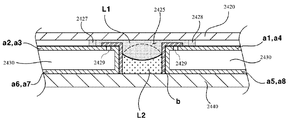
- the liquid lens includes: a first plate having a cavity formed therein for receiving a conductive first liquid and a non-conductive second liquid; A first electrode disposed on the first plate; A second electrode disposed under the first plate; A second plate disposed on the first electrode; And a third plate disposed under the second electrode.
- the second plate and the third plate may be bonded with the holder and the epoxy, respectively.
- At least one of the second plate and the third plate may be spaced apart from the inner surface of the holder.
- the length of the horizontal direction of the first lens unit in the region adjacent to the liquid lens may be greater than the length of the horizontal direction of the cavity in the region adjacent to the first lens unit.
- the length of the second lens unit in the horizontal direction adjacent to the liquid lens may be greater than the length of the cavity in the region adjacent to the second lens unit.
- the first lens unit may include a plurality of lenses, and the holder may have a stepped structure on the inner wall of the first area, and the edge regions of the plurality of lenses may contact the stepped structure.
- the second lens unit may include a plurality of lenses, and the holder may have a stepped structure at an inner wall of the third area, and the edge regions of the plurality of lenses may contact the stepped structure.
- Another embodiment is a holder having an upper and a lower opening and a first hole on the side and a second hole facing the first hole, a first lens unit coupled to the upper portion of the holder, coupled to the lower portion of the holder A second lens unit and a liquid lens disposed between the first lens unit and the second lens unit, the liquid lens being disposed in the first and second holes of the holder and protruding toward the side of the holder.
- At least a camera module including a liquid lens spaced apart from an inner surface of the holder; And a controller converting an image incident through the camera module into an electrical signal.
- a display module including a plurality of pixels whose color is changed by the electrical signal.
- Another embodiment is a step of providing a holder having an upper and a lower opening, the side having a first hole and a second hole facing the first hole; Coupling a first lens unit to an upper portion of the holder; Coupling a second lens unit to a lower portion of the holder; And inserting a liquid lens between the first lens portion and the second lens portion through one of the first and second holes of the holder, wherein the liquid lens is disposed to protrude from the side of the holder.
- a method of manufacturing a camera module including a liquid lens is provided.
- Adjusting the position of the liquid lens by supporting a side of the liquid lens that protrudes from the side of the holder; And bonding the holder and the liquid lens.
- the deposition layers formed on the upper and lower surfaces of the core may be electrically connected to an external power source through the pattern portion formed on the lower surface of the core. Therefore, it has a simple structure compared to the structure of electrically connecting the deposition layer on the upper and lower surfaces of the core with an external power source.
- the space in which the lens assembly and the camera module including the lens assembly are mounted may be reduced.
- the size of the device to be mounted can be effectively reduced.
- the liquid lens unit can be mounted to the base through the insertion hole, the lens assembly can be easily assembled.
- focus alignment may be easily performed in the optical axis direction with respect to the first lens unit of the liquid lens unit mounted to the base through the insertion hole.
- the lenses of the lens module can be aligned by a single core to solve the problem that the optical axis is distorted or shifted.
- the liquid lens since the liquid lens is inserted in the middle of the lens module, the liquid lens may have a compact structure.
- the camera module including the liquid lens according to the embodiment can reduce the size of the camera module by changing the interface between the first and second liquid in the electric, and mechanically moving the lens by performing AF or OIS with the electric It consumes less power and can reduce the size of the camera module.
- the liquid lens can be inserted into the holder and placed stably.
- liquid lens may be inserted after the first lens unit and the second lens unit are disposed in the holder and the optical performance of the first and second lens units is evaluated.
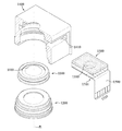
- FIG. 1 is an exploded perspective view showing a lens of an embodiment.
- FIG. 2 is a perspective view of a lens of an embodiment
- FIG. 3 is a side view showing a lens of an embodiment
- FIG. 4 is a schematic cross-sectional view for describing the structure of FIG. 3.
- FIG. 5 is a plan view illustrating a lens of an embodiment.
- FIG. 6 is a bottom view illustrating the lens of one embodiment.
- FIG. 7 and 8 are views for explaining a coupling structure between the lens and the external printed circuit of an embodiment.
- FIG. 9 is a side cross-sectional view illustrating a lens assembly of one embodiment.
- FIG. 10 is an exploded perspective view of FIG. 9.
- FIG. 11 is a perspective view of the camera module of one embodiment.
- FIG. 12 is a diagram illustrating an internal configuration of FIG. 11.
- FIG. 13 is a perspective view showing a camera module provided with a cover member of another embodiment.
- FIG. 14 is a diagram illustrating a state in which the camera module of FIG. 13 is mounted on a device.
- 15 is a conceptual diagram illustrating an electrowetting phenomenon.
- 16 is a perspective view of the camera module of the first embodiment.
- 17 is an exploded perspective view showing the camera module of the first embodiment.
- FIG. 18 is a perspective view showing the shield can of the first embodiment.
- Fig. 19 is a perspective view showing the lens holder of the first embodiment.
- 20 is a sectional view showing the lens holder of the first embodiment.
- 21 is an exploded perspective view showing the liquid lens of the first embodiment.
- Fig. 22 is a plan view showing the liquid lens of the first embodiment.
- 23A to 23L are conceptual cross-sectional views showing that the conductive liquid and the non-conductive liquid are accommodated in the cavity in the first and second embodiments.
- 24 is a sectional view showing the camera module of the first embodiment.
- 25 is an exploded perspective view showing the camera module of the second embodiment.
- Fig. 26 is an exploded perspective view showing the liquid lens of the second embodiment.
- Fig. 27 is a sectional view of the camera module of the second embodiment.
- FIG. 28 is a conceptual diagram illustrating a manufacturing method of the lens module of the first embodiment.
- 29 is a conceptual view illustrating a manufacturing method of the lens module of the second embodiment.
- FIG. 30 is a flow chart showing a manufacturing method of the lens module of the first and second embodiments.
- 31 is a view showing an embodiment of a camera module
- 32A and 32B are views illustrating a liquid lens of the camera module of FIG. 31;
- 33 and 34 are cross-sectional views of the lens assembly of the camera module of FIG. 31;
- 35 is a view illustrating a structure of a lens assembly of the camera module of FIGS. 33 and 34 except for a liquid lens.
- a camera module according to a first embodiment of the present invention, a holder having a first side having a first hole and a second side having a second hole facing the first hole, a first lens disposed in the holder A second lens portion disposed in the holder and a liquid lens disposed between the first lens portion and the second lens portion, and at least partially disposed in the first and second holes of the holder; Based on the optical axis direction, the thickness of the liquid lens may be smaller than the size of the first hole of the holder.
- optical axis direction used below is defined as the optical axis direction of the lens module of the camera module. Meanwhile, the “optical axis direction” may be mixed with the up and down direction, the z axis direction and the like.
- auto focus function used below is defined as a function of focusing on a subject by changing the curvature of the interface of the liquid lens. Meanwhile, “autofocus” may be used interchangeably with “AF (Auto Focus)”.
- shake stabilizer function used below is defined as the function of changing the curvature of the interface of a liquid lens so as to cancel the vibration (movement) which arises in an image sensor by an external force.
- image stabilization may be mixed with "OIS (Optical Image Stabilization)”.
- the lens of the embodiment may include a core 100, an upper glass 200, a lower glass 300, a liquid lens unit 400, and an insulating layer 500.
- the upper glass 200 may be coupled to the upper side of the core 100 to serve to protect the core 100.
- the upper glass 200 may serve to prevent external leakage of the liquid of the liquid lens unit 400 provided in the core 100.
- the lower glass 300 may be coupled to the lower side of the core 100 to serve to protect the core 100.
- the lower glass 300, together with the upper glass 200, may serve to prevent external leakage of the liquid of the liquid lens unit 400 provided in the core 100.
- the upper glass 200 and the lower glass 300 may be formed of a transparent solid material.
- it may be formed of a transparent glass, plastic material.
- Light may be incident on the upper glass 200 to penetrate the core 100 and the lower glass 300 to enter an image sensor (not shown).
- light may be incident on the lower glass 300 to penetrate the core 100 and the upper glass 200 to enter an image sensor (not shown).
- the liquid of the liquid lens unit 400 may be at least partially disposed in the hollow 120 formed in the optical axis direction in the core 100.
- the liquid may be provided with a plurality of liquids that are not mixed with each other, and the shape, curvature, and the like of the boundary surface of each liquid are changed, such that the camera module including the lens performs an autofocusing function and a camera shake correction function. Do it.
- a detailed structure of the liquid lens will be described below with reference to the drawings.
- the core 100 may be disposed between the upper glass 200 and the lower glass 300, and may include an electrode layer 110, a hollow 120, a through hole 130, and a pattern unit 140.
- the electrode layer 110 may be disposed on the core 100 and deposited on the core 100 to form a thin film, and may be formed of a conductive material.
- the electrode layer 110 may be deposited on the core 100 by chemical vapor deposition, plasma vacuum deposition, or other methods.
- the hollow 120 may be formed through the core 100.
- the hollow 120 may be provided with at least a portion of the liquid lens unit 400, and the light passing through the upper glass 200 or the lower glass 300 passes through the core 100.
- at least a part of the electrode layer 110 may be formed to extend into the hollow 120 of the core 100.
- the through hole 130 may be formed through the core 100, and the electrode layer 110 electrically connected to the electrode layer 110 deposited on the upper surface of the core 100 may be extended. .
- the through hole 130 may be deposited on the surface of the through hole 130 so as to be electrically connected to the electrode layer 110 of the upper surface of the core 100.
- the pattern unit 140 may be formed on the bottom surface of the core 100 and may include a plurality of terminals 143. A detailed structure of the pattern unit 140 will be described below with reference to the drawings.
- FIG. 3 is a side view showing a lens of an embodiment
- 4 is a schematic cross-sectional view for describing the structure of FIG. 3.
- the electrode layer 110 may be deposited and disposed on an upper surface, a lower surface, a surface of the hollow 120, and a surface of the through hole 130 of the core 100.
- each of the deposition layers formed on the top and bottom surfaces of the core 100 may be connected to each other by a deposition layer formed on the surface of the through hole 130. That is, the electrode layers 110 disposed on the top and bottom surfaces of the core 100 may be connected to each other by the through hole 130.
- the liquid lens unit 400 may include a first liquid layer 410 and a second liquid layer 420.
- the first liquid layer 410 is provided with a conductive liquid and may be electrically connected to the electrode layer 110.
- the second liquid layer 420 may be provided as a non-conductive liquid and may be disposed to form a boundary with the first liquid layer 410. In this case, at least a portion of the first liquid layer 410 and the second liquid layer 420 may be filled and disposed in the hollow 120.
- first liquid layer 410 and the second liquid layer 420 may form a boundary with each other without mixing.
- the first liquid layer 410 may be electrically connected to the electrode layer 110 to receive current from an external power source through the electrode layer 110.
- the boundary between the first liquid layer 410 and the second liquid layer 420 may be changed in shape, curvature, and the like.
- the camera module provided with the lens of the embodiment can perform the autofocusing function, image stabilization function.
- the insulating layer 500 may be disposed between the electrode layer 110 and the second liquid layer 420. Specifically, as shown in FIG. 4, the insulating layer 500 may be formed on a portion of the upper surface of the core 100, a surface of the hollow 120, and a portion of the upper surface of the lower glass 300. In this case, the insulating layer 500 may be formed by being stacked on the surface of the electrode layer 110 on the upper surface of the core 100, the surface of the hollow 120.
- the insulating layer 500 may serve to prevent the first liquid layer 410 of a conductive material from being directly connected to the electrode layer 110 formed on the bottom surface of the core 100. To this end, as described above, the insulating layer 500 may be formed by stacking the entire portions in which the first liquid layer 410 is directly and electrically connected to the electrode layer 110 on the bottom surface of the core 100. have.
- the first liquid layer 410 may be electrically connected to the electrode layer 110 on the bottom surface of the core 100 through the through hole 130.
- the core 100 structure of the embodiment illustrated in FIG. 4 may be formed by, for example, the following procedure.
- the hollow 120 and the through hole 130 are formed in the core 100.
- the electrode layer 110 is deposited on the upper surface, the lower surface, the hollow 120 and the through hole 130 surface of the core 100.
- the pattern unit 140 may be formed on the electrode layer 110 deposited on the bottom surface of the core 100.
- the lower glass 300 is bonded to the lower surface of the core 100 by fusion or the like.
- an insulating film is laminated on the core 100.
- a liquid is injected into the core 100 to form a liquid lens unit 400 including a first liquid layer 410 and a second liquid layer 420.
- the upper glass 200 is coupled to the upper surface of the core 100 by fusion or the like to complete the assembly of the core 100.
- a voltage or a current must be applied, and when the electrode layer 110 on the upper surface of the core 100 and the electrode layer 110 on the lower surface are not electrically connected to each other, the lens is used for electrical connection with an external power source.
- a separate connector or the like should be separately connected to each electrode layer 110 of the upper and lower surfaces of the core 100.
- FIGS. 5 and 6 are plan views showing a lens of an embodiment. 6 is a bottom view illustrating the lens of one embodiment. As shown in FIGS. 5 and 6, the through-hole 130 having the electrode layer 110 formed on the surface of the electrode layer 110 on the upper surface of the core 100 and the pattern portion 140 on the lower surface of the core 100 is formed. Can be electrically connected
- FIG. 4 may correspond to a view showing a cross section along a cutting line A-A 'shown in FIG. 6.
- the pattern unit 140 may be formed by, for example, depositing the electrode layer 110. That is, the pattern layer 140 may be formed by patterning the electrode layer 110 deposited on the lower surface of the core 100 by etching or the like.
- the pattern portion 140 is formed such that the plurality of terminals 143 are electrically separated from each other, and at least one of the plurality of terminals 143 is disposed on an upper surface of the core 100. It may be electrically connected to the electrode layer 110 and the through hole 130 to be deposited.
- the plurality of terminals 143 may be connected to both the upper and lower electrode layers 110 of the core 100.
- at least some of the plurality of terminals 143 may be electrically connected to the first liquid layer 410 through the electrode layer 110 on the upper surface of the core 100.
- the pattern part 140 may include a first pattern part 141 and a second pattern part 142.
- the first pattern portion 141 is a portion that is coupled to the lower glass 300
- the second pattern portion 142 is a portion provided to be exposed to one side of the lower glass 300.
- the second pattern part 142 may be electrically connected to the external printed circuit board 10. Therefore, the second pattern portion 142 is aligned at regular intervals to facilitate connection with the external printed circuit board 10, and is provided as a portion of the plurality of terminals 143 having the same or similar shape to each other. Can be.
- the plurality of terminals 143 may include a first terminal 143a.
- the first terminal 143a may include the electrode layer 110 formed on an upper surface of the core 100 and the electrode layer 110 formed in the through hole 130. And can be electrically connected.
- the electrode layer 110 on the upper surface of the core 100 may be disposed in a circular shape on the upper surface of the core 100 around the hollow 120.
- the electrode layer 110 on the upper surface of the core 100 is integrally connected and connected to the first terminal 143a through the electrode layer 110 formed in the through hole 130 to receive the same current from an external power source. Can be.
- the electrode layer 110 connected to the first terminal 143a may be defined as a common electrode.
- the remaining terminals 143 except for the first terminal 143a may be electrically connected to the electrode layer 110 dividing the periphery of the hollow 120 into four regions of the pattern portion 140 on the bottom surface of the core 100. have.
- the electrode layers 110 corresponding to the four regions may be disposed under the insulating layer 500 along the inclined surface of the hollow 120, respectively.
- the electrode layers 110 corresponding to the four regions may receive current through the remaining terminals 143 except for the first terminal 143a.
- the electrode layer 110 connected to the remaining terminals 143 except for the first terminal 143a may be defined as individual electrodes.
- the current is applied from the external power source by the terminals 143 including the first terminal 143a, so that the shape of the curvature boundary of the boundary formed by the first liquid layer 410 and the second liquid layer 420 is formed. , Curvature, etc. may be changed.
- the camera module including the lens may perform an autofocusing function and a camera shake correction function.
- FIG. 7 and 8 are views for explaining a coupling structure between the lens and the external printed circuit of an embodiment.
- the plurality of terminals 143 formed in the pattern unit 140 are external printed circuits in the second pattern unit 142 provided to be exposed at one side of the lower glass 300. It may be electrically connected to the substrate 10.
- the external printed circuit board 10 may have external terminals 11 formed at both ends, one end of the external terminals 11 may be electrically connected to the lens, and the other end may be electrically connected to an external power source. Can be.
- the terminals 143 may be electrically coupled to the external terminal 11 of the external printed circuit board 10.
- the terminals 143 and the external terminals 11 may be coupled and electrically connected by soldering, fusion, a conductive film or an adhesive, and the like.
- the deposition layer formed on the upper and lower surfaces of the core 100 may be electrically connected to an external power source only in the pattern unit 140 formed on the lower surface of the core 100. Therefore, the structure has a simpler structure than the structure for electrically connecting the deposition layers on the upper and lower surfaces of the core 100 to an external power source.
- the configuration of the lens and the camera module including the same can be simplified and downsized, thereby reducing the manufacturing time, effort, and cost of the lens and the camera module including the same.
- the camera module including the lens may further include an image sensor (not shown).
- the image sensor may be provided to face the lens in the optical axis direction.
- the image sensor may form an image of a subject.
- an infrared cut filter may be provided between the lens and the image sensor so as to face the lens and the image sensor in the optical axis direction.
- the infrared cut filter may play a role of increasing the image quality of the image formed on the image sensor.
- the lens assembly may include a first lens unit 1100, a second lens unit 1200, a liquid lens unit 1300, a base 1400, a printed circuit board 1500, and a cover member 1600. .
- the first lens unit 1100 is disposed in front of the lens assembly and is a portion where light is incident from the outside of the lens assembly.
- the first lens unit 1100 may be provided with at least one lens, or two or more lenses may be aligned in the optical axis direction to form an optical system.
- the first lens unit 1100 may be mounted on the base 1400.
- a through hole may be formed in the base 1400, and the first lens unit 1100 may be disposed in the through hole.
- the first lens unit 1100 may include an exposure lens 1110.
- the exposure lens 1110 is a lens protruding out of the base 1400 and exposed to the outside. In the case of the exposure lens 1110, the lens surface is likely to be damaged due to exposure to the outside.
- the lens surface is damaged, the image quality of the image photographed by the camera module may be degraded. Therefore, measures for preventing and suppressing surface damage of the exposure lens 1110 are necessary.
- a cover glass may be disposed in front of the exposure lens 1110 to prevent surface damage of the exposure lens 1110.
- the space in which the lens assembly and the camera module including the same is mounted becomes wider, and thus the size of the device on which the lens assembly and the camera module are mounted may be increased.
- a structure for preventing and suppressing surface damage of the exposure lens 1110 without using a cover glass is disclosed.
- the exposure lens 1110 may be formed of at least a portion of an abrasion resistant material, for example, a glass material.
- the entire exposed lens 1110 may be formed of a glass material having high wear resistance.
- the effect of preventing and suppressing surface damage is significantly higher than that of the plastic exposure lens 1110.
- the exposure lens 1110 may form a wear resistant coating layer on the external exposed portion.
- the wear resistant coating layer may be, for example, a diamond like carbon (DLC) coating layer.
- DLC diamond like carbon
- DLC coating is to deposit a coating layer on the surface of the object by using carbon gas, which is a main component of diamond, the deposited coating layer may have a structure and properties similar to diamond.
- the exposed lens 1110 having the DLC coating layer may have high wear resistance.
- the space in which the lens assembly and the camera module including the lens assembly are mounted may be reduced.
- the size of the device on which the module is mounted can be effectively reduced.
- the second lens unit 1200 is disposed behind the first lens unit 1100 and the liquid lens unit 1300, and light incident from the outside into the first lens unit 1100 is transferred to the liquid lens unit 1300. The light may pass through and enter the second lens unit 1200.
- the second lens unit 1200 may be disposed in a through hole formed in the base 1400 spaced apart from the first lens unit 1100.
- the second lens unit 1200 may be provided with at least one lens, or two or more lenses may be aligned in the optical axis direction to form an optical system.
- the second lens unit 1200 may be mounted on the base 1400.
- the liquid lens unit 1300 may be disposed between the first lens unit 1100 and the second lens unit 1200 and may be mounted on the base 1400.
- the liquid lens unit 1300 may have a hollow 1310 in the optical axis direction.
- the hollow 1310 is a portion through which the light passing through the first lens unit 1100 is transmitted, and at least a portion of the hollow 1310 may be filled with liquid.
- the hollow 1310 may be provided such that an optical axis area decreases toward the second lens unit 1200 from the first lens unit 1100.
- the hollow 1310 may be filled with, for example, two kinds of conductive liquids and a non-conductive liquid, and the conductive liquid and the non-conductive liquid may form an interface without mixing with each other.
- the interface when the conductive liquid is electrically connected to an external power source and a current is applied from the external power source, the interface may be deformed or the curvature may be changed.
- the liquid lens unit 1300, the lens assembly and the camera module including the same may perform an autofocusing function, a camera shake correction function, and the like.
- the first lens unit 1100, the second lens unit 1200, and the liquid lens unit 1300 may be disposed to face each other in the optical axis direction.
- the first lens unit 1100, the second lens unit 1200, and the liquid lens unit 1300 may be aligned with each other in the optical axis direction. .
- the respective focal points are aligned with each other in the optical axis direction.
- the focal points of the first lens unit 1100, the second lens unit 1200, and the liquid lens unit 1300 are aligned in the optical axis direction.
- it may mean that they must be located on the same line as each other or at least within the designed range.
- each lens unit may be regarded as aligned with each other in the optical axis direction only when positioned in the virtual line PL or outside the design line even if it is outside the virtual line PL.
- the focal points of each lens unit are disposed at positions outside the design range, the image quality of the photographed image may be degraded, and thus a structure for aligning these focal points is necessary.
- This may be implemented by the structure of the base 1400 proposed in the embodiment.
- the structure of the base 1400 of the embodiment will be described in detail.
- the first lens unit 1100, the second lens unit 1200, and the liquid lens unit 1300 may be mounted on the base 1400 so as to face each other in the optical axis direction.
- a space penetrating in the optical axis direction may be formed in the base 1400 to mount the lens units, and the lens units may be disposed in the space.
- the base 1400 may include an insertion hole 1410 into which the liquid lens unit 1300 is inserted. That is, the base 1400 may have an insertion hole 1410 into which the liquid lens unit 1300 is inserted.
- the insertion hole 1410 may be formed at one side of the base 1400 to communicate with an internal space of the base 1400, as shown in FIG. 9 and FIG. 10 described below.
- the liquid lens unit 1300 may have a larger optical axis area than that of the first lens unit 1100 or the second lens unit 1200.
- the optical axis direction of the hollow 1310 filled with liquid may be smaller than that of the first lens unit 1100 or the second lens unit 1200, and the liquid lens unit 1300.
- the overall optical axis area is reduced, the area of the hollow 1310 is smaller, and the light transmitting area of the light passing through the liquid lens unit 1300 is smaller.
- the amount of light transmitted decreases, which may significantly reduce the brightness of the image. Therefore, there is a limitation in reducing the light transmission area of the liquid lens unit 1300 and thus the optical axis direction area of the hollow 1310.
- the optical axis direction area of the liquid lens unit 1300 may be formed larger than the optical axis direction area of the first lens unit 1100 or the second lens unit 1200. Accordingly, the liquid lens unit 1300, like the first lens unit 1100 or the second lens unit 1200, moves upward from the open bottom of the space of the base 1400 to the upper direction of the base 1400. It is difficult to mount on the base 1400.
- the liquid lens unit 1300 may be mounted on the base 1400 through the insertion hole 1410, the lens assembly may be easily assembled.
- the printed circuit board 1500 coupled with the liquid lens unit 1300 may also be easily mounted on the base 1400.
- focus alignment may be easily performed in the optical axis direction with respect to the first lens unit 1100 of the liquid lens unit 1300 mounted to the base 1400 through the insertion hole 1410.
- the printed circuit board 1500 may be electrically connected to the liquid lens unit 1300, and at least a part of the printed circuit board 1500 may be inserted into the insertion hole 1410.
- the printed circuit board 1500 may have terminals 1510 at both ends thereof, and may be provided in a bent form so as to be embedded in the cover member 1600.
- terminals 1510 provided at one end thereof are coupled to the liquid lens unit 1300 to be electrically connected to the liquid lens unit 1300, and terminals 1510 provided at the other end thereof may be connected to the liquid lens unit 1300. Can be electrically connected to an external power source.
- the terminals 1510 provided at the other end may be electrically connected to the sensor holder 1010. A structure related thereto will be described in detail below.
- FIG. 10 is an exploded perspective view of FIG. 9. A method of assembling the lens assembly and the method of focusing alignment of the lens parts of the embodiment will be described with reference to FIG. 10.
- the first lens unit 1100 is mounted on the base 1400.
- the first lens unit 1100 may be disposed in the inner space of the base 1400 through an opening formed in the lower portion of the base 1400.
- the focus of the first lens unit 1100 may be located on the virtual line PL.
- the first lens unit 1100 When the first lens unit 1100 is disposed at a position designed in the inner space of the base 1400, the first lens unit 1100 is coupled to the base 1400 using an adhesive or the like.
- the liquid lens unit 1300 is mounted on the base 1400.
- the liquid lens unit 1300, to which the printed circuit board 1500 is coupled, may be disposed in the inner space of the base 1400 through the insertion hole 1410.
- the liquid lens unit 1300 may be moved in a direction perpendicular to the optical axis direction to align the focus of the first lens unit 1100 with the focus of the liquid lens unit 1300 in the optical axis direction. have.
- the liquid lens unit 1300 is disposed in the interior space of the base 1400, and the liquid lens unit 1300 is coupled to the base 1400 using an adhesive or the like.
- the second lens unit 1200 is mounted on the base 1400.
- the second lens unit 1200 may be disposed in the inner space of the base 1400 through an opening formed in the lower portion of the base 1400.
- the second lens unit 1200 is moved in a direction perpendicular to the optical axis direction to focus the second lens unit 1200, the first lens unit 1100, and the liquid lens unit 1300 in the optical axis direction. Can be aligned with each other.
- the second lens unit 1200 is disposed in the interior space of the base 1400, and couples the second lens unit 1200 to the base 1400 using an adhesive or the like. .
- the liquid lens unit 1300 may be arranged such that the focal point is aligned in the optical axis direction with respect to the first lens unit 1100.
- the second lens unit 1200 may be disposed so that the focal point is aligned in the optical axis direction with respect to the first lens unit 1100 and the liquid lens unit 1300.
- the first lens unit 1100, the second lens unit 1200, and the liquid lens unit 1300, which are disposed and mounted on the base 1400, may be aligned with each other in the optical axis direction. Can be.
- the optical axis direction area of the hollow 1310 formed in the liquid lens part 1300 is smaller than the optical axis direction area of the lens forming the first lens part 1100 or the second lens part 1200. Can be.
- the lenses forming the first lens unit 1100 and the second lens unit 1200 are lenses having a structure in which light can be incident on the entire optical axis area, but in the liquid lens unit 1300, the hollow 1310. This is because it is appropriate to form an area of the hollow 1310 smaller than that of the first lens unit 1100 or the second lens unit 1200 in order to miniaturize the lens assembly.
- the amount of light passing through the hollow 1310 may be smaller. Therefore, when the liquid lens unit 1300 is disposed in front of the first lens unit 1100, the arrangement of the embodiment, that is, the liquid lens unit 1300, the first lens unit 1100 and the second lens unit The amount of light incident on the lens assembly is smaller than that of the case where the pixels are disposed between 1200, and thus, the image quality of the captured image may be deteriorated.
- the viewing angle of the camera module due to the hollow 1310 has a small area (view angle) can be narrowed.
- the hollow 1310 of the liquid lens unit 1300 may be disposed.
- the transmitted light may be refracted while passing through the second lens unit 1200 having a large area, and thus may have a wider viewing angle than when the liquid lens unit 1300 is disposed behind the second lens unit 1200.
- the viewing angle does not decrease and the amount of light that is incident does not decrease.
- the lens assembly can be implemented.
- FIG. 11 is a perspective view of the camera module of one embodiment.
- 12 is a diagram illustrating an internal configuration of FIG. 11. As illustrated in FIGS. 11 and 12, the lens assembly of the embodiment may further include a cover member 1600.
- the cover member 1600 may accommodate the base 1400 and the printed circuit board 1500, and thus, the first lens unit 1100 and the second lens unit 1200 may be mounted on the base 1400. And a liquid lens unit 1300 to serve to protect these lens units.
- the cover member 1600 may be provided in a form in which a hollow is formed and a lower portion thereof is opened, and a through hole through which the front portion of the first lens unit 1100 is exposed.
- the camera module of the embodiment may include the lens assembly, the image sensor 1011, and the sensor holder 1010 having the above-described structure.
- the image sensor 1011 is disposed to face the lens assembly in the optical axis direction, and light sequentially passing through the first lens unit 1100, the liquid lens unit 1300, and the second lens unit 1200 is incident to the lens assembly. This is where the image is taken.
- a filter may be provided between the second lens unit 1200 and the image sensor 1011 to increase the quality of the captured image, and the filter may be, for example, an infrared cut filter. .
- the sensor holder 1010 may be mounted or mounted on the image sensor 1011 and may be coupled to the base 1400. In addition, the sensor holder 1010 may be equipped with various elements for the operation of the entire camera module. In addition, the sensor holder 1010 may be electrically connected to the printed circuit board 1500.
- connection part (not shown) electrically connected to the terminal 1510 formed on the printed circuit board 1500 may be formed in the sensor holder 1010, and the terminal 1510 and the connection part are soldered, It may be bonded to each other with a conductive adhesive or the like.
- the sensor holder 1010 may be provided with a connector 1012 for connection with an external power source.
- the siye liquid lens unit 1300 may be electrically connected to an external power source through the printed circuit board 1500, the sensor holder 1010, and the connector 1012, and may be driven by receiving a current from the external power source.
- FIG. 13 is a perspective view illustrating a camera module provided with a cover member 1600 according to another embodiment.
- 14 is a diagram illustrating a state in which the camera module of FIG. 13 is mounted on a device.
- the cover member 1600 may have a protruding core 1610 formed therein.
- the protruding core 1610 may be provided in a form in which the periphery of the hole formed in the cover member 1600 protrudes in the optical axis direction so that the exposed portion of the first lens unit 1100, that is, the exposure lens 1110 is exposed to the outside. Can be.
- the base 1400 may be formed in a shape in which the front portion protrudes corresponding to the shape of the protruding core 1610. As shown in FIG. 13, a space may be formed inside the protruding core 1610, and a first lens unit 1100 may be mounted in the space.
- the protruding core 1610 may be inserted into an opening formed in the cover 1020 of the device. Due to this structure, compared to the structure of the lens assembly described in Figures 9 to 12, the lens assembly of the embodiment does not reduce the overall length of the optical axis direction of the lens assembly without changing the shape of the cover member 600 and thus the base 1400 By changing the shape, it is possible to reduce the space occupied by the lens assembly and the camera module including the same in the device.
- the base 1400 and the through hole described in FIGS. 9 to 14 may be differently defined as holders and through holes, respectively.
- the insertion hole 1410 is composed of two holes facing each other, the insertion hole 1410 may be differently defined as the first hole and the second hole.
- the optical device may be a mobile phone, a mobile phone, a smart phone, a portable smart device, a digital camera, a laptop computer, a digital broadcasting terminal, a personal digital assistant (PDA), a portable multimedia player (PMP), navigation, or the like.
- PDA personal digital assistant
- PMP portable multimedia player
- the present invention is not limited thereto, and any device for taking an image or a picture may be used.
- the optical apparatus may include a main body (not shown), a display unit (not shown), and camera modules 2000 and 2001.
- the body may form the appearance of the optical device.
- the main body may include a cuboid shape as an example. However, it is not limited thereto. As a variant, the body may be formed round at least in part.
- the main body may accommodate the camera modules 2000 and 2001.
- the display unit may be disposed on one surface of the main body.
- the camera modules 2000 and 2001 may be disposed in the main body.
- the camera modules 2000 and 2001 may be disposed on one surface of the main body. At least a part of the camera modules 2000 and 2001 may be accommodated in the main body.
- the camera modules 2000 and 2001 may photograph an image of a subject.
- the display unit may be disposed in the main body.
- the display unit may be disposed on one surface of the main body. That is, the display unit may be disposed on the same surface as the camera modules 2000 and 2001. Alternatively, the display unit may be disposed on a surface different from one surface of the main body.
- the display unit may be disposed on a surface that is opposite to the surface on which the camera modules 2000 and 2001 are disposed.
- the display unit may output an image photographed by the camera modules 2000 and 2001.
- FIG. 16 is a perspective view showing the camera module of the first and second embodiments
- FIG. 17 is an exploded perspective view showing the camera module of the first embodiment
- FIG. 18 is a perspective view showing the shield can of the first embodiment
- FIG. 19. 20 is a perspective view showing the lens holder of the first embodiment
- FIG. 20 is a sectional view showing the lens holder of the first embodiment
- FIG. 21 is an exploded perspective view showing a liquid lens of the first embodiment
- FIG. 22 is a first view.
- 23A to 23L are conceptual cross-sectional views showing that the conductive liquid and the non-conductive liquid are accommodated in the cavity in the first and second embodiments
- FIG. 24 shows the camera module of the first embodiment. It is sectional drawing shown.
- the camera module 2000 of the first embodiment may be an AF driving camera module.
- the camera module 2000 may be referred to as an “AF camera module”.
- the camera module 2000 may be provided as an OIS driving camera module.
- the camera module 2000 may include a cover member 2100, a lens module, an infrared filter 2600, a main board 2700, an image sensor (not shown), and a controller (not shown). However, at least one of the cover member 2100, the infrared filter 2600, the main board 2700, and the image sensor (not shown) may be omitted or changed in the camera module 2000.
- the cover member 2100 may form an appearance of the camera module 2000.
- the cover member 2100 may have a hexahedron shape of which a lower portion is opened. However, it is not limited thereto.
- the cover member 2100 may be a nonmagnetic material.
- the cover member 2100 may be provided with a metal plate.
- the cover member 2100 may block electro magnetic interference (EMI). Because of this feature of cover member 2100, cover member 2100 may be referred to as an "EMI shield can.”
- the cover member 2100 may block radio waves generated from the outside of the camera module 2000 from flowing into the cover member 2100.
- the cover member 2100 may block radio waves generated inside the cover member 2100 from being emitted to the outside of the cover member 2100.
- the material of the cover member 2100 is not limited to the metal plate.
- the cover member 2100 may include an upper plate 2120 and a plurality of side plates 2130.
- the cover member 2100 may include a plurality of side plates 2130 extending downward from the outside of the upper plate 2120 and the upper plate 2120.
- the cover member 2100 may be located on an outer surface of the lens holder 2200.
- the cover member 2100 may be in contact with the outer surface of the lens holder 2200.
- Lower ends of the various side plates 2130 of the cover member 2100 may be mounted on the lens holder 2200.
- Lower ends of the side plates 2130 of the cover member 2100 may be mounted on the stepped portion 2250 of the lower portion of the lens holder 2200.
- the upper plate 2120 may have a plate shape. Each side of the upper plate 2120 may have a plurality of side plates 2130 extending downward. In this case, the top plate 2120 and the plurality of side plates 2130 may be integrally formed.
- the first transmission window 2110 may be located at the center of the upper plate 2120.
- the first transmission window 2110 is a circular hole formed in the center of the upper plate 2120 and may be centered on the optical axis of the lens module described later. Accordingly, the light reflected from the subject may be irradiated to the lens module through the first transmission window 2110.
- the side plate 2130 may extend downward from each of four sides of the top plate 2120. As a result, the total number of side plates 2130 may be four. Furthermore, each side plate 2130 may be spaced apart from each other. The lower end of the side plate 2130 may be mounted on the stepped portion 2250 of the lower portion of the lens holder 2200.
- the slit 2140 may be a space in which the plurality of side plates 2130 are spaced apart from each other. That is, the slit 2140 may be located between neighboring side plates 2130 of the plurality of side plates 2130. The slit 2140 may be located along four vertical sides of the cover member 2100.
- the slit 2140 may include first, second, and third gaps 2142, 2144, and 2146.
- the first gap 2142 may be formed along the vertical side of the cover member 2100.
- the second and third gaps 2144 and 2146 may be formed by splitting an upper end of the first gap 2142 from both upper edges of the cover member 2100. Upper ends of the second and third gaps 2144 and 2146 may be rounded.
- the cover member 2100 after forming the cover member 2100 in the form of an unfolded flat plate by forming an integrated flat plate, the cover member 2100 can be completed by folding several side plates 2130 downward. In this case, since the upper ends of the second and third gaps 2144 and 2146 are rounded, the side plates 2130 can be easily folded. Furthermore, it is possible to prevent the stress from being concentrated at both ends of the portion where the side plate 2130 is folded, thereby preventing cracks from occurring.
- the lens module may include a lens holder 2200, a first lens unit 2300, a liquid lens 2400, and a second lens unit 2500.
- the main substrate 2700 may be located under the lens module.
- the lens module may be supported by the main substrate 2700.
- the lower end of the lens module may be mounted on the main substrate 2700.
- the lower end of the lens module may be mounted outside the upper surface of the main board 2700.
- the light transmitted through the lens module may be irradiated to the image sensor mounted inside the upper surface of the main substrate 2700.
- the lens module may include a base plate.
- the lower end of the lens module may be mounted and supported on the base plate.
- the main substrate may be located under the base plate.
- the base plate may be mounted outside the upper surface of the main board.
- the lens holder 2200 may be a plastic injection molded block.
- the lens holder 2200 may be manufactured by hole molding.
- a hole 2210 may be formed in the center of the lens holder 2200 in the optical axis direction.
- the lens holder 2200 may have a hole 2210 penetrating the center portion of the lens holder 2200 in the optical axis direction.
- the hole 2210 may be located in the lens holder 2200.
- the hole 2210 may be positioned in the optical axis direction at the center of the lens holder 2200.
- the hole 2210 may be formed in the optical axis direction at the center of the lens holder 2200.
- the hole 2210 may be formed by penetrating the lens holder 2200 in the vertical direction. Therefore, the upper and lower sides of the lens holder 2200 may be opened by the holes 2210.
- the first lens unit 2300, the liquid lens 2400, and the second lens unit 2500 may be accommodated in the hole 2210.
- the hole 2210 may include a second transmission window 2211, a first lens accommodation hole 2220, a second lens accommodation hole 2230, an insertion hole 2232, and a third lens accommodation hole 2240. .
- the second transmission window 2211, the first lens accommodation hole 2220, the second lens accommodation hole 2230, and the third lens accommodation hole 2240 may be sequentially disposed from the upper side to the downward direction. have.
- the first lens part 2300, the liquid lens 2400, and the second lens part 2500 may be sequentially received from the image side to the downward direction. In this case, the optical axes of the first lens unit 2300, the liquid lens 2400, and the second lens unit 2500 may be aligned.
- the second transmission window 2211 may be located at the uppermost side of the hole 2210.
- the second transmission window 2211 may be circular.
- the first transmission window 2110 may be spaced vertically apart from the second transmission window 2211.
- the first lens accommodation hole 2220 may be positioned below the second transmission window 2211.
- the second transmission window 2211 and the first lens receiving hole 2220 may communicate in the vertical direction.
- the second transmission window 2211 may be integrally formed with the first lens accommodation hole 2220. That is, the second transmission window 2211 may be part of the first lens accommodation hole 2220. In this case, the uppermost lens of the first lens unit 2200 may protrude through the second transmission window 2211.
- the first lens accommodation hole 2220 may be located at the center of the hole 2210.
- the second transmission window 2211 may be positioned on an image side of the first lens accommodation hole 2220.
- the second lens accommodation hole 2230 may be positioned below the first lens accommodation hole 2220.
- the second transmission window 2211, the first lens accommodation hole 2220, and the second lens accommodation hole 2230 may communicate in the vertical direction.
- the second transmission window 2211, the first lens accommodation hole 2220, and the second lens accommodation hole 2230 may be aligned in the optical axis direction.
- the first lens unit 2300 may be accommodated in the first lens accommodation hole 2220.
- the second lens accommodation hole 2230 may be located in the middle of the hole 2210.
- the first lens accommodation hole 2220 may be positioned on an image side of the second lens accommodation hole 2230.
- the third lens accommodation hole 2240 may be positioned below the second lens accommodation hole 2230.
- the first lens accommodation hole 2220, the second lens accommodation hole 2230, and the third lens accommodation hole 2240 may communicate with each other in the vertical direction.
- the first lens accommodation hole 2220, the second lens accommodation hole 2230, and the third lens accommodation hole 2240 may be aligned in the optical axis direction.
- the liquid lens 2400 may be accommodated in the second lens accommodation hole 2230. As a result, the optical axes of the first lens unit 2300 and the liquid lens 2400 may be aligned.
- the insertion hole 2232 may be formed on the side of the lens holder 2200.
- the insertion hole 2232 may be formed in a direction inclined to the optical axis direction in the lens holder 2200.
- the insertion hole 2232 may be formed in an inclined shape and an optical axis direction from the surface of the lens holder 2200 to the hole 2210.
- the insertion hole 2232 may be formed perpendicular to the optical axis direction from the surface of the lens holder 2200 to the hole 2210.
- the insertion hole 2232 may be formed to be inclined with the optical axis direction through one side of the lens holder 2200.
- the insertion hole 2232 may pass through one side surface of the lens holder 2200 and be perpendicular to the optical axis direction.
- a part of one side of the lens holder 2200 may be opened by the insertion hole 2232.
- the insertion hole 2232 may communicate with the hole 2210.
- the insertion hole 2232 may be in communication with the second lens accommodation hole 2230.
- the liquid lens 2400 may be inserted in the side of the lens holder 2200 through the insertion hole 2232 and accommodated in the second lens accommodation hole 2230.
- a substrate accommodation groove 2234 extending downward may be formed in communication with the insertion hole 2232.
- the upper receiving substrate 2410b and the lower connecting substrate 2450b to be described later may be accommodated in the substrate receiving groove 2234.
- the substrate receiving groove 2234 may extend to the lower end of the lens holder 2200. Since the upper connecting board 2410b and the lower connecting board 2450b are positioned along the board receiving groove 2234, the upper connecting board 2410b and the lower connecting board 2450b may be electrically connected to the main board 2700 located under the lens holder 2200.
- the third lens accommodation hole 2240 may be disposed in the hole 2210.
- the second lens accommodation hole 2230 may be positioned on an image side of the third lens accommodation hole 2240.
- the second lens accommodation hole 2230 and the third lens accommodation hole 2240 may communicate in the vertical direction.
- the second lens accommodation hole 2230 and the third lens accommodation hole 2240 may be aligned in the optical axis direction.
- the second lens unit 2500 may be accommodated in the third lens accommodation hole 2240. As a result, the optical axes of the liquid lens 2400 and the second lens unit 2500 may be aligned.
- the liquid lens 2400 is larger in size than the other lenses. Therefore, when the liquid lens 2400 is inserted through the lower opening of the hole 2210, an upper hole accommodating the first lens part 2300 and the liquid lens 2400 and a lower side accommodating the second lens part 2500 are provided. Each hole is required. Since each hole is formed by a separate hole forming process, problems may arise in that optical axes of the upper and lower holes do not coincide with each other. However, in the first embodiment, the liquid lens 2400 is inserted from the side by the insertion hole 2232. As a result, both the first lens unit 2300, the liquid lens 2400, and the second lens unit 2500 may be accommodated in one hole 2210. That is, since all the lenses are accommodated in the hole 2210 integrally formed by a single hole forming process, the optical axis is not twisted.
- the first lens unit 2300 may include one or more lenses.
- the first lens unit 2300 may include two lenses.
- the lenses of the first lens unit 2300 may be positioned in a stacked form.
- the first lens unit 2300 may be accommodated in the first lens accommodation hole 2220.
- the lenses of the first lens unit 2300 may have an upper portion of the lens contacting the step or the O-ring of the first lens accommodation hole 2220, and a lower portion of the lens may be supported by the lower lens or the O-ring.
- a lower portion of the lowermost lens of the first lens unit 2300 may contact the upper surface of the upper plate 2420 of the liquid lens 2400, which will be described later.
- a lower portion of the lowermost lens of the first lens unit 2300 may be supported and fixed on the upper surface of the upper plate 2420 of the liquid lens 2400, which will be described later.
- An inclined portion 2310 may be disposed along the outer circumference of the bottom surface of the lowermost lens of the first lens unit 2300.
- the inclined portion 2310 may be formed to slope down to the inside of the lens holder 2200.
- the liquid lens 2400 is a lens that performs AF and OIS functions by controlling the curvature of the interface between the conductive liquid and the non-conductive liquid.
- the conductive liquid and the non-conductive liquid are accommodated and the electrode and the insulator are stacked to apply a voltage to the electrode, the contact angle of the inner surface of the cavity coated with the conductive liquid and the insulator changes according to the intensity of the applied voltage. ) Phenomenon occurs.
- the electrowetting phenomenon will be described in more detail.
- the conductive droplet 2040 is dropped on the upper surface of the electrically insulated insulating layer 2014, a spherical shape shown in FIG. 15 is formed.
- the upper electrode part includes the first to fourth electrode parts a1, a2, a3, and a4, and the inner wall electrode part is the fifth to eighth. It is assumed that the electrode portions a5, a6, a7, a8 are included.
- the liquid lens 2400 may be located inside the lens holder 2200.
- the liquid lens 2400 may be accommodated in the hole 2210.
- the liquid lens 2400 may be accommodated in the second lens accommodation hole 2230 through the insertion hole 2232.
- the liquid lens 2400 has an upper portion contacting the lower surface of the lowermost lens of the first lens portion 2300 and the upper surface of the second lens accommodation hole 2230, and the lower portion of the liquid lens 2400 upper surface of the uppermost lens of the second lens portion 2500. It may be supported and fixed to the lower surface of the second lens receiving hole (2230).
- the liquid lens 2400 may be inserted in one side of the lens holder 2200 and accommodated in the hole 2210.
- the liquid lens 2400 may be accommodated in the second lens accommodation hole 2230 through the insertion hole 2232.
- the liquid lens 2400 may be electrically connected to the main substrate 2700. The curvature of the interface of the liquid lens 2400 can be controlled.
- the liquid lens 2400 may have a form in which a substrate and a plate are stacked.
- the liquid lens 2400 may include an upper substrate 2410, an upper plate 2420, a core plate 2430, a lower plate 2440, and a lower substrate 2450.
- the upper substrate 2410 may be disposed above the liquid lens 2400.
- An upper plate 2420 may be positioned below the upper substrate 2410.
- An upper plate 2420 may be disposed between the upper substrate 2410 and the core plate 2430.
- An upper surface of the upper substrate 2410 may be in contact with an inner inner wall of the second lens accommodation hole 2230.
- the upper substrate 2410 may be electrically connected to an electrode disposed on the core plate 2430.
- the upper substrate 2410 may be electrically connected to the main substrate 2700.
- the upper substrate 2410 may be controlled by the main substrate 2700 to apply power to the electrode portion a of the core plate 2430, which will be described later.
- the upper substrate 2410 may change the direction, intensity, wavelength, and location where the current is applied to the electrode unit a.
- the upper substrate 2410 may include an upper circuit board 2410a and an upper connection board 2416b.
- the upper circuit board 2410a may be a printed circuit board (PCB).
- the upper circuit board 2410a may have a plate shape.
- the upper circuit board 2410a may have a rectangular plate shape.
- the upper circuit board 2410a includes an upper guide hole 2415 extending to one side from a portion extending radially from a portion corresponding to (or facing) the cavity 2431 or a portion corresponding to (or facing) the cavity 2431 to be described later. This can be formed.
- One side may be a side located at a first entrance in the direction in which the liquid lens 2400 is inserted into the insertion hole 2232. This is to minimize friction between the bottom surface of the lowermost lens of the first lens unit 2300 and the upper circuit board 2410a when the liquid lens 2400 is inserted.
- the bottom surface of the lowermost lens of the first lens unit 2300 may be supported by the upper guide hole 2415 in contact with the upper plate 2420.
- the lens of the pre-inserted first lens unit 2300 may be fixed at a predetermined position without swinging.
- the upper circuit board 2410a may be worn or the upper circuit board 2410a may be detached and detached from the upper plate 2420 or the core plate 2430 by friction generated when the liquid lens 2400 is inserted. Can be.
- the first upper corner part 2411, the second upper corner 2412, the third upper corner part 2413, and the fourth upper corner part 2414 may be positioned in the upper circuit board 2410a in the counterclockwise direction. .
- the first to fourth upper corner parts 2411, 2412, 2413, and 2414 of the upper circuit board 2410a may be positioned inside the corners of the core plate 2430. That is, the corner portion of the upper substrate 2410 may be located inward from the corner portion of the core plate 2430. This is to minimize friction between the first to fourth upper corner portions 2411, 2412, 2413, and 2414 and the inner inner wall and sidewalls of the two lens accommodation holes 2230 when the liquid lens 2400 is inserted.
- the adhesion between the first to fourth upper corner portions 2411, 2412, 2413, and 2414 and the core plate 2430 may be prevented, thereby preventing the upper circuit board 2410a from peeling off.
- the side of the upper circuit board 2410a may be located inside the side of the core plate 2430.
- the first to fourth upper corner parts 2411, 2412, 2413, and 2414 may be electrically connected to the core plate 2430.
- the first to fourth upper corner parts 2411, 2412, 2413, and 2414 may be electrically connected to the electrode part a of the core plate 2430 corresponding thereto.
- the first upper corner part 2411 may be electrically connected to the first electrode part a1.
- the second upper corner part 2412 may be electrically connected to the second electrode part a2.
- the third upper corner part 2413 may be electrically connected to the third electrode part a3.
- the fourth upper corner part 2414 may be electrically connected to the fourth electrode part a4.
- the first to fourth upper corner parts 2411, 2412, 2413 and 2414 and the first to fourth electrode parts a1, a2, a3 and a4 may be electrically connected by four upper conductive parts (not shown).
- the upper conductive part (not shown) may include the first to fourth upper grooves 2421, 2422, 2423, which correspond to (or oppose) the first to fourth upper corner parts 2411, 2412, 2413, and 2414, which will be described later. 2424).
- the upper conductive portion may be a conductive epoxy.
- first to fourth upper corner parts 2411, 2412, 2413, and 2414 and the first to fourth electrode parts a1, a2, a3, and a4 may be bonded by a conductive epoxy.
- the upper conductive part may be an electrode pad.
- the groove formed in the upper plate may be formed on the side of the upper plate. Grooves formed in the upper plate may be formed into the inner side of the core plate.
- the upper connection board 2410b may be a flexible printed circuit board (FPCB).
- the upper connection board 2410b may be electrically connected to the upper circuit board 2410a.
- the upper connection board 2410b may be electrically connected to the main board 2700.
- the main board 2700 may apply power to the first to fourth electrode parts a1, a2, a3, and a4 through the upper connection board 2410b and the upper circuit board 2410a.
- the upper connection board 2410b may be positioned to extend downward from the other side of the upper circuit board 2410a.
- the other side may be a side positioned at the end of the direction in which the liquid lens 2400 is inserted into the insertion hole 2232.
- the junction of the upper connection board 2410b and the upper circuit board 2410a may be rounded.
- the upper connection board 2410b may be accommodated in the substrate receiving groove 2234 and extend downward. In this case, since the cover member 2100 is located outside, the upper connection board 2410b may be protected from the outside.
- the upper plate 2420 may be located below the upper substrate 2410.
- the upper plate 2420 may be in contact with the upper substrate 2410.
- the upper plate 2420 may be positioned above the core plate 2430.
- the upper plate 2420 may be in contact with the core plate 2430.
- the upper side surface of the upper plate 2420 may be in contact with the bottom surface of the lowermost lens of the first lens unit 2300 through the first guide hole 2415. As a result, the lowermost lens of the first lens unit 2300 may be supported by the upper plate 2420.
- the upper plate 2420 may be a transparent material.
- the upper plate 2420 may be insulating.
- the upper plate 2420 may be made of glass.
- the upper plate 2420 may be an anti reflection coating.
- the upper plate 2420 may cover the upper portion of the cavity 2431 to be described later. Therefore, the upper plate 2420 may be called a cover glass.
- the fifth upper groove 2425 may be positioned at the center of the bottom surface of the upper plate 2420.
- the conductive liquid L1 is positioned above the cavity 2431, and the nonconductive liquid L2 is positioned below the cavity 2431, so that the conductive liquid L1 accommodated in the cavity 2431 is provided. May be filled in the fifth upper groove 2425.
- the fifth upper groove 2425 may correspond to the insulating portion b coated in an annular shape on the top surface of the central plate 2430, which will be described later.
- the area of the fifth upper groove 2425 may be wider than the area of the insulating portion b coated in an annular shape on the upper surface of the central plate 2430.
- the conductive liquid filled in the fifth upper groove 2425 may contact the first to fourth electrodes a1, a2, a3, and a4.
- the first upper groove 2421, the second upper groove 2422, the third upper groove 2423, and the fourth upper groove 2424 are disposed at the vertex portion or the outer circumference or the corner portion of the upper plate 2420 in the counterclockwise direction. This can be located. Corners of the upper plate 2420 may be dug inward to form the first upper groove 2421, the second upper groove 2422, the third upper groove 2423, and the fourth upper groove 2424 in the counterclockwise direction. All.
- the first to fourth upper grooves 2421, 2422, 2423, and 2424 may include the first to fourth upper corner parts 2411, 2412, 2413, and 2414, and the first to fourth electrodes a1, a2, a3, and a4. It can be located between.
- First to fourth corner parts 2411, 2412, 2413, and 2414 and first to fourth electrodes by upper conductive parts (not shown) passing through the first to fourth upper grooves 2421, 2422, 2423, and 2424. (a1, a2, a3, a4) may be electrically connected.
- the upper conductive part may be a conductive epoxy.
- the upper conductive part may be an electrode pad.
- the core plate 2430 may be located below the upper plate 2420.
- the core plate 2430 may be in contact with the upper plate 2420.
- the core plate 2430 may be located above the lower plate 2440.
- the core plate 2430 may be in contact with the lower plate 2440.
- a cavity 2431 may be formed in the center of the core plate 2430.
- the first liquid L1 and the second liquid L2 may be accommodated in the cavity 2431.
- a cavity 2431 penetrating the center of the core plate 2430 may be formed.
- the electrode part a may be coated on the surface of the core plate 2430 and the inner surface of the cavity 2431.
- An upper electrode portion may be disposed on the core plate 2430.
- the upper electrode part may include first to fourth electrode parts a1, a2, a3, and a4 divided from each other.
- An inner wall electrode portion extending from an inner wall of the cavity 2431 and an inner wall of the cavity 2431 to an upper portion of the core plate 2430 and a lower portion of the core plate 2430 may be disposed.
- the inner wall electrode part may include fifth to eighth electrode parts a5, a6, a7, and a8 divided from each other.
- the upper electrode portion and the inner wall electrode portion may be disconnected from the upper portion (upper surface) of the core plate 2430.
- the insulating layer b may be coated on the electrode portion a of the inner wall of the cavity 2431.
- the insulating layer b may be coated on the electrode portion a around the cavity 2431 on the upper surface of the core plate 2430.
- the core plate 2430 may be electrically connected to the upper substrate 2420.
- the core plate 2430 may be electrically connected to the lower substrate 2450.
- the cavity 2431 may be located in the core plate 2430.
- the cavity 2431 may be located at the center of the core plate 2430.
- the cavity 2431 may be formed through the core plate 2430.
- the cavity 2431 may be narrower from the top to the bottom.
- the cavity 2431 may have a narrow horizontal cross-sectional area from top to bottom.
- the first liquid L1 and the second liquid L2 may be accommodated in the cavity 2431.
- An electrode part a may be coated on an inner wall of the cavity 2431.
- Inner walls of the cavity 2431 may be coated with inner wall electrode portions a5, a6, s7, and a8.
- the material of the electrode part a may be a conductive metal.
- the electrode part a may include an upper electrode part and an inner wall electrode part.
- the upper electrode part may include first to fourth electrode parts a1, a2, a3, and a4.
- the inner wall electrode part may include fifth to eighth electrode parts a5, a6, a7, and a8.
- the electrode part a may be coated on the surface of the core plate 2430.
- the electrode part a may be electrically connected to the upper substrate 2410.
- the electrode part a may be electrically connected by the upper substrate 2410 and the upper conductive part (not shown).
- the upper conductive part may be a conductive epoxy.
- the upper conductive part may be an electrode pad.
- the electrode part a may be electrically connected to the lower substrate 2450.
- the electrode part a may be electrically connected by the lower substrate 2450 and the non-conductive part (not shown).
- the lower conductive part may be a conductive epoxy or an electrode pad.
- the first to fourth electrode parts may be disposed on an upper side (upper surface) of the core plate 2430. Furthermore, the first to fourth electrode portions a1, a2, a3, and a4 may be in contact with the first liquid L1 to apply a voltage to the first liquid L1. The first to fourth electrode portions a1, a2, a3, and a4 may divide the upper portion (upper surface) of the core plate 2430 into four sectors in the counterclockwise direction.
- the fifth to eighth electrode portions may be disposed on the inner wall of the cavity 2431 and the lower and upper surfaces of the core plate 2430.
- the fifth to eighth electrode portions a5, a6, a7, and a8 may divide the inner wall of the cavity 2431 and the lower and upper surfaces of the core plate 2430 into four sectors in the counterclockwise direction.
- An insulating layer b may be interposed between the fifth to eighth electrode parts (inner wall electrode parts a5, a6, a7, a8) and the first and second liquids L1 and L2. That is, the fifth to eighth electrode portions (inner wall electrode portions a5, a6, a7, a8) and the first and second liquids L1 and L2 do not contact each other.
- the first to fourth electrode parts (upper electrode part, a1, a2, a3, a4) and the fifth to eighth electrode parts (inner wall electrode part, a5, a6, a7, a8) are formed on top of the core plate 2430 ( On the top) may not be connected to each other. That is, the first to fourth electrode parts (upper electrode part, a1, a2, a3, a4) and the fifth to eighth electrode parts (inner wall electrode part, a5, a6, a7, a8) are formed of the core plate 2430. It can be disconnected at the top.
- Corners of each of the first to fourth electrode parts a1, a2, a3, and a4 may correspond to (or face each of) the first to fourth upper corner parts 2411, 2412, 2413, and 2414 of the upper substrate 2410. Can be.
- Each of the first to fourth upper corner portions 2411, 2412, 2413, and 2414 of the upper substrate 2410 corresponding to the edges of the first to fourth electrode portions a1, a2, a3, and a4, respectively. It can be electrically connected by four upper conductive parts.
- the first electrode part a1 and the first upper corner part 2411 may be electrically connected by an upper conductive part passing through (through) the first upper groove 2421.
- the second electrode part a2 and the second upper edge 2412 may be electrically connected to each other by an upper conductive part passing through (through) the second upper groove 2422.
- the third electrode part a3 and the third upper corner part 2413 may be electrically connected by an upper conductive part passing through (through) the third upper groove 2423.
- the fourth electrode part a4 and the fourth upper corner part 2414 may be electrically connected to each other by an upper conductive part passing through (through) the fourth upper groove 2424.
- the upper conductive part may be a conductive epoxy or an electrode pad.
- power may be applied only to a part of the first to fourth electrode parts a1, a2, a3, and a4.
- the intensity and polarity of the power applied to the first to fourth electrode portions a1, a2, a3, and a4 may be controlled.
- Corner portions of each of the fifth to eighth electrode portions a5, a6, a7, and a8 may correspond to (or face each of) the first to fourth lower corner portions 2451, 2452, 2453, and 2454 of the lower substrate 2450.
- Each of the first to fourth lower corner portions 2451, 2452, 2453, and 2454 of the lower substrate 2450 corresponding to (or facing) the corner portions of each of the fifth to eighth electrode portions a5, a6, a7, and a8. May be electrically connected by four lower conductive parts (not shown).
- the fifth electrode part a5 and the first lower corner part 2251 may be electrically connected by the lower conductive part passing through (through) the first lower groove 2441.
- the sixth electrode part a6 and the second lower corner part 2452 may be electrically connected to each other by a lower conductive part passing through (through) the second upper groove 2442.
- the seventh electrode part a7 and the third lower corner part 2453 may be electrically connected to each other by a lower conductive part passing through (through) the third lower channel 2443.
- the eighth electrode part a8 and the fourth lower corner part 2454 may be electrically connected by a lower conductive part passing through (through) the fourth lower groove 2444.
- the lower conductive part may be a conductive epoxy or an electrode pad.
- power may be applied only to a part of the fifth to eighth electrode parts a5, a6, a7, and a8.
- the intensity and polarity of the power applied to the fifth to eighth electrode parts a5, a6, a7, and a8 may be controlled.
- the insulating layer (b) may be an insulating polymer.
- the insulating layer (b) may be a parylene coating.
- the insulating layer b may be an insulating (non-conductive) oxide.
- the insulating layer b may be coated on the electrode part a.
- the insulating layer b may be laminated and coated on the electrode part a.
- the insulating layer b may be coated on the electrode portion a along the inner wall of the cavity 2431.
- the insulating layer (b) may be coated and disposed on the lower plate 2440 facing the cavity 2431. In this case, the insulating layer b may contact the upper surface of the lower plate 2440.
- the insulating layer b may be coated on the electrode portion a along the circumference of the cavity 2431 on the top surface of the core plate 2430.
- the insulating layer b disposed along the circumference of the cavity 2431 on the inner wall of the cavity 2431, the lower plate 2440, and the upper surface of the core plate 2430 may be integrally formed.
- the insulating layer b may be in contact with the first liquid L1 and the second liquid L2 to accommodate the first liquid L1 and the second liquid L2.
- the thickness of the insulating layer (b) may be 200 nm or more.
- the thickness of the insulating layer (b) disposed on the lower plate 2440 is less than 200nm may be worn in use is not preferable.
- the transmittance of light passing through the insulating layer b may be 85% or more.
- the transmittance of the insulating layer (b) may be 85% or more for light having a wavelength in the range of 430 nm to 680 nm. If less than this, the resolution of the output image or video is reduced because it does not secure enough light to be irradiated to the image sensor.
- the lower plate 2440 may be positioned above the lower substrate 2450.
- the lower plate 2440 may be in contact with the lower substrate 2450.
- the lower plate 2440 may be located below the core plate 2430.
- the lower plate 2440 may be in contact with the core plate 2430.
- the lower surface of the lower plate 2440 may be in contact with the upper surface of the uppermost lens of the second lens unit 2500 penetrating the second guide hole 2455.
- the uppermost lens of the second lens unit 2500 may be fixed by the lower plate 2440.
- the groove formed in the lower plate may be formed on the side of the lower plate. Grooves formed in the lower plate may be formed to enter the inner side of the core plate.
- the lower plate 2440 may be a transparent material.
- the bottom plate 2440 may be insulating.
- the lower plate 2440 may be made of glass.
- the lower plate 2440 may be an anti reflection coating.
- the lower plate 2440 may cover the lower portion of the cavity 2431 to be described later. Therefore, the lower plate 2440 may be called a cover glass.
- An insulating layer b may be formed on the lower plate 2440.
- a portion of the upper surface of the lower plate 2440 facing the cavity 2431 may be coated by the insulating layer b.
- a fifth lower groove 2445 may be located at the center of the bottom surface of the lower plate 2440.
- the fifth lower groove 2445 of the lower plate 2440 may be coated by the insulating layer b.
- the first lower groove 2441, the second lower groove 2442, the third lower groove 2443, and the fourth lower groove 2444 may be positioned at the corners of the lower plate 2440 in the counterclockwise direction. Corner portions of the lower plate 2440 may be dug inward to form a first lower groove 2441, a second lower groove 2442, a third lower groove 2443, and a fourth lower groove 2444 in a counterclockwise direction. have.
- the first to fourth lower grooves 2241, 2442, 2443, and 2444 are the first to fourth lower corner portions 2251, 2452, 2453, and 2454 and the fifth to eighth electrodes a5, a6, a7, and a8. It can be located between.
- the lower substrate 2450 may be located at the lowermost side of the liquid lens 2400.
- An upper plate 2440 may be positioned on an upper portion of the lower substrate 2450.
- the lower surface of the lower substrate 2450 may be in contact with the lower inner wall of the second lens accommodation hole 2230.
- the lower substrate 2450 may be electrically connected to the core plate 2430.
- the lower substrate 2450 may be electrically connected to the main substrate 2700.
- the lower substrate 2450 may be controlled by the main substrate 2700 to apply power to the fifth to eighth electrode portions a5, a6, a7, and a8 of the core plate 2430, which will be described later.
- the lower substrate 2450 may change the direction, intensity, wavelength, and position where the current is applied to the fifth to eighth electrode parts a5, a6, a7, and a8.
- the lower substrate 2450 may include a lower circuit board 2450a and a lower connection board 2450b.
- the lower circuit board 2450a may be a printed circuit board (PCB).
- the lower circuit board 2450a may have a plate shape.
- the lower circuit board 2450a may have a rectangular plate shape.
- a lower guide hole 2455 may be formed in the lower circuit board 2450a in a portion corresponding to (facing) the cavity 2431 or a portion extending radially from the portion corresponding to the cavity 2431. . Accordingly, the upper surface of the uppermost lens of the second lens unit 2500 may be fixed to the lower plate 2440 by the lower guide hole 2455. That is, the uppermost lens of the second lens unit 2500 is not fixed to the lower circuit board 2450a which is important in terms of electrical control and can be worn and peeled off by friction, and is in contact with the relatively stable lower plate 2440. Can be fixed.
- the lower circuit board 2450a may include the first lower corner part 2251, the second lower corner part 2452, the third lower corner part 2453, and the fourth lower corner part 2454 in the counterclockwise direction. have.
- the first to fourth lower corner parts 2251, 2452, 2453, and 2454 of the lower circuit board 2450a may be positioned inside the corners of the core plate 2430. That is, the corner portion of the lower substrate 2450 may be positioned inward from the corner portion of the core plate 2430. This is to minimize friction between the first to fourth lower corner parts 2251, 2452, 2453, and 2454 and the lower inner wall and the sidewall of the second lens accommodation hole 2240 when the liquid lens 2400 is inserted. As a result, adhesion between the first to fourth lower corner parts 2251, 2452, 2453, and 2454 and the core plate 2430 may be prevented, thereby preventing the lower circuit board 2450a from being peeled off.
- the first to fourth lower corner parts 2251, 2452, 2453, and 2454 may be electrically connected to the core plate 2430.
- the first to fourth lower corner parts 2251, 2452, 2453, and 2454 may be electrically connected to the electrode part a of the core plate 2430 corresponding thereto (counting).
- the first lower corner part 2251 may be electrically connected to the fifth electrode part a5.
- the second lower corner part 2452 may be electrically connected to the sixth electrode part a6.
- the third lower corner part 2453 may be electrically connected to the seventh electrode part a7.
- the fourth lower corner portion 2454 may be electrically connected to the eighth electrode portion a8.
- the first to fourth lower corner parts 2251, 2542, 2453, and 2454 and the fifth to eighth electrode parts a5, a6, a7, and a8 may be electrically connected by four lower conductive parts (not shown).
- the lower conductive parts may be the first to fourth lower holes 2441, 2442, 2443, corresponding to (opposing) the first to fourth lower corner parts 2251, 2452, 2453, and 2454, which will be described later. 2444).
- the lower conductive part may be a conductive epoxy.
- first to fourth lower corner parts 2251, 2452, 2453, and 2454 and the fifth to eighth electrode parts a5, a6, a7, and a8 may be bonded by a conductive epoxy.
- first to fourth lower corner parts 2251, 2452, 2453, and 2454 and the fifth to eighth electrode parts a5, a6, a7, and a8 may be connected by electrode pads.
- the lower connection board 2450b may be a flexible printed circuit board (FPCB).
- the lower connection board 2450b may be electrically connected to the lower circuit board 2450a.
- the lower connection board 250b may be electrically connected to the main board 2700.
- the main board 2700 may apply power to the fifth to eighth electrode parts a5, a6, a7, and a8 through the lower connection board 2450b and the lower circuit board 2450a.
- the lower connection board 2450b may extend downward from the other side of the lower circuit board 2450a.
- the other side may be a side positioned at the end of the direction in which the liquid lens 2400 is inserted into the insertion hole 2232.
- the junction of the lower connection board 2450b and the lower circuit board 2450a may be rounded.
- the lower connection board 2450b may be accommodated in the substrate receiving groove 2234 and extend downward. In this case, since the cover member 2100 is located outside, the lower connection board 2450b may be protected from the outside.
- liquid lenses 2400 of the first exemplary embodiment will be described with reference to FIG. 23.
- the light reflected from the subject passes through the liquid lens 2400 from the top to the bottom.
- illustration and description of the upper substrate 2410 and the lower substrate 2450 having the same technical concept as described above in various liquid lenses 2400 are omitted.
- a fifth upper groove 2425 may be formed in the upper plate 2420, and a fifth lower groove 2445 may be formed in the lower plate 2440.
- the electrode portion a is disposed on the inner wall of the cavity 2431 and the upper and lower surfaces of the core plate 2430.
- the upper electrode portions a1, a2, and a3.a4 may be disposed on the top surface of the core plate 2430 and may be disconnected around the cavity 2431 on the top surface of the core plate 2430.
- the inner wall electrode portions a5.a6, a7, and a8 are disposed around the cavity 2431 on the upper surface of the core plate 2430 and on the inner wall of the cavity 2431 and the lower surface of the core plate 2430, and the core plate 2430.
- the upper electrode portions a1, a2, a3.a4 and the inner wall electrode portions a5.a6, a7, a8 may be disconnected from the top surface of the core plate 2430 and may not be connected to each other.
- the insulating layer b may be disposed on the electrode part a along the circumference of the cavity 2431 of the core plate 2430. In this case, the insulating layer b may be disposed past a portion where the upper electrode portions a1, a2, a3.a4 and the inner wall electrode portions a5.a6, a7, a8 are disconnected. In addition, it may be disposed on the upper surface of the fifth lower groove (2445).
- the insulating layer b may have a bottom surface disposed in the fifth lower groove 2445, and extend from the bottom surface along the inner wall of the cavity 2431 to the inner wall electrode portions a5.a6, a7, and a8.
- the inner wall electrode portions a5.a6, a7, and a8 may be positioned along the upper surface of the core plate 2430 and positioned at the upper electrode portions a1, a2, and a3.a4. have.
- the second liquid L2 may be disposed under the cavity 2431 and accommodated under the insulating layer b.
- the first liquid L1 may be disposed on the cavity 2431 and accommodated in the insulating layer b, the upper portion, and the fifth upper groove 2425. In this case, the first liquid L1 may be in contact with the upper electrode portions a1, a2, a3.a4.
- the first liquid L1 may be a conductive liquid, and the second liquid L2 may be a nonconductive liquid.
- the first liquid L1 may include water, and the second liquid L2 may include oil.
- the first liquid L1 is positioned on the upper portion of the second liquid L2, and the refractive indexes of the first liquid L1 are different from each other to form an interface.
- the interface can move along the inner wall of the cavity 2431 by the voltage applied to the electrode portion a.
- the liquid lens 2400 has a negative (-) diopter in an initial state in which no voltage is applied to the electrode portion a, and has a positive (+) diopter as the voltage is applied to the electrode portion a.
- the liquid lens 2400 may function as a convex lens.
- the radius of curvature of the interface convex downward in the initial state may be larger than the radius of curvature of the interface convex upward in the state where the maximum voltage is applied to the electrode portion a.
- the liquid lens of FIG. 23A may be analogically applied to the liquid lens of FIG. 23B. However, the fifth lower groove 2445 is omitted in comparison with the liquid lens of FIG. 23A. As a result, the insulating layer b may be disposed directly on the upper surface of the lower plate 2440 facing the cavity 2431.
- the liquid lens of FIG. 23A may be analogically applied to the liquid lens of FIG. 23C.
- the fifth lower groove 2445 is omitted in comparison with the high 23a liquid lens.
- the insulating layer b may not be disposed on the lower plate 2440.
- the liquid lens of FIG. 23A may be analogically applied to the liquid lens of FIG. 23D.
- the cavity 2431 may be formed to be inclined.
- the width of the cavity 2431 may be narrowed downward. That is, the horizontal cross-sectional area of the cavity 2431 may be narrowed downward.
- the liquid lens of FIG. 23E is a case where the cavity 2431 is inclined in the liquid lens of FIG. 23B
- the liquid lens of FIG. 23F is a case where the cavity 2431 is inclined in the liquid lens of FIG. 23C.
- the liquid lens of FIG. 23A may be analogically applied to FIG. 23G.
- the fifth upper groove 2425 is not formed in the liquid lens of FIG. 23H.
- the upper plate 2420 and the core plate 2430 may be coupled by the first adhesive member 2427 and the second adhesive member 2428. That is, the upper plate 2420 and the core plate 2430 are spaced apart by the first adhesive member 2427 and the second adhesive member 2428, and the second liquid L2 is filled in the space to separate the upper electrodes a1, a2, a3, a4).
- the first adhesive member 2427 and the second adhesive member 2428 may be non-conductive materials.
- FIG. 23H is a case where the first and second adhesive members 2427 and 2428 are disposed in place of the upper groove 2425 in the liquid lens of FIG. 23B, and the liquid lens of FIG. 23I corresponds to the upper groove ( 2425), the first and second adhesive members 2427 and 2428 may be disposed instead of the second and second adhesive members 2427 and 2428.
- the first, second, and adhesive members 2427 and 2428 are disposed in place of the upper groove 2425 in the liquid lens of FIG. 23E, and the liquid lens of FIG. 23L is illustrated in FIG. 23F.
- the first and second adhesive members 2427 and 2428 are disposed in the liquid lens instead of the fifth upper groove 2425.
- the interval 2429 shown in FIGS. 23A to 23L means that the adjacent upper electrode and the inner wall electrode (eg, a2 / a3 and a6 / a7) are electrically separated from each other.
- the process of arranging the insulating layer (b) may fill the gap 2429 in the gap, thereby allowing the electrical separation between adjacent electrodes more reliably.
- the gap 2429 may be implemented as an empty space.
- the liquid lens 2400 of the first exemplary embodiment may be vertically inverted and disposed in the lens module (see FIG. 24).
- a positive diopter is applied in an initial state in which no voltage is applied to the electrode part a.
- a negative diopter when the voltage is applied to the electrode portion (a). That is, the interface is in a curved shape from the initial state to the top in this case, the liquid lens 2400 may function as a convex lens.
- the radius of curvature of the interface convex upward in the initial state may be larger than the radius of curvature of the interface convex downward in the state where the maximum voltage is applied to the electrode portion a.
- the second lens unit 2500 may include one or more lenses.
- the second lens unit 2500 may include three lenses.
- the lenses of the second lens unit 2500 may be positioned in a stacked form.
- the second lens unit 2500 may be accommodated in the second lens accommodation hole 2240.
- the lenses of the second lens unit 2500 may have an upper portion of the lens contacting the stepped or o-ring of the second lens accommodation hole 2240, and a lower portion thereof may be fixed to the lower lens or the O-ring.
- An upper portion of the uppermost lens of the second lens unit 2500 may be fixed to contact the lower surface of the lower plate 2440 of the liquid lens 2400.
- the infrared filter 2600 may block the light of the infrared region from being incident on the image sensor.
- the infrared filter 2600 may be located between the lens module and the main substrate 2700.
- the infrared filter 2600 may be located between the lens module and the image sensor.
- the infrared filter 2600 may be formed of a film material or a glass material.
- the infrared filter 2600 may be formed by coating an infrared blocking coating material on a plate-shaped optical filter such as a cover glass for protecting an image pickup surface or a cover glass.
- the infrared filter 2600 may be an infrared cut filter or an infrared absorption filter.
- the main board 2700 may be a printed circuit board (PCB).
- the main substrate 2700 may support the lens holder 2200.
- An image sensor may be mounted on the main board 2700.
- an image sensor may be positioned inside the upper surface of the main substrate 2700, and a lens holder 2200 may be positioned outside the upper surface of the main substrate 2700.
- the main substrate 2700 may supply power to the liquid lens 2400.
- the main substrate 2700 may supply power to the first to fourth electrode portions a1, a2, a3, and a4 through the upper substrate 2410.
- the main substrate 2700 may supply power to the fifth to eighth electrode portions a5, a6, a7, and a8 through the lower substrate 2450. Meanwhile, the controller may be located on the main substrate 2700. Accordingly, the direction, intensity, wavelength, and position of the current supplied to the first to eighth electrode parts a1, a2, a3, a4, a5, a6, a7, and a8 may be controlled.
- the image sensor may be mounted on the main board 2700.
- the image sensor may be positioned to coincide with the lens module and the optical axis. Through this, the image sensor may acquire light passing through the lens module.
- the image sensor may output the irradiated light as an image.
- the image sensor may be a charge coupled device (CCD), a metal oxide semi-conductor (MOS), a CPD, and a CID.
- CCD charge coupled device
- MOS metal oxide semi-conductor
- CPD CPD
- CID CID
- the type of image sensor is not limited thereto.
- the controller may be mounted on the main board 2700.
- the controller may control the direction, intensity and wavelength of the current supplied to each of the first to eighth electrode parts a1, a2, a3, a4, a5, a6, a7, and a8.
- the controller may control the liquid lens 2400 to perform at least one of an AF function and an OIS function of the camera module 2000. That is, the controller may control the liquid lens 2400 to change the interface curvature of the liquid lens 2400.
- the lower substrate 2450 may receive one control signal from the control unit through the lower connection substrate 2450b including one pad, and the fifth to eighth electrode portions ( a5, a6, a7, a8 may be electrically connected to each other to receive the one control signal. That is, the fifth to eighth electrode parts a5, a6, a7, and a8 may constitute one common electrode.
- the upper substrate 2410 may receive four control signals from the control unit through the lower connection substrate 2410b including four pads, and the first to fourth electrode parts a1, a2, a3, and a4. Each may independently receive any one of four control signals. That is, the first to fourth electrode portions a1, a2, a3, and a4 may configure four individual electrodes, respectively.
- the upper substrate may include one pad
- the lower substrate may include four pads, and the rest of the configuration may be modified and applied correspondingly.
- Fig. 25 is an exploded perspective view showing the camera module of the second embodiment
- Fig. 26 is an exploded perspective view showing the liquid lens of the second embodiment
- Fig. 27 is a sectional view showing the camera module of the second embodiment.
- the configuration of the camera module 2001 of the second embodiment may be analogous to the configuration of the camera module 2000 of the first embodiment.
- the liquid lens 2400 of the second embodiment may be analogously applied to the configuration of the liquid lens 2400 of the camera module 2000 of the first embodiment except for the upper and lower substrates 2410 and 2450.
- the configuration of the upper and lower substrates 2410 and 2450 of the second embodiment will be described with the focus on the configuration including technical features different from the upper and lower substrates 2410 and 2450 of the first embodiment.
- the liquid lens 2400 may have a form in which a substrate and a plate are stacked.
- the liquid lens 2400 may include an upper substrate 2410, an upper plate 2420, a core plate 2430, a lower plate 2440, and a lower substrate 2450.
- the upper substrate 2410 may include an upper circuit board 2410a, and the upper substrate 2410 and the lower substrate 2450 may be electrically connected to each other by the first upper and lower connection boards 2410c and the second upper and lower connection boards 2410d. Can be connected. Unlike the upper substrate 2410 of the first embodiment, the upper connecting substrate 2410b may be omitted. This is because the lower substrate 2450 may be electrically connected to the main substrate 2700 by the lower connection substrate 2450b. However, in a modification (not shown), the upper substrate may include an upper connecting substrate, and the lower connecting substrate of the lower substrate may be omitted. Therefore, in this case, the lower substrate may be electrically connected to the main substrate 2700 through the upper connecting substrate of the upper substrate.
- first upper and lower connection boards 2410c and / or the second upper and lower connection boards 2410d are present as illustrated in the second embodiment and the modified example, one of the upper and lower connection boards is omitted. Can be. Furthermore, when the upper substrate 2410 and the lower substrate 2450 are electrically connected and integrated as in the second embodiment, the coating structure of the electrode part a is simplified.
- the upper circuit board 2410a may be a printed circuit board (PCB).
- the upper circuit board 2410a may have a plate shape.
- the upper circuit board 2410a may have a rectangular plate shape.
- An upper guide hole 2415 may be formed in the upper circuit board 2410a in a portion corresponding to (facing) the cavity 2431 to be described later, or a portion extending radially from the portion corresponding to (the opposite) of the cavity 2431. . Unlike the upper circuit board 2410a of the first embodiment, the upper guide hole 2415 may not extend to one side. When the liquid lens 2400 is inserted, the first upper and lower connection boards 2410c and the second upper and lower connection boards 2410d enter the forefront, and the upper circuit board 2410a is worn out or the upper circuit board 2410a is the upper plate 2420. This is because the phenomenon of being detached from the hole plate 2430 and peeling off can be prevented.
- the first to fourth upper corner portions 2411, 2412, 2413, and 2414 of the upper circuit board 2410a are different from the first to fourth upper corner portions 2411, 2412, 2413 and 2414 of the first embodiment. It may not be located inside the corner portion of the plate.
- the first upper and lower connection boards 2410c and the second upper and lower connection boards 2410d enter the head, and the first to fourth upper corner parts 2411, 2412, 2413, and 2414 and the core plate are inserted. This is because the adhesion between the 2430 is prevented to prevent the upper circuit board 2410a from peeling off.
- the first and second upper and lower connection boards 2410c and 2410d may be FPCBs (Frexible Printed Circuit Boards).
- the first and second upper and lower connection boards 2410c and 2410d may electrically connect the upper circuit board 2410a and the lower circuit board 2450a to each other.
- the main board 2700 includes the first to fourth electrode parts a1, a2, and a3 through the lower circuit board 2450a, the first and second upper and lower connection boards 2410c and 2410d, and the upper circuit board 2410a. , a4) can be applied with power.
- the first and second upper and lower connection substrates 2410c and 2410d may be spaced apart from each other.
- the first and second upper and lower connection boards 2410c and 2410d may be turned up at one side of the upper circuit board 2410a and connected to one side of the lower circuit board 2450a. That is, the first and second upper and lower connection substrates 2410c and 2410d may be curved. In this case, one side may be a side positioned at a first entrance in the direction in which the liquid lens 2400 is inserted into the insertion hole 2232.
- the lower substrate 2450 may include a lower circuit board 2450a and a lower connection board 2450b, and the upper substrate 2410 and the lower substrate 2450 may connect the first upper and lower connection boards 2410c and the second upper and lower connections. It may be electrically connected by the substrate 2410d.
- the first to fourth lower corner portions 2451, 2452, 2453, and 2454 of the lower substrate 2450 are the first to fourth lower corner portions 2251 and 2452 of the first embodiment.
- the core plate 2230 may not be positioned inside the corner portion of the core plate 2230.
- the AF and OIS functions of the camera modules 2000 and 2001 of the first and second embodiments will be described below.
- the functions of the camera modules 2000 and 2001 of the first and second embodiments may be performed by changing the curvature of the interface between the conductive liquid L1 and the nonconductive liquid L2 accommodated in the cavity 2431.
- the conductive liquid L1 may be located above the cavity 2431.
- the conductive liquid L1 is in contact with the upper groove 2425, the first to fourth electrode portions a1, a2, a3, and a4, the insulating portion b, and the nonconductive liquid L2, and is disposed on the upper portion of the cavity 2431.
- the conductive liquid L1 may be polar.
- the conductive liquid L1 may be water, for example.
- the non-conductive liquid L2 may be located under the cavity 2431.
- the non-conductive liquid L2 may be received in the lower portion of the cavity 2431 in contact with the insulating portion b and the conductive liquid L1.
- the nonconductive liquid L1 may be nonpolar.
- the nonconductive liquid L1 may be oil.
- the nonconductive liquid L1 may be silicon.
- the specific gravity of the conductive liquid L1 and the nonconductive liquid L2 may be similar or almost the same. Therefore, gravity may be ignored in a system in which the conductive liquid L1 and the nonconductive liquid L2 exist. That is, the system in which the conductive liquid L1 and the non-conductive liquid L2 are present is less affected by gravity and more affected by surface tension.
- the interface between the conductive liquid L1 and the nonconductive liquid L2 may vary. More specifically, the curvature of the interface between the conductive liquid L1 and the nonconductive liquid L2 may be controlled to perform the AF function and the OIS function.
- the first to fourth electrode parts a1, a2, a3, and a4 disposed on the upper portion of the cavity 2431 and the fifth to fifth positions positioned on the lower portion of the cavity 2431 are described.
- the conductive liquid L1 positioned on the upper portion of the cavity 2431 may have the first to fourth electrode portions a1, a2, It is located in contact with a3, a4, and is separated from the fifth to eighth electrode parts a5, a6, a7, a8 by the insulator (b) and the non-conductive liquid (L2), thereby causing an electrowetting phenomenon. Therefore, the curvature of the interface changes according to the intensity of the voltage to perform the AF function.
- the strength of the voltage may be controlled by the controller as described above.
- the performance of the OIS function is described.
- a portion of the first to fourth electrode parts a1, a2, a3, and a4 located above the cavity 2431 and a fifth located below the cavity 2431 are described.
- the curvature of the interface is in the direction of one side of the first to fourth electrode portions a1, a2, a3, and a4.
- the OIS function may be performed by selecting an electrode part to which a voltage is applied among the voltage intensity and the first to fourth electrode parts a1, a2, a3, and a4.
- the intensity of the voltage and the electrode portion to which the voltage is applied may be controlled by the controller as described above.
- a non-conductive liquid can be placed on top of the cavity and a conductive liquid can be located on the bottom of the cavity.
- the insulator may be reversed. That is, a circular insulating portion may be coated on a portion of the upper groove, and the annular insulating portion may be coated along the periphery of the cavity at the bottom of the core plate.
- the circular insulation may not be coated on a portion of the lower foam, and the annular insulation may not be coated along the periphery of the cavity at the upper surface of the core plate.
- FIG. 28 is a conceptual diagram showing a manufacturing method of the lens module of the first embodiment
- FIG. 29 is a conceptual diagram showing a manufacturing method of the lens module of the second embodiment
- FIG. 30 is a manufacturing diagram of the lens modules of the first and second embodiments. A flowchart illustrating the method.
- the first step S1 of molding the lens holder 2200 and the second step S2 of inserting the first lens part 2300 and the insertion hole 2230 ), A third step S3 of inserting the liquid lens 2400 and a fourth step S4 of inserting the second lens unit 2500 may be included.
- the first step S1 is a step of molding the lens holder 2200.
- the lens holder 2200 may be molded by plastic injection.
- the lens holder 2200 may be manufactured by injecting molten plastic into a main mold (not shown) in which a hole mold (not shown) corresponding to the hole 2210 and the insertion hole 2230 is formed and then solidifying the molten plastic. have.
- the second step S2 is a step of inserting the first lens unit 2300.
- the first lens unit 2300 may be inserted from the lower side to the upper side through the lower opening of the hole 2210. (Arrow A direction)
- the first lens unit 2300 is inserted into the hole 2210 and the first lens.
- the accommodation hole 2220 may be accommodated and fixed.
- the third step S3 is a step of inserting the liquid lens 2400.
- the liquid lens 2400 may be inserted from the side of the lens holder 2200 through the insertion hole 2232. (arrow B direction) On the bottom surface of the lowermost lens of the first lens portion 2300, a perimeter of the bottom surface is formed. Accordingly, the inclined portion 2310 inclined downward may be formed. As a result, friction between the first lens unit and the upper plate 2420 may be reduced when the liquid lens 2400 is inserted. Further, the first to fourth upper corner portions 2411, 2412, 2413, and 2414 and the first to fourth lower corner portions 2451, 2442, 2453, and 2454 of the liquid lens 2400 of the first embodiment may enter.
- An upper guide hole 2415 may be formed in the upper substrate 2410 in the insertion direction (arrow B direction) of the liquid lens 2400.
- the first to fourth upper corner parts 2411, 2412, 2413 and 2414, and the first to fourth lower corner parts 2451, 2452, 2453 and 2454 and the core plate The adhesion between the 2430 may be prevented to prevent the upper circuit board 2410a from peeling off.
- the liquid lens 2400 may be inserted into the hole 2210 through the insertion hole 2232, and received and fixed in the second lens accommodation hole 2230.
- the first upper and lower connecting substrates 2410c and the second upper and lower connecting substrates 2410d may be present in the insertion direction (arrow B direction). Therefore, the same effects as in the liquid lens 2400 of the first embodiment can be obtained.
- the liquid lens 2400 may be inserted into the hole 2210 through the insertion hole 2232, and received and fixed in the second lens accommodation hole 2230.
- the fourth step S4 is a step of inserting the second lens unit 2500.
- the second lens unit 2500 may be inserted from the lower side to the upper side through the lower opening of the hole 2210. (Arrow C direction)
- the second lens unit 2500 is inserted into the hole 2210 and the third lens. It may be accommodated in the accommodation hole 2240 and fixed.
- the liquid lens 2400 may be inserted from the side.
- both the first lens portion 2300, the liquid lens 2400, and the second lens portion 2500 may be accommodated in the hole 2210 formed by a single process (step 1, S1), so that the first lens may be accommodated.
- the optical axes of the unit 2300, the liquid lens 2400, and the second lens unit 2500 may coincide with each other.
- the core plate 2430, the upper plate 2420, and the lower plate 2440 described in FIGS. 15 to 30 may be differently defined as first plates, second plates, and third plates, respectively.
- the camera module may include a lens assembly 3100 and a control circuit 3995.
- the lens assembly 3000 may include a liquid lens and / or a solid lens.
- Liquid lenses can include liquids, plates, and electrodes.
- the liquid may include a conductive liquid and a nonconductive liquid, and the electrode may be disposed above or below the plate.
- the electrode may also include a common terminal and a plurality of individual terminals. There may be one common terminal and a plurality of individual terminals may be provided.
- the plate may comprise a first plate comprising a cavity in which the liquid is disposed, and may further comprise a second plate above or below the first plate.
- the liquid lens may further include a third plate, and the first plate may be disposed between the second plate and the third plate.
- the focal length may be changed by changing the shape of the interface formed by the conductive liquid and the non-conductive liquid in response to the driving voltage applied between the common terminal and the individual terminal.
- the control circuit 3995 may supply a driving voltage to the liquid lens and may be disposed on the sensor substrate on which the image sensor is disposed.
- the camera module may further include a connector 3001, which is connected by a control circuit 3995 and a connection part 3501, and electrically connects the control circuit 3995 to an external power source or other device. Can be connected.
- control circuit 3999 can be designed differently depending on the specifications required for the imaging device.
- control circuit 3995 may be implemented as a single chip. Through this, the size of the camera device mounted on the portable device can be further reduced.
- the lens assembly 3000 may include a first lens unit 3100, a second lens unit 3400, a liquid lens 3300, a holder 3500, and a cover 3600, and the first lens unit 3100. ) Or the second lens unit 3400 may be omitted.
- the structure of the illustrated lens assembly 3000 is just one example, and the structure of the lens assembly 3000 may vary according to specifications required for the camera device.
- the first lens unit 3100 may be disposed in front of the lens assembly 3000 and may be an area in which light is incident from the outside of the lens assembly 3000.
- the first lens unit 3100 may include at least one lens, or two or more lenses may be aligned with respect to a central axis to form an optical system.
- the central axis may be the same as the optical axis of the optical system.
- the first lens unit 3100 may be formed of two lenses, but is not necessarily limited thereto.
- the upper and lower portions of the holder 3500 may be open to form a through hole, and the first lens part 3200, the second lens part 3400, and the liquid lens 3300 may be formed through the holder 3500. Can be mounted in the hole.
- the first and second lens units 3100 and 3400 may be referred to as first and second solid lens units in order to distinguish them from the liquid lens 3300.
- the first lens unit 3100 may be disposed on the upper portion of the holder 3500
- the second lens portion 3400 may be disposed on the lower portion of the holder 3500.
- An exposure lens (not shown) may be provided on the front surface of the first lens unit 3100, and a cover glass may be disposed in front of the exposure lens.
- the exposure lens protrudes out of the holder 3500 to be exposed to the outside, which may damage the surface. If the surface of the lens is damaged, the image quality of the image photographed by the camera module may be deteriorated. Therefore, in order to prevent or suppress surface damage of the exposure lens, a method of disposing a cover glass, forming a coating layer, or configuring the exposure lens with a wear resistant material for preventing surface damage may be applied.
- the second lens unit 3400 is disposed at the rear of the first lens unit 3100 and the liquid lens 3300, and light incident from the outside into the first lens unit 3100 passes through the liquid lens 3300 to form the second lens unit 3400. 2 may enter the lens unit 3400.
- the second lens unit 3400 may be disposed in the through hole formed in the holder 3500 spaced apart from the first lens unit 3100.
- the liquid lens 3300 may be disposed under the first lens unit 3100, and the second lens unit 3400 may be disposed under the liquid lens 3300.
- the second lens unit 3400 may be configured of at least one lens, and when two or more lenses are included, the second lens unit 3400 may be aligned with respect to a central axis to form an optical system.
- the liquid lens 3300 may be disposed between the first lens unit 3100 and the second lens unit 3400.
- the configuration of the liquid lens 3300 will be described later with reference to FIG. 32 and the like.
- the liquid lens 3300, the upper first lens unit 3100, and the lower second lens unit 3400 may be fixed to the holder 3500.
- the liquid lens 3300 may be aligned with respect to the central axis like the first lens unit 3100 and the second lens unit 3400.
- connection board 3380 may be, for example, a flexible printed corcuit board, and the pad 3185 may be electrically connected to the pad 3810 of the lower circuit board 3800.
- the pads 3185 and 3810 described above may be terminals exposed from the connection board 3380 and the circuit board 3800, respectively.
- a conductive epoxy may be disposed between the first electrode 3355 and the first connection electrode 3356, and a conductive epoxy may also be disposed between the second electrode 3345 and the second connection electrode 3346. Can be.
- the first and second connection electrodes 3356 and 3346 may be disposed on the connection substrate 3380.
- the connection board 3380 may include an upper terminal including a plurality of terminals and a lower terminal including a plurality of terminals.
- the upper terminal may be connected to the first and second electrodes 3355 and 3345 of the liquid lens 3300, and may correspond to the first connection electrode 3356 described above.
- the lower terminal may be connected to a terminal of the sensor substrate.
- the lower terminal may correspond to the pad 3385, and the terminal of the sensor substrate may correspond to the pad 3810 of the circuit board 3800. have.
- a cover 3600 is disposed to surround the first lens 3100, the second lens 3400, the liquid lens 3300, and the holder 3500, and the base 3700 may include the cover 3600 and the holder 3500. It may be disposed on the top of). Base 3700 may be omitted.
- the circuit board 3800 may be disposed under the base 3700, and the pad 3810 may supply current to the first and second electrodes 3355 and 3345 of the liquid lens 3300.
- a light receiving element such as an image sensor may be disposed below the second lens unit 3400.
- the light receiving element may be provided in the sensor substrate together with the circuit board 3800 described above.
- the length of the width and / or length of the unit pixel of the image sensor 3900 may be, for example, 2 ⁇ m or less.
- 32A and 32B are views illustrating a liquid lens of the camera module of FIG. 31.
- the liquid lens 3300 may include a first plate 3310 and a first plate 3310 formed with a cavity for receiving a conductive first liquid 3350 and a second nonconductive liquid 3340.
- the first electrode 3355 disposed, the second electrode 3345 disposed under the first plate, the second plate 3320 disposed above the first electrode 3355, and the lower portion of the second electrode 3345. It may include a third plate 3330 disposed in the.
- the first plate 3310 is disposed between the second plate 3320 and the third plate 3330, and includes an upper and lower opening having a predetermined inclined surface (for example, an inclined surface having an angle of about 59 to 61 degrees). can do.
- a predetermined inclined surface for example, an inclined surface having an angle of about 59 to 61 degrees.
- An area surrounded by the above-described inclined surface and the opening contacting the second plate 3320 and the opening contacting the third plate 3330 may be referred to as a 'cavity'.
- the first plate 3310 is a structure for receiving the first and second liquids 3350 and 3340.
- the second plate 3320 and the third plate 3330 may include a region through which light passes, so that the second plate 3320 and the third plate 3330 may be made of a light-transmissive material, for example, made of glass. And the third plate 3330 may be formed of the same material.
- the first plate 3310 may include impurities so that light is not easily transmitted.
- the second plate 3320 is configured to be incident when the light incident from the first lens unit 3100 proceeds to the inside of the cavity, and the third plate 3330 has the second lens unit having the light passing through the cavity described above. It is a configuration that passes when proceeding to (3400).
- the above-described cavity may be filled with the first liquid 3350 and the second liquid 3340 having different properties, and an interface may be formed between the first liquid 3350 and the second liquid 3340.
- the interface between the first liquid 3350 and the second liquid 3340 may vary in curvature, inclination, and the like.
- the size of the camera device can be made smaller than moving the solid lens (by adjusting the distance between the lenses) to increase the focal length.
- power consumption is lower than mechanical movement of the lens using a motor or the like.
- the second liquid 3340 may be a non-conductive liquid and may be, for example, a phenyl series silicone oil.
- the first liquid 3350 may be a conductive liquid, for example, may be formed by mixing ethylene glycol and sodium bromide (NaBr).
- the first liquid 3350 and the second liquid 3340 may each include at least one of a fungicide and an antioxidant.
- the fungicide may be a panel antioxidant or a phosphorus (P) antioxidant.
- the fungicide may be a fungicide of any one of alcohol, aldate and phenol.
- the first electrode 3355 may be disposed in a portion of the upper surface of the first plate 3310 and may directly contact the second liquid 3350.
- the second electrode 3345 may be spaced apart from the first electrode 3335, and may be disposed on the top, side, and bottom surfaces of the first plate 3310.
- the side surface of the first plate 3310 or the side surface of the insulating layer 3360 may form an inclined surface or a side wall of the cavity.
- the first electrode 3355 may contact the first liquid 3350 and the second liquid 3340 with an insulating layer 3360 to be described later.
- the first electrode 3355 and the second electrode 3345 may apply an electrical signal received from an external circuit board to control the interface between the first liquid 3350 and the second liquid 3340.
- the first electrode 3355 and the second electrode 3345 may be made of a conductive material, for example, made of a metal, and may include chromium (Cr) in detail. Chromium or chromium is a hard, silvery, transitional metal that is brittle and does not discolor and has a high melting point.
- the alloy containing chromium is resistant to corrosion and hard, it may be used in the form of alloying with other metals.
- chromium (Cr) is less corrosive and discolored, the alloy has a strong characteristic in the conductive liquid filling the cavity.
- the insulating layer 3360 may include a top surface of the third plate 3330 at the bottom surface of the cavity, a second electrode 3145 forming a sidewall of the cavity, and a first electrode 3355 at the top surface of the first plate 3310.
- a portion of the cover plate 1 may cover the first plate 3310 and the second electrode 3345.
- the insulating layer 3360 may be implemented with, for example, a parylene C coating, and may further include a white dye. The white dye may increase the frequency at which light is reflected from the insulating layer 3360 that forms the sidewall i of the cavity.
- the second liquid 3340 may be in surface contact with the third plate 3330 with the insulating layer 3360 interposed therebetween, and the first liquid 3350 may be in direct surface contact with the second plate 3320. have.
- the cavity may include a first opening in a direction of the second plate 3320 and a second opening in a direction of the third plate 3330.
- the size of the cross section of the first opening may be larger than the size of the cross section of the second opening.
- the size of the first and second openings may mean a radius when the cross section of the opening is circular, and may mean a length of one side when the square is a square.
- Edges of the second plate 3320 and the third plate 3330 may have a rectangular shape, but are not necessarily limited thereto.
- the first electrode 3355 may be exposed in at least one region outside the second plate 3320, and the second electrode 3345 may be exposed in at least one region of the edge of the third plate 3330. .
- the first connection electrode 3356 is disposed on the first electrode 3355 in the outer region of the second plate 3320, and the second connection is formed on the second electrode 3345 in the outer region of the third plate 3300.
- the electrode 3346 may be disposed.
- the first connection electrode 3356 and the second connection electrode 3346 may be integrally provided with the first electrode 3355 and the second electrode 3345, respectively.
- connection electrode 3356 and the second connection electrode 3346 may be electrically connected to a connection board 3380 such as a flexible circuit board.
- FIGS. 33 and 34 are cross-sectional views of the lens assembly of the camera module of FIG. 1, and FIG. 35 is a view illustrating a structure of the lens assembly of the camera module of FIGS. 33 and 34 except for a liquid lens.
- FIGS. 33 to 35 the arrangement of the first lens unit 3100, the liquid lens 3300, and the second lens unit 3400 in the lens assembly according to the exemplary embodiment will be described with reference to FIGS. 33 to 35.
- First to third regions may be provided in the holder 3500.
- the first lens unit 3100 may be inserted into the first region (region 1), the liquid lens 3300 may be disposed in the second region (region 2), and the second lens unit may be disposed in the third region (region 3).
- 3400 may be disposed.
- the first region 2 and the region 2 are spaced apart from each other by a first gap, and the second region 3 and region 3 are spaced apart from each other. (gap 2) can be spaced apart.
- the first gap Gap 1 may be a separation distance between the first lens unit 3100 and the liquid lens 3300, and the second gap gap 2 may be the liquid lens 3300 and the second lens 3400. It may be a separation distance between the liver.
- the aforementioned through hole formed in the holder 3500 may include the first to third regions 1 to 3.
- the holder 3500 is disposed to surround the side and the front surface of the first region (region 1), and a portion of the holder 3500 is removed from an area facing the first lens unit 3100 at the front surface of the first region. Can be formed.
- the holder 3500 may be disposed to surround side surfaces of the second region 3 and the region 3.
- the holder 3500 may be disposed surrounding the through hole therein.
- the first lens unit 3110 and 3120 and the second lens unit 3410, 3420 and 3430 are inserted into the first and third regions 1 and 3 in the holder 3500 and the second region is formed. 2) This empty state is shown.
- the cover 3600 may be disposed to cover a portion of the side surface and a portion of the upper surface of the holder 3500.
- an opening formed on the side of the holder 3500 and used as an entrance and exit of the liquid lens 3300 may also be disposed while covering the cover 3600.
- Openings that may be used as entrances and exits of the liquid lens 3300 may be disposed at two side surfaces facing each other, and may be referred to as first holes and second holes, respectively. Both ends of the liquid lens 3300 may protrude outward from the first and second holes of both sides of the holder 3500.
- the holder may include a first hole at a side surface in a direction perpendicular to the optical axis direction, and a liquid lens may be inserted into the first hole, and at least a portion of the liquid lens may be disposed in the first hole.
- the holder may further include a first side having a second hole and a second side having a second hole facing the first hole.
- the first lens unit and the second lens unit may be disposed in the holder.
- the liquid lens may be disposed between the first lens portion and the second lens portion, and at least a portion thereof may be disposed in the first hole and / or the second hole.
- the liquid lens disposed between the first lens unit and the second lens unit may protrude to the side of the holder through the first hole and the second hole. Based on the optical axis direction, the thickness of the liquid lens may be smaller than the size of the first hole and / or the second hole of the holder.
- the holder may include a second area in which a liquid lens is disposed between the first hole and the second hole, and may include a first area in which the first lens part is disposed on the second area.
- the display device may also include a third region in which the second lens unit is disposed under the second region.
- the length of the liquid lens may be longer than the length of the first lens portion and / or the second lens portion.
- the liquid lens may include a second plate including a capillary on which the first liquid and the second liquid are disposed, and may include a first electrode disposed on the first plate and a second electrode disposed below the first plate. .
- the liquid lens may further include a second plate disposed above the first electrode and a third plate disposed below the second electrode. The second plate and the third plate may be bonded with a holder and an epoxy, respectively.
- At least one of the second plate and the third plate may be spaced apart from at least one of the first area and the third area.
- the first lens unit may include a plurality of lenses, and a length in a direction perpendicular to the optical axis of the lens closest to the liquid lens among the plurality of lenses of the first lens unit may be larger than the diameter of the cavity of the portion closest to the first region.
- the length of the second lens unit including a plurality of lenses and perpendicular to the optical axis of the lens closest to the liquid lens among the plurality of lenses of the second lens unit may be larger than the diameter of the cavity of the portion adjacent to the third region.
- the inner wall of the holder may have a step, and the first lens unit may contact the step.
- the inner wall of the holder may have a step, and the second lens unit may contact the step.
- the first plate may include a through hole penetrating the first plate to connect at least a portion of the upper electrode and at least a portion of the lower electrode through a conductive deposition layer disposed in the through hole.
- cover 3600 may cover the above-described protruding portion of the liquid lens 3300 and may be disposed outside.
- the cover 3600 may cover at least a portion of the side and the top surface of the holder, and may cover the first hole and the second hole.
- the first lens unit 3100 and the second lens unit 3400 are disposed in the holder 3500, and the optical performance of the first and second lens units 3100 and 3400 is evaluated. It may be an entrance and exit of the liquid lens 3300 when the 3300 is inserted.
- the length d4 in the horizontal direction of the second region 2 is determined by the first region ( The length d1 in the horizontal direction of region 1) and the length d3 in the horizontal direction of the third region may be greater.
- the horizontal length d2 of the second plate 3320 or the third plate 3330 of the liquid lens 3300 corresponds to the horizontal length d1 of the first region and the third region of the third region 3320. It may be larger than the length d3 in the horizontal direction.
- the length d1 of the horizontal direction of the first region 1 may be the length of the horizontal direction of the first lens unit 3100 in an area adjacent to the liquid lens 3300, and the first lens unit 3100. In the region adjacent to the cavity, the cavity may be larger than the length c1 of the horizontal direction of the cavity.
- the length d3 in the horizontal direction of the third region 3 may be the length in the horizontal direction of the second lens unit 3400 in an area adjacent to the liquid lens 3300. In a region adjacent to the 3400, the cavity may be larger than the length c2 in the horizontal direction of the cavity.
- This structure is such that when the liquid lens 3300 is inserted into the second region 2, the second plate 3320 and the third plate 3330 of the liquid lens 3300 respectively form the first region 1. More protruded laterally than the third region (region 3), so that the upper surface of the second plate 3320 and the lower surface of the third plate 3330 of the liquid lens 3300, respectively, the holder 3500 and the surface Can be fixed in contact.
- the second plate 3320 and the third plate 3330 may be bonded to the holder 3500 and an adhesive such as epoxy, respectively. At least a portion of the liquid lens 3300 may be spaced apart without contacting the inner surface of the holder 3500.
- an area where the upper surface of the second plate 3320 of the liquid lens 3300 is in surface contact with the holder 3500 and the upper surface 3310a of the first plate 3310 may be formed in the first lens unit 3100. It may be disposed lower than the lower surface 3100b.
- the area where the upper surface of the second plate 3320 of the liquid lens 3300 is in surface contact with the holder 3500 or the upper surface 3310a of the first plate 3310 and the lower surface of the first lens part 3100. May be spaced apart by a first gap 1.
- an area where the lower surface of the third plate 3330 of the liquid lens 3300 is in surface contact with the holder 3500 and the lower surface 3310b of the first plate 3310 are formed on the upper portion of the second lens unit 3400. It may be disposed higher than the surface (3400a).
- the area where the lower surface of the third plate 3330 of the liquid lens 3300 is in surface contact with the holder 3500 or the lower surface 3310b of the first plate 3310 and the upper surface of the second lens portion 3400 may be It may be spaced apart by a second gap (gap 2).
- the first and second connection electrodes 3356 and 3346 and the first and second contact electrodes 3357 and 3347 are connected to each other, and the first and second contact electrodes 3357 and 3347 are connected to a connection substrate ( 3380, or the first and second connection electrodes 3356 and 3346 may be electrically connected to the direct connection substrate 3380.
- the second holder 3550 fills the space between the holder 3500 and the cover 3600, but the holder 3500 and the second holder 3550 may be formed of the same material as one body.
- the first lens unit 3100 may include two lenses 3110 and 3120.
- the holder 3500 may have a stepped structure on the inner wall of the first region (region 1) in which the first lens unit 3100 is accommodated, and the edges of the respective lenses 3110 and 3120 in the stepped structure.
- the area may be in surface contact and fixed.
- the second lens unit 3400 may include three lenses 3410, 3420, and 3430.
- the holder 3500 may have a stepped structure on the inner wall of the third region (region 3) in which the second lens unit 3400 is accommodated, and each of the lenses 3410, 3420, and 3430 of the stepped structure may be formed.
- the edge area may be fixed in surface contact.
- the camera module including the liquid lens according to the embodiment may include the conductive liquid and the non-conductive liquid together in the cavity, and the conductive liquid and the non-conductive liquid may have an interface without being mixed with each other.
- the interface between the conductive liquid and the non-conductive liquid is deformed by the driving voltage applied to the first and second electrodes 3355 and 3345 from the outside, thereby changing the curvature and the focal length of the liquid lens 3300.
- the liquid lens 3300, the lens assembly 3000 including the same, and the imaging device may have an optical zoom function, an auto-focusing function, image stabilization, or image stabilization.
- OIS Optical Image Stabilizer
- the liquid lens is inserted into the holder, and the upper and lower surfaces of the liquid lens are in surface contact with the holder and are disposed at first and second gaps (gap 1,2) with the first and second lenses. It may be easy to prevent alignment and tilting on the optical axis.
- the upper and lower parts are opened, and a holder having a first hole and a second hole facing the first hole is provided on the side, and the first lens unit is coupled to the upper part of the holder, After the second lens unit is coupled to the lower part of the holder, the second lens unit may be inserted through the first and / or second holes of the holder, and the liquid lens may be disposed to protrude from the side of the holder.
- the center of the liquid lens (for example, the optical axis of the liquid lens, or the center of the area where the liquid is placed) and the first The position can be adjusted to align the center of the lens section or the second lens section (eg the center of the lens or the optical axis).
- the optical axis of the liquid lens may be checked and corrected so that the optical axis of the liquid lens is tilted so that the optical axis of the liquid lens coincides with the optical axis of the lens assembly.
- the holder and the liquid lens can be combined with an adhesive such as epoxy.
- an adhesive such as epoxy.
- each of the second and third plates of the liquid lens may be bonded with the holder and epoxy.
- the order of the steps can be reversed.
- the liquid lens can be placed first in the holder, after which the first or second lens portion can be placed in the holder.
- the liquid lens may be exchanged through one of the first and second holes.
- the camera module according to an embodiment of the present invention includes a first feature, which is a technical feature of the embodiment described in FIGS. 1 to 6, a second feature, which is a technical feature of the embodiment described in FIGS. 9 to 14, and FIGS.
- a third feature, which is a technical feature of the embodiment described in FIG. 30, and a fourth feature, which is a technical feature of the embodiment described in FIGS. 31 to 35, may be included.
- the camera module is characterized in that the electrode layer disposed on the upper surface of the first plate is connected to the electrode layer disposed on the lower surface of the first plate through the through hole of the first plate (an example of the first feature), Features for supplying a voltage for controlling the interface of the liquid lens by using the feature that the liquid lens is inserted through the insertion hole disposed on the side (an example of the second feature), the upper substrate and the lower substrate integrally or independently formed To a manufacturing method (an example of the third feature), and a feature in which the liquid lens protrudes from the side of the holder through the first and second holes, and the liquid lens is disposed apart from the inner surface of the holder (an example of the fourth feature) ) May be included.
- any one or two of the first to fourth features may be omitted as necessary.
- the camera module according to the embodiment of the present invention may include any one of the first to fourth features, or a combination of at least two or more of the first to fourth features. It may include technical features.
- the camera module including the liquid lens described above may be embedded in various digital devices such as a digital camera, a smartphone, a notebook computer, and a tablet PC, and is particularly embedded in a mobile device.
- a zoom lens can be implemented.
- a digital device or an optical device that converts an image incident from the outside into an electrical signal in a camera module including the liquid lens, the first and second lens units, the filter, and the light receiving element, may be colored by an electrical signal.
- the display module may include a plurality of changing pixels, and the display module and the camera module may be controlled by the controller.
- the present invention relates to a lens, and may be applied to a camera module including a liquid lens and an optical device including the same.
Abstract
Priority Applications (8)
| Application Number | Priority Date | Filing Date | Title |
|---|---|---|---|
| JP2018556335A JP6938540B2 (ja) | 2016-04-29 | 2017-04-28 | 液体レンズを含むカメラモジュール、これを含む光学機器、及び液体レンズを含むカメラモジュールの製造方法 |
| EP17789982.0A EP3451029B1 (fr) | 2016-04-29 | 2017-04-28 | Module de caméra comprenant une lentille liquide, dispositif optique le comprenant et procédé de fabrication dudit module |
| CN201780026581.8A CN109073792B (zh) | 2016-04-29 | 2017-04-28 | 相机模块以及包括相机模块的光学装置 |
| EP20192427.1A EP3770650B1 (fr) | 2016-04-29 | 2017-04-28 | Module de caméra comprenant une lentille liquide |
| US15/651,838 US9880327B2 (en) | 2016-04-29 | 2017-07-17 | Camera module including liquid lens, optical device including the same, and method of manufacturing camera module including liquid lens |
| US15/820,119 US10281621B2 (en) | 2016-04-29 | 2017-11-21 | Camera module including liquid lens, optical device including the same, and method of manufacturing camera module including liquid lens |
| US16/366,992 US10908326B2 (en) | 2016-04-29 | 2019-03-27 | Camera module including liquid lens, optical device including the same, and method of manufacturing camera module including liquid lens |
| US17/132,751 US11543567B2 (en) | 2016-04-29 | 2020-12-23 | Camera module including liquid lens, optical device including the same, and method of manufacturing camera module including liquid lens |
Applications Claiming Priority (8)
| Application Number | Priority Date | Filing Date | Title |
|---|---|---|---|
| KR1020160052778A KR102603708B1 (ko) | 2016-04-29 | 2016-04-29 | 렌즈 및 이를 포함하는 카메라 모듈 |
| KR10-2016-0052778 | 2016-04-29 | ||
| KR1020160056227A KR102645837B1 (ko) | 2016-05-09 | 2016-05-09 | 렌즈 어셈블리 및 이를 포함하는 카메라 모듈 |
| KR10-2016-0056227 | 2016-05-09 | ||
| KR1020160114133A KR102634910B1 (ko) | 2016-09-05 | 2016-09-05 | 액체 렌즈, 렌즈 모듈, 카메라 모듈, 광학 기기 및 렌즈 모듈의 제조방법 |
| KR10-2016-0114133 | 2016-09-05 | ||
| KR10-2017-0013046 | 2017-01-26 | ||
| KR1020170013046A KR101805128B1 (ko) | 2017-01-26 | 2017-01-26 | 액체 렌즈를 포함하는 카메라 모듈, 이를 포함하는 광학 기기, 및 액체 렌즈를 포함하는 카메라 모듈의 제조 방법 |
Related Child Applications (1)
| Application Number | Title | Priority Date | Filing Date |
|---|---|---|---|
| US15/651,838 Continuation US9880327B2 (en) | 2016-04-29 | 2017-07-17 | Camera module including liquid lens, optical device including the same, and method of manufacturing camera module including liquid lens |
Publications (1)
| Publication Number | Publication Date |
|---|---|
| WO2017188798A1 true WO2017188798A1 (fr) | 2017-11-02 |
Family
ID=60161016
Family Applications (1)
| Application Number | Title | Priority Date | Filing Date |
|---|---|---|---|
| PCT/KR2017/004615 WO2017188798A1 (fr) | 2016-04-29 | 2017-04-28 | Module de caméra comprenant une lentille liquide, dispositif optique le comprenant et procédé de fabrication dudit module |
Country Status (5)
| Country | Link |
|---|---|
| US (4) | US9880327B2 (fr) |
| EP (2) | EP3451029B1 (fr) |
| JP (1) | JP6938540B2 (fr) |
| CN (1) | CN109073792B (fr) |
| WO (1) | WO2017188798A1 (fr) |
Cited By (8)
| Publication number | Priority date | Publication date | Assignee | Title |
|---|---|---|---|---|
| WO2019147004A1 (fr) * | 2018-01-24 | 2019-08-01 | 엘지이노텍(주) | Module de caméra |
| WO2019177217A1 (fr) * | 2018-03-16 | 2019-09-19 | 엘지전자 주식회사 | Dispositif optique et terminal mobile |
| WO2020153787A1 (fr) * | 2019-01-25 | 2020-07-30 | 엘지이노텍(주) | Module de caméra |
| CN111474664A (zh) * | 2019-01-23 | 2020-07-31 | 三营超精密光电(晋城)有限公司 | 镜头及具有该镜头的电子装置 |
| WO2021054701A1 (fr) * | 2019-09-18 | 2021-03-25 | 엘지이노텍 주식회사 | Dispositif de caméra |
| TWI728831B (zh) * | 2019-08-14 | 2021-05-21 | 香港商立景創新有限公司 | 可對焦成像裝置 |
| JP2021532390A (ja) * | 2018-05-23 | 2021-11-25 | エルジー イノテック カンパニー リミテッド | 液体レンズとこれを含むカメラモジュール及び光学機器 |
| KR102662761B1 (ko) * | 2019-01-25 | 2024-05-02 | 엘지이노텍 주식회사 | 카메라 모듈 |
Families Citing this family (48)
| Publication number | Priority date | Publication date | Assignee | Title |
|---|---|---|---|---|
| CN109073792B (zh) * | 2016-04-29 | 2021-07-09 | Lg伊诺特有限公司 | 相机模块以及包括相机模块的光学装置 |
| KR20180097923A (ko) * | 2017-02-24 | 2018-09-03 | 엘지이노텍 주식회사 | 액체 렌즈, 카메라 모듈 및 광학기기 |
| JP2018157089A (ja) * | 2017-03-17 | 2018-10-04 | イビデン株式会社 | プリント配線板およびその製造方法 |
| US11226469B2 (en) * | 2017-10-30 | 2022-01-18 | Tdk Taiwan Corp. | Optical driving mechanism |
| KR101908658B1 (ko) | 2017-11-02 | 2018-12-10 | 엘지이노텍 주식회사 | 액체 렌즈를 포함하는 카메라 모듈 및 광학 기기 |
| US10386546B2 (en) | 2017-11-02 | 2019-08-20 | Lg Innotek Co., Ltd. | Camera module and optical device including liquid lens |
| TW201932877A (zh) | 2017-11-14 | 2019-08-16 | 美商康寧公司 | 液體透鏡及用於操作液體透鏡的方法 |
| KR101972052B1 (ko) * | 2017-12-06 | 2019-04-24 | 엘지이노텍 주식회사 | 렌즈 어셈블리 및 이를 포함하는 카메라 모듈 |
| US20190179132A1 (en) * | 2017-12-07 | 2019-06-13 | Lg Electronics Inc. | Electronic device having camera device |
| KR102543699B1 (ko) * | 2018-01-23 | 2023-06-13 | 엘지이노텍 주식회사 | 액체 렌즈 모듈, 이를 포함하는 렌즈 어셈블리 및 이 어셈블리를 포함하는 카메라 모듈 |
| KR102486424B1 (ko) * | 2018-01-23 | 2023-01-09 | 엘지이노텍 주식회사 | 카메라 모듈 |
| USD868876S1 (en) * | 2018-01-25 | 2019-12-03 | Altia Systems, Inc. | Camera carrier |
| TW201939070A (zh) * | 2018-03-09 | 2019-10-01 | 美商康寧公司 | 包括液體透鏡及加熱裝置的相機模組 |
| KR20200144552A (ko) * | 2018-04-19 | 2020-12-29 | 옵토튠 컨슈머 아게 | 특히 자동 초점을 위한 얇은 렌즈 광학 모듈 |
| US11402669B2 (en) | 2018-04-27 | 2022-08-02 | Apple Inc. | Housing surface with tactile friction features |
| KR102500653B1 (ko) * | 2018-05-04 | 2023-02-16 | 엘지이노텍 주식회사 | 액체 렌즈 제어 회로, 카메라 모듈 및 액체 렌즈 제어 방법 |
| KR102603710B1 (ko) * | 2018-05-04 | 2023-11-17 | 엘지이노텍 주식회사 | 액체 렌즈 모듈 및 이를 포함하는 렌즈 어셈블리 |
| TW202004157A (zh) | 2018-05-22 | 2020-01-16 | 美商康寧公司 | 具有液體透鏡的裝置及用於測試具有液體透鏡的裝置的測試方法和組件 |
| KR20190133543A (ko) * | 2018-05-23 | 2019-12-03 | 엘지이노텍 주식회사 | 액체 렌즈 및 이를 포함하는 카메라 모듈 및 광학기기 |
| KR102607336B1 (ko) * | 2018-05-23 | 2023-11-29 | 엘지이노텍 주식회사 | 액체 렌즈 모듈 |
| KR102614746B1 (ko) * | 2018-05-23 | 2023-12-15 | 엘지이노텍 주식회사 | 액체 렌즈, 이 렌즈를 포함하는 카메라 모듈 및 액체 렌즈의 제어 방법 |
| US10694010B2 (en) | 2018-07-06 | 2020-06-23 | Apple Inc. | Cover sheet and incorporated lens for a camera of an electronic device |
| US11112827B2 (en) | 2018-07-20 | 2021-09-07 | Apple Inc. | Electronic device with glass housing member |
| TW202022411A (zh) * | 2018-10-09 | 2020-06-16 | 美商康寧公司 | 液態透鏡 |
| US11201393B2 (en) | 2018-11-09 | 2021-12-14 | International Business Machines Corporation | Electrochemically controlled capillarity to dynamically connect portions of an electrical circuit |
| CN111323902A (zh) * | 2018-12-13 | 2020-06-23 | 宁波舜宇光电信息有限公司 | 带有液体镜片的摄像模组及其像面校正方法 |
| US11691912B2 (en) | 2018-12-18 | 2023-07-04 | Apple Inc. | Chemically strengthened and textured glass housing member |
| US20220019132A1 (en) * | 2018-12-28 | 2022-01-20 | Lg Innotek Co., Ltd. | Camera device |
| KR20200087425A (ko) * | 2019-01-11 | 2020-07-21 | 엘지이노텍 주식회사 | 카메라 모듈 |
| KR20200092644A (ko) * | 2019-01-25 | 2020-08-04 | 엘지이노텍 주식회사 | 액체 렌즈 모듈 및 이 모듈을 포함하는 광학 장치 |
| US11199929B2 (en) | 2019-03-21 | 2021-12-14 | Apple Inc. | Antireflective treatment for textured enclosure components |
| US11115576B2 (en) * | 2019-03-29 | 2021-09-07 | Qualcomm Incorporated | Sensor module with a collar configured to be attached to a camera module for a user device |
| US11372137B2 (en) | 2019-05-29 | 2022-06-28 | Apple Inc. | Textured cover assemblies for display applications |
| US11192823B2 (en) | 2019-06-05 | 2021-12-07 | Apple Inc. | Electronic devices including laser-textured glass cover members |
| US11109500B2 (en) | 2019-06-05 | 2021-08-31 | Apple Inc. | Textured glass component for an electronic device enclosure |
| US10827635B1 (en) | 2019-06-05 | 2020-11-03 | Apple Inc. | Electronic device enclosure having a textured glass component |
| CN112468688A (zh) * | 2019-09-09 | 2021-03-09 | 三赢科技(深圳)有限公司 | 镜头模组及电子装置 |
| CN110632752A (zh) | 2019-09-27 | 2019-12-31 | Oppo广东移动通信有限公司 | 聚光板、聚光显示屏及移动终端 |
| CN110740234A (zh) * | 2019-10-14 | 2020-01-31 | Oppo广东移动通信有限公司 | 镜头组、摄像头模组及电子设备 |
| CN110740235A (zh) * | 2019-10-14 | 2020-01-31 | Oppo广东移动通信有限公司 | 电子设备及其摄像头模组 |
| CN212009104U (zh) * | 2019-12-05 | 2020-11-24 | 晋城三赢精密电子有限公司 | 镜头模组及电子装置 |
| US20210286109A1 (en) * | 2020-03-16 | 2021-09-16 | Corning Incorporated | Liquid lenses and articles with contact pads for corrosion protection |
| CN111447350B (zh) * | 2020-05-15 | 2022-02-08 | Oppo广东移动通信有限公司 | 一种摄像模组及电子设备 |
| US11719904B2 (en) * | 2020-05-29 | 2023-08-08 | Zebra Technologies Corporation | Optical arrangement for small size wide angle auto focus imaging lens for high resolution sensors |
| US11897809B2 (en) | 2020-09-02 | 2024-02-13 | Apple Inc. | Electronic devices with textured glass and glass ceramic components |
| CN114217402A (zh) * | 2020-09-03 | 2022-03-22 | 新思考电机有限公司 | 光学部件驱动装置、照相机装置以及电子设备 |
| CN112492153B (zh) * | 2020-11-17 | 2022-05-31 | 维沃移动通信有限公司 | 摄像头模组及电子设备 |
| US20230056192A1 (en) * | 2021-08-17 | 2023-02-23 | Apple Inc. | Sensor Shift Flexure Arrangements for Improved Signal Routing |
Citations (5)
| Publication number | Priority date | Publication date | Assignee | Title |
|---|---|---|---|---|
| KR20060129322A (ko) * | 2004-01-30 | 2006-12-15 | 코닌클리케 필립스 일렉트로닉스 엔.브이. | 가변 초점 렌즈 패키지 |
| KR20080014274A (ko) * | 2006-08-10 | 2008-02-14 | 삼성전기주식회사 | 액체 렌즈 어셈블리 |
| KR100843473B1 (ko) * | 2007-04-26 | 2008-07-03 | 삼성전기주식회사 | 액체렌즈를 갖는 오토 포커싱용 카메라 모듈 |
| US20090190232A1 (en) * | 2008-01-29 | 2009-07-30 | Varioptic S.A. | Optical lens arrangement for fixed lenses and a liquid lens |
| KR20100109729A (ko) * | 2009-04-01 | 2010-10-11 | 경북대학교 산학협력단 | 액체렌즈 및 그의 제조방법 |
Family Cites Families (30)
| Publication number | Priority date | Publication date | Assignee | Title |
|---|---|---|---|---|
| US6702483B2 (en) * | 2000-02-17 | 2004-03-09 | Canon Kabushiki Kaisha | Optical element |
| ATE347116T1 (de) * | 2002-02-14 | 2006-12-15 | Koninkl Philips Electronics Nv | Linse mit variablem fokus |
| WO2004010679A2 (fr) * | 2002-07-18 | 2004-01-29 | Koninklijke Philips Electronics N.V. | Module de camera, systeme de camera et procede permettant de produire un module de camera |
| CN100342258C (zh) * | 2002-10-25 | 2007-10-10 | 皇家飞利浦电子股份有限公司 | 变焦透镜 |
| JP4233855B2 (ja) * | 2002-11-29 | 2009-03-04 | 京セラ株式会社 | 携帯端末装置 |
| DE602004032021D1 (de) * | 2003-05-15 | 2011-05-12 | Konica Minolta Opto Inc | Optisches system und abbildungseinrichtung |
| CN100422788C (zh) * | 2004-01-30 | 2008-10-01 | 皇家飞利浦电子股份有限公司 | 变焦透镜组件 |
| US8054566B2 (en) * | 2005-03-21 | 2011-11-08 | Bayer Materialscience Ag | Optical lens displacement systems |
| US20090116359A1 (en) * | 2005-03-24 | 2009-05-07 | Koninklijke Philips Electronics, N.V. | Optical scanning device |
| JP2007233046A (ja) * | 2006-03-01 | 2007-09-13 | Citizen Holdings Co Ltd | カメラレンズユニット |
| JP2007292845A (ja) * | 2006-04-21 | 2007-11-08 | Citizen Holdings Co Ltd | カメラモジュール |
| EP1879055B8 (fr) | 2006-07-12 | 2012-08-01 | Parrot | Interconnexion avec une lentille liquide |
| EP1884805A1 (fr) | 2006-08-01 | 2008-02-06 | Varioptic | Lentilles liquides avec quatre liquides |
| KR20080043106A (ko) * | 2006-11-13 | 2008-05-16 | 삼성전자주식회사 | 광학렌즈 및 그 제조방법 |
| KR100880672B1 (ko) * | 2007-07-18 | 2009-02-02 | 자화전자 주식회사 | 자동초점 기능을 구비한 카메라 시스템 및 그 제어방법 |
| EP2034338A1 (fr) * | 2007-08-11 | 2009-03-11 | ETH Zurich | Système de lentille liquide |
| JP2009246932A (ja) * | 2008-03-13 | 2009-10-22 | Olympus Imaging Corp | 撮影レンズユニット及びそれを用いた電子機器 |
| JP5493609B2 (ja) * | 2008-09-18 | 2014-05-14 | ソニー株式会社 | 液体レンズ、及び撮像装置 |
| US8390934B2 (en) | 2009-04-01 | 2013-03-05 | Kyungpook National University Industry-Academic Cooperation Foundation | Liquid lens, and method for manufacturing same |
| WO2010129454A1 (fr) * | 2009-05-03 | 2010-11-11 | Lensvector, Inc. | Lentille optique ayant des lentilles fixes et une optique active incorporée |
| JP2011008121A (ja) * | 2009-06-26 | 2011-01-13 | Sony Corp | 可変焦点レンズ、カメラモジュール及び電子機器 |
| US8260129B2 (en) | 2009-12-23 | 2012-09-04 | Varioptic, S.A. | Optical device for high quality and compact camera module |
| JP5824791B2 (ja) * | 2010-08-16 | 2015-12-02 | ソニー株式会社 | 駆動装置、レンズモジュールおよび撮像装置 |
| KR101349510B1 (ko) | 2011-07-28 | 2014-01-08 | 엘지이노텍 주식회사 | 렌즈 유닛, 이의 제조방법 및 이를 포함하는 카메라 모듈 |
| TW201408060A (zh) | 2012-08-06 | 2014-02-16 | Hon Hai Prec Ind Co Ltd | 相機模組及相機模組的製造方法 |
| CN109073792B (zh) * | 2016-04-29 | 2021-07-09 | Lg伊诺特有限公司 | 相机模块以及包括相机模块的光学装置 |
| EP3508911A4 (fr) * | 2016-09-05 | 2019-12-11 | LG Innotek Co., Ltd. | Module de caméra |
| KR20180081935A (ko) * | 2017-01-09 | 2018-07-18 | 엘지이노텍 주식회사 | 액체 렌즈, 카메라 모듈 및 광학기기 |
| KR20180087082A (ko) * | 2017-01-24 | 2018-08-01 | 엘지이노텍 주식회사 | 액체 렌즈 및 이를 포함하는 카메라 모듈 및 광학기기 |
| KR20180092140A (ko) * | 2017-02-08 | 2018-08-17 | 엘지이노텍 주식회사 | 액체 렌즈 모듈, 카메라 모듈 및 광학 기기 |
-
2017
- 2017-04-28 CN CN201780026581.8A patent/CN109073792B/zh active Active
- 2017-04-28 EP EP17789982.0A patent/EP3451029B1/fr active Active
- 2017-04-28 EP EP20192427.1A patent/EP3770650B1/fr active Active
- 2017-04-28 WO PCT/KR2017/004615 patent/WO2017188798A1/fr active Application Filing
- 2017-04-28 JP JP2018556335A patent/JP6938540B2/ja active Active
- 2017-07-17 US US15/651,838 patent/US9880327B2/en active Active
- 2017-11-21 US US15/820,119 patent/US10281621B2/en active Active
-
2019
- 2019-03-27 US US16/366,992 patent/US10908326B2/en active Active
-
2020
- 2020-12-23 US US17/132,751 patent/US11543567B2/en active Active
Patent Citations (5)
| Publication number | Priority date | Publication date | Assignee | Title |
|---|---|---|---|---|
| KR20060129322A (ko) * | 2004-01-30 | 2006-12-15 | 코닌클리케 필립스 일렉트로닉스 엔.브이. | 가변 초점 렌즈 패키지 |
| KR20080014274A (ko) * | 2006-08-10 | 2008-02-14 | 삼성전기주식회사 | 액체 렌즈 어셈블리 |
| KR100843473B1 (ko) * | 2007-04-26 | 2008-07-03 | 삼성전기주식회사 | 액체렌즈를 갖는 오토 포커싱용 카메라 모듈 |
| US20090190232A1 (en) * | 2008-01-29 | 2009-07-30 | Varioptic S.A. | Optical lens arrangement for fixed lenses and a liquid lens |
| KR20100109729A (ko) * | 2009-04-01 | 2010-10-11 | 경북대학교 산학협력단 | 액체렌즈 및 그의 제조방법 |
Non-Patent Citations (1)
| Title |
|---|
| See also references of EP3451029A4 * |
Cited By (17)
| Publication number | Priority date | Publication date | Assignee | Title |
|---|---|---|---|---|
| WO2019147004A1 (fr) * | 2018-01-24 | 2019-08-01 | 엘지이노텍(주) | Module de caméra |
| KR20190090293A (ko) * | 2018-01-24 | 2019-08-01 | 엘지이노텍 주식회사 | 카메라 모듈 |
| US11846767B2 (en) | 2018-01-24 | 2023-12-19 | Lg Innotek Co., Ltd. | Camera module |
| KR102471185B1 (ko) * | 2018-01-24 | 2022-11-25 | 엘지이노텍 주식회사 | 카메라 모듈 |
| WO2019177217A1 (fr) * | 2018-03-16 | 2019-09-19 | 엘지전자 주식회사 | Dispositif optique et terminal mobile |
| US11528405B2 (en) | 2018-03-16 | 2022-12-13 | Lg Electronics Inc. | Optical device and mobile terminal |
| US11418696B2 (en) | 2018-03-16 | 2022-08-16 | Lg Electronics Inc. | Optical device |
| US11350025B2 (en) | 2018-03-16 | 2022-05-31 | Lg Electronics Inc. | Optical device and mobile terminal comprising same |
| JP2021532390A (ja) * | 2018-05-23 | 2021-11-25 | エルジー イノテック カンパニー リミテッド | 液体レンズとこれを含むカメラモジュール及び光学機器 |
| US11372140B2 (en) | 2018-05-23 | 2022-06-28 | Lg Innotek Co., Ltd. | Liquid lens, camera module, and optical device including the same |
| TWI734177B (zh) * | 2019-01-23 | 2021-07-21 | 鴻海精密工業股份有限公司 | 鏡頭及具有該鏡頭的電子裝置 |
| CN111474664A (zh) * | 2019-01-23 | 2020-07-31 | 三营超精密光电(晋城)有限公司 | 镜头及具有该镜头的电子装置 |
| WO2020153787A1 (fr) * | 2019-01-25 | 2020-07-30 | 엘지이노텍(주) | Module de caméra |
| KR102662761B1 (ko) * | 2019-01-25 | 2024-05-02 | 엘지이노텍 주식회사 | 카메라 모듈 |
| KR102662760B1 (ko) * | 2019-01-25 | 2024-05-02 | 엘지이노텍 주식회사 | 카메라 모듈 |
| TWI728831B (zh) * | 2019-08-14 | 2021-05-21 | 香港商立景創新有限公司 | 可對焦成像裝置 |
| WO2021054701A1 (fr) * | 2019-09-18 | 2021-03-25 | 엘지이노텍 주식회사 | Dispositif de caméra |
Also Published As
| Publication number | Publication date |
|---|---|
| EP3451029B1 (fr) | 2020-09-30 |
| EP3451029A4 (fr) | 2019-06-19 |
| US20180095194A1 (en) | 2018-04-05 |
| US10908326B2 (en) | 2021-02-02 |
| CN109073792A (zh) | 2018-12-21 |
| EP3451029A1 (fr) | 2019-03-06 |
| US20210116610A1 (en) | 2021-04-22 |
| US20170315274A1 (en) | 2017-11-02 |
| JP2019515342A (ja) | 2019-06-06 |
| JP6938540B2 (ja) | 2021-09-22 |
| EP3770650A1 (fr) | 2021-01-27 |
| CN109073792B (zh) | 2021-07-09 |
| US11543567B2 (en) | 2023-01-03 |
| US9880327B2 (en) | 2018-01-30 |
| US20190219742A1 (en) | 2019-07-18 |
| US10281621B2 (en) | 2019-05-07 |
| EP3770650B1 (fr) | 2022-11-16 |
Similar Documents
| Publication | Publication Date | Title |
|---|---|---|
| WO2017188798A1 (fr) | Module de caméra comprenant une lentille liquide, dispositif optique le comprenant et procédé de fabrication dudit module | |
| WO2018044131A1 (fr) | Module de caméra | |
| WO2020145650A1 (fr) | Module de caméra, et appareil de caméra le comprenant | |
| WO2020145637A1 (fr) | Lentille de capture d'image | |
| WO2018084584A1 (fr) | Module de caméra, module de caméra double, dispositif optique et procédé de fabrication de module de caméra double | |
| WO2018128489A1 (fr) | Dispositif d'entraînement à double lentille, module de caméra double et dispositif optique | |
| WO2018216955A1 (fr) | Dispositif d'entraînement de lentille, module de caméra et dispositif optique | |
| WO2020213994A1 (fr) | Module de caméra | |
| WO2021015545A1 (fr) | Actionneur de caméra | |
| WO2021020862A1 (fr) | Actionneur de caméra | |
| WO2020209598A1 (fr) | Module de caméra et appareil de caméra le comprenant | |
| WO2020071852A1 (fr) | Actionneur de caméra et module de caméra le comprenant | |
| WO2018147697A1 (fr) | Dispositif de commande de lentille, module de caméra et instrument optique | |
| WO2017078393A1 (fr) | Dispositif d'entraînement de lentille, et module de prise de vues incluant ce dispositif d'entraînement | |
| WO2020076111A1 (fr) | Actionneur de caméra et module caméra le comprenant | |
| WO2019182308A1 (fr) | Module de caméra et dispositif optique le comprenant | |
| WO2020197348A1 (fr) | Barillet d'objectif et module de caméra le comportant | |
| WO2021101123A1 (fr) | Module d'appareil photographique et dispositif optique | |
| WO2020101232A1 (fr) | Module de caméra | |
| WO2022203412A1 (fr) | Dispositif actionneur | |
| WO2021157959A1 (fr) | Lentille d'imagerie | |
| WO2022139556A1 (fr) | Dispositif de commande de capteur | |
| WO2020197349A1 (fr) | Module de caméra | |
| WO2021225362A1 (fr) | Dispositif de caméra | |
| WO2022045721A1 (fr) | Appareil d'entraînement de lentille, module d'appareil photo et dispositif optique les comprenant |
Legal Events
| Date | Code | Title | Description |
|---|---|---|---|
| ENP | Entry into the national phase |
Ref document number: 2018556335 Country of ref document: JP Kind code of ref document: A |
|
| NENP | Non-entry into the national phase |
Ref country code: DE |
|
| 121 | Ep: the epo has been informed by wipo that ep was designated in this application |
Ref document number: 17789982 Country of ref document: EP Kind code of ref document: A1 |
|
| WWE | Wipo information: entry into national phase |
Ref document number: 2017789982 Country of ref document: EP |
|
| ENP | Entry into the national phase |
Ref document number: 2017789982 Country of ref document: EP Effective date: 20181129 |