WO2017188364A1 - 光増幅器、それを備える光干渉断層計、及び光増幅器を用いた光増幅方法 - Google Patents
光増幅器、それを備える光干渉断層計、及び光増幅器を用いた光増幅方法 Download PDFInfo
- Publication number
- WO2017188364A1 WO2017188364A1 PCT/JP2017/016689 JP2017016689W WO2017188364A1 WO 2017188364 A1 WO2017188364 A1 WO 2017188364A1 JP 2017016689 W JP2017016689 W JP 2017016689W WO 2017188364 A1 WO2017188364 A1 WO 2017188364A1
- Authority
- WO
- WIPO (PCT)
- Prior art keywords
- light
- wavelength
- optical amplifier
- optical
- gain
- Prior art date
- Legal status (The legal status is an assumption and is not a legal conclusion. Google has not performed a legal analysis and makes no representation as to the accuracy of the status listed.)
- Ceased
Links
Images









Classifications
-
- A—HUMAN NECESSITIES
- A61—MEDICAL OR VETERINARY SCIENCE; HYGIENE
- A61B—DIAGNOSIS; SURGERY; IDENTIFICATION
- A61B3/00—Apparatus for testing the eyes; Instruments for examining the eyes
- A61B3/10—Objective types, i.e. instruments for examining the eyes independent of the patients' perceptions or reactions
- A61B3/102—Objective types, i.e. instruments for examining the eyes independent of the patients' perceptions or reactions for optical coherence tomography [OCT]
-
- A—HUMAN NECESSITIES
- A61—MEDICAL OR VETERINARY SCIENCE; HYGIENE
- A61B—DIAGNOSIS; SURGERY; IDENTIFICATION
- A61B3/00—Apparatus for testing the eyes; Instruments for examining the eyes
- A61B3/10—Objective types, i.e. instruments for examining the eyes independent of the patients' perceptions or reactions
-
- A—HUMAN NECESSITIES
- A61—MEDICAL OR VETERINARY SCIENCE; HYGIENE
- A61B—DIAGNOSIS; SURGERY; IDENTIFICATION
- A61B3/00—Apparatus for testing the eyes; Instruments for examining the eyes
- A61B3/10—Objective types, i.e. instruments for examining the eyes independent of the patients' perceptions or reactions
- A61B3/12—Objective types, i.e. instruments for examining the eyes independent of the patients' perceptions or reactions for looking at the eye fundus, e.g. ophthalmoscopes
- A61B3/1225—Objective types, i.e. instruments for examining the eyes independent of the patients' perceptions or reactions for looking at the eye fundus, e.g. ophthalmoscopes using coherent radiation
-
- G—PHYSICS
- G01—MEASURING; TESTING
- G01B—MEASURING LENGTH, THICKNESS OR SIMILAR LINEAR DIMENSIONS; MEASURING ANGLES; MEASURING AREAS; MEASURING IRREGULARITIES OF SURFACES OR CONTOURS
- G01B9/00—Measuring instruments characterised by the use of optical techniques
- G01B9/02—Interferometers
- G01B9/02001—Interferometers characterised by controlling or generating intrinsic radiation properties
-
- G—PHYSICS
- G01—MEASURING; TESTING
- G01B—MEASURING LENGTH, THICKNESS OR SIMILAR LINEAR DIMENSIONS; MEASURING ANGLES; MEASURING AREAS; MEASURING IRREGULARITIES OF SURFACES OR CONTOURS
- G01B9/00—Measuring instruments characterised by the use of optical techniques
- G01B9/02—Interferometers
- G01B9/0209—Low-coherence interferometers
- G01B9/02091—Tomographic interferometers, e.g. based on optical coherence
-
- G—PHYSICS
- G01—MEASURING; TESTING
- G01N—INVESTIGATING OR ANALYSING MATERIALS BY DETERMINING THEIR CHEMICAL OR PHYSICAL PROPERTIES
- G01N21/00—Investigating or analysing materials by the use of optical means, i.e. using sub-millimetre waves, infrared, visible or ultraviolet light
- G01N21/01—Arrangements or apparatus for facilitating the optical investigation
-
- G—PHYSICS
- G01—MEASURING; TESTING
- G01N—INVESTIGATING OR ANALYSING MATERIALS BY DETERMINING THEIR CHEMICAL OR PHYSICAL PROPERTIES
- G01N21/00—Investigating or analysing materials by the use of optical means, i.e. using sub-millimetre waves, infrared, visible or ultraviolet light
- G01N21/17—Systems in which incident light is modified in accordance with the properties of the material investigated
-
- H—ELECTRICITY
- H01—ELECTRIC ELEMENTS
- H01S—DEVICES USING THE PROCESS OF LIGHT AMPLIFICATION BY STIMULATED EMISSION OF RADIATION [LASER] TO AMPLIFY OR GENERATE LIGHT; DEVICES USING STIMULATED EMISSION OF ELECTROMAGNETIC RADIATION IN WAVE RANGES OTHER THAN OPTICAL
- H01S5/00—Semiconductor lasers
- H01S5/02—Structural details or components not essential to laser action
- H01S5/026—Monolithically integrated components, e.g. waveguides, monitoring photo-detectors, drivers
-
- H—ELECTRICITY
- H01—ELECTRIC ELEMENTS
- H01S—DEVICES USING THE PROCESS OF LIGHT AMPLIFICATION BY STIMULATED EMISSION OF RADIATION [LASER] TO AMPLIFY OR GENERATE LIGHT; DEVICES USING STIMULATED EMISSION OF ELECTROMAGNETIC RADIATION IN WAVE RANGES OTHER THAN OPTICAL
- H01S5/00—Semiconductor lasers
- H01S5/04—Processes or apparatus for excitation, e.g. pumping, e.g. by electron beams
- H01S5/042—Electrical excitation ; Circuits therefor
- H01S5/0425—Electrodes, e.g. characterised by the structure
- H01S5/04256—Electrodes, e.g. characterised by the structure characterised by the configuration
-
- H—ELECTRICITY
- H01—ELECTRIC ELEMENTS
- H01S—DEVICES USING THE PROCESS OF LIGHT AMPLIFICATION BY STIMULATED EMISSION OF RADIATION [LASER] TO AMPLIFY OR GENERATE LIGHT; DEVICES USING STIMULATED EMISSION OF ELECTROMAGNETIC RADIATION IN WAVE RANGES OTHER THAN OPTICAL
- H01S5/00—Semiconductor lasers
- H01S5/06—Arrangements for controlling the laser output parameters, e.g. by operating on the active medium
- H01S5/062—Arrangements for controlling the laser output parameters, e.g. by operating on the active medium by varying the potential of the electrodes
- H01S5/0625—Arrangements for controlling the laser output parameters, e.g. by operating on the active medium by varying the potential of the electrodes in multi-section lasers
-
- H—ELECTRICITY
- H01—ELECTRIC ELEMENTS
- H01S—DEVICES USING THE PROCESS OF LIGHT AMPLIFICATION BY STIMULATED EMISSION OF RADIATION [LASER] TO AMPLIFY OR GENERATE LIGHT; DEVICES USING STIMULATED EMISSION OF ELECTROMAGNETIC RADIATION IN WAVE RANGES OTHER THAN OPTICAL
- H01S5/00—Semiconductor lasers
- H01S5/06—Arrangements for controlling the laser output parameters, e.g. by operating on the active medium
- H01S5/068—Stabilisation of laser output parameters
-
- H—ELECTRICITY
- H01—ELECTRIC ELEMENTS
- H01S—DEVICES USING THE PROCESS OF LIGHT AMPLIFICATION BY STIMULATED EMISSION OF RADIATION [LASER] TO AMPLIFY OR GENERATE LIGHT; DEVICES USING STIMULATED EMISSION OF ELECTROMAGNETIC RADIATION IN WAVE RANGES OTHER THAN OPTICAL
- H01S5/00—Semiconductor lasers
- H01S5/20—Structure or shape of the semiconductor body to guide the optical wave ; Confining structures perpendicular to the optical axis, e.g. index or gain guiding, stripe geometry, broad area lasers, gain tailoring, transverse or lateral reflectors, special cladding structures, MQW barrier reflection layers
- H01S5/22—Structure or shape of the semiconductor body to guide the optical wave ; Confining structures perpendicular to the optical axis, e.g. index or gain guiding, stripe geometry, broad area lasers, gain tailoring, transverse or lateral reflectors, special cladding structures, MQW barrier reflection layers having a ridge or stripe structure
-
- H—ELECTRICITY
- H01—ELECTRIC ELEMENTS
- H01S—DEVICES USING THE PROCESS OF LIGHT AMPLIFICATION BY STIMULATED EMISSION OF RADIATION [LASER] TO AMPLIFY OR GENERATE LIGHT; DEVICES USING STIMULATED EMISSION OF ELECTROMAGNETIC RADIATION IN WAVE RANGES OTHER THAN OPTICAL
- H01S5/00—Semiconductor lasers
- H01S5/50—Amplifier structures not provided for in groups H01S5/02 - H01S5/30
-
- H—ELECTRICITY
- H01—ELECTRIC ELEMENTS
- H01S—DEVICES USING THE PROCESS OF LIGHT AMPLIFICATION BY STIMULATED EMISSION OF RADIATION [LASER] TO AMPLIFY OR GENERATE LIGHT; DEVICES USING STIMULATED EMISSION OF ELECTROMAGNETIC RADIATION IN WAVE RANGES OTHER THAN OPTICAL
- H01S5/00—Semiconductor lasers
- H01S5/50—Amplifier structures not provided for in groups H01S5/02 - H01S5/30
- H01S5/5027—Concatenated amplifiers, i.e. amplifiers in series or cascaded
-
- H—ELECTRICITY
- H01—ELECTRIC ELEMENTS
- H01S—DEVICES USING THE PROCESS OF LIGHT AMPLIFICATION BY STIMULATED EMISSION OF RADIATION [LASER] TO AMPLIFY OR GENERATE LIGHT; DEVICES USING STIMULATED EMISSION OF ELECTROMAGNETIC RADIATION IN WAVE RANGES OTHER THAN OPTICAL
- H01S5/00—Semiconductor lasers
- H01S5/04—Processes or apparatus for excitation, e.g. pumping, e.g. by electron beams
- H01S5/042—Electrical excitation ; Circuits therefor
- H01S5/0425—Electrodes, e.g. characterised by the structure
- H01S5/04254—Electrodes, e.g. characterised by the structure characterised by the shape
-
- H—ELECTRICITY
- H01—ELECTRIC ELEMENTS
- H01S—DEVICES USING THE PROCESS OF LIGHT AMPLIFICATION BY STIMULATED EMISSION OF RADIATION [LASER] TO AMPLIFY OR GENERATE LIGHT; DEVICES USING STIMULATED EMISSION OF ELECTROMAGNETIC RADIATION IN WAVE RANGES OTHER THAN OPTICAL
- H01S5/00—Semiconductor lasers
- H01S5/10—Construction or shape of the optical resonator, e.g. extended or external cavity, coupled cavities, bent-guide, varying width, thickness or composition of the active region
- H01S5/1082—Construction or shape of the optical resonator, e.g. extended or external cavity, coupled cavities, bent-guide, varying width, thickness or composition of the active region with a special facet structure, e.g. structured, non planar, oblique
- H01S5/1085—Oblique facets
-
- H—ELECTRICITY
- H01—ELECTRIC ELEMENTS
- H01S—DEVICES USING THE PROCESS OF LIGHT AMPLIFICATION BY STIMULATED EMISSION OF RADIATION [LASER] TO AMPLIFY OR GENERATE LIGHT; DEVICES USING STIMULATED EMISSION OF ELECTROMAGNETIC RADIATION IN WAVE RANGES OTHER THAN OPTICAL
- H01S5/00—Semiconductor lasers
- H01S5/10—Construction or shape of the optical resonator, e.g. extended or external cavity, coupled cavities, bent-guide, varying width, thickness or composition of the active region
- H01S5/18—Surface-emitting [SE] lasers, e.g. having both horizontal and vertical cavities
- H01S5/183—Surface-emitting [SE] lasers, e.g. having both horizontal and vertical cavities having only vertical cavities, e.g. vertical cavity surface-emitting lasers [VCSEL]
- H01S5/18361—Structure of the reflectors, e.g. hybrid mirrors
- H01S5/18363—Structure of the reflectors, e.g. hybrid mirrors comprising air layers
- H01S5/18366—Membrane DBR, i.e. a movable DBR on top of the VCSEL
-
- H—ELECTRICITY
- H01—ELECTRIC ELEMENTS
- H01S—DEVICES USING THE PROCESS OF LIGHT AMPLIFICATION BY STIMULATED EMISSION OF RADIATION [LASER] TO AMPLIFY OR GENERATE LIGHT; DEVICES USING STIMULATED EMISSION OF ELECTROMAGNETIC RADIATION IN WAVE RANGES OTHER THAN OPTICAL
- H01S5/00—Semiconductor lasers
- H01S5/30—Structure or shape of the active region; Materials used for the active region
- H01S5/34—Structure or shape of the active region; Materials used for the active region comprising quantum well or superlattice structures, e.g. single quantum well [SQW] lasers, multiple quantum well [MQW] lasers or graded index separate confinement heterostructure [GRINSCH] lasers
- H01S5/3408—Structure or shape of the active region; Materials used for the active region comprising quantum well or superlattice structures, e.g. single quantum well [SQW] lasers, multiple quantum well [MQW] lasers or graded index separate confinement heterostructure [GRINSCH] lasers characterised by specially shaped wells, e.g. triangular
Definitions
- the present invention relates to an optical amplifier that amplifies light emitted from a wavelength tunable light source, an optical coherence tomometer including the same, and an optical amplification method using the optical amplifier.
- OCT optical coherence tomography
- OCT optical coherence tomography
- SS-OCT Synwept Source OCT, hereinafter abbreviated as SS-OCT
- light emitted from a wavelength tunable light source is divided into irradiation light for irradiating an object and reference light, and the reference light and reflected light returning from different depths of the object are caused to interfere with each other.
- the frequency component included in the temporal waveform (interference signal) of the intensity of the interference light information relating to the tomography of the object, specifically a tomographic image can be obtained.
- OCT is used in industrial applications such as ophthalmology, cardiology, dermatology, and inspection of semiconductor chips.
- a wavelength tunable light source that changes the oscillation wavelength by displacing one of the two reflecting mirrors of a vertical cavity surface emitting laser (Vertical Cavity Surface Emitting Laser, VCSEL) is known. It has been.
- VCSEL Vertical Cavity Surface Emitting Laser
- MEMS-VCSEL a mechanism using MEMS
- the MEMS-VCSEL is known as being capable of changing the wavelength at high speed and increasing the coherence length, and is therefore suitable as a variable wavelength light source used for SS-OCT.
- Non-Patent Document 1 necessary light output intensity is obtained by inductively amplifying light emitted from the MEMS-VCSEL using an optical amplifier (BOA, Booster Optical Amplifier).
- Non-Patent Document 1 When amplified using BOA, ASE (Amplified Spontaneous Emission) light is generated from the BOA itself.
- the ASE light is spontaneous emission light generated from the BOA itself, and the ASE light includes light having a wavelength other than the wavelength to be amplified. Therefore, noise is included in the OCT signal obtained by irradiation with light including ASE light.
- Non-Patent Document 1 describes that the amplification factor of BOA with respect to incident light whose wavelength changes with time is changed with time. By increasing the amount of current injected into the BOA, the amplification factor can be increased and light having a required intensity at a certain wavelength can be obtained. However, only by adjusting the amount of current, even if a necessary light output intensity at a certain wavelength is obtained, the intensity of ASE light including light of an unnecessary wavelength may increase. Non-Patent Document 1 does not disclose any control for reducing the ASE light of the BOA.
- an object of the present invention is to provide an optical amplifier capable of reducing ASE light including light having an unnecessary wavelength while obtaining sufficient light output intensity at a necessary wavelength.
- the optical amplifier according to the present invention has a stacked body including two electrode layers and an active layer provided between them, and the stacked body guides light in the in-plane direction of the active layer.
- the region to be amplified can be changed in addition to the amplification factor of the optical amplifier. it can. Therefore, it is possible to reduce ASE light including light having an unnecessary wavelength while obtaining sufficient light output intensity at a necessary wavelength.
- FIG. 2A is a cross-sectional view of an electrode region (aa ′ cross section) and (b) a non-electrode region (bb ′ cross section) in the top view of the SOA according to the first embodiment of the present invention, and FIG. Sectional view of c ').
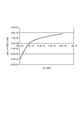
- the graph showing the gain spectrum of the active layer of SOA of Embodiment 1 of this invention The graph showing the relationship between the carrier density N in SOA of Embodiment 1 of this invention, and the sum total ⁇ g (N) of the positive gain obtained in the object wavelength range.
- 3 is a graph showing a relationship between an incident light wavelength ⁇ and L g , N g , and N a for achieving an optimum driving state in the SOA according to the first embodiment of the present invention.
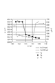
- 3 is a graph showing a relationship between an incident light wavelength ⁇ and a carrier density N in each electrode region for achieving an optimum driving state in the SOA according to the first embodiment of the present invention.
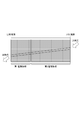
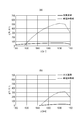
- the graph showing the relationship between the wavelength ⁇ and the incident light wavelength (a) 1030, (b) g (N, ⁇ ) ⁇ L in the optimum driving state in the SOA and the single electrode configuration SOA according to the first embodiment of the present invention. .
- FIG. 6 is a graph showing the relationship between the wavelength ⁇ and the incident light wavelength (a) 1030 and (b) g (N, ⁇ ) ⁇ L that is optimally driven at 1060 nm in the SOA and the single electrode configuration SOA according to the second embodiment of the present invention. .
- FIG. 6 is a graph showing the relationship between the wavelength ⁇ and the incident light wavelength (a) 1030 and (b) g (N, ⁇ ) ⁇ L that is optimally driven at 1060 nm in the SOA and the single electrode configuration SOA according to the second embodiment of the present invention. .
- the graph showing the sweep spectrum of the target emission light in SOA of Embodiment 4 of this invention.
- 10 is a graph showing a relationship between an incident light wavelength ⁇ and a carrier density N in each electrode region for achieving an optimum driving state in the SOA according to the fourth embodiment of the present invention.
- FIG. 6 is a graph showing the relationship between the wavelength ⁇ and the incident light wavelength (a) 1030 and (b) g (N, ⁇ ) ⁇ L that is optimally driven at 1060 nm in the SOA and the single electrode configuration SOA according to the second embodiment of the present invention. .
- optical amplifier according to the embodiment of the present invention will be described, the present invention is not limited to these.
- the optical amplifier according to the present embodiment has a stacked structure including two electrode layers and an active layer provided therebetween.
- the laminated body there is a structure having a lower electrode layer, a lower cladding layer, an active layer, an upper cladding layer, a contact layer, and an upper electrode layer in this order.
- What the stack is made of a semiconductor is called a semiconductor optical amplifier (hereinafter sometimes abbreviated as SOA).
- SOA semiconductor optical amplifier
- the end surface of the laminate on the side on which light is incident on the SOA may be referred to as the incident end surface
- the end surface on the side from which light is emitted may be referred to as the emission end surface
- This laminate has a waveguide through which light is guided in the in-plane direction of the active layer, and incident light on the end face side (incident end face side) in the in-plane direction of the laminate passes through the waveguide and is laminated. Amplified and emitted from the other end face side (injection end face side) in the in-plane direction of the body.
- the waveguide structure include a ridge waveguide in which an upper electrode layer, an upper contact layer, and an upper cladding layer form a ridge structure.
- At least one of the two electrode layers provided above and below the active layer has an electrode group composed of two or more electrodes provided separately in the waveguide direction of the waveguide.
- the optical amplifier according to the present embodiment uses two or more electrodes constituting an electrode group, and independently injects current into a plurality of different regions in the active layer, so that the optical amplifier according to the wavelength of incident light.
- the amplification factor can be changed.
- the optical amplifier according to this embodiment changes the amplification factor of incident light according to the wavelength of incident light, thereby selectively amplifying only the necessary wavelength to obtain sufficient light output intensity, Generation of ASE light including light of unnecessary wavelength can be suppressed as much as possible. For example, when it is desired to amplify light of wavelength ⁇ 1 out of incident light, the amount of current injected into the optical amplifier is adjusted, and light of wavelength ⁇ 1 is emitted from the optical amplifier with sufficient light output intensity. Like that. If the emitted light contains ASE light including unnecessary wavelengths, the region where light is amplified by injecting current into the optical amplifier is shortened to include light having a wavelength other than ⁇ 1. Reduce generation of ASE light.
- the optical amplifier in addition to the current injection amount (current density) into the optical amplifier, by changing the region where the light is amplified, it is possible to amplify a specific wavelength and suppress amplification of other wavelengths.
- the region where the light is amplified can be adjusted because the electrode layer constituting the laminate is provided by being separated into a plurality of electrodes, and current injection can be controlled independently. Control of the amount of current injected into each electrode is controlled by the control unit.
- the optical amplifier and the control unit may be collectively referred to as a light source system.
- the region in the waveguide, where the gain is positive at the wavelength of the incident light is defined as the gain region, and the total length of the gain regions along the waveguide is defined as the gain length.
- the gain region is defined as the gain region
- the total length of the gain regions along the waveguide is defined as the gain length.
- the current density of the current injected into the active layer is large, it is easy to amplify short wavelength light and it is difficult to amplify long wavelength light. Therefore, the shorter the wavelength of incident light, the more injected into the active layer. It is preferable to increase the current density.
- the waveform (spectral shape) of the wavelength change of the light emitted from the optical amplifier has either a substantially Gaussian shape or a substantially cosine tapered shape. This is because when such spectrally shaped light is used as OCT measurement light, it is easy to obtain an OCT image with less noise.
- the substantially Gaussian shape, the substantially rectangular shape, and the substantially cosine taper shape are not only Gaussian shape and cosine taper shape, but are slightly deviated from the Gaussian shape and cosine taper shape within a range in which large noise does not appear in the OCT image. It is a concept that includes a shape.
- the electrode group is composed of at least three electrodes and no current is injected into at least one electrode of the electrode group
- the electrode to which no current is injected is provided at a position closest to the incident end face of the laminate. It is preferably not an electrode.
- the electrode into which no current is injected is preferably an electrode provided at a position closest to the end face from which light is emitted.
- the current density of the electrode group is substantially the same.
- the gain in one optical width device can be changed with time mainly by the current density in the electrode region.
- a region where the gain at the center wavelength of incident light is positive is defined as a gain region, and a region where the gain is zero or less is defined as a non-gain region.
- optical amplifier according to the embodiment of the present invention will be described in detail with a specific configuration.
- the configurations, dimensions, materials, and control methods given in the following embodiments are merely examples, and the present invention is not limited to these.
- MEMS-VCSEL will be described as an example of a wavelength swept light source that performs wavelength sweeping by the MEMS mechanism.
- the MEMS-VCSEL of this example is configured to displace one mirror (sometimes referred to as a MEMS mirror) that constitutes a VCSEL resonator by electrostatic attraction.
- Embodiment 1 of the present invention will be described below.
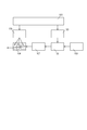
- the same signal is sent from a waveform generator 101 to a voltage amplifier 103 that controls the MEMS driving of the wavelength swept light source 102 and a current controller (control unit) 105 that controls the driving of the SOA 104.
- a current controller control unit
- the MEMS drive of the wavelength swept light source 102 and the drive of the SOA 104 can be synchronized in time. Therefore, by grasping the relationship between the voltage value for controlling the displacement of the MEMS mirror of the wavelength swept light source 102 and the oscillation wavelength in advance, the drive current value of the SOA 104 can be controlled according to the oscillation wavelength. become.
- an isolator 107 is provided between the wavelength swept light source 102 and the SOA 104 in order to suppress return light to the wavelength swept light source 102.
- FIG. 2 is a perspective view (b) of the SOA in this embodiment, and is a top view of the SOA.
- 3A is a cross-sectional view of a region (aa ′ cross section) where an SOA electrode is provided in the present embodiment
- FIG. 3B is a non-electrode region (bb ′ cross section) where no electrode is provided.
- FIG. 3C is a sectional view of the optical waveguide (c-c ′ section) of the SOA in the present embodiment.
- all electrodes are connected to a drive system (driver), and the amount of current (current density) injected into the active layer can be controlled independently for each electrode region. It has a mechanism.
- n-Al 0.9 GaAs as an n-type cladding layer 211 is sequentially epitaxially grown on the GaAs substrate 210 by using, for example, a MOCVD (Metal Organic Chemical Vapor Deposition) method.
- MOCVD Metal Organic Chemical Vapor Deposition
- GaIn 0.3 As having a single quantum well structure as the active layer 205, p-Al 0.9 GaAs as the p-type cladding layer 212, and highly doped p-GaAs as the contact layer 213 are epitaxially grown sequentially.
- a ridge 206 is formed on the wafer on which each layer is laminated by a general photolithography method and wet / dry etching to form an optical waveguide.
- the ridge 206 By forming the ridge 206, light can be confined and guided in the waveguide portion in the active layer.
- a stripe mask for forming an optical waveguide is formed of a photoresist using a photolithography method. Thereafter, SiO 2 is selectively removed by wet etching, and the semiconductor other than the mask is selectively removed by dry etching. At this time, the part to be removed is halfway between the contact layer 213 and the p-type cladding layer 212.
- the width of the optical waveguide is 3 ⁇ m in order to achieve a single mode.
- the optical waveguide In order to suppress reflection at the incident end face 201 and the exit end face 202, the optical waveguide is inclined about 7 degrees with respect to the normal direction of each end face in the vicinity of the end face.
- the p-electrode 203 is formed using a vacuum deposition method and photolithography.
- the p electrode 203 is, for example, Ti / Au, and a plurality of p electrodes 203 are arranged on the optical waveguide in a state where they are insulated in series with respect to the waveguide direction. Further, the contact layer 213 in the non-electrode region is removed by wet etching using citric acid perwater to form an electrically insulated region.
- the substrate 210 is thinned to a thickness of about 100 ⁇ m by polishing. By doing so, cleavage on the facet surface is facilitated. Then, the n electrode 204 is formed by a vacuum evaporation method.
- the n electrode 204 is, for example, AuGe / Ni / Au.
- annealing is performed in a high-temperature nitrogen atmosphere to alloy both electrodes and the semiconductor.
- a facet surface is formed on the incident end face 201 and the exit end face 202 by cleavage, thereby completing the SOA element.
- the substrate 210 may be a p-type GaAs substrate, in which case the conductivity type of each semiconductor layer is changed accordingly.
- the active layer 205 has an example of a single quantum well (SQW) structure
- a multiple quantum well (MQW) structure having a plurality of quantum wells may be used.
- the MQW structure may be an asymmetric multiple quantum well (A-MQW) structure (asymmetric quantum well structure) in which the composition and well width are the same, or at least one of the plurality of quantum wells has a different composition or well width. Good.
- the material constituting the quantum well is not limited to the above-described materials, and a light emitting material such as GaAs, GaInP, AlGaInN, AlGaInAsP, AlGaAsSb may be used.
- the active layer 205 has a single thickness and a single composition with respect to the waveguide direction, but is not limited to this as long as the effects of the present invention can be obtained.
- the optical waveguide has a linear shape, a constant width, and a shape capable of obtaining a constant refractive index, but is not limited to this as long as the effect of the present invention can be obtained.
- the optical waveguide shape may be bent or branched, and the width or refractive index of the optical waveguide may be changed in the waveguide direction.
- the optical waveguide width is 3 ⁇ m so that the light emitted from the SOA becomes a single (single) mode
- it may be made to be a multi (multi) mode.
- a stripe type active layer or a current blocking layer may be introduced to confine the current or light.
- the SOA in the present embodiment shows an example in which the optical waveguide is inclined by about 7 degrees with respect to the normal direction of each end face in the vicinity of the end face in order to suppress reflection at each end face of the entrance end face and the exit end face.
- the angle is not limited to 7 °.
- the number of electrodes included in the electrode group is three is shown, but the number of electrodes satisfying the requirement for obtaining the effect of the present invention (two or more) is not limited thereto.
- a non-gain region may be formed in the vicinity of the end face in order to suppress concentration of light and current on the end face of the incident end face 201 and / or the end face 202 of the emission.
- An antireflection (AR) film may be formed on the end face in order to suppress reflection at the end face of the incident end face 201 or the exit end face 202 or both.
- a configuration in which a plurality of n electrodes 204 or both electrodes are arranged may be used.
- the SOA driving state is defined by the carrier density, but in practice, the current density in each electrode region is adjusted so that the carrier density in the gain region and the non-gain region becomes a desired value.
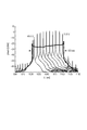
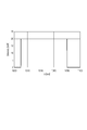
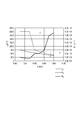
- the sweep spectrum of the MEMS-VCSEL having a center wavelength near 1060 nm as the incident light (FIG. 4) and the sweep spectrum shape (shown by a solid line in FIG. 5) represented by the following equation as the target emission light Assumed.
- FIG. 4 quotes Electron Let 2012 Oct 11 48 (21) 1331-1333.
- ⁇ is the wavelength and P is the light intensity.
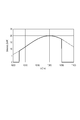
- This sweep spectrum has a Gaussian shape (indicated by a dotted line in FIG. 5) having a center wavelength of 1060 nm, a light intensity at the center wavelength of 20 mW, and a full width at half maximum of 90 nm in the sweep wavelength range (1010 to 1080 nm) of incident light. In other wavelength ranges, the light intensity is 0 mW.
- the plurality of gain regions have the same carrier density. Further, the carrier density is such that the gain at the incident light wavelength is zero in the non-gain region.
- ⁇ wavelength (1010 to 1080 nm)
- P in ( ⁇ ) incident light intensity at wavelength ⁇
- P out ( ⁇ ) emitted light intensity at wavelength ⁇ .
- G (N, ⁇ ): SOA gain at wavelength ⁇ at carrier density N, L g : total length of SOA gain region, and ⁇ : confinement factor in SOA optical waveguide. In the following, calculation results with ⁇ 0.03 are shown.
- FIG. 6 shows a gain spectrum in the active layer of the SOA of the present embodiment.
- ⁇ g (N) is used as an index representing the total amount of ASE light per unit length of the gain region generated from the SOA itself at the carrier density N in the target wavelength range.
- the optimum driving state refers to a driving state in which incident light of a certain wavelength (in this case, wavelength 1060 nm) is amplified and ASE light is reduced as much as possible so as to form a desired sweep spectrum.
- the driving state here refers to a combination of the length of each electrode region and the carrier density in those electrode regions. In other words, when the total length (gain length) and carrier density of the gain region are L g and N g , respectively, and the total length of the non-gain region (non-gain length) and the carrier density are L a and N a , respectively, optimum driving In order to determine the state, it is necessary to determine these four values.
- N g and N a for obtaining the optimum driving state are obtained.
- g (N, ⁇ ) / ⁇ g (N) represents the magnitude of the gain at the wavelength ⁇ with respect to the total amount of ASE light in the target wavelength range, and the larger the value, the smaller the wavelength ⁇ while suppressing the amount of ASE light. This means that incident light can be amplified efficiently.
- g (N, ⁇ ) / ⁇ g (N) represents the magnitude of the gain at the wavelength ⁇ with respect to the total amount of ASE light in the target wavelength range, and the larger the value, the smaller the wavelength ⁇ while suppressing the amount of ASE light. This
- N g for achieving the state is determined to be 2.2E + 18 / cm 3 .
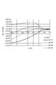
- FIG. 10 shows the results of obtaining L g , N g , and N a for achieving the optimum driving state with respect to the target wavelength range of 1010 to 1080 nm.
- L g for the optimum driving condition is long, N g and N a tends to be lowered.
- the number of electrodes is three, it is possible to obtain an optimum gain length for at least three wavelengths of incident light.
- L g for achieving an optimum driving state at incident light wavelengths of 1010, 1040, and 1080 nm are 417, 920, and 3630 ⁇ m, respectively, from FIG. Therefore, if the length of the n-th electrode is L n , L 1 , L 2 , and L 3 in FIG.
- the gain length for achieving the optimum driving state cannot be obtained at wavelengths other than the selected three wavelengths, but it is possible to approach the optimum driving state by considering a combination that is closest to the combination of the electrode lengths.
- N n is the carrier density in the n-th electrode region
- N 1 , N 2 , N 3 , and L g for obtaining an optimum driving state with respect to the incident light wavelength ⁇ are summarized as shown in FIG.
- the N g black circle shows the plot point N a by white circles.
- the target emission light is calculated assuming a Gaussian-shaped sweep spectrum having a center wavelength of 1060 nm, a light intensity of 20 mW at the center wavelength, and a full width at half maximum of 90 nm.
- the center wavelength, the light intensity at the center wavelength, the full width at half maximum, and the sweep spectrum shape are not limited to this (see Embodiment 4 for the rectangular shape).
- the plurality of gain regions have the same carrier density, but there is a range where the effect can be obtained even if the carrier densities are not the same.
- the non-gain region shows an example in which the carrier density is such that the gain at the incident light wavelength is zero, but it is effective if the gain with respect to the incident light wavelength is equal to or less than zero, and may be driven with zero or reverse bias.
- the non-gain region and the drive system may not be connected, or the electrode may not be formed in the non-gain region.
- the wavelength in the optimum driving state is 1010, 1040, 1080 nm
- the wavelength is not limited to this wavelength as long as it is within the target wavelength range.
- the setting is made to vary within the target wavelength range.
- the electrode shows an example of a three-electrode configuration, but the effect of the present invention can be obtained if there are two or more (see Embodiment 2 for the two-electrode configuration).
- a configuration may be adopted in which a large number of electrodes having a short length (for example, 10 ⁇ m) are arranged. By doing so, it becomes possible to approach the gain length for achieving a more optimal driving state (refer to Embodiment 3 for the electrode configuration capable of finely setting the gain region). However, with this configuration, absorption in the non-electrode region increases, and it may be difficult to control the electrode configuration and driving state.
- the same effect can be obtained even when there are more electrodes if the driving state is substantially the same.
- L a will may be designed long. However, if the length is increased, the amount of unnecessary ASE light increases, so it is desirable to shorten it as much as possible.
- SOA gain spectrum control method Another configuration example of the SOA and the wavelength swept light source according to the present embodiment will be described.
- the wavelength swept light source 102 is driven, and the emitted light is demultiplexed by a beam splitter (not shown). A part of the demultiplexed light is detected as a monitor light by a line sensor (not shown), and a signal corresponding to the center wavelength of the monitor light is transmitted to the control unit 105. Then, current is injected into each electrode of the SOA 104 based on the signal. With such a configuration, the SOA 104 can be controlled to a gain spectrum corresponding to the wavelength of light actually emitted from the wavelength swept light source.
- the same signal is sent from the waveform generator 101 to a voltage amplifier (not shown) for controlling the MEMS drive of the wavelength swept light source 102 and the current controller 105 of the SOA, and the SOA is a gain spectrum corresponding to the light emitted from the wavelength swept light source. You may control to become.
- the table also shows the correspondence between the time variation of the wavelength of the light emitted from the wavelength swept light source 102 and the current value that needs to be injected into the SOA in order to perform optical amplification suitable for each wavelength of the emitted light. It is also possible to have a memory (not shown) stored as
- the optical amplification method according to the present embodiment uses the semiconductor optical amplifier as described in the first embodiment. Specifically, at least one of the electrode layers constituting the semiconductor optical amplifier has an electrode group including two or more electrodes separated in the waveguide direction of the optical waveguide of the semiconductor optical amplifier. .
- the optical amplification method in this embodiment has at least the following three steps.
- the amplification step (3) by using two or more electrodes of the semiconductor optical amplifier, current is independently injected into a plurality of different regions in the active layer of the semiconductor optical amplifier, and according to the wavelength of incident light, Changing the light amplification factor.
- the amplification step preferably includes a step of changing the gain length according to the wavelength of the incident light.
- the amplification step preferably includes a step of shortening the gain length as the wavelength of incident light is shorter.
- the amplification step has a step of injecting current into the active layer so that the carrier density of the active layer increases as the wavelength of incident light is shorter.
- the amplification step has a step of shortening the gain region as the wavelength of incident light is shorter.
- Embodiment 2 of the present invention is shown below.
- FIG. 13 shows a top view of the element configuration of the SOA in the present embodiment.
- the present embodiment is the same as the first embodiment except for the electrode configuration and the driving state. Therefore, only differences from the first embodiment will be described.
- the upper electrode layer has an electrode group including two electrodes. Therefore, the derivation of the optimum driving state and the actual driving can be executed more easily.
- the electrode length is designed so that the optimum driving state can be achieved with respect to, for example, 1020 and 1070 nm.
- the optimum driving state is derived by the method shown in the first embodiment, and N 1 , N 2 , and L g for obtaining the optimum driving state with respect to the incident light wavelength ⁇ are summarized as shown in FIG.
- the N g black circle shows the plot point N a by white circles.
- Embodiment 3 of the present invention is shown below.
- FIG. 16 shows the element configuration of the SOA in the present embodiment.
- the present embodiment is the same as the first embodiment except for the electrode configuration and the driving state. Therefore, only differences from the first embodiment will be described.
- This embodiment is characterized by an electrode configuration in which the length of the electrode is regularly changed. By doing so, the gain length and the non-gain length due to the combination can be adjusted with a higher degree of freedom than in the first embodiment.
- the length of each electrode is set so that a gain length for obtaining an optimum driving state can be obtained with respect to a certain incident light wavelength.
- the optimum driving state is obtained at other wavelengths. Therefore, it cannot be a gain length.
- L 1 to L 8 are set to 20, 40, 80, 160, 320, 640, 1280, 1090 ⁇ m (in no particular order).
- the gain length for achieving the optimum driving state can be obtained at the incident light wavelength of 1080 nm where the gain length for achieving the optimum driving state is the largest value.
- the difference between the gain length for achieving the optimum driving state at each incident light wavelength and the actual gain length can be suppressed to less than 10 ⁇ m.
- the optimum driving state is derived by the method shown in the first embodiment, and the lengths and carrier densities of the respective electrode regions for obtaining the optimum driving state with respect to the incident light wavelength are summarized as shown in FIG.
- the same effect can be obtained even if the length of each electrode described above and the driving state corresponding to the electrode are interchanged.
- the colored carrier density represents the carrier density in the non-gain region.
- the minimum unit of the electrode is 20 ⁇ m
- the same effect as in the present embodiment can be obtained with values of 10 ⁇ m, 50 ⁇ m, and 100 ⁇ m.
- the thickness is less than 10 ⁇ m, the absorption in the non-electrode region increases, and it may be difficult to control the electrode configuration and the driving state.
- Embodiment 4 of the present invention will be described below.
- the present embodiment is the same as the first embodiment except for the target emission light. Therefore, only differences from the first embodiment will be described. Therefore, the sample configuration is as shown in FIG. 3, but the length and driving state of the electrodes are different from those of the first embodiment.
- the target emission light in the present embodiment assumes a rectangular sweep spectrum (FIG. 18) having a light intensity of 20 mW at a wavelength of 1010 to 1080 nm.
- the method for deriving the optimum driving state is as described in the first embodiment.
- the electrode length is designed so that the optimum driving state can be achieved with respect to 1010, 1040, 1080 nm, for example.
- FIG. 19 shows the results of determining L g , N g , and N a for achieving the optimum driving state with respect to the target wavelength range of 1010 to 1080 nm. Furthermore, FIG. 20 shows the N 1 , N 2 , N 3 , and L g for deriving the optimum driving state and setting the optimum driving state for the incident light wavelength ⁇ .
- the N g black circle shows the plot point N a by white circles.
- Embodiment 5 of the present invention will be described below.
- the OCT apparatus includes a light source unit 301 (MEMS-VCSEL) in which the emitted optical frequency is swept, an optical amplifier (SOA) 302 that performs optical output increase and sweep spectrum shape control, and an isolator 303 therebetween. Then, an interference unit 304 that generates interference light, a signal output unit 305 that receives the interference light and outputs an interference signal, and an acquisition unit 306 that acquires information on an object (subject) based on the interference signal Have. Further, the OCT apparatus has a measurement arm (irradiation optical system) 307 and a reference arm (reference optical system) 308.
- the interference unit 304 includes two couplers 310 and 311.
- the coupler 310 branches the light emitted from the light source into irradiation light for irradiating the subject 312 and reference light.
- the irradiation light is irradiated to the subject 312 via the measurement arm 307. More specifically, the irradiation light incident on the measurement arm 307 is adjusted in polarization state by the polarization controller 313 and then emitted from the collimator 314 as spatial light. Thereafter, the irradiated light is irradiated to the subject 312 via the X-axis scanner 315, the Y-axis scanner 316, and the focus lens 317.
- the X-axis scanner 315 and the Y-axis scanner 316 are scanning units having a function of scanning the subject 312 with irradiation light.
- the irradiation position of the irradiation light on the subject 312 is changed by the scanning unit.
- the back scattered light (reflected light) from the subject 312 is emitted from the measurement arm 307 via the focus lens 317, the Y-axis scanner 316, the X-axis scanner 315, the collimator 314, and the polarization controller 313 again.
- the light enters the coupler 311 via the coupler 310.
- the interference unit 304, the measurement arm 307, and the reference arm 308 can be collectively referred to as an interference optical system.
- the interference optical system is a Mach-Zehnder type, but may be a Michelson type.
- the reference light enters the coupler 311 via the reference arm 308. More specifically, the reference light incident on the reference arm 308 is emitted from the collimator 319 as spatial light after its polarization state is adjusted by the polarization controller 318. Thereafter, the reference light passes through the dispersion compensation glass 320, the optical path length adjustment optical system 321, and the dispersion adjustment prism pair 322, enters the optical fiber through the collimator lens 323, exits from the reference arm 308, and enters the coupler 311.
- the signal output unit 305 includes a differential detector 324 and an A / D converter 325.
- the differential detector 324 detects the interference light that is demultiplexed immediately after the interference light is generated by the coupler 311.
- the interference signal converted into an electrical signal by the differential detector 324 is converted into a digital signal by the A / D converter 325.
- the digital signal is sent to the information acquisition unit 306, and frequency analysis such as Fourier transform is performed on the digital signal, whereby information on the subject 312 is obtained.
- Information about the obtained subject 312 is displayed as a tomographic image by the display unit 326.
- the sampling timing of the interference light is performed at equal optical frequency (equal wave number) intervals based on a k clock signal transmitted from a k clock generation unit 327 provided outside the light source.
- a coupler 309 is provided to branch a part of the light emitted from the light source to the k clock generation unit 327.
- k clock generation unit 327 and the coupler 309 may be incorporated in the light source 301 or the SOA 302.
- A-scan Acquiring information about a tomography in the depth direction of the subject 312 is called A-scan.
- the information about the tomography of the subject 312 in the direction orthogonal to the A-scan is orthogonal to the scanning direction of B-scan, and further, the A-scan and B-scan. Scanning in this direction is called C-scan.
- C-scan This is because, when acquiring a three-dimensional tomographic image, when performing two-dimensional raster scanning in the fundus, the high-speed scanning direction is B-scan, and the low-speed scanning direction in which B-scan is arranged in the orthogonal direction is C- Call it scan.
- a two-dimensional tomographic image can be obtained by performing A-scan and B-scan, and a three-dimensional tomographic image can be obtained by performing A-scan, B-scan and C-scan.
- B-scan and C-scan are performed by the X-axis scanner 315 and the Y-axis scanner 316 described above.
- the X-axis scanner 315 and the Y-axis scanner 316 are composed of deflection mirrors that are arranged so that their rotation axes are orthogonal to each other.
- the X-axis scanner 315 performs scanning in the X-axis direction
- the Y-axis scanner 316 performs scanning in the Y-axis direction.
- the X-axis direction and the Y-axis direction are directions perpendicular to the surface normal of the subject and perpendicular to each other.
- the line scanning direction such as B-scan and C-scan may not coincide with the X-axis direction or the Y-axis direction. Therefore, the B-scan and C-scan line scanning directions can be appropriately determined according to a two-dimensional tomographic image or a three-dimensional tomographic image to be imaged.
- a characteristic of this embodiment is the SOA.
- the SOA of the present invention described in the above embodiment is used, the ASE light can be reduced while controlling the sweep spectrum shape of the MEMS-VCSEL, so that high-resolution tomographic image information can be obtained. Will be advantageous to get.
- This OCT apparatus is mainly useful for tomographic imaging in ophthalmology.
Landscapes
- Physics & Mathematics (AREA)
- General Physics & Mathematics (AREA)
- Health & Medical Sciences (AREA)
- Life Sciences & Earth Sciences (AREA)
- Condensed Matter Physics & Semiconductors (AREA)
- Electromagnetism (AREA)
- Optics & Photonics (AREA)
- General Health & Medical Sciences (AREA)
- Molecular Biology (AREA)
- Veterinary Medicine (AREA)
- Engineering & Computer Science (AREA)
- Biomedical Technology (AREA)
- Heart & Thoracic Surgery (AREA)
- Medical Informatics (AREA)
- Biophysics (AREA)
- Surgery (AREA)
- Animal Behavior & Ethology (AREA)
- Radiology & Medical Imaging (AREA)
- Public Health (AREA)
- Ophthalmology & Optometry (AREA)
- Nuclear Medicine, Radiotherapy & Molecular Imaging (AREA)
- Analytical Chemistry (AREA)
- Biochemistry (AREA)
- Immunology (AREA)
- Pathology (AREA)
- Chemical & Material Sciences (AREA)
- Geometry (AREA)
- Semiconductor Lasers (AREA)
- Investigating Or Analysing Materials By Optical Means (AREA)
- Eye Examination Apparatus (AREA)
Abstract
2つの電極層と、それらの間に設けられた活性層とを含む積層体を有し、前記積層体は、前記活性層の面内方向に光が導波される導波路を有し、前記積層体への入射光が、前記導波路を経て、前記積層体の面内方向の端面側から増幅されて射出される光増幅器であって、前記2つの電極層の少なくともいずれか一方は、前記導波路の導波方向に分離されて設けられた2つ以上の電極を含む電極群を有し、前記光増幅器は、前記2つ以上の電極を用いて、前記活性層における複数の異なる領域に独立に電流を注入することで、前記入射光の波長に応じて、前記入射光の増幅率を変化させることが可能に構成されている光増幅器。必要な波長において十分な光出力強度を得つつ、不必要な波長の光を含むASE光を低減可能な光増幅器を提供すること。
Description
本発明は、波長可変光源から出る光を増幅する光増幅器、それを備える光干渉断層計、及び光増幅器を用いた光増幅方法に関する。
眼底などの撮像装置として、光干渉断層計(Optical Coherence Tomography、以下OCTという)が知られている。特に、波長可変光源を用いたOCT(Swept Source OCT、以下SS-OCTと略すことがある)が注目されている。SS-OCTは、波長可変光源から出た光を物体へ照射する照射光と、参照光とに分け、参照光と、物体の異なる深さから戻ってくる反射光とを干渉させる。そして、干渉光の強度の時間波形(干渉信号)に含まれる周波数成分を分析することで、物体の断層に関する情報、具体的には断層像を得ることができる。OCTは、例えば眼科、循環器科、皮膚科、半導体チップの検査等の工業用途で用いられている。
波長可変光源の1つとして、垂直共振器型の面発光レーザ(Vertical Cavity Surface Emitting Laser、VCSEL)を構成する2枚の反射鏡のうちの片方を変位させて発振波長を変える波長可変光源が知られている。ミラーを動かすための機構としては、MEMSを用いたものが知られている。以下、このような波長可変光源をMEMS-VCSELと呼ぶことがある。MEMS-VCSELは、高速に波長可変可能であり、かつコヒーレンス長を長くできることが知られているため、SS-OCTに用いる波長可変光源として好適である。
ここで、十分なS/N比のOCT信号を得るために、OCTに用いられる光源は必要な強度の光出力が得られることが好ましい。しかし、波長可変光源として、VCSEL単体を用いた場合、必要な強度の光出力を得ることは難しい。そこで、非特許文献1では、MEMS-VCSELから出た光を、光増幅器(BOA、Booster OpticalAmplifier)を用いて誘導増幅させることで、必要な光出力強度を得ている。
Journal of Lightwave Technology 33(16)p.3461-3468
ここで、本発明者は、非特許文献1に開示のBOAを用いた光出力強度の増幅には課題があることを見出した。すなわち、BOAを用いて増幅するときに、BOA自体からASE(Amplified Spontaneous Emission)光が発生してしまう。ASE光はBOA自体から発生する自然放出光であり、ASE光には、増幅させたい波長以外の波長の光が含まれる。そのため、ASE光を含む光が照射されて得られたOCT信号にはノイズが含まれてしまう。
非特許文献1では、時間的に波長が変化する入射光に対するBOAの増幅率を、時間的に変化させることが記載されている。BOAに注入する電流量を大きくすることで増幅率を上げ、ある波長において必要な強度の光を得ることができる。しかし、電流量の調整だけでは、ある波長における必要な光出力強度が得られても、不必要な波長の光を含むASE光の強度も大きくなってしまう場合がある。非特許文献1には、このような、BOAのASE光を低減するための制御について何ら開示がない。
そこで本発明は、上記課題に鑑み、必要な波長において十分な光出力強度を得つつ、不必要な波長の光を含むASE光を低減可能な光増幅器を提供することを目的とする。
本発明に係る光増幅器は、2つの電極層と、それらの間に設けられた活性層とを含む積層体を有し、前記積層体は、前記活性層の面内方向に光が導波される導波路を有し、前記積層体への入射光が、前記導波路を経て、前記積層体の面内方向の端面側から増幅されて射出される光増幅器であって、前記2つの電極層の少なくともいずれか一方は、前記導波路の導波方向に分離されて設けられた2つ以上の電極を含む電極群を有し、前記光増幅器は、前記2つ以上の電極を用いて、前記活性層における複数の異なる領域に独立に電流を注入することで、前記入射光の波長に応じて、光の増幅率を変化させることが可能に構成されている。
本発明に係る光増幅器によれば、光増幅器を構成する積層体の電極層の少なくともいずれか一方を複数に分割することによって、光増幅器の増幅率に加えて、増幅される領域を変えることができる。そのため、必要な波長において十分な光出力強度を得つつ、不必要な波長の光を含むASE光を低減できる。
本発明の実施形態に係る光増幅器について説明するが、本発明はこれらに限られない。
(光増幅器)
本実施形態に係る光増幅器は、2つの電極層と、それらの間に設けられた活性層とを含む積層体の構造を有する。積層体の一例として、下部電極層、下部クラッド層、活性層、上部クラッド層、コンタクト層、上部電極層の順に有する構造が挙げられる。積層体が半導体で構成させるものは、半導体光増幅器(Semiconductor Optical Amplifier、以下SOAと略すことがある)と呼ばれる。以下では、SOAに入射する光を入射光、SOAから出る光を射出光と呼ぶことがある。
本実施形態に係る光増幅器は、2つの電極層と、それらの間に設けられた活性層とを含む積層体の構造を有する。積層体の一例として、下部電極層、下部クラッド層、活性層、上部クラッド層、コンタクト層、上部電極層の順に有する構造が挙げられる。積層体が半導体で構成させるものは、半導体光増幅器(Semiconductor Optical Amplifier、以下SOAと略すことがある)と呼ばれる。以下では、SOAに入射する光を入射光、SOAから出る光を射出光と呼ぶことがある。
また、SOAに光が入射される側の積層体の端面を入射端面、光が射出される側の端面を射出端面と呼ぶことがある。
この積層体は、活性層の面内方向に光が導波される導波路を有し、積層体の面内方向の端面側(入射端面側)への入射光が、導波路を経て、積層体の面内方向のもう一方の端面側(射出端面側)から増幅されて射出される。導波路構造は例えば、上部電極層、上部コンタクト層、上部クラッド層がリッジ構造を形成してなるリッジ導波路が挙げられる。
また、活性層の上下に設けられた2つの電極層の少なくともいずれか一方は、導波路の導波方向に分離されて設けられた2つ以上の電極からなる電極群を有している。
本実施形態に係る光増幅器は、電極群を構成する2つ以上の電極を用いて、活性層における複数の異なる領域に独立に電流を注入することで、入射光の波長に応じて、光の増幅率を変化させることが可能に構成されている。
なお、活性層における複数の異なる領域に独立に電流を注入するための制御部を有していても良い。
(入射光の波長に応じた光増幅率の制御)
本実施形態に係る光増幅器は、入射光の波長に応じて、入射光の増幅率を変化させることにより、必要な波長のみを選択的に増幅させて十分な光出力強度を得つつ、それ以外の不必要な波長の光を含むASE光の発生を極力抑えることが出来る。例えば、入射光のうち波長λ1の光を増幅させたい場合は、光増幅器への電流注入量を調整して、λ1の波長の光が、光増幅器から十分な光出力強度をもって射出されるようにする。射出される光に、不必要な波長を含むASE光が含まれてしまう場合は、光増幅器に電流が注入されて光が増幅される領域を短くして、λ1以外の波長の光を含むASE光の発生を低減する。すなわち、光増幅器への電流注入量(電流密度)に加えて、光が増幅される領域を変えることで、特定の波長を増幅させ、それ以外の波長の増幅を抑制させることができる。光が増幅される領域を調整できるのは、上記積層体を構成する電極層が複数の電極に分離されて設けられ、電流注入を独立に制御できるからである。各電極への電流注入量の制御は、制御部によって制御される。光増幅器と制御部とを合わせて光源システムと呼んでも良い。
本実施形態に係る光増幅器は、入射光の波長に応じて、入射光の増幅率を変化させることにより、必要な波長のみを選択的に増幅させて十分な光出力強度を得つつ、それ以外の不必要な波長の光を含むASE光の発生を極力抑えることが出来る。例えば、入射光のうち波長λ1の光を増幅させたい場合は、光増幅器への電流注入量を調整して、λ1の波長の光が、光増幅器から十分な光出力強度をもって射出されるようにする。射出される光に、不必要な波長を含むASE光が含まれてしまう場合は、光増幅器に電流が注入されて光が増幅される領域を短くして、λ1以外の波長の光を含むASE光の発生を低減する。すなわち、光増幅器への電流注入量(電流密度)に加えて、光が増幅される領域を変えることで、特定の波長を増幅させ、それ以外の波長の増幅を抑制させることができる。光が増幅される領域を調整できるのは、上記積層体を構成する電極層が複数の電極に分離されて設けられ、電流注入を独立に制御できるからである。各電極への電流注入量の制御は、制御部によって制御される。光増幅器と制御部とを合わせて光源システムと呼んでも良い。
なお、光が増幅される領域を利得長と言い換えることができる。
ここで、入射光の波長において利得が正である、導波路内の領域を利得領域、導波路に沿った利得領域の合計長さが利得長と定義される。具体的には、入射光の波長が、長波長であるほど利得長を長くすることで、長波長の光を選択的に増幅可能であり、短波長であるほど利得長を短くすることで、短波長の光を選択的に増幅可能である。利得長を短くする方法としては、活性層に注入するために用いられる電極を減らす方法がある。したがって、短波長であるほど光増幅器の活性層に電流注入するための電極の数を少なくすることで、短波長の光を選択的に増幅可能である。逆もまた同様である。
また、活性層に注入される電流の電流密度が大きいと、短波長の光を増幅しやすく、長波長の光を増幅しにくくなるため、入射光の波長が短いほど、活性層に注入される電流密度を大きくすることが好ましい。
なお、光増幅器から射出される光の波長の時間変化の波形(スペクトル形状)は、略ガウシアン形状、略コサインテーパ形状のいずれかであることが好ましい。なぜなら、そのようなスペクトル形状の光がOCTの測定光として用いられると、ノイズの少ないOCT像が得られやすいからである。
ここで、略ガウシアン形状、略矩形形状、略コサインテーパ形状とは、ガウシアン形状、コサインテーパ形状だけでなく、OCT像に大きなノイズがのらない範囲で、ガウシアン形状、コサインテーパ形状から少しずれた形状を含む概念である。
また、電極群が少なくとも3つの電極から構成され、電極群のうち少なくとも1つの電極に電流が注入されない場合に、電流が注入されないその電極は、積層体の入射端面に最も近い位置に設けられた電極ではないことが好ましい。
また、電流が注入されない電極は光が射出される端面に最も近い位置に設けられた電極であることが好ましい。
また、電極群の電流密度が略同一になるように構成されていることが好ましい。
1つの光幅器における利得は、主に電極領域における電流密度により時間的に変化させることができる。光導波路上の領域のうち、入射光の中心波長における利得が正である領域を利得領域、ゼロ以下である領域を非利得領域とする。
以下、本発明の実施形態に係る光増幅器について、具体構成を挙げて詳細を説明する。以下の実施形態で挙げる構成、寸法、材料、制御方法は1つの例であり、本発明はこれに限定されるものではない。
なお、以下では光増幅器としてSOA、光源として、射出する光の波長をMEMS機構で掃引する波長掃引光源、を用いた構成を例に説明する。
また以下では、MEMS機構で波長掃引する波長掃引光源としては、前述のMEMS-VCSELを例に説明する。本例のMEMS-VCSELは、VCSELの共振器を構成する一方のミラー(MEMSミラーと呼ぶことがある)を静電引力で変位させる構成である。
(実施形態1)
以下に本発明の実施形態1を示す。
以下に本発明の実施形態1を示す。
本実施形態におけるSOAと、波長掃引光源について、図1を用いて説明する。
まず、波形発生装置(function generator)101から、波長掃引光源102のMEMS駆動を制御する電圧増幅器103と、SOA104の駆動を制御する電流制御器(制御部)105に同じ信号を送る。こうすることで、波長掃引光源102のMEMS駆動とSOA104の駆動を時間的に同期させることができる。したがって、あらかじめ波長掃引光源102のMEMSミラーの変位を制御するための電圧値と発振波長との関係を把握しておくことで、発振波長に応じてSOA104の駆動電流値を制御することができるようになる。
また、波長掃引光源102とSOA104との間には、波長掃引光源102への戻り光抑制のため、アイソレータ107が設けられる。
次に、本実施形態におけるSOAの構成を図2、3に示す。
図2は本実施形態におけるSOAの斜視図(b)はSOAの上面図である。図3(a)は本実施形態におけるSOAの電極が設けられている領域(a-a‘断面)の断面図、(b)は電極が設けられていない非電極領域(b-b’断面)の断面図である。図3(c)は本実施形態におけるSOAの光導波路(c-c‘断面)の断面図を示している。
なお、SOAは図1に示すように、全ての電極は駆動系(ドライバ)と接続されており、各電極領域に対してそれぞれ独立に、活性層に注入する電流量(電流密度)を制御できる機構を備えている。
次に、本実施形態に係るSOAの製造手順を説明する。
まず、GaAs基板210上に、n型クラッド層211としてn-Al0.9GaAs、を、例えばMOCVD(Metal Organic Chemical VaporDeposition)法を用いて順次エピタキシャル成長させる。同様にMOCVDで、活性層205として単一量子井戸構造のGaIn0.3As、p型クラッド層212としてp-Al0.9GaAs、コンタクト層213として高ドープのp-GaAsを、順次エピタキシャル成長させる。各層が積層されたウエハを一般的なフォトリソグラフィ法およびウェット/ドライエッチングにより、リッジ206を形成して光導波路を形成する。リッジ206を形成することにより、活性層内の導波路部分に光を閉じ込め、導波させることができる。たとえば、スパッタ法を用いてSiO2を形成した後、フォトリソグラフィ法を用いてフォトレジストで光導波路形成のためのストライプ状マスクを形成する。その後、ウェットエッチングによりSiO2、ドライエッチングによりマスク以外の部分の半導体を選択的に除去する。このとき、除去する部分はコンタクト層213とp型クラッド層212の途中までとする。光導波路幅は単一モードとするために3umの幅とする。入射端面201および射出端面202における反射を抑えるために、光導波路は端面付近で各端面の法線方向に対して約7度傾斜させている。
次に、真空蒸着法およびフォトリソグラフィを用いてp電極203を形成する。p電極203は、たとえばTi/Auであり、光導波路上に導波方向に対して直列にそれぞれが絶縁された状態で複数配置する。さらに、非電極領域のコンタクト層213をクエン酸過水を用いたウェットエッチングによる除去を行い、電気的に絶縁された領域とする。
n電極204を形成する前に、基板210部分を研磨により100μm程度の厚さまで薄くする。こうすることで、ファセット面での劈開が容易となる。そして、n電極204を真空蒸着法により形成する。n電極204は、たとえばAuGe/Ni/Auである。良好な電気特性を得るため、高温窒素雰囲気中でアニールを行い、両電極と半導体を合金化する。最後に、劈開により入射端面201および射出端面202にファセット面を出すことでSOAの素子が完成する。
上記形成方法や半導体材料、電極材料、誘電体材料などは実施形態で開示したものに限るものではなく、本発明の主旨を外れないものであれば、他の方法や材料を利用することも可能である。たとえば、基板210はp型GaAs基板を用いてもよく、その場合は各半導体層の導電型もそれに応じて変更させる。
活性層205は単一量子井戸(SQW)構造とした例を示しているが、複数の量子井戸をもつ多重量子井戸(MQW)構造でもよい。MQW構造は、組成および井戸幅が互いに同じであっても、複数の量子井戸のうち少なくとも1つの組成か井戸幅が異なる、非対称多重量子井戸(A-MQW)構造(非対称の量子井戸構造)でもよい。
また、量子井戸を構成する材料も前述のものに限られず、GaAs、GaInP、AlGaInN、AlGaInAsP、AlGaAsSb等の発光材料を用いてもよい。
活性層205は導波方向に対して単一厚さおよび単一組成としているが、本発明の効果が得られる範囲であればこれに限定されない。
光導波路は直線形状、一定の幅、一定の屈折率が得られる形状としているが、本発明の効果が得られる範囲であればこれに限定されない。たとえば、曲がっているもしくは分岐されている光導波路形状であってもよく、光導波路の幅や屈折率が導波方向に変化するように構成されていてもよい。
また、SOAから出る光が、単一(シングル)モードとなるように光導波路幅は3μmとした例を示しているが、多(マルチ)モードとなるようにしても良い。
また、光導波路としてリッジ型光導波路を採用した例を示しているが、たとえばストライプ型の活性層、もしくは電流ブロック層を導入して、電流もしくは光を閉じ込める形態としてもよい。
本実施形態におけるSOAは、入射端面、射出端面の、各端面における反射を抑えるために、光導波路は端面付近で各端面の法線方向に対して約7度傾斜させた例を示しているが、本発明の効果が得られる範囲であれば7°に限定されない。
本実施形態では電極群に含まれる電極の数は3つとした例を示しているが、本発明の効果が得られる要件を満たす電極数(2つ以上)であればこれに限定されない。
入射端面201もしくは射出端面202もしくはその両方の端面における光、および電流の集中を抑えるために、端面付近に非利得領域(窓構造)を形成する構成としてもよい。
入射端面201もしくは射出端面202もしくはその両方の端面での反射を抑えるために、端面に反射防止(AR)膜を形成してもよい。
p電極203を導波方向に対して直列に複数配置した例を示しているが、n電極204もしくは両方の電極が複数配置されている構成であってもよい。
非電極領域の長さは導波路上で一定とした例を示しているが、本発明の効果が得られる範囲であればこれに限定されない。
次に、複数の電極の駆動状態を説明する。
なお、以下ではキャリア密度によりSOAの駆動状態を規定しているが、実際には利得領域および非利得領域におけるキャリア密度が所望の値となるように各電極領域における電流密度を調整する。
本実施形態では入射光として、1060nm付近に中心波長をもつ、MEMS-VCSELの掃引スペクトル(図4)、目標とする射出光として、次式に示す掃引スペクトル形状(図5に実線で表示)を想定している。図4はElectron Lett 2012Oct 11 48(21) 1331-1333を引用している。
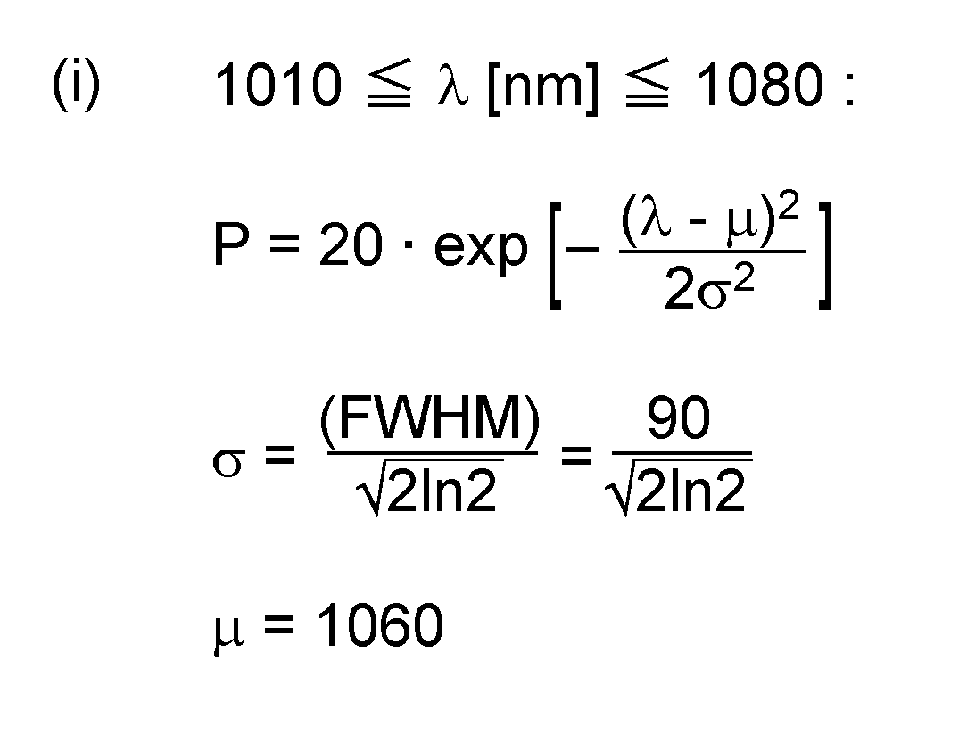
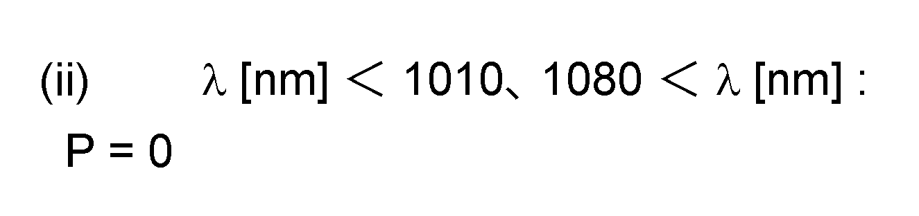
ここで、λ:波長、P:光強度である。
この掃引スペクトルは、入射光における掃引波長範囲(1010~1080nm)においては、中心波長1060nm、中心波長における光強度20mW、半値全幅90nmのガウシアン形状(図5に点線で表示)である。それ以外の波長範囲においては、光強度0mWとした形状である。
また、本実施形態では図2に示すように3電極構成とし、電極領域の区分で利得領域と非利得領域に分けた場合、複数の利得領域はそれぞれ同一のキャリア密度とする。さらに、非利得領域では入射光波長における利得がゼロとなるキャリア密度とする。
SOAにおいて、入射光の掃引スペクトルを目標とする掃引スペクトルとして射出するためには、次の式を満たす状態とする必要がある。

ここで、λ:波長(1010~1080nm)、Pin(λ):波長λにおける入射光強度、Pout(λ):波長λにおける射出光強度とする。
また、g(N、λ):キャリア密度Nのときの波長λにおけるSOAの利得、Lg:SOAの利得領域の合計長さ、Γ:SOAの光導波路における閉じ込め係数である。以下では、Γ=0.03とした計算結果を示す。
本実施形態のSOAの活性層における利得スペクトルを図6に示す。
また、これをもとにして、キャリア密度Nと対象波長範囲において得られる正の利得の総和∫g(N)との関係を求めた(図7)。∫g(N)は、対象波長範囲においてキャリア密度NにおけるSOA自体から発生する利得領域の単位長さあたりのASE光の総量を表す指標として用いている。
たとえば、入射光波長1060nmにおける最適駆動状態の導出方法を以下に示す。
最適駆動状態とは、所望の掃引スペクトルを形成するように、ある波長の入射光(この場合は波長1060nm)を増幅させ、かつASE光を極力低減させる駆動状態を指す。ここでいう駆動状態とは、各電極領域の長さとそれらの電極領域におけるキャリア密度の組み合わせを指す。つまり、利得領域の合計長さ(利得長)とキャリア密度をそれぞれLg、Ng、非利得領域の合計長さ(非利得長)とキャリア密度をそれぞれLa、Naとすると、最適駆動状態を決定するためにはこれら4つの値を決定する必要がある。
まず、最適駆動状態とするためのNg、Naを求める。
波長1060nmにおけるキャリア密度Nと得られる利得g(N、λ=1060)との関係を図8に示す。次にこれをもとにして、g(N、λ=1060)/∫g(N)を計算した結果を図9に示す。g(N、λ)/∫g(N)は、対象波長範囲におけるASE光の総量に対する波長λにおける利得の大きさを表しており、この値が大きいほどASE光の量を抑えながら波長λの入射光を効率よく増幅できることを意味している。図9においてg(N、λ=1060)/∫g(N)の値が最大となるのは、Nが2.2E+18/cm3のときであるので、入射光波長が1060nmのとき、最適駆動状態とするためのNgは2.2E+18/cm3と決定される。一方、最適駆動状態とするためのNaは、波長1060nmにおける利得がゼロとなるキャリア密度とするので、図8よりg(N、λ=1060)=0となる1.8E+18/cm3と決定される。
次に、最適駆動状態とするためのLgを求める。
この長さは式Aに、図4よりPin(λ=1060)=1.55[mW]、図5よりPout(λ=1060)=20[mW]、図6よりg(N=2.2E+18、λ=1060)=597[/cm]、Γ=0.03の値を代入して得られる。その結果、Lg=1429[μm]が導出される。
以上より、入射光波長1060nmにおける最適駆動状態は、Ng=2.2E+18[/cm3]、Na=1.8E+18[/cm3]、Lg=1429[μm]と決定される。
同様にして、対象波長範囲である1010~1080nmに対して最適駆動状態とするためのLg、Ng、Naを求めた結果を図10に示す。基本的には、入射光が長波長であるほど、最適駆動状態とするためのLgは長く、NgとNaは低くなる傾向がある。
本実施形態では電極の数を3つとするので、少なくとも入射光のうち3波長においては最適な利得長とすることができる。たとえば入射光波長1010、1040、1080nmにおいて最適な利得長とするように最適駆動状態を設定することを考える。入射光波長1010、1040、1080nmにおける、最適駆動状態とするためのLgは図10よりそれぞれ、417、920、3630μmである。したがって、第n電極の長さをLnとすると、図3におけるL1、L2、L3を417、504、2709μm(順不同)とすると、組み合わせにより選択した3種類の入射光波長に対してそれぞれ最適駆動状態とするためのLgがとれることになる。そして、La=L1+L2+L3-LgよりLaを決定することができる。
一方、選択した3波長以外の波長においては最適駆動状態とするための利得長をとることができないが、電極長の組み合わせにより最も近くなる組み合わせを考えることで、最適駆動状態に近づけることができる。
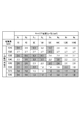
以上より、第n電極領域におけるキャリア密度をNnとしたとき、入射光波長λに対する最適駆動状態とするためのN1、N2、N3、Lgをまとめると図11のようになる。
なお、Ngを黒丸、Naを白丸で各プロット点を示す。
本実施形態の駆動状態におけるSOAと、単電極構成SOAとで、たとえば入射光波長1030、1060nmにおいて最適駆動状態としたg(N、λ)・Lを比較すると、それぞれ図12(a)、(b)のようになる。これより、同じ入射光波長で比較すると、本実施形態の駆動状態におけるSOAの方が単電極構成SOAよりSOA自体から発生するASE光の量を大幅に低減できていることが分かる。
本実施形態では目標とする射出光として、中心波長1060nm、中心波長における光強度20mW、半値全幅90nmのガウシアン形状の掃引スペクトルを想定して計算した例を示している。しかし本実施形態では、中心波長、中心波長における光強度、半値全幅、掃引スペクトル形状はこれに限定されない(矩形形状に関しては実施形態4参照)。
複数の利得領域はそれぞれ同一のキャリア密度とする例を示しているが、それぞれのキャリア密度は同一としなくても効果が得られる範囲が存在する。
非利得領域は入射光波長における利得がゼロとなるキャリア密度とした例を示しているが、入射光波長に対する利得がゼロ以下であれば効果があり、ゼロもしくは逆バイアスで駆動させてもよい。
また、非利得領域のキャリア密度をゼロとする場合、必要でなければ非利得領域と駆動系とを接続しない構成、もしくは非利得領域に電極を形成しない構成としてもよい。
最適駆動状態とする入射光波長を1010、1040、1080nmとした例を示しているが、対象波長範囲内であればこの波長に限定されない。ただし、対象波長範囲内でばらつかせるように設定することが好適構成となる。
電極は3電極構成とした例を示しているが、2つ以上であれば本発明の効果が得られる(2電極構成に関しては実施形態2参照)。
短い長さ(たとえば10μm)の電極を多数配置する構成としてもよい。こうすることで、より最適駆動状態とするための利得長に近づけることが可能となる(利得領域を細かく設定できる電極構成に関しては実施形態3参照)。ただし、この構成とした場合、非電極領域における吸収が大きくなり、電極構成や駆動状態の制御が困難となる場合がある。
本実施形態ではL1=417[μm]、L2=504[μm]、L3=2709[μm]とした例を示したが、電極の長さとその電極のキャリア密度をセットとし、デバイス内でそれぞれ入れ替えても同じ効果が得られる。
本実施形態ではL1=417[μm]、L2=504[μm]、L3=2709[μm]とした例を示したが、たとえば、L1=417[μm]、L2=920[μm]、L3=2293[μm]としても、所望の利得長をとることができる。
電極は3電極構成とした例を示しているが、さらに多い場合でも実質的に同じ駆動状態であれば同じ効果が得られる。例えば、図11の入射光波長1010nmにおける駆動状態(L1=417[μm]、L2=504[μm]、L3=2709[μm]、N1=8.0E+18[/cm3]、N2=N3=3.0E+18[/cm3])を変えても良い。例えば、L1=200[μm]、L2=217[μm]、L3=504[μm]、L4=2709[μm]、N1=N2=8.0E+18[/cm3]、N3=N4=3.0E+18[/cm3]へと変えても、実質的には同じ駆動状態と見なせる。
駆動状態に影響が及ばなければ、Laは長く設計してもかまわない。ただし、長くすると不必要なASE光の量が大きくなるため、極力短くすることが望ましい。
(SOAの利得スペクトルの制御方法)
上記本実施形態に係るSOAと波長掃引光源の別の構成例について説明する。
上記本実施形態に係るSOAと波長掃引光源の別の構成例について説明する。
本構成例ではまず、波長掃引光源102を駆動させ、出射された光をビームスプリッタ(不図示)で分波する。分波された光の一部をモニタ光としてラインセンサ(不図示)で検出し、モニタ光の中心波長に対応する信号を制御部105に送信する。そして、その信号に基づいてSOA104の各電極へ電流を注入する。このような構成により、SOA104を実際に波長掃引光源から射出された光の波長に対応する利得スペクトルに制御できる。
また、あらかじめ、波長掃引光源102のMEMSミラーの変位を制御するための電圧値と発振波長との関係を把握しておく構成としてもよい。すなわち、波長掃引光源102のMEMS駆動を制御する電圧増幅器(不図示)とSOAの電流制御器105に波形発生装置101から同じ信号を送り、SOAを波長掃引光源からの射出光に対応する利得スペクトルとなるよう制御してもよい。
また、波長掃引光源102から射出される光の波長の時間変化と、射出された光の各波長に適した光増幅をするために、SOAに注入する必要がある電流値との対応関係をテーブルとして記憶したメモリ(不図示)を有する構成でもよい。
(光増幅方法)
上記本実施形態に係る光増幅器を用いて入射光を増幅する光増幅方法について説明する。本実施形態に係る光増幅方法は実施形態1で説明したような半導体光増幅器を用いる。具体的には半導体光増幅器を構成する少なくともいずれか一方の電極層は、半導体光増幅器の光の導波路の導波方向に分離された、2つ以上の電極を含む電極群を有するものである。
上記本実施形態に係る光増幅器を用いて入射光を増幅する光増幅方法について説明する。本実施形態に係る光増幅方法は実施形態1で説明したような半導体光増幅器を用いる。具体的には半導体光増幅器を構成する少なくともいずれか一方の電極層は、半導体光増幅器の光の導波路の導波方向に分離された、2つ以上の電極を含む電極群を有するものである。
本実施形態における光増幅方法は、以下の3つの工程を少なくとも有する。
(1)半導体光増幅器へ光を入射させる入射工程。
(2)半導体光増幅器へ入射した入射光の強度を増幅させる増幅工程。
(3)増幅工程で強度が増幅された光を、前記半導体光増幅器から射出させる射出工程。
(3)の増幅工程は、半導体光増幅器の2つ以上の電極を用いて、半導体光増幅器の活性層における複数の異なる領域に独立に電流を注入することで、入射光の波長に応じて、光増幅倍率を変える工程を有する。
(1)半導体光増幅器へ光を入射させる入射工程。
(2)半導体光増幅器へ入射した入射光の強度を増幅させる増幅工程。
(3)増幅工程で強度が増幅された光を、前記半導体光増幅器から射出させる射出工程。
(3)の増幅工程は、半導体光増幅器の2つ以上の電極を用いて、半導体光増幅器の活性層における複数の異なる領域に独立に電流を注入することで、入射光の波長に応じて、光増幅倍率を変える工程を有する。
また、入射光の波長において活性層の利得が正である、導波路内の領域を利得領域、導波路に沿った利得領域の合計長さを利得長と定義する。このとき増幅工程は、入射光の波長に応じて、利得長を変える工程を有することが好ましい。
また、増幅工程は、入射光の波長が短いほど利得長を短くする工程を有することが好ましい。
また、増幅工程は、入射光の波長が短いほど、活性層のキャリア密度が大きくなるように電流を活性層に注入する工程を有する。
また、増幅工程は、入射光の波長が短いほど、利得領域を短くする工程を有する。
(実施形態2)
以下に本発明の実施形態2を示す。
以下に本発明の実施形態2を示す。
本実施形態におけるSOAの素子構成の上面図を図13に示す。本実施形態においては、電極構成および駆動状態を除いて実施形態1と同一である。そのため、実施形態1との差分のみを説明する。
本実施形態では、上部の電極層が2つの電極を含む電極群を有していることを特徴とする。これにより、最適駆動状態の導出と実際の駆動をより簡易に実行することができるようになる。
本実施形態ではたとえば1020、1070nmに対して最適駆動状態にできるように電極の長さを設計することを考える。
実施形態1に示した方法により最適駆動状態を導出し、入射光波長λに対する最適駆動状態とするためのN1、N2、Lgをまとめると図14のようになる。
なお、Ngを黒丸、Naを白丸で各プロット点を示す。ただし、ここで示している電極構成(L1=321[μm]、L2=3309[μm])は1例であり、電極の長さとその電極に対応する駆動状態を入れ替えても同様の効果が得られる。
本実施形態のSOAと単電極構成SOAとで、たとえば入射光波長1030、1060nmにおいて最適駆動状態としたg(N、λ)・Lを比較すると、それぞれ図15(a)、(b)のようになる。これより、同じ入射光波長で比較すると、本実施形態のSOAの方が単電極構成SOAよりSOA自体から発生するASE光の量を大幅に低減できていることが分かる。
(実施形態3)
以下に本発明の実施形態3を示す。
以下に本発明の実施形態3を示す。
本実施形態におけるSOAの素子構成を図16に示す。本実施形態においては、電極構成および駆動状態を除いて実施形態1と同一である。そのため、実施形態1との差分のみを説明する。
本実施形態では、電極の長さを規則的に変化させた電極構成であることを特徴とする。こうすることで、組み合わせによる利得長および非利得長を実施形態1に対してより自由度を高く調整することができるようになる。
実施形態1では、ある入射光波長に対して最適駆動状態とするための利得長がとれるように各電極の長さを設定したが、この構成だとそれら以外の波長においては最適駆動状態とするための利得長とすることができない。本実施形態では対象波長範囲の全ての入射光波長に対して、最適駆動状態とするための利得長により近い長さとなる電極の長さの組み合わせがとれるように電極の長さを設計する。たとえば、Lk=2m・Ll(k、l、m:自然数)を満たす電極をなるべく多くとる構成とする。具体的には図16に示すように、L1~L8を20、40、80、160、320、640、1280、1090μm(順不同)とする。これにより、最適駆動状態とするための利得長が最も大きな値となる入射光波長1080nmにおいて最適駆動状態とするための利得長がとれる構成となる。それに加え、電極の長さの組み合わせにより、各入射光波長における最適駆動状態とするための利得長と、実際の利得長との差を10μm未満に抑えることができるようになる。
実施形態1に示した方法により最適駆動状態を導出し、入射光波長に対する最適駆動状態とするためのそれぞれの電極領域の長さとキャリア密度をまとめると図23のようになる。ただし、ここで示している電極構成(L1=20[μm]、L2=40[μm]、L3=80[μm]、L4=160[μm]、L5=320[μm]、L6=640[μm]、L7=1280[μm]、L8=1090[μm])は1例である。前述の各電極の長さとその電極に対応する駆動状態を入れ替えても同様の効果が得られる。
なお、色を付けたキャリア密度は非利得領域におけるキャリア密度を表す。
本実施形態のSOAと単電極構成SOAとで、たとえば入射光波長1030、1060nmにおいて最適駆動状態としたg(N、λ)・Lを比較すると、それぞれ図17(a)、(b)のようになる。これより、同じ入射光波長で比較すると、本実施形態のSOAの方が単電極構成SOAよりSOA自体から発生するASE光の量を大幅に低減できていることが分かる。
本実施形態では電極の最小単位を20μmとした例を示しているが、10μmや50μmや100μmといった値でも本実施形態と同様の効果が得られる。ただし、10μm未満とした場合、非電極領域における吸収が大きくなり、電極構成や駆動状態の制御が困難となる場合がある。
Lk=2m・Llを満たす電極の長さの組を7とした例を示しているが、1組以上あれば本実施形態と同様の効果が得られる。
(実施形態4)
以下に本発明の実施形態4について説明する。
以下に本発明の実施形態4について説明する。
本実施形態においては、目標とする射出光を除いて実施形態1と同一である。そのため、実施形態1との差分のみを説明する。よって、サンプル構成は図3に示すとおりだが、電極の長さや駆動状態は実施形態1と異なる。
本実施形態における目標とする射出光は、波長1010~1080nmにおいて光強度20mWである矩形形状の掃引スペクトル(図18)を想定している。
最適駆動状態の導出方法は実施形態1に示したとおりである。
本実施形態ではたとえば1010、1040、1080nmに対して最適駆動状態にできるように電極の長さを設計することを考える。
対象波長範囲である1010~1080nmに対して最適駆動状態とするためのLg、Ng、Naを求めた結果を図19に示す。さらに、最適駆動状態を導出し、入射光波長λに対する最適駆動状態とするためのN1、N2、N3、Lgをまとめると図20のようになる。
なお、Ngを黒丸、Naを白丸で各プロット点を示す。ただし、ここで示している電極構成(L1=458[μm]、L2=506[μm]、L3=2878[μm])は1例であり、電極の長さとその電極に対応する駆動状態を入れ替えても同様の効果が得られる。
本実施形態のSOAと単電極構成SOAとで、たとえば入射光波長1030、1060nmにおいて最適駆動状態としたg(N、λ)・Lを比較すると、それぞれ図21(a)、(b)のようになる。これより、同じ入射光波長で比較すると、本実施形態のSOAの方が単電極構成SOAよりSOA自体から発生するASE光の量が少ないことが分かる。
(実施形態5)
以下に本発明の実施形態5を示す。
以下に本発明の実施形態5を示す。
本実施形態の構成について、図22を用いて説明する。本実施形態では、本発明のSOAを用いたOCT装置の例を示す。
OCT装置は、射出される光周波数が掃引される光源部301(MEMS-VCSEL)と、光出力の増大と掃引スペクトル形状制御を行う光増幅器(SOA)302と、その間のアイソレータ303とを有する。そして、干渉光を生成する干渉部304と、干渉光を受光して干渉信号を出力する信号出力部305と、該干渉信号に基づいて物体(被検体)の情報を取得する取得部306とを有している。さらに、OCT装置は、測定アーム(照射光学系)307と参照アーム(参照光学系)308を有している。
干渉部304は、2つのカプラ310、311を有している。まず、カプラ310は光源から射出された光を被検体312へ照射する照射光と参照光とに分岐する。照射光は、測定アーム307を経由して被検体312に照射される。より具体的には、測定アーム307に入射した照射光は偏光コントローラ313で偏光状態を整えられた後、コリメータ314から空間光として射出される。その後、照射光はX軸スキャナ315、Y軸スキャナ316、フォーカスレンズ317を介して被検体312に照射される。
なお、X軸スキャナ315、Y軸スキャナ316は被検体312を照射光で走査する機能を有する走査部である。走査部によって、照射光の被検体312への照射位置が変えられる。そして、被検体312からの後方散乱光(反射光)は、再びフォーカスレンズ317、Y軸スキャナ316、X軸スキャナ315、コリメータ314、偏光コントローラ313を経由して測定アーム307から射出される。そして、カプラ310を経由してカプラ311に入射する。
なお、干渉部304、測定アーム307、参照アーム308とを合わせて干渉光学系と呼ぶことが出来る。図22において干渉光学系は、マッハツェンダー型だが、マイケルソン型であってもよい。
一方、参照光は参照アーム308を経由し、カプラ311に入射する。より具体的には、参照アーム308に入射した参照光は、偏光コントローラ318で偏光状態を整えられた後、コリメータ319から空間光として射出される。その後、参照光は分散補償ガラス320、光路長調整光学系321、分散調整プリズムペア322を通り、コリメータレンズ323を介して光ファイバーに入射され、参照アーム308から射出されてカプラ311に入射する。
カプラ311で測定アーム307を経由した被検体312の反射光と参照アーム308を通った光とが干渉する。そして、その干渉光を信号出力部305で検出する。信号出力部305は、差動検出器324とA/D変換器325を有している。まず、信号出力部305では、カプラ311で干渉光を発生させた後すぐに分波された干渉光を差動検出器324で検出する。そして、差動検出器324で電気信号に変換された干渉信号をA/D変換器325でデジタル信号に変換している。そして、デジタル信号が情報取得部306に送られ、デジタル信号に対してフーリエ変換などの周波数分析が行われることで、被検体312の情報が得られる。得られた被検体312の情報は表示部326によって断層像として表示される。
図22のOCT装置では、干渉光のサンプリングタイミングは、光源の外に設けられるkクロック発生部327が発信するkクロック信号に基づいて等光周波数(等波数)間隔に行われる。
また、光源から射出された光の一部をkクロック発生部327に分岐するために、カプラ309が設けられている。
なお、kクロック発生部327、カプラ309は光源301、またはSOA302に組み込まれていてもよい。
以上は、被検体312のある1点における断層に関する情報の取得のプロセスであり、このように被検体312の奥行き方向の断層に関する情報を取得することをA-scanと呼ぶ。
また、A-scanと直交する方向で被検体312の断層に関する情報、すなわち2次元画像を取得するための走査方向をB-scan、さらにA-scan、およびB-scanのいずれの走査方向とも直交する方向に走査することをC-scanと呼ぶ。これは、3次元断層像を取得する際に眼底面内に2次元ラスター走査する場合、高速な走査方向がB-scan、B-scanをその直交方向に並べて走査する低速な走査方向をC-scanと呼ぶ。A-scan及びB-scanを行うことで2次元の断層像が得られ、A-scan、B-scan及びC-scanを行うことで、3次元の断層像を得ることができる。B-scan、C-scanは、上述したX軸スキャナ315、Y軸スキャナ316により行われる。
なお、X軸スキャナ315、Y軸スキャナ316は、それぞれ回転軸が互いに直交するよう配置された偏向ミラーで構成されている。X軸スキャナ315はX軸方向の走査を行い、Y軸スキャナ316はY軸方向の走査を行う。X軸方向、Y軸方向の各方向は、被検体の表面垂線に対して垂直な方向で、互いに垂直な方向である。
また、B-scan、C-scanのようなライン走査方向と、X軸方向またはY軸方向とは、一致していなくてもよい。このため、B-scan、C-scanのライン走査方向は、撮像したい2次元の断層像あるいは3次元の断層像に応じて、適宜決めることができる。
本実施形態で特徴的なのはSOAであり、上記実施形態で記載した本発明のSOAを用いると、MEMS-VCSELの掃引スペクトル形状を制御しながらASE光を低減できるので、高解像な断層画像情報を取得するのに有利となる。このOCT装置は、主に眼科における断層画像撮影に有用である。
本発明は上記実施の形態に制限されるものではなく、本発明の精神及び範囲から離脱することなく、様々な変更及び変形が可能である。従って、本発明の範囲を公にするために以下の請求項を添付する。
本願は、2016年4月28日提出の日本国特許出願特願2016-091615を基礎として優先権を主張するものであり、その記載内容の全てをここに援用する。
201 入射端面
202 射出端面
203 上部電極層(p電極)
204 下部電極層(n電極)
205 活性層
206 リッジ
207 第1電極領域
208 第2電極領域
209 第3電極領域
210 GaAs基板
211 n型クラッド層
212 p型クラッド層
213 コンタクト層
214 絶縁膜
202 射出端面
203 上部電極層(p電極)
204 下部電極層(n電極)
205 活性層
206 リッジ
207 第1電極領域
208 第2電極領域
209 第3電極領域
210 GaAs基板
211 n型クラッド層
212 p型クラッド層
213 コンタクト層
214 絶縁膜
Claims (17)
- 2つの電極層と、それらの間に設けられた活性層とを含む積層体を有し、
前記積層体は、前記活性層の面内方向に光が導波される導波路を有し、
前記積層体への入射光が、前記導波路を経て、前記積層体の面内方向の端面側から増幅されて射出される光増幅器であって、
前記2つの電極層の少なくともいずれか一方は、前記導波路の導波方向に分離されて設けられた2つ以上の電極を含む電極群を有し、
前記光増幅器は、前記2つ以上の電極を用いて、前記活性層における複数の異なる領域に独立に電流を注入することで、前記入射光の波長に応じて、前記入射光の増幅率を変化させることが可能に構成されている光増幅器。 - 前記2つ以上の電極を用いて、前記活性層における複数の異なる領域に注入される電流を独立に制御する制御部を有する請求項1に記載の光増幅器。
- 前記入射光の波長において前記活性層の利得が正である、前記導波路内の領域を利得領域、前記導波路に沿った利得領域の合計長さを利得長と定義するとき、前記入射光の波長に応じて、前記利得長を変えることが可能に構成されている請求項1または2に記載の光増幅器。
- 前記入射光の波長が短いほど、前記利得長を短くするように構成されている請求項1乃至3のいずれか一項に記載の光増幅器。
- 前記入射光の波長が短いほど、前記活性層に注入される電流の電流密度を大きくするように構成されている請求項1乃至4のいずれか一項に記載の光増幅器。
- 前記入射光の波長が短いほど、前記電極群のうち、前記活性層に電流を注入するために用いられる電極が少なくなるように構成されている請求項1乃至5のいずれか一項に記載の光増幅器。
- 前記光増幅器から射出される光の波長の時間変化の波形が、略ガウシアン形状、略矩形形状、略コサインテーパ形状のいずれかとなるように構成されている請求項1乃至6のいずれか一項に記載の光増幅器。
- 前記活性層が、非対称の量子井戸構造を有する請求項1乃至7のいずれか一項に記載の光増幅器。
- 射出する光の波長を変化させる光源部と、前記光源部から射出された光を増幅する請求項 1乃至8のいずれか一項に記載の光増幅器とを有する光源システム。
- 前記光源部が面発光レーザである請求項9に記載の光源システム。
- 射出する光の波長を変化させる光源部と、
前記光源部から射出された光を増幅する請求項1乃至8のいずれか一項に記載の光増幅器と、
前記光増幅器から射出された光を、照射光学系を通り物体へ照射される照射光と、参照光学系を通る参照光とに分波し、
前記物体に照射された光の反射光と前記参照光による干渉光を発生させる干渉光学系と、
前記干渉光を受光して干渉信号を出力する信号出力部と、
前記干渉信号に基づいて、前記物体の情報を取得する取得部と、
を有する光干渉断層計。 - 前記光源部が面発光レーザである請求項11に記載の光干渉断層計。
- 半導体光増幅器を用いて入射光を増幅する光増幅方法であって、
前記半導体光増幅器を構成する少なくともいずれか一方の電極層は、前記半導体光増幅器の光の導波路の導波方向に分離された、2つ以上の電極を含む電極群を有し、
前記光増幅方法は、
前記半導体光増幅器へ光を入射させる入射工程と
前記半導体光増幅器へ入射した入射光の強度を増幅させる増幅工程と、
前記増幅工程で強度が増幅された光を、前記半導体光増幅器から射出させる射出工程と、を有し、
前記増幅工程は、前記2つ以上の電極を用いて、前記半導体光増幅器の活性層における複数の異なる領域に独立に電流を注入することで、前記入射光の波長に応じて、光増幅倍率を変える工程を有する光増幅方法。 - 前記入射光の波長において前記活性層の利得が正である、前記導波路内の領域を利得領域、前記導波路に沿った利得領域の合計長さを利得長と定義するとき、
前記増幅工程は、前記入射光の波長に応じて、前記利得長を変える工程を有する請求項13に記載の光増幅方法。 - 前記増幅工程は、前記入射光の波長が短いほど前記利得長を短くする工程を有する請求項13または14に記載の光増幅方法。
- 前記増幅工程は、前記入射光の波長が短いほど、前記活性層のキャリア密度が大きくなるように電流を前記活性層に注入する工程を有する請求項13乃至15のいずれか一項に記載の光増幅方法。
- 前記増幅工程は、前記入射光の波長が短いほど、前記利得領域を短くする工程を有する請求項13乃至16のいずれか一項に記載の光増幅方法。
Priority Applications (1)
| Application Number | Priority Date | Filing Date | Title |
|---|---|---|---|
| US16/170,612 US20190059717A1 (en) | 2016-04-28 | 2018-10-25 | Optical amplifier, optical coherence tomography including optical amplifier, and optical amplification method using optical amplifier |
Applications Claiming Priority (2)
| Application Number | Priority Date | Filing Date | Title |
|---|---|---|---|
| JP2016091615A JP2017199877A (ja) | 2016-04-28 | 2016-04-28 | 光増幅器、それを備える光干渉断層計、及び光増幅器を用いた光増幅方法 |
| JP2016-091615 | 2016-04-28 |
Related Child Applications (1)
| Application Number | Title | Priority Date | Filing Date |
|---|---|---|---|
| US16/170,612 Continuation US20190059717A1 (en) | 2016-04-28 | 2018-10-25 | Optical amplifier, optical coherence tomography including optical amplifier, and optical amplification method using optical amplifier |
Publications (1)
| Publication Number | Publication Date |
|---|---|
| WO2017188364A1 true WO2017188364A1 (ja) | 2017-11-02 |
Family
ID=60159954
Family Applications (1)
| Application Number | Title | Priority Date | Filing Date |
|---|---|---|---|
| PCT/JP2017/016689 Ceased WO2017188364A1 (ja) | 2016-04-28 | 2017-04-27 | 光増幅器、それを備える光干渉断層計、及び光増幅器を用いた光増幅方法 |
Country Status (3)
| Country | Link |
|---|---|
| US (1) | US20190059717A1 (ja) |
| JP (1) | JP2017199877A (ja) |
| WO (1) | WO2017188364A1 (ja) |
Cited By (1)
| Publication number | Priority date | Publication date | Assignee | Title |
|---|---|---|---|---|
| CN114764165A (zh) * | 2021-01-15 | 2022-07-19 | 三星电子株式会社 | 光隔离器和包括其的光子集成电路 |
Families Citing this family (1)
| Publication number | Priority date | Publication date | Assignee | Title |
|---|---|---|---|---|
| DE112018004478B4 (de) | 2017-10-13 | 2025-03-27 | Rohm Co., Ltd. | Elektronikkomponente |
Citations (7)
| Publication number | Priority date | Publication date | Assignee | Title |
|---|---|---|---|---|
| JPH0645678A (ja) * | 1992-03-17 | 1994-02-18 | Nec Corp | 半導体光増幅器の光出力パワー一定化方法及び装置 |
| US20030039425A1 (en) * | 2001-08-23 | 2003-02-27 | Robert Stoddard | Integrated optical switch/amplifier with modulation cpabilities |
| JP2003124578A (ja) * | 2001-10-09 | 2003-04-25 | Nippon Telegr & Teleph Corp <Ntt> | 半導体光増幅素子 |
| JP2007184557A (ja) * | 2005-12-05 | 2007-07-19 | Fujifilm Corp | 半導体発光素子および該素子を備えた光源装置および光断層画像化装置 |
| JP2009049280A (ja) * | 2007-08-22 | 2009-03-05 | Sharp Corp | 半導体光増幅素子及び脈波計測装置 |
| JP2014082485A (ja) * | 2012-09-28 | 2014-05-08 | Canon Inc | 光源及び前記光源を用いた光干渉断層撮像装置 |
| JP2016027333A (ja) * | 2014-06-30 | 2016-02-18 | キヤノン株式会社 | 光干渉断層計、面発光レーザ |
-
2016
- 2016-04-28 JP JP2016091615A patent/JP2017199877A/ja active Pending
-
2017
- 2017-04-27 WO PCT/JP2017/016689 patent/WO2017188364A1/ja not_active Ceased
-
2018
- 2018-10-25 US US16/170,612 patent/US20190059717A1/en not_active Abandoned
Patent Citations (7)
| Publication number | Priority date | Publication date | Assignee | Title |
|---|---|---|---|---|
| JPH0645678A (ja) * | 1992-03-17 | 1994-02-18 | Nec Corp | 半導体光増幅器の光出力パワー一定化方法及び装置 |
| US20030039425A1 (en) * | 2001-08-23 | 2003-02-27 | Robert Stoddard | Integrated optical switch/amplifier with modulation cpabilities |
| JP2003124578A (ja) * | 2001-10-09 | 2003-04-25 | Nippon Telegr & Teleph Corp <Ntt> | 半導体光増幅素子 |
| JP2007184557A (ja) * | 2005-12-05 | 2007-07-19 | Fujifilm Corp | 半導体発光素子および該素子を備えた光源装置および光断層画像化装置 |
| JP2009049280A (ja) * | 2007-08-22 | 2009-03-05 | Sharp Corp | 半導体光増幅素子及び脈波計測装置 |
| JP2014082485A (ja) * | 2012-09-28 | 2014-05-08 | Canon Inc | 光源及び前記光源を用いた光干渉断層撮像装置 |
| JP2016027333A (ja) * | 2014-06-30 | 2016-02-18 | キヤノン株式会社 | 光干渉断層計、面発光レーザ |
Cited By (1)
| Publication number | Priority date | Publication date | Assignee | Title |
|---|---|---|---|---|
| CN114764165A (zh) * | 2021-01-15 | 2022-07-19 | 三星电子株式会社 | 光隔离器和包括其的光子集成电路 |
Also Published As
| Publication number | Publication date |
|---|---|
| US20190059717A1 (en) | 2019-02-28 |
| JP2017199877A (ja) | 2017-11-02 |
Similar Documents
| Publication | Publication Date | Title |
|---|---|---|
| USRE41633E1 (en) | Light source for swept source optical coherence tomography based on cascaded distributed feedback lasers with engineered band gaps | |
| JP2017175157A (ja) | 掃引源光干渉断層撮影システム用の波長同調型垂直キャビティ面発光レーザー | |
| JP2009283736A (ja) | 光半導体素子および光半導体素子を用いた光干渉断層画像装置 | |
| JP2015103740A (ja) | 面発光レーザ、およびそれを用いた光干渉断層計 | |
| US7944567B2 (en) | Semiconductor light emitting element, light source using the semiconductor light emitting element, and optical tomography imaging apparatus | |
| JP2009049310A (ja) | 半導体レーザ、バイオイメージングシステム、顕微鏡、光ディスク装置、光ピックアップ、加工装置および内視鏡 | |
| JP2009049123A (ja) | 光半導体素子、該光半導体素子を用いた波長可変光源および光断層画像取得装置 | |
| US20130242310A1 (en) | Light source device including super luminescent diodes, method of driving the same, and optical tomography imaging apparatus | |
| JP2015026645A (ja) | 面発光レーザおよび光干渉断層計 | |
| JP6253326B2 (ja) | 光源及び前記光源を用いた光干渉断層撮像装置 | |
| JP2007184557A (ja) | 半導体発光素子および該素子を備えた光源装置および光断層画像化装置 | |
| US10290994B2 (en) | Laser device, information acquisition device, and imaging system | |
| US20150085295A1 (en) | Light emitting device and optical coherence tomography apparatus including same as light source | |
| US9124070B2 (en) | Superluminescent diode and optical coherence tomography apparatus including the superluminescent diode | |
| WO2017188364A1 (ja) | 光増幅器、それを備える光干渉断層計、及び光増幅器を用いた光増幅方法 | |
| JP2008270585A (ja) | 光半導体素子、該光半導体素子を用いた波長可変光源および光断層画像取得装置 | |
| JP6608203B2 (ja) | 面発光レーザ、情報取得装置及び撮像装置 | |
| JP2015233127A (ja) | 面発光レーザ、レーザアレイ、光源装置、情報取得装置及び光干渉断層計 | |
| JP6282094B2 (ja) | 面発光レーザ、およびそれを用いた光干渉断層計 | |
| JP2008192731A (ja) | 半導体発光素子および該素子を備えた光断層画像化装置 | |
| JP6650961B2 (ja) | 面発光レーザ、およびそれを用いた光干渉断層計 | |
| JP2017098303A (ja) | レーザ装置及び撮像装置 | |
| JP2017143201A (ja) | 光源装置及び情報取得装置 | |
| CN106449898A (zh) | 发光装置及其控制方法和光学相干断层成像设备 | |
| JP2015194496A (ja) | 光源システム、及び前記光源システムを用いた光干渉断層計 |
Legal Events
| Date | Code | Title | Description |
|---|---|---|---|
| NENP | Non-entry into the national phase |
Ref country code: DE |
|
| 121 | Ep: the epo has been informed by wipo that ep was designated in this application |
Ref document number: 17789646 Country of ref document: EP Kind code of ref document: A1 |
|
| 122 | Ep: pct application non-entry in european phase |
Ref document number: 17789646 Country of ref document: EP Kind code of ref document: A1 |