WO2017187971A1 - 放射線検出装置及び放射線検出用信号処理装置 - Google Patents
放射線検出装置及び放射線検出用信号処理装置 Download PDFInfo
- Publication number
- WO2017187971A1 WO2017187971A1 PCT/JP2017/014863 JP2017014863W WO2017187971A1 WO 2017187971 A1 WO2017187971 A1 WO 2017187971A1 JP 2017014863 W JP2017014863 W JP 2017014863W WO 2017187971 A1 WO2017187971 A1 WO 2017187971A1
- Authority
- WO
- WIPO (PCT)
- Prior art keywords
- unit
- reset
- signal
- conversion
- integrated
- Prior art date
- Legal status (The legal status is an assumption and is not a legal conclusion. Google has not performed a legal analysis and makes no representation as to the accuracy of the status listed.)
- Ceased
Links
Images




Classifications
-
- G—PHYSICS
- G01—MEASURING; TESTING
- G01T—MEASUREMENT OF NUCLEAR OR X-RADIATION
- G01T1/00—Measuring X-radiation, gamma radiation, corpuscular radiation, or cosmic radiation
- G01T1/16—Measuring radiation intensity
- G01T1/17—Circuit arrangements not adapted to a particular type of detector
Definitions
- an integrated amount of charge output from a radiation detection unit having a semiconductor radiation detection element such as an SDD (Silicon Drift Detector) is used as a CSA (Charge Sensitive Amplifier).
- CSA Charge Sensitive Amplifier
- an integration signal for example, a voltage signal
- DPP Digital Pulse Processor
- This pulse processor shapes the integrated signal into a pulse signal having a trapezoidal waveform, for example. The peak value of this pulse signal corresponds to the energy of radiation.
- a radiation spectrum can be obtained by counting this pulse signal for each wave height with a counter such as MCA (Multi Channel Analyzer).
- the present invention does not have a configuration in which all the conversion units do not take in the signal from the radiation detection unit every time one of the conversion units is reset as in the synchronous reset method, thereby suppressing an increase in dead time. be able to. Further, since it is detected that any of the conversion units has been reset using the integrated signal from the conversion unit or a signal obtained therefrom, there is no need to acquire reset information from the reset control unit.
- the reset information acquisition unit acquires a reset start point by a change in the integration signal or a signal obtained therefrom
- the noise removal unit is an integration signal from a conversion unit different from the converted conversion unit or It is desirable to remove a signal of a predetermined period determined based on the reset start time from the signal obtained therefrom.
- the reset information acquisition unit acquires a reset end point based on a change in the integration signal or a signal obtained therefrom, and the noise removal unit integrates from a conversion unit different from the reset conversion unit. It is desirable that a signal of a predetermined period determined based on the reset end point is removed from the signal or a signal obtained therefrom. With this configuration, it is only necessary to acquire the reset end point, and it is sufficient to uniformly remove the integration signal for a predetermined period set in advance based on the reset end point or the signal obtained therefrom. Becomes easy. In addition, by acquiring the reset end point, it is possible to prevent the voltage signal after the reset end point from being removed wastefully.
- reset information indicating that any of the conversion units has been reset is acquired and reset using the integrated signals from the plurality of conversion units or signals obtained therefrom. Since the noise caused by reset is removed from the integrated signal from the conversion unit different from the conversion unit or the signal obtained from it, the adverse effect due to crosstalk of the reset signal is reduced and the dead time is increased. Can be suppressed.
- the X-ray detection apparatus 100 of the present embodiment includes a plurality of X-ray detection units 2 that output charges generated by the incidence of X-rays, and a plurality of X-ray detection units 2.
- a plurality of conversion units 3 that are provided corresponding to each of the plurality of conversion units 3 to convert the integrated amount of generated charges into voltage signals that are integration signals corresponding to the integration amount, and process the voltage signals from the plurality of conversion units 3
- a signal processing unit 4 for generating X-ray information.
- the plurality of X-ray detection units 2 have the surface of a single semiconductor block 200 divided into a plurality of X-ray detection regions R1 to R4 and collected in each of the regions R1 to R4.
- the electrodes E1 to E4 are provided to constitute a single detector. That is, the portions corresponding to the X-ray detection regions R1 to R4 are the X-ray detection units 2.
- the collection electrodes E1 to E4 are connected to the output channels Ch1 to Ch4, respectively. Note that the converter 3 is connected to each of the plurality of output channels Ch1 to Ch4.
- Each conversion unit 3 is a charge amplifier (CSA (Charge Sensitive Amplifier)), and the charge output from each X-ray detection unit 2 is integrated and amplified by an operational amplifier 31 and a capacitor 32, and is proportional to the energy of X-rays. The signal is converted into a voltage signal (analog signal).
- Each converter 3 includes an operational amplifier 31, a capacitor 32 connected between the input terminal (inverting input terminal) and the output terminal of the operational amplifier 31, a semiconductor switch (for example, FET) that resets (discharges) the charge of the capacitor 32, and the like. Switch 33.
- CSA Charge Sensitive Amplifier
- the switch 33 is controlled on and off by the reset control unit 5.
- the reset control unit 5 outputs a reset signal for turning on the switch 33 for a predetermined time, and discharges and resets the accumulated charge of the capacitor 32 corresponding to the switch 33.
- a pulse signal (timing pulse) with a small time width is generated.
- the pulse signal with a small time width obtained by the fast system waveform output unit is not only used for pile-up detection, but also output to the reset detection unit 6 to be described later to reset the conversion unit 3. Used for detection.
- the count unit 43 is a multi-channel analyzer (MCA), and is a single unit that processes the peak values obtained by the plurality of peak detectors 42.
- MCA multi-channel analyzer
- the count unit 43 counts the number of times the pulse height of the pulse signal is input for each wave height, and generates an X-ray spectrum that is X-ray information.
- the X-ray detection apparatus 100 uses any pulse signal obtained from the voltage signals from the plurality of conversion units 3, A reset information acquisition unit 6 that acquires reset information indicating that the reset has been performed is provided.
- the reset information acquisition unit 6 receives a pulse signal (output waveform) obtained by the fast waveform output unit of each waveform shaping unit 41, and uses any of the pulse signals to convert any of the conversion units.
- 3 includes a reset information detecting unit 61 that detects reset information indicating that the resetting 3 is reset.
- the conversion unit to which the reset signal is output is also referred to as a reset conversion unit 3A.
- the reset information detection unit 61 compares the pulse signal obtained by the fast waveform output unit of each waveform shaping unit 41 with a predetermined reset detection threshold (for example, a negative value) (FIG. 5C, ( D)). Then, when the output signal falls below a predetermined threshold, the reset information detection unit 61 sets the conversion unit 3 connected to the waveform shaping unit 41 that has output the output signal that has fallen below as the reset conversion unit 3A.
- a predetermined reset detection threshold for example, a negative value
- the reset information detection unit 61 detects the timing when the output signal falls below the predetermined threshold as the reset start time. Further, after detecting the reset start time, the reset information detection unit 61 detects a timing when the pulse signal exceeds the predetermined threshold as a reset end time. Information detected by the reset information detection unit 61 is stored in the reset information storage unit 62. The reset information is stored in the reset information storage unit 62 only by being stored for a short time or being transferred from the reset information detection unit 61 to the signal processing unit 4 (reset information passes). Including. In addition, the reset information acquisition unit 6 outputs a detection signal including information on the reset start point and reset end point to the signal processing unit 4 together with the information on the reset conversion unit 3A.
- the reset information detection unit 61 when the change amount of the pulse signal obtained by the fast waveform output unit (difference between the pulse signal at time t + 1 and the pulse signal at time t) exceeds a predetermined threshold,
- the conversion unit 3 connected to the waveform shaping unit 41 that outputs the pulse signal may be detected as the reset conversion unit 3A.
- the reset information detection unit 61 outputs the voltage signal when the amount of change in the voltage signal output from the conversion unit (difference between the voltage signal at time t + 1 and the voltage signal at time t) exceeds a predetermined threshold.
- the output conversion unit 3 may be detected as the reset conversion unit 3A.
- the signal processing unit 4 of the present embodiment When the signal processing unit 4 of the present embodiment generates the X-ray information using the voltage signal from the conversion unit 3B different from the reset conversion unit 3A, the signal processing unit 4 is caused by the reset signal to the reset conversion unit 3A. Remove crosstalk noise.
- another conversion unit 3B is, for example, a conversion unit (not necessarily one) adjacent to the reset conversion unit 3A. This is because the conversion unit 3B adjacent to the reset conversion unit 3A is considered to be most affected by the crosstalk noise.
- the conversion unit 3B adjacent to the reset conversion unit 3A is a conversion unit connected to the output channel Ch adjacent to the output channel Ch to which the reset conversion unit 3A is connected.
- the signal processing unit 4 includes a noise removing unit 44 that removes noise from the peak value obtained by the wave height detecting unit 42 based on the reset information obtained by the reset information detecting unit 61.
- the noise removing unit 44 removes a signal (peak value) from the other conversion unit 3B that is affected by noise caused by reset. Specifically, the noise removing unit 44 removes the peak value generated by the crosstalk noise from the peak value obtained by the voltage signal from the other conversion unit 3B from the count by the counting unit 43. To do.
- the noise removing unit 44 removes a peak value included in a predetermined period determined based on the reset start time and the reset end time obtained by the reset information detecting unit 61.
- the predetermined period is a period that is set in advance and includes a period from the time when the crosstalk noise occurs at the rising edge of the reset signal to the time when the crosstalk noise generated at the falling edge of the reset signal attenuates to a negligible level. It is.
- the peak value included in the first predetermined period determined based on the reset start point and the peak value included in the second predetermined period determined based on the reset end point are removed.
- Other peak values from which the peak value caused by the crosstalk noise has been removed by the noise removing unit 44 are counted by the counting unit 43.
- the function of the noise removing unit 44 may be provided in the counting unit 43.
- the reset information indicating that any of the conversion units 3 (3A) has been reset using the voltage signals from the plurality of conversion units 3. Since the noise caused by the reset is removed from the voltage signal from the conversion unit 3B different from the conversion unit 3A, the resolution of the X-ray spectrum is reduced due to the crosstalk of the reset signal, or low energy It is possible to prevent a pseudo spectrum from being formed in the region.
- every conversion unit 3A is not configured to take in a signal from the radiation detection unit 2 every time one of the conversion units 3A is reset as in the synchronous reset method, thereby suppressing an increase in dead time. Can do. Furthermore, since it is detected that any of the conversion units 3 has been reset using the voltage signal from the conversion unit 3, there is no need to acquire reset information from the reset control unit 5.
- the present invention is not limited to the above embodiment.
- the signal processing unit of the embodiment is configured to remove noise from the peak value before being input to the counting unit, but in addition, the crosstalk noise is removed as follows. Also good.
- the X-ray detection apparatus 100 detects the delay unit 45 when the delay unit 45 that delays the voltage signal from the conversion unit 3 and the reset conversion unit 3 ⁇ / b> A are detected. And a noise removal unit 46 that removes crosstalk noise from the voltage signal of another conversion unit 3B delayed by 45 based on reset information.
- the X-ray detection apparatus 100 inputs the voltage signal before being delayed to the fast waveform output unit of the waveform shaping unit 41, and the conversion unit 3 ⁇ / b> A reset by the reset information detection unit 61. Is detected (see FIG. 8A).
- the reset information acquisition unit 6 outputs the reset information from the reset information detection unit 61 to a noise removal unit 45 corresponding to another conversion unit 3B, and the noise removal unit 45 includes the delay unit. Crosstalk noise is removed by linear interpolation or the like with values before and after a predetermined removal period from the voltage signal of another conversion unit 3B delayed by 44 (see FIGS. 8C and 8D).
- the voltage signal from which the crosstalk noise has been removed by the noise removal unit 45 is input to the waveform shaping unit 41, and the waveform is shaped by the slow waveform output unit of the waveform shaping unit 41.
- a pulse signal is generated.
- the crest value of the pulse signal is detected by the crest detector 42 and counted by the crest 43 by the crest.
- the noise removing unit 44 is configured to remove the crest values included in each of the first predetermined period and the second predetermined period.
- the noise removing unit 44 is continuous including the reset start time and the reset end time. You may comprise so that the peak value contained in a period may be removed.
- the reset information acquisition unit 6 of the above embodiment may acquire only one of the reset start time and the reset end time.
- the noise removing unit 44 is configured to remove a peak value included in a predetermined period based on the reset start time or a predetermined period based on the reset end time.
- noise removing unit 44 may be provided in the previous stage of the waveform shaping unit 41 or may be provided between the waveform shaping unit 41 and the wave height detection unit 42.
- a plurality of pulse processors (waveform shaping unit and wave height detection unit) are provided corresponding to the plurality of conversion units 3, but a shared pulse processor may be used for the plurality of conversion units 3. good.
- the reset information acquisition unit 6 is common to the plurality of conversion units 3, but a plurality of reset information acquisition units 6 are provided corresponding to the plurality of conversion units 3, respectively. Alternatively, it may be shared by some of the plurality of conversion units 3.
- the converter 3 connected to the output channel Ch which is sufficiently separated from the channel to which the reset converter 3 is connected and the crosstalk noise does not substantially become a problem, and other crosstalk measures such as a shield are provided.
- the conversion unit 3 connected to the existing channel Ch may not perform the crosstalk noise correction process. It should be noted that being sufficiently away from the channel to which the reset conversion unit 3 is connected includes being away from a predetermined distance determined in advance by experiments or the like.
- the crosstalk noise via the output channel of the X-ray detection unit 2 has been described.
- the crosstalk noise via the channel of the signal processing unit 4, the X-ray detection unit, and the conversion unit 3 are mounted. The same applies to the crosstalk between the wirings on the substrate or between the wirings from the substrate to the signal processing unit 4.
- the X-ray detector other semiconductor detectors such as a Si (Li) type detector can be used.
Landscapes
- Physics & Mathematics (AREA)
- Health & Medical Sciences (AREA)
- Life Sciences & Earth Sciences (AREA)
- General Physics & Mathematics (AREA)
- High Energy & Nuclear Physics (AREA)
- Molecular Biology (AREA)
- Spectroscopy & Molecular Physics (AREA)
- Measurement Of Radiation (AREA)
Abstract
本発明は、リセット信号のクロストークによる悪影響を低減するとともに、不感時間(デッドタイム)の増加を抑制するものであり、放射線が入射することにより発生した電荷を出力する複数の放射線検出部2と、複数の放射線検出部2に対応して設けられ、発生した電荷の積算量をその積算量に応じた積算信号に変換する複数の変換部3と、複数の変換部3からの積算信号を処理して放射線情報を生成する信号処理部4と、変換部3にリセット信号を出力して変換部3に蓄積された電荷をリセットするリセット制御部5と、複数の変換部からの積算信号又はそれから得られた信号を用いて、何れかの変換部3がリセットされたことを示すリセット情報を取得するリセット情報取得部6とを備え、信号処理部4は、リセット情報に基づいて、リセットされた変換部3Aとは別の変換部3Bからの積算信号又はそれから得られた信号から、前記リセットに起因するノイズを除去するノイズ除去部44(46)を有する。
Description
本発明は、放射線検出装置及び当該放射線検出装置に用いられる信号処理装置に関するものである。
従来の放射線検出装置としては、特許文献1、2に示すように、SDD(Silicon Drift Detector)等の半導体放射線検出素子を有する放射線検出部から出力される電荷の積算量を、CSA(Charge Sensitive Amplifier)等の変換部によりその積算量に応じた積算信号(例えば電圧信号)に変換して、DPP(Digital Pulse Processor)等のパルスプロセッサに入力する構成とされている。このパルスプロセッサは、積算信号を例えば台形波形からなるパルス信号に整形する。このパルス信号の波高値は、放射線のエネルギーに対応している。そして、このパルス信号をMCA(Multi Channel Analyzer)等のカウンタで波高別にカウントすることによって、放射線スペクトルを得ることができる。
ここで、CSA等の変換部は、放射線検出部から出力される電荷を蓄積するためのコンデンサと、当該コンデンサに蓄積された電荷をリセット(放電)させるためのスイッチとを有している。そして、このスイッチには、コンデンサの電荷が飽和する前の所定のタイミングで外部からリセット信号を入力して、スイッチを所定時間オンにしてコンデンサの電荷をリセットする必要がある。複数の出力チャネルを有する放射線検出部の場合には、当該出力チャネル毎に変換部が設けられているため、各変換部毎にリセットを行う必要がある。
ここで、複数の変換部のコンデンサをリセットする方式として、(1)各コンデンサの蓄積電荷(電圧)が所定値になった時点で、各コンデンサ毎に個別にリセットを行う非同期リセット方式と、(2)何れかのコンデンサの蓄積電荷(電圧)が所定値になった時点で、全ての変換部のコンデンサをリセットするとともに、そのリセット期間において全ての変換部が放射線検出部からの信号を取り込まない同期リセット方式とが考えられている。
しかしながら、非同期リセット方式では、リセットパルスによるクロストークがリセットされていない変換部の出力電圧にノイズとして乗ってしまい、疑似放射線入力パルスとして処理されてしまう。そうすると、放射線スペクトルの分解能を低下させたり、また、低エネルギー領域に疑似スペクトルを形成したりする。
また、同期リセット方式では、何れかのコンデンサをリセットする毎に全ての変換部が放射線検出部からの信号を取り込まないことになり、不感時間(デッドタイム)が増加してしまう。そうすると、マッピングにおいては、全ての変換部において同時に放射線入力処理ができない状況になり、リセット期間に該当する画素で極端に計数率が低下し、ドット抜けのようになってしまう。
そこで本発明は、上記問題点を一挙に解決すべくなされたものであり、リセット信号のクロストークによる悪影響を低減するとともに、不感時間(デッドタイム)の増加を抑制することをその主たる課題とするものである。
すなわち本発明に係る放射線検出装置は、放射線が入射することにより発生した電荷を出力する複数の放射線検出部と、前記複数の放射線検出部に対応して設けられ、前記発生した電荷の積算量をその積算量に応じた積算信号に変換する複数の変換部と、前記複数の変換部からの積算信号を処理して放射線情報を生成する信号処理部と、前記変換部にリセット信号を出力して前記変換部に蓄積された電荷をリセットするリセット制御部と、前記複数の変換部からの積算信号又はそれから得られた信号を用いて、何れかの変換部がリセットされたことを示すリセット情報を取得するリセット情報取得部とを備え、前記信号処理部は、前記リセット情報に基づいて、リセットされた変換部とは異なる変換部からの積算信号又はそれから得られた信号から、前記リセットに起因するノイズを除去するノイズ除去部を有することを特徴とする。
この放射線検出装置によれば、複数の変換部からの積算信号又はそれから得られた信号を用いて、何れかの変換部がリセットされたことを示すリセット情報を取得して、リセットされた変換部とは異なる変換部からの積算信号又はそれから得られた信号からリセットに起因するノイズを除去するので、リセット信号のクロストークにより、放射線スペクトルの分解能を低下させたり、低エネルギー領域に疑似スペクトルを形成したりすることを防止することができる。また、本発明は、同期リセット方式のように何れかの変換部をリセットする毎に全ての変換部が放射線検出部からの信号を取り込なまい構成では無いので、不感時間の増大を抑制することができる。さらに、変換部からの積算信号又はそれから得られた信号を用いて何れかの変換部がリセットされたことを検出しているので、リセット制御部からリセット情報を取得する必要も無い。
前記リセット情報取得部は、前記積算信号又はそれから得られた信号の変化によりリセット開始時点を取得するものであり、前記ノイズ除去部は、リセットされた変換部とは異なる変換部からの積算信号又はそれから得られた信号から、前記リセット開始時点に基づいて定まる所定期間の信号を除去するものであることが望ましい。
この構成であれば、リセット開始時点を取得するだけでよく、当該リセット開始時点に基づいて予め設定された所定期間の積算信号又はそれから得られた信号を画一的に取り除けばよいので、信号処理が容易となる。
この構成であれば、リセット開始時点を取得するだけでよく、当該リセット開始時点に基づいて予め設定された所定期間の積算信号又はそれから得られた信号を画一的に取り除けばよいので、信号処理が容易となる。
また、前記リセット情報取得部は、前記積算信号又はそれから得られた信号の変化によりリセット終了時点を取得するものであり、前記ノイズ除去部は、リセットされた変換部とは異なる変換部からの積算信号又はそれから得られた信号から、前記リセット終了時点に基づいて定まる所定期間の信号を除去するものであることが望ましい。
この構成であれば、リセット終了時点を取得するだけでよく、当該リセット終了時点に基づいて予め設定された所定期間の積算信号又はそれから得られた信号を画一的に取り除けばよいので、信号処理が容易となる。また、リセット終了時点を取得することにより、リセット終了時点後の電圧信号を無駄に取り除くことを防ぐこともできる。
この構成であれば、リセット終了時点を取得するだけでよく、当該リセット終了時点に基づいて予め設定された所定期間の積算信号又はそれから得られた信号を画一的に取り除けばよいので、信号処理が容易となる。また、リセット終了時点を取得することにより、リセット終了時点後の電圧信号を無駄に取り除くことを防ぐこともできる。
信号処理部の具体的な実施の態様としては、前記信号処理部は、前記変換部からの積算信号をパルス信号に整形する波形整形部と、前記波形整形部により整形されたパルス信号の波高値を検出する波高検出部と、前記波高検出部により得られた波高値を、波高別にカウントするカウント部とをさらに備え、前記ノイズ除去部は、前記リセット情報に基づいて、前記波高検出部により得られた波高値からノイズを除去するものであることが望ましい。
また、信号処理部の別の実施の態様としては、前記信号処理部は、前記変換部からの積算信号を所定時間遅延させる遅延部と、前記遅延部により遅延された積算信号をパルス信号に整形する波形整形部と、前記波形整形部により整形されたパルス信号の波高値を検出する波高検出部と、前記波高検出部により得られた波高値を、波高別にカウントするカウント部とをさらに備え、前記ノイズ除去部は、前記リセット情報に基づいて、前記遅延部により遅延された積算信号からクロストークノイズを除去するものであることが望ましい。
前記複数の放射線検出部は、半導体ブロックの表面が複数の放射線検出領域に分割されており、各領域に収集電極が設けられることにより構成されていることが望ましい。
この構成では、半導体ブロックに複数の収集電極が設けられており、リセットパルスのクロストークノイズが乗り易い。そのため、本発明の効果を一層顕著にすることができる。また、半導体ブロックを複数の放射線検出領域に分割することにより、各収集電極当たりの面積が小さくなり、同じドリフト電界を作るのに必要なバイアス電圧を低くできるので、リーク電流を小さくすることができ、信号のS/N比が向上する。
この構成では、半導体ブロックに複数の収集電極が設けられており、リセットパルスのクロストークノイズが乗り易い。そのため、本発明の効果を一層顕著にすることができる。また、半導体ブロックを複数の放射線検出領域に分割することにより、各収集電極当たりの面積が小さくなり、同じドリフト電界を作るのに必要なバイアス電圧を低くできるので、リーク電流を小さくすることができ、信号のS/N比が向上する。
また、本発明に係る放射線検出用信号処理装置は、放射線が入射することにより発生した電荷を出力する複数の放射線検出部に対応して設けられ、前記発生した電荷の積算量をその積算量に応じた積算信号に変換する複数の変換部と、前記複数の変換部から積算信号を処理して放射線情報を生成する信号処理部と、前記変換部にリセット信号を出力して前記変換部に蓄積された電荷をリセットするリセット制御部と、前記複数の変換部からの積算信号又はそれから得られた信号を用いて、何れかの変換部がリセットされたことを示すリセット情報を取得するリセット情報取得部とを備え、前記信号処理部は、前記リセット情報に基づいて、前記リセットに起因するノイズを除去するノイズ除去部を有することを特徴とする。
このように構成した本発明によれば、複数の変換部からの積算信号又はそれから得られた信号を用いて、何れかの変換部がリセットされたことを示すリセット情報を取得して、リセットされた変換部とは異なる変換部からの積算信号又はそれから得られた信号からリセットに起因するノイズを除去するので、リセット信号のクロストークによる悪影響を低減するとともに、不感時間(デッドタイム)の増加を抑制することができる。
100・・・X線検出装置
2 ・・・X線検出部
3 ・・・変換部
4 ・・・信号処理部
44 ・・・ノイズ除去部
46 ・・・ノイズ除去部
5 ・・・リセット制御部
6 ・・・リセット情報取得部
2 ・・・X線検出部
3 ・・・変換部
4 ・・・信号処理部
44 ・・・ノイズ除去部
46 ・・・ノイズ除去部
5 ・・・リセット制御部
6 ・・・リセット情報取得部
以下に本発明に係る放射線検出装置の一態様であるX線検出装置について図面を参照して説明する。
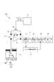
本実施形態のX線検出装置100は、図1及び図2に示すように、X線が入射することにより発生した電荷を出力する複数のX線検出部2と、複数のX線検出部2それぞれに対応して設けられ、発生した電荷の積算量をその積算量に応じた積算信号である電圧信号に変換する複数の変換部3と、複数の変換部3からの電圧信号を処理してX線情報を生成する信号処理部4と、を備えている。
複数のX線検出部2は、シリコンドリフト検出器(SDD(Silicon Drift Detector))である。なお、シリコンドリフト検出器は、同心状の電極構造により中心部の収集電極に発生した電荷を集めるものである。そして、このシリコンドリフト検出器では、入射したX線を空乏層で吸収し、当該空乏層において入射したX線のエネルギーに比例した数の電子-正孔対が生成される。生成された電子は、シリコンドリフト検出器内の電位勾配に従って、発生した電子は収集電極(アノード)に流れる。これにより、シリコンドリフト検出器は、入射したX線のエネルギーに比例した電荷を出力する。
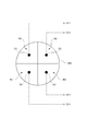
具体的に複数のX線検出部2は、図3に示すように、単一の半導体ブロック200の表面が複数のX線検出領域R1~R4に分割されており、各領域R1~R4に収集電極E1~E4が設けることにより単一の検出器として構成されている。つまり、各X線検出領域R1~R4に対応する部分が各X線検出部2となる。また、収集電極E1~E4は、それぞれ出力チャネルCh1~Ch4に接続されている。なお、複数の出力チャネルCh1~Ch4には、それぞれ変換部3が接続される。
各変換部3は、電荷増幅器(CSA(Charge Sensitive Amplifier))であり、各X線検出部2から出力された電荷をオペアンプ31及びコンデンサ32により積分・増幅して、X線のエネルギーに比例した電圧信号(アナログ信号)に変換するものである。各変換器3は、オペアンプ31と、オペアンプ31の入力端子(反転入力端子)及び出力端子の間に接続されたコンデンサ32と、コンデンサ32の電荷をリセット(放電)させる半導体スイッチ(例えばFET)等のスイッチ33とを有する。
前記スイッチ33は、そのオンオフがリセット制御部5により制御される。
リセット制御部5は、スイッチ33を所定時間オンにするリセット信号を出力して、当該スイッチ33に対応するコンデンサ32の蓄積電荷を放電させてリセットするものである。
リセット制御部5は、スイッチ33を所定時間オンにするリセット信号を出力して、当該スイッチ33に対応するコンデンサ32の蓄積電荷を放電させてリセットするものである。
具体的にリセット制御部5は、各オペアンプ31から出力される電圧信号を取得して、所定のリセット開始閾値と比較し、当該電圧信号がリセット開始閾値を超えた場合に、そのコンデンサ32に対応するスイッチ33にリセット信号を出力して、スイッチ33をオンにする。また、リセット制御部5は、前記電圧信号が所定のリセット終了閾値と比較し、当該電圧信号がリセット終了閾値以下となった場合に、前記スイッチ33をオフにする。あるいは、リセット制御部5は、スイッチ33にリセット信号を出力して所定の一定期間経過した後に、前記スイッチ33をオフにする。なお、各コンデンサ32の電圧を検出する電圧検出手段を設けておき、リセット制御部5は、当該電圧検出手段により得られた電圧が所定の電圧値となったときに、その積分コンデンサ32に対応するスイッチ33にリセット信号を出力するように構成しても良い。その他、リセット制御部5を、各積分コンデンサ32毎に予め設定されたリセット周期毎にリセット信号を出力するように構成しても良い。
ここで、リセット信号は、前記スイッチ33がFETの場合には、そのゲート電圧をゲート閾値電圧(例えば0V)から、ゲート電圧をゲート閾値電圧以上であって所定時間一定電圧とするパルス信号である。
信号処理部4は、変換部3からの電圧信号をパルス信号に整形する波形整形部41と、波形整形部41により整形されたパルス信号の波高値を検出する波高検出部42と、波高検出部42により得られた波高値を、波高別にカウントするカウント部43とを備えている。
波形整形部41及び波高検出部42は、デジタルパルスプロセッサ(DPP(Digital Pulse Processor))であり、複数の変換部3に対応して複数設けられている。
波形整形部41は、変換部3により変換された電圧信号から例えば台形波形のパルス信号(デジタル信号)を生成する。なお、このパルス信号の波高値は、X線のエネルギーに比例している。また、波高検出部42は、ピークホールドにより、入力されたパルス信号の波高値を検出する。
ここで、本実施形態の波形整形部41は、スロー系波形出力部とファスト系波形出力部とを備えている。スロー系波形出力部は、X線のエネルギーに対して高分解能を有するものであり、大きい時定数を用いて、変換部3からの電圧信号をフィルタ処理することにより、時間幅の大きい台形波形のパルス信号を生成するものである。なお、このスロー系波形出力部により得られた時間幅の大きいパルス信号は、波高検出部42及びカウント部43に出力されてX線情報の生成に用いられる。また、ファスト系波形出力部は、X線の入射検出に対して高時間分解能を有するものであり、スロー系波形出力部よりも小さい時定数を用いて、変換部3からの電圧信号をフィルタ処理することにより、時間幅の小さいパルス信号(タイミングパルス)を生成するものである。なお、このファスト系波形出力部により得られた時間幅の小さいパルス信号は、パイルアップの検出等に用いられるだけでなく、後述するリセット検出部6に出力されて、リセットされた変換部3の検出に用いられる。
カウント部43は、マルチチャンネルアナライザ(MCA)であり、複数の波高検出部42により得られた波高値を処理する単一のものである。そして、カウント部43は、波高別に、パルス信号の波高が入力された回数をカウントして、X線情報であるX線スペクトルを生成する。
しかして、本実施形態のX線検出装置100は、図2及び図4に示すように、複数の変換部3からの電圧信号から得られたパルス信号を用いて、何れかの変換部3がリセットされたことを示すリセット情報を取得するリセット情報取得部6を備えている。
リセット情報取得部6は、図4に示すように、各波形整形部41のファスト系波形出力部により得られたパルス信号(出力波形)を受け付けて、それらパルス信号を用いて何れかの変換部3がリセットされたことを示すリセット情報を検出するリセット情報検出部61を有している。以下、リセット信号が出力された変換部をリセット変換部3Aともいう。具体的にリセット情報検出部61は、各波形整形部41のファスト系波形出力部により得られたパルス信号と所定のリセット検出閾値(例えばマイナス値)とを比較する(図5(C)、(D)参照)。そして、リセット情報検出部61は、前記出力信号が所定の閾値を下回った場合に、その下回った出力信号を出力した波形整形部41に接続された変換部3を、リセット変換部3Aとする。
さらにリセット情報検出部61は、図5(D)に示すように、前記出力信号が前記所定の閾値を下回ったタイミングをリセット開始時点として検出する。また、リセット情報検出部61は、前記リセット開始時点を検出した後に、前記パルス信号が前記所定の閾値を上回ったタイミングをリセット終了時点として検出する。これらリセット情報検出部61により検出された情報は、リセット情報格納部62に格納される。なお、リセット情報がリセット情報格納部62に格納されることには、瞬間的な短時間格納されることや、リセット情報検出部61から信号処理部4に受け渡す(リセット情報が通過する)だけのことも含む。また、リセット情報取得部6は、リセット変換部3Aの情報とともに、それらリセット開始時点及びリセット終了時点の情報を含む検出信号を信号処理部4に出力する。
なお、リセット情報検出部61は、ファスト系波形出力部により得られたパルス信号の変化量(時刻t+1のパルス信号と時刻tのパルス信号との差)が所定の閾値を超えた場合に、そのパルス信号を出力した波形整形部41に接続された変換部3を、リセット変換部3Aとして検出しても良い。また、リセット情報検出部61は、変換部から出力される電圧信号の変化量(時刻t+1の電圧信号と時刻tの電圧信号との差)が所定の閾値を超えた場合に、その電圧信号を出力した変換部3を、リセット変換部3Aとして検出しても良い。
そして、本実施形態の信号処理部4は、前記リセット変換部3Aとは別の変換部3Bからの電圧信号を用いてX線情報を生成する場合に、リセット変換部3Aへのリセット信号に起因するクロストークノイズを除去する。
ここで、別の変換部3Bは、例えば、リセット変換部3Aに隣接する変換部(1つとは限らない。)である。なぜならば、リセット変換部3Aに隣接する変換部3Bは、クロストークノイズの影響が最も大きいと考えられるからである。また、リセット変換部3Aに隣接する変換部3Bとは、リセット変換部3Aが接続された出力チャネルChに隣接する出力チャネルChに接続された変換部である。
具体的に信号処理部4は、リセット情報検出部61により得られたリセット情報に基づいて、波高検出部42により得られた波高値からノイズを除去するノイズ除去部44を有している。
このノイズ除去部44は、リセットに伴うノイズの影響を受けている前記別の変換部3Bからの信号(波高値)を除去するものである。具体的にノイズ除去部44は、前記別の変換部3Bからの電圧信号により得られた波高値のうち、クロストークノイズにより生じた波高値を、カウント部43によるカウントから除外するために、除去するものである。
より詳細には、ノイズ除去部44は、前記リセット情報検出部61により得られたリセット開始時点及びリセット終了時点に基づいて定まる所定期間に含まれる波高値を除去する。ここで、所定期間とは、予め設定された期間であり、リセット信号の立ち上がり時にクロストークノイズが生じる時点からリセット信号の立ち下がり時に生じるクロストークノイズが無視できる程度に減衰する時点までを含む期間である。本実施形態では、リセット開始時点に基づいて定まる第1の所定期間に含まれる波高値と、リセット終了時点に基づいて定まる第2の所定期間に含まれる波高値とを除去している。このノイズ除去部44により、クロストークノイズにより生じた波高値が除去されたその他の波高値が、カウント部43によりカウントされる。なお、ノイズ除去部44の機能をカウント部43に持たせても良い。
<本実施形態の効果>
このように構成した本実施形態のX線検出装置100によれば、複数の変換部3からの電圧信号を用いて、何れかの変換部3(3A)がリセットされたことを示すリセット情報を取得して、その変換部3Aとは異なる変換部3Bからの電圧信号からリセットに起因するノイズを除去するので、リセット信号のクロストークにより、X線スペクトルの分解能を低下させたり、また、低エネルギー領域に疑似スペクトルを形成したりすることを防止することができる。また、同期リセット方式のように何れかの変換部3Aをリセットする毎に全ての変換部3が放射線検出部2からの信号を取り込なまい構成では無いので、不感時間の増大を抑制することができる。さらに、変換部3からの電圧信号を用いて何れかの変換部3がリセットされたことを検出しているので、リセット制御部5からリセット情報を取得する必要も無い。
このように構成した本実施形態のX線検出装置100によれば、複数の変換部3からの電圧信号を用いて、何れかの変換部3(3A)がリセットされたことを示すリセット情報を取得して、その変換部3Aとは異なる変換部3Bからの電圧信号からリセットに起因するノイズを除去するので、リセット信号のクロストークにより、X線スペクトルの分解能を低下させたり、また、低エネルギー領域に疑似スペクトルを形成したりすることを防止することができる。また、同期リセット方式のように何れかの変換部3Aをリセットする毎に全ての変換部3が放射線検出部2からの信号を取り込なまい構成では無いので、不感時間の増大を抑制することができる。さらに、変換部3からの電圧信号を用いて何れかの変換部3がリセットされたことを検出しているので、リセット制御部5からリセット情報を取得する必要も無い。
なお、本発明は前記実施形態に限られるものではない。
例えば、前記実施形態の信号処理部は、カウント部に入力される前の波高値からノイズを除去するように構成しているが、その他、次のようにしてクロストークノイズを除去するようにしても良い。
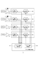
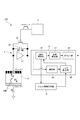
つまり、X線検出装置100は、図6及び図7に示すように、変換部3からの電圧信号を所定時間遅延させる遅延部45と、リセット変換部3Aが検出された場合に、前記遅延部45により遅延された別の変換部3Bの電圧信号からリセット情報に基づいてクロストークノイズを除去するノイズ除去部46とを備えている。
そして、X線検出装置100は、図8に示すように、遅延される前の電圧信号を波形整形部41のファスト系波形出力部に入力し、リセット情報検出部61によりリセットされた変換部3Aを検出する(図8(A)参照)。リセット情報取得部6は、図7に示すように、リセット情報検出部61からのリセット情報を別の変換部3Bに対応するノイズ除去部45に出力し、そのノイズ除去部45は、前記遅延部44により遅延された別の変換部3Bの電圧信号から所定の除去期間の前後の値で直線補間等によりクロストークノイズを除去する(図8(C)、(D)参照)。
このように別の変換部3Bにおいてはノイズ除去部45でクロストークノイズが除去された電圧信号が、波形整形部41に入力されて、当該波形整形部41のスロー系波形出力部により波形整形されてパルス信号が生成される。このパルス信号の波高値が波高検出部42により検出されて、カウント部43により波高別にカウントされる。
前記実施形態では、ノイズ除去部44は第1の所定期間及び第2の所定期間のそれぞれに含まれる波高値を除去するように構成していたが、リセット開始時点及びリセット終了時点を含む連続した期間に含まれる波高値を除去するように構成しても良い。
また、前記実施形態のリセット情報取得部6は、リセット開始時点又はリセット終了時点の一方のみを取得するものであっても良い。この場合、ノイズ除去部44は、リセット開始時点に基づいた所定期間又はリセット終了時点に基づいた所定期間に含まれる波高値を除去するように構成される。
また、ノイズ除去部44は、リセット開始時点に基づいた所定期間又はリセット終了時点に基づいた所定期間に含まれる波高値を除去する他、複数の変換部からの積算信号又はそれから得られた信号と、予め定めた上限閾値及び/又は下限閾値とを比較することによって、それらの大小関係から信号又は波高値をノイズとして除去しても良い。さらに、ノイズ除去部44は、前記所定期間に含まれる信号を除去するだけでなく、その所定期間に含まれる信号のノイズを、実験などにより予め定めた基準値や範囲等を用いてそれらに当てはまるか否かにより特定し、その特定したノイズを除去するようにしても良い。
また、前記実施形態のノイズ除去部44はカウント部43の前段に設けられてカウント部43に入力される波高値からノイズを除去する構成であったが、ノイズ除去部44をカウント部43の後段に設けて、カウント部43により得られたカウント値からノイズによるカウント分を除去するように構成しても良い。具体的は、ノイズ情報取得部6のノイズ情報格納部62により記憶されたリセット開始時点又はリセット終了時点を用いて、そのリセット開始時点又はリセット終了時点に基づいて定まる所定期間にカウントされた値を差し引いて除去することが考えられる。
さらに、ノイズ除去部44は、波形整形部41の前段に設けられたものであっても良いし、波形整形部41及び波高検出部42の間に設けられたものであっても良い。
また、前記実施形態では、波形整形部及び波高検出部をパルスカウンタにより構成し、カウント部をマルチチャネルアナライザにより構成していたが、例えば専用又は汎用のコンピュータ(CPU、メモリ、AD変換器等を有する。)を用いて構成しても良い。
前記実施形態では、複数の変換部3に対応して複数のパルスプロセッサ(波形整形部及び波高検出部)が設けられていたが、複数の変換部3に対して共用のパルスプロセッサを用いても良い。
前記実施形態では、リセット情報取得部6は、複数の変換部3に対して共通のものであったが、リセット情報取得部6は複数の変換部3それぞれに対応して複数設けられるものであっても良いし、複数の変換部3のうちの一部で共用されるものであっても良い。
前記実施形態では、1つのリセット制御部5が複数の変換部3に対してリセット信号を出力する構成であったが、複数の変換部3に対応して複数のリセット制御部5を設ける構成としても良い。
前記実施形態では、リセット変換部3に隣接する変換部3に対してクロストークノイズの補正処理を行うものであったが、それ以外の変換部3に対してクロストークノイズの補正処理を行うものであっても良い。
また、リセット変換部3が接続されるチャネルから十分に離れてクロストークノイズが実質的に問題にならない出力チャネルChに接続される変換部3や、シールド等の他のクロストーク対策が施されているチャネルChに接続される変換部3に対しては、クロストークノイズの補正処理を行わないものであっても良い。なお、上述のリセット変換部3が接続されるチャネルから十分に離れているとは、実験等により予め定められた所定距離離れていることを含む。
さらに、前記実施形態では、X線検出部2の出力チャネルを介したクロストークノイズについて説明したが、信号処理部4のチャネルを介したクロストークノイズ、X線検出部や変換部3を実装している基板の配線間又はその基板から信号処理部4までの配線間でのクロストークについても同様である。
さらに、X線検出器としては、Si(Li)型検出器等のその他の半導体検出器を用いることができる。
その他、本発明は前記実施形態に限られず、その趣旨を逸脱しない範囲で種々の変形が可能であるのは言うまでもない。
本発明によれば、放射線検出装置においてリセット信号のクロストークによる悪影響を低減するとともに、不感時間(デッドタイム)の増加を抑制することができる。
Claims (7)
- 放射線が入射することにより発生した電荷を出力する複数の放射線検出部と、
前記複数の放射線検出部に対応して設けられ、前記発生した電荷の積算量をその積算量に応じた積算信号に変換する複数の変換部と、
前記複数の変換部からの積算信号を処理して放射線情報を生成する信号処理部と、
前記変換部にリセット信号を出力して前記変換部に蓄積された電荷をリセットするリセット制御部と、
前記複数の変換部からの積算信号又はそれから得られた信号を用いて、何れかの変換部がリセットされたことを示すリセット情報を取得するリセット情報取得部とを備え、
前記信号処理部は、前記リセット情報に基づいて、リセットされた変換部とは異なる変換部からの積算信号又はそれから得られた信号から、前記リセットに起因するノイズを除去するノイズ除去部を有する放射線検出装置。 - 前記リセット情報取得部は、前記積算信号又はそれから得られた信号の変化によりリセット開始時点を取得するものであり、
前記ノイズ除去部は、リセットされた変換部とは異なる変換部からの積算信号又はそれから得られた信号から、前記リセット開始時点に基づいて定まる所定期間の信号を除去するものである請求項1記載の放射線検出装置。 - 前記リセット情報取得部は、前記積算信号又はそれから得られた信号の変化によりリセット終了時点を取得するものであり、
前記ノイズ除去部は、リセットされた変換部とは異なる変換部からの積算信号又はそれから得られた信号から、前記リセット終了時点に基づいて定まる所定期間の信号を除去するものである請求項1記載の放射線検出装置。 - 前記信号処理部は、
前記変換部からの積算信号をパルス信号に整形する波形整形部と、
前記波形整形部により整形されたパルス信号の波高値を検出する波高検出部と、
前記波高検出部により得られた波高値を、波高別にカウントするカウント部とをさらに備え、
前記ノイズ除去部は、前記リセット情報に基づいて、前記波高検出部により得られた波高値からノイズを除去するものである請求項2又は3記載の放射線検出装置。 - 前記信号処理部は、
前記変換部からの積算信号を所定時間遅延させる遅延部と、
前記遅延部により遅延された積算信号をパルス信号に整形する波形整形部と、
前記波形整形部により整形されたパルス信号の波高値を検出する波高検出部と、
前記波高検出部により得られた波高値を、波高別にカウントするカウント部とをさらに備え、
前記ノイズ除去部は、前記リセット情報に基づいて、前記遅延部により遅延された積算信号からクロストークノイズを除去するものである請求項2又は3記載の放射線検出装置。 - 前記複数の放射線検出部は、半導体ブロックの表面が複数の放射線検出領域に分割されており、各領域に収集電極が設けられることにより構成されている請求項1記載の放射線検出装置。
- 放射線が入射することにより発生した電荷を出力する複数の放射線検出部に対応して設けられ、前記発生した電荷の積算量をその積算量に応じた積算信号に変換する複数の変換部と、
前記複数の変換部から積算信号を処理して放射線情報を生成する信号処理部と、
前記変換部にリセット信号を出力して前記変換部に蓄積された電荷をリセットするリセット制御部と、
前記複数の変換部からの積算信号又はそれから得られた信号を用いて、何れかの変換部がリセットされたことを示すリセット情報を取得するリセット情報取得部とを備え、
前記信号処理部は、前記リセット情報に基づいて、前記リセットに起因するノイズを除去するノイズ除去部を有する放射線検出用信号処理装置。
Priority Applications (1)
| Application Number | Priority Date | Filing Date | Title |
|---|---|---|---|
| JP2018514249A JP6813572B2 (ja) | 2016-04-28 | 2017-04-11 | 放射線検出装置及び放射線検出用信号処理装置 |
Applications Claiming Priority (2)
| Application Number | Priority Date | Filing Date | Title |
|---|---|---|---|
| JP2016091492 | 2016-04-28 | ||
| JP2016-091492 | 2016-04-28 |
Publications (1)
| Publication Number | Publication Date |
|---|---|
| WO2017187971A1 true WO2017187971A1 (ja) | 2017-11-02 |
Family
ID=60160514
Family Applications (1)
| Application Number | Title | Priority Date | Filing Date |
|---|---|---|---|
| PCT/JP2017/014863 Ceased WO2017187971A1 (ja) | 2016-04-28 | 2017-04-11 | 放射線検出装置及び放射線検出用信号処理装置 |
Country Status (2)
| Country | Link |
|---|---|
| JP (1) | JP6813572B2 (ja) |
| WO (1) | WO2017187971A1 (ja) |
Cited By (2)
| Publication number | Priority date | Publication date | Assignee | Title |
|---|---|---|---|---|
| WO2019117272A1 (ja) * | 2017-12-15 | 2019-06-20 | 株式会社堀場製作所 | シリコンドリフト型放射線検出素子、シリコンドリフト型放射線検出器及び放射線検出装置 |
| WO2020183567A1 (ja) * | 2019-03-11 | 2020-09-17 | オリンパス株式会社 | X線検出装置および蛍光x線分析装置 |
Citations (6)
| Publication number | Priority date | Publication date | Assignee | Title |
|---|---|---|---|---|
| US5393982A (en) * | 1993-05-20 | 1995-02-28 | Princeton Gamma Tech, Inc. | Highly sensitive nuclear spectrometer apparatus and method |
| JPH09197053A (ja) * | 1996-01-05 | 1997-07-31 | Sterling Diagnostic Imaging Inc | 放射線捕捉装置における検出器、検出パネルおよび放射線捕捉方法 |
| JP2002199292A (ja) * | 2000-09-07 | 2002-07-12 | Canon Inc | 信号処理装置及びそれを用いた撮像装置並びに放射線撮像システム |
| JP2010538245A (ja) * | 2007-08-03 | 2010-12-09 | パルセータ,エルエルシー | エネルギー分散型放射線分光分析システムにおけるパイルアップ除去 |
| JP2011247605A (ja) * | 2010-05-24 | 2011-12-08 | Konica Minolta Medical & Graphic Inc | 放射線画像撮影装置および放射線画像処理装置 |
| JP2014003542A (ja) * | 2012-06-20 | 2014-01-09 | Canon Inc | 検出装置、検出システム及び検出装置の駆動方法 |
-
2017
- 2017-04-11 WO PCT/JP2017/014863 patent/WO2017187971A1/ja not_active Ceased
- 2017-04-11 JP JP2018514249A patent/JP6813572B2/ja active Active
Patent Citations (6)
| Publication number | Priority date | Publication date | Assignee | Title |
|---|---|---|---|---|
| US5393982A (en) * | 1993-05-20 | 1995-02-28 | Princeton Gamma Tech, Inc. | Highly sensitive nuclear spectrometer apparatus and method |
| JPH09197053A (ja) * | 1996-01-05 | 1997-07-31 | Sterling Diagnostic Imaging Inc | 放射線捕捉装置における検出器、検出パネルおよび放射線捕捉方法 |
| JP2002199292A (ja) * | 2000-09-07 | 2002-07-12 | Canon Inc | 信号処理装置及びそれを用いた撮像装置並びに放射線撮像システム |
| JP2010538245A (ja) * | 2007-08-03 | 2010-12-09 | パルセータ,エルエルシー | エネルギー分散型放射線分光分析システムにおけるパイルアップ除去 |
| JP2011247605A (ja) * | 2010-05-24 | 2011-12-08 | Konica Minolta Medical & Graphic Inc | 放射線画像撮影装置および放射線画像処理装置 |
| JP2014003542A (ja) * | 2012-06-20 | 2014-01-09 | Canon Inc | 検出装置、検出システム及び検出装置の駆動方法 |
Cited By (4)
| Publication number | Priority date | Publication date | Assignee | Title |
|---|---|---|---|---|
| WO2019117272A1 (ja) * | 2017-12-15 | 2019-06-20 | 株式会社堀場製作所 | シリコンドリフト型放射線検出素子、シリコンドリフト型放射線検出器及び放射線検出装置 |
| CN111373288A (zh) * | 2017-12-15 | 2020-07-03 | 株式会社堀场制作所 | 硅漂移型放射线检测元件、硅漂移型放射线检测器和放射线检测装置 |
| JPWO2019117272A1 (ja) * | 2017-12-15 | 2020-12-17 | 株式会社堀場製作所 | シリコンドリフト型放射線検出素子、シリコンドリフト型放射線検出器及び放射線検出装置 |
| WO2020183567A1 (ja) * | 2019-03-11 | 2020-09-17 | オリンパス株式会社 | X線検出装置および蛍光x線分析装置 |
Also Published As
| Publication number | Publication date |
|---|---|
| JPWO2017187971A1 (ja) | 2019-02-28 |
| JP6813572B2 (ja) | 2021-01-13 |
Similar Documents
| Publication | Publication Date | Title |
|---|---|---|
| US10441238B2 (en) | Radiation imaging apparatus, control method thereof, and program | |
| US10197684B2 (en) | Radiation imaging apparatus, control method thereof, and non-transitory computer-readable storage medium | |
| EP2470927B1 (en) | X-ray detector with integrating readout chip for single photon resolution | |
| US8803064B2 (en) | Signal processing device, including charge injection circuit, and photodetection device | |
| JP6857174B2 (ja) | 放射線検出装置及び放射線検出用信号処理装置 | |
| WO2017081837A1 (en) | Radiation imaging apparatus and photon counting method | |
| US20180063933A1 (en) | Radiation imaging apparatus, radiation imaging system, and exposure control method | |
| JP2011174936A (ja) | 放射線撮像のための撮像素子 | |
| CN113933885A (zh) | 光子计数x射线探测器、医疗成像设备和方法 | |
| JP2014228464A (ja) | 放射線計測装置および放射線計測方法 | |
| US11047996B2 (en) | Photodetector | |
| JP6813572B2 (ja) | 放射線検出装置及び放射線検出用信号処理装置 | |
| JP6598991B2 (ja) | 自動利得切り換えを用いたピクセル検出装置のダイナミックレンジを拡大する方法 | |
| JP6363112B2 (ja) | 放射検出器によって送信される信号を処理するためのデバイス | |
| JP6999593B2 (ja) | 検出装置及びスペクトル生成装置 | |
| JP2020148688A (ja) | 放射線検出装置及び放射線検出用信号処理装置 | |
| JP2021078050A (ja) | 放射線撮像装置および放射線撮像システム | |
| JP6159133B2 (ja) | 放射線検出器、放射線検出方法及びコンピュータプログラム | |
| JP2018141735A (ja) | 電荷検出回路及びそれを含む放射線検出装置 | |
| CN111678593B (zh) | 光子计数装置及光子计数方法 | |
| CN106303311A (zh) | 像素感光值的输出方法 | |
| US10175367B2 (en) | Tool for detecting photon radiation, particularly adapted for high-flux radiation | |
| CN115586561A (zh) | 光子计数探测器系统 | |
| JP2014109550A (ja) | 放射線撮像装置 | |
| WO2016194295A1 (en) | Radiation imaging apparatus, control method thereof, and program |
Legal Events
| Date | Code | Title | Description |
|---|---|---|---|
| WWE | Wipo information: entry into national phase |
Ref document number: 2018514249 Country of ref document: JP |
|
| NENP | Non-entry into the national phase |
Ref country code: DE |
|
| 121 | Ep: the epo has been informed by wipo that ep was designated in this application |
Ref document number: 17789258 Country of ref document: EP Kind code of ref document: A1 |
|
| 122 | Ep: pct application non-entry in european phase |
Ref document number: 17789258 Country of ref document: EP Kind code of ref document: A1 |