WO2017187685A1 - Led用電源装置、および、半導体集積回路 - Google Patents
Led用電源装置、および、半導体集積回路 Download PDFInfo
- Publication number
- WO2017187685A1 WO2017187685A1 PCT/JP2017/002873 JP2017002873W WO2017187685A1 WO 2017187685 A1 WO2017187685 A1 WO 2017187685A1 JP 2017002873 W JP2017002873 W JP 2017002873W WO 2017187685 A1 WO2017187685 A1 WO 2017187685A1
- Authority
- WO
- WIPO (PCT)
- Prior art keywords
- voltage
- rectifying
- output
- signal
- led lamp
- Prior art date
- Legal status (The legal status is an assumption and is not a legal conclusion. Google has not performed a legal analysis and makes no representation as to the accuracy of the status listed.)
- Ceased
Links
Images


Classifications
-
- H—ELECTRICITY
- H05—ELECTRIC TECHNIQUES NOT OTHERWISE PROVIDED FOR
- H05B—ELECTRIC HEATING; ELECTRIC LIGHT SOURCES NOT OTHERWISE PROVIDED FOR; CIRCUIT ARRANGEMENTS FOR ELECTRIC LIGHT SOURCES, IN GENERAL
- H05B47/00—Circuit arrangements for operating light sources in general, i.e. where the type of light source is not relevant
- H05B47/10—Controlling the light source
Definitions
- the present invention relates to an LED power supply device and a semiconductor integrated circuit.
- LED power supply device 100A that controls the dimming rate of the LED lamp X in accordance with the input of a dimming signal (FIG. 3).
- the LED element Xa can be turned off in the energized state where the main power source S1 outputs an AC voltage.
- the above-described conventional LED power supply device 100A requires the auxiliary power supply S2 for supplying power to the control circuit CON that controls the lighting of the LED lamp X via the regulator REG. There was a problem that the manufacturing cost increased.
- the power supply voltage of the control circuit is often about 3.3V to 15V.
- many LED lamps increase the number of LED lamps connected in series to ensure luminance, and are often about 50V to 250V.
- a regulator is required, and there is a problem that a very large power loss and heat generation occur.
- an LED power supply device that can reduce the size of the device and reduce the manufacturing cost by reducing the auxiliary power supply for supplying power to the control circuit that controls the lighting of the LED lamp and the regulator is provided. For the purpose.
- An LED power supply device includes: A primary circuit having a primary coil and outputting an alternating voltage to the primary coil in response to a feedback signal; A first secondary coil that forms a transformer with the primary coil; A second secondary coil that constitutes the transformer together with the primary coil and the first secondary coil; A first rectifying and smoothing circuit connected to the first secondary coil; An LED lamp connected to the first rectifying and smoothing circuit and including one or a plurality of LED elements connected in series; Current detection means provided in the first rectifying / smoothing circuit or between the first rectifying / smoothing circuit and the LED lamp; A second rectifying and smoothing circuit connected to the second secondary coil; Feedback means connected to the second rectifying and smoothing circuit and outputting the feedback signal to the primary circuit based on a detection signal of the current detecting means and an output voltage of the second rectifying and smoothing circuit; A dimming signal that is driven by power supplied from the second rectifying and smoothing circuit and that regulates the dimming rate of the LED lamp output from an external dim
- the control circuit includes: When the dimming signal indicates the lighting of the LED lamp, a control signal is output to the control terminal of the feedback means so that the LED lamp current corresponds to the dimming rate specified by the dimming signal, On the other hand, when the dimming signal indicates that the LED lamp is extinguished, the output voltage of the second rectifying and smoothing circuit is output from the second rectifying and smoothing circuit when the dimming signal indicates that the LED lamp is on.
- a control signal is output to the control terminal of the feedback means so that a first voltage lower than the output voltage is an upper limit value and a second voltage lower than the first voltage is a lower limit value.
- the primary circuit is When the dimming signal indicates lighting of the LED lamp, the AC voltage is output to the primary coil according to the feedback signal so that the LED lamp current corresponds to the dimming rate specified by the dimming signal. And on the other hand, when the dimming signal indicates that the LED lamp is extinguished, the AC voltage is applied to the primary voltage according to the feedback signal so that the LED lamp is extinguished and drivable power is supplied to the control circuit. Output to the side coil.
- the control circuit includes: A dimming circuit that outputs a DC voltage corresponding to a dimming rate specified by the dimming signal; The DC voltage is input to a non-inverting input terminal, the inverting input terminal is connected to the current detection means, and an operational amplifier that outputs a control signal so that the DC voltage and the detection signal are equal, A voltage dividing circuit that outputs a divided voltage obtained by dividing the output voltage of the second rectifying and smoothing circuit; The divided voltage is input to the inverting input terminal, a preset reference voltage is input to the non-inverting input terminal, a control signal is output based on the result of comparing the divided voltage and the reference voltage, and hysteresis characteristics
- a comparator having The control circuit includes: When the dimming signal indicates the lighting of the LED lamp, the control signal output by the operational amplifier is output to the control terminal of the feedback means, When the dimming signal indicates that the LED lamp is turned off, the control signal output by the comparator is output to the control
- the control circuit includes: A first state in which the output of the operational amplifier and the control terminal of the feedback means are conducted when the dimming signal indicates lighting of the LED lamp; and A switching circuit for switching between a second state of conducting the output of the comparator and the control terminal of the feedback means; The dimming circuit controls the operation of the switching circuit.
- the primary circuit is When the dimming signal indicates that the LED lamp is extinguished, the primary side according to the feedback signal so as to be less than the voltage obtained by integrating the forward voltage of the LED element and the number of stages of the LED element of the LED lamp. It is characterized by controlling the AC voltage output to the coil.
- the number of turns of the second secondary coil is smaller than the number of turns of the first secondary coil.
- the feedback means is an insulating signal transmission element that insulates and transmits the feedback signal based on the detected current.
- the feedback means is a light emitting diode.
- the primary side circuit includes a passive element that receives the feedback signal and outputs a reception signal corresponding to the received feedback signal.
- the primary circuit outputs an AC voltage to the primary coil according to the received signal.
- the passive element is a photodiode or a phototransistor.
- the first rectifying / smoothing circuit includes: One end is connected to the other end of the first secondary coil, the other end is connected to the first LED terminal, and the other end of the first secondary coil is directed to the first LED terminal.
- a first rectifying element whose direction is a forward direction;
- a first output capacitor having one end connected to the first LED terminal and the other end connected to the second LED terminal;
- the second rectifying / smoothing circuit includes: One end is connected to the other end of the second secondary coil, the other end is connected to the power supply terminal, and the direction from the other end of the second secondary coil toward the power supply terminal is the forward direction.
- Two rectifying elements And a second output capacitor having one end connected to the power supply terminal and the other end grounded.
- a semiconductor integrated circuit has a primary side coil, and outputs a primary voltage to the primary side coil in response to a feedback signal, the primary side coil, and a transformer Connected to the first secondary coil constituting the transformer, the second secondary coil constituting the transformer together with the primary coil and the first secondary coil, and the first secondary coil.
- a first rectifying / smoothing circuit an LED lamp connected to the first rectifying / smoothing circuit and including one or a plurality of LED elements connected in series, and in the first rectifying / smoothing circuit, or Current detecting means provided between the first rectifying / smoothing circuit and the LED lamp, a second rectifying / smoothing circuit connected to the second secondary coil, and the second rectifying / smoothing circuit Connected to the current detection means.
- the semiconductor integrated circuit is: A dimming signal that is driven by power supplied from the second rectifying and smoothing circuit and that regulates the dimming rate of the LED lamp output from an external dimming unit, a detection signal of the current detection unit, and the first A control signal for controlling the feedback signal to the control terminal of the feedback means according to the output voltage of the rectifying and smoothing circuit of No.
- a control signal is output to the control terminal of the feedback means so that the current of the LED lamp corresponds to the dimming rate specified by the dimming signal
- the dimming signal indicates that the LED lamp is extinguished
- the output voltage of the second rectifying and smoothing circuit is output from the second rectifying and smoothing circuit when the dimming signal indicates that the LED lamp is on.
- the control signal is output to a control terminal of the feedback means so as to be a preset voltage lower than the output voltage to be output.
- An LED power supply device includes a primary side coil that includes a primary side coil and outputs an AC voltage to the primary side coil in response to a feedback signal, and a primary side coil and a transformer that form a first transformer.
- the control circuit when the dimming signal indicates the lighting of the LED lamp, the control circuit outputs the control signal to the control terminal of the feedback means so that the current of the LED lamp corresponds to the dimming rate specified by the dimming signal.
- the dimming signal indicates that the LED lamp is extinguished
- the output voltage of the second rectifying and smoothing circuit is output from the second rectifying and smoothing circuit when the dimming signal indicates that the LED lamp is on.
- a control signal is output to the control terminal of the feedback means so as to be a preset voltage lower than the output voltage.
- the LED lamp is extinguished and drivable power is supplied to the control circuit from the primary side circuit.
- the LED power supply device reduces the auxiliary power supply for supplying power to the control circuit that controls the lighting of the LED lamp, thereby reducing the size and manufacturing cost of the device. Reduction can be achieved.
- FIG. 1 is a diagram illustrating an example of a configuration of an LED power supply device 100 according to the first embodiment.
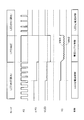
- FIG. 2 is a waveform diagram showing an example of operation waveforms for switching between LED lighting and LED extinguishing of the LED power supply device 100 shown in FIG.
- FIG. 3 is a diagram illustrating an example of the configuration of a conventional LED power supply device 100A.
- FIG. 1 is a diagram illustrating an example of the configuration of the LED power supply device 100 according to the first embodiment.
- the LED power supply device 100 includes, for example, a primary circuit FC1, an LED lamp X, a first LED terminal TX1, a second LED terminal TX2, and a first LED Secondary coil L2a, second secondary coil L2b, first rectifying / smoothing circuit A1, second rectifying / smoothing circuit A2, current detecting means RX, feedback means YA, and amplifier capacitor C And a control resistor R and a control circuit (semiconductor integrated circuit) CON.
- the first LED terminal TX1 is connected to the anode side of the LED lamp X including one or a plurality of LED elements XA connected in series.
- the second LED terminal TX2 is connected to the cathode side of the LED lamp X.
- the first secondary coil L2a constitutes a transformer Z together with the primary coil L1 and the second secondary coil L2b.
- the LED lamp X includes one or a plurality of LED elements XA connected in series.
- the primary side circuit FC1 includes a primary side coil L1 and an AC power source S.
- the primary side circuit FC1 outputs an AC voltage generated from the AC power source S to the primary side coil L1 in response to the feedback signal FBS.
- the primary circuit FC1 includes a passive element YB that receives the feedback signal FBS and outputs a reception signal corresponding to the received feedback signal FBS.
- the primary circuit FC1 outputs an alternating voltage to the primary coil L1 in accordance with the received signal.
- the passive element YB is, for example, a photodiode or a phototransistor.
- the primary side circuit FC1 applies an AC voltage to the primary side coil in accordance with the feedback signal FBS so that a constant current that can be turned on flows through the LED lamp X. It outputs to L1.
- the primary side circuit FC1 provides the feedback signal FBS with a current of the LED lamp X corresponding to the dimming rate specified by the dimming signal AS. Accordingly, an AC voltage is output to the primary coil L1.
- the primary side circuit FC1 supplies the AC voltage to the primary side so that the LED lamp X is extinguished and drivable power is supplied to the control circuit CON. It outputs to the coil L1.
- the primary side circuit FC1 when the dimming signal AS indicates that the LED lamp X is extinguished, the primary side circuit FC1 outputs the feedback signal FBS so that the LED lamp X is extinguished and drivable power is supplied to the control circuit CON. Accordingly, an AC voltage is output to the primary coil L1.
- the primary side circuit FC1 integrates the forward voltage of the LED element XA and the number of stages of the LED element XA of the LED lamp X.
- the AC voltage output to the primary coil L1 is controlled in accordance with the feedback signal FBS so as to be less than the value.
- the first rectifying / smoothing circuit A1 is connected to the first secondary coil L2a and the first rectifying / smoothing circuit A1, for example, as shown in FIG.
- the first rectifying / smoothing circuit A1 rectifies the induced voltage of the first secondary coil L2a and supplies it to the LED lamp X via the first and second LED terminals TX1, TX2. ing.
- the first rectifying / smoothing circuit A1 includes, for example, a first rectifying element (diode) D1, a first output capacitor C1, and a current detecting means RX as shown in FIG.
- the first rectifying element D1 has one end (anode) connected to the other end of the first secondary coil L2a and the other end (cathode) connected to the first LED terminal TX1.
- the diode is connected and has a forward direction from the other end of the first secondary coil L2a toward the first LED terminal TX1.
- the first output capacitor C1 has one end connected to the first LED terminal TX1 and the other end connected to the second LED terminal TX2.
- the second secondary coil L2b constitutes the transformer Z together with the primary coil L1 and the first secondary coil L2a.
- the second secondary coil L2b is set so that the induced electromotive force is smaller than the induced electromotive force of the first secondary coil L2a.
- the number of turns of the second secondary coil L2b is set to be smaller than the number of turns of the first secondary coil L2a.
- the number of turns of the second secondary coil L2b is set to be smaller than the number of turns of the first secondary coil L2a.
- the current detection means RX is a current detection resistor having one end connected to the second LED terminal TX2 and the other end connected to one end of the first secondary coil L2a. is there. In the example shown in FIG. 1, it is provided in the first rectifying / smoothing circuit A1. However, the current detection means RX may be provided between the output of the first rectifying / smoothing circuit A1 and the LED lamp X.
- the current detection means RX outputs a detection signal SRX corresponding to the current flowing through one end.
- the second rectifying / smoothing circuit A2 is connected to the second secondary coil L2b.
- the second rectifying / smoothing circuit A2 supplies an output voltage VC obtained by rectifying the induced voltage of the second secondary coil L2b to the control circuit CON via the power supply terminal TS.
- the second rectifying / smoothing circuit A2 includes, for example, a second rectifying element D2 and a second output capacitor C2, as shown in FIG.
- the second rectifying element D2 has one end (anode) connected to the other end of the second secondary coil L2b and the other end (cathode) connected to the power supply terminal TS.
- the diode is such that the direction from the other end of the second secondary coil L2b toward the power supply terminal TS is the forward direction.
- the second output capacitor C2 has one end connected to the power supply terminal TS and the other end grounded (connected to the ground terminal TGND).
- the feedback means YA is connected to the output of the second rectifying / smoothing circuit A2.
- the feedback means YA is connected between the power supply terminal VC (output of the second rectifying / smoothing circuit A2) and the signal terminal TOUT, for example, as shown in FIG.
- the feedback means YA outputs a feedback signal FBS to the primary side circuit FC1 based on the flowing current.
- the feedback means YA is based on the detection signal SRX of the current detection means RX and the output voltage VC of the second rectifying / smoothing circuit A2 (as described later, the control circuit CON outputs via the signal terminal TOUT. Based on the control signal, the feedback signal FBS is output to the primary circuit FC1.
- This feedback means YA is an insulating signal transmission element that insulates and transmits the feedback signal FBS based on the detection signal SRX of the current detection means RX and the output voltage VC of the second rectifying and smoothing circuit A2. More specifically, as shown in FIG. 1, for example, the feedback means YA has an anode connected to the power supply terminal TS and a cathode connected to the signal terminal TOUT (one end of the current detection means RX via an amplifier capacitor C described later). To) the connected light emitting diode.
- the cathode of this light emitting diode corresponds to the control terminal TYA.
- the control circuit CON supplies a control signal to the control terminal TYA, whereby the feedback signal FBS is controlled.
- the amplifier capacitor C is connected between the control terminal TYA (signal terminal TOUT) and the inverting input terminal (signal terminal TOP) of the operational amplifier OPA.
- the control resistor R is connected between the power supply terminal TS (the output of the second rectifying and smoothing circuit A2) and the feedback means YA (the anode of the light emitting diode).
- control circuit CON is driven by the power (output voltage VC) supplied from the second rectifying / smoothing circuit A2 via the power supply terminal TS.
- the control circuit CON is supplied with a dimming signal AS that regulates the dimming rate of the LED lamp X output from an external dimming means (not shown) via the input terminal TIN, and is detected by the current detection means RX.
- the signal SRX is supplied via the signal terminal TOP, and the output voltage (power supply voltage) VC of the second rectifying / smoothing circuit A2 is supplied via the power supply terminal TS.
- the control circuit CON supplies a control signal SC for controlling the feedback signal FBS to the control terminal TYA of the feedback means YA via the signal terminal TOUT according to the dimming signal AS, the detection signal SRX, and the output voltage VC. It is designed to output.
- the control circuit CON feeds back the control signal so that the current of the LED lamp X corresponds to the dimming rate specified by the dimming signal AS.
- the feedback means YA outputs a feedback signal FBS indicating the lighting of the LED lamp X to the primary side circuit FC1.
- the dimming signal AS indicates the lighting of the LED lamp X
- a constant current is applied to the LED lamp X via the first secondary coil L2a so that the LED lamp X is lit from the primary circuit FC1.
- a driving power supply voltage is supplied to the control circuit CON via the second secondary coil L2b.
- the control circuit CON determines that the output voltage VC of the second rectifying and smoothing circuit A2 is when the dimming signal AS indicates that the LED lamp X is on.
- a control signal is output to the feedback means YA so as to be a preset voltage lower than the output voltage output from the second rectifying / smoothing circuit A2.
- the control circuit CON determines that the output voltage of the second rectifying / smoothing circuit A2 indicates that the dimming signal AS is lit on the LED lamp X. Control so that the first voltage Vth1 lower than the output voltage output from the second rectifying and smoothing circuit A2 is the upper limit and the second voltage Vth2 lower than the first voltage Vth1 is the lower limit.
- the signal is output to the control terminal TYA of the feedback means YA.
- the feedback means YA outputs a feedback signal FBS indicating that the LED lamp X is turned off.
- the primary circuit FC1 integrates the forward voltage of the LED element XA and the number of stages of the LED element XA of the LED lamp X in accordance with the feedback signal FBS indicating that the LED lamp X is turned off.
- the AC voltage output to the primary coil L1 is controlled so as to be less than the voltage (turns off the light).
- the output voltage VC of the second rectifying and smoothing circuit A2 is the output voltage VC output from the second rectifying and smoothing circuit A2 when the dimming signal AS indicates the lighting of the LED lamp X.
- the first voltage Vth1 lower than the first voltage Vth1 is set as the upper limit value
- the second voltage Vth2 lower than the first voltage Vth1 is set as the lower limit value (voltage ripple control).
- the output voltage VC controlled between the first voltage Vth1 and the second voltage Vth2 is supplied to the control circuit CON. That is, when the dimming signal AS indicates that the LED lamp X is extinguished, the primary side circuit FC1 supplies the control circuit CON with power that can be driven and the LED lamp X is extinguished.
- control circuit CON includes a dimming circuit AC, an operational amplifier OPA, a comparator COMP, a voltage dividing circuit RD, a switching circuit SW, and an internal power supply SX.
- the dimming circuit AC outputs a DC voltage corresponding to the dimming rate defined by the dimming signal AS.
- the operational amplifier OPA In the operational amplifier OPA, a DC voltage is input to the non-inverting input terminal, the inverting input terminal is connected to one end of the current detection means RX, and the detection signal SRX is input.
- the operational amplifier OPA outputs a control signal to the control terminal TYA via the switching circuit SW and the signal terminal TOUT so that the DC voltage VA is equal to the average value of the detection signal SRX.
- the voltage dividing circuit RD outputs a divided voltage VD obtained by dividing the output voltage (power supply voltage) VC output from the second rectifying and smoothing circuit A2.
- the voltage dividing circuit RD has one end connected to the power supply terminal TS, the other end grounded (connected to the ground terminal TGND), and a divided voltage obtained by dividing the output voltage VC. It is designed to output.
- the voltage dividing circuit RD includes a first voltage dividing resistor RD1 having one end connected to the output of the second rectifying / smoothing circuit A2 through a power supply terminal TS, and one end having a first end. And a second voltage dividing resistor RD2 connected to the other end of the voltage dividing resistor RD1 and having the other end connected to the ground terminal TGND.
- the voltage dividing resistor RD outputs a voltage between the other end of the first voltage dividing resistor RD1 and one end of the second voltage dividing resistor RD2 as a divided voltage VD.
- the comparator COMP receives a divided voltage VD at its inverting input terminal and a preset reference voltage VB at its non-inverting input terminal, and controls the control signal based on the result of comparing the divided voltage VD and the reference voltage VB ( Voltage).
- This comparator COMP has a hysteresis characteristic.
- the reference voltage VB is output from the reference power supply B.
- the switching circuit SW also includes a first state in which the output of the operational amplifier and the control terminal TYA (signal terminal TOUT) of the feedback means YA are conducted when the dimming signal AS indicates the lighting of the LED lamp X, and the dimming When the signal AS indicates that the LED lamp X is extinguished, the second state in which the output of the comparator and the control terminal TYA (signal terminal TOUT) of the feedback means YA are conducted is switched.
- the dimming circuit AC controls the operation of the switching circuit SW (switching between the first state and the second state) in accordance with the dimming signal AS.
- control circuit CON outputs the control signal output from the operational amplifier OPA to the control terminal TYA in the first state of the switching circuit SW described above.
- the control circuit CON when the dimming signal AS indicates the lighting of the LED lamp X, the control circuit CON outputs the control signal output from the operational amplifier OPA to the control terminal TYA of the feedback means YA via the signal terminal TOUT. .
- control circuit CON outputs the control signal SC to the control terminal (cathode) TYA of the feedback means YA so that the current of the LED lamp X corresponds to the dimming rate specified by the dimming signal AS.
- control circuit CON outputs the voltage output from the comparator COPM to the control terminal TYA in the second state of the switching circuit SW described above.
- the control circuit CON outputs the voltage output by the comparator COMP to the control terminal TYA of the feedback means YA.
- control circuit CON becomes less than the voltage obtained by integrating the forward voltage of the LED element XA and the number of stages of the LED element XA of the LED lamp X (turns off), and the output voltage VC supplied to the control circuit CON is the first voltage
- the control signal SC is output to the control terminal (cathode) TYA of the feedback means YA so that the first voltage Vth1 becomes the upper limit value and the second voltage Vth2 becomes the lower limit value.
- the internal power supply SX supplies a voltage based on the output voltage VC supplied to the power supply terminal TS to each component of the control circuit CON.
- FIG. 2 is a waveform diagram showing an example of operation waveforms for switching between turning on and off the LED power supply device 100 shown in FIG.
- the control circuit CON responds to the on-duty of the dimming signal AS (DC voltage VA output from the dimming circuit AC).
- the switching circuit SW is set to the first state, and the control signal output from the operational amplifier OPA is output to the control terminal TYA.
- the feedback means YA outputs a feedback signal FBS indicating the lighting of the LED lamp X to the primary side circuit FC1.
- the primary side circuit FC1 outputs an AC voltage to the primary side coil L1 so that a constant current that can be lit on the LED lamp X flows according to the feedback signal FBS.
- the current ILED of the LED lamp X flows according to the on-duty of the dimming signal AS, that is, the dimming rate specified by the dimming signal AS.
- the LED voltage VLED of the LED lamp X corresponding to the dimming rate specified by the dimming signal AS is obtained.
- the output voltage VC output from the second rectifying / smoothing circuit A2 changes so as to correlate with the LED voltage VLED.
- the control circuit CON sets the switching circuit SW to the second state, and the control signal output from the comparator COMP is the control terminal. Output to TYA.
- the feedback means YA outputs a feedback signal FBS indicating that the LED lamp X is turned off.
- the primary side circuit FC1 is less than a voltage obtained by integrating the forward voltage of the LED element XA and the number of stages of the LED element XA of the LED lamp X in accordance with the feedback signal FBS indicating that the LED lamp X is turned off.
- the AC voltage output to the primary side coil L1 is controlled (to turn off the light).
- the output voltage VC of the second rectifying and smoothing circuit A2 is the output voltage VC output from the second rectifying and smoothing circuit A2 when the dimming signal AS indicates the lighting of the LED lamp X.
- the first voltage Vth1 lower than the first voltage Vth1 is set as the upper limit value
- the second voltage Vth2 lower than the first voltage Vth1 is set as the lower limit value (voltage ripple control).
- the LED power supply device 100 does not require an auxiliary power supply for supplying power to the control circuit CON that controls the lighting of the LED lamp X.
- the primary side circuit FC1 that includes the primary side coil L1 and outputs an AC voltage to the primary side coil L1 according to the feedback signal FBS, and the primary side A first secondary coil L2a constituting the coil L1 and the transformer Z; a second secondary coil L2b whose induced electromotive force is smaller than the induced electromotive force of the first secondary coil L2a; A first rectifying / smoothing circuit A1 connected to the secondary coil L2a, and an LED lamp X including a plurality of LED elements XA connected to the first rectifying / smoothing circuit A1 and connected in series, The second rectifying / smoothing connected to the current detection means RX included in the first rectifying / smoothing circuit A1 or between the first rectifying / smoothing circuit A1 and the LED lamp X and the second secondary coil L2b.
- Circuit A2 and second Feedback means YA connected to the rectifying / smoothing circuit A2 and outputting the feedback signal FBS to the primary circuit FC1 based on the detection signal of the current detecting means RX and the output voltage of the second rectifying / smoothing circuit A2, and a second Driven by the electric power supplied from the rectifying / smoothing circuit A2, and according to the dimming signal AS that regulates the dimming rate of the LED lamp X, the detection signal of the current detecting means RX, and the output voltage of the second rectifying / smoothing circuit A2.
- a control circuit CON that outputs a signal to the feedback means YA.
- the control circuit CON feeds back the control signal so that the current of the LED lamp X corresponds to the dimming rate specified by the dimming signal AS.
- the control signal is output so that the output voltage of the second rectifying and smoothing circuit A2 becomes a preset voltage. Output to the control terminal TYA of the feedback means YA (ripple control).
- the dimming signal AS indicates the lighting of the LED lamp X
- a constant current is applied to the LED lamp X via the first secondary coil L2a so that the LED lamp X is lit from the primary circuit FC1.
- a power supply voltage for driving is supplied to the control circuit CON via the second secondary coil L2b.
- the primary circuit FC1 extinguishes the LED lamp X and supplies drivable power to the control circuit CON.
- the LED power supply device reduces the auxiliary power supply for supplying power to the control circuit CON that controls the lighting of the LED lamp X, thereby reducing the size and manufacturing of the device. Cost can be reduced.
- LED power supply device FC1 primary side circuit X LED lamp TX1 first LED terminal TX2 second LED terminal L2a first secondary coil L2b second secondary coil A1 first rectifying and smoothing circuit A2 second Rectifying and smoothing circuit RX Current detecting means YA Feedback means C Capacitor for amplifier R Control resistor CON Control circuit (semiconductor integrated circuit) AC dimmer circuit OPA operational amplifier COMP comparator RD voltage divider circuit SW switching circuit SX internal power supply
Landscapes
- Circuit Arrangement For Electric Light Sources In General (AREA)
Abstract
【課題】LEDランプの点灯を制御する制御回路に電源を供給するための補助電源を削減して、装置の小型化や製造コストの低減を図ることが可能なLED用電源装置を提供する。 【解決手段】LED用電源装置の制御回路は、調光信号がLEDランプの点灯を示す場合には、調光信号が規定する調光率に応じたLEDランプの電流になるように制御信号をフィードバック手段の制御端子に出力し、一方、調光信号がLEDランプの消灯を示す場合には、第2の整流平滑回路の出力電圧が、調光信号がLEDランプ点灯を示す場合に第2の整流平滑回路から出力される出力電圧よりも低い予め設定された電圧になるように、制御信号を前記フィードバック手段の制御端子に出力する。
Description
本発明は、LED用電源装置、および、半導体集積回路に関する発明である。
従来、調光信号の入力に応じて、LEDランプXの調光率を制御するLED用電源装置100Aがある(図3)。
このようなLED用電源装置100Aとして、LED素子Xaで構成されるLEDランプXを消灯する場合、LEDの電流値を定電流制御しているため、電流値を0Aに制御するには、主電源S1を停止しなければならず、消灯制御するには、補助電源S2が必要であった。それを解決する手法が、特許文献1に示されている。LEDランプXを消灯する場合は、基準値として予め設定されるLED素子Xaの点灯開始電圧より低い電圧値と、LEDランプXの電圧を検出する検出手段RXaの検出信号との比較結果に基づいて、LED素子Xaに印加される電圧を点灯開始電圧よりも低い一定電圧にする。
これにより、主電源S1が交流電圧を出力する通電状態で、LED素子Xaを消灯状態にすることができる。
しかし、既述の従来のLED用電源装置100Aでは、LEDランプXの点灯を制御する制御回路CONにレギュレータREGを介して電力を供給するための補助電源S2が必要になり、装置の大型化や製造コストが増加する問題があった。
また、特許文献1の回路では、制御回路の電源電圧は、3.3V~15V程度である事が多い。しかし、LEDランプについては、LEDランプを直列に接続する数を増やして、輝度を確保するものが多く、50V~250V程度の電圧である事も多い。50V~250Vの出力から3.3V~15Vの電圧を得るにはレギュレータが必要であり、且つ非常に大きな電力損失、発熱が発生するという問題があった。
そこで、LEDランプの点灯を制御する制御回路に電源を供給するための補助電源や、レギュレータを削減して、装置の小型化や製造コストの低減を図ることが可能なLED用電源装置を提供することを目的とする。
本発明の一態様に係る実施例に従ったLED用電源装置は、
一次側コイルを有し、フィードバック信号に応じて前記一次側コイルに交流電圧を出力する一次側回路と、
前記一次側コイルとトランスを構成する第1の二次側コイルと、
前記一次側コイルと前記第1の二次側コイルとともに前記トランスを構成する第2の二次側コイルと、
前記第1の二次側コイルと接続される第1の整流平滑回路と、
前記第1の整流平滑回路と接続され、1つ又は直列に接続された複数のLED素子を含むLEDランプと、
前記第1の整流平滑回路内、又は、前記第1の整流平滑回路と前記LEDランプとの間に設けられた電流検出手段と、
前記第2の二次側コイルと接続された第2の整流平滑回路と、
前記第2の整流平滑回路と接続され、前記電流検出手段の検出信号、及び、第2の整流平滑回路の出力電圧に基づいて前記フィードバック信号を前記一次側回路に出力するフィードバック手段と、
前記第2の整流平滑回路から供給される電力により駆動し、外部の調光手段から出力される前記LEDランプの調光率を規定する調光信号、前記電流検出手段の検出信号、及び前記第2の整流平滑回路の出力電圧に応じて、前記フィードバック手段の制御端子に前記フィードバック信号を制御するための制御信号を出力する制御回路と、を備え、
前記制御回路は、
前記調光信号がLEDランプの点灯を示す場合には、前記調光信号が規定する調光率に応じたLEDランプの電流になるように制御信号を前記フィードバック手段の制御端子に出力し、
一方、前記調光信号がLEDランプの消灯を示す場合には、前記第2の整流平滑回路の出力電圧が、前記調光信号がLEDランプ点灯を示す場合に前記第2の整流平滑回路から出力される出力電圧よりも低い予め設定された電圧になるように、前記制御信号を前記フィードバック手段の制御端子に出力する
ことを特徴とする。
一次側コイルを有し、フィードバック信号に応じて前記一次側コイルに交流電圧を出力する一次側回路と、
前記一次側コイルとトランスを構成する第1の二次側コイルと、
前記一次側コイルと前記第1の二次側コイルとともに前記トランスを構成する第2の二次側コイルと、
前記第1の二次側コイルと接続される第1の整流平滑回路と、
前記第1の整流平滑回路と接続され、1つ又は直列に接続された複数のLED素子を含むLEDランプと、
前記第1の整流平滑回路内、又は、前記第1の整流平滑回路と前記LEDランプとの間に設けられた電流検出手段と、
前記第2の二次側コイルと接続された第2の整流平滑回路と、
前記第2の整流平滑回路と接続され、前記電流検出手段の検出信号、及び、第2の整流平滑回路の出力電圧に基づいて前記フィードバック信号を前記一次側回路に出力するフィードバック手段と、
前記第2の整流平滑回路から供給される電力により駆動し、外部の調光手段から出力される前記LEDランプの調光率を規定する調光信号、前記電流検出手段の検出信号、及び前記第2の整流平滑回路の出力電圧に応じて、前記フィードバック手段の制御端子に前記フィードバック信号を制御するための制御信号を出力する制御回路と、を備え、
前記制御回路は、
前記調光信号がLEDランプの点灯を示す場合には、前記調光信号が規定する調光率に応じたLEDランプの電流になるように制御信号を前記フィードバック手段の制御端子に出力し、
一方、前記調光信号がLEDランプの消灯を示す場合には、前記第2の整流平滑回路の出力電圧が、前記調光信号がLEDランプ点灯を示す場合に前記第2の整流平滑回路から出力される出力電圧よりも低い予め設定された電圧になるように、前記制御信号を前記フィードバック手段の制御端子に出力する
ことを特徴とする。
前記LEDランプ点灯装置において、
前記制御回路は、
前記調光信号がLEDランプの点灯を示す場合には、前記調光信号が規定する調光率に応じたLEDランプ電流になるように制御信号を前記フィードバック手段の制御端子に出力し、
一方、前記調光信号がLEDランプの消灯を示す場合には、前記第2の整流平滑回路の出力電圧が、前記調光信号がLEDランプ点灯を示す場合に前記第2の整流平滑回路から出力される出力電圧よりも低い第1の電圧を上限値とし且つ前記第1の電圧より低い第2の電圧を下限値とするように、制御信号を前記フィードバック手段の制御端子に出力する
ことを特徴とする。
前記制御回路は、
前記調光信号がLEDランプの点灯を示す場合には、前記調光信号が規定する調光率に応じたLEDランプ電流になるように制御信号を前記フィードバック手段の制御端子に出力し、
一方、前記調光信号がLEDランプの消灯を示す場合には、前記第2の整流平滑回路の出力電圧が、前記調光信号がLEDランプ点灯を示す場合に前記第2の整流平滑回路から出力される出力電圧よりも低い第1の電圧を上限値とし且つ前記第1の電圧より低い第2の電圧を下限値とするように、制御信号を前記フィードバック手段の制御端子に出力する
ことを特徴とする。
前記LED用電源装置において、
前記一次側回路は、
前記調光信号がLEDランプの点灯を示す場合は、前記調光信号が規定する調光率に応じたLEDランプ電流になるように前記フィードバック信号に応じて前記交流電圧を前記一次側コイルに出力し、
一方、前記調光信号がLEDランプの消灯を示す場合には、前記LEDランプが消灯し且つ前記制御回路に駆動可能な電力が供給されるように前記フィードバック信号に応じて前記交流電圧を前記一次側コイルに出力する
ことを特徴とする。
前記一次側回路は、
前記調光信号がLEDランプの点灯を示す場合は、前記調光信号が規定する調光率に応じたLEDランプ電流になるように前記フィードバック信号に応じて前記交流電圧を前記一次側コイルに出力し、
一方、前記調光信号がLEDランプの消灯を示す場合には、前記LEDランプが消灯し且つ前記制御回路に駆動可能な電力が供給されるように前記フィードバック信号に応じて前記交流電圧を前記一次側コイルに出力する
ことを特徴とする。
前記LED用電源装置において、
前記制御回路は、
前記調光信号が規定する調光率に応じた直流電圧を出力する調光回路と、
非反転入力端子に前記直流電圧が入力され、反転入力端子が前記電流検出手段に接続され、前記直流電圧と前記検出信号とが等しくなるように制御信号を出力するオペアンプと、
前記第2の整流平滑回路の前記出力電圧を分圧した分圧電圧を出力する分圧回路と、
反転入力端子に前記分圧電圧が入力され、非反転入力端子に予め設定された基準電圧が入力され、前記分圧電圧と前記基準電圧を比較した結果に基づいた制御信号を出力し、ヒステリシス特性を有するコンパレータと、を備え、
前記制御回路は、
前記調光信号がLEDランプの点灯を示す場合には、前記オペアンプが出力した制御信号を前記フィードバック手段の制御端子に出力し、
前記調光信号がLEDランプの消灯を示す場合には、前記コンパレータが出力した制御信号を前記フィードバック手段の制御端子に出力する
ことを特徴とする。
前記制御回路は、
前記調光信号が規定する調光率に応じた直流電圧を出力する調光回路と、
非反転入力端子に前記直流電圧が入力され、反転入力端子が前記電流検出手段に接続され、前記直流電圧と前記検出信号とが等しくなるように制御信号を出力するオペアンプと、
前記第2の整流平滑回路の前記出力電圧を分圧した分圧電圧を出力する分圧回路と、
反転入力端子に前記分圧電圧が入力され、非反転入力端子に予め設定された基準電圧が入力され、前記分圧電圧と前記基準電圧を比較した結果に基づいた制御信号を出力し、ヒステリシス特性を有するコンパレータと、を備え、
前記制御回路は、
前記調光信号がLEDランプの点灯を示す場合には、前記オペアンプが出力した制御信号を前記フィードバック手段の制御端子に出力し、
前記調光信号がLEDランプの消灯を示す場合には、前記コンパレータが出力した制御信号を前記フィードバック手段の制御端子に出力する
ことを特徴とする。
前記LED用電源装置において、
前記制御回路は、
前記調光信号がLEDランプの点灯を示す場合に、前記オペアンプの出力と前記フィードバック手段の制御端子とを導通させる第1の状態と、前記調光信号がLEDランプの消灯を示す場合に、前記コンパレータの出力と前記フィードバック手段の制御端子とを導通する第2の状態とを切り換える切換回路をさらに備え、
前記調光回路は、前記切換回路の動作を制御することを特徴とする。
前記制御回路は、
前記調光信号がLEDランプの点灯を示す場合に、前記オペアンプの出力と前記フィードバック手段の制御端子とを導通させる第1の状態と、前記調光信号がLEDランプの消灯を示す場合に、前記コンパレータの出力と前記フィードバック手段の制御端子とを導通する第2の状態とを切り換える切換回路をさらに備え、
前記調光回路は、前記切換回路の動作を制御することを特徴とする。
前記LED用電源装置において、
前記一次側回路は、
前記調光信号がLEDランプの消灯を示す場合には、LED素子の順方向電圧と前記LEDランプのLED素子の段数とを積算した電圧未満になるように、フィードバック信号に応じて、前記一次側コイルに出力する交流電圧を制御する
ことを特徴とする。
前記一次側回路は、
前記調光信号がLEDランプの消灯を示す場合には、LED素子の順方向電圧と前記LEDランプのLED素子の段数とを積算した電圧未満になるように、フィードバック信号に応じて、前記一次側コイルに出力する交流電圧を制御する
ことを特徴とする。
前記LED用電源装置において、
前記第2の二次側コイルの巻数は、前記第1の二次側コイルの巻数よりも、小さいことを特徴とする。
前記第2の二次側コイルの巻数は、前記第1の二次側コイルの巻数よりも、小さいことを特徴とする。
前記LED用電源装置において、
前記フィードバック手段は、前記検出電流に基づいて前記フィードバック信号を絶縁伝送する絶縁信号伝達素子である
ことを特徴とする。
前記フィードバック手段は、前記検出電流に基づいて前記フィードバック信号を絶縁伝送する絶縁信号伝達素子である
ことを特徴とする。
前記LED用電源装置において、
前記フィードバック手段は、発光ダイオードであることを特徴とする。
前記フィードバック手段は、発光ダイオードであることを特徴とする。
前記LED用電源装置において、
前記一次側回路は、前記フィードバック信号を受信し、受信したフィードバック信号に応じた受信信号を出力する受動素子を有し、
前記一次側回路は、前記受信信号に応じて、前記一次側コイルに交流電圧を出力することを特徴とする。
前記一次側回路は、前記フィードバック信号を受信し、受信したフィードバック信号に応じた受信信号を出力する受動素子を有し、
前記一次側回路は、前記受信信号に応じて、前記一次側コイルに交流電圧を出力することを特徴とする。
前記LED用電源装置において、
前記受動素子は、フォトダイオード又はフォトトランジスタであることを特徴とする。
前記受動素子は、フォトダイオード又はフォトトランジスタであることを特徴とする。
前記LED用電源装置において、
前記第1の整流平滑回路は、
一端が前記第1の二次側コイルの他端に接続され、他端が前記第1のLED端子に接続され、前記第1の二次側コイルの他端から前記第1のLED端子に向かう方向が順方向となる第1の整流素子と、
一端が前記第1のLED端子に接続され、他端が前記第2のLED端子に接続された第1の出力キャパシタと、
一端が前記第2のLED端子に接続され、他端が前記第1の二次側コイルの一端に接続された前記電流検出手段である電流検出抵抗と、を有し、
前記第2の整流平滑回路は、
一端が前記第2の二次側コイルの他端に接続され、他端が電源端子に接続され、前記第2の二次側コイルの他端から前記電源端子に向かう方向が順方向となる第2の整流素子と、
一端が前記電源端子に接続され、他端が接地された第2の出力キャパシタと、を有する
ことを特徴とする。
前記第1の整流平滑回路は、
一端が前記第1の二次側コイルの他端に接続され、他端が前記第1のLED端子に接続され、前記第1の二次側コイルの他端から前記第1のLED端子に向かう方向が順方向となる第1の整流素子と、
一端が前記第1のLED端子に接続され、他端が前記第2のLED端子に接続された第1の出力キャパシタと、
一端が前記第2のLED端子に接続され、他端が前記第1の二次側コイルの一端に接続された前記電流検出手段である電流検出抵抗と、を有し、
前記第2の整流平滑回路は、
一端が前記第2の二次側コイルの他端に接続され、他端が電源端子に接続され、前記第2の二次側コイルの他端から前記電源端子に向かう方向が順方向となる第2の整流素子と、
一端が前記電源端子に接続され、他端が接地された第2の出力キャパシタと、を有する
ことを特徴とする。
本発明の一態様に係る実施例に従った半導体集積回路は、一次側コイルを有し、フィードバック信号に応じて前記一次側コイルに交流電圧を出力する一次側回路と、前記一次側コイルとトランスを構成する第1の二次側コイルと、前記一次側コイルと前記第1の二次側コイルとともに前記トランスを構成する第2の二次側コイルと、前記第1の二次側コイルと接続される第1の整流平滑回路と、前記第1の整流平滑回路と接続され、1つ又は直列に接続された複数のLED素子を含むLEDランプと、前記第1の整流平滑回路内、又は、前記第1の整流平滑回路と前記LEDランプとの間に設けられた電流検出手段と、前記第2の二次側コイルと接続された第2の整流平滑回路と、前記第2の整流平滑回路と接続され、前記電流検出手段の検出信号、及び、第2の整流平滑回路の出力電圧に基づいて前記フィードバック信号を前記一次側回路に出力するフィードバック手段と、を備えたLED用電源装置に適用される半導体集積回路であって、
前記半導体集積回路は、
前記第2の整流平滑回路から供給される電力により駆動し、外部の調光手段から出力される前記LEDランプの調光率を規定する調光信号、前記電流検出手段の検出信号、及び前記第2の整流平滑回路の出力電圧に応じて、前記フィードバック手段の制御端子に前記フィードバック信号を制御するための制御信号を出力するものであり、
前記調光信号がLEDランプの点灯を示す場合には、前記調光信号が規定する調光率に応じたLEDランプの電流になるように制御信号を前記フィードバック手段の制御端子に出力し、
一方、前記調光信号がLEDランプの消灯を示す場合には、前記第2の整流平滑回路の出力電圧が、前記調光信号がLEDランプ点灯を示す場合に前記第2の整流平滑回路から出力される出力電圧よりも低い予め設定された電圧になるように、前記制御信号を前記フィードバック手段の制御端子に出力する
ことを特徴とする。
前記半導体集積回路は、
前記第2の整流平滑回路から供給される電力により駆動し、外部の調光手段から出力される前記LEDランプの調光率を規定する調光信号、前記電流検出手段の検出信号、及び前記第2の整流平滑回路の出力電圧に応じて、前記フィードバック手段の制御端子に前記フィードバック信号を制御するための制御信号を出力するものであり、
前記調光信号がLEDランプの点灯を示す場合には、前記調光信号が規定する調光率に応じたLEDランプの電流になるように制御信号を前記フィードバック手段の制御端子に出力し、
一方、前記調光信号がLEDランプの消灯を示す場合には、前記第2の整流平滑回路の出力電圧が、前記調光信号がLEDランプ点灯を示す場合に前記第2の整流平滑回路から出力される出力電圧よりも低い予め設定された電圧になるように、前記制御信号を前記フィードバック手段の制御端子に出力する
ことを特徴とする。
本発明の一態様に係るLED用電源装置は、一次側コイルを有し、フィードバック信号に応じて一次側コイルに交流電圧を出力する一次側回路と、一次側コイルとトランスを構成する第1の二次側コイルと、一次側コイルと第1の二次側コイルとともにトランスを構成する第2の二次側コイルと、第1の二次側コイルと接続される第1の整流平滑回路と、第1の整流平滑回路と接続され、1つ又は直列に接続された複数のLED素子を含むLEDランプと、第1の整流平滑回路内、又は、第1の整流平滑回路とLEDランプとの間に設けられた電流検出手段と、第2の二次側コイルと接続された第2の整流平滑回路と、第2の整流平滑回路と接続され、電流検出手段の検出信号、及び、第2の整流平滑回路の出力電圧に基づいてフィードバック信号を一次側回路に出力するフィードバック手段と、第2の整流平滑回路から供給される電力により駆動し、外部の調光手段から出力されるLEDランプの調光率を規定する調光信号、電流検出手段の検出信号、及び第2の整流平滑回路の出力電圧に応じて、フィードバック手段の制御端子にフィードバック信号を制御するための制御信号を出力する制御回路と、を備える。
特に、制御回路は、調光信号がLEDランプの点灯を示す場合には、調光信号が規定する調光率に応じたLEDランプの電流になるように制御信号をフィードバック手段の制御端子に出力し、一方、調光信号がLEDランプの消灯を示す場合には、第2の整流平滑回路の出力電圧が、調光信号がLEDランプ点灯を示す場合に第2の整流平滑回路から出力される出力電圧よりも低い予め設定された電圧になるように、制御信号をフィードバック手段の制御端子に出力する。
これにより、調光信号がLEDランプの点灯を示す場合には、一次側回路からLEDランプが点灯するように第1の二次側コイルを介してLEDランプに定電流が供給されるとともに、第2の二次側コイルを介して制御回路に駆動用の電源電圧が供給される。
一方、調光信号がLEDランプの消灯を示す場合には、一次側回路からは、LEDランプが消灯し且つ駆動可能な電力が制御回路に供給される。
このように、本発明の一態様に係るに係るLED用電源装置は、LEDランプの点灯を制御する制御回路に電源を供給するための補助電源を削減して、装置の小型化や製造コストの低減を図ることができる。
以下、本発明に係る実施形態について図面に基づいて説明する。
図1は、第1の実施形態に係るLED用電源装置100の構成の一例を示す図である。
図1に示すように、実施形態に係るLED用電源装置100は、例えば、一次側回路FC1と、LEDランプXと、第1のLED端子TX1と、第2のLED端子TX2と、第1の二次側コイルL2aと、第2の二次側コイルL2bと、第1の整流平滑回路A1と、第2の整流平滑回路A2と、電流検出手段RXと、フィードバック手段YAと、アンプ用キャパシタCと、制御抵抗Rと、制御回路(半導体集積回路)CONと、を備える。
第1のLED端子TX1は、1つ又は直列に接続された複数のLED素子XAを含むLEDランプXのアノード側が接続されている。
また、第2のLED端子TX2は、LEDランプXのカソード側が接続されている。
また、第1の二次側コイルL2aは、一次側コイルL1と第2の二次側コイルL2bとともにトランスZを構成するようになっている。
また、LEDランプXは、1つ又は直列に接続された複数のLED素子XAを含む。
また、一次側回路FC1は、一次側コイルL1と交流電源Sを有する。この一次側回路FC1は、フィードバック信号FBSに応じて、一次側コイルL1に交流電源Sから生成した交流電圧を出力するようになっている。
より具体的には、図1に示すように、この一次側回路FC1は、フィードバック信号FBSを受信し、受信したフィードバック信号FBSに応じた受信信号を出力する受動素子YBを有する。この一次側回路FC1は、当該受信信号に応じて、一次側コイルL1に交流電圧を出力する。なお、上記受動素子YBは、例えば、フォトダイオード又はフォトトランジスタである。
そして、例えば、一次側回路FC1は、フィードバック信号FBSがLEDランプXの点灯を示す場合には、LEDランプXに点灯可能な定電流が流れるようにフィードバック信号FBSに応じて交流電圧を一次側コイルL1に出力するようになっている。
言い換えれば、一次側回路FC1は、調光信号ASがLEDランプXの点灯を示す場合は、調光信号ASが規定する調光率に応じたLEDランプXの電流になるようにフィードバック信号FBSに応じて交流電圧を一次側コイルL1に出力するようになっている。
一方、一次側回路FC1は、フィードバック信号FBSがLEDランプXの消灯を示す場合には、LEDランプXが消灯し且つ制御回路CONに駆動可能な電力が供給されるように、交流電圧を一次側コイルL1に出力するようになっている。
言い換えれば、一次側回路FC1は、調光信号ASがLEDランプXの消灯を示す場合には、LEDランプXが消灯し且つ制御回路CONに駆動可能な電力が供給されるようにフィードバック信号FBSに応じて交流電圧を一次側コイルL1に出力するようになっている。
より具体的には、一次側回路FC1は、調光信号ASがLEDランプXの消灯を示す場合には、LED素子XAの順方向電圧とLEDランプXのLED素子XAの段数とを積算した電圧未満になるように、フィードバック信号FBSに応じて、一次側コイルL1に出力する交流電圧を制御する。
また、第1の整流平滑回路A1は、例えば、図1に示すように、第1の二次側コイルL2aと第1の整流平滑回路A1と接続されている。この第1の整流平滑回路A1は、第1の二次側コイルL2aの誘導電圧を整流して、第1、第2のLED端子TX1、TX2を介して、LEDランプXに供給するようになっている。
この第1の整流平滑回路A1は、例えば、図1に示すように、第1の整流素子(ダイオード)D1と、第1の出力キャパシタC1と、電流検出手段RXと、を有する。
第1の整流素子D1は、例えば、図1に示すように、一端(アノード)が第1の二次側コイルL2aの他端に接続され、他端(カソード)が第1のLED端子TX1に接続され、第1の二次側コイルL2aの他端から第1のLED端子TX1に向かう方向が順方向となるダイオードである。
また、第1の出力キャパシタC1は、一端が第1のLED端子TX1に接続され、他端が第2のLED端子TX2に接続されている。
また、既述のように、第2の二次側コイルL2bは、一次側コイルL1と第1の二次側コイルL2aとともにトランスZを構成する。
この第2の二次側コイルL2bは、その誘導起電力が第1の二次側コイルL2aの誘導起電力よりも小さくなるように設定されている。例えば、第2の二次側コイルL2bの巻数は、第1の二次側コイルL2aの巻数よりも、小さくなるように設定されている。
なお、第2の二次側コイルL2bの巻数は、第1の二次側コイルL2aの巻数よりも、小さくなるように設定されている。
また、電流検出手段RXは、例えば、図1に示すように、一端が第2のLED端子TX2に接続され、他端が第1の二次側コイルL2aの一端に接続された電流検出抵抗である。この図1に示す例では、第1の整流平滑回路A1内に設けられている。しかし、この電流検出手段RXは、第1の整流平滑回路A1の出力とLEDランプXとの間に設けられていてもよい。
この電流検出手段RXは、一端に流れる電流に応じた検出信号SRXを出力するようになっている。
また、第2の整流平滑回路A2は、第2の二次側コイルL2bと接続されている。この第2の整流平滑回路A2は、第2の二次側コイルL2bの誘導電圧を整流した出力電圧VCを、電源端子TSを介して、制御回路CONに供給するようになっている。
この第2の整流平滑回路A2は、例えば、図1に示すように、第2の整流素子D2と、第2の出力キャパシタC2と、を有する。
第2の整流素子D2は、例えば、図1に示すように、一端(アノード)が第2の二次側コイルL2bの他端に接続され、他端(カソード)が電源端子TSに接続され、第2の二次側コイルL2bの他端から電源端子TSに向かう方向が順方向となるダイオードである。
また、第2の出力キャパシタC2は、例えば、図1に示すように、一端が電源端子TSに接続され、他端が接地されている(接地端子TGNDに接続されている)。
また、フィードバック手段YAは、第2の整流平滑回路A2の出力に接続されている。
より具体的には、フィードバック手段YAは、例えば、図1に示すように、電源端子VC(第2の整流平滑回路A2の出力)と信号端子TOUTとの間に接続されている。このフィードバック手段YAは、流れる電流に基づいてフィードバック信号FBSを一次側回路FC1に出力するようになっている。
すなわち、フィードバック手段YAは、電流検出手段RXの検出信号SRX、及び、第2の整流平滑回路A2の出力電圧VCに基づいて(後述のように、制御回路CONが信号端子TOUTを介して出力する制御信号に基づいて)、フィードバック信号FBSを一次側回路FC1に出力するようになっている。
このフィードバック手段YAは電流検出手段RXの検出信号SRX、及び、第2の整流平滑回路A2の出力電圧VCに基づいて、フィードバック信号FBSを絶縁伝送する絶縁信号伝達素子である。より具体的には、フィードバック手段YAは、例えば、図1に示すように、アノードが電源端子TSに接続され、カソードが信号端子TOUTに(後述のアンプ用キャパシタC介して電流検出手段RXの一端に)接続された発光ダイオードである。
この発光ダイオードのカソードが制御端子TYAに対応する。この制御端子TYAに制御信号SCが供給されることにより、当該発光ダイオードに流れる電流が変化する。すなわち、後述のように、制御回路CONが制御端子TYAに制御信号を供給することにより、フィードバック信号FBSが制御される。
なお、アンプ用キャパシタCは、制御端子TYA(信号端子TOUT)とオペアンプOPAの反転入力端子(信号端子TOP)との間に接続されている。
また、制御抵抗Rは、電源端子TS(第2の整流平滑回路A2の出力)とフィードバック手段YA(発光ダイオードのアノード)との間に接続されている。
また、制御回路CONは、第2の整流平滑回路A2から電源端子TSを介して供給される電力(出力電圧VC)により駆動するようになっている。
この制御回路CONは、外部の調光手段(図示せず)から出力されるLEDランプXの調光率を規定する調光信号ASが入力端子TINを介して供給され、電流検出手段RXの検出信号SRXが信号端子TOPを介して供給され、第2の整流平滑回路A2の出力電圧(電源電圧)VCが電源端子TSを介して供給されるようになっている。
この制御回路CONは、調光信号AS、検出信号SRX、及び出力電圧VCに応じて、信号端子TOUTを介して、フィードバック手段YAの制御端子TYAにフィードバック信号FBSを制御するための制御信号SCを出力するようになっている。
例えば、制御回路CONは、調光信号ASがLEDランプXの点灯を示す場合には、調光信号ASが規定する調光率に応じたLEDランプXの電流になるように制御信号をフィードバック手段YAの制御端子(カソード)TYAに出力する。
そして、フィードバック手段YAは、LEDランプXの点灯を示すフィードバック信号FBSを一次側回路FC1に出力する。
これにより、調光信号ASがLEDランプXの点灯を示す場合には、一次側回路FC1からLEDランプXが点灯するように第1の二次側コイルL2aを介してLEDランプXに定電流が供給されるとともに、第2の二次側コイルL2bを介して制御回路CONに駆動用の電源電圧が供給されることとなる。
一方、制御回路CONは、調光信号ASがLEDランプXの消灯を示す場合には、第2の整流平滑回路A2の出力電圧VCが、調光信号ASがLEDランプXの点灯を示す場合に第2の整流平滑回路A2から出力される出力電圧よりも低い予め設定された電圧になるように制御信号をフィードバック手段YAに出力する。
より具体的には、制御回路CONは、調光信号ASがLEDランプXの消灯を示す場合には、第2の整流平滑回路A2の出力電圧が、調光信号ASがLEDランプXの点灯を示す場合に第2の整流平滑回路A2から出力される出力電圧よりも低い第1の電圧Vth1を上限値とし且つ第1の電圧Vth1より低い第2の電圧Vth2を下限値になるように、制御信号をフィードバック手段YAの制御端子TYAに出力する。
そして、フィードバック手段YAは、LEDランプXの消灯を示すフィードバック信号FBSを出力する。
そして、既述のように、一次側回路FC1は、このLEDランプXの消灯を示すフィードバック信号FBSに応じて、LED素子XAの順方向電圧とLEDランプXのLED素子XAの段数とを積算した電圧未満になるように(消灯するように)、一次側コイルL1に出力する交流電圧を制御する。
さらに、LEDランプXの消灯時に、第2の整流平滑回路A2の出力電圧VCが、調光信号ASがLEDランプXの点灯を示す場合に第2の整流平滑回路A2から出力される出力電圧VCよりも低い第1の電圧Vth1を上限値とし且つ第1の電圧Vth1より低い第2の電圧Vth2を下限値とするように制御(電圧リップル制御)される。
したがって、LEDランプXの消灯時において、第1の電圧Vth1と第2の電圧Vth2との間に制御された出力電圧VCが制御回路CONに供給されることとなる。すなわち、調光信号ASがLEDランプXの消灯を示す場合には、一次側回路FC1からは、LEDランプXが消灯し且つ駆動可能な電力が制御回路CONに供給される。
このように、LEDランプXの点灯を制御する制御回路CONに電源を供給するための補助電源が不要となる。
ここで、制御回路CONは、例えば、図1に示すように、調光回路ACと、オペアンプOPAと、コンパレータCOMPと、分圧回路RDと、切換回路SWと、内部電源SXと、を備える。
調光回路ACは、調光信号ASが規定する調光率に応じた直流電圧を出力するようになっている。
また、オペアンプOPAは、非反転入力端子に直流電圧が入力され、反転入力端子が電流検出手段RXの一端に接続され、検出信号SRXが入力されるようになっている。このオペアンプOPAは、該直流電圧VAと検出信号SRXの平均値とが等しくなるように、切換回路SWおよび信号端子TOUTを介して制御端子TYAに制御信号を出力するようになっている。
また、分圧回路RDは、第2の整流平滑回路A2が出力する出力電圧(電源電圧)VCを分圧した分圧電圧VDを出力するようになっている。この分圧回路RDは、例えば、図1に示すように、一端が電源端子TSに接続され、他端が接地され(接地端子TGNDに接続され)、出力電圧VCを分圧した分圧電圧を出力するようになっている。
この分圧回路RDは、例えば、図1に示すように、一端が電源端子TSを介して第2の整流平滑回路A2の出力に接続された第1の分圧抵抗RD1と、一端が第1の分圧抵抗RD1の他端に接続され、他端が接地端子TGNDに接続された第2の分圧抵抗RD2と、を備える。
この分圧抵抗RDは、第1の分圧抵抗RD1の他端と第2の分圧抵抗RD2の一端との間の電圧を分圧電圧VDとして出力する。
コンパレータCOMPは、反転入力端子に分圧電圧VDが入力され、非反転入力端子に予め設定された基準電圧VBが入力され、分圧電圧VDと基準電圧VBを比較した結果に基づいた制御信号(電圧)を出力するようになっている。このコンパレータCOMPは、ヒステリシス特性を有する。
なお、例えば、図1に示すように、基準電圧VBは、基準電源Bから出力される。
また、切換回路SWは、調光信号ASがLEDランプXの点灯を示す場合に、オペアンプの出力とフィードバック手段YAの制御端子TYA(信号端子TOUT)とを導通させる第1の状態と、調光信号ASがLEDランプXの消灯を示す場合に、コンパレータの出力とフィードバック手段YAの制御端子TYA(信号端子TOUT)とを導通する第2の状態とを切り換えるようになっている。
なお、調光回路ACは、調光信号ASに応じて、この切換回路SWの動作(第1の状態と第2の状態との切り替え)を制御するようになっている。
すなわち、制御回路CONは、既述の切換回路SWの第1の状態では、オペアンプOPAが出力した制御信号を制御端子TYAに出力することとなる。
このように、制御回路CONは、調光信号ASがLEDランプXの点灯を示す場合には、オペアンプOPAが出力した制御信号を、信号端子TOUTを介してフィードバック手段YAの制御端子TYAに出力する。
すなわち、制御回路CONは、調光信号ASが規定する調光率に応じたLEDランプXの電流になるように制御信号SCをフィードバック手段YAの制御端子(カソード)TYAに出力する。
一方、制御回路CONは、既述の切換回路SWの第2の状態では、コンパレータCOPMが出力した電圧を制御端子TYAに出力することとなる。
このように、制御回路CONは、調光信号ASがLEDランプXの消灯を示す場合には、コンパレータCOMPが出力した電圧を、フィードバック手段YAの制御端子TYAに出力する。
すなわち、制御回路CONは、LED素子XAの順方向電圧とLEDランプXのLED素子XAの段数とを積算した電圧未満になる(消灯する)とともに、制御回路CONに供給される出力電圧VCが第1の電圧Vth1を上限値なり且つ第2の電圧Vth2を下限値となるように、制御信号SCをフィードバック手段YAの制御端子(カソード)TYAに出力する。
なお、内部電源SXは、電源端子TSに供給される出力電圧VCに基づいた電圧を、制御回路CONの各構成に供給するようになっている。
次に、以上のような構成を有するLED用電源装置100の動作の一例について、図2を用いて説明する。
図2は、図1に示すLED用電源装置100のLED点灯とLED消灯とを切り替える動作波形の一例を示す波形図である。
図2に示すように、例えば、モードがLED点灯(調光)である場合おいて、制御回路CONが、調光信号ASのオンデューティ(調光回路ACが出力する直流電圧VA)に応じて、切換回路SWを第1の状態として、オペアンプOPAが出力した制御信号を制御端子TYAに出力する。
そして、フィードバック手段YAは、LEDランプXの点灯を示すフィードバック信号FBSを一次側回路FC1に出力する。
そして、一次側回路FC1は、フィードバック信号FBSに応じてLEDランプXに点灯可能な定電流が流れるように交流電圧を一次側コイルL1に出力する。
これにより、調光信号ASのオンデューティ、すなわち、調光信号ASが規定する調光率に応じたLEDランプXの電流ILEDが流れる。これにより、調光信号ASが規定する調光率に応じたLEDランプXのLED電圧VLEDになる。
このとき、第2の整流平滑回路A2が出力する出力電圧VCは、LED電圧VLEDと相関するように変化する。
一方、モードがLED消灯である場合おいて、調光信号ASのオンデューティがゼロになり、 制御回路CONが、切換回路SWを第2の状態として、このコンパレータCOMPが出力した制御信号を制御端子TYAに出力する。
そして、フィードバック手段YAは、LEDランプXの消灯を示すフィードバック信号FBSを出力する。
そして、一次側回路FC1は、このLEDランプXの消灯を示すフィードバック信号FBSに応じて、LED素子XAの順方向電圧とLEDランプXのLED素子XAの段数とを積算した電圧未満になるように(消灯するように)、一次側コイルL1に出力する交流電圧を制御する。
さらに、LEDランプXの消灯時に、第2の整流平滑回路A2の出力電圧VCが、調光信号ASがLEDランプXの点灯を示す場合に第2の整流平滑回路A2から出力される出力電圧VCよりも低い第1の電圧Vth1を上限値とし且つ第1の電圧Vth1より低い第2の電圧Vth2を下限値とするように制御(電圧リップル制御)される。
上述のような動作により、LED用電源装置100は、LEDランプXの点灯を制御する制御回路CONに電源を供給するための補助電源が不要となる。
以上のように、本発明の一態様に係るLED用電源装置において、一次側コイルL1を有し、フィードバック信号FBSに応じて一次側コイルL1に交流電圧を出力する一次側回路FC1と、一次側コイルL1とトランスZを構成する第1の二次側コイルL2aと、その誘導起電力が第1の二次側コイルL2aの誘導起電力よりも小さい第2の二次側コイルL2bと、第1の二次側コイルL2aと接続される第1の整流平滑回路A1と、第1の整流平滑回路A1と接続され、1つ又は直列に接続された複数のLED素子XAを含むLEDランプXと、第1の整流平滑回路A1内、又は、第1の整流平滑回路A1とLEDランプXとの間に有する電流検出手段RXと、第2の二次側コイルL2bと接続される第2の整流平滑回路A2と、第2の整流平滑回路A2と接続され、電流検出手段RXの検出信号、及び、第2の整流平滑回路A2の出力電圧に基づいてフィードバック信号FBSを一次側回路FC1に出力するフィードバック手段YAと、第2の整流平滑回路A2から供給される電力により駆動し、LEDランプXの調光率を規定する調光信号AS、電流検出手段RXの検出信号、及び第2の整流平滑回路A2の出力電圧に応じて、フィードバック手段YAに信号を出力する制御回路CONと、を備える。
特に、制御回路CONは、調光信号ASがLEDランプXの点灯を示す場合には、調光信号ASが規定する調光率に応じたLEDランプXの電流になるように制御信号をフィードバック手段YAの制御端子TYAに出力し、一方、調光信号ASがLEDランプXの消灯を示す場合には、第2の整流平滑回路A2の出力電圧が予め設定された電圧になるように制御信号をフィードバック手段YAの制御端子TYAに出力する(リップル制御)。
これにより、調光信号ASがLEDランプXの点灯を示す場合には、一次側回路FC1からLEDランプXが点灯するように第1の二次側コイルL2aを介してLEDランプXに定電流が供給されるとともに、第2の二次側コイルL2bを介して制御回路CONに駆動用の電源電圧が供給される。
一方、調光信号ASがLEDランプXの消灯を示す場合には、一次側回路FC1からは、LEDランプXが消灯し且つ駆動可能な電力が制御回路CONに供給される。
このように、本発明の一態様に係るに係るLED用電源装置は、LEDランプXの点灯を制御する制御回路CONに電源を供給するための補助電源を削減して、装置の小型化や製造コストの低減を図ることができる。
本発明のいくつかの実施形態を説明したが、これらの実施形態は、例として提示したものであり、発明の範囲を限定することは意図していない。これら実施形態は、その他の様々な形態で実施されることが可能であり、発明の要旨を逸脱しない範囲で、種々の省略、置き換え、変更を行うことができる。これら実施形態やその変形は、発明の範囲や要旨に含まれると同様に、特許請求の範囲に記載された発明とその均等の範囲に含まれるものである。
100 LED用電源装置
FC1 一次側回路
X LEDランプ
TX1 第1のLED端子
TX2 第2のLED端子
L2a 第1の二次側コイル
L2b 第2の二次側コイル
A1 第1の整流平滑回路
A2 第2の整流平滑回路
RX 電流検出手段
YA フィードバック手段
C アンプ用キャパシタ
R 制御抵抗
CON 制御回路(半導体集積回路)
AC 調光回路
OPA オペアンプ
COMP コンパレータ
RD 分圧回路
SW 切換回路
SX 内部電源
FC1 一次側回路
X LEDランプ
TX1 第1のLED端子
TX2 第2のLED端子
L2a 第1の二次側コイル
L2b 第2の二次側コイル
A1 第1の整流平滑回路
A2 第2の整流平滑回路
RX 電流検出手段
YA フィードバック手段
C アンプ用キャパシタ
R 制御抵抗
CON 制御回路(半導体集積回路)
AC 調光回路
OPA オペアンプ
COMP コンパレータ
RD 分圧回路
SW 切換回路
SX 内部電源
Claims (13)
- 一次側コイルを有し、フィードバック信号に応じて前記一次側コイルに交流電圧を出力する一次側回路と、
前記一次側コイルとトランスを構成する第1の二次側コイルと、
前記一次側コイルと前記第1の二次側コイルとともに前記トランスを構成する第2の二次側コイルと、
前記第1の二次側コイルと接続される第1の整流平滑回路と、
前記第1の整流平滑回路と接続され、1つ又は直列に接続された複数のLED素子を含むLEDランプと、
前記第1の整流平滑回路内、又は、前記第1の整流平滑回路と前記LEDランプとの間に設けられた電流検出手段と、
前記第2の二次側コイルと接続された第2の整流平滑回路と、
前記第2の整流平滑回路と接続され、前記電流検出手段の検出信号、及び、第2の整流平滑回路の出力電圧に基づいて前記フィードバック信号を前記一次側回路に出力するフィードバック手段と、
前記第2の整流平滑回路から供給される電力により駆動し、外部の調光手段から出力される前記LEDランプの調光率を規定する調光信号、前記電流検出手段の検出信号、及び前記第2の整流平滑回路の出力電圧に応じて、前記フィードバック手段の制御端子に前記フィードバック信号を制御するための制御信号を出力する制御回路と、を備え、
前記制御回路は、
前記調光信号がLEDランプの点灯を示す場合には、前記調光信号が規定する調光率に応じたLEDランプの電流になるように制御信号を前記フィードバック手段の制御端子に出力し、
一方、前記調光信号がLEDランプの消灯を示す場合には、前記第2の整流平滑回路の出力電圧が、前記調光信号がLEDランプ点灯を示す場合に前記第2の整流平滑回路から出力される出力電圧よりも低い予め設定された電圧になるように、前記制御信号を前記フィードバック手段の制御端子に出力する
ことを特徴とするLED用電源装置。 - 前記制御回路は、
前記調光信号がLEDランプの点灯を示す場合には、前記調光信号が規定する調光率に応じたLEDランプ電流になるように制御信号を前記フィードバック手段の制御端子に出力し、
一方、前記調光信号がLEDランプの消灯を示す場合には、前記第2の整流平滑回路の出力電圧が、前記調光信号がLEDランプ点灯を示す場合に前記第2の整流平滑回路から出力される出力電圧よりも低い第1の電圧を上限値とし且つ前記第1の電圧より低い第2の電圧を下限値とするように、制御信号を前記フィードバック手段の制御端子に出力する
ことを特徴とする請求項1に記載のLED用電源装置。 - 前記一次側回路は、
前記調光信号がLEDランプの点灯を示す場合は、前記調光信号が規定する調光率に応じたLEDランプ電流になるように前記フィードバック信号に応じて前記交流電圧を前記一次側コイルに出力し、
一方、前記調光信号がLEDランプの消灯を示す場合には、前記LEDランプが消灯し且つ前記制御回路に駆動可能な電力が供給されるように前記フィードバック信号に応じて前記交流電圧を前記一次側コイルに出力する
ことを特徴とする請求項1に記載のLED用電源装置。 - 前記制御回路は、
前記調光信号が規定する調光率に応じた直流電圧を出力する調光回路と、
非反転入力端子に前記直流電圧が入力され、反転入力端子が前記電流検出手段に接続され、前記直流電圧と前記検出信号とが等しくなるように制御信号を出力するオペアンプと、
前記第2の整流平滑回路の前記出力電圧を分圧した分圧電圧を出力する分圧回路と、
反転入力端子に前記分圧電圧が入力され、非反転入力端子に予め設定された基準電圧が入力され、前記分圧電圧と前記基準電圧を比較した結果に基づいた制御信号を出力し、ヒステリシス特性を有するコンパレータと、を備え、
前記制御回路は、
前記調光信号がLEDランプの点灯を示す場合には、前記オペアンプが出力した制御信号を前記フィードバック手段の制御端子に出力し、
前記調光信号がLEDランプの消灯を示す場合には、前記コンパレータが出力した制御信号を前記フィードバック手段の制御端子に出力する
ことを特徴とする請求項1に記載のLED用電源装置。 - 前記制御回路は、
前記調光信号がLEDランプの点灯を示す場合に、前記オペアンプの出力と前記フィードバック手段の制御端子とを導通させる第1の状態と、前記調光信号がLEDランプの消灯を示す場合に、前記コンパレータの出力と前記フィードバック手段の制御端子とを導通する第2の状態とを切り換える切換回路をさらに備え、
前記調光回路は、前記切換回路の動作を制御することを特徴とする請求項4に記載のLED用電源装置。 - 前記一次側回路は、
前記調光信号がLEDランプの消灯を示す場合には、LED素子の順方向電圧と前記LEDランプのLED素子の段数とを積算した電圧未満になるように、フィードバック信号に応じて、前記一次側コイルに出力する交流電圧を制御する
ことを特徴とする請求項3に記載のLED用電源装置。 - 前記第2の二次側コイルの巻数は、前記第1の二次側コイルの巻数よりも、小さいことを特徴とする請求項2に記載のLED用電源装置。
- 前記フィードバック手段は、前記検出電流に基づいて前記フィードバック信号を絶縁伝送する絶縁信号伝達素子である
ことを特徴とする請求項2に記載のLED用電源装置。 - 前記フィードバック手段は、発光ダイオードであることを特徴とする請求項8に記載のLED用電源装置。
- 前記一次側回路は、前記フィードバック信号を受信し、受信したフィードバック信号に応じた受信信号を出力する受動素子を有し、
前記一次側回路は、前記受信信号に応じて、前記一次側コイルに交流電圧を出力することを特徴とする請求項9に記載のLED用電源装置。 - 前記受動素子は、フォトダイオード又はフォトトランジスタであることを特徴とする請求項10に記載のLED用電源装置。
- 前記第1の整流平滑回路は、
一端が前記第1の二次側コイルの他端に接続され、他端が前記第1のLED端子に接続され、前記第1の二次側コイルの他端から前記第1のLED端子に向かう方向が順方向となる第1の整流素子と、
一端が前記第1のLED端子に接続され、他端が前記第2のLED端子に接続された第1の出力キャパシタと、
一端が前記第2のLED端子に接続され、他端が前記第1の二次側コイルの一端に接続された前記電流検出手段である電流検出抵抗と、を有し、
前記第2の整流平滑回路は、
一端が前記第2の二次側コイルの他端に接続され、他端が電源端子に接続され、前記第2の二次側コイルの他端から前記電源端子に向かう方向が順方向となる第2の整流素子と、
一端が前記電源端子に接続され、他端が接地された第2の出力キャパシタと、を有する
ことを特徴とする請求項1に記載のLED用電源装置。 - 一次側コイルを有し、フィードバック信号に応じて前記一次側コイルに交流電圧を出力する一次側回路と、前記一次側コイルとトランスを構成する第1の二次側コイルと、前記一次側コイルと前記第1の二次側コイルとともに前記トランスを構成する第2の二次側コイルと、前記第1の二次側コイルと接続される第1の整流平滑回路と、前記第1の整流平滑回路と接続され、1つ又は直列に接続された複数のLED素子を含むLEDランプと、前記第1の整流平滑回路内、又は、前記第1の整流平滑回路と前記LEDランプとの間に設けられた電流検出手段と、前記第2の二次側コイルと接続された第2の整流平滑回路と、前記第2の整流平滑回路と接続され、前記電流検出手段の検出信号、及び、第2の整流平滑回路の出力電圧に基づいて前記フィードバック信号を前記一次側回路に出力するフィードバック手段と、を備えたLED用電源装置に適用される半導体集積回路であって、
前記半導体集積回路は、
前記第2の整流平滑回路から供給される電力により駆動し、外部の調光手段から出力される前記LEDランプの調光率を規定する調光信号、前記電流検出手段の検出信号、及び前記第2の整流平滑回路の出力電圧に応じて、前記フィードバック手段の制御端子に前記フィードバック信号を制御するための制御信号を出力するものであり、
前記調光信号がLEDランプの点灯を示す場合には、前記調光信号が規定する調光率に応じたLEDランプの電流になるように制御信号を前記フィードバック手段の制御端子に出力し、
一方、前記調光信号がLEDランプの消灯を示す場合には、前記第2の整流平滑回路の出力電圧が、前記調光信号がLEDランプ点灯を示す場合に前記第2の整流平滑回路から出力される出力電圧よりも低い予め設定された電圧になるように、前記制御信号を前記フィードバック手段の制御端子に出力する
ことを特徴とする半導体集積回路。
Priority Applications (1)
| Application Number | Priority Date | Filing Date | Title |
|---|---|---|---|
| JP2018514115A JP6648264B2 (ja) | 2016-04-27 | 2017-01-27 | Led用電源装置、および、半導体集積回路 |
Applications Claiming Priority (2)
| Application Number | Priority Date | Filing Date | Title |
|---|---|---|---|
| JP2016089595 | 2016-04-27 | ||
| JP2016-089595 | 2016-04-27 |
Publications (1)
| Publication Number | Publication Date |
|---|---|
| WO2017187685A1 true WO2017187685A1 (ja) | 2017-11-02 |
Family
ID=60160220
Family Applications (1)
| Application Number | Title | Priority Date | Filing Date |
|---|---|---|---|
| PCT/JP2017/002873 Ceased WO2017187685A1 (ja) | 2016-04-27 | 2017-01-27 | Led用電源装置、および、半導体集積回路 |
Country Status (3)
| Country | Link |
|---|---|
| JP (1) | JP6648264B2 (ja) |
| TW (1) | TWI625985B (ja) |
| WO (1) | WO2017187685A1 (ja) |
Citations (3)
| Publication number | Priority date | Publication date | Assignee | Title |
|---|---|---|---|---|
| JP2001357980A (ja) * | 2000-06-12 | 2001-12-26 | Matsushita Electric Works Ltd | 照明システム |
| JP2009134945A (ja) * | 2007-11-29 | 2009-06-18 | Panasonic Electric Works Co Ltd | Led点灯装置及びled照明器具 |
| JP2013030390A (ja) * | 2011-07-29 | 2013-02-07 | Mitsubishi Electric Corp | 電源装置ならびにこの電源装置を有する照明器具 |
Family Cites Families (7)
| Publication number | Priority date | Publication date | Assignee | Title |
|---|---|---|---|---|
| KR102062566B1 (ko) * | 2011-02-07 | 2020-01-06 | 온세미컨덕터코리아 주식회사 | Led 발광 장치 및 그 구동 방법 |
| SG189603A1 (en) * | 2011-11-04 | 2013-05-31 | Opulent Electronics Internat Pte Ltd | System for driving a plurality of high powered led units |
| CN103167678B (zh) * | 2011-12-15 | 2015-09-16 | 常州洪荒谷电子科技有限公司 | 一种多路恒流led驱动电路及led驱动芯片 |
| CN103379701B (zh) * | 2012-04-26 | 2015-12-16 | 海洋王(东莞)照明科技有限公司 | 一种led驱动电路及led灯具 |
| TW201517691A (zh) * | 2013-10-25 | 2015-05-01 | Green Power Recycle Corp | 發光裝置 |
| TWI519202B (zh) * | 2013-12-20 | 2016-01-21 | 隆達電子股份有限公司 | 驅動裝置及發光系統 |
| WO2015137453A1 (ja) * | 2014-03-13 | 2015-09-17 | ローム株式会社 | 発光負荷駆動装置及びこれを用いた照明用光源装置 |
-
2017
- 2017-01-27 WO PCT/JP2017/002873 patent/WO2017187685A1/ja not_active Ceased
- 2017-01-27 JP JP2018514115A patent/JP6648264B2/ja active Active
- 2017-02-13 TW TW106104657A patent/TWI625985B/zh active
Patent Citations (3)
| Publication number | Priority date | Publication date | Assignee | Title |
|---|---|---|---|---|
| JP2001357980A (ja) * | 2000-06-12 | 2001-12-26 | Matsushita Electric Works Ltd | 照明システム |
| JP2009134945A (ja) * | 2007-11-29 | 2009-06-18 | Panasonic Electric Works Co Ltd | Led点灯装置及びled照明器具 |
| JP2013030390A (ja) * | 2011-07-29 | 2013-02-07 | Mitsubishi Electric Corp | 電源装置ならびにこの電源装置を有する照明器具 |
Also Published As
| Publication number | Publication date |
|---|---|
| TWI625985B (zh) | 2018-06-01 |
| TW201739319A (zh) | 2017-11-01 |
| JP6648264B2 (ja) | 2020-02-14 |
| JPWO2017187685A1 (ja) | 2018-10-18 |
Similar Documents
| Publication | Publication Date | Title |
|---|---|---|
| JP5554108B2 (ja) | 過電流防止式電源装置及びそれを用いた照明器具 | |
| JP5163590B2 (ja) | Led点灯装置及び標識灯システム | |
| US20150028761A1 (en) | Transformer for a lamp, led converter, and transformer operation method | |
| EP2654376B1 (en) | Illumination device with adjustable luminance and luminance adjustment method thereof | |
| CN104272878A (zh) | 具有隔离的控制电路的发光二极管驱动器 | |
| JP2012216766A (ja) | Led駆動装置及びled照明装置 | |
| TW201338627A (zh) | 照明用電源以及照明器具 | |
| CN107454712B (zh) | 显示装置、照明装置及可同时恒流和恒压输出的电源电路 | |
| JP2014109784A (ja) | 発光ダイオード照明用電源装置および発光ダイオード照明装置 | |
| JP2019528554A (ja) | センサ対応ledドライバ用の絶縁補助電源及びdali電源の制御 | |
| KR20150001033A (ko) | 전원 공급 장치 | |
| JP2009301876A (ja) | Led照明装置 | |
| WO2012132048A1 (ja) | Led駆動装置及びled照明装置 | |
| JP2011249124A (ja) | 過電流防止式電源装置及びそれを用いた照明器具 | |
| US20130038239A1 (en) | Lighting Device Controlling Circuit Module | |
| JP2013223270A (ja) | 照明用非接触給電システムおよびそれを用いた照明器具 | |
| US20150137707A1 (en) | Light emitting diode driving apparatus | |
| JP2010218969A (ja) | 直流照明装置 | |
| KR101553219B1 (ko) | 엘이디 구동 장치 | |
| KR20180015999A (ko) | 호환형 엘이디 램프 제어 회로 및 이를 포함하는 엘이디 램프 등기구 | |
| WO2017187685A1 (ja) | Led用電源装置、および、半導体集積回路 | |
| JP2007005259A (ja) | 照明装置 | |
| KR20150081139A (ko) | 조명기기 | |
| JP6061142B2 (ja) | 電源装置および照明装置 | |
| JP2019061842A (ja) | 照明装置 |
Legal Events
| Date | Code | Title | Description |
|---|---|---|---|
| ENP | Entry into the national phase |
Ref document number: 2018514115 Country of ref document: JP Kind code of ref document: A |
|
| NENP | Non-entry into the national phase |
Ref country code: DE |
|
| 121 | Ep: the epo has been informed by wipo that ep was designated in this application |
Ref document number: 17788975 Country of ref document: EP Kind code of ref document: A1 |
|
| 122 | Ep: pct application non-entry in european phase |
Ref document number: 17788975 Country of ref document: EP Kind code of ref document: A1 |