WO2017187558A1 - 積層体、それを用いた導電性基材の製造方法、電子デバイスの製造方法および転写具 - Google Patents
積層体、それを用いた導電性基材の製造方法、電子デバイスの製造方法および転写具 Download PDFInfo
- Publication number
- WO2017187558A1 WO2017187558A1 PCT/JP2016/063206 JP2016063206W WO2017187558A1 WO 2017187558 A1 WO2017187558 A1 WO 2017187558A1 JP 2016063206 W JP2016063206 W JP 2016063206W WO 2017187558 A1 WO2017187558 A1 WO 2017187558A1
- Authority
- WO
- WIPO (PCT)
- Prior art keywords
- substrate
- conductive layer
- porous conductive
- layer
- adhesive layer
- Prior art date
- Legal status (The legal status is an assumption and is not a legal conclusion. Google has not performed a legal analysis and makes no representation as to the accuracy of the status listed.)
- Ceased
Links
Images









Classifications
-
- B—PERFORMING OPERATIONS; TRANSPORTING
- B32—LAYERED PRODUCTS
- B32B—LAYERED PRODUCTS, i.e. PRODUCTS BUILT-UP OF STRATA OF FLAT OR NON-FLAT, e.g. CELLULAR OR HONEYCOMB, FORM
- B32B5/00—Layered products characterised by the non- homogeneity or physical structure, i.e. comprising a fibrous, filamentary, particulate or foam layer; Layered products characterised by having a layer differing constitutionally or physically in different parts
- B32B5/18—Layered products characterised by the non- homogeneity or physical structure, i.e. comprising a fibrous, filamentary, particulate or foam layer; Layered products characterised by having a layer differing constitutionally or physically in different parts characterised by features of a layer of foamed material
-
- H—ELECTRICITY
- H01—ELECTRIC ELEMENTS
- H01B—CABLES; CONDUCTORS; INSULATORS; SELECTION OF MATERIALS FOR THEIR CONDUCTIVE, INSULATING OR DIELECTRIC PROPERTIES
- H01B13/00—Apparatus or processes specially adapted for manufacturing conductors or cables
-
- H—ELECTRICITY
- H01—ELECTRIC ELEMENTS
- H01B—CABLES; CONDUCTORS; INSULATORS; SELECTION OF MATERIALS FOR THEIR CONDUCTIVE, INSULATING OR DIELECTRIC PROPERTIES
- H01B5/00—Non-insulated conductors or conductive bodies characterised by their form
- H01B5/14—Non-insulated conductors or conductive bodies characterised by their form comprising conductive layers or films on insulating-supports
Definitions
- the present disclosure relates to a laminate having a porous conductive layer, a method for manufacturing a conductive substrate using the same, a method for manufacturing an electronic device, and a transfer tool used in the method for manufacturing the conductive substrate.
- a method for forming a metal layer on a substrate for example, a method using a transfer sheet in which a metal layer is disposed on a transfer substrate is known, and the transfer sheet is required to have a foil cutting property.
- a laminate in which a conductive layer is disposed on a substrate can be used as a wiring board in which a wiring layer is disposed on the substrate.
- a wiring board for example, one in which wiring layers arranged at different places in the same plane, different places in the thickness direction, and the like are connected is known.
- a method for forming such a wiring board for example, a plurality of conductive substrates on which wiring layers are formed are prepared, the conductive substrates are arranged so that the wiring layers face each other, the conductive substrates are fixed to each other, and wiring is performed.
- a method of electrically connecting layers is known.
- a method for fixing and electrically connecting conductive substrates for example, a method of bonding wiring layers of conductive substrates using solder, anisotropic conductive adhesive, or the like is known.
- the transfer sheet used when forming the metal layer on the substrate has a problem that burrs are easily generated during transfer and the foil breakability is poor because the metal vapor-deposited layer and the metal foil are ductile. Moreover, in a metal vapor deposition layer, a crystal grain may grow large, In that case, of course, foil cutting property worsens. In addition, in order to improve the foil cutting property, a method has also been proposed in which a transfer sheet is sandwiched between rugged molds, and the transfer is performed after applying stress, but the process becomes complicated.
- an anisotropic conductive adhesive in which conductive particles of several ⁇ m to several tens of ⁇ m are mixed with a heat or photocurable resin is used.
- the anisotropic conductive adhesive conduction can be secured by contact between the conductive particles and contact between the conductive particles and the wiring at the time of bonding, and it can be fixed with heat or a photocurable resin.
- it is difficult to make the wiring board thinner than the thickness of the conductive particles and there is a concern that the flexibility of the wiring board is lowered.
- the anisotropic conductive adhesive is expensive and there is a problem that the connection is complicated because the anisotropic conductive adhesive needs to be applied between the conductive substrates.
- the present disclosure has been made in view of the above-described problems, and provides a laminate that is excellent in foil cutting property and transferability, and that can easily perform stable fixation and electrical connection between conductive substrates.
- the main purpose is to do.
- One embodiment of the present disclosure includes a first substrate, a first porous conductive layer on one side of the first substrate, and an opposite side of the first porous conductive layer to the first substrate.
- a laminate having a first conductive substrate on which a first adhesive layer on the surface of the substrate is laminated is provided.
- a laminate in which the first base material is a resin base material is provided.
- a laminate having a first protective layer between the first base material and the first porous conductive layer.
- the first adhesive layer is a first pressure-sensitive adhesive layer.
- a laminate in which the first base material is a resin base material is provided.
- the first porous conductive layer provides a laminate containing a metal.
- a laminate having a first protective layer between the first base material and the first porous conductive layer.
- a laminate in which the form of the laminate is a strip shape.
- the second substrate, the second porous conductive layer on one side of the second substrate, and the second substrate of the second porous conductive layer are opposite.
- the laminated body by which the said 1st porous conductive layer and the said 2nd porous conductive layer are electrically connected is provided.
- the third base material, the third adhesive layer on one surface of the third base material, and the surface of the third adhesive layer on the side opposite to the third base material A third conductive substrate having a third porous conductive layer, wherein the first conductive substrate and the third conductive substrate are the surface of the first conductive substrate on the first adhesive layer side and the third conductive substrate.
- a surface of the conductive substrate on the side of the third porous conductive layer is disposed opposite to each other, wherein the first conductive substrate and the third conductive substrate are fixed to each other; and Provided is a laminate in which the first porous conductive layer and the third porous conductive layer are electrically connected.
- the joint is formed at each end of the first conductive substrate and the second conductive substrate, or at each end of the first conductive substrate and the third conductive substrate.
- a laminate Provided is a laminate.
- the first porous conductive layer, the second porous conductive layer, and the third porous conductive layer are each in a pattern, and further, the first porous conductive layer, A laminated body having a connection terminal portion is provided at a portion corresponding to the joint portion of each of the second porous conductive layer and the third porous conductive layer.
- the porosity of the first porous conductive layer, the second porous conductive layer, and the third porous conductive layer is within a range of 5% or more and 50% or less, respectively.
- the adhesive material contained in the first adhesive layer, the second adhesive layer, and the third adhesive layer is a thermoplastic resin, a thermosetting resin, or a photosensitive resin whose adhesiveness or adhesiveness is reduced by light irradiation, respectively.
- a laminate is provided.
- One embodiment of the present disclosure is a conductive process including a preparation step of preparing the above-described laminate, and a transfer step of transferring the first adhesive layer and the first porous conductive layer of the laminate onto the substrate to be transferred.
- a method for producing a substrate is provided.
- the transfer step there is provided a method for manufacturing a conductive substrate, wherein the pattern of the first adhesive layer and the first porous conductive layer of the laminate is transferred onto the transfer substrate.
- a preparation step for preparing the above-described laminate the laminate is placed in a mold, a molten resin for a substrate to be transferred is injected into the mold, and solidified.
- a method for producing a conductive substrate having a molding and transfer step of transferring the laminate to the substrate to be transferred and a peeling step of peeling the first substrate of the laminate simultaneously with forming the transfer substrate. provide.
- One embodiment of the present disclosure includes a preparation step of preparing the above-described laminate, and a transfer step of pressing and transferring the first pressure-sensitive adhesive layer and the first porous conductive layer of the laminate on the substrate to be transferred.
- the manufacturing method of the electroconductive base material which has these is provided.
- the pattern of the first pressure-sensitive adhesive layer and the first porous conductive layer is pressed on the transfer substrate using the strip-shaped laminate.
- a method for producing a conductive substrate to be transferred is provided.
- the pressure-sensitive adhesive layer and the first porous conductive layer of the laminate are pressed and transferred onto the substrate to be transferred, whereby the first A pressure-sensitive adhesive layer, a first porous conductive layer, a second pressure-sensitive adhesive layer and a second porous conductive layer are laminated to form a laminated portion, and heat treatment and pressure treatment are performed on the laminated portion.
- this indication provides the manufacturing method of the electronic device which has the conductive substrate preparation process which produces a conductive substrate with the manufacturing method of the conductive substrate mentioned above.
- One embodiment of the present disclosure is used for pressurizing and transferring the first pressure-sensitive adhesive layer and the first porous conductive layer of the band-shaped laminate on the substrate to be transferred using the laminate described above.
- a transfer reel that is unrolled with the first pressure-sensitive adhesive layer of the laminate out of the reel, and the first sense of the laminate pulled out from the unwind reel.
- a transfer head that presses and transfers the pressure-adhesive layer and the first porous conductive layer onto the substrate to be transferred; and a first group after transfer of the first pressure-sensitive adhesive layer and the first porous conductive layer.
- a transfer tool having a take-up reel for winding a material, and an interlocking mechanism for interlockingly rotating the take-out reel and the take-up reel.
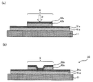
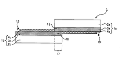
- FIG. 1A embodiment and 1B embodiment show an electroconductive base material. It is process drawing which shows an example of the manufacturing method of the electroconductive base material using the laminated body of the 1B embodiment. It is process drawing which shows the other example of the manufacturing method of the electroconductive base material using the laminated body of the 1B embodiment. It is process drawing which shows the other example of the manufacturing method of the electroconductive base material using the laminated body of the 1B embodiment. It is process drawing which shows the other example of the manufacturing method of the electroconductive base material using the laminated body of the 1B embodiment. It is a schematic plan view which shows an example of the laminated body of a 2nd embodiment. FIG. 3 is a sectional view taken along line AA in FIG. 2. It is a schematic sectional drawing which shows the other example of the laminated body of a 2nd embodiment.
- the laminate of the present disclosure the method for producing a conductive substrate using the laminate, the method for producing an electronic device, and the transfer tool will be described in detail.
- Laminate The laminate of the present disclosure is opposite to the first substrate, the first porous conductive layer on one side of the first substrate, and the first substrate of the first porous conductive layer.
- This is a member having a first conductive substrate laminated with a first adhesive layer on the side surface.
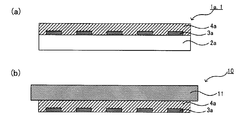
- FIG. 1 is a schematic cross-sectional view illustrating an example of a laminate according to one embodiment of the present disclosure.
- the laminate 1 includes a first base material 2a, a first porous conductive layer 3a on one surface of the first base material 2a, and a first base material of the porous conductive layer 3a. It has a first conductive substrate 1a having a first adhesive layer 4a on the surface opposite to 2a.
- this embodiment is referred to as a first embodiment.
- the laminate in one embodiment of the present disclosure will be described separately for the first embodiment, the second embodiment, and the third embodiment.
- a laminate of the first embodiment includes a first base material, a first porous conductive layer on one surface of the first base material, and the first group of the first porous conductive layer.
- the first adhesive layer in the laminate of the first embodiment is formed on the first porous conductive layer, and the first porous layer is transferred when the laminate of the first embodiment is transferred to the transfer substrate.
- the conductive conductive layer and the substrate to be transferred are not particularly limited as long as they have a function of adhering.
- the first adhesive layer in the first embodiment may be a pressure-sensitive adhesive layer or may not be a pressure-sensitive adhesive layer.
- an embodiment in which the first adhesive layer is not a pressure-sensitive adhesive layer will be described as a 1A embodiment, and an embodiment in which the first adhesive layer is a pressure-sensitive adhesive layer will be described separately as a 1B embodiment.
- the laminate of the 1A embodiment includes a first substrate, a first porous conductive layer on one surface of the first substrate, and the first group of the first porous conductive layer.
- FIG. 1 is a schematic cross-sectional view showing an example of the laminate of the first embodiment. Note that the description of FIG. 1 can be the same as that described above, and thus the description thereof is omitted here.
- FIG. 2A to 2 (c) are process diagrams showing an example of a method for producing a conductive base material using the laminate of the embodiment 1A, and an example using the laminate shown in FIG. .
- the laminate 1 and the substrate to be transferred 11 are prepared.
- the first adhesive layer 4a of the laminated body 1 and the transferred substrate 11 are arranged so as to contact each other, and thermocompression bonding is performed from the laminated body 1 side.
- the 1st base material 2a is peeled.
- the 1st contact bonding layer 4a and the 1st porous conductive layer 3a are transcribe
- 3 (a) to 3 (c) are process diagrams showing another example of a method for producing a conductive base material using the laminate of the embodiment 1A, and an example using the laminate shown in FIG. It is.
- the laminate 1 and the substrate to be transferred 11 are prepared.
- the first adhesive layer 4a of the laminate 1 and the transferred substrate 11 are arranged so as to be in contact with each other, and thermocompression bonding is performed from the laminate 1 side.
- partial thermal compression bonding is performed by the thermal head 12 of the thermal head printer.
- the 1st base material 2a side is peeled.
- the first adhesive layer 4a and the first porous conductive layer 3a are transferred to the substrate 11 to be transferred, and the conductive having the pattern of the first adhesive layer 4a and the first porous conductive layer 3a.
- the base material 10 is obtained.
- the component derived from the first adhesive layer for example, the resin contained in the first adhesive layer
- the component derived from the first adhesive layer can be introduced into the pores of the first porous conductive layer.
- thermal diffusion can be made difficult to occur. Therefore, when transferring the laminate of the first embodiment to the transfer substrate, it is difficult for heat to escape, so there is no need to heat excessively, which is advantageous for thermal transfer.
- the component derived from the first adhesive layer can be introduced into the pores of the first porous conductive layer, the first porous conductive layer and the first adhesive layer In addition to increasing the surface area in contact with each other, the anchoring effect can enhance the adhesion between the first porous conductive layer and the first adhesive layer. Therefore, when transferring the laminate of the embodiment 1A to the substrate to be transferred, the first adhesive layer and the first porous conductive layer can be satisfactorily transferred to the substrate to be transferred, and excellent transferability is achieved. Can be obtained.
- metal particles may be sintered and fused, so that the first porous conductive layer is derived from the first adhesive layer inside the pores of the first porous conductive layer.
- the region where the component enters also contributes to the conductivity. Therefore, the adhesiveness with the first adhesive layer can be improved without reducing the conductivity.
- the conductivity of conductive materials such as metals and metal oxides may decrease due to oxidation, and the first porosity is used when the laminate of the first embodiment is transferred to the substrate to be transferred. There is a possibility that the conductivity of the conductive layer is lowered.
- the laminate of the 1A embodiment since the resin contained in the first adhesive layer can enter the pores of the first porous conductive layer, the laminate of the 1A embodiment When transferring to the substrate to be transferred, the first porous conductive layer can be protected with the resin contained in the first adhesive layer, and oxidation of the first porous conductive layer can be suppressed. Therefore, it is possible to suppress a decrease in conductivity of the first porous conductive layer during transfer.
- the first porous conductive layer is porous, brittleness is imparted. Therefore, unlike the conventional deposited layer, the generation of burrs during transfer is small and large crystal grains are included. There is nothing. Therefore, good foil breakability can be obtained. Further, as illustrated in FIGS. 3A to 3C, when the patterns of the first adhesive layer and the first porous conductive layer of the laminate of the first embodiment are transferred to a substrate to be transferred. Can be transferred with good resolution.
- metal particles are sintered at a low temperature when the particle size is reduced.
- the metal particles are sintered at a low temperature by utilizing the property that when such metal particles are converted into nanoparticles, the metal particles are sintered at a temperature much lower than the melting point of the metal particles.
- a conductive conductive layer can be formed. Therefore, there is little damage to the substrate, and it is not necessary to use a substrate having high heat resistance, and a substrate having low heat resistance can also be used.
- an inexpensive general-purpose plastic resin substrate such as polyethylene terephthalate can be used.
- the first porous conductive layer can be formed by, for example, applying a metal particle dispersion containing metal particles on the first base material and firing the first base base material.
- a first porous conductive layer having good adhesion can be obtained. Therefore, it is not necessary to form another layer on the base material or to perform surface treatment in order to improve adhesion.
- the 1st porous conductive layer can be formed on a to-be-transferred base material by transcribe
- a substrate that has been difficult to form a porous conductive layer can also be used. Therefore, an inexpensive general-purpose plastic resin base material such as polyethylene terephthalate or a conductive base material in which the first porous conductive layer is formed on a paper base material can be obtained. Furthermore, it is possible to form the first porous conductive layer on the substrate to be transferred which is a three-dimensional object.
- the 1st conductive substrate in 1A embodiment is the 1st base material, the 1st porous conductive layer on one side of the 1st base material, and the 1st porous conductive layer first 1 is a member in which a first adhesive layer on a surface opposite to a base material is laminated.
- (A) 1st porous conductive layer The 1st porous conductive layer in the 1A embodiment is formed on the 1st substrate.
- the first porous conductive layer refers to a conductive layer having a plurality of holes, and the surface area is larger than that of a conductive layer having the same volume and having no holes.
- Examples of the conductive material constituting the first porous conductive layer include metals and metal oxides.
- the conductive material constituting the first porous conductive layer may be one type or two or more types. Of these, metals are preferred. This is because the metal particles can be sintered at a lower temperature to form the first porous conductive layer.
- the metal examples include gold, silver, copper, nickel, platinum, palladium, molybdenum, aluminum, antimony, tin, chromium, indium, gallium, germanium, zinc, titanium, lead, and the like.
- silver and copper are preferable from the viewpoint of conductivity and cost.
- 1 type may be sufficient as a metal and 2 or more types may be sufficient as it.
- the metal oxide include indium tin oxide and antimony-doped tin oxide.
- the shape of the holes in the first porous conductive layer is preferably not particularly limited, and is preferably a shape in which a component derived from the first adhesive layer can enter at least some of the holes. It is preferable that at least the surface on the first adhesive layer side of the first porous conductive layer has a communication hole in which a plurality of holes are connected to each other.
- the porosity of the first porous conductive layer is not particularly limited as long as the conductivity and adhesion can be adjusted as appropriate. Specifically, the porosity of the first porous conductive layer is preferably 5% or more, more preferably 10% or more, and particularly preferably 15% or more. Further, the porosity of the first porous conductive layer is preferably 50% or less, more preferably 45% or less, and particularly preferably 40% or less. When the porosity has the above upper limit, it is possible to suppress a decrease in adhesion between the first porous conductive layer and the first substrate. Moreover, when the porosity has the above lower limit, the above-described effect due to the component derived from the first adhesive layer entering the pores of the first porous conductive layer can be sufficiently obtained.
- the porosity of the first porous conductive layer represents a portion where the material constituting the first porous conductive layer does not exist, and the portion where the components derived from the first adhesive layer are mixed included.
- the porosity can be confirmed from a scanning electron microscope (SEM) image of the cross section of the first porous conductive layer before forming the first adhesive layer. Specifically, the area of the pores and the area of the first porous conductive layer are calculated from the obtained SEM image, and the area of the pores is divided by the area of the first porous conductive layer, whereby the voids in the cross section are calculated.
- the porosity can be determined. The porosity is calculated from the first porous conductive layer excluding the base material, and pores at the interface between the base material, the first porous conductive layer, and the interface are included in the first porous conductive layer. The porosity can also be confirmed from a scanning electron microscope (SEM) image of the cross section of the laminate.
- SEM scanning electron microscope
- the area of the hole, the area of the component derived from the first adhesive layer, and the area of the first porous conductive layer are calculated from the obtained SEM image, respectively, and the area of the hole and the first adhesive layer are derived.
- the porosity in the cross section can be obtained by dividing the total of the components by the area of the first porous conductive layer.
- the numerical range mentioned above points out the average value calculated
- the porosity is similarly determined for a plurality of cross sections as appropriate according to the size of the laminate, and the average value is taken as the porosity of the first porous conductive layer.
- the porosity can be appropriately adjusted according to the particle diameter of the metal particles used in the metal particle dispersion, the type of the dispersant, the firing conditions, and the like in the first porous conductive layer forming method described later.
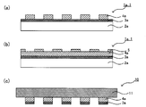
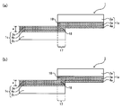
- the first porous conductive layer 3a may be formed on the entire surface of the first substrate 2a as illustrated in FIG. 1, and the pattern is formed on the first substrate 2a as illustrated in FIG. 4 (a). It may be formed in a shape. As shown in FIG. 4A, when the first porous conductive layer 3a is formed in a pattern on the first substrate 2a, the layered body 1 is not partially transferred, but FIG. As shown in b), the pattern of the first porous conductive layer 3a can be transferred onto the substrate 11 to be transferred.
- the thickness of the first porous conductive layer is about 0.01 ⁇ m or more, preferably 0.05 ⁇ m or more, particularly preferably 0.1 ⁇ m or more.
- the thickness of the first porous conductive layer is about 50 ⁇ m or less, preferably 10 ⁇ m or less, particularly preferably 5 ⁇ m or less.
- the first porous conductive layer As a method for forming the first porous conductive layer, there is used a method in which a metal particle dispersion containing metal particles is applied onto a first substrate and fired.
- the metal particles include alloy particles, metal compound particles, and the like in addition to metal particles.
- the metal particles can be appropriately selected from metal particles that produce conductivity after firing.
- the metal constituting the metal particles include gold, silver, copper, nickel, platinum, palladium, molybdenum, aluminum, antimony, tin, chromium, indium, gallium, germanium, zinc, titanium, lead, and the like. Among these, silver and copper are preferable from the viewpoint of conductivity and cost.
- the metal constituting the metal particles may be one kind or two or more kinds. Further, a metal in which two or more kinds of metals form a core-shell structure, a metal in which the surface of particles in a metal state is oxidized or nitrided, or the like may be used. The surface of the metal particles may be oxidized or may be oxidized to the inside.
- the metal compound constituting the metal compound particles include metal oxides, metal nitrides, metal hydrides, metal hydroxides, and organometallic compounds. These metal compounds are preferably those which are decomposed into a metal state upon firing. For example, particles of a metal compound that exhibits conductivity by reduction, specifically, particles of a metal compound such as cuprous oxide, cupric oxide, silver oxide, copper nitride, copper hydride, and the like can be given. Examples of the metal oxide include indium tin oxide and antimony-doped tin oxide. A metal particle may be used individually by 1 type and may be used in combination of 2 or more type. Among these, particles in a metal state are preferable. This is because the metal particles can be sintered at a lower temperature to form the first porous conductive layer.
- the metal particles are preferably metal nanoparticles. That is, the first porous conductive layer is preferably a sintered body of metal nanoparticles.
- the pore diameter and crystal grain size can be controlled within a range suitable for foil breakability. It is.
- the average particle size of the metal particles is preferably 1 nm or more, and more preferably 2 nm or more. Further, the average particle diameter of the metal particles is preferably 200 nm or less, more preferably 150 nm or less, and particularly preferably 100 nm or less. When the average particle size is within the above range, the dispersion stability of the metal particle dispersion used for forming the first porous conductive layer is good, and the conductivity when the first porous conductive layer is formed. The melting point is kept low, sufficient sintering is possible, and high conductivity is obtained.
- the average particle diameter of the metal particles is the average primary particle diameter of the metal particles in the metal particle dispersion, and can be measured from an observation image obtained by a transmission electron microscope. Moreover, the numerical range mentioned above points out the average value calculated
- a method for preparing metal particles for example, a physical method obtained by pulverizing metal powder or metal oxide powder by a mechanochemical method or the like; CVD method, vapor deposition method, sputtering method, thermal plasma method, laser method, etc.
- a chemical dry method a method called a chemical wet method using a thermal decomposition method, a chemical reduction method, an electrolysis method, an ultrasonic method, a laser ablation method, a supercritical fluid method, a microwave synthesis method, or the like can be given.
- the obtained metal particles are obtained by using a protective agent such as a water-soluble polymer compound such as polyvinylpyrrolidone or a graft copolymer polymer compound, a surfactant, a metal or a metal oxide. It is preferable to coat with a compound having a thiol group, amino group, hydroxyl group, or carboxyl group that interacts with the product. Depending on the method of synthesizing the metal particles, the pyrolyzate or oxide of the raw material may protect the particle surface and contribute to dispersibility.
- a protective agent such as a water-soluble polymer compound such as polyvinylpyrrolidone or a graft copolymer polymer compound, a surfactant, a metal or a metal oxide. It is preferable to coat with a compound having a thiol group, amino group, hydroxyl group, or carboxyl group that interacts with the product.
- the pyrolyzate or oxide of the raw material may protect the particle
- the reducing agent or the like may act as a protective agent for the metal particles as it is.
- surface treatment of the metal particles is performed, or a dispersant composed of a polymer compound, an ionic compound, a surfactant or the like is added to the metal particle dispersion liquid. May be.
- the dispersion medium used in the metal particle dispersion is preferably one that can disperse metal particles.
- water or an organic solvent can be used.
- the organic solvent include alcohols, ketones, esters, ethers, aliphatic hydrocarbons, alicyclic hydrocarbons, aromatic hydrocarbons, and the like.
- a viscosity modifier such as a viscosity modifier, a surface tension modifier, a stabilizer, or the like may be added to the metal particle dispersion as necessary.
- the metal particle dispersion preferably has a solid content concentration of 5% by mass or more, more preferably 10% by mass or more, and particularly preferably 15% by mass or more.
- the metal particle dispersion preferably has a solid content concentration of 95% by mass or less, more preferably 90% by mass or less, and particularly preferably 85% by mass or less. When the solid content concentration is within the above range, sufficient conductivity is obtained, the viscosity is sufficiently low, and the metal particle dispersion can be easily applied to the substrate.
- the metal particle dispersion When applying the metal particle dispersion on the first substrate, the metal particle dispersion may be applied to the entire surface of the first substrate, and the metal particle dispersion in a pattern on the first substrate. It may be applied.
- the method for applying the metal particle dispersion on the first substrate include gravure printing, screen printing, spray coating, spin coating, comma coating, bar coating, knife coating, die coating, offset printing, flexographic printing, and inkjet printing. And dispenser printing. In the case where the metal particle dispersion is applied in a pattern on the first substrate, gravure printing, flexographic printing, screen printing, and inkjet printing are preferable from the viewpoint that fine patterning can be performed.
- drying may be performed by a normal method.
- the drying method which heats for about 0.1 minutes or more and 20 minutes or less at the temperature of about 80 degreeC or more and 140 degrees C or less using a general oven etc. is mentioned.
- the thickness of the coating film after drying can be controlled by adjusting the coating amount, the average particle diameter of the metal particles, and the like, it is usually about 0.01 ⁇ m or more, preferably 0.1 ⁇ m or more.
- the thickness of the coating film after drying is about 100 ⁇ m or less, preferably 50 ⁇ m or less.
- the method for firing the coating film of the metal particle dispersion may be any method that can sinter the metal particles, and a general firing method can be applied.
- a heat treatment method, a light treatment method, a plasma treatment method, or the like can be given.
- a first porous conductive layer made of a sintered body of metal particles is obtained.
- the heat treatment include hot plate heating, hot air heating, hot pressing using a hot plate or a hot roll.
- the light treatment include laser treatment, ultraviolet lamp treatment, infrared lamp treatment, far-infrared lamp treatment, and flash light lamp treatment.
- the plasma treatment is a treatment that ionizes gases such as hydrogen, carbon monoxide, ammonia, alcohol, etc.
- ECR electron cyclotron resonance
- Capacitively coupled plasma, inductively coupled plasma, atmospheric pressure plasma, microwave plasma, surface wave plasma generated by application of microwave energy, and the like is preferable.
- surface wave plasma treatment is preferable.
- said baking method can be used in combination of 2 or more type.
- Microwave surface wave plasma has the characteristics of high plasma density and low electron temperature, and the coating film can be fired at low temperature in a short time, forming a dense and smooth first porous conductive layer can do.
- the surface wave plasma is irradiated with plasma having a uniform density within the surface with respect to the processing surface.
- it is less likely to form a non-uniform film such as partial sintering of metal particles in the plane, and grain growth can be prevented.
- a dense and smooth film can be obtained.
- contamination of impurities derived from the electrode can be prevented, and damage to the processing material due to abnormal discharge can be prevented.
- a resin base material there is little damage to a resin base material, and there is also little damage to another layer.
- the microwave surface wave plasma is suitable for improving the adhesion of the first porous conductive layer to the resin base material. This is presumably because the microwave surface wave plasma is likely to generate a polar functional group such as a hydroxyl group or a carboxyl group at the interface between the first base material and the first porous conductive layer.
- a plasma generated in a reducing gas atmosphere is used for a polyester substrate, the plasma of the gas having a reducing gas reacts with the ester bond of the first substrate, It is presumed that the adhesion at the interface between the first porous conductive layer and the first base material is improved because modification occurs on the interface side and many reactive groups with high polarity are generated.
- the microwave surface wave plasma can be compared with the conventional method in which the surface of the substrate is previously roughened by plasma treatment or the like to improve the adhesion with the first porous conductive layer. It is excellent in that the adhesion between the first porous conductive layer and the first porous conductive layer is high.
- the atmosphere at the time of firing is appropriately selected according to the type of conductive material constituting the first porous conductive layer.
- the first porous conductive layer containing metal it is preferable to use an atmosphere of an inert gas or a reducing gas, and it is particularly preferable to use a reducing gas.
- a reducing gas atmosphere the oxide present on the surface of the metal particles is reduced and removed, and the first porous conductive layer having good conductivity can be formed. Therefore, when forming the 1st porous conductive layer containing a metal, the metal particle by which the surface was oxidized and the metal particle by which the inside was oxidized can be used as a metal particle.
- the reducing gas examples include hydrogen, carbon monoxide, ammonia, and a mixed gas thereof. Of these, hydrogen gas is preferred. Hydrogen gas is suitable for removing organic substances adhering to the surface of the metal particles.
- the reducing gas may be mixed with an inert gas such as nitrogen, helium, argon, neon, krypton, or xenon. In this case, there is an effect that plasma is easily generated.
- the atmosphere may contain an inert gas such as nitrogen or argon and, if necessary, oxygen.
- the method by hydrogen plasma or nitrogen plasma is preferable.
- a specific resistance of about 3 ⁇ 10 ⁇ 6 ⁇ ⁇ cm to 3 ⁇ 10 ⁇ 5 ⁇ ⁇ cm can be obtained, and the first porosity has good adhesion to the first substrate. This is because a conductive layer can be formed.
- the firing temperature may be any temperature at which the metal particles can be sintered, and is appropriately selected according to the type, particle diameter, firing method, and the like of the metal particles. Especially, it is preferable that a calcination temperature is below the heat-resistant temperature of a 1st base material, and the inside of the range of 100 degreeC or more and 150 degrees C or less is preferable if silver particle is made into an example.
- the firing time is appropriately selected according to the type of metal particles, the firing method, and the like. For example, when silver particles are baked by heat treatment, the baking time is preferably 10 minutes or longer, more preferably 15 minutes or longer, and preferably 120 minutes or shorter, especially 40 minutes or shorter. It is preferable. For example, when copper particles are fired by hydrogen plasma, the firing time is preferably 1 minute or more, more preferably 2 minutes or more, and preferably 10 minutes or less, especially 5 minutes or less. It is preferable that
- the 1st adhesion layer in the 1A embodiment is formed on the 1st above-mentioned porous conductive layer.
- the first adhesive layer has a function of adhering the first porous conductive layer and the transferred substrate when transferring the laminate of the 1A embodiment to the transferred substrate.
- Examples of the material for the first adhesive layer include thermoplastic resins and photosensitive resins whose adhesiveness or adhesiveness is reduced by light irradiation.
- the thermoplastic resin is preferably one that can adhere the first porous conductive layer and the substrate to be transferred, and is appropriately selected according to the type of the substrate to which the laminate is transferred.
- a general thermoplastic resin used for the transfer foil can be used.
- the thermoplastic resin is preferably one that is heated, melted or softened to develop tackiness or adhesiveness, and a curable resin that is partially cured may be used.
- Conventional adhesives such as urethane resins, ionomer resins, vinyl chloride resins, vinyl acetate resins, vinyl chloride-vinyl acetate copolymer resins, polyester resins and polyamide resins can be widely used.
- a thermoplastic resin may be used individually by 1 type, and may be used in combination of 2 or more type.
- the photosensitive resin whose tackiness or adhesiveness is reduced by light irradiation for example, it is cured by irradiation with light of a specific wavelength such as ultraviolet ray, visible light, infrared ray, etc., and the tackiness or adhesiveness is lowered, and In the non-light-irradiated portion, a material capable of bonding the first porous conductive layer and the substrate to be transferred can be used.
- known materials such as polyfunctional (meth) acrylic resins formulated with photopolymerization initiators or photocurable varnishes formulated with epoxy resins with photoacid generators or photobase generators are widely used. it can.
- a solvent dilution type a W / O emulsion type, or a non-sol type that does not contain a solvent may be used.
- Such photosensitive resin may be used individually by 1 type, and may be used in combination of 2 or more type.
- the first adhesive layer may contain an additive in addition to the thermoplastic resin or the photosensitive resin.
- the additive include a dispersant, a filler, a plasticizer, and an antistatic agent.
- the first adhesive layer 4 may be formed on the entire surface of the first base material 2a as illustrated in FIG. 1, and the first group as illustrated in FIG. 5A. It may be formed in a pattern on the material 2a.
- the first adhesive layer 4a is formed in a pattern on the first substrate 2a as shown in FIG. 5 (a), even if the laminate 1 is not partially transferred, FIG. 5 (c)
- the pattern of the 1st porous conductive layer 3a can be transcribe
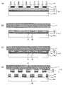
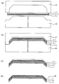
- the 6 (a) to 6 (d) are process diagrams showing another example of a method for producing a conductive base material using the laminate of the 1A embodiment, and the first adhesive layer 4a is adhered by light irradiation. This is an example in which a photosensitive resin whose property or adhesiveness is lowered is used.
- stacked in order on the 1st base material 2a was prepared, and the 1st contact bonding layer 4a
- the light 16 is irradiated in a pattern through the photomask 15 to reduce the adhesiveness or adhesiveness in the light irradiation portion of the first adhesive layer 4a, and the low adhesion portion 42 is formed.
- the first adhesive layer 4a of the laminated body 1 and the transferred substrate 11 are arranged so as to be in contact with each other, and are brought into close contact with each other. Thereafter, as shown in FIG.
- the first substrate 2a side is peeled off. Since the first adhesive layer 4a has an adhesive portion 41 that is a non-light-irradiated portion and a low-adhesion portion 42 that is a light-irradiated portion and has reduced adhesiveness or adhesiveness, However, in the low adhesion part 42, the adhesion to the substrate 11 to be transferred is lowered. Therefore, when the first base material 2a side is peeled off, the first porous conductive layer 3a and the first adhesive layer 4a are peeled off together with the first base material 2a in the low adhesion portion 42, and the transferred base material in the adhesion portion 41 11, the first porous conductive layer 3a is transferred.
- the electroconductive base material 10 which has the pattern of the 1st contact bonding layer 4a and the 1st porous conductive layer 3a is obtained. Also in this case, the pattern of the first porous conductive layer 3a can be transferred onto the substrate 11 to be transferred without partially transferring the laminate 1.
- the thickness of the first adhesive layer is preferably such a thickness that the foil can be cut when the laminate of the first embodiment is transferred to the transfer substrate, depending on the transfer method, the type of transfer substrate, and the like. It is selected appropriately. Specifically, the thickness of the first adhesive layer is preferably 0.1 ⁇ m or more, and more preferably 1 ⁇ m or more. Further, the thickness of the first adhesive layer is preferably 50 ⁇ m or less, and more preferably 25 ⁇ m or less. When the thickness of the first adhesive layer has the above lower limit, it is possible to sufficiently secure the adhesiveness to the transfer substrate.
- the thickness of the first adhesive layer has the above upper limit, the temperature for heating the first adhesive layer becomes too high when transferring the laminate of the first A embodiment, and the transfer target substrate or the like becomes Problems such as damage can be suppressed.
- the substrate to be transferred is a paper substrate, some paper substrates are difficult to transfer depending on the type.
- the thickness of the first adhesive layer is in the above range. Of these, a relatively thick film is preferable.
- the thickness of the first adhesive layer is relatively thick within the above range.
- Examples of the method for forming the first adhesive layer include a method in which a resin composition is applied on the first porous conductive layer and dried.
- a coating method of the resin composition it can be applied by appropriately selecting from general coating methods.
- the non-first adhesive layer 5 may be formed in a pattern on the first adhesive layer 4a. Also in this case, the pattern of the first porous conductive layer 3a can be transferred onto the transfer substrate 11 as shown in FIG.
- the material of the non-first adhesive layer examples include a thermoplastic resin that does not melt at a temperature at which the first adhesive layer melts, a thermosetting resin, and a photocurable resin.
- the thickness of the non-first adhesive layer is preferably a thickness that allows the first adhesive layer and the transferred substrate to be bonded when transferring the laminate of the present disclosure to the transferred substrate. It is appropriately selected depending on the transfer method, the type of substrate to be transferred and the like. Specifically, the thickness of the non-first adhesive layer is preferably 100 nm or more and 3 ⁇ m or less.
- the method for forming the non-first adhesive layer include a method in which the resin composition is applied in a pattern on the first adhesive layer, dried, and cured as necessary. As a coating method of the resin composition, it can be applied by appropriately selecting from general coating methods.
- the 1st base material in 1A embodiment supports said 1st porous conductive layer and 1st contact bonding layer.
- the first substrate is not particularly limited as long as the first porous conductive layer can be formed.
- an inorganic substrate such as a glass substrate or a ceramic substrate, a metal substrate, or a resin substrate.
- a paper base material or the like can be used.
- a 1st base material is a resin base material.
- the first porous conductive layer can be formed by sintering the metal particles at a low temperature, the first base material is hardly damaged and a base material having high heat resistance is used. There is no need, and a substrate having low heat resistance can also be used.
- an inexpensive general-purpose plastic resin substrate such as polyethylene terephthalate can be used.
- a general resin substrate can be used as the resin substrate.
- Preferred examples of the resin substrate include polyimide, polyamide, polyamideimide, polyethylene terephthalate, polyethylene naphthalate, polyphenylene sulfide, polyether ether ketone, polyether sulfone, polycarbonate, polyether imide, epoxy resin, phenol resin, and glass.
- -Resin films such as epoxy resins, polyphenylene ethers, acrylic resins, polyolefins such as polyethylene and polypropylene, polycycloolefins such as polynorbornene, and liquid crystalline polymer compounds.
- an inexpensive general-purpose plastic resin base material such as polyethylene terephthalate is preferable.
- the first base material may have flexibility or rigidity, and is appropriately selected according to a method for transferring the laminate of the 1A embodiment to the transfer target substrate. Especially, it is preferable that a 1st base material has flexibility, and it is more preferable that it is a resin base material which has flexibility from the reason mentioned above.
- a release layer may be formed on the surface of the first base material, or a release treatment may be performed. This is because peeling between the first substrate and the first porous conductive layer or the first protective layer is facilitated.
- the material for the release layer include a fluorine release agent, a silicone release agent, and a wax release agent.
- the method for forming the release layer include a method in which a release agent is applied by a coating method such as dip coating, spray coating, or roll coating.
- the mold release treatment include surface treatment such as fluorine treatment and silicone treatment.
- the thickness of the first base material is not particularly limited, but in the case of an inorganic base material, it is usually 0.1 mm or more, preferably 0.5 mm or more, and usually 10 mm or less. , Preferably 5 mm or less.
- the thickness of the base material is usually 1.0 ⁇ m or more and 1000 ⁇ m or less.
- the laminated body of the 1A embodiment may have other configurations as necessary in addition to the first base material, the first porous conductive layer, and the first adhesive layer.
- an antistatic layer, a heat-resistant first protective layer, a rub-resistant layer, a slipping layer, and the like may be provided on the surface of the first substrate opposite to the surface on which the first porous conductive layer is formed.
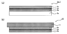
- the 1st protective layer may be formed between the 1st base material and the 1st porous conductive layer.
- the first protective layer will be described.
- a first protective layer 6a may be formed between the first substrate 2a and the first porous conductive layer 3a.
- the first protective layer 6 a is a conductive first base material after the first porous conductive layer 3 a is transferred from the laminate 1 to the transferred first base material 11. Therefore, the first porous conductive layer 3a can be protected from abrasion, light, chemicals, and the like.
- a 1st porous conductive layer can be insulated by setting it as the 1st protective layer which has insulation.
- the first porous conductive layer can be protected and preferably has an insulating property, and examples thereof include an ultraviolet curable resin and an electron beam curable resin.
- the first protective layer may further contain a filler.
- Examples of the method for forming the first protective layer include a method in which a curable resin composition is applied on a first substrate and dried.
- Examples of the method for applying the curable resin composition include a gravure coating method, a roll coating method, a comma coating method, a gravure printing method, a screen printing method, and a gravure reverse roll coating method.
- a protective film as a 1st protective layer, a 1st base material and a protective film can be bonded together via a weak adhesion layer. It is preferable that the weak adhesive layer is capable of peeling the weak adhesive layer together with the first base material when the first base material is peeled off.
- the thickness of the first protective layer is preferably 0.5 ⁇ m or more, and more preferably 3 ⁇ m or more. Moreover, it is preferable that the thickness of a 1st protective layer is 30 micrometers or less, and it is preferable that it is 15 micrometers or less especially. When the thickness of the first protective layer is within the above range, surface properties such as excellent high hardness, scratch resistance, chemical resistance and stain resistance can be obtained, and further excellent moldability and shape followability can be obtained. be able to.
- the laminate of the 1A embodiment can be used for the production of a conductive substrate as will be described later.
- a printed wiring board, an electromagnetic wave shielding material, an antenna, a power semiconductor, a noise filter, a capacitor electrode, Various sensor electrodes (touch sensors, biosensors, temperature sensors, gas sensors, optical sensors, pressure sensors, flow sensors), display electrodes, solar cell electrodes, IC cards, RFID, etc., and bonding materials, connector materials can be used.
- the laminate of the first embodiment can be used as an electromagnetic wave shielding layer for preventing unauthorized reading of information recorded on the non-contact type IC card and a conductive layer for modulating the resonance frequency.
- the first porous conductive layer can be applied to a part of the card and transported in a state where reading is impossible, and the first adhesive layer can be scratched and removed at the time of use. Since the laminated body of the 1A embodiment has the first porous conductive layer, it can be easily peeled by scratch by controlling the adhesive force of the first adhesive layer. In addition, the laminate of the 1A embodiment can also be used to form designs, designs, characters, and the like that make use of the color and gloss of the first porous conductive layer.
- the laminate of the 1B embodiment includes a first substrate, a first porous conductive layer on one surface of the first substrate, and the first group of the first porous conductive layer. It is a member having a first conductive substrate in which a first adhesive layer on a surface opposite to the material is laminated, and the first adhesive layer is a pressure-sensitive adhesive layer.
- FIG. 1 is a schematic cross-sectional view showing an example of the laminate of the first embodiment. Note that the description of FIG. 1 can be the same as that described above, and thus the description thereof is omitted here.
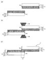
- FIG. 8A to 8 (c) are process diagrams showing an example of a method for producing a conductive base material using the laminate of the 1B embodiment, and an example using the laminate exemplified in FIG. is there.
- the laminate 1 and the substrate to be transferred 11 are prepared.
- the pressure-sensitive adhesive layer 4 a of the laminate 1 is arranged so as to be in contact with the transferred substrate 11, and the laminate 1 is pressed from the laminate 1 side.
- the 1st base material 2a is peeled.
- the pressure-sensitive adhesive layer 4a and the first porous conductive layer 3a are transferred to the transfer target substrate 11 in the pressed region, and the conductive substrate 10 is obtained.
- FIG. 9 (a) to 9 (c) are process diagrams showing another example of a method for producing a conductive substrate using the laminate of the 1B embodiment, and an example using the laminate shown in FIG. It is.
- the laminate 1 and the substrate to be transferred 11 are prepared.
- the pressure-sensitive adhesive layer 4 a of the laminate 1 is disposed so as to be in contact with the transferred substrate 11, and the laminate 1 is pressure-bonded from the laminate 1 side. At this time, partial pressing is performed with the uneven plate 12 or the like.
- FIG.9 (c) the 1st base material 2a side is peeled.
- the pressure-sensitive adhesive layer 4a and the first porous conductive layer 3a are transferred to the transfer substrate 11 in the pressure-bonded region, and the conductive material having the pattern of the pressure-sensitive adhesive layer 4a and the first porous conductive layer 3a.
- the base material 10 is obtained.
- FIGS. 10A and 10B are process diagrams showing another example of a method for producing a conductive base material using the laminate of the 1B embodiment.
- FIG. 10A and FIG. 10B are examples using a transfer tool having a strip-shaped laminate.
- FIG. 10B is a schematic plan view of the portion A of FIG. 10A viewed from the first porous conductive layer 3a side.
- a strip-shaped laminate 1 and a substrate to be transferred 11 are prepared.
- the transfer tool 20 is used so that the pressure-sensitive adhesive layer 4a of the laminate 1 and the substrate 11 to be transferred are in contact with each other, and the transfer tool 20 is moved in a predetermined direction while applying pressure from the laminate 1 side. To do.
- the pressure-sensitive adhesive layer 4a and the first porous conductive layer 3a are transferred onto the transfer substrate 11 along the moving direction of the transfer tool 20, and the first substrate 2a is peeled off.
- the patterns of the pressure-sensitive adhesive layer 4a and the first porous conductive layer 3a can be transferred onto the transfer substrate 11 as shown in FIGS. 10 (a) and 10 (b).
- the transfer tool 20 will be described later.
- the resin contained in the pressure-sensitive adhesive layer can be introduced into the pores of the first porous conductive layer, the surface area to which the first porous conductive layer and the pressure-sensitive adhesive layer adhere is reduced. Not only becomes large, but also the adhesion between the first porous conductive layer and the pressure-sensitive adhesive layer can be enhanced by the anchor effect. Therefore, when transferring the laminate of the first embodiment to the transfer substrate, the pressure-sensitive adhesive layer and the first porous conductive layer can be satisfactorily transferred to the transfer substrate, and excellent transferability is achieved. Can be obtained.
- metal particles may be sintered and fused, so that the first porous conductive layer is derived from the first adhesive layer inside the pores of the first porous conductive layer.
- the region where the component enters also contributes to the conductivity. Therefore, the adhesiveness with the first adhesive layer can be improved without reducing the conductivity.
- a pressure-sensitive adhesive can be used as the pressure-sensitive adhesive layer, heating is not required when transferring the laminate onto the substrate to be transferred. It is possible to suppress a decrease in conductivity due to oxidation of the conductive layer, distortion of the stacked body, and the like.
- the first porous conductive layer is porous, brittleness is imparted, and unlike the conventional vapor deposition layer, the generation of burrs is small during transfer, and large crystal grains are included. There is nothing. Therefore, good foil breakability can be obtained. Further, as illustrated in FIGS. 9A to 9C, when the pattern of the pressure-sensitive adhesive layer and the first porous conductive layer of the laminate of the 1B embodiment is transferred to a substrate to be transferred. Can be transferred with good resolution.
- metal particles are sintered at a low temperature when the particle size is reduced.
- the metal particles are sintered at a low temperature by utilizing the property that such metal particles are sintered at a temperature much lower than the melting point of the metal particles.
- a conductive conductive layer can be formed. Therefore, there is little damage to the first substrate, it is not necessary to use a substrate having high heat resistance, and a substrate having low heat resistance can also be used.
- an inexpensive general-purpose plastic resin substrate such as polyethylene terephthalate can be used.
- the first porous conductive layer can be formed, for example, by applying a metal particle dispersion containing metal particles on the first base material and firing the first base base material.
- a first porous conductive layer having good adhesion can be obtained. Therefore, it is not necessary to form another layer or perform a surface treatment on the first base material in order to improve adhesion.
- the 1st porous conductive layer can be formed on a to-be-transferred base material by transcribe
- the 1st base material in which it was difficult to form a porous conductive layer can also be used. Therefore, an inexpensive general-purpose plastic resin base material such as polyethylene terephthalate or a conductive base material in which the first porous conductive layer is formed on a paper base material can be obtained. Furthermore, it is possible to form the first porous conductive layer on the substrate to be transferred which is a three-dimensional object.
- the first porous conductive layer in the 1B embodiment is porous, it can exhibit high resistance to bending. Therefore, when the first substrate has flexibility, it can be transferred to the substrate to be transferred while giving the laminate a high curvature.
- the 1st conductive substrate in the 1B embodiment is the 1st base material, the 1st porous conductive layer on one side of the 1st base material, and the 1st porous conductive layer first 1 is a member in which a first adhesive layer on the surface opposite to the substrate is laminated, and the first adhesive layer is a pressure-sensitive adhesive layer.
- the first porous conductive layer in the 1B embodiment is formed on the first base material.
- the 1st porous conductive layer it can be made to be the same as the content described in the term of the above-mentioned "1.
- 1A embodiment (1) 1st conductive substrate (a) 1st porous conductive layer”. Therefore, the description here is omitted.
- the first adhesive layer in the first B embodiment is a pressure-sensitive adhesive layer.
- the pressure-sensitive adhesive layer will be described.
- the pressure-sensitive adhesive layer in the 1B embodiment is formed on the first porous conductive layer.
- the pressure-sensitive adhesive layer has a function of adhering the first porous conductive layer and the transferred substrate when transferring the laminate of the first embodiment to the transferred substrate.
- Examples of the material for the pressure-sensitive adhesive layer include a pressure-sensitive adhesive and a photosensitive resin whose adhesiveness or adhesiveness is reduced by light irradiation.
- the pressure sensitive adhesive is preferably one that can adhere the first porous conductive layer and the substrate to be transferred, and is appropriately selected according to the type of the substrate to which the laminate is transferred.
- a general pressure-sensitive adhesive used for a transfer foil can be used.
- a pressure sensitive adhesive may be used individually by 1 type, and may be used in combination of 2 or more types.
- the pressure-sensitive adhesive is preferably one that develops tackiness or adhesiveness under pressure, and a curable resin that is partially cured or a crosslinked rubber material may be used.
- pressure-sensitive adhesives include acrylic resin, urethane resin, amide resin, epoxy resin, styrene-butadiene copolymer, natural rubber, casein, gelatin, rosin resin, terpene resin, phenol resin, styrene resin, Conventional adhesives such as silicone resin, styrene resin, polyolefin, urethane resin, ionomer resin, vinyl chloride resin, vinyl acetate resin, vinyl chloride-vinyl acetate copolymer resin, polyester resin, polyamide resin can be widely used. .
- the pressure-sensitive adhesive an adhesive that does not stick at room temperature and develops tackiness or adhesiveness by pressurization is preferable.
- the photosensitive resin whose tackiness or adhesiveness is reduced by light irradiation for example, it is cured by irradiation with light of a specific wavelength such as ultraviolet ray, visible light, infrared ray, etc., and the tackiness or adhesiveness is lowered, and In the non-light-irradiated portion, a material capable of bonding the first porous conductive layer and the substrate to be transferred can be used.
- known materials such as polyfunctional (meth) acrylic resins formulated with photopolymerization initiators or photocurable varnishes formulated with epoxy resins with photoacid generators or photobase generators are widely used. it can.
- a solvent dilution type a W / O emulsion type, or a non-sol type that does not contain a solvent may be used.
- Such photosensitive resin may be used individually by 1 type, and may be used in combination of 2 or more type.
- the pressure-sensitive adhesive layer may contain additives in addition to the pressure-sensitive adhesive.
- additives include a dispersant, a filler, a plasticizer, and an antistatic agent.
- the pressure sensitive adhesive layer 4 may be formed on the entire surface of the first substrate 2a as illustrated in FIG. 1, and the first as illustrated in FIG. 5 (a). It may be formed in a pattern on the substrate 2a.
- the pressure-sensitive adhesive layer 4a is formed in a pattern on the first substrate 2a as shown in FIG. 5 (a), even if the laminate 1 is not partially transferred, FIG. 5 (c)
- the pattern of the 1st porous conductive layer 3a can be transcribe
- the contact bonding layer 4a is normally formed in the whole surface on the 1st base material 2a so that it may illustrate in Fig.6 (a).
- 6 (a) to 6 (d) are process diagrams showing another example of a method for producing a conductive substrate using the laminate of the 1B embodiment, and the pressure-sensitive adhesive layer 4a is adhered by light irradiation. This is an example in which a photosensitive resin whose property or adhesiveness is lowered is used. First, as shown in FIG.
- a laminate 1 in which a first porous conductive layer 3a and a pressure-sensitive adhesive layer 4a are sequentially laminated on a first substrate 2a is prepared, and the pressure-sensitive adhesive layer 4a is prepared.
- the light 16 is irradiated in a pattern through the photomask 15 to reduce the adhesiveness or adhesiveness in the light irradiation portion of the pressure-sensitive adhesive layer 4a, thereby forming the low adhesion portion 42.
- FIGS. 6 (b) to 6 (c) the pressure-sensitive adhesive layer 4a of the laminated body 1 and the transferred substrate 11 are arranged so as to be in contact with each other, and are brought into close contact with each other. Thereafter, as shown in FIG.
- the first substrate 2a side is peeled off. Since the pressure-sensitive adhesive layer 4a includes an adhesive portion 41 that is a non-light-irradiated portion and a low-adhesion portion 42 that is a light-irradiated portion and has reduced adhesiveness or adhesiveness, However, in the low adhesion part 42, the adhesion to the substrate 11 to be transferred is lowered. Therefore, when the first substrate 2a side is peeled, the first porous conductive layer 3a and the pressure-sensitive adhesive layer 4a are peeled together with the first substrate 2a in the low adhesion portion 42, and the transferred substrate is separated in the adhesion portion 41. 11, the first porous conductive layer 3a is transferred.
- the electroconductive base material 10 which has the pattern of the pressure sensitive adhesive layer 4a and the 1st porous conductive layer 3a is obtained. Also in this case, the pattern of the first porous conductive layer 3a can be transferred onto the substrate 11 to be transferred without partially transferring the laminate 1.
- Examples of the method for forming the pressure-sensitive adhesive layer include a method in which a resin composition such as a pressure-sensitive adhesive or a photosensitive resin is applied on the first porous conductive layer and dried.
- a coating method of the resin composition it can be appropriately selected from general coating methods and applied, for example, gravure printing, screen printing, spray coating, spin coating, comma coating, bar coating, knife coating, die coating, Examples include offset printing, flexographic printing, inkjet printing, dispenser printing, and the like.
- the thickness of the pressure-sensitive adhesive layer is preferably such a thickness that the foil can be cut when the laminate of the first embodiment is transferred to the transfer substrate, depending on the transfer method, the type of transfer substrate, and the like. It is selected appropriately. Specifically, the thickness of the pressure-sensitive adhesive layer is preferably 0.1 ⁇ m or more, and more preferably 0.5 ⁇ m or more. The thickness of the pressure sensitive adhesive layer is preferably 50 ⁇ m or less, and more preferably 25 ⁇ m or less. When the thickness of the pressure-sensitive adhesive layer has the above lower limit, it is possible to sufficiently secure the adhesiveness to the transferred substrate.
- the thickness of the pressure-sensitive adhesive layer has the above upper limit, the pressure applied to the pressure-sensitive adhesive layer becomes too large when the laminated body of the 1B embodiment is transferred, and the transferred substrate or the like is damaged. It is possible to suppress such a problem as to end up. Further, for example, when the substrate to be transferred is a paper substrate, some paper substrates are difficult to transfer depending on the type. In that case, from the viewpoint of transferability, the thickness of the pressure-sensitive adhesive layer is in the above range. Of these, a relatively thick film is preferable.
- the pressure-sensitive adhesive layer can be used in combination with a non-pressure-sensitive adhesive layer.
- the non-pressure sensitive adhesive layer 5 may be formed in a pattern on the pressure sensitive adhesive layer 4a.
- the pattern of the first porous conductive layer 3a can be transferred onto the transfer substrate 11 as shown in FIG.
- the material for the non-pressure-sensitive adhesive layer examples include thermoplastic resins that do not melt with respect to the temperature at which the adhesive layer melts, thermosetting resins, and photocurable resins.
- the thickness of the non-pressure-sensitive adhesive layer may be a thickness that allows the pressure-sensitive adhesive layer and the transferred substrate to be bonded when the laminate of the first embodiment is transferred to the transferred substrate. Preferably, it is appropriately selected depending on the transfer method, the type of substrate to be transferred and the like. Specifically, the thickness of the non-pressure sensitive adhesive layer is preferably 100 nm or more and 3 ⁇ m or less.
- Examples of the method for forming the non-pressure-sensitive adhesive layer include a method in which the resin composition is applied in a pattern on the pressure-sensitive adhesive layer, dried, and cured as necessary.
- As a coating method of the resin composition it can be applied by appropriately selecting from general coating methods.
- the 1st base material in 1B embodiment supports said 1st porous conductive layer and 1st contact bonding layer.
- the 1st base material since it can be made to be the same as the content described in the above-mentioned "1.
- 1A embodiment (1) 1st conductive substrate (c) 1st base material", it is here. Is omitted.
- the laminated body of the 1B embodiment may have other configurations as necessary in addition to the first base material, the first porous conductive layer, and the first adhesive layer.
- an antistatic layer, a heat-resistant first protective layer, a rub-resistant layer, a slipping layer, and the like may be provided on the surface of the first substrate opposite to the surface on which the first porous conductive layer is formed.
- the 1st protective layer may be formed between the 1st base material and the 1st porous conductive layer.
- the first protective layer will be described.
- a first protective layer 6a may be formed between the first base material 2a and the first porous conductive layer 3a.
- the first protective layer can be the same as the contents described in the above-mentioned section of “1.
- First A embodiment (2) Other configurations”, and thus the description thereof is omitted here.
- the form of the laminate of the 1B embodiment is not particularly limited as long as the pressure-sensitive adhesive layer and the first porous conductive layer can be transferred onto the substrate to be transferred. Can be mentioned. Especially, in the 1B embodiment, it is preferable that the laminated body has a strip shape. This is because the first porous conductive layer can be easily formed in a desired wiring pattern on the transfer substrate. In this case, the first base material is preferably flexible.
- the “strip shape” is a general term for a shape in which the length in one direction in the plane is longer than the length in the other direction. Therefore, in addition to rectangles and the like, shapes in which a part in the longitudinal direction is narrow and intervals in the width direction are not constant, shapes that are curved in an arc shape, shapes that are curved in a wave shape or a triangular wave shape, and the like are included.
- the line width of the laminate can be appropriately selected depending on the application, and is not particularly limited, but is preferably 0.5 mm or more, and more preferably 1.0 mm or more. It is preferable that it is 1.0 mm or more especially.
- the line width of the laminate is preferably 50 mm or less, more preferably 30 mm or less, and particularly preferably 10 mm or less.
- a known correction tape transfer tool can be applied to the laminate transfer tool, and the first porous conductive layer is formed into a desired wiring pattern on the transfer substrate. It is because it can form easily.
- the strip-shaped laminate can be obtained, for example, by forming a pressure-sensitive adhesive layer and a first porous conductive layer on a strip-shaped first substrate. Moreover, a strip-shaped laminate can be obtained by cutting a sheet-like laminate with a predetermined line width.
- the laminate of the second embodiment includes a first substrate, a first porous conductive layer on one surface of the first substrate, and the first group of the first porous conductive layer.
- the second porous conductive layer has a second conductive substrate laminated with a second adhesive layer on a surface opposite to the second base material, and the first conductive substrate and the second conductive substrate are: A surface of the first conductive substrate on the side of the first adhesive layer and a surface of the second conductive substrate on the side of the second adhesive layer are arranged to face each other;
- the conductive substrate and the second conductive substrate are fixed to each other, and the first porous conductive layer and the second porous conductive layer are electrically connected to each other.
- the first base material and the second base material are simply referred to as the base material
- the first porous conductive layer and the second porous conductive layer are simply referred to as the porous conductive layer
- the first adhesive layer and the first base material are the same.
- the two adhesive layers may be simply referred to as an adhesive layer
- the first conductive substrate and the second conductive substrate may be simply referred to as a conductive substrate.
- FIG. 11 is a schematic plan view showing an example of the laminated wiring board of the second embodiment.
- 12 is a cross-sectional view taken along line AA in FIG.
- the laminate 1 of the second embodiment includes a first base material 2a, a first porous conductive layer 3a formed on one surface of the first base material 2a, and the above.
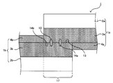
- the first conductive substrate 1a and the second conductive substrate 1b include a surface of the first conductive substrate 1a on the first adhesive layer 4a side, and the second conductive substrate. 1b has a joint portion 17 arranged on the second adhesive layer 4b side so as to face each other.
- the first conductive substrate 1a and the second conductive substrate 1b are fixed, and the first porous conductive layer 3a and the second porous conductive layer 3b are electrically connected. is there.
- the joint portion 17 is formed at each end of the first conductive substrate 1a and the second conductive substrate 1b.
- the porous conductive layers (3 a and 3 b) are electrically connected by forming connection terminal portions 18 at portions corresponding to the joint portions 17 and connecting the connection terminal portions 18 to each other.
- connection terminal portions 18 are electrically connected by forming connection terminal portions 18 at portions corresponding to the joint portions 17 and connecting the connection terminal portions 18 to each other.
- the description of the adhesive layer is omitted for ease of explanation.
- the conductive substrates are disposed by placing the conductive substrates so that the porous conductive layers face each other with the adhesive layer interposed therebetween, and performing pressure bonding or the like. It is possible to form a joint portion in which the members are stably fixed and electrically connected. For this reason, it can be set as the laminated body which has a junction part to which the electrically conductive board
- the porous conductive layer is porous
- the conductive substrates are arranged so that the porous conductive layers face each other with the adhesive layer interposed therebetween, and the conductive substrates are stably bonded by pressing.
- the reason why the bonded and electrically connected joint can be formed is not clear, but is presumed as follows.
- the porous conductive layer in the second embodiment is porous, it has pores. For this reason, when the conductive substrates are arranged so that the porous conductive layers face each other with the adhesive layer interposed therebetween, and pressure bonding is performed, the components derived from the adhesive layer such as the adhesive material constituting the adhesive layer are porous conductive layers. It is possible to flow into the pores of the bed.
- the porous conductive layer at the joint is also closely attached with sufficient adhesive force. can do. For this reason, it can be set as the state which adhered between the conductive substrates stably in the junction part. More specifically, as illustrated in FIG.
- the adhesive material derived from the first and second adhesive layers (4a and 4b) can penetrate into the pores 13 of the first and second porous conductive layers (3a and 3b).
- adhesion between the adhesive materials (14a) that have entered the pores 13 of the two porous conductive layers or adhesion between the adhesive material (14b) that has entered the pores 13 of one conductive layer and the other porous conductive layer The first and second conductive substrates (1a and 1b) can be stably fixed.
- the porous conductive layer is porous, the conductive substrates are placed so that the conductive layers are opposed to each other with the adhesive layer interposed therebetween, and the conductive substrates are stably bonded. Joints that are fixed and electrically connected can be formed.
- the conductive layer of the conductive substrate is a vapor-deposited metal layer or the like that does not have pores, and the conductive layers are brought into contact with each other by pressure bonding or the like, the bonding of an adhesive material or the like The component derived from the layer is pushed away around the portion where the pressure bonding or the like is performed, and there is a possibility that the conductive substrates cannot be fixed with sufficient strength.
- the joint portion can be formed only by pressure bonding or the like, it is possible to eliminate the need for bonding with solder, an anisotropic conductive adhesive, or the like. As a result, problems such as deformation of the substrate due to the use of solder can be prevented. From such a thing, a laminated body can be made excellent in shape stability. In addition, it is possible to eliminate the problem of thickening the laminated body, the accompanying decrease in flexibility of the laminated body, and the increase in cost, which are problems when bonding using an anisotropic conductive adhesive. For this reason, it is possible to obtain a laminate that is thin, excellent in flexibility, and can be formed at low cost.
- the metal particles may be sintered and fused.
- metal particles are sintered at a low temperature when the particle diameter is reduced.
- the metal particles are sintered at a low temperature by utilizing the property of sintering at a temperature much lower than the melting point of the metal particles.
- a layer can be formed. Therefore, there is little damage to the substrate, and it is not necessary to use a substrate having high heat resistance, and a substrate having low heat resistance can also be used.
- an inexpensive general-purpose plastic resin substrate such as polyethylene terephthalate can be used.
- the porous conductive layer can be formed, for example, by applying a metal particle dispersion containing metal particles on a base material and baking it, and has good adhesion to the base material.
- a porous conductive layer can be obtained. Therefore, it is not necessary to form another layer on the base material or to perform surface treatment in order to improve adhesion.
- an adhesive layer is formed on the porous conductive layer.
- the conductive material such as a metal constituting the porous conductive layer in the conductive substrate can be protected with the component derived from the adhesive layer such as the adhesive material contained in the adhesive layer.
- the oxidation of the porous conductive layer can be suppressed. Therefore, it can be set as the laminated body by which the electroconductive fall of the porous conductive layer was suppressed.
- both the conductive substrates also have the adhesive layer on the porous conductive layer, it is possible to obtain a laminate in which the decrease in the conductivity of the porous conductive layer is particularly suppressed.
- the laminate of the second embodiment has a first conductive substrate, a second conductive substrate, and a joint.
- first conductive substrate a first conductive substrate
- second conductive substrate a second conductive substrate
- joint a joint
- the conductive substrate used in the second embodiment includes a first conductive substrate and a second conductive substrate.
- the first conductive substrate and the second conductive substrate include a base material (first base material and second base material), a porous conductive layer (first porous conductive layer and second porous conductive layer), and an adhesive layer. (First adhesive layer and second adhesive layer).
- Porous conductive layer The porous conductive layer is formed on one surface of the substrate.
- the porous conductive layer includes the first porous conductive layer and the second porous conductive layer.
- the porous conductive layer may be formed on the entire surface of the substrate, but is preferably formed in a pattern. This is because it is easy to use the porous conductive layer as a wiring layer because the porous conductive layer is formed in a pattern shape in plan view. This is because the laminate can be made excellent in functionality.
- the use as a wiring layer includes use as an antenna. 2 and 3 which have already been described show an example in which the porous conductive layer is formed in a pattern shape in plan view.
- connection terminal portion is formed in a portion corresponding to the joint portion. This is because electrical connection between the first porous conductive layer and the second porous conductive layer is easy. About the shape of such a connection terminal part, it can be made to be the same as that of the connection terminal in a general conductive substrate. 2 and 3 which have already been described show an example in which the porous conductive layer has a connection terminal portion.
- FIG. 1 is a process diagram showing an example of a method for forming a porous conductive layer.
- the porous conductive layer is formed by preparing the substrate 2, applying the metal particle dispersion 13 a on the substrate 2 (FIG. 14A), and then the substrate 2.
- a coating film containing metal particles is formed by drying the upper metal particle dispersion 13a by heating h (FIG. 14B), and then surface wave plasma treatment is applied to the coating film 13b.
- the metal particles contained in the coating film 13b are sintered together (FIG. 14 (c)), thereby obtaining a porous conductive layer 3 (FIG. 14 (d)). .
- first porous conductive layer and the second porous conductive layer The detailed description of the material, porosity, thickness, formation method, and the like of the first porous conductive layer and the second porous conductive layer is described in the section “A. First Embodiment” above. Since it can be the same as the description regarding 1 porous conductive layer, description here is abbreviate
- Adhesive layer The adhesive layer is formed on the surface of the porous conductive layer opposite to the substrate.
- the adhesive layer has a function of fixing the first conductive substrate and the second conductive substrate at the joint.
- the adhesive layer includes the first adhesive layer and the second adhesive layer.
- the adhesive layer is capable of fixing the first conductive substrate and the second conductive substrate at the joint and electrically connecting the first porous conductive layer and the second porous conductive layer. It is preferable to have a film thickness. Specifically, the thickness of the adhesive layer is more preferably 0.5 ⁇ m or more and 5 ⁇ m or less. This is because, when the film thickness is within the above-described range, it is possible to form a joint portion in which the first conductive substrate and the second conductive substrate are stably fixed and electrically connected.
- the film thickness of the adhesive layer includes the film thickness of the porous conductive layer. Specifically, it is shown by a in FIG.
- the first conductive substrate at the joint portion can be fixed, and it is preferable that the first porous conductive layer and the second porous conductive layer can be electrically connected, and the thickness of the adhesive layer is the same. Can do.
- the adhesive layer may not enter the pores of the porous conductive layer, or may enter the pores of the porous conductive layer. Further, when the adhesive layer enters the pores of the porous conductive layer, the adhesive layer can be in a state where it does not fill all the pores of the porous conductive layer.
- the method for forming the adhesive layer is not particularly limited as long as it can form an adhesive layer having a desired film thickness.
- the forming method include, when the adhesive material is a thermoplastic resin, a method in which a material obtained by heating and melting the material of the adhesive layer is applied onto the porous conductive layer and then solidified by cooling. be able to.
- the method similar to the coating method of the said metal particle dispersion liquid can be used.
- the adhesive material is a thermosetting resin or a photosensitive resin whose adhesiveness or adhesiveness is reduced by irradiation with light
- the adhesive layer is one that is cured by heating or light irradiation except for the joint. May be.
- the base material supports the porous conductive layer and the adhesive layer.
- the base material includes a first base material and a second base material.
- the conductive substrate has a base material, a porous conductive layer, and an adhesive layer, it may have another structure as needed.
- the conductive substrate includes the first conductive substrate and the second conductive substrate.
- the method for producing the conductive substrate may be any method as long as the substrate, the porous conductive layer, and the adhesive layer can stably form a conductive substrate laminated in this order, and the porous conductive layer is formed on the substrate.
- a method for forming an adhesive layer can be used later.
- a method for producing a conductive substrate when the porous conductive layer has a pattern shape a method of applying a metal particle dispersion in a pattern shape may be used, but the porous conductive layer is formed on the entire surface of the substrate.
- a method may be used in which the formed base material for a conductive substrate is prepared, and the porous conductive layer is removed by heat transfer at a place other than the place to be left in a pattern.
- FIG. 15 is a process diagram showing an example of a method for producing a conductive substrate having a patterned porous conductive layer.
- FIG. 15 shows an example in which the adhesive material is a thermoplastic resin.
- a method for manufacturing a conductive substrate includes preparing a base material 2 for a conductive substrate in which a base material 2, a porous conductive layer 3 and an adhesive layer 4 are laminated in this order, and a transfer substrate 21. (FIG. 15 (a)), in a state where the adhesive layer 4 of the substrate for conductive substrate 1X and the transfer substrate 21 are in contact with each other, a portion of the porous conductive layer 3 other than the portion to be left in a pattern is removed from the thermal head.
- the porous conductive layer 3 is transferred to the transfer substrate 21 side together with the adhesive layer 4 by heating with a heating body 22 such as a thermal head of the printer, and the adhesive layer 4 is not heated and has low adhesiveness or adhesiveness. Only the low adhesion portion is left on the base material 2 (FIG. 15B), and after the heated portion is cooled, the transfer substrate 21 is peeled off to obtain the conductive substrate 1 having the patterned porous conductive layer 3. It can be set as a method (FIG.15 (c)). In this method, the adhesive layer 4 is also formed in the same pattern as the porous conductive layer 3.
- the adhesive material is a thermosetting resin or a photosensitive resin whose adhesiveness or adhesiveness is reduced by light irradiation.
- the low adhesion part with low adhesiveness or adhesiveness by heating or irradiating the porous conductive layer of the remaining part, transfer the unheated or unirradiated part to the transfer substrate by contacting the transfer substrate.
- the light irradiation method include a method of exposing through a pattern composed of a light shielding portion such as a photomask and an opening, a direct drawing method using a laser, and the like.
- the porous conductive layer is porous, brittleness is imparted, and unlike conventional vapor deposition layers, there are few burrs during transfer, and large crystal grains are not included. Therefore, the porous conductive layer can obtain good foil breakability. For this reason, as shown in FIG. 5 which has already been described, it is possible to transfer with good resolution by heating the porous conductive layer at a place other than the place left in the pattern and transferring it to the transfer substrate.
- the porous conductive layer can allow the component derived from the adhesive layer, for example, the adhesive material contained in the adhesive layer, to enter the pores, and apparently the component derived from the porous conductive layer and the adhesive layer. Therefore, thermal diffusion can be made difficult to occur. Therefore, when transferring the porous conductive layer to the transfer substrate, it is difficult for heat to escape, so there is no need to heat excessively, which is advantageous for thermal transfer.
- the component derived from the adhesive layer can be introduced into the pores of the porous conductive layer, not only the surface area of contact between the porous conductive layer and the adhesive layer is increased, but also the anchor The adhesion between the porous conductive layer and the adhesive layer can be enhanced by the effect. Therefore, when the porous conductive layer is transferred to the transfer substrate, the adhesive layer and the porous conductive layer can be satisfactorily transferred to the transfer substrate, and excellent transferability can be obtained.
- the bonding portion in the second embodiment includes the surface of the first conductive substrate and the second conductive substrate on the first adhesive layer side of the first conductive substrate and the second adhesive layer of the second conductive substrate. It is a site
- being fixed means that the second conductive substrate and the second conductive substrate are fixed by being in close contact with each other.
- the peel strength between the two conductive substrates is such that the first conductive substrate and the second conductive substrate can be maintained in electrical connection between the first porous conductive layer and the second porous conductive layer when the laminate is manufactured and used.
- the peel strength is preferably such that the two conductive substrates are not separated.
- being electrically connected means that the first porous conductive layer and the second porous conductive layer are in contact with each other and are in a state where electricity can be passed.
- the first porous conductive layer and the second porous conductive layer are so large that the laminate of the second embodiment can perform a desired function.
- the conductive conductive layer is preferably in contact.
- both the conductive substrates are stably fixed, and
- the conductive layer is preferably a portion where the two conductive layers can be electrically connected, and preferably the end portions of the first conductive substrate and the second conductive substrate. This is because the formation of the joint is easy.
- the area of the joint is preferably an area that can stably fix the first conductive substrate and the second conductive substrate, and is appropriately set according to the type of the laminate, the size of the conductive substrate, and the like. Is.
- the laminated body according to the second embodiment includes the first conductive substrate, the second conductive substrate, and the bonding portion, but may have other configurations as necessary.
- the laminate of the second embodiment includes a printed wiring board, an electromagnetic shielding material, an antenna, a power semiconductor, a noise filter, a capacitor electrode, and various sensor electrodes (touch sensor, biosensor, temperature sensor, gas sensor). , Optical sensor, pressure sensor, flow sensor), display electrode, solar cell electrode, IC card, RFID, and the like, and can be used for bonding materials and connector materials.
- the laminate of the second embodiment can be used as an electromagnetic wave shielding layer for preventing unauthorized reading of information recorded on a non-contact type IC card, and a conductive layer for modulating the resonance frequency.
- a porous conductive layer can be applied to a part of the card and transported in a state where reading cannot be performed, and the adhesive layer can be scratched and removed at the time of use. Since the laminate of the second embodiment has a porous conductive layer, it can be easily peeled off by scratching by controlling the adhesive force of the adhesive layer.
- the manufacturing method of the laminated body is not particularly limited as long as it is a method capable of stably fixing and electrically connecting the first conductive substrate and the second conductive substrate.
- the manufacturing method for example, the first conductive substrate and the second conductive substrate are arranged such that the first and second porous conductive layers face each other with the first and second adhesive layers interposed therebetween, and are subjected to pressure bonding or the like.
- a method can be mentioned.
- FIG. 16 is a process diagram showing an example of a method for manufacturing a laminate according to the second embodiment.
- FIG. 16 shows an example in which the adhesive material is a thermoplastic resin. As illustrated in FIG.
- the first conductive substrate 1 a and the second conductive substrate 1 b are prepared, and the first conductive substrate 1 a and the second conductive substrate 1 b are joined to the joint portion 17. Is disposed so that the first and second porous conductive layers (3a and 3b) are opposed to each other through the first and second adhesive layers (4a and 4b) and then contacted with each other.
- a process (FIG. 16A), a bonding process of heating and pressurizing a portion where the joint portion 17 of the first conductive substrate 1a and the second conductive substrate 1b is formed using the heating body 22 (FIG.
- a cooling step (not shown) for cooling a portion where the joint portion 17 of the first conductive substrate 1a and the second conductive substrate 1b is formed, and the first conductive substrate 1a and the second conductive substrate 1b
- First porous conductive layer 3a and second porous Conductive layer 3b can be made to obtain a laminated body 10 having a joint 17 which is electrically connected (FIG. 16 (c)).
- the reference numerals in FIG. 16 indicate the same members as those already described in FIG. 11 and FIG.
- the adhesive material is a thermosetting resin or a photosensitive resin whose adhesiveness or adhesiveness is reduced by light irradiation
- the joining step can crimp a portion where the joint is formed.
- the bonding step may be one in which the bonding portion is heated or irradiated with light, or may be one in which the entire first conductive substrate and the second conductive substrate arranged opposite to each other are heated or irradiated with light.
- the joining step may be one that is heated together with light irradiation.
- the thermoplastic resin as the adhesive material contained in the first and second adhesive layers has fluidity as the heating temperature when the first and second conductive substrates are thermocompression bonded together. It is preferable that the temperature is higher than or equal to the temperature that can be shown, and can be appropriately set according to the types of the first and second adhesive layers.
- the pressure applied when the conductive substrates are pressure-bonded or the like is such that the first porous conductive layer and the second porous conductive layer can be brought into contact by flowing the adhesive material contained in the adhesive layer. It may be sufficient, and can be appropriately set according to the types of the first and second adhesive layers, the heating temperature, and the like.
- a laminate of the third embodiment includes a first base material, a first porous conductive layer on one surface of the first base material, and the first base of the first porous conductive layer.
- a surface of the conductive substrate on the side of the first adhesive layer and a surface of the third conductive substrate on the side of the third porous conductive layer are disposed so as to face each other.
- the substrate and the third conductive substrate are fixed to each other, and the first porous conductive layer and the third porous conductive layer are electrically connected to each other.
- the first base material and the third base material are simply referred to as the base material
- the first porous conductive layer and the third porous conductive layer are simply referred to as the porous conductive layer
- the first adhesive layer and the first base material In some cases, the three adhesive layers are simply referred to as adhesive layers
- the first conductive substrate and the third conductive substrate are simply referred to as conductive substrates.
- FIG. 17A and FIG. 17B are schematic cross-sectional views showing an example of the laminated body of the third embodiment.
- the laminate 1 of the third embodiment includes a first base 2a and a first porous formed on one surface of the first base 2a.
- a first conductive substrate 1a having a first adhesive layer 4a formed on the surface of the conductive conductive layer 3a and the first porous conductive layer 3a opposite to the first base 2a, and a third base 2c
- the third porous layer formed on the surface opposite to the third base material 2c of the third adhesive layer 4c and the third adhesive layer 4c formed on one surface of the third base material 2c.
- a third conductive substrate 1c having a conductive layer 3c wherein the first conductive substrate 1a and the third conductive substrate 1c are a surface of the first conductive substrate 1a on the first adhesive layer 4a side, and A surface of the third conductive substrate 1c on the side of the third porous conductive layer 3c has a bonding portion 17 disposed so as to face the surface.
- the first conductive substrate 1a and the third conductive substrate 1c are fixed, and the first porous conductive layer 3a and the third porous conductive layer 3c are electrically connected.
- the joint portion 17 is formed at the ends of the first conductive substrate 1a and the third conductive substrate 1c.
- the conductive substrates are disposed by placing the conductive substrates so that the porous conductive layers face each other with the adhesive layer interposed therebetween, and performing pressure bonding or the like. It is possible to form a joint portion in which the members are stably fixed and electrically connected. For this reason, it can be set as the laminated body which has a junction part to which the electrically conductive board
- adheresion is sufficient if the first conductive substrate 1a and the third conductive substrate 1c are in contact with each other, for example, as shown in FIG. Therefore, for example, as shown in FIG. 17B, the case where the first conductive substrate 1a and the third conductive substrate 1c are in contact with each other is also included.
- the porous conductive layer is porous, the conductive substrates are disposed so that the porous conductive layers face each other with an adhesive layer interposed therebetween, and the conductive substrates are stably fixed by pressure bonding or the like.
- the reason why an electrically connected joint can be formed is not clear, but is presumed as follows.
- the porous conductive layer in the third embodiment is porous, it has pores. For this reason, when the conductive substrates are arranged so that the porous conductive layers face each other through the adhesive layer, and the pressure bonding or the like is performed, the adhesive material constituting the adhesive layer flows into the pores of the porous conductive layer. Is possible.
- the porous conductive layers are in an electrically connected state in contact with each other at a location where crimping or the like is performed, the adhesive materials that have flowed into the pores of the opposing porous conductive layers Due to the close contact and the close contact between the adhesive material flowing into the pores of one porous conductive layer and the other porous conductive layer, the conductive substrates can be brought into a fixed state.
- the adhesive material of the first adhesive layer is: Adhesion of adhesive materials that can enter the pores of the first and third porous conductive layers, and the pores of both porous conductive layers, or the pores of one porous conductive layer
- the conductive substrates can be fixed to each other. Therefore, when the porous conductive layer is porous, the conductive substrates are arranged so that the porous conductive layers face each other with the adhesive layer interposed therebetween, and are subjected to pressure bonding or the like.
- the joint portion can be formed only by pressure bonding or the like, it is possible to eliminate the need for bonding with solder, an anisotropic conductive adhesive, or the like. As a result, it is possible to obtain a laminated wiring board that is excellent in shape stability between conductive substrates, is thin, has excellent flexibility, and can be formed at low cost.
- metal particles may be sintered and fused.
- the metal particles are sintered at a low temperature to form a porous conductive layer by utilizing the property that when the metal particles become nanoparticles, the metal particles are sintered at a temperature much lower than the melting point of the metal particles. can do. Therefore, there is little damage to the substrate, and it is not necessary to use a substrate having high heat resistance, and a substrate having low heat resistance can also be used.
- the porous conductive layer can be formed, for example, by applying a metal particle dispersion containing metal particles on a base material and baking it, and has good adhesion to the base material.
- a porous conductive layer can be obtained. Therefore, it is not necessary to form another layer on the base material or to perform surface treatment in order to improve adhesion.
- the first conductive substrate in the third embodiment has an adhesive layer formed on the conductive layer. For this reason, the electroconductive fall of a porous conductive layer can be suppressed. Therefore, it can be set as the laminated body by which the electroconductive fall of the porous conductive layer was suppressed.
- the laminate of the third embodiment has a first conductive substrate and a third conductive substrate.
- first conductive substrate and a third conductive substrate.
- the conductive substrate used in the third embodiment includes a first conductive substrate and a third conductive substrate.
- the first conductive substrate and the third conductive substrate include a base material (first base material and third base material), a porous conductive layer (first porous conductive layer and third porous conductive layer), and an adhesive layer. (First adhesive layer and third adhesive layer).
- the method for producing the third conductive substrate is not particularly limited as long as it is a method capable of accurately obtaining the third conductive substrate in which the third base material, the third adhesive layer, and the third porous conductive layer are laminated in this order. It is not a thing.
- a method for producing such a third conductive substrate for example, a transfer substrate in which a transfer base material, a porous conductive layer and an adhesive layer are laminated in this order, and a base material are prepared.
- a method for transferring the porous conductive layer to the substrate can be mentioned.
- the adhesive material is a thermoplastic resin, more specifically, as illustrated in FIG. 2, the transfer base material 32, the porous conductive layer 3 and the adhesive layer 4 are laminated in this order.
- the transfer substrate 31 is prepared, and the opposing placement step in which the adhesive layer 4 of the transfer substrate 31 and the base material 2 are placed so as to face each other and contact each other (FIG. 18A), and the transfer substrate 31 and the base material 2 are heated. And a heating and pressurizing step for pressurization (FIG. 18B), a cooling step for cooling the transfer substrate 31 and the base material 2 (not shown), and then a transfer base material 32 included in the transfer substrate 31 Can be used to obtain a third conductive substrate 1c in which the third base material 2c, the third adhesive layer 4c, and the third porous conductive layer 3c are laminated in this order (FIG. 18C). )). Moreover, since the reference numerals in FIG.
- the adhesive material is a thermosetting resin or a photosensitive resin whose adhesiveness or adhesiveness is reduced by light irradiation
- a pressurizing step of pressurizing the transfer substrate and the base material after the opposing placement step is performed as the manufacturing method. The method of doing can be used.
- the third adhesive layer and the third porous conductive layer can be formed on the third base material by using the transfer method as described above.
- a substrate that has conventionally been difficult to form a porous conductive layer can also be used. Therefore, it is possible to obtain a conductive substrate in which a porous conductive layer is formed on a resin base material of inexpensive general-purpose plastic such as polyethylene terephthalate or a paper base material.
- the base material (1st base material and 3rd base material) which comprises a 1st conductive substrate and a 3rd conductive substrate, a porous conductive layer (a 1st porous conductive layer and a 3rd porous conductive layer), and adhesion
- the other description of the layers can be the same as the contents described in the above-mentioned section “B. Second embodiment 1. Conductive substrate”. Is omitted.
- the bonding portion in the third embodiment includes the surface of the first conductive substrate and the third conductive substrate on the first adhesive layer side of the first conductive substrate and the third porosity of the third conductive substrate. This is a portion where the surface on the conductive layer side is arranged to face each other. Further, in the joint portion, the first conductive substrate and the third conductive substrate are fixed, and the first porous conductive layer and the third porous conductive layer are electrically connected. It is. Specifically, for example, as illustrated in FIG. 17A, the bonding portion includes a first porous conductive layer 3 a and an electrically connected first conductive substrate 1 a and a third conductive substrate 1 c. As shown in FIG.
- the third porous conductive layer 3c overlaps in plan view and is electrically connected between the first conductive substrate 1a and the third conductive substrate 1c.
- the first porous conductive layer 3a and the third porous conductive layer 3c overlap each other in a plan view and include an integral part.
- the laminated body according to the third embodiment includes the first conductive substrate and the third conductive substrate, but may have other configurations as necessary.
- the protective layer which covers a 3rd porous conductive layer can be mentioned, for example. This is because a decrease in conductivity of the porous conductive layer can be suppressed.
- the 3rd porous conductive layer in a junction part is a thing which is not normally covered with a protective layer. Therefore, when the protective layer is formed on the third porous conductive layer before forming the joint portion, the protective layer is formed except for a portion where the joint portion of the third porous conductive layer is formed.
- the protective layer of the location in which a junction part is formed is removed and used.
- a material which comprises the said protective layer it is preferable to have insulation, For example, it can be set to the same as that of the said base material.
- Method for Producing Laminate The method for producing the laminate can be the same as that described in the above section “B. Second Embodiment 5. Method for Producing Laminate”, so the explanation here is as follows. Omitted.
- the manufacturing method of the electroconductive base material of this indication WHEREIN: The manufacturing process of the electroconductive base material of this indication WHEREIN: The preparation process which prepares a laminated body, and the 1st contact bonding layer and 1st porous conductive layer of the said laminated body on a to-be-transferred base material. And a transfer process for transferring.
- the first adhesive layer used in the method for producing a conductive substrate of the present disclosure is formed on the first porous conductive layer, and the first porous layer is transferred when the laminate is transferred to the transfer substrate. It is preferable to have a function of adhering the conductive conductive layer and the substrate to be transferred.
- the first adhesive layer used in the method for manufacturing a conductive substrate according to the present disclosure may be, for example, a pressure-sensitive adhesive layer or may not be a pressure-sensitive adhesive layer.
- an embodiment in which the first adhesive layer is not a pressure-sensitive adhesive layer will be described as a first embodiment, and an embodiment in which the first adhesive layer is a pressure-sensitive adhesive layer will be described separately as a second embodiment.
- the method for producing a conductive substrate according to the first embodiment has two embodiments.
- the first A embodiment and the first B embodiment will be described separately.
- the manufacturing method of the electroconductive base material of 1st embodiment is the electroconductive base material using the laminated body described in the item of "I. Laminate A. 1st embodiment 1. 1A embodiment" mentioned above. It corresponds to the manufacturing method.
- the manufacturing method of the electroconductive base material of 1A embodiment is the preparatory process which prepares the laminated body described in the above-mentioned "I. Laminated body A. 1st embodiment 1. 1A embodiment.” And a transfer step of transferring the adhesive layer and the porous conductive layer of the laminate onto the substrate to be transferred.
- FIGS. 2 (a) to 2 (c) and FIGS. 3 (a) to 3 (c) are process diagrams showing an example of a method for producing a conductive substrate according to the first embodiment. 2 (a) to 2 (c) and FIGS. 3 (a) to 3 (c) are described in detail in the above “I. Laminate A. First embodiment 1. First A embodiment”. Therefore, the description here is omitted.
- the component derived from the first adhesive layer for example, the resin contained in the first adhesive layer
- the component derived from the first adhesive layer can be introduced into the pores of the first porous conductive layer.
- thermal diffusion can be made difficult to occur. Therefore, in the transfer step, heat is difficult to escape, so there is no need to heat excessively, which is advantageous for thermal transfer.
- the component derived from the first adhesive layer can be introduced into the pores of the first porous conductive layer, and the first porous conductive layer and the first adhesive layer Adhesion can be increased. Therefore, in the transfer step, the first adhesive layer and the first porous conductive layer can be satisfactorily transferred onto the transfer substrate, and excellent transferability can be obtained.
- the resin contained in the first adhesive layer can enter the pores of the first porous conductive layer, in the transfer step, the first porous conductive layer is used. Can be protected by the resin contained in the first adhesive layer, and oxidation of the first porous conductive layer can be suppressed. Therefore, it is possible to suppress a decrease in conductivity of the first porous conductive layer in the transfer process.
- the laminate since the laminate has the first porous conductive layer, the foil cutting property is good, and the first adhesive layer and the first porous conductive layer of the laminate are provided on the substrate to be transferred. It can transfer well. Further, as illustrated in FIGS. 3A to 3C, when transferring the pattern of the first adhesive layer and the first porous conductive layer of the laminate onto the transfer substrate, the resolution is high. Can be transferred.
- the first adhesive layer and the first porous conductive layer are transferred onto the substrate to be transferred, there are also substrates that have conventionally been difficult to form the first porous conductive layer as the substrate to be transferred. Can be used. Therefore, it is possible to obtain a conductive base material in which a first porous conductive layer is formed on an inexpensive general-purpose plastic resin base material such as polyethylene terephthalate or a transfer base material such as a paper base material. Furthermore, it is possible to form the first porous conductive layer on the substrate to be transferred which is a three-dimensional object. Moreover, a conductive base material can be easily produced only by transferring a 1st contact bonding layer and a 1st porous conductive layer on a to-be-transferred base material.
- the first porous conductive layer can be formed by sintering metal particles at a low temperature, it is necessary to use a highly heat-resistant substrate as the first substrate of the laminate.
- a substrate having low heat resistance can also be used.
- an inexpensive general-purpose plastic resin substrate such as polyethylene terephthalate can be used. Therefore, the manufacturing cost can be reduced.
- the preparatory process in 1A embodiment is a process of preparing the above-mentioned laminated body.
- description here is abbreviate
- Transfer process is a process of transferring the first adhesive layer and the first porous conductive layer of the laminate onto the substrate to be transferred.
- the substrate to be transferred is not particularly limited as long as the first porous conductive layer can be transferred through the first adhesive layer, and is appropriately selected according to the use of the conductive substrate. Is done.
- a resin base material, a paper base material, a glass base material, a metal base material, etc. are mentioned.
- the first adhesive layer and the first porous conductive layer of the laminate onto the substrate to be transferred it is possible to adhere the first adhesive layer to a predetermined position on the substrate to be transferred. If it is not specifically limited, it will select suitably according to the material of a 1st contact bonding layer.
- examples of the thermal transfer method include a method using a heating roller or a hot stamp, a hot pressing method, and the like.
- examples of the thermal transfer method include a method using a mold as illustrated in FIGS. 19 (a) to 19 (d).
- a laminate 1 as shown in FIG. 19A is prepared.
- the laminated body 1 is the same as the laminated body 1 shown in FIG.
- the first adhesive layer 4 a of the laminate 1 and the transferred substrate 11 are laminated so that the laminate 1 and the transferred substrate 11 are laminated.
- the first base 2a is placed in a molding die having an upper die 43a and a lower die 44a so that the first base 2a faces the upper die 43a and the transferred substrate 11 faces the lower die 44a.
- the mold 1 is heated and clamped to mold the laminate 1 and the transfer substrate 11, and at the same time, the laminate 1 is thermally transferred to the transfer substrate 11. .
- the to-be-transferred base material 11 and the laminated body 1 are integrated.
- the integrated laminate 1 and the substrate to be transferred 11 are taken out from the mold, and as shown in FIG. 19 (d), the first substrate 2a from the laminate 1 is obtained. To peel off.
- stacked in order on the to-be-transferred base material 11 is obtained.
- thermoplastic resin as illustrated in FIGS. 3A to 3C, when the pattern of the first adhesive layer and the first porous conductive layer is thermally transferred onto the transfer substrate.
- thermal transfer method include a method using a laser beam or a thermal head.
- the first adhesive layer of the laminate is irradiated with light in a pattern, and the laminate and the substrate to be transferred are brought into close contact with each other.
- the method of peeling the side is mentioned.
- a transfer method as shown in FIGS. 6A to 6D can be applied.
- the pattern of the first adhesive layer and the first porous conductive layer can be transferred onto the transfer substrate.
- Examples of the method of irradiating the first adhesive layer with light in a pattern include a method using a photomask and a method of drawing light using a laser or the like.
- the light applied to the first adhesive layer is not particularly limited as long as it can reduce the tackiness or adhesiveness of the first adhesive layer, and is appropriately selected according to the type of the photosensitive resin.
- the For example, ultraviolet rays, visible rays, infrared rays, etc. can be used.
- Examples of the method for bringing the laminate and the substrate to be transferred into close contact include a method of applying pressure and a method of applying pressure while heating.
- the patterns of the first adhesive layer and the first porous conductive layer may be transferred onto the substrate to be transferred.
- a conductive base material in which a pattern of the first porous conductive layer is formed on the transfer base material can be obtained.
- thermoplastic resin When a thermoplastic resin is used and the pattern of the first adhesive layer and the first porous conductive layer is thermally transferred onto the substrate to be transferred, a method using a laser beam or a thermal head as described above may be applied.
- the laminate 1 in which the first adhesive layer 4a as illustrated in FIG. 5A is formed in a pattern in advance may be used, and the first adhesive layer 4a as illustrated in FIG.
- the laminate 1 on which the non-first adhesive layer 5 is formed in a pattern may be used.
- the pattern of the first porous conductive layer is thermally transferred onto the substrate to be transferred, in addition to the above, the first porous conductive layer 3a as illustrated in FIG. You may use the laminated body 1 formed in this.
- the laminate and the substrate to be transferred are placed in the mold, the laminate and the substrate are placed on the mold.
- the transfer substrate may be vacuum-sucked so that the laminate and the transferred substrate conform to the shape of the mold, and after the laminate and the transferred substrate are laminated, they are heated and softened. And may be sandwiched between molds.
- the first adhesive layer is usually adhered on the transferred substrate by physically separating the laminate from the substrate side. In the region, the substrate can be peeled from the first porous conductive layer.
- the substrate of the laminate is peeled from the molded product. In the case of a long laminate, the substrate is peeled from the laminate when a molded product in which the laminate and the transferred substrate are integrated is taken out of the mold.
- the manufacturing method of the electroconductive base material of 1B embodiment is the preparatory process of preparing the laminated body described in the above-mentioned "I. Laminated body A. 1st embodiment 1. 1A embodiment.” And placing the laminate on a mold, injecting a molten resin for a substrate to be transferred into the mold and solidifying it to mold the substrate to be transferred, and simultaneously forming the laminate on the substrate to be transferred It is a manufacturing method which has the shaping
- FIG. 20 (a) to 20 (d) are process diagrams showing an example of a method for producing a conductive substrate according to this embodiment.
- the laminated body 1 as shown to Fig.20 (a) is prepared.
- the laminated body 1 is the same as the laminated body 1 shown in FIG.
- the laminate 1 is placed in a molding die having a fixed die 41 and a movable die 42 so that the first base material 2 a faces the fixed die 41. Subsequently, as shown in FIG.
- the mold is clamped, and the transfer base material molten resin 11a is injected into the mold, cooled and solidified, and simultaneously with the transfer base material being molded. Then, the laminate 1 is transferred to the substrate to be transferred. Thereby, the to-be-transferred base material which is a resin molding and the laminated body 1 are laminated
- the integrated laminate 1 and the substrate to be transferred 11 are taken out from the mold, and as shown in FIG. 20 (d), the first substrate 2a is taken out of the laminate 1. To peel off. Thereby, the electroconductive base material 10 by which the 1st contact bonding layer 4a and the 1st porous electroconductive layer 3a were laminated
- the component derived from the first adhesive layer for example, the resin contained in the first adhesive layer
- the component derived from the first adhesive layer can be introduced into the pores of the first porous conductive layer.
- thermal diffusion can be made difficult to occur. Therefore, in the molding and transfer process, heat does not easily escape, so it is not necessary to heat excessively, which is advantageous for transfer.
- the component derived from the first adhesive layer can be introduced into the pores of the first porous conductive layer, and the first porous conductive layer and the first adhesive layer Adhesion can be increased. Therefore, in the molding and transfer process, the first adhesive layer and the first porous conductive layer can be satisfactorily transferred onto the transfer target substrate, and excellent transferability can be obtained.
- the resin contained in the first adhesive layer can enter the pores of the first porous conductive layer, the first porous layer is formed in the molding and transfer process.
- the conductive layer can be protected with the resin contained in the first adhesive layer, and oxidation of the first porous conductive layer can be suppressed. Therefore, it is possible to suppress a decrease in conductivity of the first porous conductive layer in the molding and transfer process.
- the transferred substrate that is a resin molded body and the laminate are laminated and integrated, it is possible to form the first porous conductive layer on the transferred substrate that is a three-dimensional object. It is.
- the laminate since the laminate has the first porous conductive layer, the foil cutting property and the resolution are good. Therefore, for example, when the laminate 1 as shown in FIGS. 5A and 5B is used, the transfer can be performed with good foil breakage and high resolution.
- the first porous conductive layer can be formed by sintering metal particles at a low temperature, it is necessary to use a highly heat-resistant substrate as the first substrate of the laminate.
- a substrate having low heat resistance can also be used.
- an inexpensive general-purpose plastic resin substrate such as polyethylene terephthalate can be used. Therefore, the manufacturing cost can be reduced.
- the preparatory process in 1B embodiment is a process of preparing the above-mentioned laminated body.
- a thermoplastic resin is used as the material of the first adhesive layer.
- the laminate is placed in a mold, the molten resin for the substrate to be transferred is injected into the mold, solidified, and transferred. This is a step of transferring the laminate to the substrate to be transferred simultaneously with forming the substrate.
- the laminate When arranging the laminate in the mold, the laminate is arranged so that the first adhesive layer is in contact with the molten resin for the transferred substrate when the molten resin for the transferred substrate is injected into the mold. .
- a sheet stack may be disposed in the mold, and a predetermined region of the long stack may be inserted intermittently.
- the heating temperature is preferably equal to or higher than the glass transition temperature of the first base material of the laminate and less than the melting temperature or the melting point, and is set to a temperature near the glass transition temperature of the first base material. More preferred.
- the vicinity of the glass transition temperature means a range of glass transition temperature ⁇ 5 ° C.
- thermosetting resin includes a two-component curable resin.
- the molten resin for a substrate to be transferred one kind may be used alone, or two or more kinds may be used.
- the molten resin for the substrate to be transferred is a thermoplastic resin
- the thermoplastic resin is injected in a fluid state by heating and melting, and is cooled and solidified.
- the molten resin for a substrate to be transferred is a thermosetting resin
- the uncured resin composition is appropriately heated, injected in a fluid state, and heated to be solidified.
- the heating temperature of the transfer resin for the transfer substrate varies depending on the type of transfer resin for the transfer substrate, but is, for example, about 80 ° C. or more and 280 ° C. or less.
- the pattern of the first adhesive layer and the first porous conductive layer may be transferred to the transfer substrate.
- a conductive base material in which a pattern of the first porous conductive layer is formed on the transfer base material can be obtained.
- a laminate in which the first adhesive layer 4a as illustrated in FIG. 1 may be used, and the laminate 1 in which the non-first adhesive layer 5 is formed in a pattern on the first adhesive layer 4a as illustrated in FIG. 5B may be used.
- the first porous conductive layer 3a as illustrated in FIG. The formed laminate 1 may be used.
- the molded product in which the laminate and the molded substrate to be transferred are integrated is taken out from the mold.
- the peeling process in the 1B embodiment is a process of peeling the base material of the laminate.
- a molded product in which the laminate and the molded substrate to be transferred are integrated is taken out of the mold, and then the first substrate of the laminate is peeled from the molded product.
- the first substrate is peeled from the laminate when a molded product in which the laminate and the molded substrate to be transferred are integrated is taken out from the mold.
- the manufacturing method of the electroconductive base material of 2nd embodiment is the preparatory process which prepares the above-mentioned laminated body, the 1st pressure-sensitive-adhesive layer of the said laminated body, and 1st porosity on a to-be-transferred base material And a transfer step of transferring the pressure by applying pressure to the conductive layer.
- the manufacturing method of the electroconductive base material of 2nd embodiment is the electroconductive base material using the laminated body described in the item of "I. Laminate A. 1st embodiment 2. 1B embodiment" mentioned above. It corresponds to the manufacturing method.
- FIG. 2 (a) to 2 (c), FIG. 3 (a) to FIG. 3 (c), FIG. 4 (a), and FIG. 4 (b) are examples of the method for producing the conductive substrate of the second embodiment.
- the first porous conductive layer and the first pressure-sensitive adhesive layer are Not only the surface area to be bonded is increased, but also the adhesion between the first porous conductive layer and the first pressure-sensitive adhesive layer can be enhanced by the anchor effect. Therefore, in the transfer step, the first pressure-sensitive adhesive layer and the first porous conductive layer can be satisfactorily transferred to the transfer substrate, and excellent transferability can be obtained.
- the pressure-sensitive adhesive and the pressure-sensitive adhesive can be used as the first pressure-sensitive adhesive layer, heating is not required when transferring the laminate onto the substrate to be transferred. It is possible to suppress a decrease in conductivity due to oxidation of the first porous conductive layer, a distortion of the laminated body, and the like.
- the first porous conductive layer is porous, brittleness is imparted. Therefore, unlike the conventional vapor deposited layer, the generation of burrs is small during transfer, and large crystal grains are included. There is nothing. Therefore, good foil breakability can be obtained. Furthermore, as illustrated in FIGS. 9A to 9C, when transferring the pattern of the first pressure-sensitive adhesive layer and the first porous conductive layer of the laminate onto the transfer substrate, Transfer with good resolution. 10A and 10B, the pattern of the first pressure-sensitive adhesive layer and the first porous conductive layer is transferred using a transfer tool by using a strip-shaped laminate. It can be easily transferred onto a substrate.
- the first porous conductive layer can be formed by sintering the metal particles at a low temperature, it is not necessary to use a highly heat-resistant substrate as the substrate of the laminate.
- a substrate having low heat resistance can also be used.
- an inexpensive general-purpose plastic resin substrate such as polyethylene terephthalate can be used. Therefore, the manufacturing cost can be reduced.
- first pressure-sensitive adhesive layer and the first porous conductive layer are transferred onto the transfer substrate, it has been difficult to form the first porous conductive layer as a transfer substrate in the past.
- Materials can also be used. Therefore, it is possible to obtain a conductive base material in which a first porous conductive layer is formed on an inexpensive general-purpose plastic resin base material such as polyethylene terephthalate or a transfer base material such as a paper base material. Furthermore, it is possible to form the first porous conductive layer on the substrate to be transferred which is a three-dimensional object. Moreover, a conductive base material can be easily produced only by pressurizing and transferring the first pressure-sensitive adhesive layer and the first porous conductive layer on the transfer base material.
- the preparatory process in a 2nd embodiment is a process of preparing the above-mentioned laminated body.
- the laminated body since it described in detail in the said "I. laminated body A. 1st embodiment 2. 1B embodiment," description here is abbreviate
- Transfer process is a process of applying pressure to the first pressure-sensitive adhesive layer and the first porous conductive layer of the laminate on the transfer substrate.
- the substrate to be transferred is not particularly limited as long as it can press and transfer the first porous conductive layer through the first pressure-sensitive adhesive layer, and the use of the conductive substrate, etc. It is appropriately selected depending on.
- a resin base material a paper base material, a glass base material, a ceramic base material, a metal base material, etc. are mentioned.
- the first pressure-sensitive adhesive layer is bonded to a predetermined position on the transfer substrate.
- the method is not particularly limited as long as it can be applied, and examples thereof include a method using a roller or a stamp, and a pressing method.
- Examples of the transfer method include a method using an uneven plate and a method of drawing a laminate using a projection such as a needle.
- the pattern of the first pressure-sensitive adhesive layer and the first porous conductive layer is transferred onto the transfer substrate. May be transferred under pressure.
- a conductive base material in which a pattern of the first porous conductive layer is formed on the transfer base material can be obtained.
- the laminate 1 in which the first pressure-sensitive adhesive layer 4a illustrated in FIG. 5A is formed in a pattern in advance may be used, and the first pressure-sensitive adhesive illustrated in FIG. 5B.
- the laminated body 1 in which the non-first pressure-sensitive adhesive layer 5 is formed in a pattern on the layer 4a may be used.
- a strip-shaped laminate may be used as shown in FIG.
- the laminate 1 in which the first porous conductive layer 3a illustrated in FIG. 4A is formed in a pattern in advance may be used.
- the first pressure-sensitive adhesive layer After adhering the first pressure-sensitive adhesive layer of the laminate on the transfer substrate, the first pressure-sensitive adhesive layer is usually separated from the first substrate side by physically separating the laminate from the first pressure-sensitive substrate. In the region where the adhesive layer is bonded, the first substrate can be peeled from the first porous conductive layer.
- the laminate when a flexible material is used as the first substrate of the laminate, the laminate is physically separated from the first substrate side while bending the first substrate. It is preferable because the first substrate can be peeled from the one porous conductive layer and can be easily transferred to a three-dimensional object having a complicated shape such as a curved surface, a stepped shape, or a cornered shape.
- the first pressure-sensitive adhesive layer and the first porous conductive layer of the laminate are pressed and transferred onto the substrate to be transferred, so that FIG.
- the first first pressure-sensitive adhesive layer 41a and the first first porous conductive layer 31a, the second first pressure-sensitive adhesive layer 42a and the second first porous conductive layer 32a are laminated.
- the laminated portion X is formed, and further, by applying a pressure P to the laminated portion X, as shown in FIG. 21B, the first first porous conductive layer 31a and the second first porous conductive layer You may have the connection process which connects 32a electrically.
- 21B are process diagrams illustrating an example of a connection process in the method for manufacturing a conductive substrate according to the second embodiment.
- the said 1st 1st porous conductive layer and a 2nd 1st porous conductive layer can also be electrically connected by heat-processing with respect to a laminated part.
- One porous conductive layer can be made conductive by an easy method. More specifically, since the first first porous conductive layer and the second first porous conductive layer are porous, the second portion is pressed into the porous film by pressurizing the stacked portion. The resin contained in the first pressure-sensitive adhesive layer can be introduced, and the first first porous conductive layer and the second first porous conductive layer can be brought into contact and electrically connected.
- the first first porous conductive layer and the second first porous conductive layer may be electrically connected in the entire area of the above-described laminated portion.
- the first first porous conductive layer 31a and the second first porous conductive layer 32a may be electrically connected in a part of the laminated portion X.
- the second first pressure-sensitive adhesive layer is used as the insulating layer of the first first porous conductive layer and the second first porous conductive layer in the unpressurized region in the laminated portion. it can.
- the first first pressure-sensitive adhesive layer and the first first porous conductive layer may be formed on the entire area of the substrate to be transferred, or may be formed in a predetermined pattern. Further, the second first pressure-sensitive adhesive layer and the second first porous conductive layer may be formed on the entire area of the transferred substrate, or may be formed in a predetermined pattern.
- the first porous conductive layer and the second porous conductive layer are formed by performing at least one of heat treatment and pressure treatment on the laminated portion. It can be electrically connected, heat treatment may be performed on the laminated portion, pressure treatment may be performed, and both heat treatment and pressure treatment may be performed.
- the pressure treatment method for the laminated portion is not particularly limited as long as it is a method capable of electrically connecting the first first porous conductive layer and the second first porous conductive layer.
- a method of pressing with a predetermined pressure from the second porous conductive layer side for example, a method of pressing with a roller, a stamp, a press, a concavo-convex plate, a needle shape, or a nib shape.
- a method of applying a transverse shear force so as to press with a roller or rub and draw with a needle-like material is preferable because the pressure-sensitive adhesive is softened by the shear force and easily transferred.
- examples of the heat treatment method for the laminated portion include heating from the second conductive layer side by a heating roller, hot stamping, hot pressing, needle-like or nib-like spot heating, heating by electromagnetic waves such as infrared rays and lasers.
- a method for performing both the pressurizing treatment and the heat treatment of the laminated portion at the same time for example, a method of heating the laminated portion by rubbing the surface of the laminated portion can be exemplified.
- the manufacturing method of the electronic device according to the present disclosure includes a conductive base material manufacturing step of manufacturing a conductive base material by the above-described conductive base material manufacturing method. It is.
- a conductive substrate is produced with the above-mentioned manufacturing method of a conductive substrate, a porous conductive layer with good conductivity can be formed. For example, when forming a pattern of a porous conductive layer, a high-resolution pattern can be formed. Moreover, in this indication, since a conductive base material is produced with the manufacturing method of the above-mentioned conductive base material, manufacturing cost can be reduced.
- Conductive base material preparation process is a process of preparing a conductive base material with the manufacturing method of the above-mentioned conductive base material.
- Manufacturing method of an electroconductive base material about the manufacturing method of an electroconductive base material, description here is abbreviate
- Electronic device examples of the electronic device in the present disclosure include a printed wiring board, an electromagnetic shielding material, an antenna, a power semiconductor, a noise filter, a capacitor electrode, and various sensor electrodes (touch sensor, biosensor, temperature sensor, gas sensor, optical sensor). , Pressure sensor, flow sensor), display electrode, solar cell electrode, IC card, RFID, bonding material, connector material, and the like.
- the porous conductive layer is an electromagnetic wave shielding layer for preventing unauthorized reading of information recorded on the non-contact type IC card, and modulates the resonance frequency. It can be used as a conductive layer.
- the electronic device of the present disclosure has a porous conductive layer, it can be easily peeled off by scratching by controlling the adhesive force of the adhesive layer.
- the manufacturing method of the electronic device according to the present disclosure may include other processes as necessary in addition to the conductive substrate manufacturing process. Other steps are appropriately selected depending on the electronic device.
- the transfer tool is used to press and transfer the pressure-sensitive adhesive layer and the porous conductive layer of the band-shaped laminate on the substrate to be transferred using the laminate described above.
- the laminate, the unwinding reel to be unwound with the pressure-sensitive adhesive layer of the laminate as the outside, the pressure-sensitive adhesive layer and the porous of the laminate drawn from the unwinding reel A transfer head that presses and transfers the conductive conductive layer onto the substrate to be transferred; a take-up reel that winds up the substrate after transfer of the pressure-sensitive adhesive layer and the porous conductive layer; An interlocking mechanism for interlockingly rotating the take-up reel.
- FIG. 10A is a schematic diagram illustrating an example of the transfer tool of the present disclosure.
- the transfer tool 20 shown in FIG. 10A includes a laminate 1, an unwinding reel 21 that unwinds with the first pressure-sensitive adhesive layer 4 a of the laminate 1 being outside, and a laminate that is pulled out from the unwinding reel 21.
- a take-up reel 23 for taking up the first substrate 2a after the transfer of 3a, and an interlocking mechanism 24 for rotating the take-up reel 21 and the take-up reel 23 in an interlocking manner are provided.
- the unwinding reel 21 is rotatably supported by a support shaft 25, and the take-up reel 23 is rotatably supported by a support shaft 26.
- the transfer head 22 is formed of a plate-like member whose tip on the transfer substrate 11 side is thin, and has a flange 27 for suppressing the lamination transfer body 1 from coming off the transfer head.
- the interlocking mechanism 24 is used in mesh with the first gear 24a formed so as to rotate at the same angular speed as the take-up reel 23 and the first gear 24a formed so as to rotate at the same angular speed as the take-up reel 21. And a second gear 24b having a smaller number of teeth than the first gear 24a.
- the laminate 1, the unwinding reel 21, the transfer head 22, the take-up reel 23, and the interlocking mechanism 24 are housed in a case 28.
- the case 28 has a guide pin 29 that arranges the laminated body 1 at a predetermined position in the case 28.
- the pattern of the porous conductive layer can be easily formed on the transferred substrate using the strip-shaped laminate in the manufacturing method of the conductive substrate described above. can do.
- Laminate The laminate used in the present disclosure has a strip shape.
- the details of the laminated body may be the same as the contents described in the above-mentioned section “I. Laminated body A. First embodiment 2. First B embodiment”, and thus the description thereof is omitted.
- Unwinding reel The unwinding reel used in the present disclosure unwinds with the adhesive layer of the laminate being on the outside.
- the unwinding reel is not particularly limited as long as it can be unwound with the first pressure-sensitive adhesive layer side of the laminate outside, and can be the same as that used for a general transfer tool. Description of is omitted.
- the unwinding reel is normally rotatably supported by a support shaft.
- Transfer Head used in the present disclosure transfers the pressure-sensitive adhesive layer and the first porous conductive layer of the laminate pulled out from the unwinding reel onto the transfer substrate by pressing. is there.
- the transfer head is not particularly limited as long as the pressure-sensitive adhesive layer and the first porous conductive layer of the laminate can be pressed and transferred onto the transfer substrate.
- the tip on the transfer substrate side becomes gradually thinner. It has a tapered plate-like member and a pressure roller member.
- the transfer head may further include a flange for preventing the transfer body for lamination from coming off the transfer head.
- the form and material of the transfer head can be the same as that of a general transfer tool. For example, a transfer head described in JP-A-2009-238676 can be used.
- Take-up reel The take-up reel used in the present disclosure winds up the substrate after transfer of the adhesive layer and the first porous conductive layer.
- the take-up reel is not particularly limited as long as the substrate after transfer of the adhesive layer and the first porous conductive layer can be taken up, and can be the same as that used for a general transfer tool. Therefore, the description here is omitted. Further, the take-up reel is normally supported rotatably by a support shaft.
- Interlocking mechanism The interlocking mechanism used in the present disclosure rotates the unwinding reel and the take-up reel in conjunction with each other.
- the interlocking mechanism is not particularly limited as long as the unwinding reel and the take-up reel can be interlocked and rotated so that the laminate does not loosen between the unwinding reel and the take-up reel.
- a first gear formed so as to rotate at the same angular speed as the take-up reel and a first gear formed so as to rotate at the same angular speed as the take-up reel are used in mesh with the first gear.
- an interlocking mechanism having a second gear with a small number of teeth may be used.
- the interlocking mechanism which has the belt which connects the winding pulley provided coaxially with the winding reel, the winding pulley provided coaxially with the winding reel, the winding pulley, and the winding pulley may be used.
- Case In the transfer tool of the present disclosure, the laminated body, the unwinding reel, the take-up reel, and the interlocking mechanism are usually arranged in the case. Moreover, the case may have a guide pin, a guide roll, etc. which arrange
- the transfer tool may be configured by arranging a laminated body instead of the correction tape of the known transfer tool used for the correction tape or the like.
- the transfer tool of the present disclosure can be suitably used when transferring the wiring pattern of the pressure-sensitive adhesive layer and the porous conductive layer onto the transfer target substrate in the above-described method for manufacturing a conductive substrate.
- Preparation Example 1 Preparation of copper particle dispersion 1A
- 40 parts by mass of the copper particles obtained in Synthesis Example 1 4 parts by mass of Solsperse 41000 (manufactured by Lubrizol) and 56 parts by mass of propylene glycol monomethyl ether (PGME) are mixed as a polymer dispersant, and a paint shaker (manufactured by Asada Tekko)
- PGME propylene glycol monomethyl ether
- PGME propylene glycol monomethyl ether
- a conductive film 1B having a porous conductive layer was obtained by baking for 120 seconds at a microwave output of 450 W by the same production method as that for the conductive film A except that the PET film was changed to a film thickness of 5 ⁇ m.
- the film thickness of the conductive layer was evaluated as follows.
- carbon was deposited on the conductive layer as a protective layer by vacuum deposition and platinum by sputtering, and then tungsten by FIB (focused ion beam, FB-2100 made by Hitachi High-Tech). Then, the cross section of the conductive layer was produced. Thereafter, the cross section of the conductive layer was observed using a SEM (Hitachi High-Tech S-4800) with the substrate inclined 45 °, and the film thickness was measured from the SEM image.
- the film thickness was measured at 10 points in the SEM image measured at a magnification of 30 k to 40 k, the inclination was corrected, and the average value was taken as the film thickness.
- the film thickness of the conductive layer was 400 nm. From this result, it was found that the volume resistance value of the conductive films 1A and 1B was 8 ⁇ ⁇ cm, and the volume resistance value of the conductive film 1C was 3 ⁇ ⁇ cm.
- the porosity of the conductive layer was measured as follows. In the SEM image obtained in the above film thickness measurement, the area of the hole and the area of the conductive layer were calculated, and the area of the hole was divided by the area of the conductive layer to determine the porosity in the cross section. The porosity of the porous conductive layer of the conductive film 1A was 35%, and the porosity of the porous conductive layer of the conductive film 1B was 25%. There were no pores in the conductive layer of the conductive film 1C.
- Example 1 (Formation of first adhesive layer) A coating solution was prepared by adding 30% by mass of methyl isobutyl ketone (MIBK) equivalent to TM-R850 (LV-NT) K3 manufactured by Dainichi Seika, which is an adhesive, and stirring sufficiently. This coating solution was applied onto the first porous conductive layer of the conductive film 1A with an applicator of 10 mil and dried at 90 ° C. for 1 minute with a hot air dryer.
- MIBK methyl isobutyl ketone
- a laminated film C001 (Sumitomo Chemical film thickness 125 ⁇ m) of polycarbonate (hereinafter abbreviated as PC) and polymethyl methacrylate (hereinafter abbreviated as PMMA) is used as the substrate to be transferred on the PC surface of the substrate to be transferred.
- the adhesive coating surface of the conductive film 1A described above was overlapped, and a heat laminating process was performed using a multi-laminator GL835PRO manufactured by Japan GBC at a temperature of 130 ° C., a GAP of 1 mm or less, and a conveyance speed of 0.3 m / min. Thereafter, the PET film was peeled off.
- the first porous conductive layer was 100% transferred to the substrate to be transferred, and the sheet resistance value after transfer was 0.22 ⁇ / ⁇ .
- Example 2 In the formation of the first adhesive layer, plus coat PGC10 manufactured by Washishin Chemical Co., Ltd. was applied as an adhesive on the first porous conductive layer of the conductive film 1A with 10 mils and dried at 90 ° C. for 1 minute with a hot air dryer. In the transfer, the first adhesive layer was formed and transferred in the same manner as in Example 1 except that the temperature was 130 ° C. The first porous conductive layer was 100% transferred to the substrate to be transferred, and the sheet resistance value after transfer was 0.20 ⁇ / ⁇ .
- Example 3 In the formation of the first adhesive layer, Chemipearl S300 manufactured by Mitsui Chemicals as an adhesive was applied on the first porous conductive layer of the conductive film 1A with a Miya bar # 8 and dried at 70 ° C. for 3 minutes with a hot air dryer. In the transfer, the first adhesive layer was formed and transferred in the same manner as in Example 1 except that a commercially available copy paper was used as the substrate to be transferred and the temperature was 100 ° C. The first porous conductive layer was 100% transferred to the substrate to be transferred, and the sheet resistance value after transfer was 0.20 ⁇ / ⁇ .
- Example 4 In the formation of the first adhesive layer, Chemipearl EV210 manufactured by Mitsui Chemicals as an adhesive was applied on the first porous conductive layer of the conductive film 1A with a Miya bar # 16 and dried at 90 ° C. for 3 minutes with a hot air dryer. In the transfer, the first adhesive layer was formed and transferred in the same manner as in Example 1 except that the temperature was 150 ° C. The first porous conductive layer was 100% transferred to the substrate to be transferred, and the sheet resistance value after transfer was 0.20 ⁇ / ⁇ .
- Example 5 In the formation of the first adhesive layer, as an adhesive, Bonron XPS-001 made by Mitsui Chemicals was applied onto the first porous conductive layer of the conductive film 1A with a Miya bar # 16 and dried at 90 ° C. for 3 minutes with a hot air dryer. In the transfer, the first adhesive layer was formed and transferred in the same manner as in Example 1 except that glossy paper was used as the substrate to be transferred and the temperature was 130 ° C. The first porous conductive layer was 100% transferred to the transfer substrate, and the sheet resistance after transfer was 0.21 ⁇ / ⁇ .
- Example 6 In the formation of the first adhesive layer, Bonron XPS-003 made by Mitsui Chemicals was applied as an adhesive on the first porous conductive layer of the conductive film 1A with a Miya bar # 16 and dried at 90 ° C. for 3 minutes with a hot air dryer. In the transfer, the first adhesive layer was formed and transferred in the same manner as in Example 1 except that glossy paper was used as the substrate to be transferred and the temperature was 150 ° C. The first porous conductive layer was 100% transferred to the substrate to be transferred, and the sheet resistance value after transfer was 0.20 ⁇ / ⁇ .
- Example 7 (Formation of first adhesive layer) BCD # 700 clear made by DNP Fine Chemical as an adhesive was applied onto the first porous conductive layer of the conductive film B with a Miya bar # 4 and dried at 90 ° C. for 3 minutes with a hot air dryer.
- Nano Ag ink (trade name MDot CF107 manufactured by Mitsuboshi Belting) was diluted 40% with pentanediol, and then applied to PET film (trade name Cosmo Shine A4100, manufactured by Toyobo Co., Ltd., film thickness 100 ⁇ m) using Miyabar # 4 and warm air It dried and baked for 30 minutes at 120 degreeC with the dryer, and obtained the conductive film D which has silver luster and has a porous conductive layer.
- the film thickness of the first porous conductive layer of the conductive film 1D was 380 nm, the sheet resistance value was 0.20 ⁇ / ⁇ , and the porosity was 30%.
- Example 8 In the formation of the first adhesive layer, Chemipearl S300 manufactured by Mitsui Chemicals as an adhesive was applied on the first porous conductive layer of the conductive film 1D with a Miyabar # 4 and dried at 90 ° C. for 3 minutes with a hot air dryer. In the transfer, the first adhesive layer was formed and transferred in the same manner as in Example 1 except that gloss-coated paper was used as the substrate to be transferred and the temperature was 130 ° C. The first porous conductive layer was 100% transferred to the substrate to be transferred, and the sheet resistance value after transfer was 0.20 ⁇ / ⁇ .
- Example 9 (Formation of first adhesive layer) A coating solution was prepared by additionally diluting 30% by mass of methyl isobutyl ketone (MIBK) with TM-R850 (LV-NT) K3 manufactured by Dainichi Seika, which is an adhesive. This coating solution was applied onto the first porous conductive layer of the conductive film 1A with an applicator 10 mil and dried at 90 ° C. for 1 minute with a hot air dryer.
- MIBK methyl isobutyl ketone
- LV-NT LV-NT
- Preparation Example 2 Preparation of copper particle dispersion
- 40 parts by mass of the copper particles obtained in Synthesis Example 2 4 parts by mass of Solsperse 41000 (manufactured by Lubrizol) and 56 parts by mass of propylene glycol monomethyl ether (PGME) are mixed as a polymer dispersant, and paint shaker (manufactured by Asada Tekko)
- paint shaker manufactured by Asada Tekko
- 2 mm zirconia beads were used for 1 hour, and as a main dispersion, 0.1 mm zirconia beads were used for 2 hours to obtain a copper particle dispersion.
- Nano Ag ink (trade name MDot CF107 manufactured by Mitsuboshi Belting) was diluted 40% with pentanediol, and then applied to a PET film (trade name Cosmo Shine A4100, manufactured by Toyobo Co., Ltd., film thickness 100 ⁇ m) using a bar coater # 4. The film was dried and baked at 120 ° C. for 30 minutes with a wind dryer to obtain a conductive film 2B having silver gloss and having a porous conductive layer.
- a PET film trade name Cosmo Shine A4100, manufactured by Toyobo Co., Ltd., film thickness 100 ⁇ m
- the film thickness evaluation of the first porous conductive layer and the conductive layer was performed as follows. Regarding the produced conductive films 2A and 2B, carbon is sequentially laminated on the first porous conductive layer as a first protective layer by vacuum vapor deposition and platinum by sputtering, and then FIB (focused ion beam, FB manufactured by Hitachi High-Tech) -2100), a cross section of the first porous conductive layer was prepared. Thereafter, the cross section of the first porous conductive layer was observed using a SEM (Hitachi High-Tech S-4800) with the substrate inclined 45 °, and the film thickness was measured from the SEM image.
- SEM Stachi High-Tech S-4800
- the film thickness was measured at 10 points in the SEM image measured at a magnification of 30 k to 40 k, the inclination was corrected, and the average value was taken as the film thickness.
- the film thickness evaluation of the first conductive layer of the first conductive film 2C was also determined in the same manner as the first porous conductive layer.
- the film thickness of the first porous conductive layer of the conductive film 2A was 400 nm
- the film thickness of the first porous conductive layer of the conductive film 2B was 380 nm
- the film thickness of the first porous conductive layer of the conductive film 2C was 400 nm. .
- the volume resistance value of the conductive film 2A is 8.0 ⁇ ⁇ cm
- the volume resistance value of the conductive film 2B is 7.6 ⁇ ⁇ cm
- the volume resistance value of the conductive film 2C is 3.0 ⁇ ⁇ cm. It was.
- the porosity of the first porous conductive layer and the first conductive layer was measured as follows. In the SEM image obtained in the film thickness measurement, the area of the hole and the area of copper are calculated, and the porosity in the cross section is obtained by dividing the area of the hole by the area of the porous copper layer. It was. The porosity of the first porous conductive layer of the conductive film 2A is 35%, the porosity of the first porous conductive layer of the conductive film 2B is 30%, and the porosity of the first conductive layer of the conductive film 2C is 0. %Met.
- Example 10-1 Transfer laminate 1
- a pressure-sensitive adhesive (Nippon Paper's Auroren 200MX) was applied onto the copper surface of the conductive film 2A with a bar coater # 4 and dried in a hot air dryer at 90 ° C. for 30 seconds.
- Example 10-2 Transfer laminate 2
- the pressure-sensitive adhesive of the transfer laminate 1 was changed to a mixture of Nippon Paper's Auroren 200MX and Auroren 350MX at a weight ratio of 1: 2, and the same procedure as that for the transfer laminate 1 was followed. Then, a transfer laminate 2 was prepared.
- Example 10-3 Transfer laminate 3
- a transfer laminate 3 was produced in the same procedure as the transfer laminate 1 except that the conductive film 2A of the transfer laminate 1 was changed to the conductive film 2B.
- Transfer laminate 4 A transfer laminate 4 was prepared in the same procedure as the transfer laminate 1 except that the conductive film 2A of the transfer laminate 1 was changed to the conductive film 2C.
- Examples 11-1 to 11-3 and Comparative Example 8 For the transfer laminates 1 to 4, the laminate is cut into a width of 5 mm, and a transfer tool including an unwinding reel, a resin transfer head, and a take-up reel is prepared, and the transfer laminate is rolled into the unwinding reel. Fixed. Subsequently, pressure was applied to the commercially available high-quality paper with a transfer head so that the pressure-sensitive adhesive-coated surface of the transfer laminate was placed, the transferability was visually confirmed, and the sheet resistance value of the transfer was measured. The results are shown in Table 2.
- Examples 12-1 to 12-3 and Comparative Example 9 With regard to the transfer laminates 1 to 4, a continuous pattern was drawn by pressing with a ballpoint pen tip from which ink was removed on a commercially available high-quality paper so that the pressure-sensitive adhesive-coated surface of the transfer laminate was located. The transferability was confirmed visually, and both ends of the pattern were measured with a tester to examine the presence or absence of conduction. The results are shown in Table 3.
- Example 13-1 to Example 13-3 For the transfer laminates 1 to 3, a ballpoint pen with the pressure sensitive adhesive applied surface of the transfer laminate on the surface of the package in which the commercially available cardboard is assembled in a box shape. A continuous pattern was drawn so as to press the tip and make one round of the package side surface. Both ends of the pattern were measured with a tester, and the presence or absence of conduction was examined. The results are shown in Table 4.
- Example 14 Using the transfer laminate 1 in Example 11-1, a commercially available high-quality paper was pressurized with a transfer head so that the pressure-sensitive adhesive-coated surface of the transfer laminate 1 came, and the first porous conductive layer The line pattern was transferred. Further, the first high-pressure paper commercially available is pressed with the transfer head so that the pressure-sensitive adhesive application surface of the transfer laminate comes to cross the line pattern of the transferred first porous conductive layer. The line pattern of the porous conductive layer was transferred. As shown in FIG. 22, a transfer product in which the line patterns of the first porous conductive layers 33 and 34 intersect on the high-quality paper as the transfer target substrate 11 was produced. When a tester was applied to the ends Y and Z of the line patterns of the first porous conductive layers 33 and 34, it was found that the line patterns of the two first porous conductive layers 33 and 34 were conductive. confirmed.
- Example 15 For the transfer laminate 2 in Example 11-2, a transfer product in which the line patterns of the first porous conductive layers 33 and 34 shown in FIG. When a tester was applied to the ends Y and Z of the line patterns of the first porous conductive layers 33 and 34, it was confirmed that the line patterns of the two first porous conductive layers 33 and 34 were not conductive. confirmed. Furthermore, as shown in FIG. 22, pressure was applied to the intersection X of the line patterns of the two first porous conductive layers 33 and 34 using a stick made of silicone rubber. When the end portions Y and Z of the line patterns of the two first porous conductive layers after pressurization were examined by applying a tester, the line patterns of the two first porous conductive layers 33 and 34 became conductive. I confirmed.
- Example 16 An adhesive pattern of two types of commercially available tape glues (dot liner petit (heart pattern), dot liner petit (star pattern), manufactured by KOKUYO S & T) was copied onto the conductive film 2A to obtain a transfer laminate. Subsequently, the adhesive pattern surface of the above-mentioned transfer laminate was superimposed on a commercially available high-quality paper as a substrate to be transferred, and pressed with a resin spatula, a copper film was formed in a pattern (heart shape, star shape). I was able to transcribe.
- Preparation Example 3 Preparation of copper particle dispersion
- 40 parts by mass of the copper particles obtained in Synthesis Example 1 4 parts by mass of Solsperse 41000 (manufactured by Lubrizol) and 56 parts by mass of propylene glycol monomethyl ether (PGME) are mixed as a polymer dispersant, and a paint shaker (manufactured by Asada Tekko)
- PGME propylene glycol monomethyl ether
- the film thickness of the conductive layer was evaluated as follows.
- carbon was deposited on the conductive layer as a protective layer by vacuum deposition and platinum by sputtering, and then tungsten by FIB (focused ion beam, FB-2100 made by Hitachi High-Tech). Then, the cross section of the conductive layer was produced. Thereafter, the cross section of the conductive layer was observed using a SEM (Hitachi High-Tech S-4800) with the substrate inclined 45 °, and the film thickness was measured from the SEM image.
- the film thickness was measured at 10 points in the SEM image measured at a magnification of 30 k to 40 k, the inclination was corrected, and the average value was taken as the film thickness.
- the film thickness of the conductive layers of the conductive films 3A and 3B was 400 nm. From this result, it was found that the volume resistance value of the conductive film 3A was 8 ⁇ ⁇ cm, and the volume resistance value of the conductive film 3B was 3 ⁇ ⁇ cm.
- the porosity of the conductive layer was measured as follows. In the SEM image obtained in the above film thickness measurement, the area of the hole and the area of the conductive layer were calculated, and the area of the hole was divided by the area of the conductive layer to determine the porosity in the cross section. More specifically, the measurement was performed using an SEM image taken at a magnification of 30 k to 40 k by the same method as the “measurement of the thickness of the conductive layer”. The porosity was determined by measuring at 10 different locations of the porous conductive layer and averaging (dividing the total porosity at each location by 10).
- the measurement of the porosity in each location was performed within a 400 nm ⁇ 400 nm square cross section in the SEM image.
- the porosity of the porous conductive layer of the conductive film 3A was 35%.
- Example 17 The coating solution was prepared by adding 30% by weight of methyl isobutyl ketone (MIBK) equivalent to TM-R850 (LV-NT) K3 manufactured by Dainichi Seika, which is an adhesive, and stirring sufficiently. This is applied on the copper foil surface of the conductive film 3A with a Miyabar # 4, dried at 90 ° C. for 1 minute with a hot air dryer, and a conductive substrate A having a first adhesive layer formed on the first porous conductive layer Got.
- MIBK methyl isobutyl ketone
- LV-NT LV-NT K3 manufactured by Dainichi Seika
- this conductive substrate A is cut into two pieces of 20 mm ⁇ 100 mm size, and the formation surfaces of the adhesive layers are overlapped so that 20 mm overlaps from the end of the long side, and using a multi-laminator GL835PRO manufactured by Japan GBC, 130 ° C.
- a laminated wiring board X-1 was manufactured by heat-bonding by a heat laminating process at a GAP of 1 mm or less and a conveying speed of 0.3 m / min.
- Example 18 The same coating solution as in Example 17 was applied onto the porous conductive layer of the conductive film 3A using an applicator so that the wet film thickness was about 254 ⁇ m, and dried at 90 ° C. for 1 minute using a hot air dryer. B was obtained. This was cut into a size of 20 mm ⁇ 100 mm. Next, an adhesive is applied between the PC surface of a laminated film C001 (film thickness 125 ⁇ m, manufactured by Sumitomo Chemical Co., Ltd.) of polycarbonate (hereinafter abbreviated as PC) and polymethyl methacrylate (hereinafter abbreviated as PMMA) as a transfer substrate.
- PC polycarbonate
- PMMA polymethyl methacrylate
- the surface was overlapped, and a heat laminating process was performed in the same manner as in Example 17. Thereafter, the PET film was peeled off to obtain a conductive substrate B2.
- the porous conductive layer was 100% transferred to the transfer substrate, and the sheet resistance value of the conductive substrate B2 after transfer was 0.22 ⁇ / ⁇ .
- the surface where the adhesive layers are formed is overlapped so that 20 mm overlaps from the ends of the long sides of the conductive substrates A and B2 cut into a size of 20 mm ⁇ 100 mm, and further heat-pressed by the same heat laminating process as in Example 17.
- a laminated wiring board X-2 was produced.
- a laminated wiring board X-3 was produced in the same procedure as in Example 17 except that the conductive film 3B was used instead of the conductive film 3A.
- a laminated wiring board X-4 was produced in the same procedure as in Example 17 except that the material was changed to Miyabar # 8.
- Acetone is used for the adhesive layer in the vicinity of each end of the two conductive substrates constituting the multilayer wiring boards X-1 to X-4 of the example and the comparative example (area from the end to about 5 mm).
- the exposed portion 19 of the conductive layer 3 (3a and 3b) is formed, and the conductivity is confirmed by applying a tester to the exposed conductive layer of each of the two conductive substrates. Went.
- conduction was confirmed in X-1 and X-2 of Example 17 and Example 18.
- conduction was not confirmed in X-3 and X-4 of Comparative Examples 10 and 11.
- Example 17 and Comparative Example 11 the thickness of the adhesive layer on the surface of the conductive layer was confirmed from the difference in thickness between the location where the adhesive layer was removed and the location where the adhesive layer was not removed, when confirming the continuity after removing the adhesive layer did.
- the film thicknesses of the adhesive layers on the conductive layers of the laminated wiring boards of Example 17 and Comparative Example 11 were 4 ⁇ m and 8 ⁇ m, respectively.
Landscapes
- Engineering & Computer Science (AREA)
- Manufacturing & Machinery (AREA)
- Laminated Bodies (AREA)
Abstract
本開示は、本開示の1実施態様は、第1基材と、上記第1基材の一方の面上の第1多孔性導電層と、上記第1多孔性導電層の上記第1基材とは反対側の面上の第1接着層とが積層された第1導電基板を有する積層体を提供する。
Description
本開示は、多孔性導電層を有する積層体、それを用いた導電性基材の製造方法、電子デバイスの製造方法、および上記導電性基材の製造方法に用いられる転写具に関する。
従来、基材上に導電層や加飾層として金属層が配置された積層体が知られている。
基材上に金属層を形成する方法としては、例えば、転写基材上に金属層が配置された転写シートを用いる方法が知られており、転写シートには、箔切れ性が要求される。
また、基材上に導電層が配置された積層体を、基材上に配線層が配置された配線板として用いることができる。配線板としては、例えば、同一平面内に異なる箇所、厚み方向の異なる箇所等に配置された配線層間が接続されたものが知られている。このような配線板の形成方法としては、例えば、配線層が形成された導電基板を複数準備し、導電基板を配線層同士が対向するように配置した上で、導電基板同士を固着すると共に配線層間を電気的に接続する方法が知られている。また、導電基板同士を固着および電気的に接続する方法としては、例えば、導電基板の配線層同士をはんだ、異方導電性接着剤等を用いて接着する方法が知られている。
基材上に金属層を形成する際に用いられる転写シートは、金属蒸着層や金属箔に延性があるという理由から、転写時にバリが発生しやすく、箔切れ性が悪いという問題がある。また、金属蒸着層では、結晶粒が大きく成長する場合があり、その場合には当然に箔切れ性が悪くなる。なお、箔切れ性を良くするために、転写シートを凹凸を有する金型に挟み、ストレスをかけて切断してから転写を行う方法も提案されているが、工程が煩雑になる。
さらに、配線板の形成方法において、配線層同士をはんだにより接着する場合、基板の耐熱性によっては十分にはんだを加熱することができず、導電基板同士を安定的に固着し、さらに電気的に接続することが困難である。このような問題に対しては、低温はんだ(融点150℃以下)を用いることが提案されているが、この場合、配線層に用いられる金属箔の熱変形が生じることがある。これは熱容量が大きい金属からの熱エネルギーが銅とフィルム基材との界面で拡散しにくく、歪みが生じるためであると推測される。
また、異配線板の形成方法においては、数μmから数十μmの導電性粒子と熱あるいは光硬化型樹脂を配合した異方導電性接着剤が用いられる。異方導電性接着剤を用いることで、接着時に導電性粒子同士の接触および導電性粒子と配線の接触により導通を確保し、それを熱あるいは光硬化性樹脂で固定化することができる。しかしながら、この場合、配線板を導電性粒子の厚みよりも薄くすることが難しく、配線板のフレキシブル性の低下の懸念がある。さらに異方導電性接着剤が高価であるといった問題や、導電基板間に異方導電性接着剤を塗布する必要があることから、接続が煩雑であるといった問題がある。
また、異配線板の形成方法においては、数μmから数十μmの導電性粒子と熱あるいは光硬化型樹脂を配合した異方導電性接着剤が用いられる。異方導電性接着剤を用いることで、接着時に導電性粒子同士の接触および導電性粒子と配線の接触により導通を確保し、それを熱あるいは光硬化性樹脂で固定化することができる。しかしながら、この場合、配線板を導電性粒子の厚みよりも薄くすることが難しく、配線板のフレキシブル性の低下の懸念がある。さらに異方導電性接着剤が高価であるといった問題や、導電基板間に異方導電性接着剤を塗布する必要があることから、接続が煩雑であるといった問題がある。
本開示は、上記問題点に鑑みてなされたものであり、箔切れ性、転写性に優れ、導電基板間の安定的な固着および電気的な接続を容易に行うことが可能な積層体を提供することを主目的とする。
本開示の1実施態様は、第1基材と、上記第1基材の一方の面上の第1多孔性導電層と、上記第1多孔性導電層の上記第1基材とは反対側の面上の第1接着層とが積層された第1導電基板を有する積層体を提供する。
本開示の1実施態様においては、上記第1基材が樹脂基材である積層体を提供する。
本開示の1実施態様においては、上記第1基材と上記第1多孔性導電層との間に第1保護層を有する積層体を提供する。
本開示の1実施態様においては、上記第1接着層が第1感圧接着層である積層体を提供する。
本開示の1実施態様においては、上記第1基材が樹脂基材である積層体を提供する。
本開示の1実施態様においては、上記第1多孔性導電層が、金属を含有する積層体を提供する。
本開示の1実施態様においては、上記第1基材と上記第1多孔性導電層との間に第1保護層を有する積層体を提供する。
本開示の1実施態様においては、上記積層体の形態が帯状である積層体を提供する。
本開示の1実施態様においては、第2基材と、上記第2基材の一方の面上の第2多孔性導電層と、上記第2多孔性導電層の上記第2基材とは反対側の面上の第2接着層とが積層された第2導電基板を有し、上記第1導電基板および上記第2導電基板は、上記第1導電基板の上記第1接着層側の表面および上記第2導電基板の上記第2接着層側の表面が対向して配置された接合部を有し、上記接合部では、上記第1導電基板と上記第2導電基板とが固着されており、かつ上記第1多孔性導電層と上記第2多孔性導電層とが電気的に接続されている積層体を提供する。
本開示の1実施態様においては、第3基材と、上記第3基材の一方の面上の第3接着層と、上記第3接着層の上記第3基材とは反対側の面上の第3多孔性導電層と、を有する第3導電基板を有し、上記第1導電基板および上記第3導電基板は、上記第1導電基板の上記第1接着層側の表面および上記第3導電基板の上記第3多孔性導電層側の表面が対向して配置された接合部を有し、上記接合部では、上記第1導電基板と上記第3導電基板とが固着されており、かつ上記第1多孔性導電層と上記第3多孔性導電層とが電気的に接続されている積層体を提供する。
本開示の1実施態様においては、上記接合部が、上記第1導電基板および上記第2導電基板のそれぞれの端部、または上記第1導電基板および上記第3導電基板のそれぞれの端部に形成されている積層体を提供する。
本開示の1実施態様においては、上記第1多孔性導電層、上記第2多孔性導電層および上記第3多孔性導電層は、それぞれパターン状であり、さらに、上記第1多孔性導電層、上記第2多孔性導電層および上記第3多孔性導電層のそれぞれの上記接合部に相当する部位には、接続端子部を有する積層体を提供する。
本開示の1実施態様においては、上記第1多孔性導電層、上記第2多孔性導電層および上記第3多孔性導電層の空孔率がそれぞれ5%以上50%以下の範囲内であり、上記第1接着層、上記第2接着層および上記第3接着層に含まれる接着材料が、それぞれ熱可塑性樹脂、熱硬化性樹脂、または光照射により粘着性または接着性が低下する感光性樹脂である積層体を提供する。
本開示の1実施態様は、上述した積層体を準備する準備工程と、被転写基材上に上記積層体の第1接着層および第1多孔性導電層を転写する転写工程とを有する導電性基材の製造方法を提供する。
本開示の1実施態様においては、上記転写工程では、上記被転写基材上に上記積層体の第1接着層および上記第1多孔性導電層のパターンを転写する導電性基材の製造方法を提供する。
本開示の1実施態様は、上述した積層体を準備する準備工程と、上記積層体を成形型に配置し、上記成形型内に被転写基材用溶融樹脂を射出し、固化させて、被転写基材を成形すると同時に、上記被転写基材に上記積層体を転写する成形および転写工程と、上記積層体の第1基材を剥離する剥離工程とを有する導電性基材の製造方法を提供する。
本開示の1実施態様は、上述した積層体を準備する準備工程と、被転写基材上に上記積層体の第1感圧接着層および第1多孔性導電層を加圧して転写する転写工程とを有する導電性基材の製造方法を提供する。
本開示の1実施態様においては、上記転写工程では、帯状の上記積層体を用いて上記被転写基材上に上記第1感圧接着層および上記第1多孔性導電層のパターンを加圧して転写する導電性基材の製造方法を提供する。
本開示の1実施態様においては、上記転写工程では、上記積層体の上記感圧接着層および上記第1多孔性導電層を上記被転写基材上に加圧して転写することにより、上記第1感圧接着層および上記第1多孔性導電層ならびに第2感圧接着層および第2多孔性導電層が積層された積層部を形成し、さらに、上記積層部に対して加熱処理および加圧処理の少なくともいずれかの処理をすることにより、上記第1多孔性導電層および上記第2多孔性導電層を電気的に接続させる接続工程を有する導電性基材の製造方法を提供する。
本開示の1実施態様は、上述した導電性基材の製造方法により、導電性基材を作製する導電性基材作製工程を有する電子デバイスの製造方法を提供する。
本開示の1実施態様は、上述した積層体を用いて、被転写基材上に帯状の上記積層体の第1感圧接着層および第1多孔性導電層を加圧して転写するために用いられる転写具であって、上記積層体と、上記積層体の上記第1感圧接着層を外側にして巻き出す巻き出しリールと、上記巻き出しリールから引き出された上記積層体の上記第1感圧接着層および上記第1多孔性導電層を上記被転写基材上に加圧して転写する転写ヘッドと、上記第1感圧接着層および上記第1多孔性導電層の転写後の第1基材を巻き取る巻き取りリールと、上記巻き出しリールおよび上記巻き取りリールを連動して回転させる連動機構とを有する転写具を提供する。
本開示の1実施態様においては、箔切れ性、転写性に優れており、導電基板間の安定的な固着および電気的な接続を容易に行うことが可能な積層体を提供することができるという効果を奏する。
本明細書において、ある部材又はある領域等のある構成が、他の部材又は他の領域等の他の構成の「上に(又は下に)」あるとする場合、特段の限定がない限り、これは他の構成の直上(又は直下)にある場合のみでなく、他の構成の上方(又は下方)にある場合を含み、すなわち、他の構成の上方(又は下方)において間に別の構成要素が含まれている場合も含む。
以下、本開示の実施の態様を、図面等を参照しながら説明する。但し、本開示は多くの異なる態様で実施することが可能であり、以下に例示する実施の態様の記載内容に限定して解釈されるものではない。また、図面は説明をより明確にするため、実施の態様に比べ、各部の幅、厚さ、形状等について模式的に表される場合があるが、あくまで一例であって、本開示の解釈を限定するものではない。また、本明細書と各図において、既出の図に関して前述したものと同様の要素には、同一の符号を付して、詳細な説明を適宜省略することがある。また、説明の便宜上、上方又は下方という語句を用いて説明する場合があるが、上下方向が逆転してもよい。
以下、本開示の積層体、それを用いた導電性基材の製造方法、電子デバイスの製造方法および転写具について、詳細に説明する。
I.積層体
本開示の積層体は、第1基材と、上記第1基材の一方の面上の第1多孔性導電層と、上記第1多孔性導電層の上記第1基材とは反対側の面上の第1接着層とが積層された第1導電基板を有する部材である。
本開示の積層体は、第1基材と、上記第1基材の一方の面上の第1多孔性導電層と、上記第1多孔性導電層の上記第1基材とは反対側の面上の第1接着層とが積層された第1導電基板を有する部材である。
本開示の1実施態様における積層体について図面を参照して説明する。
図1は、本開示の1実施態様の積層体の一例を示す概略断面図である。図1に例示するように、積層体1は、第1基材2aと、第1基材2aの一方の面上の第1多孔性導電層3aと、多孔性導電層3aの第1基材2aとは反対側の面上の第1接着層4aとを有する第1導電基板1aを有している。
以下、本態様を第1実施態様とする。
図1は、本開示の1実施態様の積層体の一例を示す概略断面図である。図1に例示するように、積層体1は、第1基材2aと、第1基材2aの一方の面上の第1多孔性導電層3aと、多孔性導電層3aの第1基材2aとは反対側の面上の第1接着層4aとを有する第1導電基板1aを有している。
以下、本態様を第1実施態様とする。
本開示の1実施態様における積層体について、第1実施態様、第2実施態様および第3実施態様に分けて説明する。
A.第1実施態様
第1実施態様の積層体は、第1基材と、上記第1基材の一方の面上の第1多孔性導電層と、上記第1多孔性導電層の上記第1基材とは反対側の面上の第1接着層とが積層された第1導電基板を有する部材である。
第1実施態様の積層体は、第1基材と、上記第1基材の一方の面上の第1多孔性導電層と、上記第1多孔性導電層の上記第1基材とは反対側の面上の第1接着層とが積層された第1導電基板を有する部材である。
第1実施態様の積層体における第1接着層は、第1多孔性導電層上に形成されるものであり、第1実施態様の積層体を被転写基材に転写する際に、第1多孔性導電層と被転写基材とを接着させる機能を有するものであれば特に限定されない。第1実施態様における第1接着層は、例えば、感圧接着層であっても良く、感圧接着層でなくても良い。
以下、第1接着層が感圧接着層ではない態様を第1A実施態様とし、第1接着層が感圧接着層である態様を第1B実施態様として、それぞれ分けて説明する。
以下、第1接着層が感圧接着層ではない態様を第1A実施態様とし、第1接着層が感圧接着層である態様を第1B実施態様として、それぞれ分けて説明する。
1.第1A実施態様
第1A実施態様の積層体は、第1基材と、上記第1基材の一方の面上の第1多孔性導電層と、上記第1多孔性導電層の上記第1基材とは反対側の面上の第1接着層とが積層された第1導電基板を有する部材である。
第1A実施態様の積層体は、第1基材と、上記第1基材の一方の面上の第1多孔性導電層と、上記第1多孔性導電層の上記第1基材とは反対側の面上の第1接着層とが積層された第1導電基板を有する部材である。
図1は、第1実施態様の積層体の一例を示す概略断面図である。なお、図1の説明については、上述した内容と同様とすることができるため、ここでの説明は省略する。
図2(a)~図2(c)は第1A実施態様の積層体を用いた導電性基材の製造方法の一例を示す工程図であり、図1に示す積層体を用いた例である。まず、図2(a)に示すように、積層体1および被転写基材11を準備する。次いで、図2(b)に示すように、積層体1の第1接着層4aと被転写基材11とが接するように配置し、積層体1側から熱圧着する。その後、図2(c)に示すように、第1基材2aを剥離する。これにより、熱圧着された領域では第1接着層4aおよび第1多孔性導電層3aが被転写基材11に転写され、導電性基材10が得られる。
図3(a)~図3(c)は第1A実施態様の積層体を用いた導電性基材の製造方法の他の例を示す工程図であり、図1に示す積層体を用いた例である。まず、図3(a)に示すように、積層体1および被転写基材11を準備する。次いで、図3(b)に示すように、積層体1の第1接着層4aと被転写基材11とが接するように配置し、積層体1側から熱圧着する。この際、サーマルヘッドプリンタのサーマルヘッド12等により部分的に熱圧着する。その後、図3(c)に示すように、第1基材2a側を剥離する。これにより、熱圧着された領域では第1接着層4aおよび第1多孔性導電層3aが被転写基材11に転写され、第1接着層4aおよび第1多孔性導電層3aのパターンを有する導電性基材10が得られる。
第1A実施態様においては、第1多孔性導電層の孔の内部に、第1接着層由来の成分、例えば第1接着層に含まれる樹脂を入り込ませることができ、見かけ上、第1多孔性導電層および第1接着層由来の成分の混合物となることで、熱拡散を起こりにくくすることができる。したがって、第1A実施態様の積層体を被転写基材に転写する際には、熱が逃げにくいため、過剰に加熱する必要がなく、熱転写に有利である。
また第1A実施態様においては、上述したように、第1多孔性導電層の孔の内部に第1接着層由来の成分を入り込ませることができるので、第1多孔性導電層および第1接着層が接触する表面積が大きくなるのみならず、アンカー効果により第1多孔性導電層および第1接着層の密着性を高めることができる。したがって、第1A実施態様の積層体を被転写基材に転写する際には、被転写基材に第1接着層および第1多孔性導電層を良好に転写することができ、優れた転写性を得ることができる。
また、後述するように、第1多孔性導電層では、金属粒子同士が焼結し、融着している場合があるため、第1多孔性導電層の孔の内部に第1接着層由来の成分が入り込んでいる領域も導電性に寄与する。そのため、導電性を低下させることなく、第1接着層との密着性を高めることができる。
また、金属や金属酸化物等の導電性材料は、酸化されることで導電性が低下する場合があり、第1A実施態様の積層体を被転写基材に転写する際に、第1多孔性導電層の導電性が低下するおそれがある。これに対し、第1A実施態様においては、上述したように、第1多孔性導電層の孔の内部に第1接着層に含まれる樹脂を入り込ませることができるため、第1A実施態様の積層体を被転写基材に転写する際には、第1多孔性導電層を第1接着層に含まれる樹脂で保護することができ、第1多孔性導電層の酸化を抑制することができる。したがって、転写時の第1多孔性導電層の導電性の低下を抑制することができる。
また第1A実施態様において、第1多孔性導電層は多孔質であるため、脆性が付与されるので、従来の蒸着層とは異なり、転写時にバリの発生が少なく、また大きな結晶粒が含まれることもない。したがって、良好な箔切れ性を得ることができる。さらに、図3(a)~図3(c)に例示するように、第1A実施態様の積層体の第1接着層および第1多孔性導電層のパターンを被転写基材に転写する場合には、解像度良く転写することができる。
ここで、金属粒子はその粒子径を小さくすると、低温で焼結することが知られている。第1A実施態様においては、このような金属粒子がナノ粒子化するとその金属粒子の融点よりも格段に低い温度で焼結する性質を利用して、金属粒子を低温で焼結して第1多孔性導電層を形成することができる。したがって、基材に損傷を与えることが少なく、耐熱性の高い基材を用いる必要はなく、耐熱性の低い基材も使用することができる。特に、ポリエチレンテレフタレート等の安価な汎用プラスチックの樹脂基材を用いることができる点で非常に有用である。
また第1A実施態様において、第1多孔性導電層は、例えば第1基材上に金属粒子を含有する金属粒子分散液を塗布し、焼成することで形成することができ、第1基材との密着性が良好な第1多孔性導電層を得ることができる。したがって、密着性向上のために、基材上に別の層を形成したり表面処理を施したりする必要がない。
また、第1A実施態様の積層体を被転写基材に転写することにより、被転写基材上に第1多孔性導電層を形成することができるため、被転写基材として、従来では第1多孔性導電層を形成することが困難であった基材も用いることができる。そのため、ポリエチレンテレフタレート等の安価な汎用プラスチックの樹脂基材や、紙基材等の上に第1多孔性導電層が形成された導電性基材を得ることができる。さらには、立体物である被転写基材への第1多孔性導電層の形成も可能である。
以下、第1A実施態様の積層体における第1導電基板について説明する。
(1)第1導電基板
第1A実施態様における第1導電基板は、第1基材と、第1基材の一方の面上の第1多孔性導電層と、第1多孔性導電層の第1基材とは反対側の面上の第1接着層とが積層された部材である。
第1A実施態様における第1導電基板は、第1基材と、第1基材の一方の面上の第1多孔性導電層と、第1多孔性導電層の第1基材とは反対側の面上の第1接着層とが積層された部材である。
以下、第1導電基板が有する各構成について説明する。
(a)第1多孔性導電層
第1A実施態様における第1多孔性導電層は、第1基材上に形成されるものである。
第1A実施態様における第1多孔性導電層は、第1基材上に形成されるものである。
ここで、第1多孔性導電層とは、複数の孔を有する導電層をいい、同じ体積を持つ孔の無い導電層よりも表面積が拡大されている。
第1多孔性導電層を構成する導電性材料としては、例えば金属、金属酸化物を挙げることができる。第1多孔性導電層を構成する導電性材料は1種でもよく2種以上であってもよい。中でも、金属が好ましい。金属の粒子は、より低温で焼結して第1多孔性導電層を形成することができるからである。
金属としては、例えば金、銀、銅、ニッケル、白金、パラジウム、モリブデン、アルミニウム、アンチモン、スズ、クロム、インジウム、ガリウム、ゲルマニウム、亜鉛、チタン、鉛等が挙げられる。中でも、導電性やコスト等の観点から、銀、銅が好ましい。金属は1種であってもよく2種以上であってもよい。金属酸化物としては、例えば酸化インジウム錫、アンチモンドープ酸化錫等が挙げられる。
第1多孔性導電層中の孔の形状は、少なくとも一部の孔に第1接着層由来の成分が入り込める形状であることが好ましく、特に限定されない。少なくとも第1多孔性導電層の第1接着層側の面には、複数の孔が互いに連結した連通孔を有することが好ましい。
第1多孔性導電層の空孔率としては、導電性および密着性を両立可能な範囲に適宜調整すればよく、特に限定されない。具体的には、第1多孔性導電層の空孔率は5%以上であることが好ましく、中でも10%以上であることが好ましく、特に15%以上であることが好ましい。また、第1多孔性導電層の空孔率は、50%以下であることが好ましく、中でも45%以下であることが好ましく、特に40%以下であることが好ましい。空孔率が上記上限を有することにより、第1多孔性導電層と第1基材との密着性の低下を抑制することができる。また、空孔率が上記下限を有することにより、第1多孔性導電層の孔の内部に第1接着層由来の成分が入り込むことによる上述の効果が十分に得られる。
なお、第1多孔性導電層の空孔率は、第1多孔性導電層を構成する材料が存在していない部分を表すものであり、第1接着層由来の成分が混在している部分も含まれる。
なお、第1多孔性導電層の空孔率は、第1多孔性導電層を構成する材料が存在していない部分を表すものであり、第1接着層由来の成分が混在している部分も含まれる。
空孔率は、第1接着層形成前の第1多孔性導電層の断面の走査型電子顕微鏡(SEM)像から確認することができる。具体的には、得られたSEM像から孔の面積と第1多孔性導電層の面積とをそれぞれ算出し、孔の面積を第1多孔性導電層の面積で除することにより上記断面における空孔率を求めることができる。また、空孔率は、基材を除く第1多孔性導電層から算出し、基材と第1多孔性導電層と界面の孔は、第1多孔性導電層の方に含める。
また、空孔率は、積層体の断面の走査型電子顕微鏡(SEM)像から確認することもできる。具体的には、得られたSEM像から孔の面積と、第1接着層由来の成分の面積と、第1多孔性導電層の面積とをそれぞれ算出し、孔の面積と第1接着層由来の成分の面積との合計を、第1多孔性導電層の面積で除することにより上記断面における空孔率を求めることができる。なお、上述した数値範囲は、任意の10地点の断面における空孔率から求めた平均値を指す。
積層体の大きさに応じて適宜複数の断面について同様に空孔率を求め、その平均値を第1多孔性導電層の空孔率とする。
空孔率は、後述する第1多孔性導電層の形成方法において、金属粒子分散液に用いられる金属粒子の粒子径や、分散剤の種類、焼成条件等により適宜調整することができる。
また、空孔率は、積層体の断面の走査型電子顕微鏡(SEM)像から確認することもできる。具体的には、得られたSEM像から孔の面積と、第1接着層由来の成分の面積と、第1多孔性導電層の面積とをそれぞれ算出し、孔の面積と第1接着層由来の成分の面積との合計を、第1多孔性導電層の面積で除することにより上記断面における空孔率を求めることができる。なお、上述した数値範囲は、任意の10地点の断面における空孔率から求めた平均値を指す。
積層体の大きさに応じて適宜複数の断面について同様に空孔率を求め、その平均値を第1多孔性導電層の空孔率とする。
空孔率は、後述する第1多孔性導電層の形成方法において、金属粒子分散液に用いられる金属粒子の粒子径や、分散剤の種類、焼成条件等により適宜調整することができる。
第1多孔性導電層3aは、図1に例示するように第1基材2a上の全面に形成されていてもよく、図4(a)に例示するように第1基材2a上にパターン状に形成されていてもよい。図4(a)に示すように第1多孔性導電層3aが第1基材2a上にパターン状に形成されている場合には、積層体1を部分的に転写しなくとも、図4(b)に示すように被転写基材11上に第1多孔性導電層3aのパターンを転写することができる。
第1多孔性導電層の厚みは、0.01μm以上程度であり、好ましくは0.05μm以上、特に好ましくは0.1μm以上の範囲内である。また、第1多孔性導電層の厚みは、50μm以下程度であり、好ましくは10μm以下、特に好ましくは5μm以下の範囲内である。
第1多孔性導電層の形成方法としては、第1基材上に金属粒子を含有する金属粒子分散液を塗布し、焼成する方法が用いられる。
なお、本願明細書において、金属粒子とは、金属状態の粒子に加えて、合金状態の粒子や、金属化合物の粒子等も含まれるものである。
なお、本願明細書において、金属粒子とは、金属状態の粒子に加えて、合金状態の粒子や、金属化合物の粒子等も含まれるものである。
金属粒子としては、焼成後に導電性を生じる金属粒子の中から適宜選択して用いることができる。金属粒子を構成する金属としては、例えば金、銀、銅、ニッケル、白金、パラジウム、モリブデン、アルミニウム、アンチモン、スズ、クロム、インジウム、ガリウム、ゲルマニウム、亜鉛、チタン、鉛等が挙げられる。中でも、導電性やコスト等の観点から、銀、銅が好ましい。金属粒子を構成する金属は1種であってもよく2種以上であってもよい。また、2種以上の金属がコアシェル構造を形成しているものや、金属状態の粒子の表面が酸化または窒化されているもの等を用いてもよい。金属粒子は、表面が酸化されていてもよく、また内部まで酸化されていてもよい。また、金属化合物の粒子を構成する金属化合物としては、例えば金属酸化物、金属窒化物、金属水素化物、金属水酸化物、有機金属化合物等が挙げられる。これらの金属化合物は、焼成時に分解されて金属状態となるものであることが好ましい。例えば、還元して導電性を発現する金属化合物の粒子、具体的には酸化第一銅、酸化第二銅、酸化銀、窒化銅、水素化銅等の金属化合物の粒子を挙げることができる。また、金属酸化物としては、例えば酸化インジウム錫、アンチモンドープ酸化錫等も挙げられる。金属粒子は1種単独で用いてもよく2種以上を組み合わせて用いてもよい。中でも、金属状態の粒子が好ましい。金属状態の粒子は、より低温で焼結して第1多孔性導電層を形成することができるからである。
金属粒子は金属ナノ粒子であることが好ましい。すなわち、第1多孔性導電層は、金属ナノ粒子の焼結体であることが好ましい。金属ナノ粒子を含有する金属粒子分散液を塗布し、焼成して第1多孔性導電層を形成する場合には、孔径や結晶粒径を箔切れ性に好適な範囲に制御することができるからである。
金属粒子の平均粒子径は、1nm以上であることが好ましく、中でも2nm以上であることが好ましい。また、金属粒子の平均粒子径は、200nm以下であることが好ましく、中でも150nm以下、特に100nm以下であることが好ましい。平均粒子径が上記範囲内であると、第1多孔性導電層を形成する際に用いられる金属粒子分散液の分散安定性が良好であり、第1多孔性導電層を形成した際の導電性が良好となり、また融点が低く維持され、十分な焼結が可能であり、高い導電性が得られる。
ここで、金属粒子の平均粒子径は、金属粒子分散液中の金属粒子の平均1次粒子径であり、透過型電子顕微鏡による観察像から測定することができる。また、上述した数値範囲は、任意の10個の金属粒子の粒子径から求めた平均値を指す。
ここで、金属粒子の平均粒子径は、金属粒子分散液中の金属粒子の平均1次粒子径であり、透過型電子顕微鏡による観察像から測定することができる。また、上述した数値範囲は、任意の10個の金属粒子の粒子径から求めた平均値を指す。
金属粒子の調製方法としては、例えば、メカノケミカル法等による金属粉または金属酸化物粉を粉砕して得る物理的な方法;CVD法や蒸着法、スパッタ法、熱プラズマ法、レーザー法のような化学的な乾式法;熱分解法、化学還元法、電気分解法、超音波法、レーザーアブレーション法、超臨界流体法、マイクロ波合成法等による化学的な湿式法と呼ばれる方法が挙げられる。
得られた金属粒子は、金属粒子分散液とするために、金属粒子を、ポリビニルピロリドン等の水溶性高分子化合物やグラフト共重合高分子化合物のような保護剤、界面活性剤、金属または金属酸化物と相互作用するようなチオール基やアミノ基、水酸基、カルボキシル基を有する化合物で被覆することが好ましい。また、金属粒子の合成法によっては、原料の熱分解物や酸化物が粒子表面を保護し、分散性に寄与する場合もある。熱分解法や化学還元法等の湿式法の場合は、還元剤等がそのまま金属粒子の保護剤として作用することがある。また、金属粒子分散液の分散安定性を高めるために、金属粒子の表面処理を行ったり、金属粒子分散液に高分子化合物、イオン性化合物、界面活性剤等からなる分散剤を添加したりしてもよい。
金属粒子分散液に用いられる分散媒は、金属粒子を分散させることができるものが好ましく、例えば水、有機溶媒を用いることができる。有機溶媒としては、例えばアルコール類、ケトン類、エステル類、エーテル類、脂肪族炭化水素、脂環式炭化水素、芳香族炭化水素等が挙げられる。
また、金属粒子分散液には、必要に応じて、粘度調整剤、表面張力調整剤、あるいは安定剤等を添加してもよい。
金属粒子分散液は、固形分濃度が5質量%以上であることが好ましく、中でも10質量%以上であることが好ましく、特に15質量%以上であることが好ましい。また、金属粒子分散液は、固形分濃度が95質量%以下であることが好ましく、中でも90質量%以下であることが好ましく、特に85質量%以下であることが好ましい。固形分濃度が上記範囲内であると、十分な導電性が得られ、また粘度が十分に低く、基材への金属粒子分散液の塗布が容易である。
第1基材上に金属粒子分散液を塗布する際には、第1基材上の全面に金属粒子分散液を塗布してもよく、第1基材上にパターン状に金属粒子分散液を塗布してもよい。第1基材上に金属粒子分散液を塗布する方法としては、例えば、グラビア印刷、スクリーン印刷、スプレーコート、スピンコート、コンマコート、バーコート、ナイフコート、ダイコート、オフセット印刷、フレキソ印刷、インクジェット印刷、ディスペンサ印刷等を挙げることができる。第1基材上にパターン状に金属粒子分散液を塗布する場合には、微細なパターニングを行うことができるという観点から、グラビア印刷、フレキソ印刷、スクリーン印刷、インクジェット印刷が好ましい。
金属粒子分散液の塗布後は、通常の方法で乾燥を行ってもよい。例えば、一般的なオーブン等を用いて、80℃以上140℃以下程度の温度で0.1分以上20分以下程度加熱する乾燥方法が挙げられる。乾燥後の塗膜の厚みは、塗布量や金属粒子の平均粒子径等を調整することで制御することができるが、通常、0.01μm以上程度であり、好ましくは0.1μm以上である。また、乾燥後の塗膜の厚みは、100μm以下程度であり、好ましくは50μm以下である。
金属粒子分散液の塗膜を焼成する方法としては、金属粒子を焼結できる方法であればよく、一般的な焼成方法を適用することができる。例えば、加熱処理、光処理、プラズマ処理による方法等が挙げられる。塗膜を焼成することにより、金属粒子の焼結体からなる第1多孔性導電層が得られる。加熱処理としては、例えばホットプレート加熱、熱風加熱、熱板や熱ロールによるホットプレス法が挙げられる。光処理としては、例えばレーザー処理、紫外線ランプ処理、赤外線ランプ処理、遠赤外線ランプ処理、フラッシュ光ランプ処理等が挙げられる。プラズマ処理は、還元性を示す水素、一酸化炭素、アンモニア、アルコール等のガスを電離してプラズマ状態とし、反応性の高い活性種を生成させる処理であり、例えば、電子サイクロトロン共鳴(ECR)プラズマ、容量結合プラズマ、誘導結合プラズマ、大気圧プラズマ、マイクロ波プラズマ、マイクロ波エネルギーの印加により発生する表面波プラズマ等が挙げられる。中でも、表面波プラズマ処理が好ましい。
なお、上記の焼成方法は、2種以上を組み合わせて用いることができる。
なお、上記の焼成方法は、2種以上を組み合わせて用いることができる。
マイクロ波表面波プラズマは、プラズマ密度が高く、電子温度が低い特性を有し、塗膜を低温かつ短時間で焼成処理することが可能であり、緻密かつ平滑な第1多孔性導電層を形成することができる。表面波プラズマは、処理面に対して、面内で均一の密度のプラズマが照射される。その結果、他の焼成方式と比べて、面内で部分的に金属粒子の焼結が進行する等、不均一な膜が形成されることが少なく、また粒成長を防ぐことができるため、非常に緻密で、平滑な膜が得られる。また、面内処理室内に電極を設ける必要がないので、電極由来の不純物のコンタミネーションを防ぐことができ、また処理材料に対して異常な放電によるダメージを防ぐことができる。さらに、樹脂基材を用いる場合には、樹脂基材のダメージが少なく、またその他の層へのダメージも少ない。
また、マイクロ波表面波プラズマは、樹脂基材に対する第1多孔性導電層の密着性を高めるのに好適である。この理由としては、マイクロ波表面波プラズマは、第1基材と第1多孔性導電層との界面で水酸基やカルボキシル基等の極性官能基を発生させやすいためと推測される。特にポリエステル基材に対して、還元性ガス雰囲気下で発生するプラズマを用いた場合には、第1基材のエステル結合に、還元性ガスを有するガスのプラズマが反応し、第1基材の界面側に改質が起こり、極性の高い反応基が多く発生するために、第1多孔性導電層と第1基材との界面での密着性が向上するものと推察している。したがって、マイクロ波表面波プラズマは、従来のように基材表面を予めプラズマ処理等により粗化して、第1多孔性導電層との密着性を向上させる方法に比較しても、第1基材と第1多孔性導電層との密着性が高い点で優れている。
なお、マイクロ波表面波プラズマの条件については、例えば特開2010-86825号公報に記載の条件を適用することができる。
焼成時の雰囲気としては、第1多孔性導電層を構成する導電性材料の種類に応じて適宜選択される。
金属を含有する第1多孔性導電層を形成する場合には、不活性ガスまたは還元性ガスの雰囲気とすることが好ましく、中でも還元性ガスとすることが好ましい。還元性ガス雰囲気の場合、金属粒子表面に存在する酸化物が還元除去され、導電性の良好な第1多孔性導電層を形成することができる。そのため、金属を含有する第1多孔性導電層を形成する場合には、金属粒子として、表面が酸化されている金属粒子や、内部まで酸化されている金属粒子を用いることができる。
金属を含有する第1多孔性導電層を形成する場合には、不活性ガスまたは還元性ガスの雰囲気とすることが好ましく、中でも還元性ガスとすることが好ましい。還元性ガス雰囲気の場合、金属粒子表面に存在する酸化物が還元除去され、導電性の良好な第1多孔性導電層を形成することができる。そのため、金属を含有する第1多孔性導電層を形成する場合には、金属粒子として、表面が酸化されている金属粒子や、内部まで酸化されている金属粒子を用いることができる。
還元性ガスとしては、例えば、水素、一酸化炭素、アンモニア、およびこれらの混合ガス等が挙げられる。中でも、水素ガスが好ましい。金属粒子表面に付着した有機物の除去には水素ガスが好適である。還元性ガスには、窒素、ヘリウム、アルゴン、ネオン、クリプトン、キセノン等の不活性ガスを混合してもよい。この場合、プラズマが発生し易くなる等の効果がある。
一方、金属酸化物を含有する第1多孔性導電層を形成する場合には、窒素やアルゴン等の不活性ガスと、必要に応じて酸素とを含んだ雰囲気とすればよい。
さらに、銅を含有する第1多孔性導電層を形成する場合には、水素プラズマや窒素プラズマによる方法が好ましい。特に水素プラズマで行うことで、3×10⁻⁶Ω・cm以上3×10⁻⁵Ω・cm以下程度の比抵抗が得られ、また第1基材との密着性が良好な第1多孔性導電層を形成することができるからである。
焼成温度としては、金属粒子を焼結できる温度であればよく、金属粒子の種類や粒子径、焼成方法等に応じて適宜選択される。中でも、焼成温度は、第1基材の耐熱温度以下であることが好ましく、銀粒子を例とすれば、100℃以上150℃以下の範囲内が好ましい。焼成時間としては、金属粒子の種類、焼成方法等に応じて適宜選択される。例えば銀粒子を加熱処理により焼成する場合、焼成時間は10分以上であることが好ましく、中でも15分以上であることが好ましく、また、120分以下であることが好ましく、中でも40分以下であることが好ましい。また、例えば銅粒子を水素プラズマにより焼成する場合、焼成時間は1分以上であることが好ましく、中でも2分以上であることが好ましく、また、10分以下であることが好ましく、中でも5分以下であることが好ましい。
(b)第1接着層
第1A実施態様における第1接着層は、上記第1多孔性導電層上に形成されるものである。第1接着層は、第1A実施態様の積層体を被転写基材に転写する際に、第1多孔性導電層と被転写基材とを接着させる機能を有するものである。
第1A実施態様における第1接着層は、上記第1多孔性導電層上に形成されるものである。第1接着層は、第1A実施態様の積層体を被転写基材に転写する際に、第1多孔性導電層と被転写基材とを接着させる機能を有するものである。
第1接着層の材料としては、例えば熱可塑性樹脂や、光照射により粘着性または接着性が低下する感光性樹脂が挙げられる。
熱可塑性樹脂としては、第1多孔性導電層と被転写基材とを接着できるものであることが好ましく、積層体が転写される被転写基材の種類に応じて適宜選択される。例えば、転写箔に用いられる一般的な熱可塑性樹脂を用いることができる。また、熱可塑性樹脂は、加熱し、溶融または軟化して、粘着性または接着性を発現するものであることが好ましく、一部が硬化する硬化性樹脂を用いてもよい。具体的には、アクリル樹脂、ウレタン樹脂、アミド樹脂、エポキシ樹脂、スチレン-ブタジエン共重合体、天然ゴム、カゼイン、ゼラチン、ロジン樹脂、テルペン樹脂、フェノール樹脂、スチレン樹脂、シリコーン樹脂、スチロール樹脂、ポリオレフィン、ウレタン樹脂、アイオノマー樹脂、塩化ビニル樹脂、酢酸ビニル樹脂、塩化ビニル-酢酸ビニル共重合樹脂、ポリエステル樹脂、ポリアミド樹脂等の従来の接着剤として既知のものが広く使用できる。熱可塑性樹脂は1種単独で用いてもよく、2種類以上を組み合わせて用いてもよい。
光照射により粘着性または接着性が低下する感光性樹脂としては、例えば紫外線、可視光線、赤外線等の特定波長の光の照射によって硬化し、粘着性または接着性が低下するものであり、かつ、光未照射部では第1多孔性導電層と被転写基材とを接着できるものを用いることができる。具体的には、多官能(メタ)アクリル樹脂に光重合開始剤を処方したもの、あるいはエポキシ樹脂に光酸発生剤または光塩基発生剤を処方した光硬化性ワニス等、既知のものが広く使用できる。また、溶剤希釈型、W/Oエマルジョン型、溶剤を含まないノンソル型を用いてもよい。このような感光性樹脂は1種単独で用いてもよく、2種類以上を組み合わせて用いてもよい。
また、第1接着層には、熱可塑性樹脂または感光性樹脂以外に添加剤が含まれていてもよい。熱可塑性樹脂の場合、添加剤としては、例えば分散剤、充填剤、可塑剤、帯電防止剤等を挙げることができる。
熱可塑性樹脂を用いる場合、第1接着層4は、図1に例示するように第1基材2a上の全面に形成されていてもよく、図5(a)に例示するように第1基材2a上にパターン状に形成されていてもよい。図5(a)に示すように第1接着層4aが第1基材2a上にパターン状に形成されている場合には、積層体1を部分的に転写しなくとも、図5(c)に示すように被転写基材11上に第1多孔性導電層3aのパターンを転写することができる。
また、光照射により粘着性または接着性が低下する感光性樹脂を用いる場合、第1接着層4aは、通常、図6(a)に例示するように第1基材2a上の全面に形成される。
図6(a)~図6(d)は第1A実施態様の積層体を用いた導電性基材の製造方法の他の例を示す工程図であり、第1接着層4aに光照射により粘着性または接着性が低下する感光性樹脂を用いた例である。まず、図6(a)に示すように、第1基材2a上に第1多孔性導電層3aおよび第1接着層4aが順に積層された積層体1を準備し、第1接着層4aにフォトマスク15を介して光16をパターン状に照射し、第1接着層4aの光照射部での粘着性または接着性を低下させ、低接着部42を形成する。次に、図6(b)~図6(c)に示すように、積層体1の第1接着層4aと被転写基材11とが接するように配置し、密着させる。その後、図6(d)に示すように、第1基材2a側を剥離する。第1接着層4aは、光未照射部である接着部41と、光照射部であり粘着性または接着性が低下した低接着部42とを有するため、接着部41では被転写基材11との接着性が高くなるが、低接着部42では被転写基材11との接着性が低くなる。そのため、第1基材2a側を剥離する際に、低接着部42では第1基材2aとともに第1多孔性導電層3aおよび第1接着層4aが剥離し、接着部41では被転写基材11と接着して第1多孔性導電層3aが転写される。これにより、第1接着層4aおよび第1多孔性導電層3aのパターンを有する導電性基材10が得られる。この場合にも、積層体1を部分的に転写しなくとも、被転写基材11上に第1多孔性導電層3aのパターンを転写することができる。
図6(a)~図6(d)は第1A実施態様の積層体を用いた導電性基材の製造方法の他の例を示す工程図であり、第1接着層4aに光照射により粘着性または接着性が低下する感光性樹脂を用いた例である。まず、図6(a)に示すように、第1基材2a上に第1多孔性導電層3aおよび第1接着層4aが順に積層された積層体1を準備し、第1接着層4aにフォトマスク15を介して光16をパターン状に照射し、第1接着層4aの光照射部での粘着性または接着性を低下させ、低接着部42を形成する。次に、図6(b)~図6(c)に示すように、積層体1の第1接着層4aと被転写基材11とが接するように配置し、密着させる。その後、図6(d)に示すように、第1基材2a側を剥離する。第1接着層4aは、光未照射部である接着部41と、光照射部であり粘着性または接着性が低下した低接着部42とを有するため、接着部41では被転写基材11との接着性が高くなるが、低接着部42では被転写基材11との接着性が低くなる。そのため、第1基材2a側を剥離する際に、低接着部42では第1基材2aとともに第1多孔性導電層3aおよび第1接着層4aが剥離し、接着部41では被転写基材11と接着して第1多孔性導電層3aが転写される。これにより、第1接着層4aおよび第1多孔性導電層3aのパターンを有する導電性基材10が得られる。この場合にも、積層体1を部分的に転写しなくとも、被転写基材11上に第1多孔性導電層3aのパターンを転写することができる。
第1接着層の厚みとしては、第1A実施態様の積層体を被転写基材に転写する際に箔切れが可能な厚みであることが好ましく、転写方法や、被転写基材の種類等によって適宜選択される。具体的には、第1接着層の厚みは、0.1μm以上であることが好ましく、中でも1μm以上であることが好ましい。また、第1接着層の厚みは、50μm以下であることが好ましく、中でも25μm以下であることがより好ましい。第1接着層の厚みが上記下限を有することにより、被転写基材との接着性を十分に確保することが可能となる。また、第1接着層の厚みが上記上限を有することにより、第1A実施態様の積層体を転写する際に、第1接着層を加熱する温度が高くなりすぎてしまい、被転写基材等に損傷が生じてしまうといった不具合を抑制することができる。また、例えば被転写基材が紙基材である場合、紙基材には種類によって転写しにくいものがあるが、その場合には転写性の観点から、第1接着層の厚みは上記範囲の中でも比較的厚いことが好ましい。また、例えば射出成形等の一体成形により第1A実施態様の積層体を被転写基材に転写する場合には、第1接着層の厚みは上記範囲の中でも比較的厚いことが好ましい。
第1接着層の形成方法としては、例えば第1多孔性導電層上に樹脂組成物を塗布し、乾燥する方法が挙げられる。樹脂組成物の塗布方法としては、一般的な塗布方法から適宜選択して適用することができる。
また、図5(b)に例示するように、第1接着層4a上に非第1接着層5がパターン状に形成されていてもよい。この場合にも、積層体1を部分的に転写しなくとも、図5(c)に示すように被転写基材11上に第1多孔性導電層3aのパターンを転写することができる。
非第1接着層の材料としては、例えば第1接着層が溶融する温度に対して溶融しない熱可塑性樹脂や、熱硬化性樹脂、光硬化性樹脂等が挙げられる。非第1接着層の厚みとしては、本開示の積層体を被転写基材に転写する際に、第1接着層と被転写基材とを接着させることが可能な厚みであることが好ましく、転写方法や、被転写基材の種類等によって適宜選択される。具体的には、非第1接着層の厚みは、100nm以上3μm以下であることが好ましい。非第1接着層の形成方法としては、例えば第1接着層上に樹脂組成物をパターン状に塗布し、乾燥し、必要に応じて硬化する方法が挙げられる。樹脂組成物の塗布方法としては、一般的な塗布方法から適宜選択して適用することができる。
(c)第1基材
第1A実施態様における第1基材は、上記の第1多孔性導電層および第1接着層を支持するものである。
第1基材としては、第1多孔性導電層を形成可能なものであれば特に限定されるものではなく、例えば、ガラス基板、セラミックス基板等の無機基材や、金属基材、樹脂基材、紙基材等を用いることができる。中でも、第1基材は樹脂基材であることが好ましい。第1A実施態様においては、金属粒子を低温で焼結して第1多孔性導電層を形成することができるため、第1基材に損傷を与えることが少なく、耐熱性の高い基材を用いる必要はなく、耐熱性の低い基材も使用することができる。特に、ポリエチレンテレフタレート等の安価な汎用プラスチックの樹脂基材を用いることができる点で非常に有用である。
第1A実施態様における第1基材は、上記の第1多孔性導電層および第1接着層を支持するものである。
第1基材としては、第1多孔性導電層を形成可能なものであれば特に限定されるものではなく、例えば、ガラス基板、セラミックス基板等の無機基材や、金属基材、樹脂基材、紙基材等を用いることができる。中でも、第1基材は樹脂基材であることが好ましい。第1A実施態様においては、金属粒子を低温で焼結して第1多孔性導電層を形成することができるため、第1基材に損傷を与えることが少なく、耐熱性の高い基材を用いる必要はなく、耐熱性の低い基材も使用することができる。特に、ポリエチレンテレフタレート等の安価な汎用プラスチックの樹脂基材を用いることができる点で非常に有用である。
樹脂基材としては、一般的な樹脂基材を用いることができる。樹脂基材の好適な具体例としては、ポリイミド、ポリアミド、ポリアミドイミド、ポリエチレンテレフタレート、ポリエチレンナフタレート、ポリフェニレンスルフィド、ポリエーテルエーテルケトン、ポリエーテルスルホン、ポリカーボネート、ポリエーテルイミド、エポキシ樹脂、フェノール樹脂、ガラス-エポキシ樹脂、ポリフェニレンエーテル、アクリル樹脂、ポリエチレン、ポリプロピレン等のポリオレフィン、ポリノルボルネン等のポリシクロオレフィン、液晶性高分子化合物等の樹脂フィルムが挙げられる。中でも、ポリエチレンテレフタレート等の安価な汎用プラスチックの樹脂基材が好適である。
第1基材は可撓性を有していてもよく剛性を有していてもよく、第1A実施態様の積層体を被転写基材に転写する方法等に応じて適宜選択される。中でも、第1基材は可撓性を有することが好ましく、上述の理由から、可撓性を有する樹脂基材であることがより好ましい。
また、第1基材の表面には、離型層が形成されていてもよく、離型処理が施されていてもよい。第1基材と第1多孔性導電層または第1保護層との剥離が容易となるからである。離型層の材料としては、例えばフッ素系離型剤、シリコーン系離型剤、ワックス系離型剤等が挙げられる。離型層の形成方法としては、例えば離型剤をディップコート、スプレーコート、ロールコート等の塗布法により塗布する方法が挙げられる。また、離型処理としては、例えばフッ素処理、シリコーン処理等の表面処理が挙げられる。
第1基材の厚みとしては、特に限定されるものではないが、無機基材の場合には、通常0.1mm以上であり、好ましくは0.5mm以上であり、また、通常10mm以下であり、好ましくは5mm以下である。一方、樹脂基材の場合には、基材の厚みは、通常1.0μm以上1000μm以下である。樹脂基材の厚みが上記範囲内であると、第1多孔性導電層を形成する際に第1基材の変形が抑制され、形成される第1多孔性導電層の形状安定性の点で好適であり、また巻き取り加工を連続して行う場合に柔軟性の点で好適である。
(2)その他の構成
第1A実施態様の積層体は、上記の第1基材、第1多孔性導電層および第1接着層以外に、必要に応じて他の構成を有していてもよい。例えば、第1基材の第1多孔性導電層の形成面とは反対側の面に帯電防止層、耐熱第1保護層、耐擦層、滑性層等が設けられていてもよい。また、第1基材と第1多孔性導電層との間に第1保護層が形成されていてもよい。以下、第1保護層について説明する。
第1A実施態様の積層体は、上記の第1基材、第1多孔性導電層および第1接着層以外に、必要に応じて他の構成を有していてもよい。例えば、第1基材の第1多孔性導電層の形成面とは反対側の面に帯電防止層、耐熱第1保護層、耐擦層、滑性層等が設けられていてもよい。また、第1基材と第1多孔性導電層との間に第1保護層が形成されていてもよい。以下、第1保護層について説明する。
(第1保護層)
第1A実施態様においては、図7(a)に例示するように、第1基材2aと第1多孔性導電層3aとの間に第1保護層6aが形成されていてもよい。第1保護層6aは、図7(b)に示すように、第1多孔性導電層3aが積層体1から被転写第1基材11へと転写された後は、導電性第1基材10の最外層となるため、摩耗や光、薬品等から第1多孔性導電層3aを保護することができる。また、絶縁性を有する第1保護層とすることにより、第1多孔性導電層を絶縁することができる。
第1A実施態様においては、図7(a)に例示するように、第1基材2aと第1多孔性導電層3aとの間に第1保護層6aが形成されていてもよい。第1保護層6aは、図7(b)に示すように、第1多孔性導電層3aが積層体1から被転写第1基材11へと転写された後は、導電性第1基材10の最外層となるため、摩耗や光、薬品等から第1多孔性導電層3aを保護することができる。また、絶縁性を有する第1保護層とすることにより、第1多孔性導電層を絶縁することができる。
第1保護層の材料としては、第1多孔性導電層を保護することができ、絶縁性を有することが好ましく、例えば紫外線硬化性樹脂、電子線硬化性樹脂等が挙げられる。また、第1保護層は、フィラーをさらに含有していてもよい。また、第1保護層として、保護フィルムを用いてもよい。
第1保護層の形成方法としては、例えば第1基材上に硬化性樹脂組成物を塗布し、乾燥する方法が挙げられる。硬化性樹脂組成物の塗布方法としては、例えばグラビアコート法、ロールコート法、コンマコート法、グラビア印刷法、スクリーン印刷法、グラビアリバースロールコーティング法等が挙げられる。第1保護層として保護フィルムを用いる場合には、第1基材と保護フィルムとを弱粘着層を介して貼り合わせることができる。弱粘着層は、第1基材を剥離する際に、第1基材とともに弱粘着層も剥離可能なものであることが好ましい。
第1保護層の厚みは、0.5μm以上であることが好ましく、中でも3μm以上であることが好ましい。また、第1保護層の厚みは、30μm以下であることが好ましく、中でも15μm以下であることが好ましい。第1保護層の厚みが上記範囲内であると、優れた高硬度性、耐スクラッチ性、耐薬品性および耐汚染性等の表面物性が得られ、さらに優れた成形性および形状追従性を得ることができる。
(3)用途
第1A実施態様の積層体は、後述するように導電性基材の作製に用いることができ、例えば、プリント配線基板、電磁波シールド材、アンテナ、パワー半導体、ノイズフィルタ、コンデンサ電極、各種センサー用電極(タッチセンサー、バイオセンサー、温度センサー、ガスセンサー、光センサー、圧力センサー、フローセンサー)、ディスプレイ用電極、太陽電池用電極、ICカード、RFID等の作製、および接合材、コネクタ材に利用することができる。
また、第1A実施態様の積層体は、非接触型ICカードに記録された情報の不正読み取りを防止するための電磁波シールド層、共振周波数を変調させるための導電層として使用することができる。例えば、カードの一部に第1多孔性導電層を付与して読み取りができない状態として輸送し、使用時に第1接着層ごとスクラッチして取り除くことが可能である。第1A実施態様の積層体は、第1多孔性導電層を有するので、第1接着層の粘着力を制御することで、スクラッチで容易に剥離させることが可能である。また、第1A実施態様の積層体は、第1多孔性導電層の色や光沢を活かした意匠、デザイン、文字等の形成にも利用できる。
第1A実施態様の積層体は、後述するように導電性基材の作製に用いることができ、例えば、プリント配線基板、電磁波シールド材、アンテナ、パワー半導体、ノイズフィルタ、コンデンサ電極、各種センサー用電極(タッチセンサー、バイオセンサー、温度センサー、ガスセンサー、光センサー、圧力センサー、フローセンサー)、ディスプレイ用電極、太陽電池用電極、ICカード、RFID等の作製、および接合材、コネクタ材に利用することができる。
また、第1A実施態様の積層体は、非接触型ICカードに記録された情報の不正読み取りを防止するための電磁波シールド層、共振周波数を変調させるための導電層として使用することができる。例えば、カードの一部に第1多孔性導電層を付与して読み取りができない状態として輸送し、使用時に第1接着層ごとスクラッチして取り除くことが可能である。第1A実施態様の積層体は、第1多孔性導電層を有するので、第1接着層の粘着力を制御することで、スクラッチで容易に剥離させることが可能である。また、第1A実施態様の積層体は、第1多孔性導電層の色や光沢を活かした意匠、デザイン、文字等の形成にも利用できる。
2.第1B実施態様
第1B実施態様の積層体は、第1基材と、上記第1基材の一方の面上の第1多孔性導電層と、上記第1多孔性導電層の上記第1基材とは反対側の面上の第1接着層とが積層された第1導電基板を有する部材であり、第1接着層が感圧接着層である部材である。
第1B実施態様の積層体は、第1基材と、上記第1基材の一方の面上の第1多孔性導電層と、上記第1多孔性導電層の上記第1基材とは反対側の面上の第1接着層とが積層された第1導電基板を有する部材であり、第1接着層が感圧接着層である部材である。
図1は、第1実施態様の積層体の一例を示す概略断面図である。なお、図1の説明については、上述した内容と同様とすることができるため、ここでの説明は省略する。
図8(a)~図8(c)は第1B実施態様の積層体を用いた導電性基材の製造方法の一例を示す工程図であり、図1に例示する積層体を用いた例である。まず、図8(a)に示すように、積層体1および被転写基材11を準備する。次いで、図8(b)に示すように、積層体1の感圧接着層4aと被転写基材11とが接するように配置し、積層体1側から圧着する。その後、図8(c)に示すように、第1基材2aを剥離する。これにより、圧着された領域では感圧接着層4aおよび第1多孔性導電層3aが被転写基材11に転写され、導電性基材10が得られる。
図9(a)~図9(c)は第1B実施態様の積層体を用いた導電性基材の製造方法の他の例を示す工程図であり、図1に示す積層体を用いた例である。まず、図9(a)に示すように、積層体1および被転写基材11を準備する。次いで、図9(b)に示すように、積層体1の感圧接着層4aと被転写基材11とが接するように配置し、積層体1側から圧着する。この際、凹凸版12等により部分的に圧着する。その後、図9(c)に示すように、第1基材2a側を剥離する。これにより、圧着された領域では感圧接着層4aおよび第1多孔性導電層3aが被転写基材11に転写され、感圧接着層4aおよび第1多孔性導電層3aのパターンを有する導電性基材10が得られる。
図10(a)、図10(b)は第1B実施態様の積層体を用いた導電性基材の製造方法の他の例を示す工程図である。また、図10(a)、図10(b)は帯状の積層体を有する転写具を用いた例である。また、図10(b)は図10(a)のA部分を第1多孔性導電層3a側から見た概略平面図である。まず、図10(a)に示すように、帯状の積層体1と被転写基材11とを準備する。次に、転写具20を用いて、積層体1の感圧接着層4aと被転写基材11とが接するように配置し、積層体1側から加圧しながら転写具20を所定の方向に移動する。この際、転写具20の移動方向に沿って、被転写基材11上に感圧接着層4aおよび第1多孔性導電層3aが転写され、第1基材2aが剥離する。これにより、図10(a)、図10(b)に示すように被転写基材11上に感圧接着層4aおよび第1多孔性導電層3aのパターンを転写することができる。
なお、転写具20については、後述する。
なお、転写具20については、後述する。
第1B実施態様においては、第1多孔性導電層の孔の内部に感圧接着層に含まれる樹脂を入り込ませることができるので、第1多孔性導電層および感圧接着層が接着する表面積が大きくなるのみならず、アンカー効果により第1多孔性導電層および感圧接着層の密着性を高めることができる。したがって、第1B実施態様の積層体を被転写基材に転写する際には、被転写基材に感圧接着層および第1多孔性導電層を良好に転写することができ、優れた転写性を得ることができる。
また、後述するように、第1多孔性導電層では、金属粒子同士が焼結し、融着している場合があるため、第1多孔性導電層の孔の内部に第1接着層由来の成分が入り込んでいる領域も導電性に寄与する。そのため、導電性を低下させることなく、第1接着層との密着性を高めることができる。
また、第1B実施態様において、感圧接着層としては感圧接着剤を用いることができるため、被転写基材上に積層体を転写するに際しては、加熱を必要としないことから、第1多孔性導電層の酸化による導電性の低下や積層体の歪み等を抑制することができる。
また第1B実施態様において、第1多孔性導電層は多孔質であるため、脆性が付与されるので、従来の蒸着層とは異なり、転写時にバリの発生が少なく、また大きな結晶粒が含まれることもない。したがって、良好な箔切れ性を得ることができる。さらに、図9(a)~図9(c)に例示するように、第1B実施態様の積層体の感圧接着層および第1多孔性導電層のパターンを被転写基材に転写する場合には、解像度良く転写することができる。
ここで、金属粒子はその粒子径を小さくすると、低温で焼結することが知られている。第1B実施態様においては、このような金属粒子がナノ粒子化するとその金属粒子の融点よりも格段に低い温度で焼結する性質を利用して、金属粒子を低温で焼結して第1多孔性導電層を形成することができる。したがって、第1基材に損傷を与えることが少なく、耐熱性の高い基材を用いる必要はなく、耐熱性の低い基材も使用することができる。特に、ポリエチレンテレフタレート等の安価な汎用プラスチックの樹脂基材を用いることができる点で非常に有用である。
また第1B実施態様において、第1多孔性導電層は、例えば第1基材上に金属粒子を含有する金属粒子分散液を塗布し、焼成することで形成することができ、第1基材との密着性が良好な第1多孔性導電層を得ることができる。したがって、密着性向上のために、第1基材上に別の層を形成したり表面処理を施したりする必要がない。
また、第1B実施態様の積層体を被転写基材に転写することにより、被転写基材上に第1多孔性導電層を形成することができるため、被転写基材として、従来では第1多孔性導電層を形成することが困難であった第1基材も用いることができる。そのため、ポリエチレンテレフタレート等の安価な汎用プラスチックの樹脂基材や、紙基材等の上に第1多孔性導電層が形成された導電性基材を得ることができる。さらには、立体物である被転写基材への第1多孔性導電層の形成も可能である。
また、第1B実施態様における第1多孔性導電層は多孔質であることから曲げに対して高い耐性を示すことができる。そのため、第1基材が可撓性を有する場合は積層体に高い曲率を持たせながら、被転写基材へ転写することができる。
以下、第1B実施態様の積層体における第1導電基板について説明する。
(1)第1導電基板
第1B実施態様における第1導電基板は、第1基材と、第1基材の一方の面上の第1多孔性導電層と、第1多孔性導電層の第1基材とは反対側の面上の第1接着層とが積層された部材であり、第1接着層が感圧接着層である部材である。
第1B実施態様における第1導電基板は、第1基材と、第1基材の一方の面上の第1多孔性導電層と、第1多孔性導電層の第1基材とは反対側の面上の第1接着層とが積層された部材であり、第1接着層が感圧接着層である部材である。
以下、第1導電基板が有する各構成について説明する。
(a)第1多孔性導電層
第1B実施態様における第1多孔性導電層は、第1基材上に形成されるものである。なお、第1多孔性導電層については、上述した「1.第1A実施態様 (1)第1導電基板 (a)第1多孔性導電層」の項に記載した内容と同様とすることができるため、ここでの記載は省略する。
第1B実施態様における第1多孔性導電層は、第1基材上に形成されるものである。なお、第1多孔性導電層については、上述した「1.第1A実施態様 (1)第1導電基板 (a)第1多孔性導電層」の項に記載した内容と同様とすることができるため、ここでの記載は省略する。
(b)第1接着層
第1B実施態様における第1接着層は、感圧接着層である。以下、感圧接着層について説明する。
第1B実施態様における第1接着層は、感圧接着層である。以下、感圧接着層について説明する。
第1B実施態様における感圧接着層は、上記第1多孔性導電層上に形成されるものである。感圧接着層は、第1B実施態様の積層体を被転写基材に転写する際に、第1多孔性導電層と被転写基材とを接着させる機能を有するものである。
感圧接着層の材料としては、感圧接着剤や、光照射により粘着性または接着性が低下する感光性樹脂等を挙げることができる。
感圧接着剤としては、第1多孔性導電層と被転写基材とを接着できるものであることが好ましく、積層体が転写される被転写基材の種類に応じて適宜選択される。例えば、転写箔に用いられる一般的な感圧接着剤を用いることができる。感圧接着剤は1種単独で用いてもよく、2種類以上を組み合わせて用いてもよい。
上記感圧接着剤としては、加圧により粘着性または接着性を発現するものであることが好ましく、一部が硬化する硬化性樹脂や架橋したゴム材を用いてもよい。
感圧接着剤としては、具体的には、アクリル樹脂、ウレタン樹脂、アミド樹脂、エポキシ樹脂、スチレン―ブタジエン共重合体、天然ゴム、カゼイン、ゼラチン、ロジン樹脂、テルペン樹脂、フェノール樹脂、スチレン樹脂、シリコーン樹脂、スチロール樹脂、ポリオレフィン、ウレタン樹脂、アイオノマー樹脂、塩化ビニル樹脂、酢酸ビニル樹脂、塩化ビニル―酢酸ビニル共重合樹脂、ポリエステル樹脂、ポリアミド樹脂等の従来の接着剤として既知のものが広く使用できる。感圧接着剤としては室温でべたつきがなく、加圧により粘着性または接着性を発現するものが好ましい。
上記感圧接着剤としては、加圧により粘着性または接着性を発現するものであることが好ましく、一部が硬化する硬化性樹脂や架橋したゴム材を用いてもよい。
感圧接着剤としては、具体的には、アクリル樹脂、ウレタン樹脂、アミド樹脂、エポキシ樹脂、スチレン―ブタジエン共重合体、天然ゴム、カゼイン、ゼラチン、ロジン樹脂、テルペン樹脂、フェノール樹脂、スチレン樹脂、シリコーン樹脂、スチロール樹脂、ポリオレフィン、ウレタン樹脂、アイオノマー樹脂、塩化ビニル樹脂、酢酸ビニル樹脂、塩化ビニル―酢酸ビニル共重合樹脂、ポリエステル樹脂、ポリアミド樹脂等の従来の接着剤として既知のものが広く使用できる。感圧接着剤としては室温でべたつきがなく、加圧により粘着性または接着性を発現するものが好ましい。
光照射により粘着性または接着性が低下する感光性樹脂としては、例えば紫外線、可視光線、赤外線等の特定波長の光の照射によって硬化し、粘着性または接着性が低下するものであり、かつ、光未照射部では第1多孔性導電層と被転写基材とを接着できるものを用いることができる。具体的には、多官能(メタ)アクリル樹脂に光重合開始剤を処方したもの、あるいはエポキシ樹脂に光酸発生剤または光塩基発生剤を処方した光硬化性ワニス等、既知のものが広く使用できる。また、溶剤希釈型、W/Oエマルジョン型、溶剤を含まないノンソル型を用いてもよい。このような感光性樹脂は1種単独で用いてもよく、2種類以上を組み合わせて用いてもよい。
また、感圧接着層には、感圧接着剤以外に添加剤が含まれていてもよい。添加剤としては、例えば分散剤、充填剤、可塑剤、帯電防止剤等を挙げることができる。
感圧接着剤を用いる場合、感圧接着層4は、図1に例示するように第1基材2a上の全面に形成されていてもよく、図5(a)に例示するように第1基材2a上にパターン状に形成されていてもよい。図5(a)に示すように感圧接着層4aが第1基材2a上にパターン状に形成されている場合には、積層体1を部分的に転写しなくとも、図5(c)に示すように被転写基材11上に第1多孔性導電層3aのパターンを転写することができる。
また、光照射により粘着性または接着性が低下する感光性樹脂を用いる場合、接着層4aは、通常、図6(a)に例示するように第1基材2a上の全面に形成される。
図6(a)~図6(d)は第1B実施態様の積層体を用いた導電性基材の製造方法の他の例を示す工程図であり、感圧接着層4aに光照射により粘着性または接着性が低下する感光性樹脂を用いた例である。まず、図6(a)に示すように、第1基材2a上に第1多孔性導電層3aおよび感圧接着層4aが順に積層された積層体1を準備し、感圧接着層4aにフォトマスク15を介して光16をパターン状に照射し、感圧接着層4aの光照射部での粘着性または接着性を低下させ、低接着部42を形成する。次に、図6(b)~図6(c)に示すように、積層体1の感圧接着層4aと被転写基材11とが接するように配置し、密着させる。その後、図6(d)に示すように、第1基材2a側を剥離する。感圧接着層4aは、光未照射部である接着部41と、光照射部であり粘着性または接着性が低下した低接着部42とを有するため、接着部41では被転写基材11との接着性が高くなるが、低接着部42では被転写基材11との接着性が低くなる。そのため、第1基材2a側を剥離する際に、低接着部42では第1基材2aとともに第1多孔性導電層3aおよび感圧接着層4aが剥離し、接着部41では被転写基材11と接着して第1多孔性導電層3aが転写される。これにより、感圧接着層4aおよび第1多孔性導電層3aのパターンを有する導電性基材10が得られる。この場合にも、積層体1を部分的に転写しなくとも、被転写基材11上に第1多孔性導電層3aのパターンを転写することができる。
図6(a)~図6(d)は第1B実施態様の積層体を用いた導電性基材の製造方法の他の例を示す工程図であり、感圧接着層4aに光照射により粘着性または接着性が低下する感光性樹脂を用いた例である。まず、図6(a)に示すように、第1基材2a上に第1多孔性導電層3aおよび感圧接着層4aが順に積層された積層体1を準備し、感圧接着層4aにフォトマスク15を介して光16をパターン状に照射し、感圧接着層4aの光照射部での粘着性または接着性を低下させ、低接着部42を形成する。次に、図6(b)~図6(c)に示すように、積層体1の感圧接着層4aと被転写基材11とが接するように配置し、密着させる。その後、図6(d)に示すように、第1基材2a側を剥離する。感圧接着層4aは、光未照射部である接着部41と、光照射部であり粘着性または接着性が低下した低接着部42とを有するため、接着部41では被転写基材11との接着性が高くなるが、低接着部42では被転写基材11との接着性が低くなる。そのため、第1基材2a側を剥離する際に、低接着部42では第1基材2aとともに第1多孔性導電層3aおよび感圧接着層4aが剥離し、接着部41では被転写基材11と接着して第1多孔性導電層3aが転写される。これにより、感圧接着層4aおよび第1多孔性導電層3aのパターンを有する導電性基材10が得られる。この場合にも、積層体1を部分的に転写しなくとも、被転写基材11上に第1多孔性導電層3aのパターンを転写することができる。
感圧接着層の形成方法としては、例えば第1多孔性導電層上に感圧接着剤、感光性樹脂等の樹脂組成物を塗布し、乾燥する方法が挙げられる。樹脂組成物の塗布方法としては、一般的な塗布方法から適宜選択して適用することができ、例えば、グラビア印刷、スクリーン印刷、スプレーコート、スピンコート、コンマコート、バーコート、ナイフコート、ダイコート、オフセット印刷、フレキソ印刷、インクジェット印刷、ディスペンサ印刷等を挙げることができる。
感圧接着層の厚みとしては、第1B実施態様の積層体を被転写基材に転写する際に箔切れが可能な厚みであることが好ましく、転写方法や、被転写基材の種類等によって適宜選択される。具体的には、感圧接着層の厚みは、0.1μm以上であることが好ましく、中でも0.5μm以上であることが好ましい。また、感圧接着層の厚みは、50μm以下であることが好ましく、中でも25μm以下であることが好ましい。感圧接着層の厚みが上記下限を有することにより、被転写基材との接着性を十分に確保することができる。また、感圧接着層の厚みが上記上限を有することにより、第1B実施態様の積層体を転写する際に、感圧接着層に加わる圧力が大きくなりすぎ被転写基材等に損傷が生じてしまうといった不具合を抑制することができる。また、例えば被転写基材が紙基材である場合、紙基材には種類によって転写しにくいものがあるが、その場合には転写性の観点から、感圧接着層の厚みは上記範囲の中でも比較的厚いことが好ましい。
また、感圧接着層は、非感圧接着層と組み合わせて用いることができる。例えば、図5(b)に例示するように、感圧接着層4a上に非感圧接着層5がパターン状に形成されていてもよい。この場合にも、積層体1を部分的に転写しなくとも、図5(c)に示すように被転写基材11上に第1多孔性導電層3aのパターンを転写することができる。
非感圧接着層の材料としては、例えば接着層が溶融する温度に対して溶融しない熱可塑性樹脂や、熱硬化性樹脂、光硬化性樹脂等が挙げられる。非感圧接着層の厚みとしては、第1B実施態様の積層体を被転写基材に転写する際に、感圧接着層と被転写基材とを接着させることが可能な厚みであることが好ましく、転写方法や、被転写基材の種類等によって適宜選択される。具体的には、非感圧接着層の厚みは、100nm以上3μm以下であることが好ましい。非感圧接着層の形成方法としては、例えば感圧接着層上に樹脂組成物をパターン状に塗布し、乾燥し、必要に応じて硬化する方法が挙げられる。樹脂組成物の塗布方法としては、一般的な塗布方法から適宜選択して適用することができる。
(c)第1基材
第1B実施態様における第1基材は、上記の第1多孔性導電層および第1接着層を支持するものである。なお、第1基材については、上述した「1.第1A実施態様 (1)第1導電基板 (c)第1基材」の項に記載した内容と同様とすることができるため、ここでの記載は省略する。
第1B実施態様における第1基材は、上記の第1多孔性導電層および第1接着層を支持するものである。なお、第1基材については、上述した「1.第1A実施態様 (1)第1導電基板 (c)第1基材」の項に記載した内容と同様とすることができるため、ここでの記載は省略する。
(2)その他の構成
第1B実施態様の積層体は、上記の第1基材、第1多孔性導電層および第1接着層以外に、必要に応じて他の構成を有していてもよい。例えば、第1基材の第1多孔性導電層の形成面とは反対側の面に帯電防止層、耐熱第1保護層、耐擦層、滑性層等が設けられていてもよい。また、第1基材と第1多孔性導電層との間に第1保護層が形成されていてもよい。以下、第1保護層について説明する。
第1B実施態様の積層体は、上記の第1基材、第1多孔性導電層および第1接着層以外に、必要に応じて他の構成を有していてもよい。例えば、第1基材の第1多孔性導電層の形成面とは反対側の面に帯電防止層、耐熱第1保護層、耐擦層、滑性層等が設けられていてもよい。また、第1基材と第1多孔性導電層との間に第1保護層が形成されていてもよい。以下、第1保護層について説明する。
(第1保護層)
第1B実施態様においては、図7(a)に例示するように、第1基材2aと第1多孔性導電層3aとの間に第1保護層6aが形成されていてもよい。なお、第1保護層については、上述した「1.第1A実施態様 (2)その他の構成」の項に記載した内容と同様とすることができるため、ここでの記載は省略する。
第1B実施態様においては、図7(a)に例示するように、第1基材2aと第1多孔性導電層3aとの間に第1保護層6aが形成されていてもよい。なお、第1保護層については、上述した「1.第1A実施態様 (2)その他の構成」の項に記載した内容と同様とすることができるため、ここでの記載は省略する。
(3)形態
第1B実施態様の積層体の形態としては、被転写基材上に感圧接着層および第1多孔性導電層を転写することができれば特に限定されず、例えば、シート状、帯状を挙げることができる。中でも、第1B実施態様においては、積層体の形態が帯状であることが好ましい。被転写基材上に第1多孔性導電層を所望の配線パターンに容易に形成することができるからである。また、この場合、第1基材としては可撓性を有するものであることが好ましい。
第1B実施態様の積層体の形態としては、被転写基材上に感圧接着層および第1多孔性導電層を転写することができれば特に限定されず、例えば、シート状、帯状を挙げることができる。中でも、第1B実施態様においては、積層体の形態が帯状であることが好ましい。被転写基材上に第1多孔性導電層を所望の配線パターンに容易に形成することができるからである。また、この場合、第1基材としては可撓性を有するものであることが好ましい。
ここで、上記「帯状」とは、面内の一方向の長さが、他方向の長さよりも長い形状の総称である。したがって、長方形等の他にも、長手方向の一部が狭く幅方向の間隔が一定ではないような形状や、円弧状に湾曲している形状、波状または三角波状に曲った形状等が包含される。
積層体の形態が帯状である場合、積層体の線幅については用途に応じて適宜選択することができ、特に限定されないが、0.5mm以上であることが好ましく、中でも1.0mm以上であることが好ましく、特に1.0mm以上であることが好ましい。また、積層体の線幅は、50mm以下であることが好ましく、中でも30mm以下であることが好ましく、特に10mm以下であることが好ましい。上記線幅が上記範囲内である場合は、公知の修正テープの転写具を積層体の転写具に適用することができ、被転写基材上に第1多孔性導電層を所望の配線パターンに容易に形成することができるからである。
帯状の積層体は、例えば、帯状の第1基材上に感圧接着層および第1多孔性導電層を形成することにより得ることができる。また、帯状の積層体は、シート状の積層体を所定の線幅で切断することにより得ることができる。
(4)用途
第1B実施態様の積層体の用途については、上述した「1.第1A実施態様 (3)用途」の項に記載した内容と同様とすることができるため、ここでの記載は省略する。
第1B実施態様の積層体の用途については、上述した「1.第1A実施態様 (3)用途」の項に記載した内容と同様とすることができるため、ここでの記載は省略する。
B.第2実施態様
第2実施態様の積層体は、第1基材と、上記第1基材の一方の面上の第1多孔性導電層と、上記第1多孔性導電層の上記第1基材とは反対側の面上の第1接着層とが積層された第1導電基板、および第2基材と、上記第2基材の一方の面上の第2多孔性導電層と、上記第2多孔性導電層の上記第2基材とは反対側の面上の第2接着層とが積層された第2導電基板を有し、上記第1導電基板および上記第2導電基板は、上記第1導電基板の上記第1接着層側の表面および上記第2導電基板の上記第2接着層側の表面が対向して配置された接合部を有し、上記接合部では、上記第1導電基板と上記第2導電基板とが固着されており、かつ上記第1多孔性導電層と上記第2多孔性導電層とが電気的に接続されている部材である。
第2実施態様の積層体は、第1基材と、上記第1基材の一方の面上の第1多孔性導電層と、上記第1多孔性導電層の上記第1基材とは反対側の面上の第1接着層とが積層された第1導電基板、および第2基材と、上記第2基材の一方の面上の第2多孔性導電層と、上記第2多孔性導電層の上記第2基材とは反対側の面上の第2接着層とが積層された第2導電基板を有し、上記第1導電基板および上記第2導電基板は、上記第1導電基板の上記第1接着層側の表面および上記第2導電基板の上記第2接着層側の表面が対向して配置された接合部を有し、上記接合部では、上記第1導電基板と上記第2導電基板とが固着されており、かつ上記第1多孔性導電層と上記第2多孔性導電層とが電気的に接続されている部材である。
以下、本項目において、第1基材および第2基材を単に基材といい、第1多孔性導電層および第2多孔性導電層を単に多孔性導電層といい、第1接着層および第2接着層を単に接着層といい、また、第1導電基板および第2導電基板を単に導電基板という場合がある。
第2実施態様の積層体について図面を参照して説明する。
図11は第2実施態様の積層配線板の一例を示す概略平面図である。図12は図11のA-A線断面図である。図11および図12に示すように、第2実施態様の積層体1は、第1基材2a、上記第1基材2aの一方の表面上に形成された第1多孔性導電層3aおよび上記第1多孔性導電層3aの上記第1基材2aとは反対側の表面上に形成された第1接着層4aを有する第1導電基板1aと、第2基材2b、上記第2基材2bの一方の表面上に形成された第2多孔性導電層3bおよび上記第2多孔性導電層3bの上記第2基材2bとは反対側の表面上に形成された第2接着層4bを有する第2導電基板1bと、を有し、上記第1導電基板1aおよび上記第2導電基板1bは、上記第1導電基板1aの上記第1接着層4a側の表面、および上記第2導電基板1bの上記第2接着層4b側の表面が対向して配置された接合部17を有し、上記接合部17では、上記第1導電基板1aと上記第2導電基板1bとが固着されており、かつ上記第1多孔性導電層3aと上記第2多孔性導電層3bとが電気的に接続されているものである。
なお、この例では、接合部17は第1導電基板1aおよび第2導電基板1bのそれぞれの端部に形成されるものである。
また、この例では、多孔性導電層(3aおよび3b)は、接合部17に相当する部位に接続端子部18が形成され、接続端子部18同士が接触することにより電気的に接続されているものである。
また、図11においては、説明の容易のため、接着層の記載を省略するものである。
図11は第2実施態様の積層配線板の一例を示す概略平面図である。図12は図11のA-A線断面図である。図11および図12に示すように、第2実施態様の積層体1は、第1基材2a、上記第1基材2aの一方の表面上に形成された第1多孔性導電層3aおよび上記第1多孔性導電層3aの上記第1基材2aとは反対側の表面上に形成された第1接着層4aを有する第1導電基板1aと、第2基材2b、上記第2基材2bの一方の表面上に形成された第2多孔性導電層3bおよび上記第2多孔性導電層3bの上記第2基材2bとは反対側の表面上に形成された第2接着層4bを有する第2導電基板1bと、を有し、上記第1導電基板1aおよび上記第2導電基板1bは、上記第1導電基板1aの上記第1接着層4a側の表面、および上記第2導電基板1bの上記第2接着層4b側の表面が対向して配置された接合部17を有し、上記接合部17では、上記第1導電基板1aと上記第2導電基板1bとが固着されており、かつ上記第1多孔性導電層3aと上記第2多孔性導電層3bとが電気的に接続されているものである。
なお、この例では、接合部17は第1導電基板1aおよび第2導電基板1bのそれぞれの端部に形成されるものである。
また、この例では、多孔性導電層(3aおよび3b)は、接合部17に相当する部位に接続端子部18が形成され、接続端子部18同士が接触することにより電気的に接続されているものである。
また、図11においては、説明の容易のため、接着層の記載を省略するものである。
第2実施態様によれば、多孔性導電層が多孔質であることにより、導電基板同士を多孔性導電層が接着層を介して対向するように配置し、圧着等をすることのみで導電基板同士が安定的に固着および電気的に接続された接合部を形成することができる。このため、導電基板間が安定的に固着および電気的に接続された接合部を有し、さらに接合部の形成が容易な積層体とすることができる。
また、接合部において導電基板間が安定的に固着および電気的に接続されていることにより、電気信頼性に優れた積層体とすることができる。
ここで、多孔性導電層が多孔質であることにより、導電基板同士を多孔性導電層が接着層を介して対向するように配置し、圧着等をすることで、導電基板間が安定的に固着および電気的に接続された接合部を形成できる理由については明確ではないが、以下のように推察される。
また、接合部において導電基板間が安定的に固着および電気的に接続されていることにより、電気信頼性に優れた積層体とすることができる。
ここで、多孔性導電層が多孔質であることにより、導電基板同士を多孔性導電層が接着層を介して対向するように配置し、圧着等をすることで、導電基板間が安定的に固着および電気的に接続された接合部を形成できる理由については明確ではないが、以下のように推察される。
すなわち、第2実施態様における多孔性導電層は、多孔質であるため、空孔部を有する。
このため、導電基板同士を多孔性導電層が接着層を介して対向するように配置し、圧着等がされた場合、接着層を構成する接着材料等の接着層由来の成分は、多孔性導電層の空孔部内に流動することが可能である。
このため、圧着等がされた箇所において、多孔性導電層同士が接触することにより電気的に接続された状態とした場合でも、対向する多孔性導電層の空孔部内に流動した接着材料同士の密着、および、一方の多孔性導電層の空孔部内に流動した接着材料と他方の多孔性導電層との間の密着により、接合部における多孔性導電層間も十分な密着力で密着したものとすることができる。このため、接合部において、導電基板間を安定的に固着した状態とすることができる。
より具体的には、図13に例示するように、接合部17において、第1および第2多孔性導電層(3aおよび3b)同士が接触することにより電気的に接続された状態とした場合でも、第1および第2接着層(4aおよび4b)に由来する接着材料は、第1および第2多孔性導電層(3aおよび3b)の空孔部13内に入り込むことができ、第1および第2多孔性導電層の空孔部13に入り込んだ接着材料(14a)同士の密着または一方の導電層の空孔部13に入り込んだ接着材料(14b)と他方の多孔性導電層との密着により、第1および第2導電基板間(1aおよび1b)を安定的に固着させることができる。
このようなことから、上記多孔性導電層が多孔質であることにより、導電基板同士を導電層が接着層を介して対向するように配置し、圧着等をすることで、導電基板間が安定的に固着および電気的に接続された接合部を形成できる。
一方、導電基板が有する導電層が空孔部を有さない蒸着金属層等であり、圧着等をして導電層同士を接触させて接続された状態とした場合には、接着材料等の接着層由来の成分は圧着等がされた箇所の周囲に押し退けられることになり、導電基板同士を十分な強度で固着することができないおそれがある。
このため、導電基板同士を多孔性導電層が接着層を介して対向するように配置し、圧着等がされた場合、接着層を構成する接着材料等の接着層由来の成分は、多孔性導電層の空孔部内に流動することが可能である。
このため、圧着等がされた箇所において、多孔性導電層同士が接触することにより電気的に接続された状態とした場合でも、対向する多孔性導電層の空孔部内に流動した接着材料同士の密着、および、一方の多孔性導電層の空孔部内に流動した接着材料と他方の多孔性導電層との間の密着により、接合部における多孔性導電層間も十分な密着力で密着したものとすることができる。このため、接合部において、導電基板間を安定的に固着した状態とすることができる。
より具体的には、図13に例示するように、接合部17において、第1および第2多孔性導電層(3aおよび3b)同士が接触することにより電気的に接続された状態とした場合でも、第1および第2接着層(4aおよび4b)に由来する接着材料は、第1および第2多孔性導電層(3aおよび3b)の空孔部13内に入り込むことができ、第1および第2多孔性導電層の空孔部13に入り込んだ接着材料(14a)同士の密着または一方の導電層の空孔部13に入り込んだ接着材料(14b)と他方の多孔性導電層との密着により、第1および第2導電基板間(1aおよび1b)を安定的に固着させることができる。
このようなことから、上記多孔性導電層が多孔質であることにより、導電基板同士を導電層が接着層を介して対向するように配置し、圧着等をすることで、導電基板間が安定的に固着および電気的に接続された接合部を形成できる。
一方、導電基板が有する導電層が空孔部を有さない蒸着金属層等であり、圧着等をして導電層同士を接触させて接続された状態とした場合には、接着材料等の接着層由来の成分は圧着等がされた箇所の周囲に押し退けられることになり、導電基板同士を十分な強度で固着することができないおそれがある。
また、圧着等をすることのみで接合部を形成可能であるため、はんだ、異方導電性接着剤等による接着を不要とすることができる。
その結果、はんだの使用による基板の変形等の不具合を防ぐことができる。このようなことから、積層体を形状安定性に優れたものとすることができる。
また、異方導電性接着剤を用いて接着する際の課題である、積層体の厚膜化、それに伴う積層体のフレキシブル性の低下および高コスト化を解消することができる。このようなことから、厚みが薄く、フレキシブル性に優れ、さらに低コストで形成可能な積層体とすることができる。
その結果、はんだの使用による基板の変形等の不具合を防ぐことができる。このようなことから、積層体を形状安定性に優れたものとすることができる。
また、異方導電性接着剤を用いて接着する際の課題である、積層体の厚膜化、それに伴う積層体のフレキシブル性の低下および高コスト化を解消することができる。このようなことから、厚みが薄く、フレキシブル性に優れ、さらに低コストで形成可能な積層体とすることができる。
また、後述するように、多孔性導電層では、金属粒子同士が焼結し、融着している場合がある。
ここで、金属粒子はその粒子径を小さくすると、低温で焼結することが知られている。第2実施態様においては、このような金属粒子がナノ粒子化するとその金属粒子の融点よりも格段に低い温度で焼結する性質を利用して、金属粒子を低温で焼結して多孔性導電層を形成することができる。したがって、基材に損傷を与えることが少なく、耐熱性の高い基材を用いる必要はなく、耐熱性の低い基材も使用することができる。特に、ポリエチレンテレフタレート等の安価な汎用プラスチックの樹脂基材を用いることができる点で非常に有用である。
ここで、金属粒子はその粒子径を小さくすると、低温で焼結することが知られている。第2実施態様においては、このような金属粒子がナノ粒子化するとその金属粒子の融点よりも格段に低い温度で焼結する性質を利用して、金属粒子を低温で焼結して多孔性導電層を形成することができる。したがって、基材に損傷を与えることが少なく、耐熱性の高い基材を用いる必要はなく、耐熱性の低い基材も使用することができる。特に、ポリエチレンテレフタレート等の安価な汎用プラスチックの樹脂基材を用いることができる点で非常に有用である。
また、第2実施態様において、多孔性導電層は、例えば基材上に金属粒子を含有する金属粒子分散液を塗布し、焼成することで形成することができ、基材との密着性が良好な多孔性導電層を得ることができる。したがって、密着性向上のために、基材上に別の層を形成したり表面処理を施したりする必要がない。
また、第2実施態様においては、多孔性導電層上に接着層が形成されている。このため、積層体の製造前および製造後において、導電基板における多孔性導電層を構成する金属等の導電性材料を接着層に含まれる接着材料等の接着層由来の成分で保護することができ、多孔性導電層の酸化を抑制することができる。したがって、多孔性導電層の導電性の低下が抑制された積層体とすることができる。
第2実施態様においては、両導電基板も多孔性導電層上に接着層を有するものであるため、特に多孔性導電層の導電性の低下が抑制された積層体とすることができる。
第2実施態様においては、両導電基板も多孔性導電層上に接着層を有するものであるため、特に多孔性導電層の導電性の低下が抑制された積層体とすることができる。
第2実施態様の積層体は、第1導電基板、第2導電基板および接合部を有するものである。
以下、第2実施態様の積層体における各構成について説明する。
以下、第2実施態様の積層体における各構成について説明する。
1.導電基板
第2実施態様に用いられる導電基板は、第1導電基板および第2導電基板を含むものである。
また、第1導電基板および第2導電基板は、基材(第1基材および第2基材)、多孔性導電層(第1多孔性導電層および第2多孔性導電層)、および接着層(第1接着層および第2接着層)を有するものである。
第2実施態様に用いられる導電基板は、第1導電基板および第2導電基板を含むものである。
また、第1導電基板および第2導電基板は、基材(第1基材および第2基材)、多孔性導電層(第1多孔性導電層および第2多孔性導電層)、および接着層(第1接着層および第2接着層)を有するものである。
(1)多孔性導電層
上記多孔性導電層は、上記基材の一方の表面上に形成されるものである。上記多孔性導電層は、上記第1多孔性導電層および第2多孔性導電層を含むものである。
上記多孔性導電層は、上記基材の一方の表面上に形成されるものである。上記多孔性導電層は、上記第1多孔性導電層および第2多孔性導電層を含むものである。
上記多孔性導電層は、基材の全面に形成されるものであっても良いが、パターン状に形成されるものであることが好ましい。上記多孔性導電層が、平面視上、パターン状となるように形成されるものであることにより、上記多孔性導電層を配線層として用いることが容易だからである。これにより積層体を機能性に優れたものとすることができるからである。なお、配線層としての使用には、アンテナとしての使用も含まれるものである。既に説明した図2および図3は、多孔性導電層が、平面視上パターン状となるように形成される例を示すものである。
上記多孔性導電層は、上記接合部に相当する部位には、接続端子部が形成されていることが好ましい。第1多孔性導電層および第2多孔性導電層の電気的な接続が容易だからである。このような接続端子部の形状等については、一般的な導電基板における接続端子と同様とすることができる。既に説明した図2および図3は、多孔性導電層が、接続端子部を有する例を示すものである。
多孔性導電層の形成方法としては、基材上に金属粒子を含有する金属粒子分散液を塗布し、焼成する方法が用いられる。なお、本願明細書において、金属粒子とは、金属状態の粒子に加えて、合金状態の粒子や、金属化合物の粒子等も含まれるものである。
図1は、多孔性導電層の形成方法の一例を示す工程図である。図14に例示するように、多孔性導電層の形成方法は、基材2を準備し、基材2上に金属粒子分散液13aを塗布し(図14(a))、次いで、基材2上の金属粒子分散液13aに対して加熱hを行うことにより乾燥させることで金属粒子を含有する塗膜を形成し(図14(b))、その後、塗膜13bに対して表面波プラズマ処理pを施すことにより塗膜13bに含まれる金属粒子同士を焼結させることにより(図14(c))、多孔質である多孔性導電層3を得る方法が挙げられる(図14(d))。
図1は、多孔性導電層の形成方法の一例を示す工程図である。図14に例示するように、多孔性導電層の形成方法は、基材2を準備し、基材2上に金属粒子分散液13aを塗布し(図14(a))、次いで、基材2上の金属粒子分散液13aに対して加熱hを行うことにより乾燥させることで金属粒子を含有する塗膜を形成し(図14(b))、その後、塗膜13bに対して表面波プラズマ処理pを施すことにより塗膜13bに含まれる金属粒子同士を焼結させることにより(図14(c))、多孔質である多孔性導電層3を得る方法が挙げられる(図14(d))。
なお、第1多孔性導電層および第2多孔性導電層の材料、空孔率、厚み、形成方法等の詳細な説明については、上述した「A.第1実施態様」の項に記載した第1多孔性導電層に関する説明と同様とすることができるため、ここでの記載は省略する。
(2)接着層
上記接着層は、上記多孔性導電層の上記基材とは反対側の表面上に形成されるものである。上記接着層は、接合部において第1導電基板および第2導電基板を固着させる機能を有するものである。上記接着層は、上記第1接着層および第2接着層を含むものである。
上記接着層は、上記多孔性導電層の上記基材とは反対側の表面上に形成されるものである。上記接着層は、接合部において第1導電基板および第2導電基板を固着させる機能を有するものである。上記接着層は、上記第1接着層および第2接着層を含むものである。
上記接着層は、接合部において第1導電基板と上記第2導電基板とを固着することができ、かつ、第1多孔性導電層と第2多孔性導電層とを電気的に接続できる程度の膜厚を有することが好ましい。具体的には、接着層の膜厚は、0.5μm以上5μm以下であることがより好ましい。上記膜厚が上述の範囲内であることにより、第1導電基板および第2導電基板が安定的に固着および電気的に接続された接合部を形成することができるからである。なお、上記接着層の膜厚は、上記多孔性導電層の膜厚を含むものである。具体的には、図12のaで示されるものである。
また、上記第1導電基板と上記第2導電基板との固着前における第1導電基板および第2導電基板の接合部に相当する部位における接着層の膜厚については、接合部において第1導電基板と上記第2導電基板とを固着することができ、かつ、第1多孔性導電層と第2多孔性導電層とを電気的に接続できることが好ましく、上記接着層の膜厚と同様とすることができる。
また、上記第1導電基板と上記第2導電基板との固着前における第1導電基板および第2導電基板の接合部に相当する部位における接着層の膜厚については、接合部において第1導電基板と上記第2導電基板とを固着することができ、かつ、第1多孔性導電層と第2多孔性導電層とを電気的に接続できることが好ましく、上記接着層の膜厚と同様とすることができる。
上記接着層は、上記多孔性導電層の空孔部に入り込んでない状態であっても良く、上記多孔性導電層の空孔部に入り混んだ状態であっても良い。また、接着層が多孔性導電層の空孔部に入り込んでいる場合には、多孔性導電層の全ての空孔部を埋めない程度に入り込んだ状態とすることができる。
上記接着層の形成方法としては、所望の膜厚の接着層を形成可能な方法であれば特に限定されるものではない。上記形成方法は、例えば、上記接着材料が熱可塑性樹脂である場合には、接着層の材料を加熱溶融したものを多孔性導電層上に塗布し、次いで、冷却することにより固化させる方法を挙げることができる。なお、塗布方法については、上記金属粒子分散液の塗布方法と同様の方法を用いることができる。
また、上記接着層は、上記接着材料が熱硬化性樹脂または光照射により粘着性または接着性が低下する感光性樹脂である場合、接合部以外が加熱または光照射により硬化されているものであっても良い。
また、上記接着層は、上記接着材料が熱硬化性樹脂または光照射により粘着性または接着性が低下する感光性樹脂である場合、接合部以外が加熱または光照射により硬化されているものであっても良い。
なお、第1接着層および第2接着層の材料等の詳細な説明については、上述した「A.第1実施態様 1.第1A実施態様 (1)第1導電基板 (b)第1接着層」の項に記載した説明と同様とすることができるため、ここでの記載は省略する。
(3)基材
上記基材は、多孔性導電層および接着層を支持するものである。また、上記基材は、第1基材および第2基材を含むものである。
上記基材は、多孔性導電層および接着層を支持するものである。また、上記基材は、第1基材および第2基材を含むものである。
なお、第1基材および第2基材の材料等の詳細な説明については、上述した「A.第1実施態様 1.第1A実施態様 (1)第1導電基板 (c)第1基材」の項に記載した説明と同様とすることができるため、ここでの記載は省略する。
(4)導電基板
上記導電基板は、基材、多孔性導電層および接着層を有するものであるが、必要に応じてその他の構成を有するものであってもよい。上記導電基板は、上記第1導電基板および第2導電基板を含むものである。
上記導電基板は、基材、多孔性導電層および接着層を有するものであるが、必要に応じてその他の構成を有するものであってもよい。上記導電基板は、上記第1導電基板および第2導電基板を含むものである。
上記導電基板の製造方法としては、基材、多孔性導電層および接着層がこの順で積層した導電基板を安定的に形成できる方法であれば良く、基材上に多孔性導電層を形成した後に、接着層を形成する方法を用いることができる。
ここで、多孔性導電層がパターン状である場合の導電基板の製造方法としては、金属粒子分散液をパターン状に塗布する方法であっても良いが、基材の全面に多孔性導電層が形成された導電基板用基材を準備し、パターン状に残す箇所以外の箇所の多孔性導電層を加熱転写により除去する方法であっても良い。
図15は、パターン状の多孔性導電層を有する導電基板の製造方法の一例を示す工程図である。また、図15は、接着材料が熱可塑性樹脂である場合の例を示すものである。図15に例示するように、導電基板の製造方法は、基材2、多孔性導電層3および接着層4がこの順で積層した導電基板用基材1Xと、転写用基板21と、を準備し(図15(a))、導電基板用基材1Xの接着層4と転写用基板21とを接触させた状態で、多孔性導電層3のうちパターン状に残す箇所以外の部位をサーマルヘッドプリンタのサーマルヘッド等の加熱体22で加熱することにより接着層4と共に多孔性導電層3を転写用基板21側に転写させ、接着層4のうち加熱されておらず粘着性または接着性が低い低接着部位のみを基材2に残し(図15(b))、加熱した箇所を冷却した後に転写用基板21を剥離することにより、パターン状の多孔性導電層3を有する導電基板1を得る方法とすることができる(図15(c))。
なお、この方法では、接着層4も多孔性導電層3と同一パターンで形成されるものとなる。
ここで、多孔性導電層がパターン状である場合の導電基板の製造方法としては、金属粒子分散液をパターン状に塗布する方法であっても良いが、基材の全面に多孔性導電層が形成された導電基板用基材を準備し、パターン状に残す箇所以外の箇所の多孔性導電層を加熱転写により除去する方法であっても良い。
図15は、パターン状の多孔性導電層を有する導電基板の製造方法の一例を示す工程図である。また、図15は、接着材料が熱可塑性樹脂である場合の例を示すものである。図15に例示するように、導電基板の製造方法は、基材2、多孔性導電層3および接着層4がこの順で積層した導電基板用基材1Xと、転写用基板21と、を準備し(図15(a))、導電基板用基材1Xの接着層4と転写用基板21とを接触させた状態で、多孔性導電層3のうちパターン状に残す箇所以外の部位をサーマルヘッドプリンタのサーマルヘッド等の加熱体22で加熱することにより接着層4と共に多孔性導電層3を転写用基板21側に転写させ、接着層4のうち加熱されておらず粘着性または接着性が低い低接着部位のみを基材2に残し(図15(b))、加熱した箇所を冷却した後に転写用基板21を剥離することにより、パターン状の多孔性導電層3を有する導電基板1を得る方法とすることができる(図15(c))。
なお、この方法では、接着層4も多孔性導電層3と同一パターンで形成されるものとなる。
また、多孔性導電層がパターン状である場合の導電基板の製造方法としては、接着材料が熱硬化性樹脂または光照射により粘着性または接着性が低下する感光性樹脂である場合、パターン状に残す箇所の多孔性導電層を加熱または光照射により、粘着性または接着性が低い低接着部位を形成した後、転写用基板を接触することで、未加熱または未照射部位を転写用基板に転写させことで、パターン状に残す箇所以外の箇所の多孔性導電層を除去する方法を用いることもできる。
光照射を行う方法としては、フォトマスク等の遮光部と開口部とからなるパターンを介して露光する方法や、レーザーによる直接描画法等を挙げることができる。
光照射を行う方法としては、フォトマスク等の遮光部と開口部とからなるパターンを介して露光する方法や、レーザーによる直接描画法等を挙げることができる。
ここで、多孔性導電層は多孔質であるため、脆性が付与されるので、従来の蒸着層とは異なり、転写時にバリの発生が少なく、また大きな結晶粒が含まれることもない。したがって、多孔性導電層は、良好な箔切れ性を得ることができる。このため、既に説明した図5に示すように、パターン状に残す箇所以外の箇所の多孔性導電層に対して加熱し転写用基板に転写すること等で、解像度良く転写することができる。
また、多孔性導電層は、空孔部の内部に、接着層由来の成分、例えば接着層に含まれる接着材料等を入り込ませることができ、見かけ上、多孔性導電層および接着層由来の成分の混合物となることで、熱拡散を起こりにくくすることができる。したがって、多孔性導電層を転写用基板に転写する際には、熱が逃げにくいため、過剰に加熱する必要がなく、熱転写に有利である。
さらに、上述したように、多孔性導電層の空孔部の内部に接着層由来の成分を入り込ませることができるので、多孔性導電層および接着層が接触する表面積が大きくなるのみならず、アンカー効果により多孔性導電層および接着層の密着性を高めることができる。したがって、多孔性導電層を転写用基板に転写する際には、転写用基板に接着層および多孔性導電層を良好に転写することができ、優れた転写性を得ることができる。
2.接合部
第2実施態様における接合部は、上記第1導電基板および上記第2導電基板の、上記第1導電基板の上記第1接着層側の表面および上記第2導電基板の上記第2接着層側の表面が対向して配置される部位である。
また、上記接合部では、上記第1導電基板と上記第2導電基板とが固着されており、かつ上記第1多孔性導電層と上記第2多孔性導電層とが電気的に接続されるものである。
上記接合部は、より具体的には、第1導電基板および第2導電基板のうち、電気的に接続される第1多孔性導電層および第2多孔性導電層が平面視上重なり、接触している箇所を含むものである。
第2実施態様における接合部は、上記第1導電基板および上記第2導電基板の、上記第1導電基板の上記第1接着層側の表面および上記第2導電基板の上記第2接着層側の表面が対向して配置される部位である。
また、上記接合部では、上記第1導電基板と上記第2導電基板とが固着されており、かつ上記第1多孔性導電層と上記第2多孔性導電層とが電気的に接続されるものである。
上記接合部は、より具体的には、第1導電基板および第2導電基板のうち、電気的に接続される第1多孔性導電層および第2多孔性導電層が平面視上重なり、接触している箇所を含むものである。
ここで、固着されているとは、第2導電基板および第2導電基板が密着することにより固定されていることをいうものである。また、両導電基板の剥離強度としては、積層体の製造時および使用時において、第1多孔性導電層および第2多孔性導電層間の電気的接続を維持できるように、第1導電基板および第2導電基板が分離しない程度の剥離強度であることが好ましい。
また、電気的に接続されているとは、第1多孔性導電層および第2多孔性導電層が接触し、通電可能な状態であることをいうものである。また、第1多孔性導電層および第2多孔性導電層の接触の程度としては、第2実施態様の積層体が所望の機能を果たすことができる程度に第1多孔性導電層および第2多孔性導電層が接触していることが好ましい。
上記接合部の第1導電基板および第2導電基板内の形成箇所、すなわち、第1導電基板および第2導電基板の互いに対向配置される箇所としては、両導電基板を安定的に固着し、かつ、両導電層間を電気的に接続できる箇所であることが好ましく、第1導電基板および第2導電基板のそれぞれの端部であることが好ましい。接合部の形成が容易だからである。
上記接合部の面積としては、第1導電基板および第2導電基板を安定的に固着できる程度の面積であることが好ましく、上記積層体の種類、導電基板のサイズ等に応じて適宜設定されるものである。
3.その他の構成
第2実施態様の積層体は、上記第1導電基板、第2導電基板および接合部を有するものであるが、必要に応じてその他の構成を有するものであってもよい。
第2実施態様の積層体は、上記第1導電基板、第2導電基板および接合部を有するものであるが、必要に応じてその他の構成を有するものであってもよい。
4.用途
上記積層体の用途としては、一般的な配線基板に用いることができ、なかでも、強度および電気的信頼性が要求され、さらに形成が容易であることが要求される配線基板に好ましく用いることができる。
より具体的には、第2実施態様の積層体は、プリント配線基板、電磁波シールド材、アンテナ、パワー半導体、ノイズフィルタ、コンデンサ電極、各種センサー用電極(タッチセンサー、バイオセンサー、温度センサー、ガスセンサー、光センサー、圧力センサー、フローセンサー)、ディスプレイ用電極、太陽電池用電極、ICカード、RFID等の作製、および接合材、コネクタ材に利用することができる。
また、第2実施態様の積層体は、非接触型ICカードに記録された情報の不正読み取りを防止するための電磁波シールド層、共振周波数を変調させるための導電層として使用することができる。例えば、カードの一部に多孔性導電層を付与して読み取りができない状態として輸送し、使用時に接着層ごとスクラッチして取り除くことが可能である。第2実施態様の積層体は、多孔性導電層を有するので、接着層の粘着力を制御することで、スクラッチで容易に剥離させることが可能である。
上記積層体の用途としては、一般的な配線基板に用いることができ、なかでも、強度および電気的信頼性が要求され、さらに形成が容易であることが要求される配線基板に好ましく用いることができる。
より具体的には、第2実施態様の積層体は、プリント配線基板、電磁波シールド材、アンテナ、パワー半導体、ノイズフィルタ、コンデンサ電極、各種センサー用電極(タッチセンサー、バイオセンサー、温度センサー、ガスセンサー、光センサー、圧力センサー、フローセンサー)、ディスプレイ用電極、太陽電池用電極、ICカード、RFID等の作製、および接合材、コネクタ材に利用することができる。
また、第2実施態様の積層体は、非接触型ICカードに記録された情報の不正読み取りを防止するための電磁波シールド層、共振周波数を変調させるための導電層として使用することができる。例えば、カードの一部に多孔性導電層を付与して読み取りができない状態として輸送し、使用時に接着層ごとスクラッチして取り除くことが可能である。第2実施態様の積層体は、多孔性導電層を有するので、接着層の粘着力を制御することで、スクラッチで容易に剥離させることが可能である。
5.積層体の製造方法
上記積層体の製造方法としては、第1導電基板および第2導電基板を安定的に固着および電気的に接続できる方法であれば特に限定されるものではない。上記製造方法としては、例えば、第1導電基板および第2導電基板を、第1および第2多孔性導電層が第1および第2接着層を介して対向するように配置し、圧着等をする方法を挙げることができる。
図16は、第2実施態様の積層体の製造方法の一例を示す工程図である。また、図16は、接着材料が熱可塑性樹脂である場合の例を示すものである。図16に例示するように、第2実施態様の積層体の製造方法は、第1導電基板1aおよび第2導電基板1bを準備し、第1導電基板1aおよび第2導電基板1bを接合部17が形成される箇所で、第1および第2多孔性導電層(3aおよび3b)が、第1および第2接着層(4aおよび4b)を介して対向するように配置した後、接触させる対向配置工程と(図16(a))、第1導電基板1aおよび第2導電基板1bの接合部17が形成される箇所を加熱体22を用いて加熱および加圧する接合工程と(図16(b))、第1導電基板1aおよび第2導電基板1bの接合部17が形成される箇所を冷却する冷却工程と(図示せず)、を有し、第1導電基板1aおよび第2導電基板1bが固着し、かつ、第1多孔性導電層3aおよび第2多孔性導電層3bが電気的に接続された接合部17を有する積層体10を得るものとすることができる(図16(c))。
また、図16中の符号については、既に説明した図11および図12のものと同一の部材を示すものであるので、ここでの説明は省略する。
また、接着材料が熱硬化性樹脂または光照射により粘着性または接着性が低下する感光性樹脂である場合、接合工程は、接合部が形成される箇所を圧着するものとすることができる。上記接合工程は、接合部を加熱または光照射するものであっても良く、対向配置した第1導電基板および第2導電基板の全体を加熱または光照射するものであっても良い。上記接合工程は、接着材料が上記感光性樹脂である場合、光照射と共に加熱するものであっても良い。
上記積層体の製造方法としては、第1導電基板および第2導電基板を安定的に固着および電気的に接続できる方法であれば特に限定されるものではない。上記製造方法としては、例えば、第1導電基板および第2導電基板を、第1および第2多孔性導電層が第1および第2接着層を介して対向するように配置し、圧着等をする方法を挙げることができる。
図16は、第2実施態様の積層体の製造方法の一例を示す工程図である。また、図16は、接着材料が熱可塑性樹脂である場合の例を示すものである。図16に例示するように、第2実施態様の積層体の製造方法は、第1導電基板1aおよび第2導電基板1bを準備し、第1導電基板1aおよび第2導電基板1bを接合部17が形成される箇所で、第1および第2多孔性導電層(3aおよび3b)が、第1および第2接着層(4aおよび4b)を介して対向するように配置した後、接触させる対向配置工程と(図16(a))、第1導電基板1aおよび第2導電基板1bの接合部17が形成される箇所を加熱体22を用いて加熱および加圧する接合工程と(図16(b))、第1導電基板1aおよび第2導電基板1bの接合部17が形成される箇所を冷却する冷却工程と(図示せず)、を有し、第1導電基板1aおよび第2導電基板1bが固着し、かつ、第1多孔性導電層3aおよび第2多孔性導電層3bが電気的に接続された接合部17を有する積層体10を得るものとすることができる(図16(c))。
また、図16中の符号については、既に説明した図11および図12のものと同一の部材を示すものであるので、ここでの説明は省略する。
また、接着材料が熱硬化性樹脂または光照射により粘着性または接着性が低下する感光性樹脂である場合、接合工程は、接合部が形成される箇所を圧着するものとすることができる。上記接合工程は、接合部を加熱または光照射するものであっても良く、対向配置した第1導電基板および第2導電基板の全体を加熱または光照射するものであっても良い。上記接合工程は、接着材料が上記感光性樹脂である場合、光照射と共に加熱するものであっても良い。
接着材料が熱可塑性樹脂である場合、第1および第2導電基板同士を加熱圧着する際の加熱温度としては、第1および第2接着層に含まれる接着材料としての熱可塑性樹脂が流動性を示すことができる温度以上であることが好ましく、第1および第2接着層の種類等に応じて適宜設定することができる。
また、導電基板同士を圧着等をする際に加える圧力としては、接着層に含まれる接着材料を流動させて、第1多孔性導電層および第2多孔性導電層を接触させることができるものであれば良く、第1および第2接着層の種類および上記加熱温度等に応じて適宜設定することができる。
また、導電基板同士を圧着等をする際に加える圧力としては、接着層に含まれる接着材料を流動させて、第1多孔性導電層および第2多孔性導電層を接触させることができるものであれば良く、第1および第2接着層の種類および上記加熱温度等に応じて適宜設定することができる。
C.第3実施態様
第3実施態様の積層体は、第1基材と、上記第1基材の一方の面上の第1多孔性導電層と、上記第1多孔性導電層の上記第1基材とは反対側の面上の第1接着層とが積層された第1導電基板、および第3基材と、上記第3基材の一方の面上の第3接着層と、上記第3接着層の上記第3基材とは反対側の面上の第3多孔性導電層と、を有する第3導電基板を有し、上記第1導電基板および上記第3導電基板は、上記第1導電基板の上記第1接着層側の表面および上記第3導電基板の上記第3多孔性導電層側の表面が対向して配置された接合部を有し、上記接合部では、上記第1導電基板と上記第3導電基板とが固着されており、かつ上記第1多孔性導電層と上記第3多孔性導電層とが電気的に接続されている部材である。
第3実施態様の積層体は、第1基材と、上記第1基材の一方の面上の第1多孔性導電層と、上記第1多孔性導電層の上記第1基材とは反対側の面上の第1接着層とが積層された第1導電基板、および第3基材と、上記第3基材の一方の面上の第3接着層と、上記第3接着層の上記第3基材とは反対側の面上の第3多孔性導電層と、を有する第3導電基板を有し、上記第1導電基板および上記第3導電基板は、上記第1導電基板の上記第1接着層側の表面および上記第3導電基板の上記第3多孔性導電層側の表面が対向して配置された接合部を有し、上記接合部では、上記第1導電基板と上記第3導電基板とが固着されており、かつ上記第1多孔性導電層と上記第3多孔性導電層とが電気的に接続されている部材である。
以下、本項目において、第1基材および第3基材を単に基材といい、第1多孔性導電層および第3多孔性導電層を単に多孔性導電層といい、第1接着層および第3接着層を単に接着層といい、また、第1導電基板および第3導電基板を単に導電基板という場合がある。
第3実施態様の積層体について図面を参照して説明する。
図17(a)、図17(b)は第3実施態様の積層体の一例を示す概略断面図である。図17(a)、図17(b)に示すように、第3実施態様の積層体1は、第1基材2a、上記第1基材2aの一方の表面上に形成された第1多孔性導電層3aおよび上記第1多孔性導電層3aの上記第1基材2aとは反対側の表面上に形成された第1接着層4aを有する第1導電基板1aと、第3基材2c、上記第3基材2cの一方の表面上に形成された第3接着層4cおよび上記第3接着層4cの上記第3基材2cとは反対側の表面上に形成された第3多孔性導電層3cを有する第3導電基板1cと、を有し、上記第1導電基板1aおよび上記第3導電基板1cは、上記第1導電基板1aの上記第1接着層4a側の表面、および上記第3導電基板1cの上記第3多孔性導電層3c側の表面が対向して配置された接合部17を有し、上記接合部17では、上記第1導電基板1aと上記第3導電基板1cとが固着されており、かつ上記第1多孔性導電層3aと上記第3多孔性導電層3cとが電気的に接続されているものである。
なお、この例では、接合部17は第1導電基板1aおよび第3導電基板1cの端部に形成されるものである。
図17(a)、図17(b)は第3実施態様の積層体の一例を示す概略断面図である。図17(a)、図17(b)に示すように、第3実施態様の積層体1は、第1基材2a、上記第1基材2aの一方の表面上に形成された第1多孔性導電層3aおよび上記第1多孔性導電層3aの上記第1基材2aとは反対側の表面上に形成された第1接着層4aを有する第1導電基板1aと、第3基材2c、上記第3基材2cの一方の表面上に形成された第3接着層4cおよび上記第3接着層4cの上記第3基材2cとは反対側の表面上に形成された第3多孔性導電層3cを有する第3導電基板1cと、を有し、上記第1導電基板1aおよび上記第3導電基板1cは、上記第1導電基板1aの上記第1接着層4a側の表面、および上記第3導電基板1cの上記第3多孔性導電層3c側の表面が対向して配置された接合部17を有し、上記接合部17では、上記第1導電基板1aと上記第3導電基板1cとが固着されており、かつ上記第1多孔性導電層3aと上記第3多孔性導電層3cとが電気的に接続されているものである。
なお、この例では、接合部17は第1導電基板1aおよび第3導電基板1cの端部に形成されるものである。
第3実施態様によれば、多孔性導電層が多孔質であることにより、導電基板同士を多孔性導電層が接着層を介して対向するように配置し、圧着等をすることのみで導電基板同士が安定的に固着および電気的に接続された接合部を形成することができる。このため、導電基板間が安定的に固着および電気的に接続された接合部を有し、さらに接合部の形成が容易な積層体とすることができる。
また、接合部において導電基板間が安定的に固着および電気的に接続されていることにより、電気信頼性に優れた積層体とすることができる。
また、接合部において導電基板間が安定的に固着および電気的に接続されていることにより、電気信頼性に優れた積層体とすることができる。
ここで、「固着」とは、例えば、図17(a)に示すように、第1導電基板1aと第3導電基板1cとが接触していれば足りる。そのため、例えば、図17(b)に示すように、第1導電基板1aと第3導電基板1cとが接触した接合部において、一体である場合も包含される。
上記多孔性導電層が上記多孔質であることにより、導電基板同士を多孔性導電層が接着層を介して対向するように配置し、圧着等をすることで、導電基板間が安定的に固着および電気的に接続された接合部を形成できる理由については明確ではないが、以下のように推察される。
すなわち、第3実施態様における多孔性導電層は、多孔質であるため、空孔部を有する。
このため、導電基板同士を多孔性導電層が接着層を介して対向するように配置し、圧着等がされた場合、接着層を構成する接着材料は、多孔性導電層の空孔部内に流動することが可能である。
このため、圧着等がされた箇所において、多孔性導電層同士が接触することにより電気的に接続された状態とした場合でも、対向する多孔性導電層の空孔部内に流動した接着材料同士の密着、および、一方の多孔性導電層の空孔部内に流動した接着材料と他方の多孔性導電層との間の密着により、導電基板同士が固着した状態とすることができる。
より具体的には、圧着等がされた箇所において、第1および第3多孔性導電層同士が接触することにより電気的に接続された状態とした場合でも、第1接着層の接着材料は、第1多孔性導電層および第3多孔性導電層の空孔部内に入り込むことができ、両多孔性導電層の空孔部に入り込んだ接着材料同士の密着または一方の多孔性導電層の空孔部に入り込んだ接着材料と他方の多孔性導電層とが密着することにより、導電基板同士を固着させることができる。
このようなことから、上記多孔性導電層が多孔質であることにより、導電基板同士を多孔性導電層が接着層を介して対向するように配置し、圧着等をすることで、導電基板間が安定的に固着および電気的に接続された接合部を形成できるのである。
また、多孔性導電層の空孔部に入り込んだ接着材料により接合部の多孔性導電層間が安定的に密着されていることで、接合部における多孔性導電層間の電気的接続を信頼性に優れたものとすることができる。
このため、導電基板同士を多孔性導電層が接着層を介して対向するように配置し、圧着等がされた場合、接着層を構成する接着材料は、多孔性導電層の空孔部内に流動することが可能である。
このため、圧着等がされた箇所において、多孔性導電層同士が接触することにより電気的に接続された状態とした場合でも、対向する多孔性導電層の空孔部内に流動した接着材料同士の密着、および、一方の多孔性導電層の空孔部内に流動した接着材料と他方の多孔性導電層との間の密着により、導電基板同士が固着した状態とすることができる。
より具体的には、圧着等がされた箇所において、第1および第3多孔性導電層同士が接触することにより電気的に接続された状態とした場合でも、第1接着層の接着材料は、第1多孔性導電層および第3多孔性導電層の空孔部内に入り込むことができ、両多孔性導電層の空孔部に入り込んだ接着材料同士の密着または一方の多孔性導電層の空孔部に入り込んだ接着材料と他方の多孔性導電層とが密着することにより、導電基板同士を固着させることができる。
このようなことから、上記多孔性導電層が多孔質であることにより、導電基板同士を多孔性導電層が接着層を介して対向するように配置し、圧着等をすることで、導電基板間が安定的に固着および電気的に接続された接合部を形成できるのである。
また、多孔性導電層の空孔部に入り込んだ接着材料により接合部の多孔性導電層間が安定的に密着されていることで、接合部における多孔性導電層間の電気的接続を信頼性に優れたものとすることができる。
また、圧着等をすることのみで接合部を形成可能であるため、はんだ、異方導電性接着剤等による接着を不要とすることができる。
その結果、導電基板同士の形状安定性に優れ、また、厚みが薄く、フレキシブル性に優れ、さらに低コストで形成可能な積層配線基板とすることができる。
その結果、導電基板同士の形状安定性に優れ、また、厚みが薄く、フレキシブル性に優れ、さらに低コストで形成可能な積層配線基板とすることができる。
また、第3実施態様における多孔性導電層は、金属粒子同士が焼結し、融着している場合がある。第3実施態様においては、金属粒子がナノ粒子化するとその金属粒子の融点よりも格段に低い温度で焼結する性質を利用して、金属粒子を低温で焼結して多孔性導電層を形成することができる。したがって、基材に損傷を与えることが少なく、耐熱性の高い基材を用いる必要はなく、耐熱性の低い基材も使用することができる。
また、第3実施態様において、多孔性導電層は、例えば基材上に金属粒子を含有する金属粒子分散液を塗布し、焼成することで形成することができ、基材との密着性が良好な多孔性導電層を得ることができる。したがって、密着性向上のために、基材上に別の層を形成したり表面処理を施したりする必要がない。
また、第3実施態様における第1導電基板は導電層上に接着層が形成されている。このため、多孔性導電層の導電性の低下を抑制することができる。
したがって、多孔性導電層の導電性の低下が抑制された積層体とすることができる。
したがって、多孔性導電層の導電性の低下が抑制された積層体とすることができる。
第3実施態様の積層体は、第1導電基板および第3導電基板を有するものである。
以下、第3実施態様の積層体における各構成について説明する。
以下、第3実施態様の積層体における各構成について説明する。
1.導電基板
第3実施態様に用いられる導電基板は、第1導電基板および第3導電基板を含むものである。また、第1導電基板および第3導電基板は、基材(第1基材および第3基材)、多孔性導電層(第1多孔性導電層および第3多孔性導電層)、および接着層(第1接着層および第3接着層)を有するものである。
第3実施態様に用いられる導電基板は、第1導電基板および第3導電基板を含むものである。また、第1導電基板および第3導電基板は、基材(第1基材および第3基材)、多孔性導電層(第1多孔性導電層および第3多孔性導電層)、および接着層(第1接着層および第3接着層)を有するものである。
上記第3導電基板の製造方法としては、第3基材、第3接着層および第3多孔性導電層がこの順で積層した第3導電基板を精度よく得られる方法であれば特に限定されるものではない。このような第3導電基板の製造方法としては、例えば、転写基材、多孔性導電層および接着層がこの順で積層した転写基板と、基材と、を準備し、転写基板の接着層および多孔性導電層を基材に転写する方法を挙げることができる。
上記製造方法は、接着材料が熱可塑性樹脂である場合には、より具体的には図2に例示するように、転写基材32、多孔性導電層3および接着層4がこの順で積層された転写基板31を準備し、転写基板31の接着層4と基材2とを対向するように配置し接触させる対向配置工程と(図18(a))、転写基板31および基材2を加熱および加圧する加熱加圧工程と(図18(b))、転写基板31および基材2を冷却する冷却工程と(図示せず)、を有し、次いで転写基板31に含まれる転写基材32を剥離することにより、第3基材2c、第3接着層4c、および第3多孔性導電層3cがこの順で積層した第3導電基板1cを得る方法を用いることができる(図18(c))。
また、図8中の符号については、既に説明した図17(a)、図17(b)のものと同一の部材を示すものであるので、ここでの説明は省略する。
また、接着材料が熱硬化性樹脂または光照射により粘着性または接着性が低下する感光性樹脂である場合、上記製造方法として、対向配置工程後に、転写基板および基材を加圧する加圧工程を行う方法を用いることができる。
上記製造方法は、接着材料が熱可塑性樹脂である場合には、より具体的には図2に例示するように、転写基材32、多孔性導電層3および接着層4がこの順で積層された転写基板31を準備し、転写基板31の接着層4と基材2とを対向するように配置し接触させる対向配置工程と(図18(a))、転写基板31および基材2を加熱および加圧する加熱加圧工程と(図18(b))、転写基板31および基材2を冷却する冷却工程と(図示せず)、を有し、次いで転写基板31に含まれる転写基材32を剥離することにより、第3基材2c、第3接着層4c、および第3多孔性導電層3cがこの順で積層した第3導電基板1cを得る方法を用いることができる(図18(c))。
また、図8中の符号については、既に説明した図17(a)、図17(b)のものと同一の部材を示すものであるので、ここでの説明は省略する。
また、接着材料が熱硬化性樹脂または光照射により粘着性または接着性が低下する感光性樹脂である場合、上記製造方法として、対向配置工程後に、転写基板および基材を加圧する加圧工程を行う方法を用いることができる。
上記第3導電基板の製造方法として、上述のような転写する方法を用いることにより、第3基材上に第3接着層および第3多孔性導電層を形成することができるため、第3基材として、従来では多孔性導電層を形成することが困難であった基材も用いることができる。そのため、ポリエチレンテレフタレート等の安価な汎用プラスチックの樹脂基材や、紙基材等の上に多孔性導電層が形成された導電性基板を得ることができる。
なお、第1導電基板および第3導電基板を構成する基材(第1基材および第3基材)、多孔性導電層(第1多孔性導電層および第3多孔性導電層)、および接着層(第1接着層および第3接着層)についてのその他の説明は、上述した「B.第2実施態様 1.導電基板」の項に記載した内容と同様とすることができるため、ここでの記載は省略する。
2.接合部
第3実施態様における接合部は、上記第1導電基板および上記第3導電基板の、上記第1導電基板の上記第1接着層側の表面および上記第3導電基板の上記第3多孔性導電層側の表面が対向して配置された部位である。
また、上記接合部では、上記第1導電基板と上記第3導電基板とが固着されており、かつ上記第1多孔性導電層と上記第3多孔性導電層とが電気的に接続されるものである。
具体的には、上記接合部は、例えば、図17(a)に示すように、第1導電基板1aおよび第3導電基板1cのうち、電気的に接続される第1多孔性導電層3aおよび第3多孔性導電層3cが平面視上重なり、接触している箇所や、図17(b)に示すように、第1導電基板1aおよび第3導電基板1cのうち、電気的に接続される第1多孔性導電層3aおよび第3多孔性導電層3cが平面視上重なり、一体である箇所を含むものである。
第3実施態様における接合部は、上記第1導電基板および上記第3導電基板の、上記第1導電基板の上記第1接着層側の表面および上記第3導電基板の上記第3多孔性導電層側の表面が対向して配置された部位である。
また、上記接合部では、上記第1導電基板と上記第3導電基板とが固着されており、かつ上記第1多孔性導電層と上記第3多孔性導電層とが電気的に接続されるものである。
具体的には、上記接合部は、例えば、図17(a)に示すように、第1導電基板1aおよび第3導電基板1cのうち、電気的に接続される第1多孔性導電層3aおよび第3多孔性導電層3cが平面視上重なり、接触している箇所や、図17(b)に示すように、第1導電基板1aおよび第3導電基板1cのうち、電気的に接続される第1多孔性導電層3aおよび第3多孔性導電層3cが平面視上重なり、一体である箇所を含むものである。
また、上記接合部の第1および第3導電基板の剥離強度、第1および第3導電基板内の接合部の形成箇所、および接合部の面積については、上記「B.第2実施態様 2.接合部」の項に記載の内容と同様とすることができるので、ここでの説明は省略する。
3.その他の構成
第3実施態様の積層体は、上記第1導電基板および第3導電基板を有するものであるが、必要に応じてその他の構成を有するものであってもよい。
上記その他の構成としては、例えば、第3多孔性導電層を覆う保護層を挙げることができる。多孔性導電層の導電性の低下を抑制できるからである。なお、接合部内の第3多孔性導電層は、通常、保護層により覆われないものである。したがって、上記保護層が接合部を形成する前に第3多孔性導電層上に形成される場合、上記保護層は、第3多孔性導電層の接合部が形成される箇所を除いて形成されるか、第3多孔性導電層を覆うように形成した後、接合部が形成される箇所の保護層を除去して用いられるものである。
上記保護層を構成する材料としては、絶縁性を有することが好ましく、例えば、上記基材の構成材料と同様とすることができる。
第3実施態様の積層体は、上記第1導電基板および第3導電基板を有するものであるが、必要に応じてその他の構成を有するものであってもよい。
上記その他の構成としては、例えば、第3多孔性導電層を覆う保護層を挙げることができる。多孔性導電層の導電性の低下を抑制できるからである。なお、接合部内の第3多孔性導電層は、通常、保護層により覆われないものである。したがって、上記保護層が接合部を形成する前に第3多孔性導電層上に形成される場合、上記保護層は、第3多孔性導電層の接合部が形成される箇所を除いて形成されるか、第3多孔性導電層を覆うように形成した後、接合部が形成される箇所の保護層を除去して用いられるものである。
上記保護層を構成する材料としては、絶縁性を有することが好ましく、例えば、上記基材の構成材料と同様とすることができる。
4.用途
上記積層体の用途については、上記「B.第2実施態様 4.用途」の項に記載の内容と同様とすることができるので、ここでの説明は省略する。
上記積層体の用途については、上記「B.第2実施態様 4.用途」の項に記載の内容と同様とすることができるので、ここでの説明は省略する。
5.積層体の製造方法
上記積層体の製造方法については、上記「B.第2実施態様 5.積層体の製造方法」の項に記載の内容と同様とすることができるので、ここでの説明は省略する。
上記積層体の製造方法については、上記「B.第2実施態様 5.積層体の製造方法」の項に記載の内容と同様とすることができるので、ここでの説明は省略する。
II.導電性基材の製造方法
本開示の導電性基材の製造方法は、積層体を準備する準備工程と、被転写基材上に上記積層体の第1接着層および第1多孔性導電層を転写する転写工程とを有する製造方法である。
本開示の導電性基材の製造方法は、積層体を準備する準備工程と、被転写基材上に上記積層体の第1接着層および第1多孔性導電層を転写する転写工程とを有する製造方法である。
本開示の導電性基材の製造方法において用いられる第1接着層は、第1多孔性導電層上に形成されるものであり、積層体を被転写基材に転写する際に、第1多孔性導電層と被転写基材とを接着させる機能を有することが好ましい。本開示の導電性基材の製造方法において用いられる第1接着層は、例えば、感圧接着層であっても良く、感圧接着層でなくても良い。
以下、第1接着層が感圧接着層ではない態様を第1実施態様とし、第1接着層が感圧接着層である態様を第2実施態様として、それぞれ分けて説明する。
以下、第1接着層が感圧接着層ではない態様を第1実施態様とし、第1接着層が感圧接着層である態様を第2実施態様として、それぞれ分けて説明する。
A.第1実施態様
第1実施態様の導電性基材の製造方法は、2つの実施態様を有する。以下、第1A実施態様および第1B実施態様に分けて説明する。
なお、第1実施態様の導電性基材の製造方法は、上述した「I.積層体 A.第1実施態様 1.第1A実施態様」の項に記載した積層体を用いた導電性基材の製造方法に相当する。
第1実施態様の導電性基材の製造方法は、2つの実施態様を有する。以下、第1A実施態様および第1B実施態様に分けて説明する。
なお、第1実施態様の導電性基材の製造方法は、上述した「I.積層体 A.第1実施態様 1.第1A実施態様」の項に記載した積層体を用いた導電性基材の製造方法に相当する。
1.第1A実施態様
第1A実施態様の導電性基材の製造方法は、上述の「I.積層体 A.第1実施態様 1.第1A実施態様」の項に記載した積層体を準備する準備工程と、被転写基材上に上記積層体の接着層および多孔性導電層を転写する転写工程とを有する製造方法である。
第1A実施態様の導電性基材の製造方法は、上述の「I.積層体 A.第1実施態様 1.第1A実施態様」の項に記載した積層体を準備する準備工程と、被転写基材上に上記積層体の接着層および多孔性導電層を転写する転写工程とを有する製造方法である。
図2(a)~図2(c)および図3(a)~図3(c)は第1A実施態様の導電性基材の製造方法の一例を示す工程図である。なお、図2(a)~図2(c)および図3(a)~図3(c)については、上記「I.積層体 A.第1実施態様 1.第1A実施態様」に詳しく記載したので、ここでの説明は省略する。
第1A実施態様においては、第1多孔性導電層の孔の内部に、第1接着層由来の成分、例えば第1接着層に含まれる樹脂を入り込ませることができ、見かけ上、第1多孔性導電層および第1接着層由来の成分の混合物となることで、熱拡散を起こりにくくすることができる。したがって、転写工程では、熱が逃げにくいため、過剰に加熱する必要がなく、熱転写に有利である。
また第1A実施態様においては、上述したように、第1多孔性導電層の孔の内部に第1接着層由来の成分を入り込ませることができ、第1多孔性導電層および第1接着層の密着性を高めることができる。したがって、転写工程では、被転写基材上に第1接着層および第1多孔性導電層を良好に転写することができ、優れた転写性を得ることができる。
また第1A実施態様においては、上述したように、第1多孔性導電層の孔の内部に第1接着層に含まれる樹脂を入り込ませることができるため、転写工程では、第1多孔性導電層を第1接着層に含まれる樹脂で保護することができ、第1多孔性導電層の酸化を抑制することができる。したがって、転写工程における第1多孔性導電層の導電性の低下を抑制することができる。
また第1A実施態様においては、積層体が第1多孔性導電層を有するため、箔切れ性が良好であり、被転写基材上に積層体の第1接着層および第1多孔性導電層を良好に転写することができる。さらに、図3(a)~図3(c)に例示するように、積層体の第1接着層および第1多孔性導電層のパターンを被転写基材上に転写する場合には、解像度良く転写することができる。
また、被転写基材上に第1接着層および第1多孔性導電層を転写するため、被転写基材として、従来では第1多孔性導電層を形成することが困難であった基材も用いることができる。そのため、ポリエチレンテレフタレート等の安価な汎用プラスチックの樹脂基材や、紙基材等の被転写基材上に第1多孔性導電層が形成された導電性基材を得ることができる。さらには、立体物である被転写基材への第1多孔性導電層の形成も可能である。また、被転写基材上に第1接着層および第1多孔性導電層を転写するだけで、容易に導電性基材を作製することができる。
また第1A実施態様においては、金属粒子を低温で焼結して第1多孔性導電層を形成することができるため、積層体の第1基材として、耐熱性の高い基材を用いる必要はなく、耐熱性の低い基材も使用することができる。特に、ポリエチレンテレフタレート等の安価な汎用プラスチックの樹脂基材を用いることができる。したがって、製造コストを削減することができる。
以下、第1A実施態様の導電性基材の製造方法における各工程について説明する。
(1)準備工程
第1A実施態様における準備工程は、上述の積層体を準備する工程である。
なお、積層体については、上記「I.積層体 A.第1実施態様 1.第1A実施態様」に詳しく記載したので、ここでの説明は省略する。
第1A実施態様における準備工程は、上述の積層体を準備する工程である。
なお、積層体については、上記「I.積層体 A.第1実施態様 1.第1A実施態様」に詳しく記載したので、ここでの説明は省略する。
(2)転写工程
第1A実施態様における転写工程は、被転写基材上に上記積層体の第1接着層および第1多孔性導電層を転写する工程である。
第1A実施態様における転写工程は、被転写基材上に上記積層体の第1接着層および第1多孔性導電層を転写する工程である。
被転写基材としては、第1接着層を介して第1多孔性導電層を転写することができるものであれば特に限定されるものではなく、導電性基材の用途等に応じて適宜選択される。例えば、樹脂基材、紙基材、ガラス基材、金属基材等が挙げられる。
被転写基材上に積層体の第1接着層および第1多孔性導電層を転写する方法としては、被転写基材上の所定の位置に第1接着層を接着させることができる方法であれば特に限定されるものではなく、第1接着層の材料に応じて適宜選択される。
熱可塑性樹脂を用いる場合、熱転写方法としては、例えば加熱ローラーまたはホットスタンプを用いる方法、熱プレスする方法等が挙げられる。
また、熱転写方法としては、図19(a)~図19(d)に例示するような成形型を用いる方法も挙げられる。図19(a)~図19(d)に示す導電性基材の製造方法においては、まず、図19(a)に示すような積層体1を準備する。なお、積層体1は、図1に示す積層体1と同様である。次に、図19(a)に示すように、積層体1の第1接着層4aと被転写基材11とが接するように積層し、積層体1および被転写基材11を、積層体1の第1基材2aが上型43aと対向し、被転写基材11が下型44aと対向するように上型43aおよび下型44aを有する成形型に配置する。続いて、図19(b)に示すように、成形型を加熱しながら型締めして、積層体1および被転写基材11を成形すると同時に、被転写基材11に積層体1を熱転写する。これにより、被転写基材11と積層体1とを一体化させる。次いで、図19(c)に示すように、一体化した積層体1と被転写基材11とを成形型から取り出し、図19(d)に示すように、積層体1から第1基材2aを剥離する。これにより、被転写基材11上に第1接着層4aおよび第1多孔性導電層3aが順に積層された導電性基材10が得られる。
また、熱転写方法としては、図19(a)~図19(d)に例示するような成形型を用いる方法も挙げられる。図19(a)~図19(d)に示す導電性基材の製造方法においては、まず、図19(a)に示すような積層体1を準備する。なお、積層体1は、図1に示す積層体1と同様である。次に、図19(a)に示すように、積層体1の第1接着層4aと被転写基材11とが接するように積層し、積層体1および被転写基材11を、積層体1の第1基材2aが上型43aと対向し、被転写基材11が下型44aと対向するように上型43aおよび下型44aを有する成形型に配置する。続いて、図19(b)に示すように、成形型を加熱しながら型締めして、積層体1および被転写基材11を成形すると同時に、被転写基材11に積層体1を熱転写する。これにより、被転写基材11と積層体1とを一体化させる。次いで、図19(c)に示すように、一体化した積層体1と被転写基材11とを成形型から取り出し、図19(d)に示すように、積層体1から第1基材2aを剥離する。これにより、被転写基材11上に第1接着層4aおよび第1多孔性導電層3aが順に積層された導電性基材10が得られる。
また、熱可塑性樹脂を用いる場合において、図3(a)~図3(c)に例示するように、被転写基材上に第1接着層および第1多孔性導電層のパターンを熱転写する場合には、熱転写方法としては、例えばレーザー光線またはサーマルヘッドを用いる方法が挙げられる。
また、光照射により粘着性または接着性が低下する感光性樹脂を用いる場合、例えば積層体の第1接着層に光をパターン状に照射し、積層体および被転写基材を密着させ、基材側を剥離する方法が挙げられる。例えば図6(a)~図6(d)に示すような転写方法を適用することができる。この場合、被転写基材上に第1接着層および第1多孔性導電層のパターンを転写することができる。なお、図6(a)~図6(d)に示す導電性基材の製造方法については、上記「I.積層体 A.第1実施態様 1.第1A実施態様」に記載したので、ここでの説明は省略する。
第1接着層に光をパターン状に照射する方法としては、例えばフォトマスクを用いる方法、レーザー等を用いて光を描画する方法等が挙げられる。
第1接着層に照射する光としては、第1接着層の粘着性または接着性を低下させることができる光であれば特に限定されるものではなく、感光性樹脂の種類に応じて適宜選択される。例えば紫外線、可視光線、赤外線等を用いることができる。
積層体および被転写基材を密着させる方法としては、例えば圧力をかける方法、加熱しながら圧力をかける方法等が挙げられる。
第1接着層に光をパターン状に照射する方法としては、例えばフォトマスクを用いる方法、レーザー等を用いて光を描画する方法等が挙げられる。
第1接着層に照射する光としては、第1接着層の粘着性または接着性を低下させることができる光であれば特に限定されるものではなく、感光性樹脂の種類に応じて適宜選択される。例えば紫外線、可視光線、赤外線等を用いることができる。
積層体および被転写基材を密着させる方法としては、例えば圧力をかける方法、加熱しながら圧力をかける方法等が挙げられる。
被転写基材上に第1接着層および第1多孔性導電層を転写する際には、被転写基材上に第1接着層および第1多孔性導電層のパターンを転写してもよい。被転写基材上に第1多孔性導電層のパターンが形成された導電性基材を得ることができる。
熱可塑性樹脂を用いる場合において、被転写基材上に第1接着層および第1多孔性導電層のパターンを熱転写する場合には、上述のようにレーザー光線またはサーマルヘッドを用いる方法を適用してもよく、また図5(a)に例示するような第1接着層4aが予めパターン状に形成された積層体1を用いてもよく、図5(b)に例示するような第1接着層4a上に非第1接着層5がパターン状に形成された積層体1を用いてもよい。
また、被転写基材上に第1多孔性導電層のパターンを熱転写する場合には、上記の他にも、図4(a)に例示するような第1多孔性導電層3aが予めパターン状に形成された積層体1を用いてもよい。
また、被転写基材上に第1多孔性導電層のパターンを熱転写する場合には、上記の他にも、図4(a)に例示するような第1多孔性導電層3aが予めパターン状に形成された積層体1を用いてもよい。
また、図19(a)~図19(d)に例示するような成形型を用いる方法の場合、積層体および被転写基材を成形型に配置する際には、成形型に積層体および被転写基材を真空吸引して、積層体および被転写基材が成形型の形状に沿うようにしてもよく、また積層体および被転写基材を積層させた後、加熱して、軟化した状態で成形型で挟み込んでもよい。
被転写基材上に積層体の第1接着層を接着させた後は、通常、積層体を基材側から物理的に引き離すことにより、被転写基材上に第1接着層が接着された領域では第1多孔性導電層から基材を剥離することができる。
また、図19(a)~図19(d)に例示するような成形型を用いる方法の場合において、枚葉の積層体の場合には、積層体と被転写基材とが一体化した成形品を成形型から取り出した後に、成形品から積層体の基材を剥離する。また、長尺の積層体の場合には、積層体と被転写基材とが一体化した成形品を成形型から取り出す際に、積層体から基材が剥離する。
また、図19(a)~図19(d)に例示するような成形型を用いる方法の場合において、枚葉の積層体の場合には、積層体と被転写基材とが一体化した成形品を成形型から取り出した後に、成形品から積層体の基材を剥離する。また、長尺の積層体の場合には、積層体と被転写基材とが一体化した成形品を成形型から取り出す際に、積層体から基材が剥離する。
2.第1B実施態様
第1B実施態様の導電性基材の製造方法は、上述の「I.積層体 A.第1実施態様 1.第1A実施態様」の項に記載した積層体を準備する準備工程と、上記積層体を成形型に配置し、上記成形型内に被転写基材用溶融樹脂を射出し、固化させて、被転写基材を成形すると同時に、上記被転写基材に上記積層体を転写する成形および転写工程と、上記積層体の基材を剥離する剥離工程とを有する製造方法である。
第1B実施態様の導電性基材の製造方法は、上述の「I.積層体 A.第1実施態様 1.第1A実施態様」の項に記載した積層体を準備する準備工程と、上記積層体を成形型に配置し、上記成形型内に被転写基材用溶融樹脂を射出し、固化させて、被転写基材を成形すると同時に、上記被転写基材に上記積層体を転写する成形および転写工程と、上記積層体の基材を剥離する剥離工程とを有する製造方法である。
第1B実施態様の導電性基材の製造方法について図面を参照して説明する。
図20(a)~図20(d)は本実施態様の導電性基材の製造方法の一例を示す工程図である。まず、図20(a)に示すような積層体1を準備する。なお、積層体1は、図1に示す積層体1と同様である。次に、図20(a)に示すように、積層体1を、第1基材2aが固定型41と対向するように固定型41および可動型42を有する成形型に配置する。続いて、図20(b)に示すように、成形型を型締めし、成形型内に被転写基材用溶融樹脂11aを射出し、冷却、固化して、被転写基材を成形すると同時に、被転写基材に積層体1を転写する。これにより、樹脂成形体である被転写基材と積層体1とを積層し、一体化させる。次いで、図20(c)に示すように、一体化した積層体1と被転写基材11とを成形型から取り出し、図20(d)に示すように、積層体1から第1基材2aを剥離する。これにより、被転写基材11上に第1接着層4aおよび第1多孔性導電層3aが順に積層された導電性基材10が得られる。
図20(a)~図20(d)は本実施態様の導電性基材の製造方法の一例を示す工程図である。まず、図20(a)に示すような積層体1を準備する。なお、積層体1は、図1に示す積層体1と同様である。次に、図20(a)に示すように、積層体1を、第1基材2aが固定型41と対向するように固定型41および可動型42を有する成形型に配置する。続いて、図20(b)に示すように、成形型を型締めし、成形型内に被転写基材用溶融樹脂11aを射出し、冷却、固化して、被転写基材を成形すると同時に、被転写基材に積層体1を転写する。これにより、樹脂成形体である被転写基材と積層体1とを積層し、一体化させる。次いで、図20(c)に示すように、一体化した積層体1と被転写基材11とを成形型から取り出し、図20(d)に示すように、積層体1から第1基材2aを剥離する。これにより、被転写基材11上に第1接着層4aおよび第1多孔性導電層3aが順に積層された導電性基材10が得られる。
第1B実施態様においては、第1多孔性導電層の孔の内部に、第1接着層由来の成分、例えば第1接着層に含まれる樹脂を入り込ませることができ、見かけ上、第1多孔性導電層および第1接着層由来の成分の混合物となることで、熱拡散を起こりにくくすることができる。したがって、成形および転写工程では、熱が逃げにくいため、過剰に加熱する必要がなく、転写に有利である。
また第1B実施態様においては、上述したように、第1多孔性導電層の孔の内部に第1接着層由来の成分を入り込ませることができ、第1多孔性導電層および第1接着層の密着性を高めることができる。したがって、成形および転写工程では、被転写基材上に第1接着層および第1多孔性導電層を良好に転写することができ、優れた転写性を得ることができる。
また第1B実施態様においては、上述したように、第1多孔性導電層の孔の内部に第1接着層に含まれる樹脂を入り込ませることができるため、成形および転写工程では、第1多孔性導電層を第1接着層に含まれる樹脂で保護することができ、第1多孔性導電層の酸化を抑制することができる。したがって、成形および転写工程における第1多孔性導電層の導電性の低下を抑制することができる。
また第1B実施態様においては、樹脂成形体である被転写基材と積層体とを積層し、一体化させるため、立体物である被転写基材への第1多孔性導電層の形成が可能である。
また第1B実施態様においては、積層体が第1多孔性導電層を有するため、箔切れ性および解像度が良好である。そのため、例えば図5(a)、図5(b)に示すような積層体1を用いる場合には、箔切れ性良く、また解像度良く転写することができる。
また第1B実施態様においては、金属粒子を低温で焼結して第1多孔性導電層を形成することができるため、積層体の第1基材として、耐熱性の高い基材を用いる必要はなく、耐熱性の低い基材も使用することができる。特に、ポリエチレンテレフタレート等の安価な汎用プラスチックの樹脂基材を用いることができる。したがって、製造コストを削減することができる。
以下、第1B実施態様の導電性基材の製造方法における各工程について説明する。
(1)準備工程
第1B実施態様における準備工程は、上述の積層体を準備する工程である。
なお、積層体については、上記「I.積層体 A.第1実施態様 1.第1A実施態様」に詳しく記載したので、ここでの説明は省略する。
第1B実施態様においては、第1接着層の材料には熱可塑性樹脂が用いられる。
第1B実施態様における準備工程は、上述の積層体を準備する工程である。
なお、積層体については、上記「I.積層体 A.第1実施態様 1.第1A実施態様」に詳しく記載したので、ここでの説明は省略する。
第1B実施態様においては、第1接着層の材料には熱可塑性樹脂が用いられる。
(2)成形および転写工程
第1B実施態様における成形および転写工程は、上記積層体を成形型に配置し、上記成形型内に被転写基材用溶融樹脂を射出し、固化させて、被転写基材を成形すると同時に、上記被転写基材に上記積層体を転写する工程である。
第1B実施態様における成形および転写工程は、上記積層体を成形型に配置し、上記成形型内に被転写基材用溶融樹脂を射出し、固化させて、被転写基材を成形すると同時に、上記被転写基材に上記積層体を転写する工程である。
積層体を成形型に配置する際には、成形型内に被転写基材用溶融樹脂を射出したときに第1接着層が被転写基材用溶融樹脂と接するように、積層体を配置する。この際、成形型には、枚葉の積層体を配置してもよく、長尺の積層体の所定の領域を間欠的に挿入してもよい。
積層体を成形型に配置する際には、加熱して積層体を成形型に密着させてもよい。この際、成形型を加熱し、成形型に積層体を真空吸引して密着させてもよく、また積層体を加熱して、積層体が成形型の形状に沿うように予備成形し、成形型に積層体を密着させてもよい。
後者の場合、加熱温度は、積層体の第第1基材のガラス転移温度以上、かつ、溶融温度または融点未満であることが好ましく、第1基材のガラス転移温度近傍の温度とすることがより好ましい。なお、ガラス転移温度近傍とは、ガラス転移温度±5℃の範囲をいう。
後者の場合、加熱温度は、積層体の第第1基材のガラス転移温度以上、かつ、溶融温度または融点未満であることが好ましく、第1基材のガラス転移温度近傍の温度とすることがより好ましい。なお、ガラス転移温度近傍とは、ガラス転移温度±5℃の範囲をいう。
被転写基材用溶融樹脂としては、射出成形可能な熱可塑性樹脂、熱硬化性樹脂を用いることができる。なお、熱硬化性樹脂は、2液硬化性樹脂を含む。被転写基材用溶融樹脂は1種単独で用いてもよく2種以上を用いてもよい。
被転写基材用溶融樹脂が熱可塑性樹脂の場合は、熱可塑性樹脂を加熱溶融によって流動状態で射出し、冷却して固化させる。また、被転写基材用溶融樹脂が熱硬化性樹脂の場合は、未硬化の樹脂組成物を適宜加熱して流動状態で射出し、加熱して固化させる。これにより、積層体が成形された被転写基材と一体化する。
被転写基材用溶融樹脂の加熱温度は、被転写基材用溶融樹脂の種類に応じて異なるが、例えば80℃以上280℃以下程度である。
被転写基材用溶融樹脂の加熱温度は、被転写基材用溶融樹脂の種類に応じて異なるが、例えば80℃以上280℃以下程度である。
被転写基材に積層体を転写する際には、被転写基材に第1接着層および第1多孔性導電層のパターンを転写してもよい。被転写基材上に第1多孔性導電層のパターンが形成された導電性基材を得ることができる。
被転写基材に第1接着層および第1多孔性導電層のパターンを転写する場合には、図5(a)に例示するような第1接着層4aが予めパターン状に形成された積層体1を用いてもよく、図5(b)に例示するような第1接着層4a上に非第1接着層5がパターン状に形成された積層体1を用いてもよい。
また、被転写基材に第1多孔性導電層のパターンを転写する場合には、上記の他にも、図4(a)に例示するような第1多孔性導電層3aが予めパターン状に形成された積層体1を用いてもよい。
また、被転写基材に第1多孔性導電層のパターンを転写する場合には、上記の他にも、図4(a)に例示するような第1多孔性導電層3aが予めパターン状に形成された積層体1を用いてもよい。
被転写基材用溶融樹脂を固化させた後は、積層体と成形された被転写基材とが一体化した成形品を成形型から取り出す。
(3)剥離工程
第1B実施態様における剥離工程は、上記積層体の基材を剥離する工程である。
枚葉の積層体の場合には、積層体と成形された被転写基材とが一体化した成形品を成形型から取り出した後に、成形品から積層体の第1基材を剥離する。また、長尺の積層体の場合には、積層体と成形された被転写基材とが一体化した成形品を成形型から取り出す際に、積層体から第1基材が剥離する。
これにより、樹脂成形体である被転写基材上に第1接着層および第1多孔性導電層が順に積層された導電性基材が得られる。
第1B実施態様における剥離工程は、上記積層体の基材を剥離する工程である。
枚葉の積層体の場合には、積層体と成形された被転写基材とが一体化した成形品を成形型から取り出した後に、成形品から積層体の第1基材を剥離する。また、長尺の積層体の場合には、積層体と成形された被転写基材とが一体化した成形品を成形型から取り出す際に、積層体から第1基材が剥離する。
これにより、樹脂成形体である被転写基材上に第1接着層および第1多孔性導電層が順に積層された導電性基材が得られる。
B.第2実施態様
第2実施態様の導電性基材の製造方法は、上述の積層体を準備する準備工程と、被転写基材上に上記積層体の第1感圧接着層および第1多孔性導電層を加圧して転写する転写工程とを有する製造方法である。
なお、第2実施態様の導電性基材の製造方法は、上述した「I.積層体 A.第1実施態様 2.第1B実施態様」の項に記載した積層体を用いた導電性基材の製造方法に相当する。
第2実施態様の導電性基材の製造方法は、上述の積層体を準備する準備工程と、被転写基材上に上記積層体の第1感圧接着層および第1多孔性導電層を加圧して転写する転写工程とを有する製造方法である。
なお、第2実施態様の導電性基材の製造方法は、上述した「I.積層体 A.第1実施態様 2.第1B実施態様」の項に記載した積層体を用いた導電性基材の製造方法に相当する。
図2(a)~図2(c)、図3(a)~図3(c)、図4(a)、図4(b)は第2実施態様の導電性基材の製造方法の一例を示す工程図である。なお、図2(a)~図2(c)、図3(a)~図3(c)、図4(a)、図4(b)については、上記「I.積層体 A.第1実施態様 2.第1B実施態様」に詳しく記載したので、ここでの説明は省略する。
第2実施態様においては、第1多孔性導電層の孔の内部に第1感圧接着層に含まれる樹脂を入り込ませることができるので、第1多孔性導電層および第1感圧接着層が接着する表面積が大きくなるのみならず、アンカー効果により第1多孔性導電層および第1感圧接着層の密着性を高めることができる。したがって、転写工程では、被転写基材に第1感圧接着層および第1多孔性導電層を良好に転写することができ、優れた転写性を得ることができる。
また、第2実施態様において、第1感圧接着層としては感圧接着剤、粘着剤を用いることができるため、被転写基材上に積層体を転写するに際しては、加熱を必要とせず、第1多孔性導電層の酸化による導電性の低下や積層体の歪み等を抑制することができる。
また第2実施態様において、第1多孔性導電層は多孔質であるため、脆性が付与されるので、従来の蒸着層とは異なり、転写時にバリの発生が少なく、また大きな結晶粒が含まれることもない。したがって、良好な箔切れ性を得ることができる。さらに、図9(a)~図9(c)に例示するように、積層体の第1感圧接着層および第1多孔性導電層のパターンを被転写基材上に転写する場合には、解像度良く転写することができる。また、図10(a)、図10(b)に例示するように帯状の積層体を用いることにより、転写具を用いて第1感圧接着層および第1多孔性導電層のパターンを被転写基材上に容易に転写することができる。
また第2実施態様においては、金属粒子を低温で焼結して第1多孔性導電層を形成することができるため、積層体の基材として、耐熱性の高い基材を用いる必要はなく、耐熱性の低い基材も使用することができる。特に、ポリエチレンテレフタレート等の安価な汎用プラスチックの樹脂基材を用いることができる。したがって、製造コストを削減することができる。
また、被転写基材上に第1感圧接着層および第1多孔性導電層を転写するため、被転写基材として、従来では第1多孔性導電層を形成することが困難であった基材も用いることができる。そのため、ポリエチレンテレフタレート等の安価な汎用プラスチックの樹脂基材や、紙基材等の被転写基材上に第1多孔性導電層が形成された導電性基材を得ることができる。さらには、立体物である被転写基材への第1多孔性導電層の形成も可能である。また、被転写基材上に第1感圧接着層および第1多孔性導電層を加圧して転写するだけで、容易に導電性基材を作製することができる。
以下、第2実施態様の導電性基材の製造方法における各工程について説明する。
1.準備工程
第2実施態様における準備工程は、上述の積層体を準備する工程である。
なお、積層体については、上記「I.積層体 A.第1実施態様 2.第1B実施態様」に詳しく記載したので、ここでの説明は省略する。
第2実施態様における準備工程は、上述の積層体を準備する工程である。
なお、積層体については、上記「I.積層体 A.第1実施態様 2.第1B実施態様」に詳しく記載したので、ここでの説明は省略する。
2.転写工程
第2実施態様における転写工程は、被転写基材上に上記積層体の第1感圧接着層および第1多孔性導電層を加圧して転写する工程である。
第2実施態様における転写工程は、被転写基材上に上記積層体の第1感圧接着層および第1多孔性導電層を加圧して転写する工程である。
被転写基材としては、第1感圧接着層を介して第1多孔性導電層を加圧して転写することができるものであれば特に限定されるものではなく、導電性基材の用途等に応じて適宜選択される。例えば、樹脂基材、紙基材、ガラス基材、セラミックス基材、金属基材等が挙げられる。
被転写基材上に積層体の第1感圧接着層および第1多孔性導電層を加圧して転写する方法としては、被転写基材上の所定の位置に第1感圧接着層を接着させることができる方法であれば特に限定されるものではなく、例えばローラーまたはスタンプを用いる方法、プレスする方法等が挙げられる。
また、図9(a)~図9(c)に例示するように、被転写基材上に第1感圧接着層および第1多孔性導電層のパターンを加圧して転写する場合には、転写方法としては、例えば凹凸版を用いる方法、針等の突起物を用いて積層体を描画する方法等を挙げることができる。
被転写基材上に第1感圧接着層および第1多孔性導電層を加圧して転写する際には、被転写基材上に第1感圧接着層および第1多孔性導電層のパターンを加圧して転写してもよい。被転写基材上に第1多孔性導電層のパターンが形成された導電性基材を得ることができる。
被転写基材上に第1感圧接着層および第1多孔性導電層のパターンを加圧して転写する場合には、上述のように凹凸版または針等を用いる方法を適用してもよく、また図5(a)に例示するような第1感圧接着層4aが予めパターン状に形成された積層体1を用いてもよく、図5(b)に例示するような第1感圧接着層4a上に非第1感圧接着層5がパターン状に形成された積層体1を用いてもよい。
また、被転写基材上に第1多孔性導電層のパターンを加圧して転写する場合には、上記の他にも、図10(a)に示すように帯状の積層体を用いてもよく、図4(a)に例示するような第1多孔性導電層3aが予めパターン状に形成された積層体1を用いてもよい。
また、被転写基材上に第1多孔性導電層のパターンを加圧して転写する場合には、上記の他にも、図10(a)に示すように帯状の積層体を用いてもよく、図4(a)に例示するような第1多孔性導電層3aが予めパターン状に形成された積層体1を用いてもよい。
被転写基材上に積層体の第1感圧接着層を接着させた後は、通常、積層体を第1基材側から物理的に引き離すことにより、被転写基材上に第1感圧接着層が接着された領域では第1多孔性導電層から第1基材を剥離することができる。
第2実施態様においては、積層体の第1基材として可撓性を有するものを用いた場合は、第1基材を曲げながら積層体を第1基材側から物理的に引き離すことにより第1多孔性導電層から第1基材を剥離することができ、曲面や段差を有する形状、角を有する形状など複雑な形状を有する立体物へ転写を容易に行うことができるため好ましい。
3.接続工程
第2実施態様においては、転写工程では、積層体の第1感圧接着層および第1多孔性導電層を被転写基材上に加圧して転写することにより、図21(a)に示すように、第1の第1感圧接着層41aおよび第1の第1多孔性導電層31aならびに第2の第1感圧接着層42aおよび第2の第1多孔性導電層32aが積層された積層部Xを形成し、さらに、積層部Xに圧力Pを加えることにより、図21(b)に示すように第1の第1多孔性導電層31aおよび第2の第1多孔性導電層32aを電気的に接続させる接続工程を有していてもよい。
なお、図21(a)、図21(b)は第2実施態様の導電性基材の製造方法における接続工程の一例を示す工程図である。なお、図示はしないが、積層部に対しては加熱処理をすることにより、上記第1の第1多孔性導電層および第2の第1多孔性導電層を電気的に接続させることもできる。
第2実施態様においては、転写工程では、積層体の第1感圧接着層および第1多孔性導電層を被転写基材上に加圧して転写することにより、図21(a)に示すように、第1の第1感圧接着層41aおよび第1の第1多孔性導電層31aならびに第2の第1感圧接着層42aおよび第2の第1多孔性導電層32aが積層された積層部Xを形成し、さらに、積層部Xに圧力Pを加えることにより、図21(b)に示すように第1の第1多孔性導電層31aおよび第2の第1多孔性導電層32aを電気的に接続させる接続工程を有していてもよい。
なお、図21(a)、図21(b)は第2実施態様の導電性基材の製造方法における接続工程の一例を示す工程図である。なお、図示はしないが、積層部に対しては加熱処理をすることにより、上記第1の第1多孔性導電層および第2の第1多孔性導電層を電気的に接続させることもできる。
上記記積層部において加圧された領域の第1の第1多孔性導電層および第2の第1多孔性導電層を電気的に接続することができるため、導電性基材における積層された第1多孔性導電層同士を容易な方法で導通させることができる。より具体的には、上記第1の第1多孔性導電層および第2の第1多孔性導電層は、多孔質であるため、上記積層部を加圧することにより、多孔質膜内に第2の第1感圧接着層に含まれる樹脂を入り込ませることができ、第1の第1多孔性導電層および第2の第1多孔性導電層を接触させて電気的に接続させることができる。
また、第2実施態様においては、図示はしないが上述した積層部の全域において第1の第1多孔性導電層および第2の第1多孔性導電層を電気的に接続させてもよく、図21(b)に示すように積層部Xの一部において第1の第1多孔性導電層31aおよび第2の第1多孔性導電層32aを電気的に接続させてもよい。この場合、積層部において加圧されていない領域においては第1の第1多孔性導電層および第2の第1多孔性導電層の絶縁層として第2の第1感圧接着層を用いることができる。
第1の第1感圧接着層および第1の第1多孔性導電層は被転写基材上の全域に形成されていてもよく、所定のパターンで形成されていてもよい。また、第2の第1感圧接着層および第2の第1多孔性導電層については、被転写基材上の全域に形成されていてもよく、所定のパターンで形成されていてもよい。
第2実施態様においては、上記積層部に対して加熱処理および加圧処理の少なくともいずれかの処理することにより、上記第1の第1多孔性導電層および第2の第1多孔性導電層を電気的に接続させることができ、積層部に対して加熱処理を行なってもよく、加圧処理を行なってもよく、加熱処理および加圧処理の両方をおこなってもよい。
上記積層部の加圧処理方法としては、第1の第1多孔性導電層および第2の第1多孔性導電層を電気的に接続させることができる方法であれば特に限定されず、例えば、第2の第1多孔性導電層側から所定の圧力で押圧する方法、例えば、ローラー、スタンプ、プレス、凹凸版、針状、ペン先状のもので押圧する方法が挙げられる。特に、ローラーで押圧したり、針状のもので擦って描画するように横方向のせん断力をかける方法は、感圧接着剤がせん断力により軟化し、転写しやすくなるので好ましい。
また、上記積層部の加熱処理方法としては、第2導電層側から加熱ローラー、ホットスタンプ、熱プレス、針状やペン先状のスポット加熱、赤外線、レーザなどの電磁波による加熱が挙げられる。
また、積層部の加圧処理および加熱処理の両方を同時に行う方法としては、例えば、上記積層部を加圧する際に、積層部表面を摩擦することにより加熱する方法を挙げることができる。
III.電子デバイスの製造方法
本開示の電子デバイスの製造方法は、上述の導電性基材の製造方法により、導電性基材を作製する導電性基材作製工程を有することを特徴とする製造方法である。
本開示の電子デバイスの製造方法は、上述の導電性基材の製造方法により、導電性基材を作製する導電性基材作製工程を有することを特徴とする製造方法である。
本開示においては、上述の導電性基材の製造方法により導電性基材を作製するため、導電性の良好な多孔性導電層を形成することができる。また、例えば多孔性導電層のパターンを形成する場合には、高解像度のパターンを形成することができる。
また本開示においては、上述の導電性基材の製造方法により導電性基材を作製するため、製造コストを削減することができる。
また本開示においては、上述の導電性基材の製造方法により導電性基材を作製するため、製造コストを削減することができる。
以下、本開示の電子デバイスの製造方法における工程について説明する。
1.導電性基材作製工程
本開示における導電性基材作製工程は、上述の導電性基材の製造方法により、導電性基材を作製する工程である。なお、導電性基材の製造方法については、上記「II.導電性基材の製造方法」に詳しく記載したので、ここでの説明は省略する。
本開示における導電性基材作製工程は、上述の導電性基材の製造方法により、導電性基材を作製する工程である。なお、導電性基材の製造方法については、上記「II.導電性基材の製造方法」に詳しく記載したので、ここでの説明は省略する。
2.電子デバイス
本開示における電子デバイスとしては、例えば、プリント配線基板、電磁波シールド材、アンテナ、パワー半導体、ノイズフィルタ、コンデンサ電極、各種センサー用電極(タッチセンサー、バイオセンサー、温度センサー、ガスセンサー、光センサー、圧力センサー、フローセンサー)、ディスプレイ用電極、太陽電池用電極、ICカード、RFID、接合材、コネクタ材等が挙げられる。
また、本開示の電子デバイスが例えば非接触型ICカードである場合、多孔性導電層は、非接触型ICカードに記録された情報の不正読み取りを防止するための電磁波シールド層、共振周波数を変調させるための導電層として使用することができる。この場合、例えばカードに一時的に多孔性導電層を付与し、後で接着層ごとスクラッチして取り除くことが可能である。本開示の電子デバイスは、多孔性導電層を有するので、接着層の粘着力を制御することで、スクラッチで容易に剥離させることが可能である。
本開示における電子デバイスとしては、例えば、プリント配線基板、電磁波シールド材、アンテナ、パワー半導体、ノイズフィルタ、コンデンサ電極、各種センサー用電極(タッチセンサー、バイオセンサー、温度センサー、ガスセンサー、光センサー、圧力センサー、フローセンサー)、ディスプレイ用電極、太陽電池用電極、ICカード、RFID、接合材、コネクタ材等が挙げられる。
また、本開示の電子デバイスが例えば非接触型ICカードである場合、多孔性導電層は、非接触型ICカードに記録された情報の不正読み取りを防止するための電磁波シールド層、共振周波数を変調させるための導電層として使用することができる。この場合、例えばカードに一時的に多孔性導電層を付与し、後で接着層ごとスクラッチして取り除くことが可能である。本開示の電子デバイスは、多孔性導電層を有するので、接着層の粘着力を制御することで、スクラッチで容易に剥離させることが可能である。
本開示の電子デバイスの製造方法は、導電性基材作製工程以外に、必要に応じて他の工程を有していてもよい。他の工程は、電子デバイスに応じて適宜選択される。
IV.転写具
本開示の転写具は、上述の積層体を用いて、被転写基材上に帯状の上記積層体の上記感圧接着層および上記多孔性導電層を加圧して転写するために用いられるものであって、上記積層体と、上記積層体の上記感圧接着層を外側にして巻き出す巻き出しリールと、上記巻き出しリールから引き出された上記積層体の上記感圧接着層および上記多孔性導電層を上記被転写基材上に加圧して転写する転写ヘッドと、上記感圧接着層および上記多孔性導電層の転写後の基材を巻き取る巻き取りリールと、上記巻き出しリールおよび上記巻き取りリールを連動して回転させる連動機構とを有することを特徴とするものである。
本開示の転写具は、上述の積層体を用いて、被転写基材上に帯状の上記積層体の上記感圧接着層および上記多孔性導電層を加圧して転写するために用いられるものであって、上記積層体と、上記積層体の上記感圧接着層を外側にして巻き出す巻き出しリールと、上記巻き出しリールから引き出された上記積層体の上記感圧接着層および上記多孔性導電層を上記被転写基材上に加圧して転写する転写ヘッドと、上記感圧接着層および上記多孔性導電層の転写後の基材を巻き取る巻き取りリールと、上記巻き出しリールおよび上記巻き取りリールを連動して回転させる連動機構とを有することを特徴とするものである。
本開示の転写具について図を用いて説明する。図10(a)は本開示の転写具の一例を示す模式図である。図10(a)に示す転写具20は、積層体1と、積層体1の第1感圧接着層4aを外側にして巻き出す巻き出しリール21と、巻き出しリール21から引き出された積層体1の第1感圧接着層4aおよび第1多孔性導電層3aを、被転写基材11上に加圧して転写する転写ヘッド22と、第1感圧接着層4aおよび第1多孔性導電層3aの転写後の第1基材2aを巻き取る巻取りリール23と、巻き出しリール21および巻き取りリール23を連動して回転させる連動機構24とを有している。巻き出しリール21は支軸25により回転可能に支持されており、巻き取りリール23は支軸26により回転可能に支持されている。転写ヘッド22は被転写基材11側の先端が薄くなる板状部材で構成され、積層用転写体1が転写ヘッドから外れることを抑制するためのフランジ27を有している。連動機構24は、巻き出しリール21と同角速度で回転するように形成された第1歯車24aと、巻き取りリール23と同角速度で回転するように形成され上記第1歯車24aとかみ合わされて用いられ、上記第1歯車24aよりも歯数が少ない第2歯車24bとを有する。積層体1、巻き出しリール21、転写ヘッド22、巻き取りリール23、連動機構24はケース28に収納されている。ケース28は積層体1をケース28内の所定の位置に配置するガイドピン29を有している。
本開示においては、本開示の転写具を用いることにより、上述の導電性基材の製造方法において帯状の上記積層体を用いて上記被転写基材上に多孔性導電層のパターンを容易に形成することができる。
以下、本開示に用いられる転写具の詳細について説明する。
1.積層体
本開示に用いられる積層体は、その形態が帯状のものである。積層体の詳細については上述した「I.積層体 A.第1実施態様 2.第1B実施態様」の項で説明した内容と同様とすることができるため、ここでの説明は省略する。
本開示に用いられる積層体は、その形態が帯状のものである。積層体の詳細については上述した「I.積層体 A.第1実施態様 2.第1B実施態様」の項で説明した内容と同様とすることができるため、ここでの説明は省略する。
2.巻き出しリール
本開示に用いられる巻き出しリールは、上記積層体の上記粘着層を外側にして巻き出すものである。
巻き出しリールとしては、積層体の第1感圧接着層側を外側にして巻き出すことができれば特に限定されず、一般的な転写具に用いられるものと同様とすることができるため、ここでの説明は省略する。また、巻き出しリールは、通常、支軸により回転可能に支持されている。
本開示に用いられる巻き出しリールは、上記積層体の上記粘着層を外側にして巻き出すものである。
巻き出しリールとしては、積層体の第1感圧接着層側を外側にして巻き出すことができれば特に限定されず、一般的な転写具に用いられるものと同様とすることができるため、ここでの説明は省略する。また、巻き出しリールは、通常、支軸により回転可能に支持されている。
3.転写ヘッド
本開示に用いられる転写ヘッドは、上記巻き出しリールから引き出された上記積層体の上記粘着層および上記第1多孔性導電層を、上記被転写基材上に加圧して転写するものである。
本開示に用いられる転写ヘッドは、上記巻き出しリールから引き出された上記積層体の上記粘着層および上記第1多孔性導電層を、上記被転写基材上に加圧して転写するものである。
転写ヘッドとしては、積層体の粘着層および第1多孔性導電層を被転写基材上に加圧して転写することができれば特に限定されず、例えば、被転写基材側の先端が次第に薄くなるテーパー状の板状部材や、加圧用のローラー部材を有している。また、転写ヘッドは、さらに積層用転写体が転写ヘッドから外れることを抑制するためのフランジを有していてもよい。転写ヘッドの形態、材料については、一般的な転写具の構成と同様とすることができる。例えば、特開2009-238676号公報に記載の転写ヘッドを用いることができる。
4.巻き取りリール
本開示に用いられる巻き取りリールは、上記粘着層および上記第1多孔性導電層の転写後の基材を巻き取るものである。
巻き取りリールとしては、上記粘着層および上記第1多孔性導電層の転写後の基材を巻き取ることができれば特に限定されず、一般的な転写具に用いられるものと同様とすることができるため、ここでの説明は省略する。また、巻き取りリールは、通常、支軸により回転可能に支持されている。
本開示に用いられる巻き取りリールは、上記粘着層および上記第1多孔性導電層の転写後の基材を巻き取るものである。
巻き取りリールとしては、上記粘着層および上記第1多孔性導電層の転写後の基材を巻き取ることができれば特に限定されず、一般的な転写具に用いられるものと同様とすることができるため、ここでの説明は省略する。また、巻き取りリールは、通常、支軸により回転可能に支持されている。
5.連動機構
本開示に用いられる連動機構は、上記巻き出しリールおよび上記巻き取りリールを連動して回転させるものである。
本開示に用いられる連動機構は、上記巻き出しリールおよび上記巻き取りリールを連動して回転させるものである。
連動機構は、積層体が巻き出しリールおよび巻き取りリールの間で緩まないように一定の張りを有するように巻き出しリールおよび巻き取りリールを連動させて回転させることができれば特に限定されない。例えば、巻き出しリールと同角速度で回転するように形成された第1歯車と、巻き取りリールと同角速度で回転するように形成され上記第1歯車とかみ合わされて用いられ、上記第1歯車よりも歯数が少ない第2歯車とを有する連動機構であってもよい。また、巻き出しリールと同軸に設けられた巻き出しプーリー、巻き取りリールと同軸に設けられた巻き取りプーリー、巻き出しプーリーおよび巻き取りプーリーを連結するベルトを有する連動機構であってもよい。
6.ケース
本開示の転写具においては、通常、上記積層体、巻き出しリール、巻き取りリールおよび連動機構はケース内に配置される。また、ケースは、積層体をケース内の所定の位置に配置するガイドピン、ガイドロール等を有していてもよい。ケースとしては、一般的な転写具に用いられるものと同様とすることができるため、ここでの説明は省略する。
本開示の転写具においては、通常、上記積層体、巻き出しリール、巻き取りリールおよび連動機構はケース内に配置される。また、ケースは、積層体をケース内の所定の位置に配置するガイドピン、ガイドロール等を有していてもよい。ケースとしては、一般的な転写具に用いられるものと同様とすることができるため、ここでの説明は省略する。
7.その他
本開示においては、修正テープ等に用いられる公知の転写具の修正テープの代わりに、積層体を配置することで転写具を構成してもよい。
本開示においては、修正テープ等に用いられる公知の転写具の修正テープの代わりに、積層体を配置することで転写具を構成してもよい。
8.用途
本開示の転写具は、上述した導電性基材の製造方法において、被転写基材上に感圧接着層および多孔性導電層の配線パターンを転写する際に好適に用いることができる。
本開示の転写具は、上述した導電性基材の製造方法において、被転写基材上に感圧接着層および多孔性導電層の配線パターンを転写する際に好適に用いることができる。
以下に実施例および比較例を示し、本開示をさらに詳細に説明する。
[合成例1:銅粒子の合成]
200ml三ッ口フラスコ中に、水酸化銅 10.0g(和光純薬工業製)、デカン酸 34.5g(花王製ルナック10-98)、プロピレングリコールモノメチルエーテル(PGME)18.5gを量り取った。この混合液を撹拌しながら100℃まで加熱し、その温度を20分維持した。その後、3-エトキシプロピルアミン 41.3g(広栄化学工業製)を添加し、100℃で10分加熱、撹拌した。この混合液を、氷浴を用いて10℃まで冷却した後、氷浴中でヒドラジン一水和物 10.0gをPGME 18.5g(関東化学製)に溶解させた溶液を添加し、10分撹拌した。その後、反応溶液を100℃まで加熱し、その温度を10分維持した。30℃まで冷却後、ヘキサン66gを添加した。遠心分離後、上澄み液を除去した。沈殿物をヘキサンで洗浄し、銅粒子を得た。
得られた銅粒子を透過型電子顕微鏡(TEM)で観察したところ、平均一次粒径は65nmであった。
200ml三ッ口フラスコ中に、水酸化銅 10.0g(和光純薬工業製)、デカン酸 34.5g(花王製ルナック10-98)、プロピレングリコールモノメチルエーテル(PGME)18.5gを量り取った。この混合液を撹拌しながら100℃まで加熱し、その温度を20分維持した。その後、3-エトキシプロピルアミン 41.3g(広栄化学工業製)を添加し、100℃で10分加熱、撹拌した。この混合液を、氷浴を用いて10℃まで冷却した後、氷浴中でヒドラジン一水和物 10.0gをPGME 18.5g(関東化学製)に溶解させた溶液を添加し、10分撹拌した。その後、反応溶液を100℃まで加熱し、その温度を10分維持した。30℃まで冷却後、ヘキサン66gを添加した。遠心分離後、上澄み液を除去した。沈殿物をヘキサンで洗浄し、銅粒子を得た。
得られた銅粒子を透過型電子顕微鏡(TEM)で観察したところ、平均一次粒径は65nmであった。
[調製例1:銅粒子分散体1Aの調製]
合成例1で得られた銅粒子40質量部、高分子分散剤としてソルスパース 41000(ルーブリゾール製)4質量部、プロピレングリコールモノメチルエーテル(PGME)56質量部を混合し、ペイントシェーカー(浅田鉄工製)にて予備分散として2mmジルコニアビーズで1時間、さらに本分散として0.1mmジルコニアビーズで2時間分散し、銅粒子分散体1Aを得た。
合成例1で得られた銅粒子40質量部、高分子分散剤としてソルスパース 41000(ルーブリゾール製)4質量部、プロピレングリコールモノメチルエーテル(PGME)56質量部を混合し、ペイントシェーカー(浅田鉄工製)にて予備分散として2mmジルコニアビーズで1時間、さらに本分散として0.1mmジルコニアビーズで2時間分散し、銅粒子分散体1Aを得た。
[製造例1:導電フィルム1Aの作製]
PETフィルム(商品名 コスモシャイン A4100、東洋紡製、膜厚100μm)に銅粒子分散体1をミヤバー#4を使って塗布し、温風乾燥機で80℃、3分乾燥させ、赤銅光沢を持つフィルムを得た。その後、水素ガスを導入圧力20Paで導入しながら、マイクロ波表面波プラズマ処理装置(MSP-1500、ミクロ電子株式会社製)を用いて、マイクロ波出力450Wで240秒間焼成し、多孔性導電層を有する導電フィルム導電フィルム1Aを得た。
PETフィルム(商品名 コスモシャイン A4100、東洋紡製、膜厚100μm)に銅粒子分散体1をミヤバー#4を使って塗布し、温風乾燥機で80℃、3分乾燥させ、赤銅光沢を持つフィルムを得た。その後、水素ガスを導入圧力20Paで導入しながら、マイクロ波表面波プラズマ処理装置(MSP-1500、ミクロ電子株式会社製)を用いて、マイクロ波出力450Wで240秒間焼成し、多孔性導電層を有する導電フィルム導電フィルム1Aを得た。
[製造例2:導電フィルム1Bの作製]
PETフィルム(膜厚5μm)に変更したこと以外は、導電フィルムAと同様の作製方法で、マイクロ波出力450Wで120秒間焼成し、多孔性導電層を有する導電フィルム1Bを得た。
PETフィルム(膜厚5μm)に変更したこと以外は、導電フィルムAと同様の作製方法で、マイクロ波出力450Wで120秒間焼成し、多孔性導電層を有する導電フィルム1Bを得た。
[製造例3:導電フィルム1Cの作製]
PETフィルム(商品名 コスモシャイン A4100、東洋紡製、膜厚100μm)に銅をスパッタ法により製膜し、導電層を有する導電フィルム1Cを得た。
PETフィルム(商品名 コスモシャイン A4100、東洋紡製、膜厚100μm)に銅をスパッタ法により製膜し、導電層を有する導電フィルム1Cを得た。
[評価1]
(導電層のシート抵抗値の測定)
導電層の導電性評価は、表面抵抗計(ダイアインスツルメンツ社製「ロレスタGP」、PSPタイププローブ)を用いて、4探針法によりシート抵抗値を測定することにより行った。導電フィルム1A、1Bの多孔性導電層のシート抵抗値は、共に0.20Ω/□、導電フィルム1Cの導電層のシート抵抗値は0.075Ω/□であった。
(導電層のシート抵抗値の測定)
導電層の導電性評価は、表面抵抗計(ダイアインスツルメンツ社製「ロレスタGP」、PSPタイププローブ)を用いて、4探針法によりシート抵抗値を測定することにより行った。導電フィルム1A、1Bの多孔性導電層のシート抵抗値は、共に0.20Ω/□、導電フィルム1Cの導電層のシート抵抗値は0.075Ω/□であった。
(導電層の膜厚の測定)
導電層の膜厚評価は下記の通り行った。作製した導電フィルムについて保護層として導電層上部に真空蒸着法にてカーボンを、スパッタ法にて白金を順次積層し、次いでFIB(集束イオンビーム、日立ハイテク製 FB-2100)を用いてタングステンを積層後、導電層の断面を作製した。その後、SEM(日立ハイテク製 S-4800)を用いて基板を45°傾斜させた状態にて導電層断面を観察し、SEM像より膜厚を測定した。膜厚は30k~40kの倍率で測定したSEM像内で10箇所測長し、傾斜分を補正した後、その平均値を膜厚とした。導電フィルム1A、1B、1C全てで導電層の膜厚は400nmであった。この結果から導電フィルム1A、1Bの体積抵抗値は8μΩ・cm、導電フィルム1Cの体積抵抗値は3μΩ・cmであることがわかった。
導電層の膜厚評価は下記の通り行った。作製した導電フィルムについて保護層として導電層上部に真空蒸着法にてカーボンを、スパッタ法にて白金を順次積層し、次いでFIB(集束イオンビーム、日立ハイテク製 FB-2100)を用いてタングステンを積層後、導電層の断面を作製した。その後、SEM(日立ハイテク製 S-4800)を用いて基板を45°傾斜させた状態にて導電層断面を観察し、SEM像より膜厚を測定した。膜厚は30k~40kの倍率で測定したSEM像内で10箇所測長し、傾斜分を補正した後、その平均値を膜厚とした。導電フィルム1A、1B、1C全てで導電層の膜厚は400nmであった。この結果から導電フィルム1A、1Bの体積抵抗値は8μΩ・cm、導電フィルム1Cの体積抵抗値は3μΩ・cmであることがわかった。
(導電層の空孔率の測定)
導電層の空孔率測定は下記の通り行った。上記膜厚測定において得られたSEM像における、孔の面積と導電層の面積とをそれぞれ算出し、孔の面積を導電層の面積で除することにより当該断面における空孔率を求めた。導電フィルム1Aの多孔性導電層の空孔率は35%、導電フィルム1Bの多孔性導電層の空孔率は25%であった。導電フィルム1Cの導電層には空孔がなかった。
導電層の空孔率測定は下記の通り行った。上記膜厚測定において得られたSEM像における、孔の面積と導電層の面積とをそれぞれ算出し、孔の面積を導電層の面積で除することにより当該断面における空孔率を求めた。導電フィルム1Aの多孔性導電層の空孔率は35%、導電フィルム1Bの多孔性導電層の空孔率は25%であった。導電フィルム1Cの導電層には空孔がなかった。
[実施例1]
(第1接着層の形成)
接着剤である大日精化製 TM-R850(LV-NT)K3にメチルイソブチルケトン(MIBK)30質量%相当を追加し、十分撹拌することで塗布液を調製した。この塗布液を導電フィルム1Aの第1多孔性導電層上にアプリケーター 10milで塗布し、温風乾燥機で90℃、1分乾燥させた。
(第1接着層の形成)
接着剤である大日精化製 TM-R850(LV-NT)K3にメチルイソブチルケトン(MIBK)30質量%相当を追加し、十分撹拌することで塗布液を調製した。この塗布液を導電フィルム1Aの第1多孔性導電層上にアプリケーター 10milで塗布し、温風乾燥機で90℃、1分乾燥させた。
(転写)
次に、被転写基材としてポリカーボネート(以下、PCと略す)およびポリメチルメタクリレート(以下、PMMAと略す)の積層フィルム C001(住友化学製 膜厚125μm)を用い、被転写基材のPC面に上述の導電フィルム1Aの接着剤塗布面を重ね、日本GBC製マルチラミネーター GL835PROを使って、温度130℃、GAP1mm以下、搬送速度0.3m/minで加熱ラミネート処理を行った。その後、PETフィルムを剥離した。
第1多孔性導電層は被転写基材へ100%転写し、転写後のシート抵抗値は0.22Ω/□であった。
次に、被転写基材としてポリカーボネート(以下、PCと略す)およびポリメチルメタクリレート(以下、PMMAと略す)の積層フィルム C001(住友化学製 膜厚125μm)を用い、被転写基材のPC面に上述の導電フィルム1Aの接着剤塗布面を重ね、日本GBC製マルチラミネーター GL835PROを使って、温度130℃、GAP1mm以下、搬送速度0.3m/minで加熱ラミネート処理を行った。その後、PETフィルムを剥離した。
第1多孔性導電層は被転写基材へ100%転写し、転写後のシート抵抗値は0.22Ω/□であった。
[実施例2]
第1接着層の形成において、接着剤として和信化学製 プラスコートPGC10を導電フィルム1Aの第1多孔性導電層上にアプリケーター 10milで塗布し、温風乾燥機で90℃、1分乾燥させたこと、および、転写において、温度を130℃としたこと以外は、実施例1と同様に第1接着層の形成および転写を行った。
第1多孔性導電層は被転写基材へ100%転写し、転写後のシート抵抗値は0.20Ω/□であった。
第1接着層の形成において、接着剤として和信化学製 プラスコートPGC10を導電フィルム1Aの第1多孔性導電層上にアプリケーター 10milで塗布し、温風乾燥機で90℃、1分乾燥させたこと、および、転写において、温度を130℃としたこと以外は、実施例1と同様に第1接着層の形成および転写を行った。
第1多孔性導電層は被転写基材へ100%転写し、転写後のシート抵抗値は0.20Ω/□であった。
[実施例3]
第1接着層の形成において、接着剤として三井化学製 ケミパールS300を導電フィルム1Aの第1多孔性導電層上にミヤバー#8で塗布し、温風乾燥機で70℃、3分乾燥させたこと、および、転写において、被転写基材として市販のコピー紙を用い、温度を100℃としたこと以外は、実施例1と同様に第1接着層の形成および転写を行った。
第1多孔性導電層は被転写基材へ100%転写し、転写後のシート抵抗値は0.20Ω/□であった。
第1接着層の形成において、接着剤として三井化学製 ケミパールS300を導電フィルム1Aの第1多孔性導電層上にミヤバー#8で塗布し、温風乾燥機で70℃、3分乾燥させたこと、および、転写において、被転写基材として市販のコピー紙を用い、温度を100℃としたこと以外は、実施例1と同様に第1接着層の形成および転写を行った。
第1多孔性導電層は被転写基材へ100%転写し、転写後のシート抵抗値は0.20Ω/□であった。
[実施例4]
第1接着層の形成において、接着剤として三井化学製 ケミパールEV210を導電フィルム1Aの第1多孔性導電層上にミヤバー#16で塗布し、温風乾燥機で90℃、3分乾燥させたこと、および、転写において、温度を150℃としたこと以外は、実施例1と同様に第1接着層の形成および転写を行った。
第1多孔性導電層は被転写基材へ100%転写し、転写後のシート抵抗値は0.20Ω/□であった。
第1接着層の形成において、接着剤として三井化学製 ケミパールEV210を導電フィルム1Aの第1多孔性導電層上にミヤバー#16で塗布し、温風乾燥機で90℃、3分乾燥させたこと、および、転写において、温度を150℃としたこと以外は、実施例1と同様に第1接着層の形成および転写を行った。
第1多孔性導電層は被転写基材へ100%転写し、転写後のシート抵抗値は0.20Ω/□であった。
[実施例5]
第1接着層の形成において、接着剤として三井化学製 ボンロンXPS-001を導電フィルム1Aの第1多孔性導電層上にミヤバー#16で塗布し、温風乾燥機で90℃、3分乾燥させたこと、および、転写において、被転写基材として光沢紙を使い、温度を130℃としたこと以外は、実施例1と同様に第1接着層の形成および転写を行った。
第1多孔性導電層は被転写基材へ100%転写し、転写後のシート抵抗値は0.21Ω/□であった。
第1接着層の形成において、接着剤として三井化学製 ボンロンXPS-001を導電フィルム1Aの第1多孔性導電層上にミヤバー#16で塗布し、温風乾燥機で90℃、3分乾燥させたこと、および、転写において、被転写基材として光沢紙を使い、温度を130℃としたこと以外は、実施例1と同様に第1接着層の形成および転写を行った。
第1多孔性導電層は被転写基材へ100%転写し、転写後のシート抵抗値は0.21Ω/□であった。
[実施例6]
第1接着層の形成において、接着剤として三井化学製 ボンロンXPS-003を導電フィルム1Aの第1多孔性導電層上にミヤバー#16で塗布し、温風乾燥機で90℃、3分乾燥させたこと、および、転写において、被転写基材として光沢紙を使い、温度を150℃としたこと以外は、実施例1と同様に第1接着層の形成および転写を行った。
第1多孔性導電層は被転写基材へ100%転写し、転写後のシート抵抗値は0.20Ω/□であった。
第1接着層の形成において、接着剤として三井化学製 ボンロンXPS-003を導電フィルム1Aの第1多孔性導電層上にミヤバー#16で塗布し、温風乾燥機で90℃、3分乾燥させたこと、および、転写において、被転写基材として光沢紙を使い、温度を150℃としたこと以外は、実施例1と同様に第1接着層の形成および転写を行った。
第1多孔性導電層は被転写基材へ100%転写し、転写後のシート抵抗値は0.20Ω/□であった。
[実施例7]
(第1接着層の形成)
接着剤としてDNPファインケミカル製 BCD#700クリヤーを導電フィルムBの第1多孔性導電層上にミヤバー#4で塗布し、温風乾燥機で90℃、3分乾燥させた。
(第1接着層の形成)
接着剤としてDNPファインケミカル製 BCD#700クリヤーを導電フィルムBの第1多孔性導電層上にミヤバー#4で塗布し、温風乾燥機で90℃、3分乾燥させた。
(転写)
第1接着層が形成された導電フィルム1Bを転写リボンとしてサーマルヘッドプリンタ(Zebra140Xi4)にセットし、被転写基材としてグロスコート紙を用いて印字テストを行ったところ、線幅127μm×全長10cmの配線が形成され、テスターにより導通も確認できた。
第1接着層が形成された導電フィルム1Bを転写リボンとしてサーマルヘッドプリンタ(Zebra140Xi4)にセットし、被転写基材としてグロスコート紙を用いて印字テストを行ったところ、線幅127μm×全長10cmの配線が形成され、テスターにより導通も確認できた。
[比較例1]
導電フィルム1Aに代わり導電フィルム1Cとした以外は、実施例1と同様に転写を行ったところ、全く転写できなかった。
導電フィルム1Aに代わり導電フィルム1Cとした以外は、実施例1と同様に転写を行ったところ、全く転写できなかった。
[比較例2]
導電フィルム1Aに代わり導電フィルム1Cとした以外は、実施例2と同様に転写を行ったところ、全く転写できなかった。
導電フィルム1Aに代わり導電フィルム1Cとした以外は、実施例2と同様に転写を行ったところ、全く転写できなかった。
[比較例3]
導電フィルム1Aに代わり導電フィルム1Cとした以外は、実施例3と同様に転写を行ったところ、全く転写できなかった。
導電フィルム1Aに代わり導電フィルム1Cとした以外は、実施例3と同様に転写を行ったところ、全く転写できなかった。
[比較例4]
導電フィルム1Aに代わり導電フィルム1Cとした以外は、実施例4と同様に転写を行ったところ、全く転写できなかった。
導電フィルム1Aに代わり導電フィルム1Cとした以外は、実施例4と同様に転写を行ったところ、全く転写できなかった。
[比較例5]
導電フィルム1Aに代わり導電フィルム1Cとした以外は、実施例5と同様に転写を行ったところ、全く転写できなかった。
導電フィルム1Aに代わり導電フィルム1Cとした以外は、実施例5と同様に転写を行ったところ、全く転写できなかった。
[比較例6]
導電フィルム1Aに代わり導電フィルム1Cとした以外は、実施例6と同様に転写を行ったところ、全く転写できなかった。
導電フィルム1Aに代わり導電フィルム1Cとした以外は、実施例6と同様に転写を行ったところ、全く転写できなかった。
[製造例4:導電フィルム1Dの作製]
ナノAgインク(三ツ星ベルト製 商品名MDot CF107)をペンタンジオールで40%希釈した後、PETフィルム(商品名 コスモシャイン A4100、東洋紡製、膜厚100μm)にミヤバー#4を使って塗布し、温風乾燥機で120℃、30分間乾燥かつ焼成して、銀光沢を持ち、多孔性導電層を有する導電フィルムDを得た。
導電フィルム1Dの第1多孔性導電層の膜厚は380nm、シート抵抗値は0.20Ω/□、空孔率は30%であった。
ナノAgインク(三ツ星ベルト製 商品名MDot CF107)をペンタンジオールで40%希釈した後、PETフィルム(商品名 コスモシャイン A4100、東洋紡製、膜厚100μm)にミヤバー#4を使って塗布し、温風乾燥機で120℃、30分間乾燥かつ焼成して、銀光沢を持ち、多孔性導電層を有する導電フィルムDを得た。
導電フィルム1Dの第1多孔性導電層の膜厚は380nm、シート抵抗値は0.20Ω/□、空孔率は30%であった。
[実施例8]
第1接着層の形成において、接着剤として三井化学製 ケミパールS300を導電フィルム1Dの第1多孔性導電層上にミヤバー#4で塗布し、温風乾燥機で90℃、3分乾燥させたこと、および、転写において、被転写基材としてグロスコート紙を用い、温度を130℃としたこと以外は、実施例1と同様に第1接着層の形成および転写を行った。
第1多孔性導電層は被転写基材へ100%転写し、転写後のシート抵抗値は0.20Ω/□であった。
第1接着層の形成において、接着剤として三井化学製 ケミパールS300を導電フィルム1Dの第1多孔性導電層上にミヤバー#4で塗布し、温風乾燥機で90℃、3分乾燥させたこと、および、転写において、被転写基材としてグロスコート紙を用い、温度を130℃としたこと以外は、実施例1と同様に第1接着層の形成および転写を行った。
第1多孔性導電層は被転写基材へ100%転写し、転写後のシート抵抗値は0.20Ω/□であった。
[実施例9]
(第1接着層の形成)
接着剤である大日精化製 TM-R850(LV-NT)K3にメチルイソブチルケトン(MIBK)で30%質量相当を追加希釈した塗布液を調製した。この塗布液を導電フィルム1Aの第1多孔性導電層上にアプリケーター 10milで塗布、温風乾燥機で90℃、1分乾燥させた。
(第1接着層の形成)
接着剤である大日精化製 TM-R850(LV-NT)K3にメチルイソブチルケトン(MIBK)で30%質量相当を追加希釈した塗布液を調製した。この塗布液を導電フィルム1Aの第1多孔性導電層上にアプリケーター 10milで塗布、温風乾燥機で90℃、1分乾燥させた。
(転写)
第1接着層が形成された導電フィルム1Aをインモールド成形機の金型にセットした後、接着剤塗布面にPCとABSからなる混合樹脂を溶融させて流しこんだ。冷却後、成形物を取り出し、PETフィルムを剥離した。
第1多孔性導電層はPCとABSの混合樹脂からなる樹脂層へ100%転写し、転写後のシート抵抗値は0.22Ω/□であった。
第1接着層が形成された導電フィルム1Aをインモールド成形機の金型にセットした後、接着剤塗布面にPCとABSからなる混合樹脂を溶融させて流しこんだ。冷却後、成形物を取り出し、PETフィルムを剥離した。
第1多孔性導電層はPCとABSの混合樹脂からなる樹脂層へ100%転写し、転写後のシート抵抗値は0.22Ω/□であった。
[合成例2:銅粒子の合成]
200ml三ッ口フラスコ中に、水酸化銅 10.0g(和光純薬工業製)、デカン酸 34.5g(花王製ルナック10-98)、プロピレングリコールモノメチルエーテル(PGME)18.5gを量り取った。この混合液を撹拌しながら100℃まで加熱し、その温度を20分維持した。その後、3-エトキシプロピルアミン 41.3g(広栄化学工業製)を添加し、100℃で10分加熱、撹拌した。この混合液を、氷浴を用いて10℃まで冷却した後、氷浴中でヒドラジン一水和物 10.0gをPGME 18.5g(関東化学製)に溶解させた溶液を添加し、10分撹拌した。その後、反応溶液を100℃まで加熱し、その温度を10分維持した。30℃まで冷却後、ヘキサン66gを添加した。遠心分離後、上澄み液を除去した。沈殿物をヘキサンで洗浄し、銅粒子を得た。
得られた銅粒子を透過型電子顕微鏡(TEM)で観察したところ、平均一次粒径は65nmであった。
200ml三ッ口フラスコ中に、水酸化銅 10.0g(和光純薬工業製)、デカン酸 34.5g(花王製ルナック10-98)、プロピレングリコールモノメチルエーテル(PGME)18.5gを量り取った。この混合液を撹拌しながら100℃まで加熱し、その温度を20分維持した。その後、3-エトキシプロピルアミン 41.3g(広栄化学工業製)を添加し、100℃で10分加熱、撹拌した。この混合液を、氷浴を用いて10℃まで冷却した後、氷浴中でヒドラジン一水和物 10.0gをPGME 18.5g(関東化学製)に溶解させた溶液を添加し、10分撹拌した。その後、反応溶液を100℃まで加熱し、その温度を10分維持した。30℃まで冷却後、ヘキサン66gを添加した。遠心分離後、上澄み液を除去した。沈殿物をヘキサンで洗浄し、銅粒子を得た。
得られた銅粒子を透過型電子顕微鏡(TEM)で観察したところ、平均一次粒径は65nmであった。
[調製例2:銅粒子分散体の調製]
合成例2で得られた銅粒子40質量部、高分子分散剤としてソルスパース 41000(ルーブリゾール製)4質量部、プロピレングリコールモノメチルエーテル(PGME)56質量部を混合し、ペイントシェーカー(浅田鉄工製)にて予備分散として2mmジルコニアビーズで1時間、さらに本分散として0.1mmジルコニアビーズで2時間分散し、銅粒子分散体を得た。
合成例2で得られた銅粒子40質量部、高分子分散剤としてソルスパース 41000(ルーブリゾール製)4質量部、プロピレングリコールモノメチルエーテル(PGME)56質量部を混合し、ペイントシェーカー(浅田鉄工製)にて予備分散として2mmジルコニアビーズで1時間、さらに本分散として0.1mmジルコニアビーズで2時間分散し、銅粒子分散体を得た。
[製造例5:導電フィルム2Aの作製]
PETフィルム(商品名 コスモシャイン A4100、東洋紡製、膜厚100μm)に銅粒子分散体をバーコーター#4を使って塗布し、温風乾燥機で80℃、3分乾燥させ、赤銅光沢を持つフィルムを得た。その後、水素ガスを導入圧力20Paで導入しながら、マイクロ波表面波プラズマ処理装置(MSP-1500、ミクロ電子株式会社製)を用いて、マイクロ波出力450Wで240秒間焼成し、多孔性導電層を有する導電フィルム2Aを得た。
PETフィルム(商品名 コスモシャイン A4100、東洋紡製、膜厚100μm)に銅粒子分散体をバーコーター#4を使って塗布し、温風乾燥機で80℃、3分乾燥させ、赤銅光沢を持つフィルムを得た。その後、水素ガスを導入圧力20Paで導入しながら、マイクロ波表面波プラズマ処理装置(MSP-1500、ミクロ電子株式会社製)を用いて、マイクロ波出力450Wで240秒間焼成し、多孔性導電層を有する導電フィルム2Aを得た。
[製造例6:導電フィルム2Bの作製]
ナノAgインク(三ツ星ベルト製 商品名MDot CF107)をペンタンジオールで40%希釈した後、PETフィルム(商品名 コスモシャイン A4100、東洋紡製、膜厚100μm)にバーコーター#4を使って塗布し、温風乾燥機で120℃、30分乾燥かつ焼成して、銀光沢を持ち、多孔性導電層を有する導電フィルム2Bを得た。
ナノAgインク(三ツ星ベルト製 商品名MDot CF107)をペンタンジオールで40%希釈した後、PETフィルム(商品名 コスモシャイン A4100、東洋紡製、膜厚100μm)にバーコーター#4を使って塗布し、温風乾燥機で120℃、30分乾燥かつ焼成して、銀光沢を持ち、多孔性導電層を有する導電フィルム2Bを得た。
[製造例7:導電フィルム2Cの作製]
PETフィルム(商品名 コスモシャイン A4100、東洋紡製、膜厚100μm)に銅をスパッタ法により製膜し、導電層を有する導電フィルム2Cを得た。
PETフィルム(商品名 コスモシャイン A4100、東洋紡製、膜厚100μm)に銅をスパッタ法により製膜し、導電層を有する導電フィルム2Cを得た。
[評価]
(第1多孔性導電層および第1導電層のシート抵抗値の測定)
第1多孔性導電層および第1導電層の導電性評価は、表面抵抗計(ダイアインスツルメンツ社製「ロレスタGP」、PSPタイププローブ)を用いて、4探針法によりシート抵抗値を測定することにより行った。導電フィルム2A、2Bの第1多孔性導電層のシート抵抗値は、共に0.20Ω/□、導電フィルム2Cの第1導電層のシート抵抗値は0.08Ω/□であった。
(第1多孔性導電層および第1導電層のシート抵抗値の測定)
第1多孔性導電層および第1導電層の導電性評価は、表面抵抗計(ダイアインスツルメンツ社製「ロレスタGP」、PSPタイププローブ)を用いて、4探針法によりシート抵抗値を測定することにより行った。導電フィルム2A、2Bの第1多孔性導電層のシート抵抗値は、共に0.20Ω/□、導電フィルム2Cの第1導電層のシート抵抗値は0.08Ω/□であった。
(第1多孔性導電層および第1導電層の膜厚の測定)
第1多孔性導電層および導電層の膜厚評価は下記の通り行った。作製した導電フィルム2A、2Bについて第1保護層として第1多孔性導電層上部に真空蒸着法にてカーボンを、スパッタ法にて白金を順次積層し、次いでFIB(集束イオンビーム、日立ハイテク製 FB-2100)を用いてタングステンを積層後、第1多孔性導電層の断面を作製した。その後、SEM(日立ハイテク製 S-4800)を用いて基板を45°傾斜させた状態にて第1多孔性導電層断面を観察し、SEM像より膜厚を測定した。膜厚は30k~40kの倍率で測定したSEM像内で10箇所測長し、傾斜分を補正した後、その平均値を膜厚とした。第1導電フィルム2Cの第1導電層の膜厚評価についても、第1多孔性導電層と同様にして求めた。導電フィルム2Aの第1多孔性導電層の膜厚は400nm、導電フィルム2Bの第1多孔性導電層の膜厚は380nm、導電フィルム2Cの第1多孔性導電層の膜厚は400nmであった。この結果から、導電フィルム2Aの体積抵抗値は8.0μΩ・cm、導電フィルム2Bの体積抵抗値は7.6μΩ・cm、導電フィルム2Cの体積抵抗値は3.0μΩ・cmであることが分かった。
第1多孔性導電層および導電層の膜厚評価は下記の通り行った。作製した導電フィルム2A、2Bについて第1保護層として第1多孔性導電層上部に真空蒸着法にてカーボンを、スパッタ法にて白金を順次積層し、次いでFIB(集束イオンビーム、日立ハイテク製 FB-2100)を用いてタングステンを積層後、第1多孔性導電層の断面を作製した。その後、SEM(日立ハイテク製 S-4800)を用いて基板を45°傾斜させた状態にて第1多孔性導電層断面を観察し、SEM像より膜厚を測定した。膜厚は30k~40kの倍率で測定したSEM像内で10箇所測長し、傾斜分を補正した後、その平均値を膜厚とした。第1導電フィルム2Cの第1導電層の膜厚評価についても、第1多孔性導電層と同様にして求めた。導電フィルム2Aの第1多孔性導電層の膜厚は400nm、導電フィルム2Bの第1多孔性導電層の膜厚は380nm、導電フィルム2Cの第1多孔性導電層の膜厚は400nmであった。この結果から、導電フィルム2Aの体積抵抗値は8.0μΩ・cm、導電フィルム2Bの体積抵抗値は7.6μΩ・cm、導電フィルム2Cの体積抵抗値は3.0μΩ・cmであることが分かった。
(第1多孔性導電層および第1導電層の空孔率の測定)
第1多孔性導電層および第1導電層の空孔率測定は下記の通り行った。上記膜厚測定において得られたSEM像における、孔の面積と、銅の面積とをそれぞれ算出し、孔の面積を、多孔性銅層の面積で除することにより当該断面における空孔率を求めた。導電フィルム2Aの第1多孔性導電層の空孔率は35%、導電フィルム2Bの第1多孔性導電層の空孔率は30%、導電フィルム2Cの第1導電層の空孔率は0%であった。
第1多孔性導電層および第1導電層の空孔率測定は下記の通り行った。上記膜厚測定において得られたSEM像における、孔の面積と、銅の面積とをそれぞれ算出し、孔の面積を、多孔性銅層の面積で除することにより当該断面における空孔率を求めた。導電フィルム2Aの第1多孔性導電層の空孔率は35%、導電フィルム2Bの第1多孔性導電層の空孔率は30%、導電フィルム2Cの第1導電層の空孔率は0%であった。
[実施例10-1:転写用積層体1]
感圧接着剤(日本製紙製アウローレン200MX)を導電フィルム2Aの銅面上にバーコーター#4で塗布し、温風乾燥機で90℃、30秒で乾燥させた。約1.5μmの感圧接着剤層を形成した。
感圧接着剤(日本製紙製アウローレン200MX)を導電フィルム2Aの銅面上にバーコーター#4で塗布し、温風乾燥機で90℃、30秒で乾燥させた。約1.5μmの感圧接着剤層を形成した。
[実施例10-2:転写用積層体2]
転写用積層体1の感圧接着剤を、日本製紙製アウローレン200MXとアウローレン350MXを重量比1:2の比率で混合したものに変えたこと以外は転写用積層体1と同様の手順により、転写用積層体2を作製した。
転写用積層体1の感圧接着剤を、日本製紙製アウローレン200MXとアウローレン350MXを重量比1:2の比率で混合したものに変えたこと以外は転写用積層体1と同様の手順により、転写用積層体2を作製した。
[実施例10-3:転写用積層体3]
転写用積層体1の導電フィルム2Aを導電フィルム2Bに変えたこと以外は転写用積層体1と同様の手順により、転写用積層体3を作製した。
転写用積層体1の導電フィルム2Aを導電フィルム2Bに変えたこと以外は転写用積層体1と同様の手順により、転写用積層体3を作製した。
[比較例7:転写用積層体4]
転写用積層体1の導電フィルム2Aを導電フィルム2Cに変えたこと以外は転写用積層体1と同様の手順により、転写用積層体4を作製した。
転写用積層体1の導電フィルム2Aを導電フィルム2Cに変えたこと以外は転写用積層体1と同様の手順により、転写用積層体4を作製した。
[評価]
転写用積層体1~4について、市販の上質紙に感圧接着剤塗布面を重ね、裏面から樹脂性のヘラによって加圧し、PETフィルムを剥離した。転写性を目視で確認し、転写物のシート抵抗値を測定した。結果を表1に示す。なお、表中の転写性については、転写前の転写等積層体の導電層の面積に対する、被転写物に転写された導電層の面積の比率で表わしている。転写されていない導電層については転写用積層体に残っていた。
転写用積層体1~4について、市販の上質紙に感圧接着剤塗布面を重ね、裏面から樹脂性のヘラによって加圧し、PETフィルムを剥離した。転写性を目視で確認し、転写物のシート抵抗値を測定した。結果を表1に示す。なお、表中の転写性については、転写前の転写等積層体の導電層の面積に対する、被転写物に転写された導電層の面積の比率で表わしている。転写されていない導電層については転写用積層体に残っていた。

[実施例11-1~実施例11-3および比較例8]
転写用積層体1~4について、積層体を幅5mmにカットし、巻出しリール、樹脂製の転写ヘッド、巻き取りリールを備える転写具を準備し、巻出しリールにロール状に転写用積層体を固定した。続いて、市販の上質紙に、転写用積層体の感圧接着剤塗布面がくるようにして転写ヘッドで加圧し、その転写性を目視で確認し、転写物のシート抵抗値を測定した。結果を表2に示す。
転写用積層体1~4について、積層体を幅5mmにカットし、巻出しリール、樹脂製の転写ヘッド、巻き取りリールを備える転写具を準備し、巻出しリールにロール状に転写用積層体を固定した。続いて、市販の上質紙に、転写用積層体の感圧接着剤塗布面がくるようにして転写ヘッドで加圧し、その転写性を目視で確認し、転写物のシート抵抗値を測定した。結果を表2に示す。
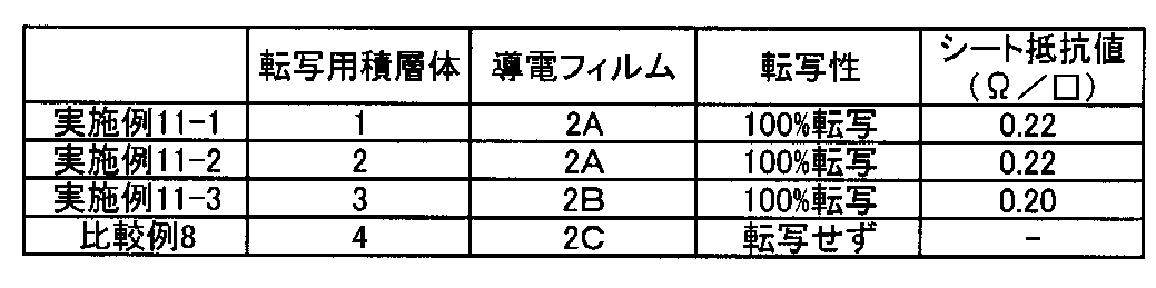
[実施例12-1~実施例12-3および比較例9]
転写用積層体1~4について、市販の上質紙に、転写用積層体の感圧接着剤塗布面がくるようにしてインクを取り除いたボールペンのペン先で押圧し、連続のパターンを描画した。その転写性を目視で確認し、パターンの両端をテスターで測定し、導通の有無を調べた。結果を表3に示す。
転写用積層体1~4について、市販の上質紙に、転写用積層体の感圧接着剤塗布面がくるようにしてインクを取り除いたボールペンのペン先で押圧し、連続のパターンを描画した。その転写性を目視で確認し、パターンの両端をテスターで測定し、導通の有無を調べた。結果を表3に示す。
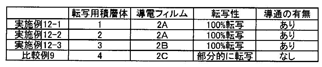
比較例9においては、転写用積層体4における導電層が部分的に被転写基材である上質紙上に転写されたが、転写用積層体4における導電層を上質紙上に転写することができなかった。
[実施例13-1~実施例13-3]
転写用積層体1~3について、市販の厚紙を箱状に組み立てたパッケージに対し、パッケージ表面に、転写用積層体の感圧接着剤塗布面がくるようにして、インクを取り除いたボールペンのペン先で押圧し、パッケージ側面を1周するように、連続のパターンを描画した。パターンの両端をテスターで測定し、導通の有無を調べた。結果を表4に示す。
転写用積層体1~3について、市販の厚紙を箱状に組み立てたパッケージに対し、パッケージ表面に、転写用積層体の感圧接着剤塗布面がくるようにして、インクを取り除いたボールペンのペン先で押圧し、パッケージ側面を1周するように、連続のパターンを描画した。パターンの両端をテスターで測定し、導通の有無を調べた。結果を表4に示す。
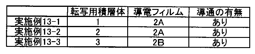
[実施例14]
実施例11-1における転写用積層体1を用いて、市販の上質紙に、転写用積層体1の感圧接着剤塗布面がくるようにして転写ヘッドで加圧し、第1多孔性導電層のラインパターンを転写した。更に、転写された第1多孔性導電層のラインパターンと交差するように、市販の上質紙に、転写用積層体の感圧接着剤塗布面がくるようにして転写ヘッドで加圧して第1多孔性導電層のラインパターンを転写した。図22に示すように、被転写基材11である上質紙上に第1多孔性導電層33、34のラインパターンが交差した転写物を作製した。それぞれの第1多孔性導電層33、34のラインパターンの端Y、Zにテスターをあてて調べたところ、2本の第1多孔性導電層33、34のラインパターンが導通していることを確認した。
実施例11-1における転写用積層体1を用いて、市販の上質紙に、転写用積層体1の感圧接着剤塗布面がくるようにして転写ヘッドで加圧し、第1多孔性導電層のラインパターンを転写した。更に、転写された第1多孔性導電層のラインパターンと交差するように、市販の上質紙に、転写用積層体の感圧接着剤塗布面がくるようにして転写ヘッドで加圧して第1多孔性導電層のラインパターンを転写した。図22に示すように、被転写基材11である上質紙上に第1多孔性導電層33、34のラインパターンが交差した転写物を作製した。それぞれの第1多孔性導電層33、34のラインパターンの端Y、Zにテスターをあてて調べたところ、2本の第1多孔性導電層33、34のラインパターンが導通していることを確認した。
[実施例15]
実施例11-2における転写用積層体2について、実施例14と同様に、図22に示す第1多孔性導電層33、34のラインパターンが交差した転写物を作製した。それぞれの第1多孔性導電層33、34のラインパターンの端Y、Zにテスターをあてて調べたところ、2本の第1多孔性導電層33、34のラインパターンが導通していないことを確認した。
更に、図22に示すように2本の第1多孔性導電層33、34のラインパターンの交点Xに対して、シリコーンゴム製の棒を用いて加圧した。加圧後の2本の第1多孔性導電層のラインパターンの端部Y、Zについてテスターをあてて調べたところ、2本の第1多孔性導電層33、34のラインパターンが導通していることを確認した。
実施例11-2における転写用積層体2について、実施例14と同様に、図22に示す第1多孔性導電層33、34のラインパターンが交差した転写物を作製した。それぞれの第1多孔性導電層33、34のラインパターンの端Y、Zにテスターをあてて調べたところ、2本の第1多孔性導電層33、34のラインパターンが導通していないことを確認した。
更に、図22に示すように2本の第1多孔性導電層33、34のラインパターンの交点Xに対して、シリコーンゴム製の棒を用いて加圧した。加圧後の2本の第1多孔性導電層のラインパターンの端部Y、Zについてテスターをあてて調べたところ、2本の第1多孔性導電層33、34のラインパターンが導通していることを確認した。
[実施例16]
導電フィルム2Aの上に、市販のテープのり2種(ドットライナープチ(ハート柄)、ドットライナープチ(スター柄)、コクヨS&T製)の粘着パターンを写し取り、転写用積層体とした。続いて、被転写基材として市販の上質紙に、上述の転写用積層体の粘着パターン面を重ね、樹脂製のヘラによって加圧したところ、パターン状(ハート型、星型)に銅膜を転写することができた。
導電フィルム2Aの上に、市販のテープのり2種(ドットライナープチ(ハート柄)、ドットライナープチ(スター柄)、コクヨS&T製)の粘着パターンを写し取り、転写用積層体とした。続いて、被転写基材として市販の上質紙に、上述の転写用積層体の粘着パターン面を重ね、樹脂製のヘラによって加圧したところ、パターン状(ハート型、星型)に銅膜を転写することができた。
[合成例3:銅粒子の合成]
200ml三ッ口フラスコ中に、水酸化銅 10.0g(和光純薬工業製)、デカン酸 34.5g(花王製ルナック10-98)、プロピレングリコールモノメチルエーテル(PGME)18.5gを量り取った。この混合液を撹拌しながら100℃まで加熱し、その温度を20分維持した。その後、3-エトキシプロピルアミン 41.3g(広栄化学工業製)を添加し、100℃で10分加熱、撹拌した。この混合液を、氷浴を用いて10℃まで冷却した後、氷浴中でヒドラジン一水和物 10.0gをPGME 18.5g(関東化学製)に溶解させた溶液を添加し、10分撹拌した。その後、反応溶液を100℃まで加熱し、その温度を10分維持した。30℃まで冷却後、ヘキサン66gを添加した。遠心分離後、上澄み液を除去した。沈殿物をヘキサンで洗浄し、銅粒子を得た。
得られた銅粒子を透過型電子顕微鏡(TEM)で観察したところ、平均一次粒径は65nmであった。
200ml三ッ口フラスコ中に、水酸化銅 10.0g(和光純薬工業製)、デカン酸 34.5g(花王製ルナック10-98)、プロピレングリコールモノメチルエーテル(PGME)18.5gを量り取った。この混合液を撹拌しながら100℃まで加熱し、その温度を20分維持した。その後、3-エトキシプロピルアミン 41.3g(広栄化学工業製)を添加し、100℃で10分加熱、撹拌した。この混合液を、氷浴を用いて10℃まで冷却した後、氷浴中でヒドラジン一水和物 10.0gをPGME 18.5g(関東化学製)に溶解させた溶液を添加し、10分撹拌した。その後、反応溶液を100℃まで加熱し、その温度を10分維持した。30℃まで冷却後、ヘキサン66gを添加した。遠心分離後、上澄み液を除去した。沈殿物をヘキサンで洗浄し、銅粒子を得た。
得られた銅粒子を透過型電子顕微鏡(TEM)で観察したところ、平均一次粒径は65nmであった。
[調製例3:銅粒子分散体の調製]
合成例1で得られた銅粒子40質量部、高分子分散剤としてソルスパース 41000(ルーブリゾール製)4質量部、プロピレングリコールモノメチルエーテル(PGME)56質量部を混合し、ペイントシェーカー(浅田鉄工製)にて予備分散として2mmジルコニアビーズで1時間、さらに本分散として0.1mmジルコニアビーズで2時間分散し、銅粒子分散体1を得た。
合成例1で得られた銅粒子40質量部、高分子分散剤としてソルスパース 41000(ルーブリゾール製)4質量部、プロピレングリコールモノメチルエーテル(PGME)56質量部を混合し、ペイントシェーカー(浅田鉄工製)にて予備分散として2mmジルコニアビーズで1時間、さらに本分散として0.1mmジルコニアビーズで2時間分散し、銅粒子分散体1を得た。
[製造例8:導電フィルム3Aの作製]
PETフィルム(商品名 コスモシャイン A4100、東洋紡製、膜厚100μm)に銅粒子分散体1をミヤバー#4を使って塗布し、温風乾燥機で80℃、3分乾燥させ、赤銅光沢を持つフィルムを得た。その後、水素ガスを導入圧力20Paで導入しながら、マイクロ波表面波プラズマ処理装置(MSP-1500、ミクロ電子株式会社製)を用いて、マイクロ波出力450Wで240秒間焼成し、導電層として多孔性導電層を有する導電フィルム3Aを得た。
PETフィルム(商品名 コスモシャイン A4100、東洋紡製、膜厚100μm)に銅粒子分散体1をミヤバー#4を使って塗布し、温風乾燥機で80℃、3分乾燥させ、赤銅光沢を持つフィルムを得た。その後、水素ガスを導入圧力20Paで導入しながら、マイクロ波表面波プラズマ処理装置(MSP-1500、ミクロ電子株式会社製)を用いて、マイクロ波出力450Wで240秒間焼成し、導電層として多孔性導電層を有する導電フィルム3Aを得た。
[製造例9:導電フィルム3Bの作製]
PETフィルム(商品名 コスモシャイン A4100、東洋紡製、膜厚100μm)に銅をスパッタ法により製膜し、導電層として蒸着導電層を有する導電フィルム3Bを得た。
PETフィルム(商品名 コスモシャイン A4100、東洋紡製、膜厚100μm)に銅をスパッタ法により製膜し、導電層として蒸着導電層を有する導電フィルム3Bを得た。
[導電フィルムの評価]
(導電層のシート抵抗値の測定)
導電層の導電性評価は、表面抵抗計(ダイアインスツルメンツ社製「ロレスタGP」、PSPタイププローブ)を用いて、4探針法によりシート抵抗値を測定することにより行った。導電フィルム3Aの多孔性導電層のシート抵抗値は0.20Ω/□であり、導電フィルム3Bの蒸着導電層のシート抵抗値は0.075Ω/□であった。
(導電層のシート抵抗値の測定)
導電層の導電性評価は、表面抵抗計(ダイアインスツルメンツ社製「ロレスタGP」、PSPタイププローブ)を用いて、4探針法によりシート抵抗値を測定することにより行った。導電フィルム3Aの多孔性導電層のシート抵抗値は0.20Ω/□であり、導電フィルム3Bの蒸着導電層のシート抵抗値は0.075Ω/□であった。
(導電層の膜厚の測定)
導電層の膜厚評価は下記の通り行った。作製した導電フィルムについて保護層として導電層上部に真空蒸着法にてカーボンを、スパッタ法にて白金を順次積層し、次いでFIB(集束イオンビーム、日立ハイテク製 FB-2100)を用いてタングステンを積層後、導電層の断面を作製した。その後、SEM(日立ハイテク製 S-4800)を用いて基板を45°傾斜させた状態にて導電層断面を観察し、SEM像より膜厚を測定した。膜厚は30k~40kの倍率で測定したSEM像内で10箇所測長し、傾斜分を補正した後、その平均値を膜厚とした。導電フィルム3Aおよび3Bの導電層の膜厚は400nmであった。この結果から導電フィルム3Aの体積抵抗値は8μΩ・cmであり、導電フィルム3Bの体積抵抗値は3μΩ・cmであることがわかった。
導電層の膜厚評価は下記の通り行った。作製した導電フィルムについて保護層として導電層上部に真空蒸着法にてカーボンを、スパッタ法にて白金を順次積層し、次いでFIB(集束イオンビーム、日立ハイテク製 FB-2100)を用いてタングステンを積層後、導電層の断面を作製した。その後、SEM(日立ハイテク製 S-4800)を用いて基板を45°傾斜させた状態にて導電層断面を観察し、SEM像より膜厚を測定した。膜厚は30k~40kの倍率で測定したSEM像内で10箇所測長し、傾斜分を補正した後、その平均値を膜厚とした。導電フィルム3Aおよび3Bの導電層の膜厚は400nmであった。この結果から導電フィルム3Aの体積抵抗値は8μΩ・cmであり、導電フィルム3Bの体積抵抗値は3μΩ・cmであることがわかった。
(導電層の空孔率の測定)
導電層の空孔率測定は下記の通り行った。上記膜厚測定において得られたSEM像における、孔の面積と導電層の面積とをそれぞれ算出し、孔の面積を導電層の面積で除することにより当該断面における空孔率を求めた。
より具体的には、上記測定は、上記「導電層の膜厚の測定」と同様の方法により30k~40kの倍率で撮影したSEM像を用いた。また、空孔率は、多孔性導電層の異なる10箇所で測定し、平均すること(各箇所での空孔率の合計を10で除すこと)により求めた。なお、各箇所での空孔率の測定はSEM像内の400nm×400nmの正方形断面内で行った。
その結果、導電フィルム3Aの多孔性導電層の空孔率は35%であった。また、導電フィルム3Bの導電層には空孔がなかった。
導電層の空孔率測定は下記の通り行った。上記膜厚測定において得られたSEM像における、孔の面積と導電層の面積とをそれぞれ算出し、孔の面積を導電層の面積で除することにより当該断面における空孔率を求めた。
より具体的には、上記測定は、上記「導電層の膜厚の測定」と同様の方法により30k~40kの倍率で撮影したSEM像を用いた。また、空孔率は、多孔性導電層の異なる10箇所で測定し、平均すること(各箇所での空孔率の合計を10で除すこと)により求めた。なお、各箇所での空孔率の測定はSEM像内の400nm×400nmの正方形断面内で行った。
その結果、導電フィルム3Aの多孔性導電層の空孔率は35%であった。また、導電フィルム3Bの導電層には空孔がなかった。
[実施例17]
接着剤である大日精化製 TM-R850(LV-NT)K3にメチルイソブチルケトン(MIBK)30重量%相当を追加し、十分撹拌することで塗布液を調整した。これを導フィルム3Aの銅箔面上にミヤバー#4で塗布、温風乾燥機で90℃、1分乾燥させて、第1多孔性導電層上に第1接着層が形成された導電基板Aを得た。
次にこの導電基板Aを20mm×100mmサイズに2枚切りだし、長辺の端部から20mmが重なるように接着層の形成面同士を重ね合わせ、日本GBC製マルチラミネーター GL835PROを使って、130℃、GAP1mm以下、搬送速度0.3m/minで加熱ラミネート処理により加熱圧着することで、積層配線板X-1を作製した。
接着剤である大日精化製 TM-R850(LV-NT)K3にメチルイソブチルケトン(MIBK)30重量%相当を追加し、十分撹拌することで塗布液を調整した。これを導フィルム3Aの銅箔面上にミヤバー#4で塗布、温風乾燥機で90℃、1分乾燥させて、第1多孔性導電層上に第1接着層が形成された導電基板Aを得た。
次にこの導電基板Aを20mm×100mmサイズに2枚切りだし、長辺の端部から20mmが重なるように接着層の形成面同士を重ね合わせ、日本GBC製マルチラミネーター GL835PROを使って、130℃、GAP1mm以下、搬送速度0.3m/minで加熱ラミネート処理により加熱圧着することで、積層配線板X-1を作製した。
[実施例18]
実施例17同様の塗布液を導電フィルム3Aの多孔性導電層上にアプリケーターを用いてWet膜厚で約254μmになるように塗布し、温風乾燥機で90℃、1分乾燥させ、導電基板Bを得た。これを20mm×100mmサイズに切り出した。
次に、被転写基材としてポリカーボネート(以下、PCと略す)およびポリメチルメタクリレート(以下、PMMAと略す)の積層フィルム C001(住友化学製 膜厚125μm)のPC面と導電基板Bの接着剤塗布面とを重ね、実施例17同様に加熱ラミネート処理を行った。その後、PETフィルムを剥離し、導電基板B2を得た。
多孔性導電層は被転写基材へ100%転写し、転写後の導電基板B2のシート抵抗値は0.22Ω/□であった。
次いで20mm×100mmサイズに切り出した導電基板AとB2の長辺の端部から20mmが重なるように接着層の形成面同士を重ね合わせ、さらに実施例17同様の加熱ラミネート処理により加熱圧着することで、積層配線板X-2を作製した。
実施例17同様の塗布液を導電フィルム3Aの多孔性導電層上にアプリケーターを用いてWet膜厚で約254μmになるように塗布し、温風乾燥機で90℃、1分乾燥させ、導電基板Bを得た。これを20mm×100mmサイズに切り出した。
次に、被転写基材としてポリカーボネート(以下、PCと略す)およびポリメチルメタクリレート(以下、PMMAと略す)の積層フィルム C001(住友化学製 膜厚125μm)のPC面と導電基板Bの接着剤塗布面とを重ね、実施例17同様に加熱ラミネート処理を行った。その後、PETフィルムを剥離し、導電基板B2を得た。
多孔性導電層は被転写基材へ100%転写し、転写後の導電基板B2のシート抵抗値は0.22Ω/□であった。
次いで20mm×100mmサイズに切り出した導電基板AとB2の長辺の端部から20mmが重なるように接着層の形成面同士を重ね合わせ、さらに実施例17同様の加熱ラミネート処理により加熱圧着することで、積層配線板X-2を作製した。
[比較例10]
導電フィルム3Aに代わり、導電フィルム3Bを用いた以外は、実施例17と同様の手順で積層配線板X-3を作製した。
導電フィルム3Aに代わり、導電フィルム3Bを用いた以外は、実施例17と同様の手順で積層配線板X-3を作製した。
[比較例11]
ミヤバー#8に変更した以外は、実施例17と同様の手順で積層配線板X-4を作製した。
ミヤバー#8に変更した以外は、実施例17と同様の手順で積層配線板X-4を作製した。
[積層配線板の評価]
実施例および比較例で作製された積層配線板X-1~X-4について、接着層上からの導通の確認、接着層除去後の導通の確認、および接着層の導電層上の膜厚を測定した。
実施例および比較例で作製された積層配線板X-1~X-4について、接着層上からの導通の確認、接着層除去後の導通の確認、および接着層の導電層上の膜厚を測定した。
(接着層上からの導通の確認)
実施例および比較例の積層配線板を構成する2つの導電基板のそれぞれ積層配線板X-1~X-4の端部から5mm程度の箇所での接着層側にテスターをあてることにより導通の確認を行った。
その結果、実施例および比較例の積層配線板X-1~X-4のいずれにおいても導通は確認できなかった。
実施例および比較例の積層配線板を構成する2つの導電基板のそれぞれ積層配線板X-1~X-4の端部から5mm程度の箇所での接着層側にテスターをあてることにより導通の確認を行った。
その結果、実施例および比較例の積層配線板X-1~X-4のいずれにおいても導通は確認できなかった。
(接着層除去後の導通の確認)
実施例および比較例の積層配線板X-1~X-4の積層配線板を構成する2つの導電基板のそれぞれの端部近傍(端部から5mm程度までの領域)の接着層をアセトンを使って除去し、図23に示すように、導電層3(3aおよび3b)の露出箇所19を形成し、2つの導電基板のそれぞれの露出箇所の導電層に対してテスターをあてることにより導通の確認を行った。
その結果、実施例17および実施例18のX-1およびX-2では、導通が確認された。
一方、比較例10および比較例11のX-3およびX-4では、導通が確認できなかった。
実施例および比較例の積層配線板X-1~X-4の積層配線板を構成する2つの導電基板のそれぞれの端部近傍(端部から5mm程度までの領域)の接着層をアセトンを使って除去し、図23に示すように、導電層3(3aおよび3b)の露出箇所19を形成し、2つの導電基板のそれぞれの露出箇所の導電層に対してテスターをあてることにより導通の確認を行った。
その結果、実施例17および実施例18のX-1およびX-2では、導通が確認された。
一方、比較例10および比較例11のX-3およびX-4では、導通が確認できなかった。
(接着層の膜厚の測定)
実施例17および比較例11について、接着層除去後の導通の確認の際に、接着層を除去した箇所と未除去箇所の膜厚の差から、導電層表面上の接着層の膜厚を確認した。
その結果、実施例17および比較例11の積層配線板の導電層上の接着層の膜厚は、それぞれ、4μmおよび8μmであった。
実施例17および比較例11について、接着層除去後の導通の確認の際に、接着層を除去した箇所と未除去箇所の膜厚の差から、導電層表面上の接着層の膜厚を確認した。
その結果、実施例17および比較例11の積層配線板の導電層上の接着層の膜厚は、それぞれ、4μmおよび8μmであった。
1 … 積層体
2a、2b、2c … 第1基材、第2基材、第3基材
3a、3b、3c … 第1多孔性導電層、第2多孔性導電層、第3多孔性導電層
4a、4b、4c … 第1接着層、第2接着層、第3接着層
6 … 保護層
10 … 導電性基材
11 … 被転写基材
2a、2b、2c … 第1基材、第2基材、第3基材
3a、3b、3c … 第1多孔性導電層、第2多孔性導電層、第3多孔性導電層
4a、4b、4c … 第1接着層、第2接着層、第3接着層
6 … 保護層
10 … 導電性基材
11 … 被転写基材
Claims (21)
- 第1基材と、前記第1基材の一方の面上の第1多孔性導電層と、前記第1多孔性導電層の前記第1基材とは反対側の面上の第1接着層とが積層された第1導電基板
を有する積層体。 - 前記第1基材が樹脂基材である請求の範囲第1に記載の積層体。
- 前記第1基材と前記第1多孔性導電層との間に第1保護層を有する請求の範囲第1項または第2項に記載の積層体。
- 前記第1接着層が第1感圧接着層である請求の範囲第1項に記載の積層体。
- 前記第1基材が樹脂基材である請求の範囲第4項に記載の積層体。
- 前記第1多孔性導電層が、金属を含有する請求の範囲第4項または第5項に記載の積層体。
- 前記第1基材と前記第1多孔性導電層との間に第1保護層を有する請求の範囲第4項から第6項までのいずれかに記載の積層体。
- 前記積層体の形態が帯状である請求の範囲第4項から第7項までのいずれかに記載の積層体。
- 第2基材と、前記第2基材の一方の面上の第2多孔性導電層と、前記第2多孔性導電層の前記第2基材とは反対側の面上の第2接着層とが積層された第2導電基板を有し、
前記第1導電基板および前記第2導電基板は、前記第1導電基板の前記第1接着層側の表面および前記第2導電基板の前記第2接着層側の表面が対向して配置された接合部を有し、
前記接合部では、前記第1導電基板と前記第2導電基板とが固着されており、かつ前記第1多孔性導電層と前記第2多孔性導電層とが電気的に接続されている請求の範囲第1項に記載の積層体。 - 第3基材と、前記第3基材の一方の面上の第3接着層と、前記第3接着層の前記第3基材とは反対側の面上の第3多孔性導電層と、を有する第3導電基板を有し、
前記第1導電基板および前記第3導電基板は、前記第1導電基板の前記第1接着層側の表面および前記第3導電基板の前記第3多孔性導電層側の表面が対向して配置された接合部を有し、
前記接合部では、前記第1導電基板と前記第3導電基板とが固着されており、かつ前記第1多孔性導電層と前記第3多孔性導電層とが電気的に接続されている請求の範囲第1項に記載の積層体。 - 前記接合部が、前記第1導電基板および前記第2導電基板のそれぞれの端部、または前記第1導電基板および前記第3導電基板のそれぞれの端部に形成されている請求の範囲第9項または第10項に記載の積層体。
- 前記第1多孔性導電層、前記第2多孔性導電層および前記第3多孔性導電層は、それぞれパターン状であり、さらに、前記第1多孔性導電層、前記第2多孔性導電層および前記第3多孔性導電層のそれぞれの前記接合部に相当する部位には、接続端子部を有する請求の範囲第9項から第11項のいずれかに記載の積層体。
- 前記第1多孔性導電層、前記第2多孔性導電層および前記第3多孔性導電層の空孔率がそれぞれ5%以上50%以下の範囲内であり、
前記第1接着層、前記第2接着層および前記第3接着層に含まれる接着材料が、それぞれ熱可塑性樹脂、熱硬化性樹脂、または光照射により粘着性または接着性が低下する感光性樹脂である請求の範囲第9項から第13項のいずれかに記載の積層体。 - 請求の範囲第1項から第3項までのいずれかに記載の積層体を準備する準備工程と、
被転写基材上に前記積層体の第1接着層および第1多孔性導電層を転写する転写工程と
を有する導電性基材の製造方法。 - 前記転写工程では、前記被転写基材上に前記積層体の第1接着層および前記第1多孔性導電層のパターンを転写する請求の範囲第14項に記載の導電性基材の製造方法。
- 請求の範囲第1項から第3項までのいずれかに記載の積層体を準備する準備工程と、
前記積層体を成形型に配置し、前記成形型内に被転写基材用溶融樹脂を射出し、固化させて、被転写基材を成形すると同時に、前記被転写基材に前記積層体を転写する成形および転写工程と、
前記積層体の第1基材を剥離する剥離工程と
を有する導電性基材の製造方法。 - 請求の範囲第4項から第8項までのいずれかに記載の積層体を準備する準備工程と、
被転写基材上に前記積層体の第1感圧接着層および第1多孔性導電層を加圧して転写する転写工程と
を有する導電性基材の製造方法。 - 前記転写工程では、帯状の前記積層体を用いて前記被転写基材上に前記第1感圧接着層および前記第1多孔性導電層のパターンを加圧して転写する請求の範囲第17項に記載の導電性基材の製造方法。
- 前記転写工程では、前記積層体の前記感圧接着層および前記第1多孔性導電層を前記被転写基材上に加圧して転写することにより、前記第1感圧接着層および前記第1多孔性導電層ならびに第2感圧接着層および第2多孔性導電層が積層された積層部を形成し、
さらに、前記積層部に対して加熱処理および加圧処理の少なくともいずれかの処理をすることにより、前記第1多孔性導電層および前記第2多孔性導電層を電気的に接続させる接続工程を有する請求の範囲第17項または第18項のいずれかに記載の導電性基材の製造方法。 - 請求の範囲第14項から第19項までのいずれかに記載の導電性基材の製造方法により、導電性基材を作製する導電性基材作製工程を有する電子デバイスの製造方法。
- 請求の範囲第8項に記載の積層体を用いて、被転写基材上に帯状の前記積層体の第1感圧接着層および第1多孔性導電層を加圧して転写するために用いられる転写具であって、
前記積層体と、
前記積層体の前記第1感圧接着層を外側にして巻き出す巻き出しリールと、
前記巻き出しリールから引き出された前記積層体の前記第1感圧接着層および前記第1多孔性導電層を前記被転写基材上に加圧して転写する転写ヘッドと、
前記第1感圧接着層および前記第1多孔性導電層の転写後の第1基材を巻き取る巻き取りリールと、
前記巻き出しリールおよび前記巻き取りリールを連動して回転させる連動機構と
を有する転写具。
Priority Applications (1)
| Application Number | Priority Date | Filing Date | Title |
|---|---|---|---|
| PCT/JP2016/063206 WO2017187558A1 (ja) | 2016-04-27 | 2016-04-27 | 積層体、それを用いた導電性基材の製造方法、電子デバイスの製造方法および転写具 |
Applications Claiming Priority (1)
| Application Number | Priority Date | Filing Date | Title |
|---|---|---|---|
| PCT/JP2016/063206 WO2017187558A1 (ja) | 2016-04-27 | 2016-04-27 | 積層体、それを用いた導電性基材の製造方法、電子デバイスの製造方法および転写具 |
Publications (1)
| Publication Number | Publication Date |
|---|---|
| WO2017187558A1 true WO2017187558A1 (ja) | 2017-11-02 |
Family
ID=60160310
Family Applications (1)
| Application Number | Title | Priority Date | Filing Date |
|---|---|---|---|
| PCT/JP2016/063206 Ceased WO2017187558A1 (ja) | 2016-04-27 | 2016-04-27 | 積層体、それを用いた導電性基材の製造方法、電子デバイスの製造方法および転写具 |
Country Status (1)
| Country | Link |
|---|---|
| WO (1) | WO2017187558A1 (ja) |
Cited By (1)
| Publication number | Priority date | Publication date | Assignee | Title |
|---|---|---|---|---|
| WO2025191174A1 (de) * | 2024-03-15 | 2025-09-18 | Tesa Se | Verfahren zur herstellung eines mehrlagigen empfängermaterials für den einsatz bei der verarbeitung von microled |
Citations (4)
| Publication number | Priority date | Publication date | Assignee | Title |
|---|---|---|---|---|
| JP2000031623A (ja) * | 1998-07-07 | 2000-01-28 | Nitto Denko Corp | 金属転写フィルムおよび電子部品の電極形成方法 |
| JP2007080822A (ja) * | 2006-09-11 | 2007-03-29 | Tdk Corp | 導電層を有する導電性フィルム及びその導電層が付与された物体 |
| JP2010182648A (ja) * | 2009-02-09 | 2010-08-19 | Toda Kogyo Corp | 透明導電性基板、色素増感型太陽電池用透明導電性基板及び透明導電性基板の製造方法 |
| JP2014099294A (ja) * | 2012-11-13 | 2014-05-29 | Toda Kogyo Corp | 基材の製造方法、基材、および基材を用いた成形体 |
-
2016
- 2016-04-27 WO PCT/JP2016/063206 patent/WO2017187558A1/ja not_active Ceased
Patent Citations (4)
| Publication number | Priority date | Publication date | Assignee | Title |
|---|---|---|---|---|
| JP2000031623A (ja) * | 1998-07-07 | 2000-01-28 | Nitto Denko Corp | 金属転写フィルムおよび電子部品の電極形成方法 |
| JP2007080822A (ja) * | 2006-09-11 | 2007-03-29 | Tdk Corp | 導電層を有する導電性フィルム及びその導電層が付与された物体 |
| JP2010182648A (ja) * | 2009-02-09 | 2010-08-19 | Toda Kogyo Corp | 透明導電性基板、色素増感型太陽電池用透明導電性基板及び透明導電性基板の製造方法 |
| JP2014099294A (ja) * | 2012-11-13 | 2014-05-29 | Toda Kogyo Corp | 基材の製造方法、基材、および基材を用いた成形体 |
Cited By (1)
| Publication number | Priority date | Publication date | Assignee | Title |
|---|---|---|---|---|
| WO2025191174A1 (de) * | 2024-03-15 | 2025-09-18 | Tesa Se | Verfahren zur herstellung eines mehrlagigen empfängermaterials für den einsatz bei der verarbeitung von microled |
Similar Documents
| Publication | Publication Date | Title |
|---|---|---|
| JP6849131B2 (ja) | 積層体、それを用いた導電性基材の製造方法、電子デバイスの製造方法、および転写具 | |
| Maekawa et al. | Drop-on-demand laser sintering with silver nanoparticles for electronics packaging | |
| ES2833274T3 (es) | Materiales de sinterización y métodos de fijación mediante el uso de los mismos | |
| US8984747B2 (en) | Method for manufacturing fabric type circuit board | |
| TWI356658B (en) | Members for circuit board, method and device for m | |
| KR20090121222A (ko) | 도전성 패턴의 형성 방법 및 그 형성 장치, 및 그 도전성 패턴을 갖는 기판 | |
| JP3248518U (ja) | 集積導電パターンをもつラベルを形成するための装置 | |
| JP6520133B2 (ja) | 積層体ならびにそれを用いた導電性基材の製造方法および電子デバイスの製造方法 | |
| CN104206030B (zh) | 用于在表面上产生导电图案的方法和装置 | |
| JP6710018B2 (ja) | 導電パターン基板の製造方法 | |
| TWI249475B (en) | Decorative pattern and its preparation | |
| JP6849130B2 (ja) | 積層体ならびにそれを用いた導電性基材の製造方法および電子デバイスの製造方法 | |
| JP6520143B2 (ja) | 積層体、それを用いた導電性基材の製造方法、電子デバイスの製造方法、および転写具 | |
| JP6699783B2 (ja) | 積層体ならびにそれを用いた導電性基材の製造方法および電子デバイスの製造方法 | |
| US20200242440A1 (en) | A method and an apparatus for producing a radio-frequency identification transponder | |
| WO2017187558A1 (ja) | 積層体、それを用いた導電性基材の製造方法、電子デバイスの製造方法および転写具 | |
| JP6699784B2 (ja) | 積層体、それを用いた導電性基材の製造方法、電子デバイスの製造方法、および転写具 | |
| JP2016139768A (ja) | 積層配線板 | |
| CN207560433U (zh) | 电磁波屏蔽膜及带电磁波屏蔽膜的印刷电路板 | |
| JP2020111679A (ja) | 両面粘着シート | |
| CN211509708U (zh) | 电磁波屏蔽膜及带电磁波屏蔽膜的印刷线路板 | |
| JP2019083347A (ja) | 導電パターン基板の製造方法 | |
| WO2018235590A1 (ja) | 配線基板の製造方法および導電性インク | |
| JP2016139746A (ja) | 積層配線基板 | |
| JP4571436B2 (ja) | 配線板の製造方法 |
Legal Events
| Date | Code | Title | Description |
|---|---|---|---|
| NENP | Non-entry into the national phase |
Ref country code: DE |
|
| 121 | Ep: the epo has been informed by wipo that ep was designated in this application |
Ref document number: 16900430 Country of ref document: EP Kind code of ref document: A1 |
|
| 122 | Ep: pct application non-entry in european phase |
Ref document number: 16900430 Country of ref document: EP Kind code of ref document: A1 |
|
| NENP | Non-entry into the national phase |
Ref country code: JP |