WO2017183610A1 - 巻線、コイル及びトランス - Google Patents
巻線、コイル及びトランス Download PDFInfo
- Publication number
- WO2017183610A1 WO2017183610A1 PCT/JP2017/015469 JP2017015469W WO2017183610A1 WO 2017183610 A1 WO2017183610 A1 WO 2017183610A1 JP 2017015469 W JP2017015469 W JP 2017015469W WO 2017183610 A1 WO2017183610 A1 WO 2017183610A1
- Authority
- WO
- WIPO (PCT)
- Prior art keywords
- winding
- wire
- layer
- coating layer
- strands
- Prior art date
Links
Images


Classifications
-
- H—ELECTRICITY
- H01—ELECTRIC ELEMENTS
- H01F—MAGNETS; INDUCTANCES; TRANSFORMERS; SELECTION OF MATERIALS FOR THEIR MAGNETIC PROPERTIES
- H01F5/00—Coils
-
- H—ELECTRICITY
- H01—ELECTRIC ELEMENTS
- H01F—MAGNETS; INDUCTANCES; TRANSFORMERS; SELECTION OF MATERIALS FOR THEIR MAGNETIC PROPERTIES
- H01F27/00—Details of transformers or inductances, in general
- H01F27/34—Special means for preventing or reducing unwanted electric or magnetic effects, e.g. no-load losses, reactive currents, harmonics, oscillations, leakage fields
-
- H—ELECTRICITY
- H01—ELECTRIC ELEMENTS
- H01B—CABLES; CONDUCTORS; INSULATORS; SELECTION OF MATERIALS FOR THEIR CONDUCTIVE, INSULATING OR DIELECTRIC PROPERTIES
- H01B13/00—Apparatus or processes specially adapted for manufacturing conductors or cables
- H01B13/06—Insulating conductors or cables
- H01B13/14—Insulating conductors or cables by extrusion
-
- H—ELECTRICITY
- H01—ELECTRIC ELEMENTS
- H01B—CABLES; CONDUCTORS; INSULATORS; SELECTION OF MATERIALS FOR THEIR CONDUCTIVE, INSULATING OR DIELECTRIC PROPERTIES
- H01B7/00—Insulated conductors or cables characterised by their form
-
- H—ELECTRICITY
- H01—ELECTRIC ELEMENTS
- H01B—CABLES; CONDUCTORS; INSULATORS; SELECTION OF MATERIALS FOR THEIR CONDUCTIVE, INSULATING OR DIELECTRIC PROPERTIES
- H01B7/00—Insulated conductors or cables characterised by their form
- H01B7/02—Disposition of insulation
-
- H—ELECTRICITY
- H01—ELECTRIC ELEMENTS
- H01B—CABLES; CONDUCTORS; INSULATORS; SELECTION OF MATERIALS FOR THEIR CONDUCTIVE, INSULATING OR DIELECTRIC PROPERTIES
- H01B7/00—Insulated conductors or cables characterised by their form
- H01B7/30—Insulated conductors or cables characterised by their form with arrangements for reducing conductor losses when carrying alternating current, e.g. due to skin effect
-
- H—ELECTRICITY
- H01—ELECTRIC ELEMENTS
- H01F—MAGNETS; INDUCTANCES; TRANSFORMERS; SELECTION OF MATERIALS FOR THEIR MAGNETIC PROPERTIES
- H01F27/00—Details of transformers or inductances, in general
- H01F27/28—Coils; Windings; Conductive connections
-
- H—ELECTRICITY
- H01—ELECTRIC ELEMENTS
- H01F—MAGNETS; INDUCTANCES; TRANSFORMERS; SELECTION OF MATERIALS FOR THEIR MAGNETIC PROPERTIES
- H01F27/00—Details of transformers or inductances, in general
- H01F27/28—Coils; Windings; Conductive connections
- H01F27/2823—Wires
-
- H—ELECTRICITY
- H01—ELECTRIC ELEMENTS
- H01F—MAGNETS; INDUCTANCES; TRANSFORMERS; SELECTION OF MATERIALS FOR THEIR MAGNETIC PROPERTIES
- H01F30/00—Fixed transformers not covered by group H01F19/00
- H01F30/06—Fixed transformers not covered by group H01F19/00 characterised by the structure
- H01F30/10—Single-phase transformers
-
- H—ELECTRICITY
- H01—ELECTRIC ELEMENTS
- H01F—MAGNETS; INDUCTANCES; TRANSFORMERS; SELECTION OF MATERIALS FOR THEIR MAGNETIC PROPERTIES
- H01F5/00—Coils
- H01F5/06—Insulation of windings
Definitions
- the present invention relates to a winding, a coil and a transformer.
- a switching power supply having a switching element and a transformer (also referred to as a transformer) is generally used.
- the commercial power supply is 50 Hz / 60 Hz.
- the size of the commercial power supply was reduced to a practical size by increasing the frequency of power transmission per second by increasing the frequency of the commercial power supply to several tens kHz or more using a switching element before transforming with a transformer.
- Switching power supplies are universally used.
- the transformer mounted on the switching power supply has a large coil loss when transforming high frequency AC voltage.
- the winding used for the high frequency transformer is required to have a low AC resistance at the time of applying a high frequency current as a coil, and a performance capable of further reducing the loss of the coil or the transformer.
- the winding used for the high frequency transformer in order to reduce the loss, it is effective to make the wire diameter smaller and increase the number of wires.
- the wire diameter is reduced, the skin effect at the time of energization can be suppressed, and the number of wires to be twisted can be increased.
- there is a limit to reducing the diameter of the wire In addition, in the case of a wire diameter in which the proximity effect becomes more dominant than the skin effect with respect to the AC resistance, the AC resistance can not be sufficiently reduced even if the diameter is reduced.
- An object of the present invention is to provide a winding having a small alternating current resistance at the time of energization of a high frequency current and capable of effectively suppressing the loss of the coil or the transformer, and a coil and a transformer using the same.
- the present inventors are a stranded wire in which a stranded wire formed using a wire having a magnetic layer of a specific thickness on the outer periphery of a copper wire having a characteristic wire diameter is coated with a resin layer having a thickness of 40 to 400 ⁇ m. It has been found that the alternating current resistance is sufficiently small when high frequency current is applied, and furthermore, when this coated stranded wire is used as a coil winding, it is possible to effectively suppress the loss of the coil or the transformer. The present inventors have further researched on the basis of this finding and made the present invention.
- the object of the present invention is achieved by the following means.
- the winding as described in ⁇ 1> which has a baking coating layer on the outer periphery of the ⁇ 2> above-mentioned magnetic substance layer.
- ⁇ 4> The winding according to any one of ⁇ 1> to ⁇ 3>, wherein the extrusion coating layer is composed of three or more layers.
- ⁇ 5> A coil using the winding according to any one of the above ⁇ 1> to ⁇ 4>.
- ⁇ 7> The transformer according to ⁇ 6>, which is for a high frequency switching power supply of 100 k to 1 MHz.
- a numerical range represented using “to” means a range including numerical values described before and after “to” as the lower limit value and the upper limit value.
- the present invention can provide a winding having a small alternating current resistance at the time of energization of a high frequency current and capable of effectively suppressing these losses when used for a coil or a transformer, and a coil and a transformer using the same.
- FIG. 1 is a schematic end view showing a preferred example of the winding of the present invention.
- FIG. 2 is a schematic end view showing a preferred example of the winding of the present invention.
- FIG. 3 is a schematic end view showing a preferred example of the winding of the present invention.
- FIG. 4 is a schematic end view showing a preferred example of the winding of the present invention.
- FIG. 5 is a schematic end view showing a preferred example of the winding of the present invention.
- FIG. 6 is a schematic end view showing a preferred example of the winding of the present invention.
- FIG. 7 is a schematic end view showing an example of a conventional winding.
- FIG. 8 is a graph showing the results of measuring the AC resistance value of each winding in the example.
- the winding of the present invention is preferably used as a winding of a coil or a transformer, and is a stranded wire formed by twisting a plurality of strands having a copper wire diameter of 0.05 to 0.5 mm, and the above plurality of strands. And an extrusion coating layer covering the In the winding of the present invention, at least one of the strands is a magnetic strand having a magnetic layer on the outer periphery of the copper wire. In addition, the thickness of the extrusion coating layer is 40 to 400 ⁇ m.
- the winding of the present invention having the above configuration can effectively suppress the AC resistance at the time of energization of a high frequency current.
- the extrusion coating layer can coat a plurality of strands
- the coating mode and the like of the strands are not particularly limited.
- the extrusion coating layer is preferably formed by extrusion molding because it has a thickness described later.
- this covering layer is referred to as an extrusion covering layer for convenience to distinguish it from the baking covering layer described later, but it is preferable if it can be distinguished from the baking covering layer generally provided on the copper wire side (inner side). It can also be referred to as an outer covering layer or an outer resin layer.
- the baked coating layer can also be referred to as an inner coating layer or an inner resin layer.
- the extrusion coated layer and the baked coating layer are not limited to the layers formed by extrusion molding or baking without being limited to their names, respectively, and the scope of the present invention is not limited thereto.
- the terms "extrusion” and “baking” are not to be considered as invention specific matters which interpret the present invention in a limited manner.
- the extrusion coating layer covers a plurality of strands
- an embodiment in which the extrusion coating layer is provided on the outer surface of the stranded wire to coat a plurality of strands (integrally) (the extrusion coating layer of this aspect is wound
- an embodiment in which a wire extrusion coating layer) and an extrusion coating layer are provided as the outermost layer of each wire to cover a plurality of strands (separately) the extrusion coating layer of this embodiment is referred to as a wire extrusion coating layer
- the extrusion coating layer preferably includes a wire extrusion coating layer.
- the thickness of the extrusion coating layer is the total thickness of the above-mentioned winding extrusion coating layer and the strand extrusion coating layer of the strands disposed in the outermost row of the stranded wire.
- the thickness of the wire extrusion coating layer and the winding extrusion coating layer usually refers to the difference between the inner diameter and the outer diameter of each extrusion coating layer.
- the thickness of the winding extrusion covering layer is a radius r L of a virtual circumscribed circle circumscribed to a plurality of strands arranged in the outermost row of the stranded wire in a cross section perpendicular to the winding axis, and the winding
- the difference (r T -r L ) with the radius r T of the outer contour of the extrusion coating layer is referred to.
- the radius r T of the wound extrusion is the radius of the imaginary circumscribed circle circumscribed to the outer contour of the wound extrusion in the above-mentioned cross section.
- the above-mentioned strands disposed in the outermost row of the stranded wire mean strands located in the outermost row among the strands disposed adjacent to each other in the radial direction of the strand.
- each layer such as an extrusion covering layer (a wire extrusion covering layer or a winding extrusion covering layer) may be a single layer or plural layers of two or more layers.
- the number of layers in each layer is determined by observing the layers in cross section regardless of the types and contents of resins and additives forming the layers. Specifically, when observing a cross section of a certain layer at a magnification of 200 times, if the annual ring-shaped boundary can not be confirmed, the total number of certain layers is 1 and if the annual ring-shaped boundary can be confirmed, the number of layers Is (the number of boundaries + 1).
- the present invention is not limited thereto.
- the outline shape of the winding extrusion covering layer is illustrated in a ring shape, but in the winding of the present invention, the shape of the outer outline of the winding extrusion covering layer is not limited to the ring shape, and a stranded wire And the gap between the
- the contour shape is not limited to a circle, and may be, for example, an oval shape, a flat knurled shape (gear shape or wave shape), or the like.
- the structure of the winding of the present invention is not particularly limited as long as it has a stranded wire and an extrusion coating layer. First, the structure of the winding will be described, and the details of the stranded wire and the like will be described later.
- Each of the windings 1A to 1E shown in FIGS. 1 to 5 is an embodiment having only a winding extrusion covering layer as an extrusion covering layer.
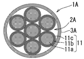
- a preferred winding 1A of the present invention has a stranded wire 2A formed by twisting seven magnetic baked coated strands 11 and an extruded covering layer 3A covering the outer periphery of the stranded wire 2A.
- a preferred winding 1B of the present invention has a stranded wire 2B formed by twisting 19 magnetic baked coated strands 11 and an extruded covering layer 3B covering the outer periphery of the stranded wire 2B. .
- the preferred winding 1C of the present invention is, as shown in FIG. 3, a stranded wire 2C formed by twisting 12 magnetic baked coated strands 11 and 7 baked coated strands 12 and a stranded wire 2C. And an extrusion covering layer 3C covering the outer periphery.
- the magnetic baked coated strands 11 are arranged on the outer periphery of the baked coated stranded wire 12.
- the magnetic baked sheathing wire 11 when the magnetic baked sheathing wire 11 is disposed on the outer periphery, it is possible to prevent the magnetic flux from the other adjacent windings from invading the inside of the winding, and the same number of the magnetic baked sheathed wire 11 (winding 1C In this case, the increase in AC resistance due to the proximity effect can be suppressed as compared with the winding having 19).
- the preferred winding 1D of the present invention is the same as the winding 1A except that the thickness of the extrusion covering layer 3D is different as shown in FIG.
- the preferred winding 1E of the present invention has a three-layer structure in which the extrusion coating layer 3E comprises the winding extrusion coating layers 3E 1 , 3E 2 and 3E 3 in order from the inside (twisted wire 2E). Except having it, it is the same as that of winding 1D.
- each layer forming the three-layer structure is set to the same thickness, but in the present invention, the relationship of the thickness of each layer is not particularly limited.
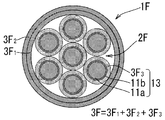
- the winding 1F is an aspect in which the extrusion coating layer 3F includes both the winding extrusion coating layers 3F 1 and 3F 2 and the wire-baking coating layer 3F 3 .
- the winding 1F includes a stranded wire 2F formed by twisting seven magnetic extrusion coated strands 13 having a strand extrusion coating layer 3F 3 as the outermost layer of the magnetic strands, and a winding covering the outer periphery of the stranded wire 2F. And an extrusion coating layer.
- This winding extrusion coating layer has a two-layer structure consisting of winding extrusion coating layers 3F 1 and 3F 2 sequentially from the inner side (strand 2F).
- the strands used for the windings 1A to 1F are not limited to the windings shown in the respective drawings, and may be changed to other strands not shown in each winding.
- the structures of the windings 1A to 1F may be combined appropriately.
- the stranded wire used in the present invention is not particularly limited as long as it is formed by twisting a plurality of strands including at least one strand having a magnetic layer on the outer periphery of a copper wire.
- the number of strands in stranding the strands can be, for example, 2 or more, and in consideration of the alignment of the strands, 7 or more in which 6 are disposed around one is preferable, and alternating current In consideration of resistance and practical processability, 100 or less is preferable. In particular, in view of alignment, the number is more preferably 7 to 37.
- the strands having the magnetic material layer on the outer periphery of the copper wire, which are included in the stranded wire, are disposed in the outermost row and the penetration of the linkage flux from the outside is effective. It is preferable in that it can be prevented, or it is preferable that strands having a magnetic material layer on the outer periphery of a copper wire and other strands are alternately arranged in that the proximity effect between the strands can be effectively prevented. .
- the strands arranged in the outermost row are not limited to the strands arranged adjacent to each other in the radial direction of the stranded wire in the thickness of the extrusion covering layer, and are arranged at the outermost side of the stranded wire Say the bare wire.
- the magnetic baked coated strand 11A in FIG. 2 is not a strand disposed in the outermost row in the thickness of the extrusion coated layer, but a strand disposed in the outermost row in the placement of the strands and become.
- the number of strands having a magnetic layer on the outer periphery of the copper wire contained in the stranded wire is not particularly limited as long as it is one or more.
- the strands having the magnetic layer in the outermost row it is preferably 40% or more with respect to the number of strands in consideration of 37 twists (18 strands arranged in the outermost row) .
- it in consideration of 7-strand twist (6 strands arranged in the outermost row), it is preferably 85% or more.
- the upper limit thereof is preferably 100% or less with respect to the number of strands.
- the strands having a magnetic layer on the outer periphery of the copper wire include magnetic strands, magnetic baked coated strands, and a strand having a strand extrusion covering layer on the outer periphery thereof, which will be described later.
- stranded wires 2A to 2F shown in FIGS. 1 to 6 can be mentioned.
- Copper wire As a copper wire, what is conventionally used by winding for coils etc. can be used. Preferably, a copper wire or a copper wire made of low-oxygen copper or elemental copper having an oxygen content of 30 ppm or less (more preferably 20 ppm or less) can be mentioned.
- the cross-sectional shape of the copper wire may be circular or rectangular (flat rectangular shape), but a circular shape is preferable in terms of twistability.
- the outer diameter ⁇ (wire diameter) of the copper wire is 0.05 to 0.5 mm. In this wire diameter, generally, the proximity effect is dominant over the skin effect.
- the copper wire of the above-mentioned wire diameter can be used.
- the wire diameter is not particularly limited as long as it is within the above range, but for example, 0.1 to 0.4 mm is more preferable.
- the magnetic wire is a wire having a magnetic layer on the outer periphery of the above-mentioned copper wire.
- the magnetic layer is a layer made of a magnetic material, and is provided on the outer peripheral surface of the copper wire.
- the magnetic material may be any substance having ferromagnetism, for example, nickel, Ni alloy (for example, Ni-Fe alloy), iron, iron alloy (electromagnetic soft iron, silicon steel, etc.), permalloy alloy, ferrite compound (for example) Mn-Zn ferrite etc. are mentioned.
- the magnetic material those suitable for electroplating are preferable, and, for example, nickel, Ni alloy, iron or iron alloy is more preferable.
- the thickness of the magnetic layer is not particularly limited, but is preferably, for example, 1 to 10% of the outer diameter of the copper wire in terms of alternating current resistance.
- the magnetic layer can be formed, for example, by electroplating.
- the plating solution and the plating conditions are not particularly limited.
- the winding of the present invention in which the wire diameter of the copper wire and the thickness of the extrusion coating layer are set in a specific range, if the stranded wire contains a magnetic wire, as described later, in the vicinity of a coil Since the penetration of the magnetic flux into the existing other copper wire or winding can be suppressed, the generation of the eddy current can be suppressed. As a result, it is considered that the winding of the present invention can suppress the increase in direct current resistance and the increase in alternating current resistance due to the skin effect and the proximity effect in a well-balanced manner and can reduce the alternating current resistance.
- the baked coated wire is a wire having a baked coated layer on the outer periphery of the above-mentioned copper wire.
- the baked coating layer is preferably a layer containing a thermosetting resin (also referred to as an enamel layer) as a resin component, and is provided on the outer peripheral surface of the copper wire.
- thermosetting resin if it is a thermosetting resin normally used by an electric wire or winding, it can be used, without being restrict
- polyamide imide (PAI), polyimide (PI), polyether imide (PEI), polyester imide (PEsI), polyurethane (PU), polyester (PEst), polybenzimidazole, melamine resin or epoxy resin, etc. may be mentioned.
- polyamide imide, polyimide, polyether imide, polyester imide, polyurethane or polyester is preferable.
- the thermosetting resin may contain one or more kinds.
- the baked coating layer may contain various additives commonly used in electric wires or windings.
- the content of the additive is not particularly limited, but is preferably 5 parts by mass or less, and more preferably 3 parts by mass or less with respect to 100 parts by mass of the resin component.
- the thickness of the baked coating layer is not particularly limited, but is preferably 10 to 15 ⁇ m, for example, in terms of achieving insulation between the strands and the space factor of the conductor (copper wire).
- the baked coating layer can be formed by a known method.
- a method of applying and baking a varnish of a resin component such as a thermosetting resin on the outer periphery of a copper wire or the like is preferable.
- This varnish contains a resin component, a solvent, and, optionally, a curing agent for the resin component or various additives.
- the solvent is preferably an organic solvent, and one that can dissolve or disperse the resin component is appropriately selected.
- the method of applying the varnish can be selected from ordinary methods, and examples thereof include a method using a varnish coating die having an opening similar or substantially similar to the cross-sectional shape of the copper wire.
- the baking of the varnish is usually carried out in a baking furnace.
- the conditions at this time can not be uniquely determined according to the type of the resin component or the solvent and the like, but for example, conditions of a furnace temperature of 400 to 650 ° C. and a passage time of 10 to 90 seconds can be mentioned.
- Magnetic Baked Coated Wire is a magnetic bare wire having a baked coated layer, has a magnetic layer on the outer periphery of the above-mentioned copper wire, and further has a baked coated layer on the outer periphery of the magnetic layer. .
- the copper wire, the magnetic layer and the baked coating layer in the magnetic baked coated wire are as described above.
- a wire having a wire extrusion covering layer on the outer periphery This wire is a wire extrusion covering layer as the outermost layer on a wire such as the above-mentioned copper wire, magnetic wire, baked covering wire or magnetic baked covering wire It is possessed.
- the copper wire, the magnetic layer and the baked coating layer in this wire are as described above.
- the wire extrusion coating layer may be a layer containing a thermoplastic resin, which will be described later, as a resin component.
- the thickness of the wire extrusion coating layer of the wire is not particularly limited as long as the thickness of the extrusion coating layer described later is satisfied, but in the case of further having a wire extrusion coating layer, for example, 15 to 30 ⁇ m is preferable.
- the wire extrusion coating layer is preferably formed by extruding (extrusion coating) a resin composition described later on the outer periphery of a copper wire or the like.
- Extruded coating layer As long as the extrusion coating layer can coat a plurality of strands, its structure, formation position, and the like are not particularly limited.
- the formation position is as described in the above-mentioned coating mode.
- the thickness of the extrusion coating layer is 40 to 400 ⁇ m.
- the thickness of the extrusion coating layer is within the above range, as shown in the example, direct current resistance, skin effect and The balance with the resistance by the proximity effect can be balanced, and as a result, the AC resistance can be effectively suppressed.
- the space factor can be increased while suppressing the increase in the resistance due to the skin effect, so that the direct current resistance can be suppressed. Since the distance between the windings can not be sufficiently secured, it is not possible to sufficiently suppress the AC resistance due to the proximity effect.
- the finished outer diameter of the stranded wire must be the same.
- the thickness of the extrusion coating layer is 40 to 400 ⁇ m, in addition to the above effects, bending workability of the winding is good and it can be wound around a small core. It is possible to sufficiently meet the demand for smaller or lighter coils.
- the creeping distance between the windings when forming a coil can be sufficiently secured, the insulating tape between the primary coil and the secondary coil in the transformer and the insulating tape between the coil and the core can be omitted, and the transformer It is effective for further miniaturization of
- the thickness of the extrusion coating layer is preferably 40 to 200 ⁇ m, and more preferably 60 to 100 ⁇ m from the viewpoint of reduction of AC resistance and further reduction in size or weight.
- the extrusion coating layer may have a laminate structure of two or more layers as described above, and among them, the wire extrusion coating layer preferably has a laminate structure of 3 layers or more, more preferably 3 to 5 layers. Can.
- the laminated structure has three or more layers, a sufficient creeping distance of the winding can be secured, and therefore, in the transformer of the present invention, the insulating tape which is usually used to secure the insulation can be omitted.
- the thickness of each layer is not particularly limited as long as the total thickness of each layer is in the above range. For example, in the case of having an inner layer, an intermediate layer and an outer layer, the thickness of each layer is preferably 13 to 130 ⁇ m.
- the extrusion coating layer preferably contains a thermoplastic resin as a resin component.
- the thermoplastic resin can be used without particular limitation as long as it is a thermoplastic resin generally used for electric wires or windings.
- polyamide polyamide
- polyacetal POM
- polycarbonate PC
- PPE polyphenylene ether
- PBT polyethylene terephthalate
- PET polyethylene naphthalate
- PEN polyethylene naphthalate
- super Other than general purpose engineering plastics such as high molecular weight polyethylene, polysulfone (PSF), polyethersulfone (PES), polyphenylene sulfide (PPS), polyarylate (PAR), polyetherketone (PEK), polyaryletherketone (PAEK), Tetrafluoroethylene / ethylene copolymer (ETFE), polyetheretherketone (PEEK, including modified PEEK), polyetherketoneketone (PEKK)
- Super engineering plastics such as te
- the resin components contained at the maximum content in each layer may be the same as or different from each other.
- the extrusion coating layer may contain various additives commonly used in electric wires or windings.
- the content of the additive is not particularly limited, but is preferably 5 parts by mass or less, and more preferably 3 parts by mass or less with respect to 100 parts by mass of the resin component.
- the extrusion coating layer has the thickness described above, it can be formed by extruding (extrusion coating) the resin composition on the outer periphery of the stranded wire.
- the resin composition contains the above-mentioned resin component and, if necessary, various additives.
- the extrusion method can not be determined uniquely depending on the type of resin component etc. However, for example, using an extrusion die having an opening similar or nearly similar to the cross-sectional shape of a copper wire etc.
- the method of extruding at the temperature of The extrusion coating layer is preferably formed by extrusion molding, but is not limited to this, and using the varnish containing the above-mentioned thermoplastic resin, solvent and the like, and various additives as necessary, the above-mentioned baked coating layer and It can also be formed in the same manner. From the viewpoint of productivity, it is preferable to form an extrusion coated layer by extrusion.
- the winding of the present invention has a stranded wire obtained by twisting a plurality of small diameter strands having a copper wire diameter of 0.05 to 0.5 mm.
- the stranded wire includes at least one magnetic strand.
- the winding according to the invention has an extruded covering of a certain thickness.
- the coil of the present invention uses the winding of the present invention described above. Specifically, an iron core made of a ferromagnetic or ferrimagnetic material or air is used as a core around which the winding of the present invention is wound.
- the size of the core such as the iron core is appropriately selected according to the application and the like.
- the winding method, the number of turns (two or more), the pitch and the like may be appropriately selected according to the application and the like.
- the winding of the present invention can effectively suppress the rise in AC resistance due to the increase in frequency as described above, it is possible to reduce the number of wires used to perform a predetermined transformer function. Alternatively, since the operating frequency of the transformer can be increased, the core size can be reduced by that amount, or the number of turns can be reduced.
- the transformer of the present invention has the coil of the present invention, its structure or size is not particularly limited.
- a plurality of coils including a coil on the input side (primary coil) and a coil on the output side (secondary coil) are provided.
- the transformer can convert an alternating voltage according to the turns ratio of the primary coil and the secondary coil.
- the transformer of the present invention comprises two or more, preferably two, coils, at least one of which comprises the coil of the present invention. More preferably, both are coils of the present invention.
- the transformer of the present invention may have a primary coil and a secondary coil in which windings are wound around different cores, and the windings of the primary coil may be wound directly or through an insulating tape or the like around the same core. And the winding of the secondary coil may be wound respectively.
- the coil and transformer of the present invention are preferably used for power supply, particularly for switching power supply.
- a power supply is a device that supplies a specific voltage and current.
- the coil and transformer of the present invention are preferably used as a switching power supply, and in particular, alternating current (AC) / direct current (DC) that transforms and rectifies alternating current commercial power and converts it into direct current of a voltage suitable for electric and electronic devices. It is preferably used for DC converter.
- the size can be reduced as the frequency is increased, but the AC resistance value of the winding and the loss of the switching element are increased, and the amount of heat generation is increased.
- the winding of the present invention can effectively suppress the AC resistance at the time of energization of a high frequency current when formed into a coil. Therefore, the loss of the coil or transformer using the winding of the present invention can be effectively suppressed. Further, the heat generation due to the resistance of the coil is suppressed, and the temperature rise of the coil is reduced, which contributes to further downsizing of the coil and the like. Furthermore, the frequency applicable to the transformer (switching power supply) can be further increased.
- the frequency applicable to the transformer of the present invention is not particularly limited, and examples thereof include 100 k to 1 MHz.
- the alternating current resistance generally decreases as the number of strands in the stranded wire increases, the outer diameter of the winding increases.
- the winding of the present invention can reduce the alternating current resistance as described above, it is possible to reduce the number of strands in the stranded wire used to achieve a predetermined transformer function. Therefore, the increase in the outer diameter of the winding can be suppressed, and the bending workability at the time of winding around a core or the like is also excellent.
- use of the insulating tape etc. which are used between a coil and a core, for example can be abbreviate
- the transformer of the present invention has the coil of the present invention. Therefore, in addition to the above-mentioned effects, the electric transmission efficiency is further increased, and the temperature rise can be suppressed, so that the effect of reducing the number of heat countermeasure components such as the cooling fan and the heat sink can be achieved.
- Example 1 the winding 1E shown in FIG. 5 (however, the extrusion covering layer has a two-layer structure) was manufactured as follows. (Production of winding) -Preparation of magnetic baked coated wire- First, seven magnetic baked coated strands 11 were produced. That is, iron was electroplated on the surface of a copper wire (circular cross section) 11a having a wire diameter of 0.12 mm to form a magnetic layer 11b having a thickness of 2.0 ⁇ m. Next, a polyurethane resin varnish (trade name: TPU F2-NC, manufactured by Toko Paint Co., Ltd.) is applied and baked onto the surface of the magnetic layer 11b, and this is repeated several times to form a baked coating layer 11c having a thickness of 10 ⁇ m.
- TPU F2-NC a polyurethane resin varnish
- This extrusion is repeated twice, and a winding 1E (outside diameter 0.564 mm) having a twisted wire 2E and a two-layered extrusion covering layer 3E consisting of a winding extruding covering layer 3E 1 and 3E 2 with a thickness of 66 ⁇ m Manufactured.
- the coil 1E of Example 1 was manufactured by winding the thus obtained winding 1E on a bobbin with an outer diameter of 15 mm for 36 turns. In this coil, the wound windings were in contact with each other.
- Example 2 In the formation of the extrusion coating layer of Example 1, a stranded wire 2E and an extrusion coating layer 3E having a thickness of 99 ⁇ m are prepared in the same manner as in the production of the winding of Example 1, except that the extrusion molding is repeated three times. Winding 1E (outer diameter 0.630 mm) which it has was manufactured. The extrusion coating layer 3E has a three-layer structure consisting of winding the extruded covering layer 3E 1 ⁇ 3E 3. Moreover, the coil of Example 2 was manufactured similarly to Example 1 using the obtained winding.
- Comparative Example 1 In the manufacture of the winding of Example 1, in the same manner as the manufacture of the winding of Example 1 except that the above-mentioned extrusion was not performed, a stranded wire 2E not having an extrusion covering layer (a thickness of 0 ⁇ m of the extrusion covering layer , Outer diameter 0.432 mm). Further, a coil of Comparative Example 1 was manufactured in the same manner as Example 1 using the obtained winding.
- Comparative Example 2 In the formation of the extrusion coating layer of Example 1, except that the extrusion molding was performed once, in the same manner as the production of the winding of Example 1, a stranded wire 2E and an extrusion coating layer with a thickness of 33 ⁇ m (monolayer And an outer diameter of 0.498 mm). Further, using the obtained winding, a coil of Comparative Example 2 was manufactured in the same manner as Example 1.
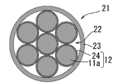
- a winding 21 (FIG. 7) having a stranded wire 22 composed of seven baked coated strands 12 and an extruded coated layer 23 was manufactured as follows.
- the winding is carried out in the same manner as the manufacture of the winding of Example 1, except that the magnetic layer 11b is not provided and the baked coated layer 24 having a thickness of 10 ⁇ m is formed.
- the thickness 66 ⁇ m of the extrusion coating layer 23 and the outer diameter 0.552 mm) 21 was produced.
- a coil of Comparative Example 3 was manufactured in the same manner as Example 1 using the obtained winding 21.
- Example 2 (a thickness of 99 ⁇ m of an extrusion covering layer), Comparative Example 1, except that the magnetic covering layer 11b was not provided and the baking covering layer 24 having a thickness of 10 ⁇ m was formed in the preparation of the magnetic sticking covering wire of Example 1.
- Windings 21 shown in FIG. 7 were produced analogously to the production of the windings 2 and 3 respectively.
- the thickness of the extrusion coating layer 23 is 99 ⁇ m, 0 ⁇ m and 33 ⁇ m, respectively, and the outer diameter is 0.618 mm, 0.420 mm and 0.486 mm, respectively. there were.
- the coils of Comparative Examples 4 to 6 were manufactured in the same manner as in Example 1 using the obtained windings 21 respectively.
- the reduction ratio with respect to the alternating current resistance value of Comparative Example 5 or 1 in which the thickness of the extrusion coating layer is 0 ⁇ m is 92% (Comparative Example 6), 86% (Comparative Example) 3), 84% (comparative example 4) and 68% (comparative example 2).
- the thickness of the extrusion coating layer was reduced to 55% in Example 1 having a thickness of 66 ⁇ m, and 53% in Example 2 having a thickness of 99 ⁇ m on the extrusion coating layer.
- the extrusion coating layer in order to reduce the alternating current resistance, it is effective to make the extrusion coating layer as thin as possible to increase the copper wire cross-sectional area, that is, to increase the space factor.
- the effect of the AC resistance increase due to the proximity effect is larger than that of the DC resistance. Therefore, it has been confirmed that it is more effective to increase the distance between the copper wires to reduce the increase in AC resistance due to the proximity effect than to increase the cross-sectional area of the copper wire to reduce the direct current resistance.
- the magnetic flux flowing into the magnetic layer 11b is consumed as heat energy, a part of it may generate an eddy current in the nearby copper wire 11a to increase the alternating current resistance value.
- the distance between the copper wires is properly secured, it is considered that the above-mentioned magnetic flux penetration and the generation of the eddy current can be prevented in a well-balanced manner.
- the magnetic flux between the windings is better than the prevention of the magnetic flux intrusion between the copper wires and the generation of the eddy current with respect to the reduction of the AC resistance. It is more effective to prevent intrusion and generation of eddy current.
- a winding of the present invention having a stranded wire 2E including a magnetic wire 11 coated with a magnetic wire and a copper wire having a specific wire diameter and an extruded covering layer 3E having a specific thickness on the outer periphery of the stranded wire 2E. It has been found that the wire 1E has a small alternating current resistance when a high frequency current is applied, and that the loss can be effectively suppressed when it is used for a coil or a transformer.
Landscapes
- Engineering & Computer Science (AREA)
- Power Engineering (AREA)
- Manufacturing & Machinery (AREA)
- Coils Of Transformers For General Uses (AREA)
- Insulated Conductors (AREA)
- Coils Or Transformers For Communication (AREA)
- Artificial Filaments (AREA)
Abstract
Description
スイッチング電源に搭載されるトランスは、高周波数の交流電圧を変圧する際には、コイルの損失が大きくなる。そのため、この損失を抑えることができるトランスが検討されている。例えば、複数の素線を撚り合わせた撚り線を巻回したコイルを備えたものが挙げられる。このようなコイルとして、例えば、特許文献1に記載のリッツ線コイルが挙げられる。
上述のコイルにおいて、損失を低減するには、素線径を細くし、素線数を増やすことが効果的である。素線径を細くすると、通電時の表皮効果を抑えられ、また撚り合わせる素線数を多くすることもできる。しかし、素線の細径化には限界がある。また、交流抵抗に対して表皮効果よりも近接効果が支配的になる線径においては、細径化しても、交流抵抗を十分に低減することはできない。
<1>銅線の線径が0.05~0.5mmの素線を複数本撚り合わせてなる撚り線と、前記複数の素線を被覆する押出被覆層とを有する巻線であって、
前記素線の少なくとも1本が前記銅線の外周に磁性体層を有し、
前記押出被覆層の厚みが40~400μmである、巻線。
<2>前記磁性体層の外周に焼付被覆層を有する<1>に記載の巻線。
<3>前記押出被覆層が、前記撚り線の外面に有する巻線押出被覆層を含む<1>又は<2>に記載の巻線。
<4>前記押出被覆層が、3層以上の層からなる<1>~<3>のいずれか1項に記載の巻線。
<5>上記<1>~<4>のいずれか1項に記載の巻線を用いたコイル。
<6>上記<5>に記載のコイルを有するトランス。
<7>100k~1MHzの高周波スイッチング電源用である<6>に記載のトランス。
本発明の上記及び他の特徴及び利点は、適宜添付の図面を参照して、下記の記載からより明らかになるであろう。
本発明の巻線は、コイル又はトランスの巻線として好ましく用いられ、銅線の線径が0.05~0.5mmの素線を複数本撚り合わせてなる撚り線と、上記複数の素線を被覆する押出被覆層とを有する。
本発明の巻線において、素線の少なくとも1本が銅線の外周に磁性体層を有する磁性素線である。また、押出被覆層の厚みが40~400μmである。
上記構成を有する本発明の巻線は、高周波電流の通電時の交流抵抗を効果的に抑えることができる。
押出被覆層が複数の素線を被覆する態様としては、押出被覆層が撚り線の外面に設けられて、複数の素線を(一体的に)被覆する態様(この態様の押出被覆層を巻線押出被覆層という)と、押出被覆層が各素線の最外層として設けられて、複数の素線を(別々に)被覆する態様(この態様の押出被覆層を素線押出被覆層という)と、これらを併用する態様を含む。いずれの態様においても、上記構成を有する巻線に上記厚みの押出被覆層を設けることにより、後述するように、近接効果による交流抵抗を効果的に低減できる。
本発明においては、押出被覆層は巻線押出被覆層を含むことが好ましい。
素線押出被覆層及び巻線押出被覆層の厚みは、通常、各押出被覆層の内径と外径との差分をいう。詳しくは、巻線押出被覆層の厚みは、巻線の軸線に垂直な断面において、撚り線の最外列に配置された複数の素線に外接する仮想外接円の半径rLと、巻線押出被覆層の外側輪郭線の半径rTとの差分(rT-rL)をいう。巻線押出被覆層の外側輪郭線が円形でない場合、巻線押出被覆層の半径rTは、上記断面において、巻線押出被覆層の外側輪郭線に外接する仮想外接円の半径とする。
ここで、上述の、撚り線の最外列に配置された素線とは、撚り線の半径方向に互いに隣接して配置された素線のうち最外列に位置する素線をいう。
本発明において、各層の層数は、層を形成する樹脂及び添加剤の種類及び含有量の異同にかかわらず、層を断面観察することによって、決定される。具体的には、ある層の断面を倍率200倍で観察したときに、年輪状の境界を確認できない場合、ある層の総数は1とし、年輪状の境界を確認できる場合、ある層の層数は(境界数+1)とする。
なお、各図において、巻線押出被覆層の輪郭形状を輪環状に図示したが、本発明の巻線においては、巻線押出被覆層の外側輪郭線の形状は輪環状に限らず、撚り線との間隙を充填していてもよい。この場合、輪郭形状は、円形に限定されず、例えば、楕円形、平目ローレット状(歯車形状もしくは波形状)等であってもよい。
本発明の巻線は、撚り線と押出被覆層とを有していれば、その構造は特に限定されない。まず、巻線の構造について説明し、撚り線等の詳細は後述する。
図1~図5に示される巻線1A~1Eは、いずれも、押出被覆層として巻線押出被覆層のみを有する態様である。
本発明の好ましい巻線1Aは、図1に示されるように、磁性焼付被覆素線11を7本撚り合わせてなる撚り線2Aと、撚り線2Aの外周を被覆する押出被覆層3Aとを有する。
本発明の好ましい巻線1Bは、図2に示されるように、磁性焼付被覆素線11を19本撚り合わせてなる撚り線2Bと、撚り線2Bの外周を被覆する押出被覆層3Bとを有する。
撚り線2Cにおいて、磁性焼付被覆素線11は、焼付被覆素線12の外周に配列されている。このように撚り線を磁性焼付被覆素線11と焼付被覆素線12とで形成すると、交流抵抗の低減とコストとのバランスを取ることができ、用途又は要求性能に応じた巻線とすることができる。また、磁性焼付被覆素線11が外周に配置されていると、隣接する他の巻線による磁束が巻線内部に侵入することを防止でき、磁性焼付被覆素線11を同数(巻線1Cの場合、19本)有する巻線に比べて、近接効果による交流抵抗の増大を抑えることができる。
本発明の好ましい巻線1Eは、図5に示されるように、押出被覆層3Eが、内側(撚り線2E)から順に巻線押出被覆層3E1、3E2及び3E3からなる3層構造を有していること以外は、巻線1Dと同様である。巻線1Eにおいて、3層構造を形成する各層は、いずれも、同一の厚みに設定されているが、本発明においては、各層の厚みの関係は特に限定されない。
また、本発明の巻線の構造として、上記巻線1A~1Fの各構造を適宜に組み合わせた構造とすることもできる。
本発明に用いる撚り線は、銅線の外周に磁性体層を有する素線を少なくとも1本含む複数の素線を撚り合わせてなるものであれば、特に限定されない。
素線を撚り合わせる際の、素線数としては、例えば、2本以上とすることができ、素線の整列性を考えると1本の周囲に6本を配置した7本以上が好ましく、交流抵抗と実用的な加工性を考えると100本以下が好ましい。特に整列性を考えると、より好ましくは7~37本である。
撚り線に含まれる、銅線の外周に磁性体層を有する素線の本数は、1本以上であれば特に限定されない。磁性体層を有する素線を最外列に配置する場合、37本撚り(最外列に配置される素線18本)を考慮すると、素線数に対して、好ましくは40%以上である。また、7本撚り(最外列に配置される素線6本)を考慮すると、好ましくは85%以上である。一方、その上限は、前記素線数に対して、100%以下が好ましい。
銅線の外周に磁性体層を有する素線としては、後述する、磁性素線、磁性焼付被覆素線及びこれらの外周に素線押出被覆層を有する素線を含む。
このような撚り線としては、例えば、図1~図6に示した撚り線2A~2F等が挙げられる。
撚り線を形成する素線としては、銅線、磁性素線、焼付被覆素線又は磁性焼付被覆素線等が挙げられる。また、これらの素線それぞれの外周に素線押出被覆層を有する素線等も挙げられる。
銅線としては、従来、コイル用等の巻線で用いられているものを使用することができる。好ましくは、銅線、又は、酸素含有量が30ppm以下(より好ましくは20ppm以下)の低酸素銅若しくは素銅からなる銅線が挙げられる。
銅線の断面形状は、円形でも矩形(平角形状)でもよいが、撚り性の点で、円形が好ましい。
銅線の外径φ(線径)は0.05~0.5mmである。この線径では、一般的に、表皮効果よりも近接効果が支配的になる。しかし、本発明においては、高周波電流の通電時の交流抵抗を十分に抑えることができるので、上記線径の銅線を用いることができる。線径は、上記範囲内であれば特に限定されないが、例えば、0.1~0.4mmがより好ましい。
磁性素線は、上述の銅線の外周に磁性体層を有する素線である。
この磁性体層は、磁性体材料からなる層であり、銅線の外周表面に設けられる。磁性体層を有する素線を用いることにより、コイルないしはトランスの損失を更に抑えることができる。
磁性体材料としては、強磁性を有する物質であればよく、例えば、ニッケル、Ni合金(例えば、Ni-Fe合金)、鉄、鉄合金(電磁軟鉄、ケイ素鋼等)、パーマロイ合金、フェライト化合物(Mn-Znフェライト等)が挙げられる。磁性体材料としては、電気めっきに適したものが好ましく、例えば、ニッケル、Ni合金、鉄又は鉄合金がより好ましい。
磁性体層の厚みは、特に限定されないが、交流抵抗の点で、例えば、銅線の外径の1~10%が好ましい。
磁性体層は、例えば、電気めっきで形成することができる。めっき液及びめっき条件は特に限定されない。
銅線の線径と押出被覆層の厚みとを特定の範囲に設定した本発明の巻線において、撚り線が磁性素線を含んでいると、後述するように、コイルとしたときに近傍に存在する他の銅線又は巻線への磁束の侵入を抑制できるため、渦電流の発生を抑制できる。その結果、本発明の巻線は、直流抵抗増大と、表皮効果及び近接効果による交流抵抗増大とをバランスよく抑制でき、交流抵抗の低減が可能になると、考えられる。
焼付被覆素線は、上述の銅線の外周に焼付被覆層を有する素線である。
この焼付被覆層は、樹脂成分として、好ましくは熱硬化性樹脂を含む層(エナメル層ともいう。)であり、銅線の外周表面に設けられる。
ワニスの塗布方法は、通常の方法を選択することができ、例えば、銅線の断面形状と相似形若しくは略相似形の開口を有するワニス塗布用ダイスを用いる方法等が挙げられる。ワニスの焼付けは、通常、焼付炉で行われる。このときの条件は、樹脂成分又は溶媒の種類等に応じて一義的に決定できないが、例えば、炉内温度400~650℃にて通過時間を10~90秒の条件が挙げられる。
磁性焼付被覆素線は、焼付被覆層を有する磁性素線であり、上述の銅線の外周に磁性体層を有し、更にこの磁性体層の外周に焼付被覆層を有する。
磁性焼付被覆素線における銅線、磁性体層及び焼付被覆層はそれぞれ上記の通りである。
この素線は、上述の、銅線、磁性素線、焼付被覆素線又は磁性焼付被覆素線等の素線に最外層として素線押出被覆層を有するものである。
この素線における、銅線、磁性体層及び焼付被覆層はそれぞれ上記の通りである。
素線押出被覆層は、樹脂成分として、好ましくは後述する熱可塑性樹脂を含有する層であればよい。素線の最外層として素線押出被覆層を設けることにより、下記押出被覆層と同様に、近接効果による交流抵抗を抑えることができる。
素線が有する素線押出被覆層の厚みは、後述する押出被覆層の厚みを満たす限り、特に限定されないが、巻線押出被覆層を更に有する場合、例えば15~30μmが好ましい。
素線押出被覆層は、銅線等の外周に、後述する樹脂組成物を押出成形(押出被覆)することにより、形成する方法が好ましい。
押出被覆層は、複数の素線を被覆することができれば、その構造及び形成位置等は特に限定されない。形成位置については、上記被覆態様において説明した通りである。
また、上記本発明の巻線は、押出被覆層の厚みが40~400μmであるので、上記効果に加えて、巻線の曲げ加工性が良く、サイズの小さな芯に巻くことでき、スイッチング電源又はコイルの小型化ないしは軽量化の要請に十分に応えることができる。更には、コイルとしたときの巻線間の沿面距離を十分に確保できるので、トランス中の一次コイルと二次コイル間の絶縁テープ、コイルと芯間の絶縁テープを省略することができ、トランスの更なる小型化に効果的である。
押出被覆層が積層構造を有する場合、各層の厚みは、各層の合計厚みが上記範囲内となれば特に限定されない。例えば、内側層、中間層及び外側層を有する場合、各層の厚みは13~130μmが好ましい。
熱可塑性樹脂は、1種又は2種以上含有していてもよい。
押出被覆層は、押出成形で形成することが好ましいが、これに限定されず、上述の熱可塑性樹脂と溶媒等と必要により各種の添加剤とを含有するワニスを用いて、上記焼付被覆層と同様にして、形成することもできる。
生産性の点で、押出成形により押出被覆層を形成することが好ましい。
<コイル>
本発明のコイルは、上述の、本発明の巻線を用いたものである。具体的には、強磁性若しくはフェリ磁性の素材からなる鉄芯、又は、空気を芯として、その周りに本発明の巻線を巻回したものである。
本発明において、鉄芯等の芯について、サイズは、用途等に応じて適宜に選択される。また、巻線の巻き方、巻数(2巻以上)、ピッチ等についても、用途等に応じて適宜に選択される。特に、本発明の巻線は、上述のように、周波数の増加による交流抵抗の上昇を効果的に抑えることができるため、所定のトランス機能を奏するために用いる素線数を削減できる。又は、トランスの作動周波数を上げることができるため、その分だけ、芯のサイズを小さくでき、若しくは、巻き数を減らすことができる。
本発明のトランスは、本発明のコイルを有していれば、その構造又はサイズ等は特に限定されない。例えば、入力側のコイル(一次コイル)と出力側のコイル(二次コイル)を含む複数のコイルを備えている。トランスは、一次コイルと二次コイルの巻き数比に応じて、交流の電圧を変換することができる。
本発明のトランスは、2つ以上、好ましくは2つのコイルを備え、そのうちの少なくとも1つのコイルとして本発明のコイルを備えている。更に好ましくは、2つとも本発明のコイルである。
本発明のトランスは、互いに別の芯の周りに巻線を巻回した一次コイル及び二次コイルを有するものでもよく、同一の芯の周りに直接又は絶縁テープ等を介して一次コイルの巻線及び二次コイルの巻線をそれぞれ巻回したものでもよい。
本発明のコイル及びトランスは、それぞれ、電源用、特にスイッチング電源用として好ましく用いられる。電源とは、ある特定の電圧・電流を供給する装置をいう。
本発明のコイル及びトランスは、スイッチング電源用として好ましく用いられ、特に、交流の商用電源を変圧して整流し、電気・電子機器に適した電圧の直流に変換する、交流(AC)/直流(DC)コンバータ用として、好ましく用いられる。
従来の電源においては、周波数を上げるほどサイズを小さくできるが、巻線の交流抵抗値やスイッチング素子の損失などが上昇し、発熱量が大きくなる。その結果、各部品の温度が上昇し、耐熱温度に最も到達しやすい部材によって、使用可能な周波数が制限される。
しかし、本発明の巻線は、上述のように、コイルとした際に高周波電流の通電時の交流抵抗を効果的に抑えることができる。そのため、本発明の巻線を用いたコイルないしはトランスは損失が効果的に抑えられる。また、コイルの抵抗による発熱が抑制されコイルの温度上昇が低くなり、コイル等の更なる小型化に資する。更には、トランス(スイッチング電源)に適用可能な周波数もより高周波化できる。本発明のトランスに適用可能な周波数としては、特に限定されないが、例えば、100k~1MHzが挙げられる。
本例では、図5に示される巻線1E(ただし、押出被覆層は2層構造)を、以下のようにして、製造した。
(巻線の製造)
- 磁性焼付被覆素線の作製 -
まず、磁性焼付被覆素線11を7本作製した。すなわち、素線径φ0.12mmの銅線(断面円形)11aの表面に鉄を電気めっきして、厚み2.0μmの磁性体層11bを形成した。次いで、磁性体層11bの表面に、ポリウレタン樹脂ワニス(商品名:TPU F2-NC、東特塗料社製)を塗布、焼付けし、これを数回繰り返すことで、厚み10μmの焼付被覆層11cを形成した。
- 撚り線の作製 -
このようにして作製した1本の磁性焼付被覆素線11を中心として、その周囲に6本の磁性焼付被覆素線11を配置した状態で、これら素線11を撚りピッチ8mmで撚り合わせて、撚り線2Eを作製した。
- 押出被覆層の形成 -
次いで、この撚り線2Eの外周にPET樹脂を厚み33μmとなるように押出成形した。この押出成形を2回繰り返して、撚り線2Eと、厚み66μmの巻線押出被覆層3E1及び3E2からなる2層構造の押出被覆層3Eとを有する巻線1E(外径0.564mm)を製造した。
(コイルの製造)
こうして得られた巻線1Eを、外径が15mmのボビンに36ターン巻きつけて、実施例1のコイルを製造した。このコイルにおいて、巻回された巻線同士はいずれも接していた。
実施例1の押出被覆層の形成において、上記押出成形を3回繰り返したこと以外は、実施例1の巻線の製造と同様にして、撚り線2Eと、厚み99μmの押出被覆層3Eとを有する巻線1E(外径0.630mm)を製造した。この押出被覆層3Eは巻線押出被覆層3E1~3E3からなる3層構造を有している。
また、得られた巻線を用いて、実施例1と同様にして、実施例2のコイルを製造した。
実施例1の巻線の製造において、上記押出成形をしなかったこと以外は、実施例1の巻線の製造と同様にして、押出被覆層を備えない撚り線2E(押出被覆層の厚み0μm、外径0.432mm)を作製した。
また、得られた巻線を用いて、実施例1と同様にして、比較例1のコイルを製造した。
実施例1の押出被覆層の形成において、上記押出成形を1回行ったこと以外は、実施例1の巻線の製造と同様にして、撚り線2Eと、厚み33μmの押出被覆層(単層構造)とを有する巻線(外径0.498mm)を製造した。
また、得られた巻線を用いて、実施例1と同様にして、比較例2のコイルを製造した。
本例では、7本の焼付被覆素線12からなる撚り線22と押出被覆層23とを有する巻線21(図7)を、以下のようにして、製造した。
実施例1の磁性焼付被覆素線の作製において、磁性体層11bを設けず、厚み10μmの焼付被覆層24を形成したこと以外は、実施例1の巻線の製造と同様にして、巻線(押出被覆層23の厚み66μm、外径0.552mm)21を製造した。
また、得られた巻線21を用いて、実施例1と同様にして、比較例3のコイルを製造した。
実施例1の磁性焼付被覆素線の作製において、磁性体層11bを設けず、厚み10μmの焼付被覆層24を形成したこと以外は、実施例2(押出被覆層の厚み99μm)、比較例1及び2の巻線の製造と同様にして、図7に示す巻線21を、それぞれ、製造した。こうして得られた比較例4~6の巻線は、押出被覆層23の厚みが、それぞれ、99μm、0μm及び33μmであり、外径が、それぞれ、0.618mm、0.420mm及び0.486mmであった。
また、得られた巻線21それぞれを用いて、実施例1と同様にして、比較例4~6のコイルを製造した。
製造した各コイルの交流抵抗値として、LCRメータ(商品名:E4980A、Agilent社製)を用いて、周波数1MHzの交流電流を通電したときの抵抗値を測定した。その結果を、図8に示す。図8においては、磁性焼付被覆素線11を有する巻線(比較例1、実施例1、2及び比較例4)と、磁性焼付被覆素線11を含まない巻線(比較例3~6)とについて、それぞれ、近似曲線R及びCRを示した。
具体的には、巻線21及び巻線1において、押出被覆層の厚みが0μmである比較例5又は1の交流抵抗値に対する低下率は、92%(比較例6)、86%(比較例3)、84%(比較例4)及び68%(比較例2)であった。これに対して、押出被覆層の厚みが66μmの実施例1では55%、押出被覆層の厚み99μmの実施例2では53%まで低減できた。
2A~2F、22 撚り線
3A~3F、23 押出被覆層
3E1~3E3、3F1、3F2 巻線押出被覆層
3F3 素線押出被覆層
11、11A 磁性焼付被覆素線
11a 銅線
11b 磁性体層
11c、24 焼付被覆層
12 焼付被覆素線
13 磁性押出被覆素線
Claims (7)
- 銅線の線径が0.05~0.5mmの素線を複数本撚り合わせてなる撚り線と、前記複数の素線を被覆する押出被覆層とを有する巻線であって、
前記素線の少なくとも1本が前記銅線の外周に磁性体層を有し、
前記押出被覆層の厚みが40~400μmである、巻線。 - 前記磁性体層の外周に焼付被覆層を有する請求項1に記載の巻線。
- 前記押出被覆層が、前記撚り線の外面に有する巻線押出被覆層を含む請求項1又は2に記載の巻線。
- 前記押出被覆層が、3層以上の層からなる請求項1~3のいずれか1項に記載の巻線。
- 請求項1~4のいずれか1項に記載の巻線を用いたコイル。
- 請求項5に記載のコイルを有するトランス。
- 100k~1MHzの高周波スイッチング電源用である請求項6に記載のトランス。
Priority Applications (5)
| Application Number | Priority Date | Filing Date | Title |
|---|---|---|---|
| KR1020187029465A KR102106918B1 (ko) | 2016-04-22 | 2017-04-17 | 권선, 코일 및 트랜스 |
| EP17785948.5A EP3447777B1 (en) | 2016-04-22 | 2017-04-17 | Winding, coil, and transformer |
| MYPI2018703860A MY187038A (en) | 2016-04-22 | 2017-04-17 | Winding wire, coil, and transformer |
| CN201780023655.2A CN109074946B (zh) | 2016-04-22 | 2017-04-17 | 绕线、线圈和变压器 |
| US16/165,112 US11393621B2 (en) | 2016-04-22 | 2018-10-19 | Winding wire, coil, and transformer |
Applications Claiming Priority (2)
| Application Number | Priority Date | Filing Date | Title |
|---|---|---|---|
| JP2016-086601 | 2016-04-22 | ||
| JP2016086601A JP6490620B2 (ja) | 2016-04-22 | 2016-04-22 | 巻線、コイル及びトランス |
Related Child Applications (1)
| Application Number | Title | Priority Date | Filing Date |
|---|---|---|---|
| US16/165,112 Continuation US11393621B2 (en) | 2016-04-22 | 2018-10-19 | Winding wire, coil, and transformer |
Publications (1)
| Publication Number | Publication Date |
|---|---|
| WO2017183610A1 true WO2017183610A1 (ja) | 2017-10-26 |
Family
ID=60116127
Family Applications (1)
| Application Number | Title | Priority Date | Filing Date |
|---|---|---|---|
| PCT/JP2017/015469 WO2017183610A1 (ja) | 2016-04-22 | 2017-04-17 | 巻線、コイル及びトランス |
Country Status (8)
| Country | Link |
|---|---|
| US (1) | US11393621B2 (ja) |
| EP (1) | EP3447777B1 (ja) |
| JP (1) | JP6490620B2 (ja) |
| KR (1) | KR102106918B1 (ja) |
| CN (1) | CN109074946B (ja) |
| MY (1) | MY187038A (ja) |
| TW (1) | TWI668715B (ja) |
| WO (1) | WO2017183610A1 (ja) |
Cited By (1)
| Publication number | Priority date | Publication date | Assignee | Title |
|---|---|---|---|---|
| JP2019204837A (ja) * | 2018-05-22 | 2019-11-28 | 東京特殊電線株式会社 | 高周波コイル用電線及びコイル |
Families Citing this family (4)
| Publication number | Priority date | Publication date | Assignee | Title |
|---|---|---|---|---|
| JP7306789B2 (ja) * | 2017-12-20 | 2023-07-11 | 古河電気工業株式会社 | コイル及びトランス |
| JP7121924B2 (ja) * | 2018-09-04 | 2022-08-19 | 日立金属株式会社 | 高周波トランスおよびそれを用いた電源回路 |
| CN110246611A (zh) * | 2019-06-24 | 2019-09-17 | 无锡华能电缆有限公司 | 高压设备电气连接线及其制备方法 |
| CN113192749A (zh) * | 2021-06-07 | 2021-07-30 | 安登利电子(深圳)有限公司 | 一种线圈绕线方法及带有该线圈的变压器 |
Citations (2)
| Publication number | Priority date | Publication date | Assignee | Title |
|---|---|---|---|---|
| JP3036339U (ja) * | 1996-09-30 | 1997-04-15 | 東京特殊電線株式会社 | 高周波変圧器巻線用多層絶縁電線 |
| JP2009129654A (ja) * | 2007-11-22 | 2009-06-11 | Totoku Electric Co Ltd | 複合電線およびコイル |
Family Cites Families (11)
| Publication number | Priority date | Publication date | Assignee | Title |
|---|---|---|---|---|
| JPH0597018U (ja) * | 1991-03-29 | 1993-12-27 | 東京特殊電線株式会社 | 高周波変圧器巻線用多層絶縁電線 |
| JPH04116310U (ja) * | 1991-03-29 | 1992-10-16 | 東京特殊電線株式会社 | 高周波変圧器巻線用多層絶縁電線 |
| JP3274727B2 (ja) * | 1992-11-30 | 2002-04-15 | 日立電線株式会社 | 高周波トランス用リッツ線並びに二重編組リッツ線及びこれらの製造方法 |
| JP3036339B2 (ja) | 1993-12-16 | 2000-04-24 | セイコーエプソン株式会社 | 半導体装置 |
| US6066806A (en) * | 1997-08-19 | 2000-05-23 | The Furukawa Electric Co., Ltd. | Insulated wire |
| JP5294695B2 (ja) * | 2008-05-13 | 2013-09-18 | 東京特殊電線株式会社 | 電線およびコイル |
| JP4885907B2 (ja) * | 2008-05-26 | 2012-02-29 | 昭和電線デバイステクノロジー株式会社 | リッツ線コイル |
| JP5294907B2 (ja) * | 2009-01-30 | 2013-09-18 | 東京特殊電線株式会社 | 絶縁電線およびコイル |
| JP5649402B2 (ja) * | 2010-10-21 | 2015-01-07 | 矢崎総業株式会社 | 電力用コイル |
| CN104021864B (zh) * | 2011-09-22 | 2015-11-18 | 株式会社藤仓 | 电线及线圈 |
| WO2016027867A1 (ja) * | 2014-08-22 | 2016-02-25 | 住友電気工業株式会社 | コイル用線材 |
-
2016
- 2016-04-22 JP JP2016086601A patent/JP6490620B2/ja active Active
-
2017
- 2017-04-17 EP EP17785948.5A patent/EP3447777B1/en active Active
- 2017-04-17 KR KR1020187029465A patent/KR102106918B1/ko active IP Right Grant
- 2017-04-17 MY MYPI2018703860A patent/MY187038A/en unknown
- 2017-04-17 WO PCT/JP2017/015469 patent/WO2017183610A1/ja active Application Filing
- 2017-04-17 CN CN201780023655.2A patent/CN109074946B/zh active Active
- 2017-04-20 TW TW106113208A patent/TWI668715B/zh active
-
2018
- 2018-10-19 US US16/165,112 patent/US11393621B2/en active Active
Patent Citations (2)
| Publication number | Priority date | Publication date | Assignee | Title |
|---|---|---|---|---|
| JP3036339U (ja) * | 1996-09-30 | 1997-04-15 | 東京特殊電線株式会社 | 高周波変圧器巻線用多層絶縁電線 |
| JP2009129654A (ja) * | 2007-11-22 | 2009-06-11 | Totoku Electric Co Ltd | 複合電線およびコイル |
Non-Patent Citations (1)
| Title |
|---|
| See also references of EP3447777A4 * |
Cited By (2)
| Publication number | Priority date | Publication date | Assignee | Title |
|---|---|---|---|---|
| JP2019204837A (ja) * | 2018-05-22 | 2019-11-28 | 東京特殊電線株式会社 | 高周波コイル用電線及びコイル |
| JP7146449B2 (ja) | 2018-05-22 | 2022-10-04 | 東京特殊電線株式会社 | 高周波コイル用電線及びコイル |
Also Published As
| Publication number | Publication date |
|---|---|
| JP2017195350A (ja) | 2017-10-26 |
| JP6490620B2 (ja) | 2019-03-27 |
| EP3447777A1 (en) | 2019-02-27 |
| TWI668715B (zh) | 2019-08-11 |
| US11393621B2 (en) | 2022-07-19 |
| EP3447777A4 (en) | 2020-01-01 |
| KR102106918B1 (ko) | 2020-05-06 |
| CN109074946A (zh) | 2018-12-21 |
| CN109074946B (zh) | 2022-04-08 |
| KR20180121991A (ko) | 2018-11-09 |
| EP3447777B1 (en) | 2021-06-09 |
| MY187038A (en) | 2021-08-27 |
| US20190051451A1 (en) | 2019-02-14 |
| TW201802844A (zh) | 2018-01-16 |
Similar Documents
| Publication | Publication Date | Title |
|---|---|---|
| US11393621B2 (en) | Winding wire, coil, and transformer | |
| US20160189824A1 (en) | Rectangular wire, and method of producing the same and electrical equipment using the same | |
| JP5393097B2 (ja) | アルファ巻きコイル | |
| KR20110106914A (ko) | 절연 전선 및 코일 | |
| US20180182507A1 (en) | Continuously Transposed Conductors And Assemblies | |
| JP5219619B2 (ja) | 磁性扁平編組線およびコイル | |
| JP2009129550A (ja) | クラッド電線、リッツ線、集合線およびコイル | |
| JP5668097B2 (ja) | 電線およびコイル | |
| JP5726034B2 (ja) | 漏洩トランス | |
| JP2013074144A5 (ja) | ||
| JP7306789B2 (ja) | コイル及びトランス | |
| JP5159269B2 (ja) | 複合電線およびコイル | |
| JP2024128628A (ja) | 撚り線、絶縁電線、コイル及びトランス | |
| JP7050566B2 (ja) | 高周波用高出力トランス | |
| JP7146449B2 (ja) | 高周波コイル用電線及びコイル | |
| JP2023135383A (ja) | 撚り線、絶縁電線、コイル及びトランス | |
| JP7558374B1 (ja) | テープ巻き絶縁電線及びコイル | |
| WO2012131934A1 (ja) | 絶縁電線およびコイル | |
| JP2008210978A (ja) | 巻線型電子部品 | |
| CN112216481A (zh) | 磁感线圈 | |
| JP4537342B2 (ja) | コイル用電線 | |
| CN210325464U (zh) | 磁感线圈 | |
| JP2021118338A (ja) | 電線用スペーサー、電線用複合材、電線、コイル、トランス及び電力変換回路装置 | |
| TWI459408B (zh) | Insulated wires and coils | |
| JP2007193945A (ja) | 電気ケーブル |
Legal Events
| Date | Code | Title | Description |
|---|---|---|---|
| ENP | Entry into the national phase |
Ref document number: 20187029465 Country of ref document: KR Kind code of ref document: A |
|
| NENP | Non-entry into the national phase |
Ref country code: DE |
|
| WWE | Wipo information: entry into national phase |
Ref document number: 2017785948 Country of ref document: EP |
|
| ENP | Entry into the national phase |
Ref document number: 2017785948 Country of ref document: EP Effective date: 20181122 |
|
| 121 | Ep: the epo has been informed by wipo that ep was designated in this application |
Ref document number: 17785948 Country of ref document: EP Kind code of ref document: A1 |