WO2017183608A1 - Printed wiring board and method for manufacturing same - Google Patents
Printed wiring board and method for manufacturing same Download PDFInfo
- Publication number
- WO2017183608A1 WO2017183608A1 PCT/JP2017/015467 JP2017015467W WO2017183608A1 WO 2017183608 A1 WO2017183608 A1 WO 2017183608A1 JP 2017015467 W JP2017015467 W JP 2017015467W WO 2017183608 A1 WO2017183608 A1 WO 2017183608A1
- Authority
- WO
- WIPO (PCT)
- Prior art keywords
- thickness
- wiring board
- insulating layer
- conductor
- resin composition
- Prior art date
Links
Images
Classifications
-
- H—ELECTRICITY
- H05—ELECTRIC TECHNIQUES NOT OTHERWISE PROVIDED FOR
- H05K—PRINTED CIRCUITS; CASINGS OR CONSTRUCTIONAL DETAILS OF ELECTRIC APPARATUS; MANUFACTURE OF ASSEMBLAGES OF ELECTRICAL COMPONENTS
- H05K1/00—Printed circuits
- H05K1/02—Details
- H05K1/11—Printed elements for providing electric connections to or between printed circuits
- H05K1/118—Printed elements for providing electric connections to or between printed circuits specially for flexible printed circuits, e.g. using folded portions
-
- B—PERFORMING OPERATIONS; TRANSPORTING
- B41—PRINTING; LINING MACHINES; TYPEWRITERS; STAMPS
- B41F—PRINTING MACHINES OR PRESSES
- B41F15/00—Screen printers
- B41F15/14—Details
- B41F15/34—Screens, Frames; Holders therefor
-
- C—CHEMISTRY; METALLURGY
- C08—ORGANIC MACROMOLECULAR COMPOUNDS; THEIR PREPARATION OR CHEMICAL WORKING-UP; COMPOSITIONS BASED THEREON
- C08F—MACROMOLECULAR COMPOUNDS OBTAINED BY REACTIONS ONLY INVOLVING CARBON-TO-CARBON UNSATURATED BONDS
- C08F290/00—Macromolecular compounds obtained by polymerising monomers on to polymers modified by introduction of aliphatic unsaturated end or side groups
- C08F290/02—Macromolecular compounds obtained by polymerising monomers on to polymers modified by introduction of aliphatic unsaturated end or side groups on to polymers modified by introduction of unsaturated end groups
- C08F290/06—Polymers provided for in subclass C08G
-
- C—CHEMISTRY; METALLURGY
- C08—ORGANIC MACROMOLECULAR COMPOUNDS; THEIR PREPARATION OR CHEMICAL WORKING-UP; COMPOSITIONS BASED THEREON
- C08F—MACROMOLECULAR COMPOUNDS OBTAINED BY REACTIONS ONLY INVOLVING CARBON-TO-CARBON UNSATURATED BONDS
- C08F290/00—Macromolecular compounds obtained by polymerising monomers on to polymers modified by introduction of aliphatic unsaturated end or side groups
- C08F290/08—Macromolecular compounds obtained by polymerising monomers on to polymers modified by introduction of aliphatic unsaturated end or side groups on to polymers modified by introduction of unsaturated side groups
- C08F290/14—Polymers provided for in subclass C08G
- C08F290/147—Polyurethanes; Polyureas
-
- H—ELECTRICITY
- H05—ELECTRIC TECHNIQUES NOT OTHERWISE PROVIDED FOR
- H05K—PRINTED CIRCUITS; CASINGS OR CONSTRUCTIONAL DETAILS OF ELECTRIC APPARATUS; MANUFACTURE OF ASSEMBLAGES OF ELECTRICAL COMPONENTS
- H05K1/00—Printed circuits
- H05K1/02—Details
- H05K1/0271—Arrangements for reducing stress or warp in rigid printed circuit boards, e.g. caused by loads, vibrations or differences in thermal expansion
-
- H—ELECTRICITY
- H05—ELECTRIC TECHNIQUES NOT OTHERWISE PROVIDED FOR
- H05K—PRINTED CIRCUITS; CASINGS OR CONSTRUCTIONAL DETAILS OF ELECTRIC APPARATUS; MANUFACTURE OF ASSEMBLAGES OF ELECTRICAL COMPONENTS
- H05K1/00—Printed circuits
- H05K1/02—Details
- H05K1/0277—Bendability or stretchability details
- H05K1/028—Bending or folding regions of flexible printed circuits
-
- H—ELECTRICITY
- H05—ELECTRIC TECHNIQUES NOT OTHERWISE PROVIDED FOR
- H05K—PRINTED CIRCUITS; CASINGS OR CONSTRUCTIONAL DETAILS OF ELECTRIC APPARATUS; MANUFACTURE OF ASSEMBLAGES OF ELECTRICAL COMPONENTS
- H05K1/00—Printed circuits
- H05K1/02—Details
- H05K1/0296—Conductive pattern lay-out details not covered by sub groups H05K1/02 - H05K1/0295
-
- H—ELECTRICITY
- H05—ELECTRIC TECHNIQUES NOT OTHERWISE PROVIDED FOR
- H05K—PRINTED CIRCUITS; CASINGS OR CONSTRUCTIONAL DETAILS OF ELECTRIC APPARATUS; MANUFACTURE OF ASSEMBLAGES OF ELECTRICAL COMPONENTS
- H05K3/00—Apparatus or processes for manufacturing printed circuits
- H05K3/22—Secondary treatment of printed circuits
- H05K3/28—Applying non-metallic protective coatings
- H05K3/285—Permanent coating compositions
- H05K3/287—Photosensitive compositions
-
- B—PERFORMING OPERATIONS; TRANSPORTING
- B41—PRINTING; LINING MACHINES; TYPEWRITERS; STAMPS
- B41M—PRINTING, DUPLICATING, MARKING, OR COPYING PROCESSES; COLOUR PRINTING
- B41M1/00—Inking and printing with a printer's forme
- B41M1/12—Stencil printing; Silk-screen printing
-
- B—PERFORMING OPERATIONS; TRANSPORTING
- B41—PRINTING; LINING MACHINES; TYPEWRITERS; STAMPS
- B41N—PRINTING PLATES OR FOILS; MATERIALS FOR SURFACES USED IN PRINTING MACHINES FOR PRINTING, INKING, DAMPING, OR THE LIKE; PREPARING SUCH SURFACES FOR USE AND CONSERVING THEM
- B41N1/00—Printing plates or foils; Materials therefor
- B41N1/24—Stencils; Stencil materials; Carriers therefor
- B41N1/247—Meshes, gauzes, woven or similar screen materials; Preparation thereof, e.g. by plasma treatment
-
- C—CHEMISTRY; METALLURGY
- C08—ORGANIC MACROMOLECULAR COMPOUNDS; THEIR PREPARATION OR CHEMICAL WORKING-UP; COMPOSITIONS BASED THEREON
- C08L—COMPOSITIONS OF MACROMOLECULAR COMPOUNDS
- C08L2203/00—Applications
- C08L2203/20—Applications use in electrical or conductive gadgets
- C08L2203/202—Applications use in electrical or conductive gadgets use in electrical wires or wirecoating
-
- H—ELECTRICITY
- H05—ELECTRIC TECHNIQUES NOT OTHERWISE PROVIDED FOR
- H05K—PRINTED CIRCUITS; CASINGS OR CONSTRUCTIONAL DETAILS OF ELECTRIC APPARATUS; MANUFACTURE OF ASSEMBLAGES OF ELECTRICAL COMPONENTS
- H05K2201/00—Indexing scheme relating to printed circuits covered by H05K1/00
- H05K2201/01—Dielectrics
- H05K2201/0137—Materials
- H05K2201/0154—Polyimide
-
- H—ELECTRICITY
- H05—ELECTRIC TECHNIQUES NOT OTHERWISE PROVIDED FOR
- H05K—PRINTED CIRCUITS; CASINGS OR CONSTRUCTIONAL DETAILS OF ELECTRIC APPARATUS; MANUFACTURE OF ASSEMBLAGES OF ELECTRICAL COMPONENTS
- H05K2201/00—Indexing scheme relating to printed circuits covered by H05K1/00
- H05K2201/01—Dielectrics
- H05K2201/0183—Dielectric layers
- H05K2201/0191—Dielectric layers wherein the thickness of the dielectric plays an important role
-
- H—ELECTRICITY
- H05—ELECTRIC TECHNIQUES NOT OTHERWISE PROVIDED FOR
- H05K—PRINTED CIRCUITS; CASINGS OR CONSTRUCTIONAL DETAILS OF ELECTRIC APPARATUS; MANUFACTURE OF ASSEMBLAGES OF ELECTRICAL COMPONENTS
- H05K2203/00—Indexing scheme relating to apparatus or processes for manufacturing printed circuits covered by H05K3/00
- H05K2203/07—Treatments involving liquids, e.g. plating, rinsing
- H05K2203/0756—Uses of liquids, e.g. rinsing, coating, dissolving
- H05K2203/0759—Forming a polymer layer by liquid coating, e.g. a non-metallic protective coating or an organic bonding layer
Definitions
- the present invention relates to a printed wiring board having an insulating layer on a conductor pattern, and a method for manufacturing the same.
- the surface of the printed wiring board is provided with a solder resist as an insulating layer for covering and protecting the wiring board and maintaining insulation between the wirings.
- a solder resist As the solder resist, a cover lay film, a cover coat ink, or the like is used.
- a printed wiring board including a conductor pattern having a thickness of, for example, 50 ⁇ m or more is used in order to increase power transmission / reception efficiency (for example, see Patent Document 1).
- a wiring board hereinafter referred to as “thick conductor wiring board” having such a thick conductor pattern (hereinafter referred to as “thick conductor wiring”), it is necessary to cover the surface of the wiring board with an insulating protective layer. .
- the cover coat ink used for general flexible printed wiring boards (conductor thickness: about 10-40 ⁇ m) is printed on the thick conductor wiring board
- the insulating layer is covered with an extremely thin part or insulating layer.
- a portion where the conductor is exposed is generated.
- the conductor is easily exposed at an edge portion of the wiring. Therefore, a coverlay film is often used as the insulating protective layer of the thick conductor wiring board.
- a coverlay film is used as an insulating protective layer of a thick conductor wiring board, in the step portion near the side surface of the wiring, there may be a problem of remaining voids between the wiring and the coverlay film (for example, Patent Document 2).
- Patent Document 2 after an insulating resin layer is screen-printed on a thick conductor wiring board, an adhesive sheet made of the same insulating resin material is laminated thereon, thereby exposing the conductor and between the conductor and the insulating layer. It discloses that the problem of voids can be solved.
- JP2015-146358A Japanese Patent Laid-Open No. 2007-288022
- the present invention provides a coating of a resin composition on a printed wiring board having a thick conductor wiring so that an insulating layer is satisfactorily coated on the thick conductor wiring and insulated in the gaps of the thick conductor wiring.
- An object of the present invention is to provide a thick conductor wiring board in which layers are well embedded.
- the present inventors screen-printed a resin composition having a predetermined solution characteristic using a predetermined screen printing plate, thereby forming an insulating layer on the thick conductor wiring board. It has been found that the insulating layer can be satisfactorily embedded in the gap between the conductor patterns with good coating.
- the present invention relates to a printed wiring board provided with a conductor pattern having a thickness of 50 ⁇ m or more on an insulating substrate, and an insulating layer provided on the conductor pattern and between the conductor patterns, and a manufacturing method thereof.
- the printed wiring board of one embodiment is a flexible printed wiring board using a flexible resin substrate as an insulating substrate.
- the insulating substrate may have a flexible part and a rigid part.
- the thickness of the conductor provided on the flexible substrate is preferably 100 ⁇ m or less.
- the thickness of the insulating layer between the conductor patterns is preferably 0.5 to 2 times the conductor thickness.
- the thickness of the insulating layer on the conductor pattern is preferably 0.1 to 1 times, more preferably 0.3 to 0.7 times the conductor thickness at the center and edge of the conductor pattern.
- the thickness of the insulating layer on the edge of the conductor pattern is preferably 0.3 times or more the thickness of the insulating layer on the center of the conductor pattern.
- An insulating layer is formed by printing a resin composition on a conductive pattern and an insulating substrate between conductive patterns by screen printing and then curing the resin composition.
- the resin composition for forming the insulating layer preferably has a viscosity at 25 ° C. of 50 to 300 P and a thixotropic index of 1.1 to 3.5.
- the screen printing plate used for screen printing preferably has a thickness of 2.2 or more times the wire diameter of the yarn.
- Specific examples of the screen printing plate having a cocoon thickness of 2.2 times or more the yarn diameter include a mesh fabric having a structure in which warp yarns are woven into substantially straight weft yarns.
- the thickness of the screen printing plate is preferably 40 to 200 ⁇ m, and is preferably 4.4 times or less of the wire diameter of the yarn.
- the hardness of the squeegee used for screen printing is preferably 55 to 85 °, and the attack angle is preferably 60 to 90 °.
- the resin composition includes, for example, a binder polymer, a solvent, and a filler.
- a filler a spherical organic filler is preferable.
- a urethane polymer is used as the binder polymer.
- the resin composition may contain an epoxy resin.
- the resin composition may contain a compound having a carboxy group and a polymerizable group in the molecule.
- the resin composition may contain a photopolymerization initiator.
- the solid content concentration of the resin composition is preferably about 40 to 70 wt%.
- the thick conductor wiring can be satisfactorily covered with the insulating layer and the insulating layer can be satisfactorily embedded in the gap of the thick conductor wiring only by applying the resin composition, thereby suppressing problems such as electrical shorts. It is possible to improve the productivity of the thick conductor wiring board.
- the printed wiring board of the present invention can be used for various applications such as a wiring board for wireless power feeding.
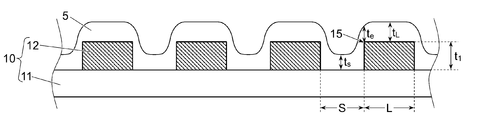
- FIG. 1 is a schematic cross-sectional view showing an embodiment of a printed wiring board, and an insulating resin layer 5 is provided on a wiring board 10 having a conductor pattern 12 on an insulating substrate 11.
- the printed wiring board may be a rigid wiring board using a rigid substrate or a flexible wiring board using a flexible substrate, and may have both a flexible portion and a rigid portion.
- a wiring pattern made of a conductor layer such as copper is provided on a flexible insulating resin substrate such as a polyimide film.
- the thickness of the conductor layer forming the wiring pattern is 10 to 35 ⁇ m, whereas in the thick conductor wiring board used in the present invention, the thickness of the conductor pattern 12 is 50 ⁇ m or more.
- the wiring board 10 including the conductor pattern 12 having a thickness of 50 ⁇ m or more is used.
- the upper limit of the thickness of the conductor pattern 12 is not particularly limited, but is preferably 150 ⁇ m or less, and more preferably 100 ⁇ m or less, from the viewpoint of improving the coverage with the insulating layer 5.
- flexibility can be maintained if the thickness of the conductor pattern is 100 ⁇ m or less.
- the thickness of the conductor pattern is 100 ⁇ m or less in order to maintain flexibility. It is preferable.
- the thickness of the conductor pattern 12 is particularly preferably in the range of about 60 to 80 ⁇ m.
- an insulating resin composition (solder resist ink) is applied by screen printing onto the thick conductor wiring 12 of the thick conductor wiring board 10 and the insulating substrate 11 between the thick conductor wirings, and then cured.
- a printed wiring board can be obtained in which the covering property of the conductor by the insulating layer and the embedding property of the insulating layer between the conductors are secured.
- the resin composition has predetermined solution characteristics (solid content concentration, viscosity and thixotropic index) described later, and the composition is not particularly limited as long as an insulating layer can be formed on the wiring board by screen printing.
- a composition having the same composition as that of a resist ink for general printed wiring boards can be used.
- a thermosetting or photocurable resin composition is preferable.
- the resin composition may be a light / thermosetting composition including both a thermosetting component and a photocurable component.
- the resin composition generally includes a binder polymer and a solvent.
- the binder polymer is not particularly limited as long as it is soluble in the solvent.
- the weight molecular weight of the binder polymer is preferably 1,000 to 1,000,000. When the molecular weight of the binder polymer is in the above range, the solubility in a solvent is excellent, and the viscosity of the resin composition can be adjusted appropriately.
- the weight average molecular weight is determined in terms of polyethylene glycol by gel permeation chromatography (GPC).
- Binder polymers include polyurethane resins, poly (meth) acrylic resins, polyvinyl resins, polystyrene resins, polyethylene resins, polypropylene resins, polyimide resins, polyamide resins, polyacetal resins, polycarbonate resins, polyesters. Resin, polyphenylene ether resin, polyphenylene sulfide resin, polyether sulfone resin, polyether ether ketone resin, and the like.
- the resin composition preferably contains a polyurethane resin as a binder polymer.
- the polyurethane resin is obtained by a reaction between a polyol compound and a polyisocyanate compound.
- long-chain diols such as polyalkylene glycol, polyoxyalkylene diol, polyester diol, polycarbonate diol, and polycaprolactone diol are used, the elastic modulus of the insulating layer obtained by curing of the resin composition decreases, so that the flexibility Tends to improve and warpage decreases.
- the polyisocyanate compound various aromatic polyisocyanate compounds and aliphatic polyisocyanate compounds are used.
- a polymer having a polymerizable group such as a (meth) acryloyl group and a soluble group such as a carboxyl group can be suitably used as the binder polymer.
- the solvent is not particularly limited as long as it can dissolve a resin component such as a binder polymer, and includes sulfoxides, formamides, acetamides, pyrrolidones, acetates, ethers, hexamethylphosphoramide, ⁇ -butyrolactone, and the like.
- a polar organic solvent is preferably used. These polar organic solvents can also be used in combination with aromatic hydrocarbons such as xylene and toluene.
- the amount of solvent in the resin composition may be adjusted so that desired solution characteristics can be obtained. In order to dissolve the resin component and obtain a solution suitable for screen printing, it is preferable to adjust the amount of the solvent so that the solid content concentration of the resin composition is 40 to 70 wt%.
- the thermosetting or photocurable resin composition includes a curable resin component.
- the thermosetting resin composition preferably contains a thermosetting resin component in addition to the binder polymer and the solvent.
- the thermosetting resin component is a compound that generates a crosslinked structure by heating and functions as a thermosetting agent. When the thermosetting resin component generates a crosslinked structure, the heat resistance, chemical resistance and electrical insulation reliability of the insulating layer can be improved.
- the photocurable resin composition contains a radical polymerizable compound and a photopolymerization initiator in addition to the binder polymer and the solvent.
- the photocurable resin composition may further contain a thermosetting resin component or a carboxyl group-containing resin as necessary.
- the photocurable resin composition containing a carboxyl group-containing resin can be used as an alkali development type resist suitable for processing a fine pattern.
- Thermosetting resin component include epoxy resins, bismaleimide resins, bisallyl nadiimide resins, acrylic resins, methacrylic resins, hydrosilyl cured resins, allyl cured resins, unsaturated polyester resins, and the like; Examples thereof include a side chain reactive group type thermosetting polymer having a reactive group such as an allyl group, vinyl group, alkoxysilyl group, hydrosilyl group at the side chain or at the terminal.
- the epoxy resin may be any of a monomer, an oligomer, and a polymer as long as it has at least one epoxy group in the molecule. Among these, a polyfunctional epoxy resin containing two epoxy groups in the molecule is preferable.
- Polyfunctional epoxy resins include bisphenol A type epoxy resin, bisphenol F type epoxy resin, bisphenol S type epoxy resin, hydrogenated bisphenol A type epoxy resin, biphenyl type epoxy resin, phenoxy type epoxy resin, naphthalene type epoxy resin, phenol novolac Type epoxy resin, cresol novolac type epoxy resin, trisphenolmethane type epoxy resin, dicyclopentadiene type epoxy resin, amine type epoxy resin, urethane modified epoxy resin, rubber modified epoxy resin, chelate modified epoxy resin and the like.
- epoxy resin curing agent examples include phenol resins such as phenol novolac resin, cresol novolac resin, naphthalene type phenol resin, amino resin, urea resin, melamine, and dicyandiamide.
- epoxy resin curing accelerators include phosphine compounds, amine compounds, and borate compounds, imidazoles, imidazolines, and azine imidazoles.
- the carboxyl group-containing resin is a compound having at least one carboxyl group in the molecule.
- the carboxyl group-containing resin preferably contains at least one photopolymerizable functional group in the molecule.
- the weight average molecular weight in terms of polyethylene glycol of the carboxyl group-containing compound is preferably 3,000 to 300,000. If the weight average molecular weight is within the above range, an excessive increase in the viscosity of the resin composition is suppressed, and further, the developability, flexibility, and chemical resistance of the photocurable resin composition tend to be improved.
- the acid value of the carboxyl group-containing resin measured by the method defined in JIS K5601-2-1 is preferably 50 to 200 mgKOH / g, more preferably 50 to 150 mgKOH / g.
- an insulating layer having low hygroscopicity, excellent electrical insulation reliability, and excellent developability can be obtained.
- carboxyl group-containing resin examples include a carboxyl group-containing (meth) acrylic copolymer, a carboxyl group-containing vinyl copolymer, acid-modified polyurethane, acid-modified polyester, acid-modified polycarbonate, acid-modified polyamide, and acid-modified polyimide. Is mentioned.
- an acrylic copolymer containing (meth) acrylic acid and (meth) acrylic acid alkyl ester as a copolymerization monomer component is preferable because of excellent photosensitivity, flexibility, and chemical resistance.
- the radical polymerizable compound is a compound that is polymerized by radicals generated by light or heat, and is preferably a compound having at least one unsaturated double bond in the molecule.
- the functional group having an unsaturated double bond is preferably an acrylic group, a methacryloyl group or a vinyl group.
- an EO-modified di (meth) acrylate or a polyfunctional (meth) acrylic compound having three or more (meth) acryloyl groups in one molecule is preferable.
- the number of repeating units of EO (ethylene oxide) contained in one molecule of di (meth) acrylate is preferably 2 to 50, and more preferably 2 to 40.
- an epoxy-modified (meth) acrylic resin in addition to the above, an epoxy-modified (meth) acrylic resin, a urethane-modified (meth) acrylic resin, a polyester-modified (meth) acrylic resin, or the like may be used.
- an epoxy-modified (meth) acrylic resin a urethane-modified (meth) acrylic resin, a polyester-modified (meth) acrylic resin, or the like may be used.
- the photopolymerizable resin composition preferably contains a photopolymerization initiator.
- the photopolymerization initiator is a compound that is activated by light energy such as UV, and initiates and accelerates the photopolymerization reaction such as the above-mentioned radical polymerizable compound, and various known photoradical generators can be appropriately selected and used. Good. It is desirable to use a mixture of two or more photopolymerization initiators.
- the resin composition preferably contains a filler.
- a filler an organic filler, an inorganic filler, an organic-inorganic composite filler, or the like may be appropriately selected and used.
- the organic filler material include poly (meth) acrylic acid alkyl ester, crosslinked poly (meth) acrylic acid alkyl ester, crosslinked styrene, nylon, silicone, crosslinked silicone, and crosslinked urethane.
- Examples of the inorganic filler material include metal oxides such as silica, titanium oxide, and alumina; metal nitrides such as silicon nitride and boron nitride; metal salts such as calcium carbonate, calcium hydrogen phosphate, calcium phosphate, and aluminum phosphate. It is done.
- Examples of the organic-inorganic composite filler include those in which an inorganic layer is formed on the surface of organic fine particles, and those in which an organic layer or organic fine particles are formed on the surface of inorganic fine particles.
- a filler whose surface is modified with a silane coupling agent or the like may be used. From the viewpoint of improving the insulation reliability between the wirings, an organic filler is preferable.
- the shape of the filler includes a spherical shape, a powder shape, a fiber shape, a needle shape, a scale shape, and the like.
- Spherical fillers are preferred because they have no anisotropy and stress is less likely to be unevenly distributed, so that the generation of distortion is suppressed and the warpage of the substrate due to curing shrinkage or the like tends to be reduced.
- spherical organic fillers are preferable from the viewpoint of improving the flexibility of the insulating layer after curing and suppressing warpage of the substrate, and crosslinked urethane beads containing urethane bonds in the molecule are particularly preferable.
- the filler content in the resin composition is 5 to 50 parts by weight with respect to 100 parts by weight of the total solid content.
- the amount is preferably 10 to 40 parts by weight.
- the average particle diameter of the filler is, for example, about 0.01 to 20 ⁇ m. Since a filler having a large particle diameter causes poor insulation, it is preferable to use classified spherical organic beads. Specifically, it is preferable to use a spherical filler having a number ratio of 99.99% or more with a particle diameter of 15 ⁇ m or less.
- the particle diameter can be measured by a laser diffraction / scattering particle diameter distribution measuring apparatus, and the volume-based median diameter is defined as the average particle diameter.
- Resin compositions include photochromic agents, thermochromic inhibitors, plasticizers, dyes, pigments, colorants, antifoaming agents, flame retardants, stabilizers, adhesion-imparting agents, leveling agents, and antioxidants as necessary.
- Various additives such as may be contained.
- Examples of the flame retardant include phosphoric ester compounds, halogen-containing compounds, metal hydroxides, organic phosphorus compounds, and silicones. Among these, phosphorus flame retardants are preferable.
- a resin composition is prepared by mixing the above components. You may grind
- the pulverization / dispersion may be performed using a general kneading apparatus such as a bead mill, a ball mill, or a three roll.
- a method for adding the filler to the resin composition (1) a method in which the resin composition is directly mixed using a stirrer or the like, and (2) addition to the polymerization reaction solution before or during the polymerization of the polymer in the resin composition. (3) A method of mixing with a polymer for a resin composition and other necessary components, and kneading or dispersing by a stress such as a shearing stress such as a three-roll roll or a bead mill. In order to disperse the filler satisfactorily and stabilize the dispersion state, a dispersant, a thickener and the like can also be used.
- the resin composition preferably has a viscosity at 25 ° C. of 50 to 300 poise and a thixotropic index of 1.1 to 3.5.
- the viscosity of the resin composition is a value measured at a rotation speed of 50 rpm using a B-type viscometer.
- the Chixolo topic index is the ratio of the measured viscosity value at 5 rpm and the measured viscosity value at 50 rpm.
- the solution viscosity of the resin composition is more preferably 100 to 300 poise, further preferably 130 to 270 poise, and particularly preferably 150 to 250 poise.
- the thixotropic index of the resin composition is more preferably 1.5 to 3.3, and further preferably 2.0 to 3.2.
- Viscosity and thixotropic properties of the resin composition by controlling the molecular weight of the binder polymer, introducing substituents into the binder polymer, controlling the amount of filler and the particle size of the filler, adding a resin component at room temperature such as a reactive monomer, etc.
- the index can be controlled within the above range.
- the solid content concentration of the resin composition is preferably 40 to 70 wt%, more preferably 45 to 69 wt%, and further preferably 50 to 68 wt%.
- the solid content concentration is a value measured under a drying condition of 170 ° C. ⁇ 1 hour in accordance with JIS K 5601-1-2.
- a resin composition is printed by screen printing on the wiring 12 forming region L of the thick conductor wiring board 10 and the insulating substrate 11 between the conductor patterns S, dried to remove the solvent, and the resin composition is cured as necessary. By doing so, an insulating layer is formed.
- the screen printing method is a method in which printing is performed by scanning a printing squeegee on a screen printing plate on which a resin composition is placed, and transferring the resin composition to a substrate to be printed.
- the resin composition can be applied only to the required area, so that the material use efficiency is high.
- the screen printing method has an advantage of excellent productivity because it is easy to form an insulating layer over a large area, and the throughput is high with a simple process.
- a screen printing plate having a thickness D of 2.2 times or more the yarn wire diameter d is used. Thickness is the thickness of the mesh woven with warp and weft constituting the screen printing plate, and the wire diameter is the diameter of the yarn constituting the mesh. If the mesh has the same woven structure, the thickness D depends on the wire diameter d. The larger the wire diameter, the thicker the thickness and the thicker the printed film thickness.
- the thickness D of the screen printing plate having a general woven structure is about twice the wire diameter d of the yarn.
- the thickness D is approximately twice the yarn diameter d
- the thickness D increases as the yarn diameter d increases.
- the opening becomes smaller, so when printing a resin composition with a large viscosity or thixotropy, the leveling property is insufficient, so the embedding property of the resin composition between the wirings decreases.
- the thickness D is 2.2 times or more the yarn wire diameter d
- the thickness can be increased without reducing the mesh opening, so the printing leveling property of the insulating layer is improved. Therefore, even when the viscosity or thixotropy of the resin composition is large, the wiring on the thick conductor wiring and between the wiring can be satisfactorily covered with the insulating layer.
- the thickness D of the screen printing plate is preferably 0.8 times or more, more preferably 1.0 times or more, and more preferably 1.5 times or more the thickness t 1 of the conductor wiring. preferable.
- the thickness D of the screen printing plate is preferably 3.5 times or less, more preferably 3 or less, and even more preferably 2.8 times or less of the thickness t 1 of the conductor wiring.
- the thickness D of the screen printing plate is preferably 40 to 200 ⁇ m, more preferably 70 to 190 ⁇ m, and further preferably 80 to 180 ⁇ m.
- the thickness D of the screen printing plate is preferably 2.3 to 4.4 times the wire diameter d, more preferably 2.5 to 3.5 times.
- the ShaAtsu of screen printing plate by adjusting the above range, the thickness of the insulating layer on the conductor pattern can be adjusted to 0.1 to 1 times the conductor thickness t 1.
- the thickness of the insulating layer on the conductor pattern is 0.3 to 0.7 times the conductor thickness t 1 is preferred.
- the screen printing plate is formed by knitting a minimum unit of a woven structure from at least one warp and at least one weft, and includes plain weave, twill, plain tatami and twill woven mesh fabrics, etc.
- the structure in which the warp yarn is woven in a substantially straight weft (hereinafter referred to as “thick weave structure”) has a thickness D of more than twice the wire diameter d of the yarn.
- weft yarns stretched with relatively high tension are arranged on the same plane in a straight state without substantially wavy, and warp yarns are greatly waved by stretching warp yarns with relatively low tension. It becomes a hit state and the thickness increases.
- a thick woven screen mesh a thick woven stainless steel mesh (3D-mesh, 3D-165-126) manufactured by Asada Mesh Co., Ltd. is preferably used.
- the weft yarns are alternately shifted in the vertical direction (normal direction of the printing surface). Both warp and weft contact.
- the weft yarn is positioned substantially on the same plane, the warp yarn has a high curvature and undulates up and down, and therefore the weft yarn does not contact the substrate.
- Thick weave printing plates have a small contact area with the substrate, and the resin composition is filled up to the bottom of the screen printing plate (the contact surface with the substrate), so the printed film thickness tends to increase further. It is suitable for printing a resin composition on a thick conductor wiring board.
- the material of the screen printing plate is not particularly limited, and various metal materials such as synthetic fibers such as polyester and nylon, stainless steel, nickel, nickel alloy, titanium, titanium alloy, and copper can be used.
- squeegee used for screen printing those having a squeegee hardness of 55 to 85 ° are particularly preferably used.
- the squeegee hardness is less than 55 °, the pressing force against the substrate to be printed is small, and the embedding property of the insulating layer between the wirings tends to be lowered. If the squeegee hardness is greater than 85 °, the coverage of the insulating layer on the wiring may be reduced.
- the attack angle when the squeegee contacts the screen printing plate is preferably 60 to 90 °.
- the thickness t L of the insulating layer on the thick conductor wiring and the thickness t s of the insulating layer between the wirings (between the conductor patterns) are respectively set to 10 to 100% of the conductor thickness t 1 and 50 It can be controlled to ⁇ 200%.
- the attack angle is smaller than 60 °, the pressing force against the substrate to be printed is small, and the embedding property of the insulating layer between the wirings tends to be lowered.
- the attack angle is larger than 90 °, the discharge amount of the resin composition is decreased, and the coverage of the insulating layer on the wiring may be decreased.
- the insulating film 5 is formed by drying the coating film.
- the drying temperature is preferably 120 ° C. or lower, more preferably 40 to 100 ° C.
- thermosetting is performed after drying.
- a heat-reactive functional group such as an epoxy group by heat treatment
- an insulating layer having excellent heat resistance can be obtained.
- the curing temperature is preferably 100 to 250 ° C, more preferably 120 to 200 ° C, and further preferably 130 to 180 ° C.
- An insulating layer 5 after heat curing is preferably the thickness t L on the wiring is not less than 0.1 times the conductor thickness t 1, the thickness t S between lines than 0.5 times the conductor thickness t 1 Preferably there is.
- Insulating layer 5 after heat curing is preferably the thickness t L on the wiring is less than 1 times the conductor thickness t 1, it is preferable that the thickness t S between the wires is less than 2 times the conductor thickness t 1 . If the thickness of the insulating layer is in the above range, warping of the wiring board due to curing shrinkage of the insulating layer can be suppressed.
- the thickness t S of the insulating layer between the conductor patterns of the wiring board is 0.5 to 2 times the thickness of the conductor thickness t 1 .
- the thickness t S of the insulating layer between the preferred circuit board of the conductor pattern is 0.7 to 1.7 times the conductor thickness t 1, more preferably 0.9 to 1.5 times the conductor thickness t 1 .
- a layer (solder resist) can be formed.
- the thickness t L of the insulating layer on the conductor pattern is preferably 0.3 to 0.7 times the conductor thickness t 1 .
- a thickness t e of the insulating layer 5 on the edge 15 of the conductor pattern is 0.1 to 1 times the conductor thickness t 1 is preferably from 0.3 to 0 0.7 times is more preferable.
- the thickness t e of the insulating layer 5 on the edge 15, or 0.3 times the thickness t L of the center of the insulating layer of the conductor pattern is preferred.
- an insulating layer having a predetermined thickness and excellent coverage can be formed on a thick conductor wiring board by using a resin composition having a predetermined thixotropy and a screen printing plate having a predetermined thickness. .
- ⁇ Formulation Examples 1 to 12 Preparation of resin composition> Binder polymer, epoxy resin, curing accelerator, radical polymerizable polyfunctional acrylate, filler, solvent and other components (photopolymerization initiator, flame retardant, colorant, and antifoaming agent) are shown in Table 1 as formulation example 1. After blending with a composition of ⁇ 12 and mixing with a stirrer equipped with a general stirring blade, the mixture was passed twice with a three-roll mill to obtain a uniform solution.
- a binder polymer (total 82 parts by weight), a curing agent (1 part by weight), a polyfunctional acrylate (total 15 parts by weight), a photopolymerization initiator (total 3.3 parts by weight), a colorant ( The composition of 1.2 parts by weight in total) and the antifoaming agent (2.5 parts by weight) are common, and by changing the type and content of epoxy resin, flame retardant, filler and solvent, the characteristics of the solution ( Solid content concentration and viscosity) were adjusted. In Formulation Example 11, since the solid content concentration was large, it was difficult to prepare the resin composition.
- the particle diameters of the resin compositions of Formulation Examples 1 to 10 were measured with a grindometer, and all were 10 ⁇ m or less. After defoaming the solution with a defoamer, the following evaluation was performed.
- Viscosity and thixotropic index In an environment of 25 ° C., the viscosity of the resin compositions of alignment examples 1 to 10 was measured at a rotation speed of 5 rpm and 50 rpm with a B-type viscometer (Brookfield, rotor No. 4), and the viscosity measured at 5 rpm. The thixotropic index was calculated from the ratio of the viscosity measured at 50 rpm.
- Table 1 shows the composition and solution characteristics (solid content concentration, viscosity (measured value at 50 rpm) and thixotropic index) of Formulation Examples 1-12.
- methyltriglyme is the total amount including the solvent contained in the polymer solution of Synthesis Example 1.
- ⁇ Formation of insulating layer on thick conductor wiring board> Using the above resin composition, a thick conductor with an attack angle of 75 ° using a rubber squeegee with a squeegee hardness of 75 ° (manufactured by Mino Group) using a screen printer (product name “Minomat 5575” manufactured by Mino Group) Screen printing was performed on the wiring board, dried at 80 ° C. for 20 minutes, and then gradually cooled to room temperature. Then, it heat-hardened at 150 degreeC for 30 minutes, and formed the insulating layer in the thick conductor wiring board.
- a flexible wiring board manufactured by Taiyo Kogyo Co., Ltd.
- a rolled copper wiring thickness 70 ⁇ m
- a polyimide film with a thickness of 25 ⁇ m
- Production Examples 1 to 5 the following stainless mesh screen printing plates were used.
- the insulating layer was formed using all the resin compositions of Formulation Examples 1 to 10.
- insulating layers were formed using the resin compositions of Formulation Examples 1 to 5 and Formulation Examples 8 to 10.
- the thickness of the insulating layer on the polyimide substrate on the thick conductor wiring and between the wirings (between the conductor patterns) was measured by cross-sectional microscope observation of the test piece obtained above, and evaluated according to the following criteria.
- the insulating layer thickness is 7 ⁇ m or more and less than 21 ⁇ m (10% or more and less than 30% of the conductor thickness)
- C Insulating layer thickness less than 7 ⁇ m (less than 10% of conductor thickness) (Coverage between wiring)
- C Insulating layer thickness of less than 35 ⁇ m (less than 50% of conductor thickness)
- test piece was cut into an area of 75 mm ⁇ 55 mm around the wiring and placed on a smooth table so that the insulating layer was on the upper surface, and the distance between the table and the end of the test piece was measured.
- Table 2 shows the evaluation results of the coverage and warpage of the insulating layers of the printed wiring boards obtained in Production Examples 1 to 5.
- the resin composition of Formulation Example 8 having a high viscosity, the resin composition of Formulation Example 9 having a low viscosity, and the resin composition of Formulation Example 10 having a high thixotropic index have printability by screen printing. It can be seen that, even when any screen printing plate is used, the insulating layer cannot sufficiently cover the wiring and between the wirings. In the resin compositions of Formulation Examples 1 to 5, in Preparation Example 1 using the screen printing plate having a thickness of 2.1 times the wire diameter, the coverage on the wiring and / or between the wirings was not sufficient. In Production Examples 2 to 5 using the screen printing plate having a thickness of 2.2 times or more of the wire diameter, the coverage with the insulating layer on the wiring and between the wirings was improved.
Landscapes
- Engineering & Computer Science (AREA)
- Microelectronics & Electronic Packaging (AREA)
- Chemical & Material Sciences (AREA)
- Health & Medical Sciences (AREA)
- Chemical Kinetics & Catalysis (AREA)
- Medicinal Chemistry (AREA)
- Polymers & Plastics (AREA)
- Organic Chemistry (AREA)
- Manufacturing & Machinery (AREA)
- Mechanical Engineering (AREA)
- Non-Metallic Protective Coatings For Printed Circuits (AREA)
- Compositions Of Macromolecular Compounds (AREA)
Abstract
This printed wiring board has conductor patterns (12) for which the thickness t1 is at least 50 µm provided on an insulated substrate (11), an insulating layer (5) being provided on a conductor pattern (L) and on an insulated substrate between conductor patterns (S). The thickness tL of the insulating layer on the conductor patterns is preferably 0.1-1 times the conductor thickness t1. The insulating layer is formed by printing a resin composition on the conductor patterns and on the insulated substrate between conductor patterns using screen printing, and subsequently curing. The resin composition has a viscosity of 50-300 P at 25°C, and a thixotropic index of 1.1-3.5. The screen printing plate used for screen printing has a thickness of at least 2.2 times the thread diameter.
Description
本発明は、導体パターン上に絶縁層を備えるプリント配線板、およびその製造方法に関する。
The present invention relates to a printed wiring board having an insulating layer on a conductor pattern, and a method for manufacturing the same.
プリント配線板の表面には、配線板を被覆し保護するとともに、配線間の絶縁を維持するための絶縁層としてソルダーレジストが設けられている。ソルダーレジストとしては、カバーレイフィルムおよびカバーコートインク等が用いられている。
The surface of the printed wiring board is provided with a solder resist as an insulating layer for covering and protecting the wiring board and maintaining insulation between the wirings. As the solder resist, a cover lay film, a cover coat ink, or the like is used.
近年、電磁誘導を利用したワイヤレス給電システムが実用化に至っている。ワイヤレス給電システムでは、送受電の効率を高めるために、例えば50μm以上の厚みを有する導体パターンを備えるプリント配線板が用いられる(例えば、特許文献1参照)。このような厚い導体パターン(以下「厚導体配線」と称する)を備える配線板(以下「厚導体配線板」と称する)においても、配線板の表面を絶縁性の保護層で被覆する必要がある。
In recent years, wireless power feeding systems using electromagnetic induction have come into practical use. In the wireless power feeding system, a printed wiring board including a conductor pattern having a thickness of, for example, 50 μm or more is used in order to increase power transmission / reception efficiency (for example, see Patent Document 1). Even in a wiring board (hereinafter referred to as “thick conductor wiring board”) having such a thick conductor pattern (hereinafter referred to as “thick conductor wiring”), it is necessary to cover the surface of the wiring board with an insulating protective layer. .
一般的なフレキシブルプリント配線板(導体厚み:10~40μm程度)に用いられているカバーコートインクを厚導体配線板上に印刷すると、絶縁層の膜厚が極端に薄い部分や絶縁層により被覆されずに導体が露出する部分が生じることがあり、特に、配線のエッジ部分で導体が露出しやすい。そのため、厚導体配線板の絶縁保護層としてはカバーレイフィルムが用いられることが多い。一方、厚導体配線板の絶縁保護層としてカバーレイフィルムを用いると、配線の側面近傍の段差部分において、配線とカバーレイフィルムとの間への空隙の残存が問題となる場合がある(例えば、特許文献2参照)。
When the cover coat ink used for general flexible printed wiring boards (conductor thickness: about 10-40μm) is printed on the thick conductor wiring board, the insulating layer is covered with an extremely thin part or insulating layer. In some cases, a portion where the conductor is exposed is generated. In particular, the conductor is easily exposed at an edge portion of the wiring. Therefore, a coverlay film is often used as the insulating protective layer of the thick conductor wiring board. On the other hand, when a coverlay film is used as an insulating protective layer of a thick conductor wiring board, in the step portion near the side surface of the wiring, there may be a problem of remaining voids between the wiring and the coverlay film (for example, Patent Document 2).
導体の露出や、導体と絶縁層との間の空隙は、プリント配線板の品質を低下させるだけでなく、配線板の発熱や電気ショートの原因ともなる。特許文献2は、厚導体配線板上に絶縁樹脂層をスクリーン印刷した後、その上に同様の絶縁樹脂材料からなる接着シートを積層することにより、導体の露出および導体と絶縁層との間の空隙の問題を解決できることを開示している。
The exposure of the conductor and the gap between the conductor and the insulating layer not only deteriorate the quality of the printed wiring board but also cause the wiring board to generate heat and cause an electrical short circuit. In Patent Document 2, after an insulating resin layer is screen-printed on a thick conductor wiring board, an adhesive sheet made of the same insulating resin material is laminated thereon, thereby exposing the conductor and between the conductor and the insulating layer. It discloses that the problem of voids can be solved.
特許文献2の方法では、配線板上に塗布した絶縁樹脂層を半硬化の状態で保持し、その上に接着シートを積層加熱して一体化する必要があるため、工程が煩雑であり、材料コストも高い。
In the method of Patent Document 2, it is necessary to hold the insulating resin layer applied on the wiring board in a semi-cured state, and stack and heat the adhesive sheet on the insulating sheet. Cost is high.
このような背景に基づき、本発明は、厚導体配線を有するプリント配線板上への樹脂組成物の塗布により、厚導体配線上に絶縁層が良好に被覆され、かつ厚導体配線の間隙に絶縁層が良好に埋設された厚導体配線板を提供することを目的とする。
Based on such a background, the present invention provides a coating of a resin composition on a printed wiring board having a thick conductor wiring so that an insulating layer is satisfactorily coated on the thick conductor wiring and insulated in the gaps of the thick conductor wiring. An object of the present invention is to provide a thick conductor wiring board in which layers are well embedded.
本発明者らは上記課題を解決すべく鋭意研究した結果、所定の溶液特性を有する樹脂組成物を、所定のスクリーン印刷版を用いてスクリーン印刷することにより、厚導体配線板上を絶縁層により良好に被覆し、かつ導体パターンの間隙に絶縁層を良好に埋設できることを見出した。
As a result of intensive studies to solve the above-mentioned problems, the present inventors screen-printed a resin composition having a predetermined solution characteristic using a predetermined screen printing plate, thereby forming an insulating layer on the thick conductor wiring board. It has been found that the insulating layer can be satisfactorily embedded in the gap between the conductor patterns with good coating.
本発明は、絶縁基板上に厚み50μm以上の導体パターンを備え、導体パターン上および導体パターン間の絶縁基板上に絶縁層が設けられているプリント配線板およびその製造方法に関する。一実施形態のプリント配線板は、絶縁基板として可撓性の樹脂基板を用いたフレキシブルプリント配線板である。絶縁基板は可撓性部分と剛性部分とを有していてもよい。配線板の可撓性を維持するためには、可撓性の基板上に設けられた導体の厚みは100μm以下が好ましい。
The present invention relates to a printed wiring board provided with a conductor pattern having a thickness of 50 μm or more on an insulating substrate, and an insulating layer provided on the conductor pattern and between the conductor patterns, and a manufacturing method thereof. The printed wiring board of one embodiment is a flexible printed wiring board using a flexible resin substrate as an insulating substrate. The insulating substrate may have a flexible part and a rigid part. In order to maintain the flexibility of the wiring board, the thickness of the conductor provided on the flexible substrate is preferably 100 μm or less.
良好な絶縁性を確保するために、導体パターン間の絶縁層の厚みは、導体厚みの0.5~2倍が好ましい。導体パターン上の絶縁層の厚みは、導体パターンの中央およびエッジにおいて、いずれも導体厚みの0.1~1倍が好ましく、0.3~0.7倍が好ましい。導体パターンのエッジ上の絶縁層の厚みは、導体パターンの中央上の絶縁層の厚みの0.3倍以上が好ましい。
In order to ensure good insulation, the thickness of the insulating layer between the conductor patterns is preferably 0.5 to 2 times the conductor thickness. The thickness of the insulating layer on the conductor pattern is preferably 0.1 to 1 times, more preferably 0.3 to 0.7 times the conductor thickness at the center and edge of the conductor pattern. The thickness of the insulating layer on the edge of the conductor pattern is preferably 0.3 times or more the thickness of the insulating layer on the center of the conductor pattern.
導体パターン上および導体パターン間の絶縁基板上に、樹脂組成物をスクリーン印刷により印刷した後、硬化させることにより、絶縁層が形成される。絶縁層を形成するための樹脂組成物は、25℃における粘度が50~300P、チクソトロピックスインデックスが1.1~3.5であるものが好ましい。
An insulating layer is formed by printing a resin composition on a conductive pattern and an insulating substrate between conductive patterns by screen printing and then curing the resin composition. The resin composition for forming the insulating layer preferably has a viscosity at 25 ° C. of 50 to 300 P and a thixotropic index of 1.1 to 3.5.
スクリーン印刷に用いられるスクリーン印刷版は、紗厚が糸の線径の2.2倍以上であるものが好ましい。紗厚が糸の線径の2.2倍以上のスクリーン印刷版の具体例としては、実質的に直線状の横糸に縦糸が織り込まれた構造のメッシュ織物等が挙げられる。スクリーン印刷版の紗厚は、40~200μmが好ましく、糸の線径の4.4倍以下が好ましい。スクリーン印刷に用いるスキージの硬度は55~85°が好ましく、アタック角度は60~90°が好ましい。
The screen printing plate used for screen printing preferably has a thickness of 2.2 or more times the wire diameter of the yarn. Specific examples of the screen printing plate having a cocoon thickness of 2.2 times or more the yarn diameter include a mesh fabric having a structure in which warp yarns are woven into substantially straight weft yarns. The thickness of the screen printing plate is preferably 40 to 200 μm, and is preferably 4.4 times or less of the wire diameter of the yarn. The hardness of the squeegee used for screen printing is preferably 55 to 85 °, and the attack angle is preferably 60 to 90 °.
樹脂組成物は、例えば、バインダーポリマー、溶媒、およびフィラーを含む。フィラーとしては球状の有機フィラーが好ましい。バインダーポリマーとしては例えばウレタン系ポリマーが用いられる。樹脂組成物は、エポキシ樹脂を含んでいてもよい。樹脂組成物は、分子内にカルボキシ基および重合性基を有する化合物を含んでいてもよい。樹脂組成物は、光重合開始剤を含んでいてもよい。樹脂組成物の固形分濃度は40~70wt%程度が好ましい。
The resin composition includes, for example, a binder polymer, a solvent, and a filler. As the filler, a spherical organic filler is preferable. For example, a urethane polymer is used as the binder polymer. The resin composition may contain an epoxy resin. The resin composition may contain a compound having a carboxy group and a polymerizable group in the molecule. The resin composition may contain a photopolymerization initiator. The solid content concentration of the resin composition is preferably about 40 to 70 wt%.
本発明の方法では、樹脂組成物の塗布のみにより、厚導体配線上を絶縁層により良好に被覆し、かつ厚導体配線の間隙に絶縁層を良好に埋設できるため、電気ショート等の不具合が抑制された厚導体配線板の生産性を向上できる。本発明のプリント配線板は、ワイヤレス給電用の配線板等の種々の用途に使用できる。
In the method of the present invention, the thick conductor wiring can be satisfactorily covered with the insulating layer and the insulating layer can be satisfactorily embedded in the gap of the thick conductor wiring only by applying the resin composition, thereby suppressing problems such as electrical shorts. It is possible to improve the productivity of the thick conductor wiring board. The printed wiring board of the present invention can be used for various applications such as a wiring board for wireless power feeding.
図1は、プリント配線板の一形態を示す模式的断面図であり、絶縁基板11上に導体パターン12を備える配線板10上に、絶縁性の樹脂層5が設けられている。隣接する配線パターン間を埋めるように絶縁層が設けられることにより配線間の絶縁を確保できる。プリント配線板は剛性基板を用いたリジッド配線板でも可撓性基板を用いたフレキシブル配線板でもよく、可撓性部分と剛性部分の両方を有するものでもよい。フレキシブルプリント配線板や、可撓性部分と剛性部分を有するプリント配線板の可撓性部分では、ポリイミドフィルム等の可撓性絶縁樹脂基板上に銅等の導体層からなる配線パターンが設けられている。一般的なプリント配線板では配線パターンを形成する導体層の厚みは10~35μmであるのに対して、本発明に用いられる厚導体配線板では、導体パターン12の厚みが50μm以上である。
FIG. 1 is a schematic cross-sectional view showing an embodiment of a printed wiring board, and an insulating resin layer 5 is provided on a wiring board 10 having a conductor pattern 12 on an insulating substrate 11. By providing an insulating layer so as to fill in between adjacent wiring patterns, insulation between wirings can be ensured. The printed wiring board may be a rigid wiring board using a rigid substrate or a flexible wiring board using a flexible substrate, and may have both a flexible portion and a rigid portion. In a flexible printed wiring board or a flexible part of a printed wiring board having a flexible part and a rigid part, a wiring pattern made of a conductor layer such as copper is provided on a flexible insulating resin substrate such as a polyimide film. Yes. In a general printed wiring board, the thickness of the conductor layer forming the wiring pattern is 10 to 35 μm, whereas in the thick conductor wiring board used in the present invention, the thickness of the conductor pattern 12 is 50 μm or more.
例えば、ワイヤレス給電に利用される配線板では、送受電効率を高めるために配線の電気的抵抗を下げる必要があり、厚みが50μm以上の導体パターン12を備える配線板10が用いられる。導体パターン12の厚みの上限は特に限定されないが、絶縁層5による被覆性を高める観点から、150μm以下が好ましく、100μm以下がより好ましい。絶縁基板11としてポリイミドフィルム等の可撓性フィルムを用いたフレキシブル配線板では、導体パターンの厚みが100μm以下であれば、フレキシブル性を維持できる。可撓性部分と剛性部分とを有する絶縁基板の可撓性部分(可撓性フィルム上)に導体パターンを形成する場合も、可撓性を維持するために導体パターンの厚みが100μm以下であることが好ましい。導体パターン12の厚みは、60~80μm程度の範囲が特に好ましい。
For example, in a wiring board used for wireless power feeding, it is necessary to lower the electrical resistance of the wiring in order to increase power transmission / reception efficiency, and the wiring board 10 including the conductor pattern 12 having a thickness of 50 μm or more is used. The upper limit of the thickness of the conductor pattern 12 is not particularly limited, but is preferably 150 μm or less, and more preferably 100 μm or less, from the viewpoint of improving the coverage with the insulating layer 5. In a flexible wiring board using a flexible film such as a polyimide film as the insulating substrate 11, flexibility can be maintained if the thickness of the conductor pattern is 100 μm or less. Even when the conductor pattern is formed on the flexible portion (on the flexible film) of the insulating substrate having the flexible portion and the rigid portion, the thickness of the conductor pattern is 100 μm or less in order to maintain flexibility. It is preferable. The thickness of the conductor pattern 12 is particularly preferably in the range of about 60 to 80 μm.
本発明においては、厚導体配線板10の厚導体配線12上および厚導体配線間の絶縁性基板11上に、スクリーン印刷により絶縁性樹脂組成物(ソルダーレジストインク)を塗布し、次いで硬化することにより、絶縁層による導体の被覆性および導体間への絶縁層の埋め込み性を確保したプリント配線板が得られる。
In the present invention, an insulating resin composition (solder resist ink) is applied by screen printing onto the thick conductor wiring 12 of the thick conductor wiring board 10 and the insulating substrate 11 between the thick conductor wirings, and then cured. Thus, a printed wiring board can be obtained in which the covering property of the conductor by the insulating layer and the embedding property of the insulating layer between the conductors are secured.
[樹脂組成物]
樹脂組成物は、後述する所定の溶液特性(固形分濃度、粘度およびチクソトロピックインデックス)を有し、スクリーン印刷により配線板上に絶縁層を形成可能なものであれば組成は特に限定されず、一般のプリント配線板用のレジストインクと同様の組成のものを使用できる。配線板10上での絶縁層5の強度や耐溶剤性を高める観点から、熱硬化性又は光硬化性の樹脂組成物が好ましい。樹脂組成物は、熱硬化性成分と光硬化性成分の両方を備える光・熱硬化性組成物でもよい。樹脂組成物は、一般に、バインダーポリマーおよび溶媒を含む。 [Resin composition]
The resin composition has predetermined solution characteristics (solid content concentration, viscosity and thixotropic index) described later, and the composition is not particularly limited as long as an insulating layer can be formed on the wiring board by screen printing. A composition having the same composition as that of a resist ink for general printed wiring boards can be used. From the viewpoint of increasing the strength and solvent resistance of theinsulating layer 5 on the wiring board 10, a thermosetting or photocurable resin composition is preferable. The resin composition may be a light / thermosetting composition including both a thermosetting component and a photocurable component. The resin composition generally includes a binder polymer and a solvent.
樹脂組成物は、後述する所定の溶液特性(固形分濃度、粘度およびチクソトロピックインデックス)を有し、スクリーン印刷により配線板上に絶縁層を形成可能なものであれば組成は特に限定されず、一般のプリント配線板用のレジストインクと同様の組成のものを使用できる。配線板10上での絶縁層5の強度や耐溶剤性を高める観点から、熱硬化性又は光硬化性の樹脂組成物が好ましい。樹脂組成物は、熱硬化性成分と光硬化性成分の両方を備える光・熱硬化性組成物でもよい。樹脂組成物は、一般に、バインダーポリマーおよび溶媒を含む。 [Resin composition]
The resin composition has predetermined solution characteristics (solid content concentration, viscosity and thixotropic index) described later, and the composition is not particularly limited as long as an insulating layer can be formed on the wiring board by screen printing. A composition having the same composition as that of a resist ink for general printed wiring boards can be used. From the viewpoint of increasing the strength and solvent resistance of the
<バインダーポリマー>
バインダーポリマーは、溶媒に対して可溶性であれば特に限定されない。バインダーポリマーの重量分子量は1,000~1,000,000が好ましい。バインダーポリマーの分子量が上記範囲であれば、溶媒に対する溶解性に優れると共に、樹脂組成物の粘度を適切に調整できる。重量平均分子量は、ゲル・パーミエーション・クロマトグラフィー(GPC)により、ポリエチレングリコール換算で求められる。 <Binder polymer>
The binder polymer is not particularly limited as long as it is soluble in the solvent. The weight molecular weight of the binder polymer is preferably 1,000 to 1,000,000. When the molecular weight of the binder polymer is in the above range, the solubility in a solvent is excellent, and the viscosity of the resin composition can be adjusted appropriately. The weight average molecular weight is determined in terms of polyethylene glycol by gel permeation chromatography (GPC).
バインダーポリマーとしては、ポリウレタン系樹脂、ポリ(メタ)アクリル系樹脂、ポリビニル系樹脂、ポリスチレン系樹脂、ポリエチレン系樹脂、ポリプロピレン系樹脂、ポリイミド系樹脂、ポリアミド系樹脂、ポリアセタール系樹脂、ポリカーボネート系樹脂、ポリエステル系樹脂、ポリフェニレンエーテル系樹脂、ポリフェニレンスルフィド系樹脂、ポリエーテルスルホン系樹脂、ポリエーテルエーテルケトン系樹脂等が挙げられる。
Binder polymers include polyurethane resins, poly (meth) acrylic resins, polyvinyl resins, polystyrene resins, polyethylene resins, polypropylene resins, polyimide resins, polyamide resins, polyacetal resins, polycarbonate resins, polyesters. Resin, polyphenylene ether resin, polyphenylene sulfide resin, polyether sulfone resin, polyether ether ketone resin, and the like.
樹脂組成物は、バインダーポリマーとしてポリウレタン系樹脂を含むことが好ましい。ポリウレタン系樹脂は、ポリオール化合物とポリイソシアネート化合物との反応により得られる。
The resin composition preferably contains a polyurethane resin as a binder polymer. The polyurethane resin is obtained by a reaction between a polyol compound and a polyisocyanate compound.
ポリオール化合物としては、ポリオキシアルキレングリコール、ポリエステルジオール、ポリカーボネートジオール、ラクトン類の開環付加反応により得られるポリカプロラクトンジオール、ビスフェノール類、ビスフェノール類のアルキレンオキサイド付加物、水添ビスフェノール類、水添ビスフェノール類のアルキレンオキサイド付加物等が挙げられる。特に、ポリアルキレングリコール、ポリオキシアルキレンジオール、ポリエステルジオール、ポリカーボネートジオール、ポリカプロラクトンジオール等の長鎖ジオールを用いた場合、樹脂組成物の硬化により得られる絶縁層の弾性率が低下するため、屈曲性が向上し、反りが低減する傾向がある。ポリイソシアネート化合物としては、各種の芳香族ポリイソシアネート化合物および脂肪族ポリイソシアネート化合物が用いられる。
Polyol alkylene glycol, polyester diol, polycarbonate diol, polycaprolactone diol obtained by ring-opening addition reaction of lactones, bisphenols, alkylene oxide adducts of bisphenols, hydrogenated bisphenols, hydrogenated bisphenols And alkylene oxide adducts. In particular, when long-chain diols such as polyalkylene glycol, polyoxyalkylene diol, polyester diol, polycarbonate diol, and polycaprolactone diol are used, the elastic modulus of the insulating layer obtained by curing of the resin composition decreases, so that the flexibility Tends to improve and warpage decreases. As the polyisocyanate compound, various aromatic polyisocyanate compounds and aliphatic polyisocyanate compounds are used.
樹脂組成物が光硬化性の場合には、(メタ)アクリロイル基等の重合性基とカルボキシル基等の可溶性基とを有するポリマーを、バインダーポリマーとして好適に用いることができる。
When the resin composition is photocurable, a polymer having a polymerizable group such as a (meth) acryloyl group and a soluble group such as a carboxyl group can be suitably used as the binder polymer.
<溶媒>
溶媒は、バインダーポリマー等の樹脂成分を溶解できるものであれば特に限定されず、スルホキシド類、ホルムアミド類、アセトアミド類、ピロリドン類、アセテート類、エーテル類、ヘキサメチルホスホルアミド、γ-ブチロラクトン等の極性有機溶媒が好適に用いられる。これらの極性有機溶媒と、キシレン、トルエン等の芳香族炭化水素とを組み合わせて用いることもできる。樹脂組成物中の溶媒量は、所望の溶液特性が得られるように調整すればよい。樹脂成分を溶解させ、かつスクリーン印刷に適した溶液を得るために、樹脂組成物の固形分濃度が40~70wt%となるように溶媒量を調整することが好ましい。 <Solvent>
The solvent is not particularly limited as long as it can dissolve a resin component such as a binder polymer, and includes sulfoxides, formamides, acetamides, pyrrolidones, acetates, ethers, hexamethylphosphoramide, γ-butyrolactone, and the like. A polar organic solvent is preferably used. These polar organic solvents can also be used in combination with aromatic hydrocarbons such as xylene and toluene. The amount of solvent in the resin composition may be adjusted so that desired solution characteristics can be obtained. In order to dissolve the resin component and obtain a solution suitable for screen printing, it is preferable to adjust the amount of the solvent so that the solid content concentration of the resin composition is 40 to 70 wt%.
<硬化性樹脂成分>
熱硬化性又は光硬化性の樹脂組成物は、硬化性樹脂成分を含む。熱硬化性樹脂組成物は、バインダーポリマーおよび溶媒に加えて、熱硬化性樹脂成分を含有することが好ましい。熱硬化性樹脂成分は、加熱により架橋構造を生成し、熱硬化剤として機能する化合物である。熱硬化性樹脂成分が架橋構造を生成することにより、絶縁層の耐熱性、耐薬品性および電気絶縁信頼性を向上できる。光硬化性樹脂組成物は、バインダーポリマーおよび溶媒に加えて、ラジカル重合性化合物や光重合開始剤を含む。光硬化性樹脂組成物は、さらに必要に応じて、熱硬化性樹脂成分やカルボキシル基含有樹脂を含有していてもよい。カルボキシル基含有樹脂を含む光硬化性樹脂組成物は、微細パターンの加工に適したアルカリ現像型のレジストとして使用できる。 <Curable resin component>
The thermosetting or photocurable resin composition includes a curable resin component. The thermosetting resin composition preferably contains a thermosetting resin component in addition to the binder polymer and the solvent. The thermosetting resin component is a compound that generates a crosslinked structure by heating and functions as a thermosetting agent. When the thermosetting resin component generates a crosslinked structure, the heat resistance, chemical resistance and electrical insulation reliability of the insulating layer can be improved. The photocurable resin composition contains a radical polymerizable compound and a photopolymerization initiator in addition to the binder polymer and the solvent. The photocurable resin composition may further contain a thermosetting resin component or a carboxyl group-containing resin as necessary. The photocurable resin composition containing a carboxyl group-containing resin can be used as an alkali development type resist suitable for processing a fine pattern.
(熱硬化性樹脂成分)
熱硬化性樹脂成分としては、エポキシ樹脂、ビスマレイミド樹脂、ビスアリルナジイミド樹脂、アクリル樹脂、メタクリル樹脂、ヒドロシリル硬化樹脂、アリル硬化樹脂、不飽和ポリエステル樹脂等の熱硬化性樹脂;高分子鎖の側鎖又は末端にアリル基、ビニル基、アルコキシシリル基、ヒドロシリル基等の反応性基を有する側鎖反応性基型熱硬化性高分子等が挙げられる。 (Thermosetting resin component)
Thermosetting resin components include epoxy resins, bismaleimide resins, bisallyl nadiimide resins, acrylic resins, methacrylic resins, hydrosilyl cured resins, allyl cured resins, unsaturated polyester resins, and the like; Examples thereof include a side chain reactive group type thermosetting polymer having a reactive group such as an allyl group, vinyl group, alkoxysilyl group, hydrosilyl group at the side chain or at the terminal.
熱硬化性樹脂成分としてエポキシ樹脂を用いることにより、硬化により得られる絶縁層の耐熱性、および導体や絶縁性基板に対する接着性を向上できる。エポキシ樹脂は、分子中に少なくとも1つ以上のエポキシ基を有していれば、モノマー、オリゴマー、およびポリマーのいずれでもよい。中でも、分子内に2個のエポキシ基を含む多官能エポキシ樹脂が好ましい。多官能エポキシ樹脂としては、ビスフェノールA型エポキシ樹脂、ビスフェノールF型エポキシ樹脂、ビスフェノールS型エポキシ樹脂、水添ビスフェノールA型エポキシ樹脂、ビフェニル型エポキシ樹脂、フェノキシ型エポキシ樹脂、ナフタレン型エポキシ樹脂、フェノールノボラック型エポキシ樹脂、クレゾールノボラック型エポキシ樹脂、トリスフェノールメタン型エポキシ樹脂、ジシクロペンタジエン型エポキシ樹脂、アミン型エポキシ樹脂、ウレタン変性エポキシ樹脂、ゴム変性エポキシ樹脂、キレート変性エポキシ樹脂等が挙げられる。
By using an epoxy resin as the thermosetting resin component, it is possible to improve the heat resistance of the insulating layer obtained by curing and the adhesion to the conductor and the insulating substrate. The epoxy resin may be any of a monomer, an oligomer, and a polymer as long as it has at least one epoxy group in the molecule. Among these, a polyfunctional epoxy resin containing two epoxy groups in the molecule is preferable. Polyfunctional epoxy resins include bisphenol A type epoxy resin, bisphenol F type epoxy resin, bisphenol S type epoxy resin, hydrogenated bisphenol A type epoxy resin, biphenyl type epoxy resin, phenoxy type epoxy resin, naphthalene type epoxy resin, phenol novolac Type epoxy resin, cresol novolac type epoxy resin, trisphenolmethane type epoxy resin, dicyclopentadiene type epoxy resin, amine type epoxy resin, urethane modified epoxy resin, rubber modified epoxy resin, chelate modified epoxy resin and the like.
エポキシ樹脂の硬化剤としては、フェノールノボラック樹脂、クレゾールノボラック樹脂、ナフタレン型フェノール樹脂等のフェノール樹脂、アミノ樹脂、ユリア樹脂、メラミン、ジシアンジアミド等が挙げられる。エポキシ樹脂の硬化促進剤としては、ホスフィン系化合物、アミン系化合物、ボレート系化合物等、イミダゾール類、イミダゾリン類、アジン系イミダゾール類等が挙げられる。
Examples of the epoxy resin curing agent include phenol resins such as phenol novolac resin, cresol novolac resin, naphthalene type phenol resin, amino resin, urea resin, melamine, and dicyandiamide. Examples of epoxy resin curing accelerators include phosphine compounds, amine compounds, and borate compounds, imidazoles, imidazolines, and azine imidazoles.
(カルボキシル基含有樹脂)
カルボキシル基含有樹脂は、分子内に少なくとも1つのカルボキシル基を有する化合物である。アルカリ現像型のレジストとして用いられる光硬化性樹脂組成物では、カルボキシル基含有樹脂は、分子内に少なくとも1つの光重合性官能基を含んでいることが好ましい。カルボキシル基含有化合物のポリエチレングリコール換算の重量平均分子量は、3,000~300,000が好ましい。重量平均分子量が上記範囲内であれば、樹脂組成物の粘度の過度の上昇が抑制され、さらに、光硬化性樹脂組成物の現像性、柔軟性、および耐薬品性が向上する傾向がある。 (Carboxyl group-containing resin)
The carboxyl group-containing resin is a compound having at least one carboxyl group in the molecule. In the photocurable resin composition used as an alkali developing resist, the carboxyl group-containing resin preferably contains at least one photopolymerizable functional group in the molecule. The weight average molecular weight in terms of polyethylene glycol of the carboxyl group-containing compound is preferably 3,000 to 300,000. If the weight average molecular weight is within the above range, an excessive increase in the viscosity of the resin composition is suppressed, and further, the developability, flexibility, and chemical resistance of the photocurable resin composition tend to be improved.
JIS K5601-2-1で規定された方法により測定されるカルボキシル基含有樹脂の酸価は、50~200mgKOH/gが好ましく、50~150mgKOH/gがより好ましい。カルボキシル基含有樹脂の酸価が上記範囲であれば、低吸湿性で電気絶縁信頼性に優れ、かつ現像性に優れる絶縁層が得られる。
The acid value of the carboxyl group-containing resin measured by the method defined in JIS K5601-2-1 is preferably 50 to 200 mgKOH / g, more preferably 50 to 150 mgKOH / g. When the acid value of the carboxyl group-containing resin is in the above range, an insulating layer having low hygroscopicity, excellent electrical insulation reliability, and excellent developability can be obtained.
カルボキシル基含有樹脂としては、例えば、カルボキシル基含有(メタ)アクリル系共重合体、カルボキシル基含有ビニル系共重合体、酸変性ポリウレタン、酸変性ポリエステル、酸変性ポリカーボネート、酸変性ポリアミド、酸変性ポリイミド等が挙げられる。中でも、共重合モノマー成分として(メタ)アクリル酸および(メタ)アクリル酸アルキルエステルを含むアクリル系共重合体は、感光性、柔軟性および耐薬品性に優れるため好ましい。
Examples of the carboxyl group-containing resin include a carboxyl group-containing (meth) acrylic copolymer, a carboxyl group-containing vinyl copolymer, acid-modified polyurethane, acid-modified polyester, acid-modified polycarbonate, acid-modified polyamide, and acid-modified polyimide. Is mentioned. Among these, an acrylic copolymer containing (meth) acrylic acid and (meth) acrylic acid alkyl ester as a copolymerization monomer component is preferable because of excellent photosensitivity, flexibility, and chemical resistance.
(ラジカル重合性化合物)
ラジカル重合性化合物とは、光や熱によって発生したラジカルにより重合する化合物であり、分子内に不飽和二重結合を少なくとも1つ有する化合物が好ましい。不飽和二重結合を有する官能基は、アクリル基、メタアクリロイル基又はビニル基が好ましい。 (Radically polymerizable compound)
The radical polymerizable compound is a compound that is polymerized by radicals generated by light or heat, and is preferably a compound having at least one unsaturated double bond in the molecule. The functional group having an unsaturated double bond is preferably an acrylic group, a methacryloyl group or a vinyl group.
ラジカル重合性化合物としては、EO変性ジ(メタ)アクリレートや、1分子中に3以上の(メタ)アクリロイル基を有する多官能(メタ)アクリル化合物が好ましい。ジ(メタ)アクリレートの一分子中に含まれるEO(エチレンオキサイド)の繰り返し単位数は、2~50が好ましく、2~40がさらに好ましい。これらの多官能アクリレートを用いることにより、アルカリ水溶液等の水系現像液への樹脂組成物の溶解性が向上し、現像時間が短縮される。また、樹脂組成物を硬化した絶縁層中に応力が残りにいため、プリント配線板の可撓性部分に絶縁層を形成した際に、プリント配線板のカールを抑制できる。
As the radical polymerizable compound, an EO-modified di (meth) acrylate or a polyfunctional (meth) acrylic compound having three or more (meth) acryloyl groups in one molecule is preferable. The number of repeating units of EO (ethylene oxide) contained in one molecule of di (meth) acrylate is preferably 2 to 50, and more preferably 2 to 40. By using these polyfunctional acrylates, the solubility of the resin composition in an aqueous developer such as an alkaline aqueous solution is improved, and the development time is shortened. Further, since stress remains in the insulating layer obtained by curing the resin composition, curling of the printed wiring board can be suppressed when the insulating layer is formed on the flexible portion of the printed wiring board.
ラジカル重合性化合物としては、上記の他に、エポキシ変性(メタ)アクリル樹脂、ウレタン変性(メタ)アクリル樹脂、ポリエステル変性(メタ)アクリル樹脂等を用いてもよい。ラジカル重合性化合物を2種以上併用することにより、光硬化後の絶縁層の耐熱性が向上する傾向がある。
As the radical polymerizable compound, in addition to the above, an epoxy-modified (meth) acrylic resin, a urethane-modified (meth) acrylic resin, a polyester-modified (meth) acrylic resin, or the like may be used. By using two or more radically polymerizable compounds in combination, the heat resistance of the insulating layer after photocuring tends to be improved.
(重合開始剤)
光重合性樹脂組成物は、光重合開始剤を含むことが好ましい。光重合開始剤とは、UV等の光エネルギーによって活性化し、上記のラジカル重合性化合物等の光重合反応を開始・促進させる化合物であり、各種公知の光ラジカル発生剤を適宜選択して用いればよい。光重合開始剤は、2種以上を混合して用いることが望ましい。 (Polymerization initiator)
The photopolymerizable resin composition preferably contains a photopolymerization initiator. The photopolymerization initiator is a compound that is activated by light energy such as UV, and initiates and accelerates the photopolymerization reaction such as the above-mentioned radical polymerizable compound, and various known photoradical generators can be appropriately selected and used. Good. It is desirable to use a mixture of two or more photopolymerization initiators.
<フィラー>
樹脂組成物は、フィラーを含んでいることが好ましい。樹脂組成物がフィラーを含むことにより、配線間への絶縁層の埋め込み性が向上するとともに、硬化収縮に起因する基板の反りが低減する傾向がある。フィラーは、有機フィラー、無機フィラー、有機無機複合フィラー等を適宜選択して用いればよい。有機フィラーの材料としては、ポリ(メタ)アクリル酸アルキルエステル、架橋ポリ(メタ)アクリル酸アルキルエステル、架橋スチレン、ナイロン、シリコーン、架橋シリコーン、架橋ウレタン等が挙げられる。無機フィラーの材料としては、シリカ、酸化チタン、アルミナ等の金属酸化物;窒化珪素、窒化ホウ素等の金属窒素化物;炭酸カルシウム、リン酸水素カルシウム、リン酸カルシウム、リン酸アルミニウム等の金属塩等が挙げられる。有機無機複合フィラーとしては、有機系微粒子の表面に無機物層を形成したものや、無機系微粒子の表面に有機物層又は有機微粒子を形成したものが挙げられる。シランカップリング剤等により表面改質されたフィラーを用いてもよい。配線間の絶縁信頼性向上の観点からは有機フィラーが好ましい。 <Filler>
The resin composition preferably contains a filler. When the resin composition contains a filler, the embedding property of the insulating layer between the wirings is improved and the warpage of the substrate due to curing shrinkage tends to be reduced. As the filler, an organic filler, an inorganic filler, an organic-inorganic composite filler, or the like may be appropriately selected and used. Examples of the organic filler material include poly (meth) acrylic acid alkyl ester, crosslinked poly (meth) acrylic acid alkyl ester, crosslinked styrene, nylon, silicone, crosslinked silicone, and crosslinked urethane. Examples of the inorganic filler material include metal oxides such as silica, titanium oxide, and alumina; metal nitrides such as silicon nitride and boron nitride; metal salts such as calcium carbonate, calcium hydrogen phosphate, calcium phosphate, and aluminum phosphate. It is done. Examples of the organic-inorganic composite filler include those in which an inorganic layer is formed on the surface of organic fine particles, and those in which an organic layer or organic fine particles are formed on the surface of inorganic fine particles. A filler whose surface is modified with a silane coupling agent or the like may be used. From the viewpoint of improving the insulation reliability between the wirings, an organic filler is preferable.
フィラーの形状としては、球状、粉状、繊維状、針状、鱗片状等が挙げられる。球状フィラーは異方性がなく応力が偏在し難いことから、歪みの発生が抑えられ、硬化収縮等に起因する基板の反りが低減する傾向があるため好ましい。中でも、硬化後の絶縁層の柔軟性向上および基板の反り抑制の観点から、球状の有機フィラーが好ましく、分子内にウレタン結合を含有する架橋ウレタンビーズが特に好ましい。配線板の反りを抑制し、かつ絶縁層による配線間の絶縁性を維持する観点から、樹脂組成物中のフィラーの含有量は、全固形分100重量部に対して、5~50重量部が好ましく、10~40重量部がより好ましい。
The shape of the filler includes a spherical shape, a powder shape, a fiber shape, a needle shape, a scale shape, and the like. Spherical fillers are preferred because they have no anisotropy and stress is less likely to be unevenly distributed, so that the generation of distortion is suppressed and the warpage of the substrate due to curing shrinkage or the like tends to be reduced. Among these, spherical organic fillers are preferable from the viewpoint of improving the flexibility of the insulating layer after curing and suppressing warpage of the substrate, and crosslinked urethane beads containing urethane bonds in the molecule are particularly preferable. From the viewpoint of suppressing the warpage of the wiring board and maintaining the insulation between the wirings by the insulating layer, the filler content in the resin composition is 5 to 50 parts by weight with respect to 100 parts by weight of the total solid content. The amount is preferably 10 to 40 parts by weight.
フィラーの平均粒子径は、例えば0.01~20μm程度である。粒子径の大きいフィラーは絶縁不良の原因となるため、分級された球状有機ビーズを用いることが好ましい。具体的には、粒子径15μm以下の個数割合が99.99%以上である球状フィラーを用いることが好ましい。粒子径は、レーザー回折/散乱式の粒子径分布測定装置により測定でき、体積基準のメジアン径を平均粒子径とする。
The average particle diameter of the filler is, for example, about 0.01 to 20 μm. Since a filler having a large particle diameter causes poor insulation, it is preferable to use classified spherical organic beads. Specifically, it is preferable to use a spherical filler having a number ratio of 99.99% or more with a particle diameter of 15 μm or less. The particle diameter can be measured by a laser diffraction / scattering particle diameter distribution measuring apparatus, and the volume-based median diameter is defined as the average particle diameter.
<他の成分>
樹脂組成物には、必要に応じて光発色剤、熱発色防止剤、可塑剤、染料、顔料、着色剤、消泡剤、難燃剤、安定剤、密着性付与剤、レベリング剤、酸化防止剤等の各種添加剤等が含まれていてもよい。 <Other ingredients>
Resin compositions include photochromic agents, thermochromic inhibitors, plasticizers, dyes, pigments, colorants, antifoaming agents, flame retardants, stabilizers, adhesion-imparting agents, leveling agents, and antioxidants as necessary. Various additives such as may be contained.
難燃剤としては、リン酸エステル系化合物、含ハロゲン系化合物、金属水酸化物、有機リン系化合物、シリコーン系等が挙げられる。中でも、リン系難燃剤が好ましい。
Examples of the flame retardant include phosphoric ester compounds, halogen-containing compounds, metal hydroxides, organic phosphorus compounds, and silicones. Among these, phosphorus flame retardants are preferable.
[樹脂組成物の調製方法]
上記の各成分を混合することにより樹脂組成物を調製する。上記の各成分は、必要に応じて、粉砕・分散させてもよい。粉砕・分散は、例えばビーズミル、ボールミル、3本ロール等の一般的な混練装置を用いて行えばよい。 [Method for Preparing Resin Composition]
A resin composition is prepared by mixing the above components. You may grind | pulverize and disperse | distribute each said component as needed. The pulverization / dispersion may be performed using a general kneading apparatus such as a bead mill, a ball mill, or a three roll.
樹脂組成物へのフィラーの添加方法としては、(1)樹脂組成物に攪拌機等を用いて直接混合する方法、(2)樹脂組成物中のポリマーの重合前又は重合途中に重合反応液に添加する方法、(3)樹脂組成物用ポリマーおよびその他の必要成分とともに混合し、3本ロール、ビーズミル等のせん断応力等の応力により混錬あるいは分散する方法等が挙げられる。フィラーを良好に分散させ、分散状態を安定化させるために、分散剤、増粘剤等を用いることもできる。
As a method for adding the filler to the resin composition, (1) a method in which the resin composition is directly mixed using a stirrer or the like, and (2) addition to the polymerization reaction solution before or during the polymerization of the polymer in the resin composition. (3) A method of mixing with a polymer for a resin composition and other necessary components, and kneading or dispersing by a stress such as a shearing stress such as a three-roll roll or a bead mill. In order to disperse the filler satisfactorily and stabilize the dispersion state, a dispersant, a thickener and the like can also be used.
[樹脂組成物の溶液特性]
樹脂組成物は、25℃における粘度が50~300ポイズであることが好ましく、チクソトロピックスインデックスが1.1~3.5であることが好ましい。樹脂組成物が上記のレオロジーを有し、かつ所定のスクリーン印刷版を用いることにより、厚導体配線上の絶縁層の被覆性、および厚導体配線の間隙の絶縁層の埋め込み性が高められる。樹脂組成物の粘度は、B型粘度計を用いた、回転数50rpmでの測定値である。チクソロトピックインデックスは、回転数5rpmでの粘度の測定値と回転数50rpmでの粘度の測定値との比である。 [Solution properties of resin composition]
The resin composition preferably has a viscosity at 25 ° C. of 50 to 300 poise and a thixotropic index of 1.1 to 3.5. When the resin composition has the above rheology and uses a predetermined screen printing plate, the covering property of the insulating layer on the thick conductor wiring and the embedding property of the insulating layer in the gap of the thick conductor wiring are improved. The viscosity of the resin composition is a value measured at a rotation speed of 50 rpm using a B-type viscometer. The Chixolo topic index is the ratio of the measured viscosity value at 5 rpm and the measured viscosity value at 50 rpm.
樹脂組成物の粘度が300ポイズより大きい場合、あるいはチクソインデックストロピックスが3.5より大きい場合は、厚導体配線の間隙への絶縁層の埋め込み性が低下する傾向がある。一方、樹脂組成物の粘度が50ポイズより小さい場合、あるいはチクソインデックストロピックスが1.1より小さい場合は、厚導体配線上の絶縁層の被覆性が低下し、特に導体パターンのエッジ上の絶縁層の厚みが極端に小さくなる傾向がある。樹脂組成物の溶液粘度は、100~300ポイズがより好ましく、130~270ポイズがさらに好ましく、150~250ポイズが特に好ましい。樹脂組成物のチクソトロピックインデックスは、1.5~3.3がより好ましく、2.0~3.2がさらに好ましい。
When the viscosity of the resin composition is greater than 300 poise, or when the thixotropy is greater than 3.5, the embedding property of the insulating layer in the gap of the thick conductor wiring tends to be lowered. On the other hand, when the viscosity of the resin composition is less than 50 poise, or when the thixotropy is less than 1.1, the coverage of the insulating layer on the thick conductor wiring is deteriorated, and particularly the insulation on the edge of the conductor pattern. The layer thickness tends to be extremely small. The solution viscosity of the resin composition is more preferably 100 to 300 poise, further preferably 130 to 270 poise, and particularly preferably 150 to 250 poise. The thixotropic index of the resin composition is more preferably 1.5 to 3.3, and further preferably 2.0 to 3.2.
バインダーポリマーの分子量の制御、バインダーポリマーへの置換基の導入、フィラー量およびフィラーの粒径の制御、反応性モノマー等の常温液状の樹脂分の添加等により、樹脂組成物の粘度およびチクソトロピックスインデックスを上記範囲内に制御できる。粘度およびチクソトロピックスインデックスを上記範囲内とするために、樹脂組成物の固形分濃度は、40~70wt%が好ましく、45~69wt%がより好ましく、50~68wt%がさらに好ましい。固形分濃度は、JIS K 5601-1-2に従い、170℃×1時間の乾燥条件により測定した値である。
Viscosity and thixotropic properties of the resin composition by controlling the molecular weight of the binder polymer, introducing substituents into the binder polymer, controlling the amount of filler and the particle size of the filler, adding a resin component at room temperature such as a reactive monomer, etc. The index can be controlled within the above range. In order to keep the viscosity and the thixotropic index within the above ranges, the solid content concentration of the resin composition is preferably 40 to 70 wt%, more preferably 45 to 69 wt%, and further preferably 50 to 68 wt%. The solid content concentration is a value measured under a drying condition of 170 ° C. × 1 hour in accordance with JIS K 5601-1-2.
[絶縁層の形成方法]
厚導体配線板10の配線12形成領域Lおよび導体パターン間Sの絶縁基板11上に、樹脂組成物をスクリーン印刷により印刷し、乾燥して溶媒を除去し、必要に応じて樹脂組成物を硬化することにより、絶縁層が形成される。 [Method of forming insulating layer]
A resin composition is printed by screen printing on thewiring 12 forming region L of the thick conductor wiring board 10 and the insulating substrate 11 between the conductor patterns S, dried to remove the solvent, and the resin composition is cured as necessary. By doing so, an insulating layer is formed.
厚導体配線板10の配線12形成領域Lおよび導体パターン間Sの絶縁基板11上に、樹脂組成物をスクリーン印刷により印刷し、乾燥して溶媒を除去し、必要に応じて樹脂組成物を硬化することにより、絶縁層が形成される。 [Method of forming insulating layer]
A resin composition is printed by screen printing on the
スクリーン印刷法は、樹脂組成物を載せたスクリーン印刷版上で印刷スキージを走査し、被印刷基板に樹脂組成物を転写して印刷を行う方法である。非印刷領域にはスクリーン印刷版に乳剤を塗布しておくことにより、必要とする領域のみに樹脂組成物を塗布できるため、材料使用効率が高い。スクリーン印刷法は、広い面積への絶縁層の形成が容易であり、簡便なプロセスでスループットも高いため、生産性に優れるという利点を有する。
The screen printing method is a method in which printing is performed by scanning a printing squeegee on a screen printing plate on which a resin composition is placed, and transferring the resin composition to a substrate to be printed. By applying the emulsion to the screen printing plate in the non-printing area, the resin composition can be applied only to the required area, so that the material use efficiency is high. The screen printing method has an advantage of excellent productivity because it is easy to form an insulating layer over a large area, and the throughput is high with a simple process.
プリント配線板等の凹凸を有する被印刷基板にも容易に印刷が可能であることもスクリーン印刷法の利点である。被印刷基板に樹脂組成物を塗布する際に、ゴム製の印刷スキージを走査することにより、被印刷基板に対する押圧力を利用して、下地の表面形状に影響されずに印刷することが可能である。
It is also an advantage of the screen printing method that printing can be easily performed on a printed substrate having irregularities such as a printed wiring board. When applying the resin composition to the substrate to be printed, it is possible to print without being affected by the surface shape of the substrate by scanning the rubber printing squeegee and using the pressing force against the substrate to be printed. is there.
本発明においては、紗厚Dが糸の線径dに対して2.2倍以上であるスクリーン印刷版が用いられる。紗厚とはスクリーン印刷版を構成する縦糸と横糸で織られたメッシュの厚みであり、線径はメッシュを構成する糸の直径である。同じ織構造のメッシュであれば、紗厚Dは線径dに左右され、線径が大きいほど紗厚が厚く印刷膜厚は厚くなる。一般的な織構造のスクリーン印刷版の紗厚Dは、糸の線径dの約2倍である。
In the present invention, a screen printing plate having a thickness D of 2.2 times or more the yarn wire diameter d is used. Thickness is the thickness of the mesh woven with warp and weft constituting the screen printing plate, and the wire diameter is the diameter of the yarn constituting the mesh. If the mesh has the same woven structure, the thickness D depends on the wire diameter d. The larger the wire diameter, the thicker the thickness and the thicker the printed film thickness. The thickness D of the screen printing plate having a general woven structure is about twice the wire diameter d of the yarn.
スクリーン印刷版の紗厚が大きいほど、印刷版に充填される樹脂組成物量が増加するため、印刷膜厚が大きくなる。紗厚Dが糸の線径dに対して約2倍である一般的なスクリーン印刷版でも、糸の線径dを大きくすれば紗厚Dが大きくなる。しかし、線径の増大に伴って目開きが小さくなるため、粘度やチクソトロピーの大きい樹脂組成物を印刷すると、レベリング性が不十分であるために、配線間への樹脂組成物の埋め込み性が低下する傾向がある。
The larger the thickness of the screen printing plate, the larger the amount of the resin composition filled in the printing plate, and the larger the printed film thickness. Even in a general screen printing plate in which the thickness D is approximately twice the yarn diameter d, the thickness D increases as the yarn diameter d increases. However, as the wire diameter increases, the opening becomes smaller, so when printing a resin composition with a large viscosity or thixotropy, the leveling property is insufficient, so the embedding property of the resin composition between the wirings decreases. Tend to.
紗厚Dが糸の線径dに対して2.2倍以上のスクリーン印刷版では、目開きを小さくすることなく紗厚を大きくできるため、絶縁層の印刷レベリング性が向上する。そのため、樹脂組成物の粘度やチクソトロピーが大きい場合でも、厚導体配線の配線上および配線間を絶縁層により良好に被覆できる。
ス ク リ ー ン On screen printing plates where the thickness D is 2.2 times or more the yarn wire diameter d, the thickness can be increased without reducing the mesh opening, so the printing leveling property of the insulating layer is improved. Therefore, even when the viscosity or thixotropy of the resin composition is large, the wiring on the thick conductor wiring and between the wiring can be satisfactorily covered with the insulating layer.
絶縁層による被覆性を高めるために、スクリーン印刷版の紗厚Dは、導体配線の厚みt1の0.8倍以上が好ましく、1.0倍以上がより好ましく、1.5倍以上がさらに好ましい。一方、紗厚Dが過度に大きいと、絶縁層の硬化収縮に起因する配線板の反りが大きくなる傾向がある。そのため、スクリーン印刷版の紗厚Dは、導体配線の厚みt1の3.5倍以下が好ましく、3以下がより好ましく、2.8倍以下がさらに好ましい。スクリーン印刷版の紗厚Dは、40~200μmが好ましく、70~190μmがより好ましく、80~180μmがさらに好ましい。スクリーン印刷版の紗厚Dは、線径dの2.3~4.4倍がより好ましく、2.5~3.5倍がさらに好ましい。スクリーン印刷版の紗厚を上記範囲に調整することにより、導体パターン上の絶縁層の厚みを、導体厚みt1の0.1~1倍に調整できる。導体パターン上の絶縁層の厚みは、導体厚みt1の0.3~0.7倍が好ましい。
In order to improve the coverage with the insulating layer, the thickness D of the screen printing plate is preferably 0.8 times or more, more preferably 1.0 times or more, and more preferably 1.5 times or more the thickness t 1 of the conductor wiring. preferable. On the other hand, when the thickness D is excessively large, the warp of the wiring board due to the curing shrinkage of the insulating layer tends to increase. Therefore, the thickness D of the screen printing plate is preferably 3.5 times or less, more preferably 3 or less, and even more preferably 2.8 times or less of the thickness t 1 of the conductor wiring. The thickness D of the screen printing plate is preferably 40 to 200 μm, more preferably 70 to 190 μm, and further preferably 80 to 180 μm. The thickness D of the screen printing plate is preferably 2.3 to 4.4 times the wire diameter d, more preferably 2.5 to 3.5 times. The ShaAtsu of screen printing plate by adjusting the above range, the thickness of the insulating layer on the conductor pattern can be adjusted to 0.1 to 1 times the conductor thickness t 1. The thickness of the insulating layer on the conductor pattern is 0.3 to 0.7 times the conductor thickness t 1 is preferred.
スクリーン印刷版は、織り構造の最小単位が少なくとも1本以上の縦糸と少なくとも1本以上の横糸から編んで形成されたものであり、平織、綾織、平畳織および綾畳織のメッシュ織物等が好適に使用される。中でも、実質的に直線状の横糸に縦糸が大きく波打った状態で織り込まれた構造(以下「厚織構造」と称する)は、紗厚Dが糸の線径dに対して2倍よりも大きいスクリーン印刷版として適している。厚織構造では、相対的に高張力で張られた横糸が実質的に波打つことなく直線状の状態にて同一平面上に配置され、相対的に低張力で縦糸を張ることにより縦糸が大きく波打った状態となり、紗厚が増加する。このような厚織構造のスクリーンメッシュとしては、アサダメッシュ株式会社製の厚織構造ステンレスメッシュ(3D‐mesh、3D-165-126)等が好適に用いられる。
The screen printing plate is formed by knitting a minimum unit of a woven structure from at least one warp and at least one weft, and includes plain weave, twill, plain tatami and twill woven mesh fabrics, etc. Preferably used. In particular, the structure in which the warp yarn is woven in a substantially straight weft (hereinafter referred to as “thick weave structure”) has a thickness D of more than twice the wire diameter d of the yarn. Suitable as a large screen printing plate. In the thick woven structure, weft yarns stretched with relatively high tension are arranged on the same plane in a straight state without substantially wavy, and warp yarns are greatly waved by stretching warp yarns with relatively low tension. It becomes a hit state and the thickness increases. As such a thick woven screen mesh, a thick woven stainless steel mesh (3D-mesh, 3D-165-126) manufactured by Asada Mesh Co., Ltd. is preferably used.
紗厚が線径の約2倍である一般的なスクリーン印刷版では、横糸が上下方向(印刷面の法線方向)に交互にずれて位置しているため、スクリーン印刷時に、被印刷物に対して縦糸と横糸の両方が接する。一方、厚織構造のスクリーン印刷版は、横糸が実質的に同一平面上に位置し、縦糸の曲率が高く上下に波打っているため、横糸は被印刷物と接触しない。厚織構造の印刷版は被印刷物との接触面積が小さく、樹脂組成物がスクリーン印刷版の下側(被印刷物との接触面)まで充填されるため、さらに印刷膜厚が増大する傾向があり、厚導体配線板への樹脂組成物の印刷に適している。
In a general screen printing plate with a thickness of about twice the wire diameter, the weft yarns are alternately shifted in the vertical direction (normal direction of the printing surface). Both warp and weft contact. On the other hand, in the screen printing plate having a thick woven structure, the weft yarn is positioned substantially on the same plane, the warp yarn has a high curvature and undulates up and down, and therefore the weft yarn does not contact the substrate. Thick weave printing plates have a small contact area with the substrate, and the resin composition is filled up to the bottom of the screen printing plate (the contact surface with the substrate), so the printed film thickness tends to increase further. It is suitable for printing a resin composition on a thick conductor wiring board.
スクリーン印刷版の材質は特に限定されるものではなく、ポリエステルやナイロン等の合成繊維や、ステンレス、ニッケル、ニッケル合金、チタン、チタン合金、銅等の各種金属材料が使用できる。
The material of the screen printing plate is not particularly limited, and various metal materials such as synthetic fibers such as polyester and nylon, stainless steel, nickel, nickel alloy, titanium, titanium alloy, and copper can be used.
スクリーン印刷に用いられるスキージとしては、スキージ硬度が55~85°であるものが特に好適に使用される。スキージ硬度が55°より小さい場合には被印刷基板に対する押圧力が小さく、配線間への絶縁層の埋め込み性が低下する傾向がある。スキージ硬度が85°より大きい場合には、配線上の絶縁層の被覆性が低下する場合がある。
As the squeegee used for screen printing, those having a squeegee hardness of 55 to 85 ° are particularly preferably used. When the squeegee hardness is less than 55 °, the pressing force against the substrate to be printed is small, and the embedding property of the insulating layer between the wirings tends to be lowered. If the squeegee hardness is greater than 85 °, the coverage of the insulating layer on the wiring may be reduced.
スクリーン印刷版にスキージが接触する際のアタック角度は、60~90°が好ましい。アタック角度を調整することにより、厚導体配線上の絶縁層の厚みtLおよび配線間(導体パターン間)の絶縁層の厚みtsを、それぞれ、導体厚みt1の10~100%、および50~200%に制御できる。アタック角度が60°より小さい場合は、被印刷基板に対する押圧力が小さく、配線間への絶縁層の埋め込み性が低下する傾向がある。アタック角度が90°より大きい場合は、樹脂組成物の吐出量が減り、配線上の絶縁層の被覆性が低下する場合がある。
The attack angle when the squeegee contacts the screen printing plate is preferably 60 to 90 °. By adjusting the attack angle, the thickness t L of the insulating layer on the thick conductor wiring and the thickness t s of the insulating layer between the wirings (between the conductor patterns) are respectively set to 10 to 100% of the conductor thickness t 1 and 50 It can be controlled to ~ 200%. When the attack angle is smaller than 60 °, the pressing force against the substrate to be printed is small, and the embedding property of the insulating layer between the wirings tends to be lowered. When the attack angle is larger than 90 °, the discharge amount of the resin composition is decreased, and the coverage of the insulating layer on the wiring may be decreased.
厚導体配線板10上に樹脂組成物をスクリーン印刷した後、塗布膜を乾燥することにより絶縁層5が形成される。乾燥温度は120℃以下が好ましく、40~100℃がより好ましい。樹脂組成物が熱硬化性である場合は、乾燥後に熱硬化を行う。加熱処理により、エポキシ基等の熱反応性官能基を反応させることにより、耐熱性に優れる絶縁層が得られる。硬化温度は100~250℃が好ましく、120~200℃がより好ましく、130~180℃がさらに好ましい。最終加熱温度を250℃以下とすることにより、配線の酸化による劣化を抑制できる。
After the resin composition is screen-printed on the thick conductor wiring board 10, the insulating film 5 is formed by drying the coating film. The drying temperature is preferably 120 ° C. or lower, more preferably 40 to 100 ° C. When the resin composition is thermosetting, thermosetting is performed after drying. By reacting a heat-reactive functional group such as an epoxy group by heat treatment, an insulating layer having excellent heat resistance can be obtained. The curing temperature is preferably 100 to 250 ° C, more preferably 120 to 200 ° C, and further preferably 130 to 180 ° C. By setting the final heating temperature to 250 ° C. or less, it is possible to suppress deterioration due to oxidation of the wiring.
熱硬化後の絶縁層5は、配線上の厚みtLが導体厚みt1の0.1倍以上であることが好ましく、配線間の厚みtSが導体厚みt1の0.5倍以上であることが好ましい。絶縁層の厚みが上記範囲であれば、配線間の電気絶縁性が高められる。熱硬化後の絶縁層5は、配線上の厚みtLが導体厚みt1の1倍以下であることが好ましく、配線間の厚みtSが導体厚みt1の2倍以下であることが好ましい。絶縁層の厚みが上記範囲であれば、絶縁層の硬化収縮に起因する配線板の反りを抑制できる。
An insulating layer 5 after heat curing is preferably the thickness t L on the wiring is not less than 0.1 times the conductor thickness t 1, the thickness t S between lines than 0.5 times the conductor thickness t 1 Preferably there is. When the thickness of the insulating layer is in the above range, the electrical insulation between the wirings is improved. Insulating layer 5 after heat curing is preferably the thickness t L on the wiring is less than 1 times the conductor thickness t 1, it is preferable that the thickness t S between the wires is less than 2 times the conductor thickness t 1 . If the thickness of the insulating layer is in the above range, warping of the wiring board due to curing shrinkage of the insulating layer can be suppressed.
本発明によれば、配線板の導体パターン間の絶縁層の厚みtSが導体厚t1みの0.5~2倍のプリント配線板を提供できる。好ましい配線板の導体パターン間の絶縁層の厚みtSは、導体厚みt1の0.7~1.7倍であり、更に好ましくは導体厚みt1の0.9~1.5倍である。
According to the present invention, it is possible to provide a printed wiring board in which the thickness t S of the insulating layer between the conductor patterns of the wiring board is 0.5 to 2 times the thickness of the conductor thickness t 1 . The thickness t S of the insulating layer between the preferred circuit board of the conductor pattern is 0.7 to 1.7 times the conductor thickness t 1, more preferably 0.9 to 1.5 times the conductor thickness t 1 .
本発明によれば、1回のスクリーン印刷により、厚み50μm以上の導体パターンを有するプリント配線板上に、導体パターン上の厚みtLが、導体厚みt1の0.1~1倍である絶縁層(ソルダーレジスト)を形成できる。導体パターン上の絶縁層の厚みtLは、好ましくは導体厚みt1の0.3~0.7倍である。導体パターン12の絶縁層5による被覆性を高めるために、導体パターンのエッジ15上の絶縁層5の厚みteは、導体厚みt1の0.1~1倍が好ましく、0.3~0.7倍がより好ましい。エッジ15上の絶縁層5の厚みteは、導体パターンの中央の絶縁層の厚みtLの0.3倍以上が好ましい。上記の様に、所定のチクソトロピーを有する樹脂組成物と所定の紗厚を有するスクリーン印刷版を用いることにより、厚導体配線板上に、所定の厚みを有し被覆性に優れる絶縁層を形成できる。
According to the present invention, an insulating film having a thickness t L on the conductor pattern of 0.1 to 1 times the conductor thickness t 1 on a printed wiring board having a conductor pattern of 50 μm or more by one screen printing. A layer (solder resist) can be formed. The thickness t L of the insulating layer on the conductor pattern is preferably 0.3 to 0.7 times the conductor thickness t 1 . To increase the coverage of an insulating layer 5 of the conductor pattern 12, a thickness t e of the insulating layer 5 on the edge 15 of the conductor pattern is 0.1 to 1 times the conductor thickness t 1 is preferably from 0.3 to 0 0.7 times is more preferable. The thickness t e of the insulating layer 5 on the edge 15, or 0.3 times the thickness t L of the center of the insulating layer of the conductor pattern is preferred. As described above, an insulating layer having a predetermined thickness and excellent coverage can be formed on a thick conductor wiring board by using a resin composition having a predetermined thixotropy and a screen printing plate having a predetermined thickness. .
以下、本発明を実施例により具体的に説明するが、本発明はこれらの実施例により限定されるものではない。
Hereinafter, the present invention will be specifically described with reference to examples, but the present invention is not limited to these examples.
<合成例1:ウレタンポリマー溶液の調製>
攪拌機、温度計、および窒素導入管を備えた反応容器に、重合用溶媒としてメチルトリグライム(1,2-ビス(2-メトキシエトキシ)エタン)30.00g、およびノルボルネンジイソシアネート10.31g(0.050モル)を仕込み、窒素気流下で攪拌しながら80℃に加温して溶解させた。この溶液に、ポリカーボネートジオール50.00g(0.025モル)(旭化成株式会社製、製品名「PCDL T5652」、重量平均分子量2000)および2,2-ビス(ヒドロキシメチル)ブタン酸3.70g(0.025モル)をメチルトリグライム30.00gに溶解した溶液を1時間かけて添加した。その後、80℃で5時間加熱攪拌して反応させ、カルボキシル基含有ウレタンポリマー溶液を得た。溶液の固形分濃度は52wt%、ポリマーの重量平均分子量は5,600、酸価は22mgKOH/gであった。 <Synthesis Example 1: Preparation of urethane polymer solution>
In a reaction vessel equipped with a stirrer, a thermometer, and a nitrogen introduction tube, 30.00 g of methyltriglyme (1,2-bis (2-methoxyethoxy) ethane) as a solvent for polymerization, and 10.31 g (0.001) of norbornene diisocyanate. 050 mol) was heated and dissolved at 80 ° C. with stirring under a nitrogen stream. To this solution, 50.00 g (0.025 mol) of polycarbonate diol (manufactured by Asahi Kasei Corporation, product name “PCDL T5652”, weight average molecular weight 2000) and 3.70 g of 0,2-bis (hydroxymethyl) butanoic acid (0 0.025 mol) in 30.00 g of methyltriglyme was added over 1 hour. Then, it was made to react by heating and stirring at 80 degreeC for 5 hours, and the carboxyl group-containing urethane polymer solution was obtained. The solid content concentration of the solution was 52 wt%, the weight average molecular weight of the polymer was 5,600, and the acid value was 22 mgKOH / g.
<配合例1~12:樹脂組成物の調製>
バインダーポリマー、エポキシ樹脂、硬化促進剤、ラジカル重合性多官能アクリレート、フィラー、溶媒およびその他の成分(光重合開始剤、難燃剤、着色剤、および消泡剤)を、表1に示す配合例1~12の組成で配合し、一般的な攪拌翼を備える攪拌装置で混合した後、3本ロールミルで2回パスして均一な溶液とした。配合例1~12では、バインダーポリマー(合計82重量部)、硬化剤(1重量部)、多官能アクリレート(合計15重量部)、光重合開始剤(合計3.3重量部)、着色剤(合計1.2重量部)および消泡剤(2.5重量部)の組成は共通しており、エポキシ樹脂、難燃剤、フィラーおよび溶媒の種類および含有量を変更することにより、溶液の特性(固形分濃度および粘度)を調整した。配合例11は、固形分濃度が大きいため、樹脂組成物の調製が困難であった。配合例12は固形分濃度が小さいため、樹脂組成物の調製後に固形分が分離する様子が観察された。グラインドメーターにて、配合例1~10の樹脂組成物の粒子径を測定したところ、いずれも10μm以下であった。脱泡装置で溶液を脱泡した後、下記評価を実施した。 <Formulation Examples 1 to 12: Preparation of resin composition>
Binder polymer, epoxy resin, curing accelerator, radical polymerizable polyfunctional acrylate, filler, solvent and other components (photopolymerization initiator, flame retardant, colorant, and antifoaming agent) are shown in Table 1 as formulation example 1. After blending with a composition of ˜12 and mixing with a stirrer equipped with a general stirring blade, the mixture was passed twice with a three-roll mill to obtain a uniform solution. In Formulation Examples 1 to 12, a binder polymer (total 82 parts by weight), a curing agent (1 part by weight), a polyfunctional acrylate (total 15 parts by weight), a photopolymerization initiator (total 3.3 parts by weight), a colorant ( The composition of 1.2 parts by weight in total) and the antifoaming agent (2.5 parts by weight) are common, and by changing the type and content of epoxy resin, flame retardant, filler and solvent, the characteristics of the solution ( Solid content concentration and viscosity) were adjusted. In Formulation Example 11, since the solid content concentration was large, it was difficult to prepare the resin composition. Since the solid content density | concentration of the compounding example 12 was small, a mode that solid content isolate | separated after preparation of a resin composition was observed. The particle diameters of the resin compositions of Formulation Examples 1 to 10 were measured with a grindometer, and all were 10 μm or less. After defoaming the solution with a defoamer, the following evaluation was performed.
(粘度およびチクソトロピックインデックス)
25℃の環境で、B型粘度計(ブルックフィールド社製、ロータNo.4)により、回転数5rpmおよび50rpmで、配向例1~10の樹脂組成物の粘度を測定し、5rpmで測定した粘度と50rpmで測定した粘度の比からチクソトロピックインデックスを算出した。 (Viscosity and thixotropic index)
In an environment of 25 ° C., the viscosity of the resin compositions of alignment examples 1 to 10 was measured at a rotation speed of 5 rpm and 50 rpm with a B-type viscometer (Brookfield, rotor No. 4), and the viscosity measured at 5 rpm. The thixotropic index was calculated from the ratio of the viscosity measured at 50 rpm.
(固形分濃度)
JIS K 5601-1-2に従って測定した。乾燥条件は170℃×1時間とした。なお、配合例11では樹脂組成物を調製できなかったため、表1には配合量から算出した固形分濃度を記載した。 (Solid content concentration)
It was measured according to JIS K 5601-1-2. The drying conditions were 170 ° C. × 1 hour. In addition, since the resin composition could not be prepared in Formulation Example 11, Table 1 shows the solid content concentration calculated from the blend amount.
配合例1~12の組成および溶液特性(固形分濃度、粘度(50rpmの測定値)およびチクソトロピックインデックス)を表1に示す。なお、表中のメチルトリグライムは合成例1のポリマー溶液に含まれる溶媒も含めた全量である。
Table 1 shows the composition and solution characteristics (solid content concentration, viscosity (measured value at 50 rpm) and thixotropic index) of Formulation Examples 1-12. In the table, methyltriglyme is the total amount including the solvent contained in the polymer solution of Synthesis Example 1.

表1中の成分<1>~<17>の詳細は下記の通りである。
<1>日本化薬株式会社製 カルボキシル基含有ウレタン変性エポキシ(メタ)アクリレート樹脂 製品名「KAYARAD UXE-3044」
<2>日本化薬株式会社製 カルボキシル基含有酸変性エポキシ(メタ)アクリレート樹脂 製品 「KAYARAD ZAR-2000」
<3>ダイセル・オルネクス株式会社製 ウレタンアクリレート 製品名「EBECRYL8413」
<4>三菱化学株式会社製 液状エポキシ樹脂 製品名「jER 828US」
<5>三菱化学株式会社製 粉末状ビフェニル型エポキシ樹脂 製品名「jER YX4000K」
<6>三菱化学株式会社製 ジシアンジアミド 製品名「jERキュア DICY7」
<7>日本化薬株式会社製 紫外線硬化型樹脂 製品名「Kayarad DPHA」
<8>日立化成株式会社製 EO変性ビスフェノールAジメタクリレート 製品名 「FA-321M」
<9>BASFジャパン株式会社製 アルキルフェノン系光重合開始剤 製品名 「IRGACURE 369E」
<10>BASFジャパン株式会社製 オキシムエステル系光重合開始剤 製品名 「Irgacure OXE-02」
<11>日本化薬株式会社製 チオキサントン系光重合開始剤 製品名 「KAYACURE DETX-S」
<12>クラリアントジャパン株式会社製 難燃剤 製品名 「Exolit OP-935」 重量減少開始温度 TGA 353℃
<13>根上工業株式会社製 ポリカーボネート系架橋ウレタンビーズ 製品名「アートパールTK―900TR」
<14>根上工業株式会社製 ポリカーボネート系架橋ウレタンビーズ 製品名「アートパールTK―1000TR」
<15>BASFジャパン株式会社製 銅フタロシアニン系有機顔料 製品名 「Heliogen Blue D 7110F」
<16>クラリアントジャパン株式会社製 黄色着色剤 製品名 「Graphtol Yellow H2R」
<17>共栄社化学株式会社製 ブタジエン系消泡剤 製品名「フローレン AC-2000」 Details of components <1> to <17> in Table 1 are as follows.
<1> Nippon Kayaku Co., Ltd. Carboxyl group-containing urethane-modified epoxy (meth) acrylate resin Product name “KAYARAD UXE-3044”
<2> Nippon Kayaku Co., Ltd. carboxyl group-containing acid-modified epoxy (meth) acrylate resin product “KAYARAD ZAR-2000”
<3> Urethane acrylate manufactured by Daicel Ornex Co., Ltd. Product name “EBECRYL8413”
<4> Liquid epoxy resin manufactured by Mitsubishi Chemical Corporation Product name “jER 828US”
<5> Powdered biphenyl type epoxy resin manufactured by Mitsubishi Chemical Corporation Product name “jER YX4000K”
<6> Dicyandiamide manufactured by Mitsubishi Chemical Corporation “jER Cure DICY7”
<7> UV curable resin manufactured by Nippon Kayaku Co., Ltd. Product name “Kayarad DPHA”
<8> EO-modified bisphenol A dimethacrylate manufactured by Hitachi Chemical Co., Ltd. Product name “FA-321M”
<9> Alkylphenone photopolymerization initiator manufactured by BASF Japan Ltd. Product name “IRGACURE 369E”
<10> Oxime ester photopolymerization initiator manufactured by BASF Japan Ltd. Product name “Irgacure OXE-02”
<11> Nippon Kayaku Co., Ltd. Thioxanthone photopolymerization initiator Product name “KAYACURE DETX-S”
<12> Flame Retardant manufactured by Clariant Japan Co., Ltd. Product name “Exolit OP-935” Weight loss start temperature TGA 353 ° C
<13> Polycarbonate-based crosslinked urethane beads manufactured by Negami Kogyo Co., Ltd. Product name “Art Pearl TK-900TR”
<14> Polycarbonate-based crosslinked urethane beads manufactured by Negami Kogyo Co., Ltd. Product name “Art Pearl TK-1000TR”
<15> Copper phthalocyanine-based organic pigment manufactured by BASF Japan Ltd. Product name “Helogen Blue D 7110F”
<16> Yellow colorant manufactured by Clariant Japan Co., Ltd. Product name “Graphtol Yellow H2R”
<17> Butei-based defoamer manufactured by Kyoeisha Chemical Co., Ltd. Product name “Floren AC-2000”
<厚導体配線板上への絶縁層の形成>
上記の樹脂組成物を、スクリーン印刷機(株式会社ミノグループ製 製品名「ミノマット5575」)により、スキージ硬度75°のゴム製スキージ(株式会社ミノグループ製)を用いてアタック角度75°で厚導体配線板上にスクリーン印刷し、80℃で20分乾燥した後、室温まで徐冷した。その後、150℃で30分加熱硬化させて、厚導体配線板に絶縁層を形成した。厚導体配線板としては、厚み25μmのポリイミドフィルム上に、70mm×50mmサーキット状の圧延銅配線(厚み70μm)を備えるフレキシブル配線板(太洋工業株式会社製)を用いた。 <Formation of insulating layer on thick conductor wiring board>
Using the above resin composition, a thick conductor with an attack angle of 75 ° using a rubber squeegee with a squeegee hardness of 75 ° (manufactured by Mino Group) using a screen printer (product name “Minomat 5575” manufactured by Mino Group) Screen printing was performed on the wiring board, dried at 80 ° C. for 20 minutes, and then gradually cooled to room temperature. Then, it heat-hardened at 150 degreeC for 30 minutes, and formed the insulating layer in the thick conductor wiring board. As the thick conductor wiring board, a flexible wiring board (manufactured by Taiyo Kogyo Co., Ltd.) provided with a rolled copper wiring (thickness 70 μm) in a 70 mm × 50 mm circuit shape on a polyimide film with a thickness of 25 μm was used.
作製例1~5では、それぞれ下記のステンレスメッシュスクリーン印刷版を用いた。なお、作製例3では、配合例1~10の全ての樹脂組成物を用いて絶縁層の形成を行った。その他については、配合例1~5および配合例8~10の樹脂組成物を用いて絶縁層の形成を行った。
作製例1:アサダメッシュ株式会社製 商品名「BS-200/40」、線径40μm、紗厚82μm(D=2.1d)
作製例2:アサダメッシュ株式会社製 商品名「BS-250/35」、線径35μm、紗厚78μm(D=2.2d)
作製例3:アサダメッシュ株式会社製 商品名「3D-165-126」、線径45μm、紗厚126μm(D=2.8d)
作製例4:メッシュ株式会社製 商品名「Solid」、線径62μm、紗厚174μm(D=4.4d)
作製例5:メッシュ株式会社製 商品名「Solid」、線径43μm、紗厚190μm(D=4.7d) In Production Examples 1 to 5, the following stainless mesh screen printing plates were used. In Production Example 3, the insulating layer was formed using all the resin compositions of Formulation Examples 1 to 10. For the other, insulating layers were formed using the resin compositions of Formulation Examples 1 to 5 and Formulation Examples 8 to 10.
Production Example 1: Product name “BS-200 / 40” manufactured by Asada Mesh Co., Ltd., wire diameter 40 μm, collar thickness 82 μm (D = 2.1d)
Production Example 2: Product name “BS-250 / 35” manufactured by Asada Mesh Co., Ltd., wire diameter 35 μm, collar thickness 78 μm (D = 2.2d)
Production Example 3: Product name “3D-165-126” manufactured by Asada Mesh Co., Ltd., wire diameter 45 μm, collar thickness 126 μm (D = 2.8 d)
Production Example 4: Product name “Solid” manufactured by Mesh Co., Ltd., wire diameter 62 μm, collar thickness 174 μm (D = 4.4 d)
Production Example 5: Product name “Solid” manufactured by Mesh Co., Ltd., wire diameter 43 μm, collar thickness 190 μm (D = 4.7 d)
<被覆性の評価>
上記で得られた試験片の断面顕微鏡観察により、厚導体配線上および配線間(導体パターン間)のポリイミド基板上の絶縁層の厚みを測定し、下記の基準にしたがって評価した。
(配線上被覆性)
A:絶縁層厚みが21μm以上(導体厚みの30%以上)
B:絶縁層厚みが7μm以上21μm未満(導体厚みの10%以上30%未満)
C:絶縁層厚み7μm未満(導体厚みの10%未満)
(配線間の被覆性)
A:絶縁層厚みが49μm以上(導体厚みの70%以上)
B:絶縁層厚みが35μm以上49μm未満(導体厚みの50%以上70%未満
C:絶縁層厚みが35μm未満(導体厚みの50%未満) <Evaluation of coverage>
The thickness of the insulating layer on the polyimide substrate on the thick conductor wiring and between the wirings (between the conductor patterns) was measured by cross-sectional microscope observation of the test piece obtained above, and evaluated according to the following criteria.
(Coating on wiring)
A: The insulating layer thickness is 21 μm or more (30% or more of the conductor thickness).
B: The insulating layer thickness is 7 μm or more and less than 21 μm (10% or more and less than 30% of the conductor thickness)
C: Insulating layer thickness less than 7 μm (less than 10% of conductor thickness)
(Coverage between wiring)
A: The insulating layer thickness is 49 μm or more (70% or more of the conductor thickness)
B: Insulating layer thickness of 35 μm or more and less than 49 μm (50% or more and less than 70% of conductor thickness) C: Insulating layer thickness of less than 35 μm (less than 50% of conductor thickness)
<反りの評価>
試験片を配線の周囲75mm×55mmの面積に切り出して平滑な台の上に絶縁層が上面になるように置き、台と試験片の端部の距離を測定した。 <Evaluation of warpage>
The test piece was cut into an area of 75 mm × 55 mm around the wiring and placed on a smooth table so that the insulating layer was on the upper surface, and the distance between the table and the end of the test piece was measured.
作製例1~5で得られたプリント配線板の絶縁層の被覆性および反りの評価結果を表2に示す。
Table 2 shows the evaluation results of the coverage and warpage of the insulating layers of the printed wiring boards obtained in Production Examples 1 to 5.

<参考例:スキージ硬度およびアタック角度の影響の評価>
配合例1の樹脂組成物および作製例3と同一のスクリーン印刷版を用い、スクリーン印刷のスキージの硬度を55~75°(参考例1)、アタック角度を60~90°(参考例4~6)の範囲で変更して絶縁層を形成し、上記と同様の評価を行った。いずれの参考例においても、反りは3mm以内であった。絶縁層被覆性の評価結果を表3に示す。 <Reference example: Evaluation of influence of squeegee hardness and attack angle>
Using the resin composition of Formulation Example 1 and the same screen printing plate as in Preparation Example 3, the screen printing squeegee hardness was 55 to 75 ° (Reference Example 1), and the attack angle was 60 to 90 ° (Reference Examples 4 to 6). ), An insulating layer was formed, and the same evaluation as above was performed. In any reference example, the warpage was within 3 mm. Table 3 shows the evaluation results of the insulating layer coverage.

表2の作製例3、および表3に示す結果から、スキージ硬度が小さい場合およびアタック角度が小さいは配線間の被覆性が低下する傾向があり、スキージ硬度が大きい場合およびアタック角度が大きい場合は配線上の被覆性が低下する傾向があることが分かる。これらの結果から、厚導体配線板上への樹脂組成物のスクリーン印刷においては、配線上および配線間の両方を被覆するのに適したスキージ硬度およびアタック角度の範囲があることが分かる。
From the production example 3 in Table 2 and the results shown in Table 3, when the squeegee hardness is small and the attack angle is small, the coverage between the wirings tends to decrease. When the squeegee hardness is large and the attack angle is large It can be seen that the coverage on the wiring tends to decrease. From these results, it is understood that there is a range of squeegee hardness and attack angle suitable for coating both on the wiring and between the wirings in screen printing of the resin composition on the thick conductor wiring board.
表2に示す結果から、粘度の大きい配合例8の樹脂組成物、粘度の小さい配合例9の樹脂組成物、およびチクソトロピックインデックスの大きい配合例10の樹脂組成物は、スクリーン印刷による印刷適性が乏しく、いずれのスクリーン印刷版を用いた場合でも配線上および配線間を絶縁層により十分に被覆できないことが分かる。配合例1~5の樹脂組成物では、紗厚が線径の2.1倍であるスクリーン印刷版を用いた作製例1では、配線上および/又は配線間の被覆性が十分ではなかったが、紗厚が線径の2.2倍以上であるスクリーン印刷版を用いた作製例2~5では、配線上および配線間の絶縁層による被覆性が向上していた。
From the results shown in Table 2, the resin composition of Formulation Example 8 having a high viscosity, the resin composition of Formulation Example 9 having a low viscosity, and the resin composition of Formulation Example 10 having a high thixotropic index have printability by screen printing. It can be seen that, even when any screen printing plate is used, the insulating layer cannot sufficiently cover the wiring and between the wirings. In the resin compositions of Formulation Examples 1 to 5, in Preparation Example 1 using the screen printing plate having a thickness of 2.1 times the wire diameter, the coverage on the wiring and / or between the wirings was not sufficient. In Production Examples 2 to 5 using the screen printing plate having a thickness of 2.2 times or more of the wire diameter, the coverage with the insulating layer on the wiring and between the wirings was improved.
配合例1~5の樹脂組成物を用いた作製例1および作製例2の結果から、樹脂組成物の粘度が小さい場合およびチクソトロピックインデックスが小さい場合(配合例3,4,5)は、配線上の被覆性が低下する傾向があることが分かる。これは、溶液の流動性が高いために、配線上に印刷された樹脂組成物が配線間に流れ込みやすいことに起因すると考えられる。一方、樹脂組成物の粘度が大きい場合(配合例2)は、配線間の被覆性が低下する傾向があることが分かる。これは、溶液の流動性が低く、樹脂組成物が配線間に入り込み難いことに起因すると考えられる。
From the results of Preparation Examples 1 and 2 using the resin compositions of Formulation Examples 1 to 5, it was found that when the viscosity of the resin composition was small and the thixotropic index was small (Formulation Examples 3, 4, and 5), wiring It can be seen that the upper coverage tends to decrease. This is considered due to the fact that the resin composition printed on the wiring easily flows between the wirings because the fluidity of the solution is high. On the other hand, when the viscosity of a resin composition is large (formulation example 2), it turns out that the coverage between wiring tends to fall. This is considered to be caused by the low fluidity of the solution and the resin composition hardly entering between the wirings.
配合例1~5の樹脂組成物では、紗厚の増大に伴って、基板の反りが大きくなる傾向がみられ、紗厚190μmのスクリーン印刷版を用いた作製例5では、配合例1~5の全てにおいて、反りが5mmを超えていた。これらの結果から、所定のレオロジー特性を有する樹脂組成物を、紗厚が糸の線径の3倍程度であるスクリーン印刷版を用いて印刷することにより、厚導体配線上および配線間の両方を絶縁層により良好被覆可能であり、かつフレキシブル基板の反りを抑制できることが分かる。
In the resin compositions of Formulation Examples 1 to 5, the warpage of the substrate tends to increase with an increase in the thickness, and in Preparation Example 5 using a screen printing plate having a thickness of 190 μm, Formulation Examples 1 to 5 are used. In all, the warpage exceeded 5 mm. From these results, by printing a resin composition having a predetermined rheological property using a screen printing plate whose thickness is about three times the wire diameter of the yarn, both on the thick conductor wiring and between the wiring It can be seen that the insulating layer can be satisfactorily covered and the warping of the flexible substrate can be suppressed.
フィラーを含まない配合例5の樹脂組成物を用いた場合、作製例1~5の全てにおいて、配合例1~4に比べて反りが大きくなっていた。フィラーを含まず、エポキシ樹脂の配合を変えることにより配合例5よりも粘度およびチクソトロピックインデックスを高めた配合例6および配合例7では、配合例5よりもさらに基板の反りが大きくなっていた。樹脂組成物にフィラーを含めることにより、熱硬化時の応力が緩和され、基板の反りが低減すると考えられる。以上の結果から、フィラーを含み所定のレオロジーを有する樹脂組成物を所定の紗厚のスクリーン印刷版を用いて印刷することにより、厚導体配線上および配線間の両方が絶縁層により良好に被覆され、かつ反りの小さい、絶縁層付厚導体配線板が得られることが分かる。
When the resin composition of Formulation Example 5 containing no filler was used, the warpage was larger in all of Production Examples 1 to 5 than in Formulation Examples 1 to 4. In Formulation Example 6 and Formulation Example 7 in which the viscosity and the thixotropic index were increased as compared with Formulation Example 5 by changing the blending of the epoxy resin without including a filler, the warpage of the substrate was larger than in Formulation Example 5. By including a filler in the resin composition, it is considered that the stress at the time of thermosetting is relieved and the warpage of the substrate is reduced. From the above results, by printing a resin composition containing a filler and having a predetermined rheology using a screen printing plate having a predetermined thickness, both the thick conductor wiring and the wiring are satisfactorily covered with an insulating layer. In addition, it can be seen that a thick conductor wiring board with an insulating layer having a small warpage can be obtained.
When the resin composition of Formulation Example 5 containing no filler was used, the warpage was larger in all of Production Examples 1 to 5 than in Formulation Examples 1 to 4. In Formulation Example 6 and Formulation Example 7 in which the viscosity and the thixotropic index were increased as compared with Formulation Example 5 by changing the blending of the epoxy resin without including a filler, the warpage of the substrate was larger than in Formulation Example 5. By including a filler in the resin composition, it is considered that the stress at the time of thermosetting is relieved and the warpage of the substrate is reduced. From the above results, by printing a resin composition containing a filler and having a predetermined rheology using a screen printing plate having a predetermined thickness, both the thick conductor wiring and the wiring are satisfactorily covered with an insulating layer. In addition, it can be seen that a thick conductor wiring board with an insulating layer having a small warpage can be obtained.
Claims (16)
- 絶縁基板上に厚み50μm以上の導体パターンを備え、導体パターン上および導体パターン間の絶縁基板上に絶縁層が設けられたプリント配線板の製造方法であって、
導体パターン上および導体パターン間の絶縁基板上に、樹脂組成物をスクリーン印刷により印刷した後、硬化させることにより絶縁層が形成され、
前記樹脂組成物は、25℃における粘度が50~300P、チクソトロピックスインデックスが1.1~3.5であり、
前記スクリーン印刷に用いられるスクリーン印刷版は、紗厚が糸の線径の2.2倍以上であり、
導体パターン上の絶縁層の厚みが、導体厚みの0.1~1倍である、プリント配線板の製造方法。 A method for producing a printed wiring board comprising a conductor pattern having a thickness of 50 μm or more on an insulating substrate, and an insulating layer provided on the conductor pattern and on the insulating substrate between the conductor patterns,
After the resin composition is printed by screen printing on the conductor pattern and on the insulating substrate between the conductor patterns, an insulating layer is formed by curing,
The resin composition has a viscosity at 25 ° C. of 50 to 300 P and a thixotropic index of 1.1 to 3.5.
The screen printing plate used for the screen printing has a thickness of 2.2 or more times the wire diameter of the yarn,
A method for producing a printed wiring board, wherein the thickness of the insulating layer on the conductor pattern is 0.1 to 1 times the conductor thickness. - 導体パターン間の絶縁基板上の絶縁層の厚みが、導体厚みの0.5~2倍である、請求項1に記載のプリント配線板の製造方法。 The method for producing a printed wiring board according to claim 1, wherein the thickness of the insulating layer on the insulating substrate between the conductor patterns is 0.5 to 2 times the conductor thickness.
- 前記スクリーン印刷版の紗厚が糸の線径の4.4倍以下である、請求項1又は2に記載のプリント配線板の製造方法。 The method for producing a printed wiring board according to claim 1 or 2, wherein the thickness of the screen printing plate is 4.4 times or less of the wire diameter of the yarn.
- 前記スクリーン印刷版の紗厚が、40~200μmである、請求項1~3の何れか1項に記載のプリント配線板の製造方法。 The method for producing a printed wiring board according to any one of claims 1 to 3, wherein the thickness of the screen printing plate is 40 to 200 µm.
- 前記導体厚みが100μm以下である、請求項1~4の何れか1項に記載のプリント配線板の製造方法。 The method for producing a printed wiring board according to any one of claims 1 to 4, wherein the conductor thickness is 100 µm or less.
- 前記樹脂組成物が少なくとも、バインダーポリマー、溶媒、およびフィラーを含む、請求項1~5の何れか1項に記載のプリント配線板の製造方法。 The method for producing a printed wiring board according to any one of claims 1 to 5, wherein the resin composition contains at least a binder polymer, a solvent, and a filler.
- 前記フィラーが球状の有機フィラーである、請求項6に記載のプリント配線板の製造方法。 The method for producing a printed wiring board according to claim 6, wherein the filler is a spherical organic filler.
- 前記樹脂組成物が、前記バインダーポリマーとしてウレタン系ポリマーを含む、請求項6又は7に記載のプリント配線板の製造方法。 The method for producing a printed wiring board according to claim 6 or 7, wherein the resin composition contains a urethane polymer as the binder polymer.
- 前記樹脂組成物が、さらにエポキシ樹脂を含む、請求項6~8の何れか1項に記載のプリント配線板の製造方法。 The method for producing a printed wiring board according to any one of claims 6 to 8, wherein the resin composition further contains an epoxy resin.
- 前記樹脂組成物が、さらに分子内にカルボキシ基および重合性基を有する化合物を含む、請求項6~9の何れか1項に記載のプリント配線板の製造方法。 10. The method for producing a printed wiring board according to claim 6, wherein the resin composition further contains a compound having a carboxy group and a polymerizable group in the molecule.
- 前記樹脂組成物が、さらに光重合開始剤を含む、請求項6~10の何れか1項に記載のプリント配線板の製造方法。 The method for producing a printed wiring board according to any one of claims 6 to 10, wherein the resin composition further contains a photopolymerization initiator.
- 前記樹脂組成物の固形分濃度が40~70wt%である、請求項1~11の何れか1項に記載のプリント配線板の製造方法。 The method for producing a printed wiring board according to any one of claims 1 to 11, wherein a solid content concentration of the resin composition is 40 to 70 wt%.
- 前記絶縁基板の可撓性の部分に、前記導体パターンが設けられている、請求項1~12の何れか1項に記載のプリント配線板の製造方法。 The method for manufacturing a printed wiring board according to any one of claims 1 to 12, wherein the conductor pattern is provided on a flexible portion of the insulating substrate.
- 絶縁基板上に厚み50μm以上の導体パターンを備え、導体パターン上および導体パターン間の絶縁基板上に絶縁層が設けられており、
導体パターン上の絶縁層の厚みが、導体パターンの中央およびエッジにおいて、いずれも導体厚みの0.1~1倍である、プリント配線板。 A conductive pattern having a thickness of 50 μm or more is provided on the insulating substrate, and an insulating layer is provided on the conductive pattern and on the insulating substrate between the conductive patterns.
A printed wiring board in which the thickness of the insulating layer on the conductor pattern is 0.1 to 1 times the conductor thickness at the center and edge of the conductor pattern. - 絶縁基板上に厚み50μm以上の導体パターンを備え、導体パターン上および導体パターン間の絶縁基板上に絶縁層が設けられており、
導体パターン上の絶縁層の厚みが、導体パターンの中央およびエッジにおいて、いずれも導体厚みの0.3~0.7倍である、プリント配線板。 A conductive pattern having a thickness of 50 μm or more is provided on the insulating substrate, and an insulating layer is provided on the conductive pattern and on the insulating substrate between the conductive patterns.
A printed wiring board in which the thickness of the insulating layer on the conductor pattern is 0.3 to 0.7 times the conductor thickness at the center and edge of the conductor pattern. - 導体パターンのエッジ上の絶縁層の厚みが、導体パターンの中央上の絶縁層の厚みの0.3倍以上である、請求項14又は15に記載のプリント配線板。
The printed wiring board according to claim 14 or 15, wherein the thickness of the insulating layer on the edge of the conductor pattern is 0.3 times or more the thickness of the insulating layer on the center of the conductor pattern.
Priority Applications (3)
| Application Number | Priority Date | Filing Date | Title |
|---|---|---|---|
| US16/090,687 US20200045833A1 (en) | 2016-04-19 | 2017-04-17 | Printed wiring board and method for manufacturing same |
| JP2018513174A JP6955486B2 (en) | 2016-04-19 | 2017-04-17 | Manufacturing method of printed wiring board |
| CN201780024352.2A CN109076705A (en) | 2016-04-19 | 2017-04-17 | Printed circuit board and manufacturing methods |
Applications Claiming Priority (2)
| Application Number | Priority Date | Filing Date | Title |
|---|---|---|---|
| JP2016-083493 | 2016-04-19 | ||
| JP2016083493 | 2016-04-19 |
Publications (1)
| Publication Number | Publication Date |
|---|---|
| WO2017183608A1 true WO2017183608A1 (en) | 2017-10-26 |
Family
ID=60116202
Family Applications (1)
| Application Number | Title | Priority Date | Filing Date |
|---|---|---|---|
| PCT/JP2017/015467 WO2017183608A1 (en) | 2016-04-19 | 2017-04-17 | Printed wiring board and method for manufacturing same |
Country Status (5)
| Country | Link |
|---|---|
| US (1) | US20200045833A1 (en) |
| JP (1) | JP6955486B2 (en) |
| CN (1) | CN109076705A (en) |
| TW (1) | TWI725168B (en) |
| WO (1) | WO2017183608A1 (en) |
Cited By (6)
| Publication number | Priority date | Publication date | Assignee | Title |
|---|---|---|---|---|
| JP2017206591A (en) * | 2016-05-17 | 2017-11-24 | 株式会社カネカ | Production method of thermosetting resin composition and use of the same |
| JP2019091737A (en) * | 2017-11-10 | 2019-06-13 | 住友ベークライト株式会社 | Thermosetting resin composition, circuit board and circuit board manufacturing method |
| JP2020113597A (en) * | 2019-01-09 | 2020-07-27 | 日立化成株式会社 | Circuit board, manufacturing method thereof, and semiconductor device |
| JP2020115517A (en) * | 2019-01-17 | 2020-07-30 | 株式会社Screenホールディングス | Pattern forming apparatus, pattern forming method, and ejection data generating method |
| WO2022085563A1 (en) * | 2020-10-23 | 2022-04-28 | 東亞合成株式会社 | Resin composition, bonding film, laminate with resin composition layer, laminate, and electromagnetic wave shield film |
| WO2024095812A1 (en) * | 2022-10-31 | 2024-05-10 | 日本発條株式会社 | Circuit board and electronic module |
Families Citing this family (4)
| Publication number | Priority date | Publication date | Assignee | Title |
|---|---|---|---|---|
| US11523518B2 (en) * | 2017-11-28 | 2022-12-06 | Sumitomo Electric Printed Circuits, Inc. | Method of making flexible printed circuit board and flexible printed circuit board |
| CN108670561A (en) * | 2018-05-28 | 2018-10-19 | 宁波市第医院 | A kind of development gauze and preparation method thereof |
| KR102311641B1 (en) | 2018-11-23 | 2021-10-13 | 주식회사 엘지화학 | Resin composition, manufacturing method the same, prepreg including the same, laminated plate including the same, metal foil coated with resin including the same |
| KR20220034984A (en) * | 2020-09-11 | 2022-03-21 | 삼성디스플레이 주식회사 | Printed circuit board, display device and manufacturing method of display device |
Citations (6)
| Publication number | Priority date | Publication date | Assignee | Title |
|---|---|---|---|---|
| JPH02308163A (en) * | 1989-05-23 | 1990-12-21 | Hitachi Chem Co Ltd | Photosensitive resin composition |
| JPH066016A (en) * | 1991-11-06 | 1994-01-14 | Nippon Paint Co Ltd | Solder stopping mask forming method |
| JP2001177200A (en) * | 1999-12-17 | 2001-06-29 | Toyobo Co Ltd | Flexible printed-wiring board and its manufacturing method |
| JP2003268649A (en) * | 2002-03-13 | 2003-09-25 | Nakanuma Art Screen Kk | Mesh textile and screen printing plate using the same |
| WO2013111478A1 (en) * | 2012-01-25 | 2013-08-01 | 株式会社カネカ | Novel resin composition for insulating film, and use thereof |
| JP2016012002A (en) * | 2014-06-27 | 2016-01-21 | 日立化成株式会社 | Cured product of photosensitive resin composition, photosensitive resin composition used therefor, method for manufacturing substrate for mounting semiconductor device, and method for manufacturing semiconductor device |
Family Cites Families (11)
| Publication number | Priority date | Publication date | Assignee | Title |
|---|---|---|---|---|
| US4556627A (en) * | 1982-04-01 | 1985-12-03 | Sullivan Donald F | Transferring polymer from thin plastic films to photodevelop insulation patterns on printed wiring boards |
| US4752553A (en) * | 1982-04-01 | 1988-06-21 | M&T Chemicals Inc. | High resolution solder mask photopolymers for screen coating over circuit traces |
| TW287247B (en) * | 1991-11-06 | 1996-10-01 | Nippon Paint Co Ltd | |
| TW200405786A (en) * | 2002-08-06 | 2004-04-01 | Taiyo Ink Mfg Co Ltd | Manufacturing method of multi-layer printed circuit board and multi-layer printed circuit board |
| KR101581387B1 (en) * | 2008-06-02 | 2015-12-30 | 가부시키가이샤 가네카 | Novel resin composition and use thereof |
| JP5755401B2 (en) * | 2009-04-30 | 2015-07-29 | 株式会社ピーアイ技術研究所 | Method for producing modified polyimide and modified polyimide |
| CN101959372B (en) * | 2010-05-24 | 2012-03-14 | 大连太平洋多层线路板有限公司 | Super-thick copper circuit board solder resisting processing method |
| CN103493605B (en) * | 2011-04-28 | 2017-08-11 | 株式会社钟化 | The one-piece type flexible printing substrate of conductive layer |
| CN103374307B (en) * | 2012-04-28 | 2015-01-14 | 富葵精密组件(深圳)有限公司 | Gummed copper foil, production method for same, multilayer flexible circuit board and production method for same |
| US9832902B2 (en) * | 2013-05-31 | 2017-11-28 | Elantas Pdg, Inc. | Formulated resin compositions for flood coating electronic circuit assemblies |
| WO2016017596A1 (en) * | 2014-07-28 | 2016-02-04 | 日立化成株式会社 | Photosensitive resin composition, photosensitive element, method for producing resist pattern and method for manufacturing printed wiring board |
-
2017
- 2017-04-17 JP JP2018513174A patent/JP6955486B2/en active Active
- 2017-04-17 WO PCT/JP2017/015467 patent/WO2017183608A1/en active Application Filing
- 2017-04-17 US US16/090,687 patent/US20200045833A1/en not_active Abandoned
- 2017-04-17 CN CN201780024352.2A patent/CN109076705A/en active Pending
- 2017-04-19 TW TW106113040A patent/TWI725168B/en active
Patent Citations (6)
| Publication number | Priority date | Publication date | Assignee | Title |
|---|---|---|---|---|
| JPH02308163A (en) * | 1989-05-23 | 1990-12-21 | Hitachi Chem Co Ltd | Photosensitive resin composition |
| JPH066016A (en) * | 1991-11-06 | 1994-01-14 | Nippon Paint Co Ltd | Solder stopping mask forming method |
| JP2001177200A (en) * | 1999-12-17 | 2001-06-29 | Toyobo Co Ltd | Flexible printed-wiring board and its manufacturing method |
| JP2003268649A (en) * | 2002-03-13 | 2003-09-25 | Nakanuma Art Screen Kk | Mesh textile and screen printing plate using the same |
| WO2013111478A1 (en) * | 2012-01-25 | 2013-08-01 | 株式会社カネカ | Novel resin composition for insulating film, and use thereof |
| JP2016012002A (en) * | 2014-06-27 | 2016-01-21 | 日立化成株式会社 | Cured product of photosensitive resin composition, photosensitive resin composition used therefor, method for manufacturing substrate for mounting semiconductor device, and method for manufacturing semiconductor device |
Cited By (7)
| Publication number | Priority date | Publication date | Assignee | Title |
|---|---|---|---|---|
| JP2017206591A (en) * | 2016-05-17 | 2017-11-24 | 株式会社カネカ | Production method of thermosetting resin composition and use of the same |
| JP2019091737A (en) * | 2017-11-10 | 2019-06-13 | 住友ベークライト株式会社 | Thermosetting resin composition, circuit board and circuit board manufacturing method |
| JP2020113597A (en) * | 2019-01-09 | 2020-07-27 | 日立化成株式会社 | Circuit board, manufacturing method thereof, and semiconductor device |
| JP2020115517A (en) * | 2019-01-17 | 2020-07-30 | 株式会社Screenホールディングス | Pattern forming apparatus, pattern forming method, and ejection data generating method |
| JP7281907B2 (en) | 2019-01-17 | 2023-05-26 | 株式会社Screenホールディングス | PATTERN FORMING APPARATUS, PATTERN FORMING METHOD AND EJECTION DATA GENERATION METHOD |
| WO2022085563A1 (en) * | 2020-10-23 | 2022-04-28 | 東亞合成株式会社 | Resin composition, bonding film, laminate with resin composition layer, laminate, and electromagnetic wave shield film |
| WO2024095812A1 (en) * | 2022-10-31 | 2024-05-10 | 日本発條株式会社 | Circuit board and electronic module |
Also Published As
| Publication number | Publication date |
|---|---|
| JPWO2017183608A1 (en) | 2019-02-21 |
| TWI725168B (en) | 2021-04-21 |
| TW201740780A (en) | 2017-11-16 |
| US20200045833A1 (en) | 2020-02-06 |
| JP6955486B2 (en) | 2021-10-27 |
| CN109076705A (en) | 2018-12-21 |
Similar Documents
| Publication | Publication Date | Title |
|---|---|---|
| WO2017183608A1 (en) | Printed wiring board and method for manufacturing same | |
| KR102369508B1 (en) | Curable resin composition, dry film, cured product and printed wiring board | |
| KR102023165B1 (en) | Photo-curable and thermo-curable resin composition and dry film solder resist | |
| CN103140800B (en) | Novelty photosensitive resin composition makes cover group and utilization thereof | |
| JP5112827B2 (en) | Method for producing fiber-reinforced uncured film and fiber-reinforced uncured film | |
| WO2019163292A1 (en) | Resin composition for multilayer electronic components, dry film, cured product, multilayer electronic component, and printed wiring board | |
| TWI837154B (en) | Printed wiring board with electromagnetic wave shielding sheet | |
| CN108350203B (en) | Black resin composition, polyimide with black resin cured film, and method for producing same | |
| WO2019188344A1 (en) | Curable resin composition, cured product thereof and printed circuit board | |
| CN110291152B (en) | Thermosetting resin composition, cured product thereof, and printed wiring board | |
| KR20140018117A (en) | Photo-curable and thermo-curable resin composition, and dry film solder resist | |
| JP2017201369A (en) | Novel photosensitive resin composition and production method of the same, and flexible printed wiring board and method for manufacturing the same using the composition | |
| WO2017188155A1 (en) | Thermosetting resin composition, cured film and method for producing same, and flexible printed board with cured film and method for producing same | |
| JP7168443B2 (en) | Curable resin composition, dry film, cured product, wiring board and electronic component | |
| JP2018173609A (en) | Curable resin composition, dry film, cured product, and printed wiring board | |
| WO2019189219A1 (en) | Curable resin composition, dry film, cured product, and printed wiring board | |
| CN115380074B (en) | Curable resin composition, cured product, and printed wiring board | |
| JP2021172714A (en) | Liquid composition and sheet | |
| JP2017206591A (en) | Production method of thermosetting resin composition and use of the same | |
| JP2024146833A (en) | CURABLE RESIN COMPOSITION AND METHOD FOR PRODUCING PRINTED WIRING BOARD USING THE CURABLE RESIN COMPOSITION | |
| WO2024181495A1 (en) | Curable resin composition | |
| CN108241253B (en) | Alkali development type solder resist composition, dry film thereof, cured product thereof, and printed wiring board | |
| CN118055977A (en) | Thermosetting resin composition, cover film, adhesive sheet, and flexible printed wiring board | |
| JP2024134741A (en) | Polyamic acid and composition for low dielectric members using same | |
| CN116761845A (en) | Liquid composition, method for producing same, and member with protruding portion |
Legal Events
| Date | Code | Title | Description |
|---|---|---|---|
| ENP | Entry into the national phase |
Ref document number: 2018513174 Country of ref document: JP Kind code of ref document: A |
|
| NENP | Non-entry into the national phase |
Ref country code: DE |
|
| 121 | Ep: the epo has been informed by wipo that ep was designated in this application |
Ref document number: 17785946 Country of ref document: EP Kind code of ref document: A1 |
|
| 122 | Ep: pct application non-entry in european phase |
Ref document number: 17785946 Country of ref document: EP Kind code of ref document: A1 |