WO2017183471A1 - 温度測定用基板及び温度測定システム - Google Patents
温度測定用基板及び温度測定システム Download PDFInfo
- Publication number
- WO2017183471A1 WO2017183471A1 PCT/JP2017/014374 JP2017014374W WO2017183471A1 WO 2017183471 A1 WO2017183471 A1 WO 2017183471A1 JP 2017014374 W JP2017014374 W JP 2017014374W WO 2017183471 A1 WO2017183471 A1 WO 2017183471A1
- Authority
- WO
- WIPO (PCT)
- Prior art keywords
- temperature measurement
- wafer
- optical fiber
- substrate
- pattern portion
- Prior art date
- Legal status (The legal status is an assumption and is not a legal conclusion. Google has not performed a legal analysis and makes no representation as to the accuracy of the status listed.)
- Ceased
Links
Images




Classifications
-
- G—PHYSICS
- G01—MEASURING; TESTING
- G01K—MEASURING TEMPERATURE; MEASURING QUANTITY OF HEAT; THERMALLY-SENSITIVE ELEMENTS NOT OTHERWISE PROVIDED FOR
- G01K11/00—Measuring temperature based upon physical or chemical changes not covered by groups G01K3/00, G01K5/00, G01K7/00 or G01K9/00
- G01K11/32—Measuring temperature based upon physical or chemical changes not covered by groups G01K3/00, G01K5/00, G01K7/00 or G01K9/00 using changes in transmittance, scattering or luminescence in optical fibres
-
- G—PHYSICS
- G01—MEASURING; TESTING
- G01K—MEASURING TEMPERATURE; MEASURING QUANTITY OF HEAT; THERMALLY-SENSITIVE ELEMENTS NOT OTHERWISE PROVIDED FOR
- G01K11/00—Measuring temperature based upon physical or chemical changes not covered by groups G01K3/00, G01K5/00, G01K7/00 or G01K9/00
- G01K11/32—Measuring temperature based upon physical or chemical changes not covered by groups G01K3/00, G01K5/00, G01K7/00 or G01K9/00 using changes in transmittance, scattering or luminescence in optical fibres
- G01K11/324—Measuring temperature based upon physical or chemical changes not covered by groups G01K3/00, G01K5/00, G01K7/00 or G01K9/00 using changes in transmittance, scattering or luminescence in optical fibres using Raman scattering
Definitions
- the present invention relates to a temperature measurement substrate and a temperature measurement system.
- a temperature measurement substrate in which a temperature detection unit such as a plurality of thermocouples or a platinum resistance heat detector is installed on the substrate is known (see, for example, Patent Documents 1 and 2).
- a temperature detection unit such as a plurality of thermocouples or a platinum resistance heat detector is installed on the substrate
- the temperature distribution of the substrate is measured by detecting the temperature of the substrate by a plurality of temperature detection units.
- an object of the present invention is to provide a temperature measurement substrate capable of measuring a temperature distribution with high spatial resolution.
- a temperature measurement substrate includes a substrate that is either a semiconductor wafer or a flat panel display substrate, and a first pattern portion that is laid on the surface of the substrate. And at least one optical fiber having a second pattern portion formed more densely than the first pattern portion.
- the temperature distribution can be measured with high spatial resolution.
- the block diagram which shows an example of the temperature measurement system of this embodiment The figure for demonstrating an example of the wafer for temperature measurement of 1st Embodiment.
- the figure which shows an example of the dense part of the wafer for temperature measurement of FIG. The figure which shows an example of the dense part of the wafer for temperature measurement of FIG.
- the figure which shows the other example of the dense part of the wafer for temperature measurement of FIG. The figure which shows the other example of the dense part of the wafer for temperature measurement of FIG.
- the figure which shows the further another example of the dense part of the wafer for temperature measurement of FIG. The figure for demonstrating an example of the wafer for temperature measurement of 2nd Embodiment.
- the temperature measurement system of this embodiment uses an optical fiber laid on the surface of a semiconductor wafer (hereinafter referred to as “wafer”) as a sensor, and uses Raman scattered light, which is one of backscattered light, along the optical fiber. It is a system that measures the temperature distribution.
- the temperature measurement system of this embodiment is used in a substrate processing apparatus that performs a predetermined process such as a heat treatment on a substrate such as a semiconductor wafer.
- a system that measures temperature distribution along an optical fiber using Raman scattered light, which is one of backscattered light is also referred to as a ROTDR (Raman Optical Time Domain Reflectometer) system.
- FIG. 1 is a schematic configuration diagram showing an example of a temperature measurement system of the present embodiment.
- the temperature measurement system includes a temperature measurement wafer 10, a calculator 20, and a measuring instrument main body 30.
- the temperature measuring wafer 10 is a substrate in which an optical fiber is laid on the surface of the wafer. Details of the temperature measuring wafer 10 will be described later.
- the computer 20 is a computer or the like that controls the measuring machine main body 30.
- the measuring instrument main body 30 includes a light source 31, a beam splitter 32, a wavelength separation unit 33, a photodetector 34, and a signal processing unit 35, and is used by being connected to an optical fiber.
- the light source 31 outputs laser light having a predetermined pulse length (hereinafter also referred to as “pulse light”) at a constant cycle.
- the laser light enters the optical fiber through the beam splitter 32 from the end (incident end) of the optical fiber on the light source 31 side.
- the light incident on the optical fiber travels while being scattered by the molecules constituting the optical fiber. Part of the scattered light generated in the optical fiber returns to the incident end as backscattered light.
- Raman scattering light (Stokes light and anti-Stokes light), which is one of the backscattered light, has temperature dependence.
- the temperature dependence is greater for anti-Stokes light than for Stokes light.
- the Stokes light is Raman scattered light shifted to the longer wavelength side than the incident light
- the anti-Stokes light is Raman scattered light shifted to the shorter wavelength side than the incident light.
- the backscattered light passes through the optical fiber, exits from the incident end of the optical fiber, is reflected by the beam splitter 32, and enters the wavelength separation unit 33.
- the wavelength separation unit 33 includes a beam splitter, an optical filter, a condenser lens, and the like, separates Raman scattered light into Stokes light and anti-Stokes light, and inputs the separated light to the photodetector 34.
- the photodetector 34 outputs an electrical signal corresponding to the intensity of Stokes light and anti-Stokes light.
- the signal processing unit 35 calculates the temperature distribution in the length direction of the optical fiber based on the electrical signal output from the photodetector 34.
- the temperature of the wafer is detected by detecting the temperature dependence of Raman scattered light, which is one of back scattered light, using an optical fiber laid on the surface of the wafer as a sensor. Calculate the distribution.
- the position (distance) where the backward Raman scattered light is generated is measured by measuring the round-trip time from when the pulsed light enters the optical fiber until the backward Raman scattered light generated in the optical fiber returns to the incident end. ) Is calculated.
- the temperature measurement wafer 10 of this embodiment will be described.
- the temperature measurement wafer 10 of this embodiment is used when calculating the temperature distribution of a wafer by making pulsed light enter an optical fiber laid on the surface of the wafer.
- the temperature measurement wafer according to the first to fourth embodiments capable of measuring the temperature distribution of the wafer is described.
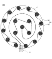
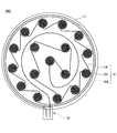
- FIG. 2 is a diagram for explaining an example of the temperature measurement wafer according to the first embodiment.
- the temperature measurement wafer 10 ⁇ / b> A of the first embodiment includes a wafer 11 and an optical fiber 12.
- the wafer 11 for example, a silicon (Si) wafer can be used.
- the diameter of the wafer 11 is not specifically limited, For example, it can be 300 mm and 450 mm.
- the optical fiber 12 is laid on the surface of the wafer 11.
- the optical fiber 12 is a single thin fiber tube made of quartz glass, plastic or the like. Pulse light output from the light source 31 illustrated in FIG. 1 is incident on the optical fiber 12.
- the optical fiber 12 has a starting end and a terminating end on the outer peripheral portion of the wafer 11.
- the start end and the end end function as a connection portion 13 connected to the measuring instrument main body 30 illustrated in FIG. Note that the start end and the end end are only required to allow light to enter, and may be arranged at the center of the wafer 11, for example.
- the optical fiber 12 has a sparsely formed part (hereinafter referred to as “sparse part 14”) and a part formed more densely than the sparse part 14 (hereinafter referred to as “dense part 15”) between the start end and the terminal end. And).
- the sparse part 14 and the dense part 15 of the optical fiber 12 are alternately arranged.
- the number of sparse portions 14 and the number of dense portions 15 are not particularly limited, but can be determined according to the size of the wafer 11 and the like.
- the dense portions 15 may have the same shape or different shapes.
- FIG. 2 shows an example in which 18 sparse portions 14 and 17 dense portions 15 are alternately arranged over the entire surface of the wafer 11.
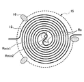
- FIG. 3A and 3B are diagrams illustrating an example of a dense portion of the temperature measurement wafer in FIG. 3A is a schematic plan view of the dense portion, and FIG. 3B is a schematic sectional view of the dense portion. 3A and 3B show one of a plurality of dense portions in the temperature measurement wafer of FIG.
- the dense portion 15 is formed in a spiral shape with the center of the dense portion 15 as the center of the vortex in plan view.
- the number of turns of the dense portion 15 is not particularly limited, but is preferably determined according to the pulse length of the pulsed light incident on the optical fiber 12. This is because in the temperature measurement by the ROTDR system, the spatial resolution in the length direction of the optical fiber 12 depends on the pulse length of the laser light used for the measurement in the core of the optical fiber 12. Specifically, the number of turns is preferably such that the length is equal to or longer than the pulse length of the pulsed light incident on the optical fiber 12. Thereby, the temperature distribution can be measured with a particularly high spatial resolution.
- the number of turns of the dense portion 15 is preferably such that the number of turns is not more than twice the pulse length of the pulsed light incident on the optical fiber 12, and the pulse length of the pulsed light incident on the optical fiber 12 It is more preferable that the number of windings is 1.5 times or less the length. As a result, as many dense portions 15 as possible can be formed on the surface of the wafer 11, the number of measurement points on the surface of the wafer 11 can be increased, and the spatial resolution is improved.
- pulse length L (m) is a value calculated by the following equation (1).
- L c ⁇ t / (2 ⁇ n ⁇ ) (1)
- t (s) is the laser pulse width
- c (m / s) is the speed of light
- ⁇ (nm) is the laser wavelength at the core
- n ⁇ is the refractive index at the laser wavelength ⁇ (nm).
- the pulse length L (m) is about 1 to 2 m.
- the bending radius at the portion where the bending radius of the optical fiber 12 is the smallest is preferably equal to or larger than the allowable bending radius of the optical fiber 12. Is more preferably equal.
- the optical fiber 12 can be laid densely without damaging the optical fiber 12. For this reason, an area required in order to form the same winding number can be made small. As a result, the temperature of a smaller region on the surface of the wafer 11 can be measured. Further, many dense portions 15 can be formed on the surface of the wafer 11, and the spatial resolution when measuring the temperature distribution is improved.
- the minimum bending radius is indicated by Rmin
- the allowable bending radius is indicated by Ra.
- the dense portion 15 is fixed to the surface of the wafer 11 by adhesive members 16 provided at three locations on the outer peripheral portion of the dense portion 15. Thereby, the dense portion 15 can maintain a state in contact with the surface of the wafer 11. For this reason, even in a vacuum, the temperature distribution of the wafer 11 can be measured as in the atmosphere.
- the type of the adhesive member 16 is not particularly limited as long as the dense portion 15 can be fixed to the surface of the wafer 11.
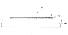
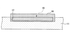
- FIG. 4A and 4B are diagrams showing another example of the dense portion of the temperature measurement wafer shown in FIG. 2, showing a cross section of the dense portion of the temperature measurement wafer.
- the dense portion 15 may be configured to be fixed to the wafer 11 by an adhesive member 16 provided between the wafer 11 and the dense portion 15.
- the adhesive member 16 is preferably a highly heat conductive material, and for example, a heat conductive adhesive or a heat conductive sheet can be used. Thereby, the heat of the wafer 11 can be efficiently transmitted to the dense portion 15. For this reason, even in a vacuum, the temperature distribution of the wafer 11 can be measured as in the atmosphere.
- the dense portion 15 may be disposed in the concave portion 17 formed on the surface of the wafer 11 and covered with the adhesive member 16.
- the adhesive member 16 is preferably a highly heat conductive material, and for example, a heat conductive adhesive or a heat conductive sheet can be used. Thereby, the heat of the wafer 11 can be efficiently transmitted to the dense portion 15. For this reason, even in a vacuum, the temperature distribution of the wafer 11 can be measured as in the atmosphere.
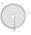
- FIG. 5 is a view showing still another example of the dense portion of the temperature measurement wafer in FIG. 2, and shows the upper surface of the dense portion of the temperature measurement wafer.
- the dense portion 15 has two centers in plan view, and the midpoint of the entire length of the optical fiber 12 laid in the area of the dense portion 15 is located at the center of the dense portion 15. It is formed in a spiral shape.
- the number of turns of the dense portion 15 is not particularly limited, but is preferably such that the number of turns is equal to or longer than the pulse length of the pulsed light incident on the optical fiber 12. Thereby, the temperature distribution can be measured with a particularly high spatial resolution.
- the number of turns of the dense portion 15 is preferably such that the number of turns is not more than twice the pulse length of the pulsed light incident on the optical fiber 12, and the pulse length of the pulsed light incident on the optical fiber 12 It is more preferable that the number of windings is 1.5 times or less the length. As a result, as many dense portions 15 as possible can be formed on the surface of the wafer 11, so that the spatial resolution is improved.
- the minimum bending radius of the optical fiber 12 is preferably equal to or larger than the allowable bending radius of the optical fiber 12, and more preferably equal to the allowable bending radius.
- the optical fiber 12 can be laid densely without damaging the optical fiber 12. For this reason, an area required in order to form the same winding number can be made small. As a result, the temperature of a smaller region on the surface of the wafer 11 can be measured. Further, many dense portions 15 can be formed on the surface of the wafer 11, and the spatial resolution when measuring the temperature distribution is improved.
- the minimum bending radii are indicated by Rmin1 and Rmin2, and the allowable bending radius is indicated by Ra.
- the optical fiber 12 and the adhesive member 16 are only provided on the surface of the wafer 11. For this reason, the cost for manufacturing the temperature measurement wafer 10A can be reduced. In addition, since no electrical element is included, the temperature distribution can be measured without being affected by electromagnetic noise due to plasma, for example, even in the environment of a substrate processing apparatus where plasma is generated.
- the dense portions 15 can be easily viewed and the temperature measurement position is identified. The temperature at a desired position of the wafer 11 can be measured.
- FIG. 6 is a diagram for explaining an example of a temperature measurement wafer according to the second embodiment.
- the temperature measurement wafer 10 ⁇ / b> B of the second embodiment includes a wafer 11 and an optical fiber 12.
- the wafer 11 for example, a silicon (Si) wafer can be used.
- the diameter of the wafer 11 is not specifically limited, For example, it can be 300 mm and 450 mm.
- the optical fiber 12 is laid on the surface of the wafer 11.
- the optical fiber 12 is a single thin fiber tube made of quartz glass, plastic or the like. Pulse light output from the light source 31 illustrated in FIG. 1 is incident on the optical fiber 12.
- the optical fiber 12 has a starting end and a terminating end on the outer peripheral portion of the wafer 11.
- the start end and the end end function as a connection portion 13 connected to the measuring instrument main body 30 illustrated in FIG. Note that the start end and the end end are only required to allow light to enter, and may be arranged at the center of the wafer 11, for example.
- the optical fiber 12 is arranged between the starting end and the terminal end, the dense portion 15 disposed on the outer peripheral portion of the wafer 11, the central portion of the wafer 11 with respect to the dense portion 15, and sparser than the dense portion 15. And a sparse part 14.
- the number of turns of the dense portion 15 is not particularly limited, but is preferably such that the number of turns is equal to or longer than the pulse length of the pulsed light incident on the optical fiber 12. Thereby, the temperature distribution can be measured with a particularly high spatial resolution.
- the number of turns of the dense portion 15 is preferably such that the number of turns is not more than twice the pulse length of the pulsed light incident on the optical fiber 12, and the pulse length of the pulsed light incident on the optical fiber 12 It is more preferable that the number of windings is 1.5 times or less the length. As a result, as many dense portions 15 as possible can be formed on the surface of the wafer 11, so that the spatial resolution is improved.
- FIG. 6 shows an example in which one sparse part 14 and one dense part 15 are arranged, but the dense part 15 and the sparse part 14 are alternately arranged from the outer peripheral part of the wafer 11 toward the center. It may be arranged. Since the dense portions 15 and the sparse portions 14 are alternately arranged from the outer peripheral portion of the wafer 11 toward the center, the spatial resolution in the radial direction of the wafer 11 can be particularly improved. Further, when the dense portions 15 and the sparse portions 14 are alternately arranged from the outer peripheral portion to the center of the wafer 11, the dense portions 15 can be easily viewed, the temperature measurement position can be easily identified, and the wafer 11. The temperature at a desired position in the radial direction can be measured.
- the sparse part 14 and the dense part arranged more densely than the sparse part 14 on the surface of the wafer 11, as in the first embodiment. 15 is laid.
- the optical fiber 12 and the adhesive member 16 are only provided on the surface of the wafer 11, as in the first embodiment. For this reason, the cost for manufacturing the temperature measurement wafer 10B can be reduced. In addition, since no electrical element is included, the temperature distribution can be measured without being affected by electromagnetic noise due to plasma, for example, even in the environment of a substrate processing apparatus where plasma is generated.
- the dense portion 15 is disposed on the outer peripheral portion of the wafer 11 and the sparse portion 14 is disposed closer to the center of the wafer 11 than the dense portion 15, thereby improving the spatial resolution of the outer peripheral portion.
- the spatial resolution in the radial direction of the wafer 11 can be improved.
- FIG. 7 is a diagram for explaining an example of a temperature measurement wafer according to the third embodiment.
- the temperature measurement wafer 10 ⁇ / b> C of the third embodiment includes a wafer 11 and an optical fiber 12.
- the wafer 11 for example, a silicon (Si) wafer can be used.
- the diameter of the wafer 11 is not specifically limited, For example, it can be 300 mm and 450 mm.
- the optical fiber 12 is laid on the surface of the wafer 11.
- the optical fiber 12 is a single thin fiber tube made of quartz glass, plastic or the like. Pulse light output from the light source 31 illustrated in FIG. 1 is incident on the optical fiber 12.
- the optical fiber 12 has a starting end and a terminating end on the outer peripheral portion of the wafer 11.
- the start end and the end end function as a connection portion 13 connected to the measuring instrument main body 30 illustrated in FIG. Note that the start end and the end end are only required to allow light to enter, and may be arranged at the center of the wafer 11, for example.
- the optical fiber 12 includes a first dense portion 151 disposed on the outer peripheral portion of the wafer 11 between a start end and a terminal end, and a second dense portion 151 disposed closer to the center of the wafer 11 than the first dense portion 151.
- the dense portion 152 and the sparse portion 14 are included.
- the first dense portion 151 can have the same configuration as the dense portion 15 of the second embodiment, and the sparse portion 14 and the second dense portion 152 are the sparse portion 14 and the dense portion 15 of the first embodiment. It can be set as the same structure.
- the sparse part 14 and the second sparse part 14 are arranged more densely on the surface of the wafer 11 as in the first embodiment.
- the optical fiber 12 having the dense portion 152 and the first dense portion 151 disposed on the outer peripheral portion of the wafer 11 is laid as in the second embodiment.
- the optical fiber 12 and the adhesive member 16 are only provided on the surface of the wafer 11. For this reason, the cost for manufacturing the temperature measurement wafer 10 ⁇ / b> C can be reduced. In addition, since no electrical element is included, the temperature distribution can be measured without being affected by electromagnetic noise due to plasma, for example, even in the environment of a substrate processing apparatus where plasma is generated.
- a plurality of second dense portions 152 and sparse portions 14 are alternately arranged on the surface of the wafer 11 as in the first embodiment.
- the in-plane temperature distribution can be measured finely with high spatial resolution over the entire 11 surfaces.
- the first dense portion 151 is arranged on the outer peripheral portion of the wafer 11 as in the second embodiment, and the center of the wafer 11 is located more than the first dense portion 151. Since the sparse part 14 is arranged on the side, the spatial resolution of the outer peripheral part can be improved and the spatial resolution in the radial direction of the wafer 11 can be improved. As described above, in the third embodiment, it is possible to finely measure the in-plane temperature distribution with high spatial resolution on the entire surface of the wafer 11 by using the single temperature measurement wafer 10C, and the outer peripheral portion and the radial direction of the wafer 11 can be measured. It is possible to improve the spatial resolution. Therefore, it is not necessary to measure the temperature distribution of the wafer 11 using a plurality of temperature measurement wafers, and the time for measuring the temperature distribution of the wafer 11 can be shortened.
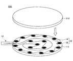
- FIGS. 8A and 8B are diagrams for explaining an example of the temperature measurement wafer according to the fourth embodiment.
- 8A is a schematic perspective view of the temperature measurement wafer
- FIG. 8B is an exploded perspective view of the temperature measurement wafer of FIG. 8A.
- the temperature measurement wafer 10D of the fourth embodiment includes a first wafer 111, a second wafer 112, and an optical fiber laying portion 18.
- the optical fiber laying portion 18 is formed by bonding the second wafer 112 to the surface of the first wafer 111 on the side where the optical fiber 12 is laid using an unillustrated adhesive member. Is formed. That is, the optical fiber 12 is sandwiched between the first wafer 111 and the second wafer 112, and a gap between the first wafer 111 and the second wafer 112 is filled with an adhesive member.
- the optical fiber 12 includes a sparse portion 14 and a dense portion 15 formed more densely than the sparse portion 14 between the start end and the end.
- the parts 15 are arranged alternately.
- the optical fiber 12 may be arrange
- the optical fiber 12 is sandwiched between the first wafer 111 and the second wafer 112, and is bonded to the gap between the first wafer 111 and the second wafer 112. Since the member is filled, the optical fiber 12 is not exposed. For this reason, the optical fiber 12 is not directly exposed to the process environment, and deterioration of the surface of the optical fiber 12 due to corrosive gas or plasma can be suppressed. As a result, the durability of the temperature measuring wafer 10D is improved.
- the temperature measurement wafer 10 is an example of a temperature measurement substrate.
- the wafer 11 is an example of a substrate.
- the sparse part 14 is an example of a first pattern part.
- the dense portion 15 is an example of a second pattern portion.
- the optical fiber 12 is laid on one surface of the wafer 11 has been described as an example.
- the optical fiber 12 may be laid on both surfaces of the wafer 11. .
- the temperature measurement wafer 10 in each of the above embodiments may be used in a state where it is mounted on a wafer mounting table that holds the wafer, for example, in order to perform predetermined processing or inspection on the wafer.
- the temperature measurement wafer 10 is used while being mounted on the wafer mounting table, when the optical fiber 12 is laid on one surface of the wafer 11, for example, one surface of the wafer 11 is placed on the upper side.
- the fiber 12 may be placed without contacting the wafer placement table.
- the optical fiber 12 may be placed in a state of contacting the wafer placing table with one surface of the wafer 11 being the lower side.
- the substrate used for the temperature measurement substrate of the present invention is not limited to a wafer, and may be a substrate used for a flat panel display or a solar cell, for example.
Landscapes
- Physics & Mathematics (AREA)
- General Physics & Mathematics (AREA)
- Measuring Temperature Or Quantity Of Heat (AREA)
Abstract
Description
本実施形態の温度測定システムについて説明する。本実施形態の温度測定システムは、半導体ウエハ(以下「ウエハ」という。)の表面に敷設した光ファイバをセンサとして用い、後方散乱光の一つであるラマン散乱光を利用して光ファイバに沿った温度分布を測定するシステムである。本実施形態の温度測定システムは、例えば半導体ウエハ等の基板に対し、熱処理等の所定の処理を施す基板処理装置に用いられる。以下では、後方散乱光の一つであるラマン散乱光を利用して光ファイバに沿った温度分布を測定するシステムをROTDR(Raman Optical Time Domain Reflectometer)システムとも称する。
本実施形態の温度測定用ウエハ10について説明する。本実施形態の温度測定用ウエハ10は、ウエハの表面に敷設された光ファイバ内にパルス光を入射させてウエハの温度分布を算出する際に用いられる。以下では、ウエハの温度分布を測定可能な、第1実施形態から第4実施形態の温度測定用ウエハについて説明する。
図2は、第1実施形態の温度測定用ウエハの一例を説明するための図である。
ここで、t(s)はレーザのパルス幅、c(m/s)は光速、λ(nm)はコアにおけるレーザ波長、nλはレーザ波長λ(nm)における屈折率である。なお、一般的なROTDRシステムを用いる場合、パルス長L(m)は1~2m程度である。
図6は、第2実施形態の温度測定用ウエハの一例を説明するための図である。
図7は、第3実施形態の温度測定用ウエハの一例を説明するための図である。
図8A及び図8Bは、第4実施形態の温度測定用ウエハの一例を説明するための図である。図8Aは温度測定用ウエハの概略斜視図であり、図8Bは図8Aの温度測定用ウエハの分解斜視図である。
11 ウエハ
12 光ファイバ
13 接続部
14 疎部
15 密部
16 接着部材
17 凹部
18 光ファイバ敷設部
20 計算機
30 計測機本体
Claims (15)
- 半導体ウエハ、又はフラットパネルディスプレイ用基板のいずれかである基板と、
前記基板の表面に敷設され、第1のパターン部と、前記第1のパターン部よりも密に形成された第2のパターン部とを有する、少なくとも1本の光ファイバと、
を備える、温度測定用基板。 - 前記光ファイバは、光を入射可能な始端及び終端を有する、
請求項1に記載の温度測定用基板。 - 前記第1のパターン部と前記第2のパターン部とが交互に配置されている、
請求項1に記載の温度測定用基板。 - 前記第2のパターン部の長さは、前記光ファイバに入射するパルス光のパルス長以上である、
請求項1に記載の温度測定用基板。 - 前記第2のパターン部は、平面視で渦巻き状に形成されている、
請求項1に記載の温度測定用基板。 - 前記第2のパターン部の最小曲げ半径は、前記光ファイバの許容曲げ半径以上である、
請求項1に記載の温度測定用基板。 - 前記第2のパターン部の最小曲げ半径は、前記光ファイバの許容曲げ半径と等しい、
請求項1に記載の温度測定用基板。 - 前記光ファイバは、複数の前記第2のパターン部を有し、
前記複数の第2のパターン部のそれぞれが同一の形状である、
請求項1に記載の温度測定用基板。 - 前記第2のパターン部は、前記基板の外周部に配置されており、
前記第1のパターン部は、前記第2のパターン部よりも前記基板の中心側に配置されている、
請求項1に記載の温度測定用基板。 - 前記第2のパターン部は、平面視で渦巻き状に形成された部分と、前記第1のパターン部よりも外周側に配置された部分とを有する、
請求項1に記載の温度測定用基板。 - 前記第2のパターン部は、接着部材により前記基板の表面に固定されている、
請求項1に記載の温度測定用基板。 - 前記第2のパターン部は、前記接着部材に覆われている、
請求項11に記載の温度測定用基板。 - 前記接着部材は、高熱伝導性材料である、
請求項11に記載の温度測定用基板。 - 前記基板は、半導体ウエハである、
請求項1に記載の温度測定用基板。 - 請求項1に記載の温度測定用基板と、
前記温度測定用基板の前記光ファイバにパルス光を入射させる計測機本体と、
を備える、
温度測定システム。
Priority Applications (4)
| Application Number | Priority Date | Filing Date | Title |
|---|---|---|---|
| JP2018513105A JP6694503B2 (ja) | 2016-04-19 | 2017-04-06 | 温度測定用基板及び温度測定システム |
| KR1020187029883A KR102414892B1 (ko) | 2016-04-19 | 2017-04-06 | 온도 측정용 기판 및 온도 측정 시스템 |
| US16/095,114 US11035741B2 (en) | 2016-04-19 | 2017-04-06 | Temperature measurement substrate and temperature measurement system |
| CN201780002554.7A CN107850495B (zh) | 2016-04-19 | 2017-04-06 | 温度测量用基板以及温度测量系统 |
Applications Claiming Priority (2)
| Application Number | Priority Date | Filing Date | Title |
|---|---|---|---|
| JP2016-083933 | 2016-04-19 | ||
| JP2016083933 | 2016-04-19 |
Publications (1)
| Publication Number | Publication Date |
|---|---|
| WO2017183471A1 true WO2017183471A1 (ja) | 2017-10-26 |
Family
ID=60115945
Family Applications (1)
| Application Number | Title | Priority Date | Filing Date |
|---|---|---|---|
| PCT/JP2017/014374 Ceased WO2017183471A1 (ja) | 2016-04-19 | 2017-04-06 | 温度測定用基板及び温度測定システム |
Country Status (6)
| Country | Link |
|---|---|
| US (1) | US11035741B2 (ja) |
| JP (1) | JP6694503B2 (ja) |
| KR (1) | KR102414892B1 (ja) |
| CN (1) | CN107850495B (ja) |
| TW (1) | TWI718285B (ja) |
| WO (1) | WO2017183471A1 (ja) |
Cited By (5)
| Publication number | Priority date | Publication date | Assignee | Title |
|---|---|---|---|---|
| WO2020013299A1 (ja) * | 2018-07-12 | 2020-01-16 | 東京エレクトロン株式会社 | 温度測定センサ、温度測定システム、および、温度測定方法 |
| TWI705234B (zh) * | 2017-12-05 | 2020-09-21 | 法商歐洲雷射系統與方案解決公司 | 用於測量基板的表面溫度之裝置及方法 |
| US20220244111A1 (en) * | 2021-02-01 | 2022-08-04 | Fuji Electric Co., Ltd. | Semiconductor device and temperature measurement method |
| WO2023164415A1 (en) * | 2022-02-22 | 2023-08-31 | Lam Research Corporation | Sensors for semiconductor processing tools |
| JP2024019821A (ja) * | 2022-08-01 | 2024-02-14 | 三星電子株式会社 | 光ファイバー式ウェハー温度センサー、ウェハー温度計測センサーシステム及びウェハー温度計測センサーの製造方法 |
Families Citing this family (3)
| Publication number | Priority date | Publication date | Assignee | Title |
|---|---|---|---|---|
| KR102288155B1 (ko) * | 2019-08-13 | 2021-08-10 | 한국광기술원 | 온도 센서 및 그를 포함하는 온도 센싱 시스템 |
| US11808663B2 (en) * | 2021-06-09 | 2023-11-07 | Saudi Arabian Oil Company | In situ leakage detection system for buried nonmetallic pipeline |
| KR102364685B1 (ko) * | 2021-09-09 | 2022-02-18 | (주)바이컴 | Dts 기반의 과열 모니터링 장치 |
Citations (3)
| Publication number | Priority date | Publication date | Assignee | Title |
|---|---|---|---|---|
| JP2002544502A (ja) * | 1999-05-10 | 2002-12-24 | センサーレイ コーポレイション | 集積回路製造ツール基板上で温度を検出する装置 |
| JP2011529400A (ja) * | 2008-07-31 | 2011-12-08 | エス・エム・エス・ジーマーク・アクチエンゲゼルシャフト | 繊維光学的測定方法による金型のメニスカスの測定 |
| WO2015025808A1 (ja) * | 2013-08-19 | 2015-02-26 | 株式会社ニコン | ファイバの固定方法、ファイバ保持部材に固定されたファイバ固定構造体、該ファイバ固定構造体を備えたレーザ装置、露光装置及び検査装置 |
Family Cites Families (24)
| Publication number | Priority date | Publication date | Assignee | Title |
|---|---|---|---|---|
| JPH05346355A (ja) | 1992-06-16 | 1993-12-27 | Toshiba Corp | 光ファイバ温度分布センサ装置 |
| JPH06123659A (ja) * | 1992-10-12 | 1994-05-06 | Furukawa Electric Co Ltd:The | 光ファイバ温度センサ |
| US5775808A (en) * | 1996-06-19 | 1998-07-07 | Applied Materials, Inc. | Apparatus for real-time, in situ measurement of temperature and a method of fabricating and using same |
| JP2955930B1 (ja) | 1998-05-29 | 1999-10-04 | 坂口電熱株式会社 | 温度検出素子を有するウェーハ |
| JP2002071323A (ja) * | 2000-08-29 | 2002-03-08 | Mitsubishi Cable Ind Ltd | 面状センサ |
| JP2002169029A (ja) * | 2000-12-01 | 2002-06-14 | Mitsubishi Electric Corp | 光分散等化器 |
| KR20040054177A (ko) * | 2002-12-18 | 2004-06-25 | 엘지전선 주식회사 | 분포온도 측정 장치의 표준 온도 및 거리 측정 장치 |
| US20040136681A1 (en) * | 2003-01-10 | 2004-07-15 | Novellus Systems, Inc. | Erbium-doped oxide glass |
| US6915589B2 (en) * | 2003-10-16 | 2005-07-12 | Sensarray Corporation | Sensor positioning systems and methods |
| JP2005195502A (ja) * | 2004-01-08 | 2005-07-21 | Occ Techno Ltd | 光ファイバ型温度計測装置及び温度計測方法 |
| JP2006177780A (ja) * | 2004-12-22 | 2006-07-06 | Hitachi Cable Ltd | 光ファイバ温度センサ、温度センサシート及び温度測定方法 |
| CN101155662B (zh) * | 2005-04-01 | 2010-09-01 | 通快机床两合公司 | 包括以像素矩阵形式提供的温度传感器的光学元件及记录射束参数的方法 |
| US7543981B2 (en) * | 2006-06-29 | 2009-06-09 | Mattson Technology, Inc. | Methods for determining wafer temperature |
| JP5476114B2 (ja) * | 2009-12-18 | 2014-04-23 | 東京エレクトロン株式会社 | 温度測定用装置 |
| US8740455B2 (en) * | 2010-12-08 | 2014-06-03 | Baker Hughes Incorporated | System and method for distributed environmental parameter measurement |
| DE102011116243B4 (de) * | 2011-10-17 | 2014-04-17 | Centrotherm Photovoltaics Ag | Vorrichtung zum Bestimmen der Temperatur eines Substrats |
| JP5319856B1 (ja) * | 2012-06-13 | 2013-10-16 | 株式会社シンクロン | 膜厚測定装置及び成膜装置 |
| US9645018B2 (en) * | 2013-02-19 | 2017-05-09 | Chung Lee | Method and apparatus for auto-correcting the distributed temperature sensing system |
| JP6608923B2 (ja) * | 2014-07-02 | 2019-11-20 | アプライド マテリアルズ インコーポレイテッド | 溝に経路指定された光ファイバーによる加熱を含む温度制御装置、基板温度制御システム、電子デバイス処理システム、及び処理方法 |
| TWI603416B (zh) * | 2014-07-08 | 2017-10-21 | 瓦特洛威電子製造公司 | 具有接合層之整合溫度感測技術的接合總成 |
| KR102395901B1 (ko) * | 2015-01-15 | 2022-05-09 | 삼성디스플레이 주식회사 | 압전 디바이스를 포함하는 표시 패널 및 압전 디바이스의 특성 보상 방법 |
| JP7011214B2 (ja) * | 2017-08-31 | 2022-01-26 | 横河電機株式会社 | 光ファイバセンサ測定ユニット |
| CN107748177A (zh) * | 2017-09-25 | 2018-03-02 | 东华大学 | 一种面料红外发射率的测量方法 |
| JP7379038B2 (ja) * | 2018-10-04 | 2023-11-14 | キヤノン株式会社 | インクジェット記録方法、及びインクジェット記録装置 |
-
2017
- 2017-04-06 KR KR1020187029883A patent/KR102414892B1/ko active Active
- 2017-04-06 WO PCT/JP2017/014374 patent/WO2017183471A1/ja not_active Ceased
- 2017-04-06 JP JP2018513105A patent/JP6694503B2/ja active Active
- 2017-04-06 US US16/095,114 patent/US11035741B2/en active Active
- 2017-04-06 CN CN201780002554.7A patent/CN107850495B/zh active Active
- 2017-04-11 TW TW106111992A patent/TWI718285B/zh active
Patent Citations (3)
| Publication number | Priority date | Publication date | Assignee | Title |
|---|---|---|---|---|
| JP2002544502A (ja) * | 1999-05-10 | 2002-12-24 | センサーレイ コーポレイション | 集積回路製造ツール基板上で温度を検出する装置 |
| JP2011529400A (ja) * | 2008-07-31 | 2011-12-08 | エス・エム・エス・ジーマーク・アクチエンゲゼルシャフト | 繊維光学的測定方法による金型のメニスカスの測定 |
| WO2015025808A1 (ja) * | 2013-08-19 | 2015-02-26 | 株式会社ニコン | ファイバの固定方法、ファイバ保持部材に固定されたファイバ固定構造体、該ファイバ固定構造体を備えたレーザ装置、露光装置及び検査装置 |
Cited By (13)
| Publication number | Priority date | Publication date | Assignee | Title |
|---|---|---|---|---|
| TWI705234B (zh) * | 2017-12-05 | 2020-09-21 | 法商歐洲雷射系統與方案解決公司 | 用於測量基板的表面溫度之裝置及方法 |
| US11841278B2 (en) | 2018-07-12 | 2023-12-12 | Tokyo Electron Limited | Temperature measurement sensor, temperature measurement system, and temperature measurement method |
| JP2020008523A (ja) * | 2018-07-12 | 2020-01-16 | 東京エレクトロン株式会社 | 温度測定センサ、温度測定システム、および、温度測定方法 |
| US20200408613A1 (en) * | 2018-07-12 | 2020-12-31 | Tokyo Electron Limited | Temperature measurement sensor, temperature measurement system, and temperature measurement method |
| KR20210029136A (ko) | 2018-07-12 | 2021-03-15 | 도쿄엘렉트론가부시키가이샤 | 온도 측정 센서, 온도 측정 시스템, 및 온도 측정 방법 |
| JP7066557B2 (ja) | 2018-07-12 | 2022-05-13 | 東京エレクトロン株式会社 | 温度測定センサ、温度測定システム、および、温度測定方法 |
| TWI821333B (zh) * | 2018-07-12 | 2023-11-11 | 日商東京威力科創股份有限公司 | 測定感測器、溫度測定系統及測定方法 |
| WO2020013299A1 (ja) * | 2018-07-12 | 2020-01-16 | 東京エレクトロン株式会社 | 温度測定センサ、温度測定システム、および、温度測定方法 |
| KR102821505B1 (ko) * | 2018-07-12 | 2025-06-18 | 도쿄엘렉트론가부시키가이샤 | 온도 측정 센서, 온도 측정 시스템, 및 온도 측정 방법 |
| US20220244111A1 (en) * | 2021-02-01 | 2022-08-04 | Fuji Electric Co., Ltd. | Semiconductor device and temperature measurement method |
| US12163845B2 (en) * | 2021-02-01 | 2024-12-10 | Fuji Electric Co., Ltd. | Semiconductor device and temperature measurement method |
| WO2023164415A1 (en) * | 2022-02-22 | 2023-08-31 | Lam Research Corporation | Sensors for semiconductor processing tools |
| JP2024019821A (ja) * | 2022-08-01 | 2024-02-14 | 三星電子株式会社 | 光ファイバー式ウェハー温度センサー、ウェハー温度計測センサーシステム及びウェハー温度計測センサーの製造方法 |
Also Published As
| Publication number | Publication date |
|---|---|
| US11035741B2 (en) | 2021-06-15 |
| JP6694503B2 (ja) | 2020-05-13 |
| CN107850495B (zh) | 2020-06-30 |
| KR20180133422A (ko) | 2018-12-14 |
| KR102414892B1 (ko) | 2022-07-01 |
| US20190120703A1 (en) | 2019-04-25 |
| TWI718285B (zh) | 2021-02-11 |
| JPWO2017183471A1 (ja) | 2019-02-21 |
| CN107850495A (zh) | 2018-03-27 |
| TW201802441A (zh) | 2018-01-16 |
Similar Documents
| Publication | Publication Date | Title |
|---|---|---|
| JP6694503B2 (ja) | 温度測定用基板及び温度測定システム | |
| CN101542255A (zh) | 光纤式温度计以及温度补偿型光纤传感器 | |
| Zhang et al. | Single-crystal sapphire-based optical high-temperature sensor for harsh environments | |
| CN109374112B (zh) | 光纤二维振动传感器及其制作方法 | |
| KR20130106178A (ko) | 광학적 방법을 이용한 두께 및 형상 측정 장치 및 측정 방법 | |
| JP2022153599A (ja) | 光センサおよびそれを用いた分析装置 | |
| US12196629B2 (en) | Measuring device and optical fiber strain measuring jig thereof | |
| US7286237B2 (en) | Fiber optic sensor | |
| JP2012225729A (ja) | Fbgひずみセンサ | |
| KR101223762B1 (ko) | 표면 플라즈몬 브래그 격자 도파로를 이용한 바이오센서 소자 및 타겟 물질 검출 방법 | |
| Chao et al. | Two optofluidic devices for the refractive index measurement of small volume of fluids | |
| JP2005351663A (ja) | Fbg湿度センサ及びfbg湿度センサを用いた湿度測定方法 | |
| JP5136008B2 (ja) | センサ | |
| JP2010271254A (ja) | 光ファイバ温度測定器 | |
| JP2004205381A (ja) | 微小荷重測定装置 | |
| JP4862594B2 (ja) | 光ファイバセンサ | |
| JP3631221B2 (ja) | ファイバ分光検出器及びその製造方法 | |
| US20260036472A1 (en) | Optical sensing method and optical sensor system for an optical sensing method | |
| Nawrot et al. | Simultaneous Multi-Point Refractive Index Sensing Using FIB-Fabricated D-Shaped Optical Fiber Sensors Interrogated via OTDR | |
| JP2009145308A (ja) | 屈折率センサおよび液位センサ | |
| CN116448007A (zh) | 一种传感探头、曲率传感器及曲率检测方法 | |
| JP2008501119A (ja) | 応力感応素子を有する半導体構造、および半導体構造内の応力を測定するための方法 | |
| Kim et al. | Design and Fabrication of a Novel Noncontact Vibration Sensor Using Inclined-Cut Optical Fiber | |
| JPH0684917B2 (ja) | 圧力センサ | |
| CN117249916A (zh) | 用于检测介质界面温度的系统及方法 |
Legal Events
| Date | Code | Title | Description |
|---|---|---|---|
| ENP | Entry into the national phase |
Ref document number: 2018513105 Country of ref document: JP Kind code of ref document: A |
|
| ENP | Entry into the national phase |
Ref document number: 20187029883 Country of ref document: KR Kind code of ref document: A |
|
| NENP | Non-entry into the national phase |
Ref country code: DE |
|
| 121 | Ep: the epo has been informed by wipo that ep was designated in this application |
Ref document number: 17785813 Country of ref document: EP Kind code of ref document: A1 |
|
| 122 | Ep: pct application non-entry in european phase |
Ref document number: 17785813 Country of ref document: EP Kind code of ref document: A1 |