WO2017175649A1 - 液晶ポリマー片面積層板 - Google Patents
液晶ポリマー片面積層板 Download PDFInfo
- Publication number
- WO2017175649A1 WO2017175649A1 PCT/JP2017/013068 JP2017013068W WO2017175649A1 WO 2017175649 A1 WO2017175649 A1 WO 2017175649A1 JP 2017013068 W JP2017013068 W JP 2017013068W WO 2017175649 A1 WO2017175649 A1 WO 2017175649A1
- Authority
- WO
- WIPO (PCT)
- Prior art keywords
- liquid crystal
- crystal polymer
- thermosetting resin
- layer
- plate according
- Prior art date
- Legal status (The legal status is an assumption and is not a legal conclusion. Google has not performed a legal analysis and makes no representation as to the accuracy of the status listed.)
- Ceased
Links
Images


Classifications
-
- B—PERFORMING OPERATIONS; TRANSPORTING
- B32—LAYERED PRODUCTS
- B32B—LAYERED PRODUCTS, i.e. PRODUCTS BUILT-UP OF STRATA OF FLAT OR NON-FLAT, e.g. CELLULAR OR HONEYCOMB, FORM
- B32B15/00—Layered products comprising a layer of metal
- B32B15/04—Layered products comprising a layer of metal comprising metal as the main or only constituent of a layer, which is next to another layer of the same or of a different material
- B32B15/08—Layered products comprising a layer of metal comprising metal as the main or only constituent of a layer, which is next to another layer of the same or of a different material of synthetic resin
-
- B—PERFORMING OPERATIONS; TRANSPORTING
- B32—LAYERED PRODUCTS
- B32B—LAYERED PRODUCTS, i.e. PRODUCTS BUILT-UP OF STRATA OF FLAT OR NON-FLAT, e.g. CELLULAR OR HONEYCOMB, FORM
- B32B27/00—Layered products comprising a layer of synthetic resin
- B32B27/18—Layered products comprising a layer of synthetic resin characterised by the use of special additives
- B32B27/20—Layered products comprising a layer of synthetic resin characterised by the use of special additives using fillers, pigments, thixotroping agents
-
- H—ELECTRICITY
- H05—ELECTRIC TECHNIQUES NOT OTHERWISE PROVIDED FOR
- H05K—PRINTED CIRCUITS; CASINGS OR CONSTRUCTIONAL DETAILS OF ELECTRIC APPARATUS; MANUFACTURE OF ASSEMBLAGES OF ELECTRICAL COMPONENTS
- H05K1/00—Printed circuits
- H05K1/02—Details
- H05K1/03—Use of materials for the substrate
Definitions
- the present invention is excellent in pressure resistance in addition to heat resistance, and is a liquid crystal polymer single area layer plate to which a mounting method under high pressure such as a wire bonding method or a flip chip bonding method without using solder can be applied, and
- the present invention relates to a multilayer substrate including a liquid crystal polymer single area layer plate and an electronic circuit substrate.
- a prepreg obtained by impregnating a glass nonwoven fabric with an epoxy resin or the like has been used as a substrate material for an electronic circuit board.
- an epoxy resin or the like has been used as a substrate material for an electronic circuit board.
- lightweight and flexible polyimide films have been used as substrate materials for electronic circuit boards.
- Patent Document 1 discloses an IC chip mounting interposer in which a conductor pattern is formed on the surface of a liquid crystal polymer film having heat resistance sufficient for mounting using solder reflow, and the interposer. Discloses an IC chip package in which an IC chip is mounted.
- the liquid crystal polymer film has an advantage that a circuit board capable of high-speed transmission can be configured because of its low dielectric constant and low dielectric loss.
- Patent Document 2 discloses a multilayer printed circuit board in which layers are connected by through-holes, and includes a liquid crystal polymer as a material for a resin film that is an insulating base material or a cover layer.
- the liquid crystal polymer film has a track record of use as an insulating substrate material for circuit boards.
- the metal foil is directly thermocompression-bonded using the thermoplasticity of the liquid crystal polymer, or cracks are suppressed and the interlayer is prevented.
- the adhesive was attached with a deformable adhesive.
- the present invention provides a liquid crystal polymer single area layer plate capable of stably mounting components by a wire bonding method or a flip chip bonding method without using solder, and a mounting reliability obtained by laminating the liquid crystal polymer single area layer plate. It aims at providing a high multilayer substrate.
- the present inventor has conducted extensive research to solve the above problems. As a result, high temperature is applied to solder mounting while no pressure is applied. However, in the above-described improved mounting method, not only high temperature but also pressure is applied to the circuit board, so the metal foil directly heats the liquid crystal polymer film. It has been found that electronic components cannot be stably mounted on a conventional liquid crystal polymer circuit board that is pressure-bonded or attached via an adhesive that is easily deformed.
- a flexible insulating base material is used to suppress cracks, and the adhesive layer is naturally acceptable for the same purpose. Should show gender.
- the materials of the insulating base and the adhesive layer exemplified in Patent Document 3 are exactly the same. Therefore, the conductor pad provided on the adhesive layer sinks under pressure during mounting by the wire bonding method or the flip chip bonding method without using solder, and the energy required for bonding, such as ultrasonic waves, is generated by the insulating base material or adhesive. In some cases, the mounting itself cannot be performed or the component cannot be mounted at a desired position.
- covers a liquid-crystal polymer film in the insulating film of patent document 4, 5 consists of an organic substance with a low elastic modulus. Since the elastic modulus is a physical property value indicating difficulty in deformation, the liquid crystal polymer insulating films of Patent Documents 4 and 5 cannot be applied to a mounting method in which pressure is applied at a high temperature.
- thermosetting resin cured product layer and a metal foil are provided in this order on one surface of the liquid crystal polymer film,
- the thermosetting resin cured product layer contains an inorganic filler,
- thermosetting resin cured product layer further contains a black filler.
- thermosetting resin cured product layer is 5 ⁇ m or more and 50 ⁇ m or less.
- a multilayer substrate having a circuit of two or more layers, having the liquid crystal polymer single area layer plate according to any one of the above [1] to [10] at the uppermost portion, and the metal foil side thereof being positioned on the upper side A multilayer substrate characterized by that.
- the liquid crystal polymer single-area layer plate according to the present invention is excellent not only in heat resistance but also in pressure resistance. Therefore, it is possible to apply a mounting method in which pressure and ultrasonic waves are loaded in addition to high temperature, such as a wire bonding method and a flip chip bonding method without using solder.
- the liquid crystal polymer film has excellent dielectric properties and is easily thermoplastic because of its thermoplasticity.
- contact failure is likely to occur, the yield is reduced, and only an electronic circuit board with low reliability is obtained.
- the liquid crystal polymer single-area layer plate according to the present invention is excellent in pressure resistance and the like while including a liquid crystal polymer film, and a highly reliable electronic circuit board can be obtained even when the above improved mounting method is applied. In this respect, the industrial significance is very large.
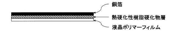
- FIG. 1 is a schematic diagram showing a basic structure of a liquid crystal polymer single area layer plate according to the present invention.
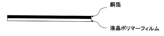
- FIG. 2 is a schematic view showing a basic structure of a conventional liquid crystal polymer two-layer laminate.
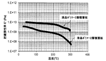
- FIG. 3 is a graph showing the evaluation results of the storage elastic modulus of the liquid crystal polymer single area layer plate.
- FIG. 4 is a schematic diagram showing conditions for a mountability evaluation test of a liquid crystal polymer piece area layer plate.
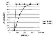
- FIG. 5 is a graph showing the success rate of formation of gold bumps on the conductor pads formed on the copper foil of the liquid crystal polymer single area layer plate.
- FIG. 6 is a graph showing the shear strength of gold bumps formed on the liquid crystal polymer single area layer plate.
- the liquid crystal polymer single area layer plate according to the present invention has a thermosetting resin cured product layer and a metal foil in this order on one surface of the liquid crystal polymer film.
- the liquid crystal polymer includes a thermotropic liquid crystal polymer exhibiting liquid crystallinity in a molten state and a rheotropic liquid crystal polymer exhibiting liquid crystallinity in a solution state.
- a thermotropic liquid crystal polymer is preferably used because it is thermoplastic and is superior in high-frequency characteristics.
- thermotropic liquid crystal polyester (hereinafter simply referred to as “liquid crystal polyester”) is, for example, an aromatic hydroxycarboxylic acid as an essential monomer and reacted with a monomer such as an aromatic dicarboxylic acid or aromatic diol. It is an aromatic polyester obtained by this, and exhibits liquid crystallinity when melted.
- Typical examples thereof include Type I [Formula (1)] synthesized from parahydroxybenzoic acid (PHB), phthalic acid, and 4,4′-biphenol, PHB and 2,6-hydroxynaphthoic acid.
- type I liquid crystal polyester and type II liquid crystal polyester are preferable because they are superior in heat resistance and hydrolysis resistance.
- isophthalic acid is preferable as phthalic acid.
- the thickness of the liquid crystal polymer film in the present invention may be appropriately adjusted, but is preferably 5 ⁇ m or more and 130 ⁇ m or less. If the said thickness is 5 micrometers or more, sufficient intensity
- the liquid crystal polymer film used in the present invention is preferably substantially composed only of a liquid crystal polymer due to dielectric properties and the like, but the liquid crystal polymer exhibits strong anisotropy when subjected to shear stress.
- an alignment relaxation filler for example, the extruded liquid crystal polymer surface becomes smooth, and uniform orientation can be easily obtained.
- a colored filler may be added.
- fillers are roughly classified into inorganic fillers and organic fillers.
- the alignment relaxation or colored filler that may be blended in the liquid crystal polymer film is not particularly limited.
- the shape of the filler is not particularly limited, and examples thereof include a spherical shape, a plate shape, a rod shape, a needle shape, and an indefinite shape, and the size of the filler is preferably 50 nm or more and 10 ⁇ m or less.
- the size of the filler may be measured by measuring the longest part of each filler in the enlarged photograph, or may be a volume average particle diameter or a number average particle diameter obtained from particle size distribution measurement.
- the ratio of the filler to the entire liquid crystal polymer film (total of the liquid crystal polymer and filler) is 20% by mass or less. It is preferable that By making the said ratio 20 mass% or less, the dielectric characteristic of a liquid crystal polymer film can be made excellent.
- the liquid crystal polymer film has a pale yellowish white color, and it is difficult to recognize the circuit pattern because it easily reflects light during AOI inspection (Automated Optical Inspection) to inspect the pattern shape of the electronic circuit board.
- AOI inspection Automated Optical Inspection
- the reflection of light from the liquid crystal polymer film becomes a problem in this way, the reflection of light can be suppressed by adding a black filler.
- the type of black filler is not particularly limited and may be appropriately selected.
- carbon black filler such as carbon black or graphite; triiron tetroxide, Cu—Cr composite oxide, Cu—Cr—Zn composite oxide
- Metal oxide black fillers such as; metal black fillers such as black interference aluminum pigments.
- a carbon black filler from the viewpoints of not excessively deteriorating the dielectric properties of the liquid crystal polymer, light absorption rate and availability, and less residue when drilling during substrate processing. It is more preferable to use carbon black. However, other black fillers can be used as long as they have dielectric properties equivalent to those of carbon black.
- the lightness (L value) of the black liquid crystal polymer film to which a black filler is added for the purpose of suppressing light reflection is preferably 10 or more and 30 or less.
- the addition amount of carbon black should be 0.1% by mass or more and 1.0% by mass or less with respect to the liquid crystal polymer in order to satisfy the above brightness range and not to excessively impair the dielectric properties and insulation. Is preferred. When adding a black filler, you may use another filler together.
- the film extruded from the extruder is strongly oriented in the extrusion direction (MD).
- the film extruded from the extruder is uniaxially stretched only in the direction (TD) perpendicular to the extrusion direction, or biaxially stretched in MD and TD and the stretching ratio in TD is increased.
- the anisotropy of the liquid crystal polymer molecules is reduced to make the film isotropic.
- the thermal linear expansion coefficient in the plane direction of the liquid crystal polymer film is preferably 3 ppm / ° C. or more and 30 ppm / ° C. or less, and the thermal linear expansion coefficient in one direction of the plane direction and the thermal linear expansion coefficient in the direction orthogonal to the direction are
- the ratio is preferably 0.4 or more and 2.5 or less.
- the warpage rate of a laminated plate in which a metal foil is laminated on one side of a liquid crystal polymer film is suppressed to 10% or less.
- the “warp rate” can be obtained in accordance with JIS C6481. Specifically, the film is placed on a horizontal table so that the center of the film is in contact with the table and the four corners are lifted from the table, the distance between the four corners and the table is measured, and the maximum value is obtained. The percentage value divided by the length of the side of the film. Further, when measuring the thermal expansion coefficient in the planar direction, if the difference between the thermal linear expansion coefficient of each of the liquid crystal polymer film MD and TD and the thermal linear expansion coefficient of the metal foil is large, the laminated plate tends to warp.
- the thermal linear expansion coefficient can be measured by a thermomechanical analysis method (TMA method).
- TMA method thermomechanical analysis method
- Q400 manufactured by TA Instruments Inc.
- the sample shape is 4 mm wide
- the distance between chucks is 15 mm
- a load of 0.1 N is applied to a temperature of 170 ° C.
- the temperature is raised from 170 ° C. to room temperature at a temperature drop rate of 10 ° C./min
- the chuck-to-chuck distance between 100 ° C. and 50 ° C. is raised.
- the coefficient of thermal expansion is measured from the change.
- the liquid crystal polymer film is generally excellent in heat resistance, hydrolysis resistance, low moisture absorption, etc., and the liquid crystal polymer film used in the present invention also has these characteristics. Specific criteria for these characteristics are not particularly limited. For example, regarding heat resistance, it is preferable not to be thermally deformed when held at 260 ° C. for 2 minutes, and it is preferable that heat deformation is not caused when held at 280 ° C. for 2 minutes. preferable.
- Hydrolysis resistance can be evaluated by a pressure cooker test (PCT). Specifically, after forming a copper foil pattern having a width of 5 mm on the liquid crystal polymer film and leaving it in an environment of 121 ° C., 2 atm, and 100% RH, the copper foil pattern was adjusted to 50 mm / min using a tensile tester. The peel strength (unit: N / mm) when peeled in the 90 ° direction or 180 ° direction at a speed is measured, and the measured value before and after the treatment is compared, and the strength retention is 50% or more. Can be evaluated in time.
- the liquid crystal polymer film used in the present invention preferably has a hydrolysis resistance of 100 hours or more measured under the above conditions.
- the water absorption rate may be measured according to JIS C6481. Specifically, the weight increase after the liquid crystal polymer film is immersed in water at 23 ° C. for 24 hours is measured as a percentage.
- the liquid crystal polymer film used in the present invention preferably has a water absorption of 0.1% or less, more preferably 0.05% or less, measured under the above conditions.
- the liquid crystal polymer film used in the present invention is preferably excellent in dimensional stability.
- Dimensional stability can be expressed as a dimensional change rate. Specifically, in accordance with JIS C6471, after a metal foil was bonded to a liquid crystal polymer film, the metal foil was completely etched using an aqueous ferric chloride solution, washed with water and dried at 80 ° C. for 30 minutes, The percentage change before and after etching and drying is shown as a percentage.
- the dimensional change rate of the liquid crystal polymer film used in the present invention is preferably from ⁇ 0.1% to 0.1%.
- the dielectric properties of the liquid crystal polymer film are generally excellent.
- the relative dielectric constant and dielectric loss tangent are measured at a frequency of 3 GHz
- the relative dielectric constant of the liquid crystal polymer film used in the present invention is preferably 3.5 or less
- the dielectric loss tangent is preferably 0.003 or less.
- the production method of the liquid crystal polymer film used in the present invention is not particularly limited, and can be produced, for example, by a melt extrusion molding method. Specifically, the melt of the liquid crystal polymer is directly formed into a film by a conventionally known method such as a T-die method or an inflation method. However, when a liquid crystal polymer is formed into a film by the T-die method, rigid liquid crystal polymer molecules are oriented in MD, and the film exhibits anisotropy. In such a case, the anisotropic liquid crystal polymer film is subjected to equal orientation treatment, for example, as in the invention described in JP-A-9-131789.
- an anisotropic liquid crystal polymer film is sandwiched between two support films such as a porous PTFE (polytetrafluoroethylene) resin film to form a laminate, and uniaxially stretched to TD at a temperature equal to or higher than the melting point of the liquid crystal polymer.
- a porous PTFE polytetrafluoroethylene
- TD thermoplastic tetrafluoroethylene
- it may be biaxially stretched in both the MD and TD directions and TD to reduce the anisotropy and then cooled, and the laminated support film is peeled off.
- thermosetting resin cured product layer is laminated on the liquid crystal polymer film, but it can be said that the reactivity of the liquid crystal polymer film is generally low. Therefore, the surface of the liquid crystal polymer film on which the thermosetting resin cured product layer is laminated is roughened by plasma treatment, corona discharge treatment, UV irradiation treatment, alkaline solution treatment, sandblast treatment, etc., in order to ensure adhesion. Or the number of functional groups contributing to adhesion may be increased.
- thermosetting resin cured product constituting the liquid crystal polymer single area layer plate according to the present invention may be appropriately selected, but has a high glass transition temperature, a high thermal decomposition temperature, excellent high frequency characteristics, hardness, heat resistance, Those having high chemical resistance are preferred.
- examples thereof include cured products such as bismaleimide-triazine (BT) resin, thermosetting modified polyphenylene ether (PPE) resin, low dielectric constant epoxy resin, and high heat resistant epoxy resin.
- the thickness of the thermosetting resin cured product layer in the present invention may be appropriately adjusted, but is preferably 5 ⁇ m or more and 50 ⁇ m or less. If the thickness is 5 ⁇ m or more, sufficient strength as a base film can be secured, and moreover, pressure resistance in addition to heat resistance can be more reliably imparted to the liquid crystal polymer piece area layer plate according to the present invention. Is possible.
- the upper limit of the thickness is not particularly limited, but if it is too thick, the entire electronic circuit board may be heavy, or drawing may be difficult.
- the thickness is more preferably 7 ⁇ m or more, more preferably 9 ⁇ m or more, more preferably 30 ⁇ m or less, and still more preferably 20 ⁇ m or less.
- thermosetting resin cured material layer containing an inorganic filler is used instead of the conventional adhesive layer.
- Such an inorganic filler has the role of suppressing the warpage and twisting of the laminated board, adjusting the thermal linear expansion coefficient of the thermosetting resin cured product layer, in addition to increasing the hardness of the thermosetting resin cured product layer.
- the inorganic filler having such a function is generally non-black.
- the inorganic filler that can be blended in the thermosetting resin cured product layer is not particularly limited, and examples thereof include inorganic fillers made of talc, mica, aluminum oxide, titanium oxide, silicon nitride and the like in addition to silica filler. be able to.
- the shape of the inorganic filler is not particularly limited, and examples thereof include a spherical shape, a plate shape, a rod shape, a needle shape, and an indefinite shape. As the filler, those whose surface is subjected to chemical conversion treatment are preferable.
- silicon dioxide filler that is, silica filler is particularly preferable.
- examples of the silica filler include crystalline silica filler, amorphous silica filler, and porous silica filler.
- Crystalline silica filler is a crushed filler that is pulverized using high-purity quartz as a raw material, and is characterized by its shape being irregular and nonporous due to crushing, and having a low coefficient of thermal expansion and insulation and thermal conductivity. Excellent in properties.
- Amorphous silica filler is a crushed filler that uses high-purity quartz as a raw material and is heated and melted in a furnace and then rapidly cooled and pulverized using amorphized material as a raw material. Characteristically, the shape is irregular and nonporous, and it has a low coefficient of thermal expansion and has dielectric properties that are optimal for high-frequency circuits.
- Amorphous silica fillers also include fumed silica, which vaporizes silicon chloride and synthesizes silica particles by gas phase reaction in a high-temperature hydrogen flame, and is characterized by a spherical shape, non-porous, and low thermal expansion. It has dielectric properties that are optimal for high-frequency circuits.
- the amorphous silica filler has a hydroxyl group on its surface, and can be subjected to hydrophobic treatment with a silane coupling agent to reduce water absorption.
- the porous silica filler is a filler obtained from a method (so-called sol-gel method) in which a silicon-containing gel is solidified and solidified by heating the gel, and is characterized by strong chemical and physical properties. It is a porous filler commonly called silica gel that has a strong adsorption action and can strongly adsorb moisture and the like.
- the laminate according to the present invention is mainly used for an electronic circuit board, an amorphous silica filler that is particularly excellent in dimensional stability, low water absorption, and subjected to a hydrophobic treatment having a dielectric property optimum for a high frequency circuit is preferable.
- the filling amount of the inorganic filler that can be blended in the thermosetting resin cured product layer may be appropriately adjusted. For example, it is preferably 20 vol% or more and 60 vol% or less with respect to the thermosetting resin cured product layer. When the inorganic filler filling amount is less than 20 vol%, the hardness of the cured thermosetting resin cured layer may be insufficient, and the thermal expansion coefficient of the cured cured thermosetting resin layer may be low. There is a possibility that the laminate is warped significantly larger than the liquid crystal polymer film or the metal foil.
- the inorganic filler filling amount is more than 60 vol%, the cured thermosetting resin cured layer may become too hard and brittle, and the mechanical strength may not be ensured, and the cured thermosetting resin.
- the thermal expansion coefficient of the cured product layer is significantly smaller than that of the liquid crystal polymer film or the metal foil and the laminate is warped.
- the filling amount of the inorganic filler is 20 vol% or more and 60 vol% or less, the hardness of the cured thermosetting resin cured layer is appropriate, and the heat resistance necessary for the flip chip bonding method without using the wire bonding method or solder.
- thermosetting resin cured product layer When an inorganic filler such as silica filler is blended in the thermosetting resin layer, the thermosetting resin cured product layer is usually milky white and easily reflects light during AOI inspection, making it difficult to recognize the circuit pattern. By adding a black filler in addition to, light reflection of the thermosetting resin cured product layer can be suppressed.
- the type of black filler is not particularly limited and may be appropriately selected. For example, carbon black filler such as carbon black or graphite; triiron tetroxide, Cu—Cr composite oxide, Cu—Cr—Zn composite oxide Metal oxide black fillers such as; metal black fillers such as black interference aluminum pigments.
- Carbon black filler from the viewpoint of not excessively impairing the dielectric properties of the cured thermosetting resin layer, light absorption rate, availability, and less residue when drilling substrates. Is preferred, and carbon black is more preferred. However, other black fillers can be used as long as they have dielectric properties equivalent to those of carbon black.
- the lightness (L value) of the thermosetting resin cured product layer is preferably 10 or more and 30 or less.
- the amount of the black filler added is preferably 0.05 vol% or more and 0.5 vol% or less so as to satisfy the lightness range and do not excessively impair the dielectric characteristics.
- thermosetting resin cured product layer even when a black filler is added to the thermosetting resin cured product layer to make it black, if the thickness of the thermosetting resin cured product layer is thin, the light is transmitted through the thermosetting resin cured product layer during AOI inspection. There is a possibility of being transmitted and reflected by a yellowish white liquid crystal polymer film. In such a case, it is preferable to use the black liquid crystal polymer film.
- the primary particle size of the inorganic filler and black filler is preferably 10 nm or more and 10 ⁇ m or less, more preferably 50 nm or more and 1 ⁇ m or less. If the primary particle size of these fillers is too small, the varnish for forming the thermosetting resin cured product layer may thicken and it may be difficult to obtain a desired viscosity. If the primary particle size is too large, thermosetting is performed. The thickness accuracy of the cured resin cured material layer may be deteriorated, and the filler may be scattered during processing of the liquid crystal polymer single area layer plate, resulting in voids or poor insulation. The primary particle size of the filler may be determined by measuring the longest part of each filler in the enlarged photograph.
- thermosetting resin cured product layer is integrated with the liquid crystal polymer film and imparts pressure resistance and the like to the liquid crystal polymer single area layer plate according to the present invention. Therefore, the thermosetting resin cured product layer in the liquid crystal polymer single area layer plate is naturally heat-cured, and the laminate with the liquid crystal polymer film has a predetermined hardness.
- the Vickers hardness of the laminate is obtained by removing a metal foil from the liquid crystal polymer single area layer plate according to the present invention by etching or the like, and then converting a diamond indenter having a regular square pyramid having a facing angle of 136 ° to a temperature in accordance with JIS Z2244.
- the Vickers hardness is preferably 10 or more at 150 ° C., more preferably 15 or more, and still more preferably 20 or more.
- the Vickers hardness at 150 ° C. is important because the semiconductor is mounted on a stage heated to a high temperature.
- 25 or more are preferable at 25 degreeC, 30 or more are more preferable, and 35 or more are more preferable.
- the thermosetting resin cured product layer requires heat resistance as well as pressure resistance for the improved mounting method.
- the glass transition temperature is preferably 150 ° C. or higher, and more preferably 170 ° C. or higher.
- the glass transition temperature is a temperature at which a solid that is hard and non-flowable at a low temperature rapidly decreases in rigidity and viscosity at a certain temperature and increases in fluidity. (DMA measurement) is performed, and the inflection point is obtained.
- the thermal linear expansion coefficient in the plane direction is preferably 3 ppm / ° C. or more and 30 ppm / ° C. or less, more preferably 10 ppm / ° C. or more and 23 ppm / ° C. or less. .
- ratio of the thermal linear expansion coefficient in one direction of a plane direction and the thermal linear expansion coefficient of the direction orthogonal to the said direction is 0.4 or more and 2.5 or less.
- thermosetting resin cured product layer those having heat resistance and hydrolysis resistance are preferable.
- hydrolysis resistance can be evaluated by a pressure cooker test (PCT). Specifically, the liquid crystal polymer piece area plate was cut into a width of 5 mm, left in an environment of 121 ° C., 2 atm and 100% RH, and then the copper foil was 90 ° at a rate of 50 mm / min using a tensile tester. The peel strength (unit: N / mm) when peeled in the direction or 180 ° direction is measured, and the measured values before and after the treatment are compared, so that the strength retention can be evaluated by a treatment time of 50% or more. .
- the cured thermosetting resin layer used in the present invention preferably has a hydrolysis resistance of 100 hours or more measured under the above conditions.
- the water absorption rate of the cured thermosetting resin layer is preferably small in order to reduce moisture swell when the substrate is solder-mounted and to suppress fluctuations in the dielectric properties of the substrate due to moisture absorption.
- the water absorption of the cured thermosetting resin layer according to the present invention is preferably 0.2% or less, more preferably 0.1% or less, and even more preferably 0.05% or less. preferable.
- the method of measuring the water absorption rate is to measure the water absorption amount first in a two-layer form of a laminate of a liquid crystal polymer film having a known water absorption rate and a thermosetting resin cured material layer whose specific gravity has been measured in advance, and then the liquid crystal polymer film The water absorption rate of the thermosetting resin cured product layer is measured by subtracting the water absorption contribution.
- a 13 ⁇ m thick liquid crystal polymer film with a known water absorption rate, an uncured or semi-cured thermosetting resin layer with a thickness of 25 ⁇ m, and a copper foil with a thickness of 18 ⁇ m are laminated in order, curing the thermosetting resin layer Te, after removal by a conventional method the copper foil, four samples of area 2500 mm 2 from a laminate of a liquid crystal polymer film and the cured thermosetting resin layer is cut a total of 10000 mm 2 . Next, the water absorption of the cut sample is measured. Next, the water absorption amount of the liquid crystal polymer film is subtracted from the water absorption amount of the sample to calculate the water absorption amount of the thermosetting resin cured product layer.
- the water absorption amount of the thermosetting resin cured product layer is divided by the weight calculated from the specific gravity and thickness of the thermosetting resin cured product, and the percentage is calculated as the water absorption rate.
- the measuring method of water absorption based on JISC6481.
- thermosetting resin cured product layer Since the component is mounted on the conductor pattern formed on the metal foil of the liquid crystal polymer single area layer plate according to the present invention, flatness is required for the thermosetting resin cured product layer. Therefore, it is preferable not to use a cloth material that deteriorates the flatness in the thermosetting resin cured product layer.
- the material of the metal foil constituting the liquid crystal polymer single area layer plate according to the present invention is not particularly limited as long as it exhibits conductivity, and examples thereof include copper, aluminum, nickel, tin, and alloys thereof. . Moreover, it is preferable that the surface is subjected to rust prevention treatment with Zn, Ni, Co, Cr or the like. In addition, Ni / Au plating may be applied to a circuit mounting portion pattern formed by etching a metal foil for the wire bonding method or the flip chip bonding method.
- the thickness of the metal foil may be appropriately adjusted.
- the thickness may be about 2 ⁇ m to 70 ⁇ m, and more preferably about 5 ⁇ m to 35 ⁇ m.
- the surface roughness of the metal foil should be low.
- the surface roughness Rz of the surface (M surface) on the side in contact with the thermosetting resin cured product layer of the metal foil is preferably 3 ⁇ m or less, and the surface roughness Rz of the opposite surface (S surface) is Is preferably 2 ⁇ m or less.
- the lower limit of the surface roughness Rz is not particularly limited, but is preferably 0.5 ⁇ m or more from the viewpoint of adhesion to the thermosetting resin cured product layer.
- the surface roughness of the metal foil can be measured with a stylus having a tip curvature radius of 2 ⁇ m and a stylus type surface roughness measuring instrument in accordance with JIS B0601.
- the liquid crystal polymer is thermoplastic, and the thermosetting resin is naturally thermosetting.
- An uncured film or a semi-cured film, and a metal foil can be easily produced by laminating in this order and then hot pressing.
- the conditions for the hot press may be appropriately adjusted according to the material of each layer so that the thermosetting resin is sufficiently cured and the layers are laminated with high adhesion.
- the temperature can be about 100 ° C. or more and 250 ° C. or less
- the pressure can be about 1 MPa or more and 10 MPa or less for 30 minutes or more and 2 hours or less.
- cured material layer can be suppressed and said adhesiveness improves, it is preferable to perform a hot press under a vacuum.
- the adhesion between the metal foil and the thermosetting resin layer is high.
- the metal foil was etched to form a 5 mm metal foil pattern, and the metal foil pattern was peeled off in the 180 ° direction at a speed of 50 mm / min using a tensile tester. It is preferable that the peel strength expressed as the strength (unit: N / mm) is 0.7 N / mm or more.
- the liquid crystal polymer one area layer board which concerns on this invention is excellent in chemical resistance. Specifically, when immersed in hydrochloric acid (2 mol / dm 3 ) as an acid, an aqueous sodium hydroxide solution (2 mol / dm 3 ) as an alkali, and 2-propanol as an organic solvent at room temperature for 5 minutes in accordance with JIS C6471 It is preferable that each layer does not swell or peel off.
- a desired conductor circuit is formed by chemically etching a part of the metal foil by a conventional method.
- the liquid crystal polymer single area layer plate according to the present invention may be a multi-layer plate by laminating two or more, or a multi-layer plate by laminating with another laminate plate including at least a metal foil and a resin substrate.
- the liquid crystal polymer is thermoplastic if it is laminated so that the metal foil on which the conductor circuit is formed and the liquid crystal polymer film face each other. Therefore, a multilayer board can be produced only by hot pressing. Furthermore, you may laminate
- the liquid crystal polymer single area layer plate according to the present invention has a great advantage that a mounting method requiring high temperature and pressure can be applied. It is preferable that the electronic component can be mounted on the conductor circuit formed on the metal foil by disposing the plate on the top and positioning the metal foil side on the upper side.
- a conductor pattern in which a film made of a liquid crystal polymer is selected as a resin film and a metal foil bonded to one side of the film is patterned by etching.
- the liquid crystal polymer single-area layer plate according to the present invention can be disposed on the uppermost portion thereof.
- the multilayer substrate of this aspect is further mounted. Can be improved.
- the liquid crystal polymer single-area layer plate according to the present invention has not only heat resistance but also pressure resistance, a mounting method requiring high temperature and pressure, such as a wire bonding method or a flip chip bonding method without using solder, can be applied. is there.
- some of the conventional laminates have a liquid crystal polymer film and a metal foil attached with an adhesive, and there are examples in which a flip chip bonding method is applied, but such an adhesive layer has insufficient hardness, Even if such an improved mounting method was applied, solder had to be used. When solder is used, the merit of high density cannot be enjoyed.
- the electronic component is not particularly limited as long as it is mounted on an electronic circuit board.
- a single semiconductor element such as a CCD (Charged-coupled devices) or a CMOS (Complementary metal-oxide-semiconductor), for example, a chip resistor , Chip capacitors, semiconductor packages (PKG), and the like.
- the wire bonding method uses a fine metal wire made of Au, Cu, Al, etc. to apply temperature, pressure, and ultrasonic waves to form a metal ball on an external terminal on an electronic component such as an Al pad.
- This is a mounting method in which the mounting part pattern on the circuit board is connected by metal wedge bonding, and solder is not used.
- the flip-chip bonding method without using solder is to place an electronic component with Au bumps formed in advance on external terminals in alignment with the Au-plated mounting pad on the electronic circuit board.
- This is a mounting method in which an Au / Au bond is developed by loading and Au bumps are connected to Au plating pads on an electronic circuit board.
- solder bumps are used, and bonding is performed only by melting the solder under heating without applying pressure or ultrasonic waves.
- Collapse Chip Connection There is also a connection method called Collapse Chip Connection.
- Collapse Chip Connection connection method since it is difficult to increase the density when using solder, the present invention does not consider the flip chip bonding method using C4 connection.
- the wire-bonding method and the flip-chip bonding method that does not use solder are mounting methods suitable for high-density mounting of electronic components.
- pressure and ultrasonic waves are also required. It was not applicable.
- the liquid crystal polymer single area layer plate according to the present invention has pressure resistance due to the thermosetting resin cured product layer, in recent years, further downsizing and the like have been demanded in view of the fact that these improved mounting methods can be applied. It is very useful as an electronic circuit board material for electronic equipment.
- Example 1 Preparation of a liquid crystal polymer three-layer single-sided copper-clad laminate according to the present invention
- a liquid crystal polymer resin (“SUMICA SUPER E6000” manufactured by Sumitomo Chemical Co., Ltd., melting point: 350 ° C.)
- a uniaxially oriented liquid crystal polymer resin film having a thickness of 33 ⁇ m was obtained by melt extrusion at an extrusion temperature of 360 ° C. and an extrusion rate of 50 kg / h using (width: 300 mm, lip clearance: 0.13 mm).
- a porous PTFE film (porosity: 70%, tensile elongation at break: 130%) was laminated on both sides of the uniaxially oriented liquid crystal polymer resin film at 300 ° C. to obtain a laminate.
- This laminate was stretched in the TD direction at a temperature of 350 ° C., a stretch ratio of 2.5 times, a stretch rate of 20% / second, and further annealed at 250 ° C. for 5 minutes, and then the porous PTFE film was peeled off to obtain a thickness.
- a 13 ⁇ m thick uniformly oriented liquid crystal polymer film was produced.
- thermosetting-modified polyphenylene ether (hereinafter abbreviated as “PPE”).
- PPE thermosetting-modified polyphenylene ether
- Varnish containing 80 parts by mass of a reaction product of acid anhydride and 20 parts by mass of triallyl isocyanurate, and 100 parts by mass of an amorphous silica filler having an average particle size of 0.5 ⁇ m subjected to methylsilane treatment (solid About 33 vol%) was added and dissolved in 70 ° C. toluene while applying ultrasonic waves to prepare a varnish having a solid content of 15% by mass.
- This varnish was coated on a glass plate to a thickness of 100 ⁇ m and dried in a hot air oven at 170 ° C. for 10 minutes to obtain a thermosetting modified PPE semi-cured film having a thickness of 10 ⁇ m.
- Comparative Example 1 Preparation of liquid crystal polymer two-layer single-sided copper-clad laminate (1)
- Preparation of liquid crystal polymer film Except for using a T-die with a lip clearance of 0.25 mm, the thickness of the uniaxially oriented liquid crystal polymer resin film was 63 ⁇ m.
- a 25 ⁇ m thick equi-aligned liquid crystal polymer film was produced.
- the thickness of the liquid crystal polymer film was set to 25 ⁇ m because the dielectric thickness in the laminate of Example 1, that is, the thickness of the liquid crystal polymer film 13 ⁇ m and the thickness of the thermosetting resin cured product layer. This is because the total thickness of 10 ⁇ m is adjusted to 26 ⁇ m.
- Table 1 shows the physical properties of the obtained liquid crystal polymer two-layer single-sided copper-clad laminate.
- Test Example 1 Measurement of Vickers hardness Using a ferric chloride aqueous solution, the copper foil was dissolved and removed from the liquid crystal polymer three-layer single-sided copper-clad laminate of Example 1 and the liquid crystal polymer two-layer single-sided copper-clad laminate of Comparative Example 1 Then, from the surface side from which the copper foil was removed, the Vickers hardness was measured using a Vickers hardness tester under conditions of a stage temperature of 25 ° C. or 150 ° C. and a load of 50 g. The results are shown in Table 2.
- Test example 2 Storage elastic modulus evaluation test Using a dynamic viscoelasticity measuring device ("RSA-G2" manufactured by TA Instruments Inc.), frequency 1 Hz, strain 0.1%, load 10 g, heating rate The storage elastic modulus of the laminates of Example 1 and Comparative Example 1 was measured at 10 ° C./min and a temperature range of 25 to 300 ° C.
- RSA-G2 dynamic viscoelasticity measuring device
- the storage elastic modulus at 25 ° C. of the liquid crystal polymer two-layer single-sided copper-clad laminate of Comparative Example 1 is 3.8 GPa and 1.1 GPa at 150 ° C.
- the liquid crystal polymer three-layer single-sided of Example 1 The storage modulus of the copper-clad laminate at 25 ° C is 10.8 GPa and 7.3 GPa at 150 ° C.
- the liquid crystal polymer three-layer single-sided copper-clad laminate according to the present invention clearly shows a high modulus of elasticity and deforms even at high temperatures. It became clear that it was difficult.
- Test Example 3 Mounting evaluation test 1-Success rate of gold bump formation On the copper clad laminate of the liquid crystal polymer three-layer single-sided copper-clad laminate of Example 1 and the liquid crystal polymer two-layer single-sided copper-clad laminate of Comparative Example 1 20 conductor pads each having a diameter of 500 ⁇ m were formed. A schematic diagram of the test substrate provided with the conductor pads is shown in FIG. 4a.
- FIG. 4b shows the formation of gold bumps on the conductor pads. Under the above conditions, the ratio when the gold bump was successfully formed was calculated as the bump formation success rate. The results are shown in FIG.
- the bump formation success rate is 20% even at a standard ultrasonic output of 175 mW. However, the success rate finally reached 100% with an ultrasonic output of 560 mW.
- the bump formation success rate was 100% with a standard ultrasonic output of 175 mW.
- Test Example 4 Mountability Evaluation Test 2-Bump Share Test Using a bond tester ("PTR-1101" manufactured by Reska), the gold bumps formed in Test Example 3 as shown in FIG. The shear strength was measured when the joint was broken. When the shear strength was less than 0.40 N, the peeling occurred at the interface between the gold bump and the conductive pad, and when the shear strength was 0.40 N or more, the peeling did not occur at the interface and the inside of the gold bump was broken. . The results are shown in FIG.
- the shear strength of the gold bump formed by setting the ultrasonic output to a standard value of 175 mW is the same as that of the liquid crystal polymer two-layer single-sided copper-clad laminate having no thermosetting resin cured layer.
- the liquid crystal polymer three-layer single-sided copper-clad laminate according to the present invention had a 0.40 N, and the adhesion strength of the gold bumps was remarkably improved.
- the liquid crystal polymer three-layer copper-clad laminate according to the present invention can be applied to mounting by a wire bonding method in which pressure is applied at high temperature.
Landscapes
- Engineering & Computer Science (AREA)
- Microelectronics & Electronic Packaging (AREA)
- Laminated Bodies (AREA)
Abstract
本発明は、ワイヤーボンディング法やはんだを用いないフリップチップボンディング法によっても部品を安定的に実装することが可能な液晶ポリマー片面積層板と、当該液晶ポリマー片面積層板を積層した実装信頼性の高い多層基板を提供することを目的とする。本発明に係る液晶ポリマー片面積層板は、液晶ポリマーフィルムの一方の面に、熱硬化性樹脂硬化物層および金属箔をこの順に有するものであり、熱硬化性樹脂硬化物層が無機フィラーを含んでおり、金属箔を除いた液晶ポリマーフィルムと熱硬化性樹脂硬化物層との積層体の熱硬化性樹脂硬化物層面から150℃で測定したビッカース硬度が10以上であることを特徴とする。
Description
本発明は、耐熱性に加えて耐圧性にも優れ、ワイヤーボンディング法やはんだを用いないフリップチップボンディング法といった高温で且つ加圧下での実装方法も適用可能な液晶ポリマー片面積層板、並びに、当該液晶ポリマー片面積層板を含む多層基板および電子回路基板に関するものである。
従来、電子回路基板の基板材料としては、ガラス不織布などにエポキシ樹脂などを含浸させたプリプレグが用いられていた。しかし近年における電子機器の小型化や軽量化の要求により、電子回路基板の基板材料としては軽量で且つフレキシブルなポリイミドフィルムが用いられるようになっていた。
ところがポリイミドは親水性が高いことから、ポリイミドフィルムが吸湿して膨張したり、吸収した水分が高温下で気化したりすることにより、導体パターンの位置ずれや断線などの損傷が起こるといった問題があった。かかる問題を解決するための発明として、特許文献1には、はんだリフローを用いる実装に十分な耐熱性を有する液晶ポリマーフィルムの表面に導電体パターンが形成されたICチップ実装用インターポーザと、当該インターポーザにICチップを実装したICチップパッケージが開示されている。
また、液晶ポリマーフィルムには、低誘電率で且つ低誘電損失であることから高速伝送が可能な回路基板を構成できるという利点もある。
さらに、熱硬化性樹脂であるポリイミドとは異なり、液晶ポリマーは熱可塑性である。よって、液晶ポリマーフィルムを基材とする回路基板は、接着剤を使わなくても単なる熱プレスにより簡便に多層化することが可能である。例えば特許文献2には、層間をスルーホールで接続した多層のプリント基板が開示されており、絶縁基材である樹脂フィルムやカバーレイヤーの材料として液晶ポリマーが挙げられている。
液晶ポリマーフィルムを含む基板としては、例えば特許文献3には、はんだリフロー工程中で起こる、水蒸気の急激な圧力によるパッケージクラックの発生を抑える半導体搭載用基板の材料として、可とう性の絶縁基材と接着剤からなる接着剤付絶縁基材が開示されている。また、特許文献4には液晶ポリマー層の上下面にエポキシ樹脂およびこれよりも低弾性率の有機物からなる被覆層を形成して成る絶縁フィルムが、特許文献5には、液晶ポリマー層の上下面にポリフェニレンエーテル系有機物およびこれよりも低弾性率の有機物からなる被覆層を形成してなる絶縁層を含む多層配線基板が開示されている。
上述したように、液晶ポリマーフィルムは回路基板の絶縁基板材料としての利用実績があるが、液晶ポリマーの熱可塑性を利用して金属箔を直接熱圧着するか、或いは、クラックの発生の抑制や層間密着性の観点から、変形し易い接着剤により貼り付けるものであった。
しかし近年、さらなる高密度化や有害な鉛の使用量を低減することを目的として、はんだを用いずに圧力や超音波を負荷するワイヤーボンディング法や、はんだを用いずに実施するフリップチップボンディング法など、はんだ実装以外の実装方法が開発されている。本発明者は、従来の液晶ポリマー回路基板に上記のワイヤーボンディング法やはんだを用いないフリップチップボンディング法により部品を実装する場合、部品を所望の位置に安定して実装できないことを実験的に見出した。
そこで本発明は、ワイヤーボンディング法やはんだを用いないフリップチップボンディング法によっても部品を安定的に実装することが可能な液晶ポリマー片面積層板と、当該液晶ポリマー片面積層板を積層した実装信頼性の高い多層基板を提供することを目的とする。
本発明者は、上記課題を解決するために鋭意研究を重ねた。その結果、はんだ実装では高温が負荷される一方で圧力は負荷されないが、上記の改良実装方法では、回路基板には高温のみならず圧力も負荷されるので、金属箔が液晶ポリマーフィルムに直接熱圧着されたり変形し易い接着剤を介して貼り付けられたりしている従来の液晶ポリマー回路基板には、電子部品を安定して実装できないことを見出した。
より詳しくは、例えば特許文献3の接着剤付絶縁基材には、クラックなどを抑制するために可とう性の絶縁基材が用いられており、接着剤層も同様の目的で当然に可とう性を示すはずである。実際、特許文献3に例示されている絶縁基材と接着剤層の材質はまったく同じである。よって、接着剤層上に設けた導体パッドが、ワイヤーボンディング法やはんだを用いないフリップチップボンディング法による実装時に圧力で沈み込んだり、超音波など、接合に必要なエネルギーが絶縁基材や接着剤に吸収され、実装自体ができなかったり、所望の位置に部品を実装できないことがある。また、特許文献4,5に記載の絶縁フィルムにおいて液晶ポリマーフィルムを被覆する層は低弾性率の有機物からなる。弾性率は変形のし難さを表す物性値であることから、特許文献4,5の液晶ポリマー絶縁フィルムも、高温下で圧力が負荷される実装方法にはやはり適用することはできない。
そこで、ワイヤーボンディング法やはんだを用いないフリップチップボンディング法による実装方法も適用可能な液晶ポリマー回路基板の構成を種々検討したところ、液晶ポリマーフィルム、所定の硬度を示す熱硬化性樹脂層および金属箔をこの順序で積層したものであり、銅箔を除いた熱硬化性樹脂硬化物層面から測定したビッカース硬度が所定値以上の片面積層板であれば、ワイヤーボンディング法やはんだを用いないフリップチップボンディング法による実装も可能であるし、且つ接着剤を使わなくても熱圧着により容易に作製可能であることを見出して、本発明を完成した。
以下、本発明を示す。
以下、本発明を示す。
[1] 液晶ポリマーフィルムの一方の面に、熱硬化性樹脂硬化物層および金属箔をこの順に有するものであり、
熱硬化性樹脂硬化物層が無機フィラーを含んでおり、
金属箔を除いた液晶ポリマーフィルムと熱硬化性樹脂硬化物層との積層体の熱硬化性樹脂硬化物層面から150℃で測定したビッカース硬度が10以上であることを特徴とする液晶ポリマー片面積層板。
熱硬化性樹脂硬化物層が無機フィラーを含んでおり、
金属箔を除いた液晶ポリマーフィルムと熱硬化性樹脂硬化物層との積層体の熱硬化性樹脂硬化物層面から150℃で測定したビッカース硬度が10以上であることを特徴とする液晶ポリマー片面積層板。
[2] 上記無機フィラーがシリカフィラーである上記[1]に記載の液晶ポリマー片面積層板。
[3] 上記熱硬化性樹脂硬化物層がさらに黒色フィラーを含む上記[1]または[2]に記載の液晶ポリマー片面積層板。
[4] 上記黒色フィラーがカーボンブラックである上記[3]に記載の液晶ポリマー片面積層板。
[5] 上記液晶ポリマーフィルムが黒色フィラーを含む上記[1]~[4]のいずれかに記載の液晶ポリマー片面積層板。
[6] 上記熱硬化性樹脂硬化物層のガラス転移温度が150℃以上である上記[1]~[5]のいずれかに記載の液晶ポリマー片面積層板。
[7] 上記熱硬化性樹脂硬化物層の平面方向の熱線膨張係数が3ppm/℃以上、30ppm/℃以下である上記[1]~[6]のいずれかに記載の液晶ポリマー片面積層板。
[8] 金属箔のピール強度が0.7N/mm以上である上記[1]~[7]のいずれかに記載の液晶ポリマー片面積層板。
[9] 上記液晶ポリマーフィルムの厚さが10μm以上、100μm以下である上記[1]~[8]のいずれかに記載の液晶ポリマー片面積層板。
[10] 上記熱硬化性樹脂硬化物層の厚さが5μm以上、50μm以下である上記[1]~[9]のいずれかに記載の液晶ポリマー片面積層板。
[11] 2層以上の回路を有する多層基板であって、上記[1]~[10]のいずれかに記載の液晶ポリマー片面積層板を最上部に有し、その金属箔側が上側に位置することを特徴とする多層基板。
[12] 上記[1]~[10]のいずれかに記載の液晶ポリマー片面積層板または上記[11]に記載の多層基板の金属箔に回路が形成されていることを特徴とする電子回路基板。
本発明に係る液晶ポリマー片面積層板は、耐熱性のみならず耐圧性にも優れる。よって、ワイヤーボンディング法やはんだを用いないフリップチップボンディング法など、高温に加えて圧力や超音波も負荷される実装方法の適用が可能である。即ち、液晶ポリマーフィルムは、誘電特性に秀でる上に、熱可塑性であることから多層化も容易なものであったが、熱可塑性であるが故に高温下で圧力が負荷される実装方法を適用すると、接触不具合が起こり易く、歩留りが低下し、さらに信頼性の低い電子回路基板しか得られなかった。それに対して本発明に係る液晶ポリマー片面積層板は、液晶ポリマーフィルムを含むものでありながら耐圧性などにも優れ、上記の改良実装方法を適用しても信頼性の高い電子回路基板が得られる点で、産業的意義が非常に大きい。
本発明に係る液晶ポリマー片面積層板は、液晶ポリマーフィルムの一方の面に、熱硬化性樹脂硬化物層および金属箔をこの順に有する。
液晶ポリマーには、溶融状態で液晶性を示すサーモトロピック液晶ポリマーと、溶液状態で液晶性を示すレオトロピック液晶ポリマーとがある。本発明では何れの液晶ポリマーも用い得るが、熱可塑性であることと高周波特性がより優れることから、サーモトロピック液晶ポリマーを好適に用いる。
サーモトロピック液晶ポリマーのうちサーモトロピック液晶ポリエステル(以下、単に「液晶ポリエステル」という)とは、例えば、芳香族ヒドロキシカルボン酸を必須のモノマーとし、芳香族ジカルボン酸や芳香族ジオールなどのモノマーと反応させることにより得られる芳香族ポリエステルであって、溶融時に液晶性を示すものである。その代表的なものとしては、パラヒドロキシ安息香酸(PHB)と、フタル酸と、4,4’-ビフェノールから合成されるI型[下式(1)]、PHBと2,6-ヒドロキシナフトエ酸から合成されるII型[下式(2)]、PHBと、テレフタル酸と、エチレングリコールから合成されるIII型[下式(3)]が挙げられる。

本発明においては、耐熱性や耐加水分解性により優れることから、上記のうちI型液晶ポリエステルとII型液晶ポリエステルが好ましい。また、上記式(1)において、フタル酸としてはイソフタル酸が好ましい。
本発明における液晶ポリマーフィルムの厚さは適宜調整すればよいが、5μm以上、130μm以下が好ましい。当該厚さが5μm以上であれば、基材フィルムとして十分な強度を確保することができる。また、当該厚さが12μm以上であれば、多層板にした場合などにおける層間絶縁性もより確実に確保することができる。一方、厚さの上限は特に制限されないが、厚過ぎると電子回路基板全体が重くなり、また、絞り加工などが難しくなるおそれがあり得るので、130μm以下が好ましい。当該厚さとしては12μm以上がより好ましく、また、100μm以下がより好ましく、50μm以下がさらに好ましい。
本発明で使用する液晶ポリマーフィルムは、誘電特性などのため実質的に液晶ポリマーのみから構成することが好ましいが、液晶ポリマーは剪断応力をかけると強い異方性を示すので、必要に応じて、液晶ポリマーを溶融加工する際に生じる分子配向の異方性を緩和するためのフィラーを添加してもよい。かかる配向緩和用のフィラーを導入することにより、例えば押し出された後の液晶ポリマー表面が平滑になり、また均配向性が得られやすくなる。その他、液晶ポリマーフィルムの色調を制御するために、有色のフィラーを添加してもよい。なお、フィラーは、一般的に、大きくは無機フィラーと有機フィラーに分類される。
液晶ポリマーフィルムに配合してもよい配向緩和用や有色のフィラーは特に制限されるものではないが、例えば、タルク、マイカ、酸化アルミ、酸化チタン、酸化珪素、窒化珪素、カーボンブラックなどからなるフィラーを挙げることができる。当該フィラーの形状は特に制限されず、例えば、球状、板状、棒状、針状、不定形状などを挙げることができ、また、当該フィラーの大きさとしては50nm以上、10μm以下が好ましい。なお、当該フィラーの大きさは、その拡大写真における各フィラーの最長部を測定してもよいし、また、粒度分布測定から求めた体積平均粒子径や個数平均粒子径としてもよい。
液晶ポリマーフィルムの配向緩和用や着色用のフィラーは、基材フィルムの誘電特性を損なうおそれがあり得るので、液晶ポリマーフィルム全体(液晶ポリマーとフィラーとの合計)に対するフィラーの割合は20質量%以下とすることが好ましい。上記割合を20質量%以下にすることにより、液晶ポリマーフィルムの誘電特性を優れたものにすることができる。
液晶ポリマーフィルムは、その色調が薄い黄白色であり、電子回路基板のパターン形状を検査するためのAOI検査(Automated Optical Inspection)の際に光を反射し易いため、回路パターンを認識し難いという問題があるが、このように液晶ポリマーフィルムの光の反射が問題となる場合には、黒色のフィラーを添加することで光の反射を抑えることができる。黒色のフィラーの種類は特に制限されず適宜選択すればよいが、例えば、カーボンブラックやグラファイトなどの炭素系黒色フィラー;四酸化三鉄、Cu-Cr複合酸化物、Cu-Cr-Zn複合酸化物などの金属酸化物系黒色フィラー;黒色干渉アルミニウム顔料などの金属系黒色フィラーなどを挙げることができる。液晶ポリマーの誘電特性を過剰に損なわないことや、光の吸収率や入手のし易さ、基板加工の際の穴あけ時に残渣が少なくなることなどの観点から、炭素系黒色フィラーを用いることが好ましく、カーボンブラックを用いることがより好ましい。但し、カーボンブラックと同等の誘電特性を満たすものであれば、他の黒色フィラーも使用できる。光の反射を抑制する目的で黒色フィラーを添加した黒色液晶ポリマーフィルムの明度(L値)としては、10以上、30以下が好ましい。カーボンブラックの添加量は、前記明度の範囲を満足し、且つ誘電特性と絶縁性を過剰に損なわないために、液晶ポリマーに対して0.1質量%以上、1.0質量%以下とすることが好ましい。黒色フィラーを添加する際、他のフィラーを併用してもよい。
液晶ポリマーフィルムを溶融押出成形した場合、押出機から押し出されたフィルムは、押出方向(MD)に強く配向している。本発明においては、好ましくは押出機から押し出されたフィルムを押出方向と垂直な方向(TD)のみで一軸延伸するか、或いはMDとTDで二軸延伸し且つTDでの延伸倍率を高くすることにより、液晶ポリマー分子の異方性を低減してフィルムを等方性のものとする。なお、上記延伸倍率を調整することにより、TDとMDで熱線膨張係数を等しくすることも可能である。この場合、液晶ポリマーフィルムは完全な等方性となり、平面方向での熱線膨張係数の最小値に対する最大値の比は1.0となる。
液晶ポリマーフィルムの平面方向の熱線膨張係数としては3ppm/℃以上、30ppm/℃以下が好ましく、また、平面方向の一方向での熱線膨張係数と、当該方向に直交する方向の熱線膨張係数との比が0.4以上、2.5以下であることが好ましい。熱線膨張係数や上記比を上記範囲内に調整すれば、平面方向で熱応力、機械的強度、誘電率の異方性をより確実に低減することができ、また、積層板の反りの発生をより確実に抑制でき、さらに寸法安定性を改善できるなど、電子回路基板の材料として優れたものにすることができる。例えば、液晶ポリマーフィルムの片面に金属箔を積層した積層板の反り率を、10%以下に抑制することが可能である。なお、かかる「反り率」は、JIS C6481に準拠して求めることができる。具体的には、フィルムを水平台上、フィルムの中心が台に接し且つ四隅が台から浮いた状態になるように置き、四隅と台との隔たりを測定して最大値を求め、この値をフィルムの辺の長さで除した百分率値をいう。また、平面方向の熱線膨張係数を測定する場合には、液晶ポリマーフィルムのMDとTDのそれぞれの熱線膨張係数と、金属箔の熱線膨張係数との差が大きいと積層板に反りが発生する傾向があることから、MDとTDの両方で熱線膨張係数を測定することが好ましい。熱線膨張係数は、熱機械分析法(TMA法)により測定することができる。例えば、熱機械測定装置としてティー・エイ・インスツルメント社製の「Q400」を使用し、サンプル形状を幅4mm、チャック間距離15mmとし、0.1Nの荷重を付与しつつ、常温から170℃まで昇温速度40℃/分で昇温し、170℃で1分間保持し、降温速度10℃/分で170℃から常温まで降温する際、100℃から50℃までの間のチャック間距離の変化から熱線膨張係数を測定する。
液晶ポリマーフィルムは、一般的に耐熱性、耐加水分解性、低吸湿性などに優れるものであり、本発明で用いる液晶ポリマーフィルムも、これら特性を享有する。これら特性の具体的な基準は特に制限されないが、例えば耐熱性に関しては、260℃で2分間保持した場合に熱変形しないことが好ましく、280℃で2分間保持した場合に熱変形しないことがより好ましい。
耐加水分解性は、プレッシャークッカーテスト(PCT)で評価することができる。具体的には、液晶ポリマーフィルムに幅5mmの銅箔パターンを形成し、121℃、2気圧、100%RHの環境下で放置した後、引張試験機を用いて銅箔パターンを50mm/分の速度で90°方向または180°方向に引き剥がした場合の引き剥がし強度(単位:N/mm)を測定し、処理前後での測定値を比較して、強度保持率が50%以上である処理時間で評価できる。本発明で用いる液晶ポリマーフィルムは、上記条件で測定した耐加水分解性が100時間以上であることが好ましい。
吸水率は、JIS C6481に準拠して測定すればよい。具体的には、液晶ポリマーフィルムを23℃の水中に24時間浸漬した後の重量増加分を百分率で測定する。本発明で用いる液晶ポリマーフィルムは、上記条件で測定した吸水率が0.1%以下であることが好ましく、0.05%以下であることがより好ましい。
その他、本発明で用いる液晶ポリマーフィルムは、寸法安定性に優れることが好ましい。寸法安定性は、寸法変化率で表すことができる。具体的には、JIS C6471に準拠して、液晶ポリマーフィルムに金属箔を貼り合わせた後、塩化第二鉄水溶液を用いて金属箔を完全にエッチングし、水洗後に80℃で30分間乾燥し、エッチング前の寸法と、エッチングおよび乾燥の後の寸法の変化を百分率で示す。本発明で用いる液晶ポリマーフィルムの寸法変化率は、-0.1%以上、0.1%以下が好ましい。
液晶ポリマーフィルムの誘電特性は一般的に優れているといえる。例えば、3GHzの周波数で比誘電率と誘電正接を測定する場合、本発明で用いる液晶ポリマーフィルムの比誘電率としては3.5以下が好ましく、誘電正接としては0.003以下が好ましい。
本発明で用いる液晶ポリマーフィルムの製造方法は特に制限されず、例えば、溶融押出成形法により製造することができる。具体的には、液晶ポリマーの溶融物を、Tダイ法やインフレーション法などの従来公知の方法によりフィルムへ直接成形する。但し、Tダイ法で液晶ポリマーをフィルム成形した場合には、剛直な液晶ポリマー分子がMDに配向し、フィルムが異方性を示す。そのような場合には、例えば特開平9-131789号公報に記載の発明のように、異方性液晶ポリマーフィルムを等配向処理する。具体的には、異方性液晶ポリマーフィルムを多孔質PTFE(ポリテトラフルオロエチレン)樹脂フィルムなどの2枚の支持フィルムで挟んで積層体とし、液晶ポリマーの融点以上の温度でTDに一軸延伸するか、或いは、MDとTDの両方向で且つTDの方に大きく二軸延伸して異方性を低減した後に冷却し、積層した支持フィルムを剥離すればよい。
本発明においては、液晶ポリマーフィルムには熱硬化性樹脂硬化物層を積層するが、液晶ポリマーフィルムの反応性は一般的に低いといえる。よって、液晶ポリマーフィルムの熱硬化性樹脂硬化物層を積層する側の表面を、密着性を確保するために、プラズマ処理、コロナ放電処理、UV照射処理、アルカリ液処理、サンドブラスト処理などで粗化したり、接着に寄与する官能基の数を増やしたりしておいてもよい。
本発明に係る液晶ポリマー片面積層板を構成する熱硬化性樹脂硬化物は、適宜選択すればよいが、ガラス転移温度が高く、熱分解温度が高く、高周波特性に優れた、硬度、耐熱性、耐薬品性などの高いものが好ましい。例えば、ビスマレイミド・トリアジン(BT)樹脂、熱硬化変性ポリフェニレンエーテル(PPE)樹脂、低誘電率エポキシ樹脂、高耐熱性エポキシ樹脂などの硬化物を挙げることができる。
本発明における熱硬化性樹脂硬化物層の厚さは適宜調整すればよいが、5μm以上、50μm以下が好ましい。当該厚さが5μm以上であれば、基材フィルムとして十分な強度を確保することができ、また、本発明に係る液晶ポリマー片面積層板へ耐熱性に加えて耐圧性をより確実に付与することが可能になる。一方、厚さの上限は特に制限されないが、厚過ぎると電子回路基板全体が重くなってしまったり、絞り加工などが難くなったりするおそれがあり得るので、50μm以下が好ましい。当該厚さとしては7μm以上がより好ましく、9μm以上がよりさらに好ましく、また、30μm以下がより好ましく、20μm以下がよりさらに好ましい。
従来、接着剤を用いて液晶ポリマーフィルムに金属箔を貼り付ける場合には、接着剤としては硬化後も比較的硬度の低いものが用いられていた。しかしそのような接着剤層は、高温に加えて圧力や超音波などが負荷されるワイヤーボンディング法やはんだを用いないフリップチップボンディング法に適用することができない。そこで本発明では、従来の接着剤層の代わりに、無機フィラーを含有し、高硬度の熱硬化性樹脂硬化物層を用いている。かかる無機フィラーには、熱硬化性樹脂硬化物層の高硬度化の他、熱硬化性樹脂硬化物層の熱線膨張係数の調整や、積層板の反りやねじれを抑制する役割も有する。なお、かかる機能を有する無機フィラーは、一般的に非黒色である。
熱硬化性樹脂硬化物層に配合することができる無機フィラーは特に制限されるものではなく、シリカフィラーの他、例えば、タルク、マイカ、酸化アルミ、酸化チタン、窒化珪素などからなる無機フィラーを挙げることができる。当該無機フィラーの形状も特に制限されず、例えば、球状、板状、棒状、針状、不定形状などを挙げることができる。フィラーとしては、その表面を化成処理しているものが好ましい。
無機フィラーの中でも、特に二酸化珪素フィラー、即ちシリカフィラーが好ましい。シリカフィラーの種類としては、結晶性のシリカフィラー、アモルファス系のシリカフィラー、多孔質系のシリカフィラーがある。
結晶性のシリカフィラーとは、高純度石英を原料として粉砕加工した破砕型のフィラーであり、特徴として、形状は破砕ゆえ不定形で無孔質であり、低熱線膨張係数で絶縁性や熱伝導性に優れている。アモルファス系のシリカフィラーとは、高純度石英を原料とし該高純度石英を炉で加熱して溶融させた後、急冷し、アモルファス化させたものを原料として粉砕加工した破砕型のフィラーであり、特徴として、形状は不定形で無孔質、低熱線膨張係数で高周波回路に最適な誘電特性を有する。またアモルファス系のシリカフィラーには、ケイ素塩化物を気化し高温の水素炎中において気相反応によってシリカ微粒子を合成するフュームドシリカもあり、特徴として、形状は球形で無孔質、低熱線膨張係数で高周波回路に最適な誘電特性を有する。なお、アモルファス系のシリカフィラーはその表面に水酸基を有するが、これにシランカップリング剤で疎水処理を行い低吸水性とすることが出来る。多孔質系のシリカフィラーとは、ケイ素を含んだゲルを固化し該ゲルの加熱によって固化して製造する方法(所謂ゾルゲル法)から得られるフィラーであり、特徴としては強力な化学的および物理的な吸着作用があり、その為に水分などを強力に吸着することができる、通称シリカゲルと呼ばれる多孔質のフィラーである。
本発明に係る積層板は主に電子回路基板に使用する為、寸法安定に特に優れ、低吸水性の、高周波回路に最適な誘電特性を有する疎水処理を施したアモルファス系のシリカフィラーが好ましい。
熱硬化性樹脂硬化物層に配合することができる無機フィラーの充填量は適宜調整すればよいが、例えば、熱硬化性樹脂硬化物層に対して20vol%以上、60vol%以下が好ましい。無機フィラー充填量が20vol%より少ないと、硬化後の熱硬化性樹脂硬化物層の硬度が不十分となるおそれがあり得、また、硬化後の熱硬化性樹脂硬化物層の熱線膨張係数が液晶ポリマーフィルムや金属箔よりも大幅に大きくなって積層板が反るおそれがあり得る。一方、無機フィラー充填量が60vol%より多いと、硬化後の熱硬化性樹脂硬化物層が硬くなり過ぎで脆くなり機械強度を確保できなくなるおそれがあり得、また、硬化後の熱硬化性樹脂硬化物層の熱線膨張係数が液晶ポリマーフィルムや金属箔よりも大幅に小さくなって積層板が反るおそれがあり得る。無機フィラーの充填量が20vol%以上、60vol%以下であれば、硬化後の熱硬化性樹脂硬化物層の硬度が適正で、ワイヤーボンディング法やはんだを用いないフリップチップボンディング法に必要な耐熱性と機械的強度の両方を満足でき、また熱硬化性樹脂硬化物層の熱線膨張係数も液晶ポリマーフィルムや金属箔とほぼ同等となり、反りをより確実に抑制することが可能になる。無機フィラー充填量としては、30vol%以上、50vol%以下がより好ましい。
熱硬化性樹脂層にシリカフィラーなどの無機フィラーを配合した場合、熱硬化性樹脂硬化物層は通常乳白色となり、AOI検査の際に光を反射し易く、回路パターンを認識し難いため、無機フィラーに加えて黒色フィラーを添加することで、熱硬化性樹脂硬化物層の光の反射を抑えることができる。黒色のフィラーの種類は特に制限されず適宜選択すればよいが、例えば、カーボンブラックやグラファイトなどの炭素系黒色フィラー;四酸化三鉄、Cu-Cr複合酸化物、Cu-Cr-Zn複合酸化物などの金属酸化物系黒色フィラー;黒色干渉アルミニウム顔料などの金属系黒色フィラーなどを挙げることができる。熱硬化性樹脂硬化物層の誘電特性を過剰に損なわないことや、光の吸収率や入手のし易さ、基板加工の際の穴あけ時に残渣が少なくなることなどの観点から、炭素系黒色フィラーを用いることが好ましく、カーボンブラックを用いることがより好ましい。但し、カーボンブラックと同等の誘電特性を満たすものであれば、他の黒色フィラーも使用できる。光の反射を抑制する目的で黒色フィラーを添加する場合、熱硬化性樹脂硬化物層の明度(L値)としては、10以上、30以下が好ましい。黒色フィラーの添加量は、前記明度の範囲を満足し、且つ誘電特性を過剰に損なわないために、0.05vol%以上、0.5vol%以下とすることが好ましい。なお、熱硬化性樹脂硬化物層に黒色フィラーを添加して黒色化した場合も、熱硬化性樹脂硬化物層の厚さが薄いとAOI検査の際に光が熱硬化性樹脂硬化物層を透過し、黄白色の液晶ポリマーフィルムで反射するおそれがある。このような場合には前記の黒色液晶ポリマーフィルムを用いることが好ましい。
上記無機フィラーおよび黒色フィラーの一次粒径としては10nm以上、10μm以下が好ましく、50nm以上、1μm以下がより好ましい。これらフィラーの一次粒径が小さ過ぎると熱硬化性樹脂硬化物層を形成するためのワニスが増粘して所望の粘度を得ることが難しくなる場合があり、一次粒径が大き過ぎると熱硬化性樹脂硬化物層の厚さ精度が悪くなり、且つ液晶ポリマー片面積層板の加工時にフィラーが飛散してボイドとなったり、絶縁不良が発生しやすくなったりするおそれがあり得る。当該フィラーの一次粒径は、その拡大写真における各フィラーの最長部を測定すればよい。
熱硬化性樹脂硬化物層は、液晶ポリマーフィルムと一体となって、本発明に係る液晶ポリマー片面積層板に耐圧性などを付与する。よって、液晶ポリマー片面積層板における熱硬化性樹脂硬化物層は、当然に熱硬化したものであり、液晶ポリマーフィルムとの積層体でも所定の硬度を有する。当該積層体のビッカース硬度は、本発明に係る液晶ポリマー片面積層板からエッチングなどで金属箔を除去した後、JIS Z2244に準拠して、対面角が136°である正四角錐のダイヤモンド圧子を、温度150℃、荷重50gw、荷重負荷時間15秒間で、液晶ポリマー片面積層板から金属箔を除いた液晶ポリマーフィルムと熱硬化性樹脂硬化物層との積層体の熱硬化性樹脂硬化物層面に押し込み、荷重を除いた後に残った凹みの対角線長さから表面積(S)を算出し、当該算出値と試験力(F)から下記式で求めることができる。
ビッカース硬度=0.1020×F(N)/S(mm2)
ビッカース硬度=0.1020×F(N)/S(mm2)
上記ビッカース硬度としては、150℃で10以上が好ましく、15以上がより好ましく、20以上がよりさらに好ましい。実際のワイヤーボンディング法やはんだを用いないフリップチップボンディング法では、高温に加熱されたステージ上で半導体の実装を行う為、150℃でのビッカース硬度が重要となる。また、ビッカース硬度としては、25℃で25以上が好ましく、30以上がより好ましく、35以上がよりさらに好ましい。
熱硬化性樹脂硬化物層は、改良実装方法のために、耐圧性と共に耐熱性も必要である。耐熱性の基準としては、ガラス転移温度が150℃以上であることが好ましく、170℃以上がより好ましい。なお、本発明においてガラス転移温度とは、低温では硬く流動性がなかった固体が、ある温度で急速に剛性と粘度が低下し流動性が増す際の温度をいい、試料につき動的粘弾性測定(DMA測定)を行ない、その変曲点から求められる。
熱硬化性樹脂硬化物層についても、液晶ポリマーフィルムと同様に、その平面方向の熱線膨張係数としては3ppm/℃以上、30ppm/℃以下が好ましく、10ppm/℃以上、23ppm/℃以下がより好ましい。また、平面方向の一方向での熱線膨張係数と、当該方向に直交する方向の熱線膨張係数との比が0.4以上、2.5以下であることが好ましい。熱線膨張係数や上記比を上記範囲内に調整すれば、例えば、液晶ポリマー片面積層板の反りを、10%以下に抑制することが可能である。なお、熱硬化性樹脂硬化物層の熱線膨張係数の調整は、無機フィラーの添加量で調整をすることができる。
熱硬化性樹脂硬化物層としても、耐熱性や耐加水分解性を有するものが好ましい。例えば、耐加水分解性は、プレッシャークッカーテスト(PCT)で評価することができる。具体的には、液晶ポリマー片面積層板を幅5mmに切り出し、121℃、2気圧、100%RHの環境下で放置した後、引張試験機を用いて銅箔を50mm/分の速度で90°方向または180°方向に引き剥がした場合の引き剥がし強度(単位:N/mm)を測定し、処理前後での測定値を比較して、強度保持率が50%以上である処理時間で評価できる。本発明で用いる熱硬化性樹脂硬化物層は、上記条件で測定した耐加水分解性が100時間以上であることが好ましい。
熱硬化性樹脂硬化物層の吸水率は、基板をはんだ実装する際の吸湿膨れを軽減し、また、吸湿による基板の誘電特性変動を抑える為に小さい方が好ましい。本発明に係る熱硬化性樹脂硬化物層の吸水率は、0.2%以下であることが好ましく、0.1%以下であることがより好ましく、0.05%以下であることがよりさらに好ましい。
吸水率の測定方法は、吸水率が既知の液晶ポリマーフィルムと、事前に比重を測定した熱硬化性樹脂硬化物層の積層体の2層形態でまず吸水量を測定し、その後、液晶ポリマーフィルムの吸水寄与分を差し引き、熱硬化性樹脂硬化物層の吸水率を測定する。具体例としては、吸水率が既知の厚さ13μmの液晶ポリマーフィルムと、厚さ25μmの未硬化または半硬化の熱硬化性樹脂層と、18μm厚さの銅箔を順に積層し、熱プレスにて熱硬化性樹脂層を硬化させ、銅箔を常法に従い除去した後、液晶ポリマーフィルムと熱硬化性樹脂硬化物層との積層体から面積2500mm2の試料を4枚、計10000mm2を切り出す。次に、切り出した試料の吸水量を測定する。次に、試料の吸水量から液晶ポリマーフィルムの吸水量を差し引き、熱硬化性樹脂硬化物層の吸水量を算出する。次に、熱硬化性樹脂硬化物層の吸水量を、熱硬化性樹脂硬化物の比重と厚さから算出した重量で除し、その百分率を吸水率として算出する。なお、吸水量の測定方法は、JIS C6481に準拠して測定すればよい。
本発明に係る液晶ポリマー片面積層板の金属箔に形成した導体パターン上には部品を実装することから、熱硬化性樹脂硬化物層には平坦性が求められる。従って、熱硬化性樹脂硬化物層には、平坦性を悪化させるクロス材は使用しないことが好ましい。
本発明に係る液晶ポリマー片面積層板を構成する金属箔の材料は、導電性を示すものであれば特に制限されないが、例えば、銅、アルミニウム、ニッケル、スズ、およびこれらの合金を挙げることができる。また、その表面は、Zn、Ni、Co、Crなどによる防錆処理が施されていることが好ましい。また、ワイヤーボンディング法やフリップチップボンディング法のために、金属箔のエッチングにより形成された回路の実装部パターンには、Ni/Auめっきを施してもよい。
金属箔の厚さは適宜調整すればよいが、例えば、2μm以上、70μm以下程度とすることができ、5μm以上、35μm以下程度がより好ましい。
本発明に係る液晶ポリマー片面積層板を使用した回路基板が良好な高周波特性を示すためには、金属箔の表面粗度は低い方がよい。かかる観点より、金属箔の熱硬化性樹脂硬化物層に接する側の面(M面)の表面粗度Rzとしては3μm以下が好ましく、その反対側の面(S面)の表面粗度Rzとしては2μm以下が好ましい。一方、当該表面粗度Rzの下限は特に制限されないが、熱硬化性樹脂硬化物層との密着性の観点から0.5μm以上が好ましい。なお、金属箔の表面粗度は、JIS B0601に準拠して、先端曲率半径が2μmの触針と触針式表面粗さ測定器により測定することができる。
本発明に係る液晶ポリマー片面積層板は、液晶ポリマーが熱可塑性であり、また、熱硬化性樹脂は当然に熱硬化性であることから、液晶ポリマーフィルムの一方の面に、熱硬化性樹脂の未硬化フィルムまたは半硬化フィルム、および金属箔をこの順に積層した上で熱プレスすることで、容易に作製することができる。
熱プレスの条件は、熱硬化性樹脂が十分に硬化され且つ上記各層が高い密着性をもって互いに積層されるよう、各層の材質などに応じて適宜調整すればよい。例えば、温度を100℃以上、250℃以下程度、圧力1MPa以上、10MPa以下程度で30分間以上、2時間以下程度とすることができる。また、熱硬化性樹脂硬化物層内のボイドを抑制することができ、上記の密着性も向上することから、熱プレスは真空下で行うことが好ましい。
本発明に係る液晶ポリマー片面積層板では、特に金属箔と熱硬化性樹脂層との密着性が高いことが好ましい。具体的には、JIS C6471に準拠して、金属箔をエッチングして5mmの金属箔パターンを形成し、引張試験機を用いて金属箔パターンを50mm/分の速度で180°方向に引き剥がした際の強度(単位:N/mm)として表されるピール強度が0.7N/mm以上であることが好ましい。
また、本発明に係る液晶ポリマー片面積層板は、耐薬品性に優れていることが好ましい。具体的には、JIS C6471に準拠して、酸として塩酸(2mol/dm3)、アルカリとして水酸化ナトリウム水溶液(2mol/dm3)、有機溶媒として2-プロパノールにそれぞれ室温で5分間浸漬した場合、各層の膨れや剥がれが無いことが好ましい。
次に、金属箔の一部を常法により化学的にエッチングすることにより、所望の導体回路を形成する。
また、本発明に係る液晶ポリマー片面積層板は、2以上を積層して多層板としたり、或いは、少なくとも金属箔と樹脂基板を含む他の積層板と積層して多層板としたりしてもよい。2以上の本発明に係る液晶ポリマー片面積層板を積層して多層板とする場合には、導体回路が形成された金属箔と液晶ポリマーフィルムが対向するように積層すれば、液晶ポリマーは熱可塑性であるため、熱プレスするのみで多層板を作製することができる。さらに、液晶ポリマーフィルム同士が対向するように積層してもよい。
多層板を作製する場合には、本発明に係る液晶ポリマー片面積層板には高温と加圧が必要となる実装方法が適用可能であるという大きな利点があるので、本発明に係る液晶ポリマー片面積層板を最上部に配置し、その金属箔側を上側に位置させることにより、その金属箔に形成された導体回路に電子部品が実装できるようにすることが好ましい。例えば、前記の特開2002-246718号公報に開示された多層基板において、樹脂フィルムとして液晶ポリマーからなるフィルムを選択し、このフィルムの片面に貼り合わせられた金属箔をエッチングによりパターン形成した導体パターンを有する片面導体パターンフィルムを複数個準備し、これを積層して多層板とする場合に、これの最上部に本発明に係る液晶ポリマー片面積層板を配置することができる。このような態様の多層基板とすることにより、従来の液晶ポリマーフィルムと金属箔とからなる液晶ポリマー2層積層板をベースとする多層基板の特徴を生かした上で、さらに、この多層基板の実装性を向上させることができる。
本発明に係る液晶ポリマー片面積層板は、耐熱性のみならず耐圧性なども有するので、ワイヤーボンディング法やはんだを用いないフリップチップボンディング法など、高温と加圧が必要な実装方法が適用可能である。なお、従来の積層板には液晶ポリマーフィルムと金属箔を接着剤により貼り付けたものもあり、フリップチップボンディング法が適用された例もあるが、かかる接着剤層は硬度が十分ではないため、かかる改良実装方法が適用されても、はんだを使わざるを得なかった。はんだを用いた場合、高密度化のメリットを享受することができない。
電子部品は、電子回路基板に実装されるものであれば特に制限されず、CCD(Charged-coupled devices)やCMOS(Complementay metal-oxcide-semiconductor)などの半導体素子単体以外にも、例えば、チップ抵抗、チップコンデンサー、半導体パッケージ(PKG)などを挙げることができる。
ワイヤーボンディング法とは、Au、Cu、Alなどよりなる金属細線を用いて、温度、圧力、超音波を負荷することで、Alパッドなど電子部品上の外部端子に金属ボールを形成し、且つ電子回路基板上の実装部パターンには金属ウェッジボンディングにより接続する実装方法であり、はんだは用いられない。
はんだを用いないフリップチップボンディング法とは、予め外部端子にAuバンプを形成した電子部品を、電子回路基板上のAuめっきを施した実装部パッドに位置合わせして載せ、温度、圧力、超音波を負荷することでAu/Au接合を発現させて、Auバンプと電子回路基板上のAuめっきパッドを接続する実装方法である。なお、フリップチップボンディング法の中には上記のAu/Au接合によるもの以外に、はんだバンプを用い、圧力や超音波を負荷することなく加熱下ではんだを融解することのみで接合させるC4(Controlled Collapse Chip Connection)と呼ばれる接続方法もあるが、はんだを用いた場合には高密度化は難しいため、本発明ではこのC4接続によるフリップチップボンディング法は考慮しないものとする。
ワイヤーボンディング法とはんだを用いないフリップチップボンディング法は電子部品の高密度実装に適する実装方法であるが、上記のとおり加圧や超音波も必要であるので、従来の液晶ポリマーフィルム積層板には適用できなかった。しかし本発明に係る液晶ポリマー片面積層板は、熱硬化性樹脂硬化物層により耐圧性をも有することから、これら改良実装方法が適用可能である点で、近年、さらに小型化などが求められている電子機器の電子回路基板材料として非常に有用である。
本願は、2016年4月5日に出願された日本国特許出願第2016-75630号に基づく優先権の利益を主張するものである。2016年4月5日に出願された日本国特許出願第2016-75630号の明細書の全内容が、本願に参考のため援用される。
以下、実施例を挙げて本発明をより具体的に説明するが、本発明はもとより下記実施例によって制限を受けるものではなく、前・後記の趣旨に適合し得る範囲で適当に変更を加えて実施することも勿論可能であり、それらはいずれも本発明の技術的範囲に包含される。
実施例1: 本発明に係る液晶ポリマー3層片面銅張積層板の作製
(1) 液晶ポリマーフィルムの作製 液晶ポリマー樹脂(住友化学社製「スミカスーパーE6000」,融点:350℃)を、Tダイ(幅:300mm,リップクリアランス:0.13mm)を用いて、押出し温度360℃、押出し量50kg/hで溶融押出することによって、厚さ33μmの一軸配向液晶ポリマー樹脂フィルムを得た。当該一軸配向液晶ポリマー樹脂フィルムの両面に多孔質PTFEフィルム(空孔率:70%,引張り破断伸び:130%)を300℃でラミネートして積層体とした。この積層体を、温度350℃、延伸倍率2.5倍、延伸速度20%/秒でTD方向に延伸し、さらに250℃で5分間アニール処理した後、多孔質PTFEフィルムを剥離して、厚さ13μmの等配向液晶ポリマーフィルムを製造した。
(1) 液晶ポリマーフィルムの作製 液晶ポリマー樹脂(住友化学社製「スミカスーパーE6000」,融点:350℃)を、Tダイ(幅:300mm,リップクリアランス:0.13mm)を用いて、押出し温度360℃、押出し量50kg/hで溶融押出することによって、厚さ33μmの一軸配向液晶ポリマー樹脂フィルムを得た。当該一軸配向液晶ポリマー樹脂フィルムの両面に多孔質PTFEフィルム(空孔率:70%,引張り破断伸び:130%)を300℃でラミネートして積層体とした。この積層体を、温度350℃、延伸倍率2.5倍、延伸速度20%/秒でTD方向に延伸し、さらに250℃で5分間アニール処理した後、多孔質PTFEフィルムを剥離して、厚さ13μmの等配向液晶ポリマーフィルムを製造した。
(2) 熱硬化変性ポリフェニレンエーテル半硬化フィルムの作製
特開平4-239017号公報や特開2004-106274号公報などに記載の常法に従い、熱硬化変性のポリフェニレンエーテル(以下、「PPE」と略記する)と酸無水物との反応生成物80質量部と、トリアリルイソシアヌレート20質量部を含むワニスを調製し、メチルシラン処理を施した平均粒径0.5μmのアモルファスシリカフィラー100質量部(固形容量に対して約33vol%)を添加し、70℃のトルエンに超音波を掛けながら溶解させて固形分15質量%のワニスを作製した。このワニスをガラス板の上に100μmの厚さでコーティングし、170℃の熱風オーブンで10分間乾燥させ、厚さ10μmの熱硬化変性PPEの半硬化フィルムを得た。
特開平4-239017号公報や特開2004-106274号公報などに記載の常法に従い、熱硬化変性のポリフェニレンエーテル(以下、「PPE」と略記する)と酸無水物との反応生成物80質量部と、トリアリルイソシアヌレート20質量部を含むワニスを調製し、メチルシラン処理を施した平均粒径0.5μmのアモルファスシリカフィラー100質量部(固形容量に対して約33vol%)を添加し、70℃のトルエンに超音波を掛けながら溶解させて固形分15質量%のワニスを作製した。このワニスをガラス板の上に100μmの厚さでコーティングし、170℃の熱風オーブンで10分間乾燥させ、厚さ10μmの熱硬化変性PPEの半硬化フィルムを得た。
(3) 本発明に係る液晶ポリマー3層片面銅張積層板の作製
銅箔(日本電解社製,SEED-B-12μm)と、厚さ10μmの上記熱硬化変性PPEの半硬化フィルムと、厚さ13μmの上記液晶ポリマーフィルムをこの順で積層して、真空プレス機を用いて、200℃、圧力4MPaで90分間保持することで、図1に模式的に示す「銅箔/熱硬化性樹脂硬化物層/液晶ポリマーフィルム」構成の液晶ポリマー3層片面銅張積層板を得た。得られた液晶ポリマー3層片面銅張積層板の物性を表1に示す。
銅箔(日本電解社製,SEED-B-12μm)と、厚さ10μmの上記熱硬化変性PPEの半硬化フィルムと、厚さ13μmの上記液晶ポリマーフィルムをこの順で積層して、真空プレス機を用いて、200℃、圧力4MPaで90分間保持することで、図1に模式的に示す「銅箔/熱硬化性樹脂硬化物層/液晶ポリマーフィルム」構成の液晶ポリマー3層片面銅張積層板を得た。得られた液晶ポリマー3層片面銅張積層板の物性を表1に示す。
比較例1: 液晶ポリマー2層片面銅張積層板の作製
(1) 液晶ポリマーフィルムの作製
リップクリアランスが0.25mmのTダイを用い、一軸配向液晶ポリマー樹脂フィルムの厚さを63μmとした以外は実施例1(1)と同様にして、厚さ25μmの等配向液晶ポリマーフィルムを製造した。
(1) 液晶ポリマーフィルムの作製
リップクリアランスが0.25mmのTダイを用い、一軸配向液晶ポリマー樹脂フィルムの厚さを63μmとした以外は実施例1(1)と同様にして、厚さ25μmの等配向液晶ポリマーフィルムを製造した。
(2) 液晶ポリマー2層片面銅張積層板の作製
銅箔(日本電解社製,SEED-B-12μm)と、厚さ25μmの上記液晶ポリマーフィルムを積層して、真空プレス機を用いて、300℃、圧力3MPaで5分間保持することで、図2に模式的に示す「銅箔/液晶ポリマーフィルム」構成の液晶ポリマー2層片面銅張積層板を得た。なお、比較例1において液晶ポリマーフィルムの厚さを25μmとしたのは、実施例1の積層体における誘電体厚さ、即ち液晶ポリマーフィルムの厚さ13μmと熱硬化性樹脂硬化物層の厚さ10μmの合計の厚さ26μmに合わせる為である。得られた液晶ポリマー2層片面銅張積層板の物性を表1に示す。
銅箔(日本電解社製,SEED-B-12μm)と、厚さ25μmの上記液晶ポリマーフィルムを積層して、真空プレス機を用いて、300℃、圧力3MPaで5分間保持することで、図2に模式的に示す「銅箔/液晶ポリマーフィルム」構成の液晶ポリマー2層片面銅張積層板を得た。なお、比較例1において液晶ポリマーフィルムの厚さを25μmとしたのは、実施例1の積層体における誘電体厚さ、即ち液晶ポリマーフィルムの厚さ13μmと熱硬化性樹脂硬化物層の厚さ10μmの合計の厚さ26μmに合わせる為である。得られた液晶ポリマー2層片面銅張積層板の物性を表1に示す。

表1に示されている結果の通り、実施例1の液晶ポリマー3層片面銅張積層板と比較例1の液晶ポリマー2層片面銅張積層板とでは主な特性はほぼ同じであるが、貯蔵弾性率E’に関しては実施例1の液晶ポリマー3層片面銅張積層板の方が高く、高硬度であることが分かる。
試験例1: ビッカース硬度の測定
塩化第二鉄水溶液を用いて、実施例1の液晶ポリマー3層片面銅張積層板と比較例1の液晶ポリマー2層片面銅張積層板から銅箔を溶解除去し、銅箔を除去した面側から、ビッカース硬度計を用いて、ステージ温度25℃または150℃、荷重50gの条件で、ビッカース硬度を測定した。結果を表2に示す。
塩化第二鉄水溶液を用いて、実施例1の液晶ポリマー3層片面銅張積層板と比較例1の液晶ポリマー2層片面銅張積層板から銅箔を溶解除去し、銅箔を除去した面側から、ビッカース硬度計を用いて、ステージ温度25℃または150℃、荷重50gの条件で、ビッカース硬度を測定した。結果を表2に示す。

試験例2: 貯蔵弾性率評価試験
動的粘弾性測定装置(ティー・エイ・インスツルメント社製「RSA-G2」)を用い、周波数1Hz、歪み量0.1%、荷重10g、昇温速度10℃/min、温度範囲25~300℃で、実施例1および比較例1の積層板の貯蔵弾性率を測定した。
動的粘弾性測定装置(ティー・エイ・インスツルメント社製「RSA-G2」)を用い、周波数1Hz、歪み量0.1%、荷重10g、昇温速度10℃/min、温度範囲25~300℃で、実施例1および比較例1の積層板の貯蔵弾性率を測定した。
結果を図3に示す。なお、比較例1の液晶ポリマー2層片面銅張積層板の25℃における貯蔵弾性率は3.8GPa、150℃においては1.1GPaであるのに対して、実施例1の液晶ポリマー3層片面銅張積層板の25℃における貯蔵弾性率は10.8GPa、150℃においては7.3GPaと、本発明に係る液晶ポリマー3層片面銅張積層板は明らかに高弾性率を示し、高温でも変形し難いものであることが明らかとなった。
試験例3: 実装性評価試験1 - 金バンプ形成成功率
実施例1の液晶ポリマー3層片面銅張積層板と、比較例1の液晶ポリマー2層片面銅張積層板の銅張積層板上に、直径500μmの導体パッドをそれぞれ20個形成した。この導体パッドを設けたテスト基板の模式図を図4aに示す。
実施例1の液晶ポリマー3層片面銅張積層板と、比較例1の液晶ポリマー2層片面銅張積層板の銅張積層板上に、直径500μmの導体パッドをそれぞれ20個形成した。この導体パッドを設けたテスト基板の模式図を図4aに示す。
マニュアルワイヤボンダー(「7700D」WEST BOND社製)を用い、導体パッド上に金バンプを形成した。形成条件として、ワイヤ径を25μm、ボール径を90μm、ステージ温度を150℃、超音波出力を175~750mW、荷重負荷時間を50msに設定した。導体パッド上に金バンプを形成している様子を図4bに示す。上記の条件において、金バンプの形成に成功した場合の割合を、バンプ形成の成功率として算出した。結果を図5に示す。
図5に示す結果の通り、熱硬化性樹脂硬化物層を有さない液晶ポリマー2層片面銅張積層板の場合、標準的な175mWの超音波出力においても、バンプ形成成功率は20%に過ぎず、超音波出力を560mWにしてようやく成功率が100%となった。それに対して熱硬化性樹脂硬化物層を有する本発明に係る液晶ポリマー3層片面銅張積層板では、標準的な175mWの超音波出力でバンプ形成成功率は100%であった。このように、本発明に係る液晶ポリマー3層銅張積層板には、高温下で圧力が負荷されるワイヤーボンディング法による実装にも適用可能であることが実証された。
試験例4: 実装性評価試験2 - バンプシェアテスト
ボンドテスタ(「PTR-1101」レスカ社製)を用い、図4cに示すように試験例3で形成した金バンプをシェアツールで横から水平方向に押し、接合部が破断した際のシェア強度を測定した。なお、破断の際、シェア強度が0.40N未満の場合、金バンプと導体パッドの界面で剥離し、0.40N以上の場合には、該界面では剥離せず金バンプ内部の破壊となった。結果を図6に示す。
ボンドテスタ(「PTR-1101」レスカ社製)を用い、図4cに示すように試験例3で形成した金バンプをシェアツールで横から水平方向に押し、接合部が破断した際のシェア強度を測定した。なお、破断の際、シェア強度が0.40N未満の場合、金バンプと導体パッドの界面で剥離し、0.40N以上の場合には、該界面では剥離せず金バンプ内部の破壊となった。結果を図6に示す。
図6に示す結果のとおり、超音波出力を標準的な175mWに設定して形成した金バンプのシェア強度は、熱硬化性樹脂硬化物層を有さない液晶ポリマー2層片面銅張積層板では0.15Nであったのに対して、本発明に係る液晶ポリマー3層片面銅張積層板では0.40Nであり、金バンプの密着強度が顕著に改善されていた。このように、本発明に係る液晶ポリマー3層銅張積層板には、高温下で圧力が負荷されるワイヤーボンディング法による実装にも適用可能であることが実証された。
Claims (12)
- 液晶ポリマーフィルムの一方の面に、熱硬化性樹脂硬化物層および金属箔をこの順に有するものであり、
熱硬化性樹脂硬化物層が無機フィラーを含んでおり、
金属箔を除いた液晶ポリマーフィルムと熱硬化性樹脂硬化物層との積層体の熱硬化性樹脂硬化物層面から150℃で測定したビッカース硬度が10以上であることを特徴とする液晶ポリマー片面積層板。 - 上記無機フィラーがシリカフィラーである請求項1に記載の液晶ポリマー片面積層板。
- 上記熱硬化性樹脂硬化物層がさらに黒色フィラーを含む請求項1または2に記載の液晶ポリマー片面積層板。
- 上記黒色フィラーがカーボンブラックである請求項3に記載の液晶ポリマー片面積層板。
- 上記液晶ポリマーフィルムが黒色フィラーを含む請求項1~4のいずれかに記載の液晶ポリマー片面積層板。
- 上記熱硬化性樹脂硬化物層のガラス転移温度が150℃以上である請求項1~5のいずれかに記載の液晶ポリマー片面積層板。
- 上記熱硬化性樹脂硬化物層の平面方向の熱線膨張係数が3ppm/℃以上、30ppm/℃以下である請求項1~6のいずれかに記載の液晶ポリマー片面積層板。
- 金属箔のピール強度が0.7N/mm以上である請求項1~7のいずれかに記載の液晶ポリマー片面積層板。
- 上記液晶ポリマーフィルムの厚さが10μm以上、100μm以下である請求項1~8のいずれかに記載の液晶ポリマー片面積層板。
- 上記熱硬化性樹脂硬化物層の厚さが5μm以上、50μm以下である請求項1~9のいずれかに記載の液晶ポリマー片面積層板。
- 2層以上の回路を有する多層基板であって、請求項1~10のいずれかに記載の液晶ポリマー片面積層板を最上部に有し、その金属箔側が上側に位置することを特徴とする多層基板。
- 請求項1~10のいずれかに記載の液晶ポリマー片面積層板または請求項11に記載の多層基板の金属箔に回路が形成されていることを特徴とする電子回路基板。
Applications Claiming Priority (2)
| Application Number | Priority Date | Filing Date | Title |
|---|---|---|---|
| JP2016-075630 | 2016-04-05 | ||
| JP2016075630 | 2016-04-05 |
Publications (1)
| Publication Number | Publication Date |
|---|---|
| WO2017175649A1 true WO2017175649A1 (ja) | 2017-10-12 |
Family
ID=60000397
Family Applications (1)
| Application Number | Title | Priority Date | Filing Date |
|---|---|---|---|
| PCT/JP2017/013068 Ceased WO2017175649A1 (ja) | 2016-04-05 | 2017-03-29 | 液晶ポリマー片面積層板 |
Country Status (1)
| Country | Link |
|---|---|
| WO (1) | WO2017175649A1 (ja) |
Cited By (8)
| Publication number | Priority date | Publication date | Assignee | Title |
|---|---|---|---|---|
| JP2020013977A (ja) * | 2018-07-16 | 2020-01-23 | サムソン エレクトロ−メカニックス カンパニーリミテッド. | プリント回路基板 |
| JPWO2022113964A1 (ja) * | 2020-11-24 | 2022-06-02 | ||
| JP2022085734A (ja) * | 2020-11-27 | 2022-06-08 | 富士フイルム株式会社 | 液晶ポリマーフィルム及び積層体 |
| WO2022209095A1 (ja) * | 2021-03-31 | 2022-10-06 | 日東電工株式会社 | アンテナフィルム |
| US20230041602A1 (en) * | 2021-07-15 | 2023-02-09 | Fujifilm Corporation | Liquid crystal polymer film and laminate |
| CN116457199A (zh) * | 2020-11-24 | 2023-07-18 | 富士胶片株式会社 | 液晶聚合物膜、聚合物膜及层叠体 |
| JP2024091461A (ja) * | 2022-12-22 | 2024-07-04 | 味の素株式会社 | 回路基板の製造方法 |
| JP2024160919A (ja) * | 2023-05-05 | 2024-11-15 | 佳勝科技股▲ふん▼有限公司 | 積層板、多層板及び積層板の製造方法 |
Citations (5)
| Publication number | Priority date | Publication date | Assignee | Title |
|---|---|---|---|---|
| WO2004060660A1 (ja) * | 2002-12-27 | 2004-07-22 | Nec Corporation | シート材及び配線板 |
| JP2004322482A (ja) * | 2003-04-24 | 2004-11-18 | Kyocera Corp | 絶縁フィルムおよびこれを用いた多層配線基板 |
| JP2007116130A (ja) * | 2005-09-20 | 2007-05-10 | Japan Gore Tex Inc | フレキシブル回路基板用補強板の高温リフロー工程による反りの予測方法、およびフレキシブル回路基板用補強板 |
| WO2014046014A1 (ja) * | 2012-09-20 | 2014-03-27 | 株式会社クラレ | 回路基板およびその製造方法 |
| JP2014120580A (ja) * | 2012-12-14 | 2014-06-30 | Mitsubishi Gas Chemical Co Inc | 金属張積層板及びその製造方法並びにプリント配線板 |
-
2017
- 2017-03-29 WO PCT/JP2017/013068 patent/WO2017175649A1/ja not_active Ceased
Patent Citations (5)
| Publication number | Priority date | Publication date | Assignee | Title |
|---|---|---|---|---|
| WO2004060660A1 (ja) * | 2002-12-27 | 2004-07-22 | Nec Corporation | シート材及び配線板 |
| JP2004322482A (ja) * | 2003-04-24 | 2004-11-18 | Kyocera Corp | 絶縁フィルムおよびこれを用いた多層配線基板 |
| JP2007116130A (ja) * | 2005-09-20 | 2007-05-10 | Japan Gore Tex Inc | フレキシブル回路基板用補強板の高温リフロー工程による反りの予測方法、およびフレキシブル回路基板用補強板 |
| WO2014046014A1 (ja) * | 2012-09-20 | 2014-03-27 | 株式会社クラレ | 回路基板およびその製造方法 |
| JP2014120580A (ja) * | 2012-12-14 | 2014-06-30 | Mitsubishi Gas Chemical Co Inc | 金属張積層板及びその製造方法並びにプリント配線板 |
Cited By (18)
| Publication number | Priority date | Publication date | Assignee | Title |
|---|---|---|---|---|
| JP2020013977A (ja) * | 2018-07-16 | 2020-01-23 | サムソン エレクトロ−メカニックス カンパニーリミテッド. | プリント回路基板 |
| JPWO2022113964A1 (ja) * | 2020-11-24 | 2022-06-02 | ||
| WO2022113964A1 (ja) * | 2020-11-24 | 2022-06-02 | 富士フイルム株式会社 | フィルム及び積層体 |
| JP7844346B2 (ja) | 2020-11-24 | 2026-04-13 | 富士フイルム株式会社 | フィルム及び積層体 |
| CN116457199A (zh) * | 2020-11-24 | 2023-07-18 | 富士胶片株式会社 | 液晶聚合物膜、聚合物膜及层叠体 |
| US12397532B2 (en) | 2020-11-24 | 2025-08-26 | Fujifilm Corporation | Film and laminate |
| JP2022085734A (ja) * | 2020-11-27 | 2022-06-08 | 富士フイルム株式会社 | 液晶ポリマーフィルム及び積層体 |
| JP7575249B2 (ja) | 2020-11-27 | 2024-10-29 | 富士フイルム株式会社 | 液晶ポリマーフィルム及び積層体 |
| JP7593862B2 (ja) | 2021-03-31 | 2024-12-03 | 日東電工株式会社 | アンテナフィルム |
| WO2022209095A1 (ja) * | 2021-03-31 | 2022-10-06 | 日東電工株式会社 | アンテナフィルム |
| JP2022155846A (ja) * | 2021-03-31 | 2022-10-14 | 日東電工株式会社 | アンテナフィルム |
| TWI893266B (zh) * | 2021-03-31 | 2025-08-11 | 日商日東電工股份有限公司 | 天線膜 |
| US11760932B2 (en) * | 2021-07-15 | 2023-09-19 | Fujifilm Corporation | Liquid crystal polymer film and laminate |
| US20230041602A1 (en) * | 2021-07-15 | 2023-02-09 | Fujifilm Corporation | Liquid crystal polymer film and laminate |
| JP7559910B2 (ja) | 2022-12-22 | 2024-10-02 | 味の素株式会社 | 回路基板の製造方法 |
| JP2024091461A (ja) * | 2022-12-22 | 2024-07-04 | 味の素株式会社 | 回路基板の製造方法 |
| JP2024160919A (ja) * | 2023-05-05 | 2024-11-15 | 佳勝科技股▲ふん▼有限公司 | 積層板、多層板及び積層板の製造方法 |
| JP7705667B2 (ja) | 2023-05-05 | 2025-07-10 | 佳勝科技股▲ふん▼有限公司 | 積層板、多層板及び積層板の製造方法 |
Similar Documents
| Publication | Publication Date | Title |
|---|---|---|
| WO2017175649A1 (ja) | 液晶ポリマー片面積層板 | |
| JP5771987B2 (ja) | 多層回路基板、絶縁シート、および多層回路基板を用いた半導体パッケージ | |
| JP7607912B2 (ja) | 可溶性液晶ポリマー溶液の添加物 | |
| US20110120754A1 (en) | Multilayer wiring board and semiconductor device | |
| JP5533657B2 (ja) | 積層板、回路板および半導体装置 | |
| WO2021024883A1 (ja) | 基板及び金属積層板 | |
| JP5056787B2 (ja) | 積層板、多層プリント配線板および半導体装置 | |
| CN101822132B (zh) | 搭载半导体元件的基板 | |
| CN101840904B (zh) | 用于芯片封装的柔性基板及其制作方法 | |
| JP2004277671A (ja) | プリプレグおよびそれを用いたプリント配線板 | |
| JP5256681B2 (ja) | 半導体装置、半導体装置用プリント配線板及び銅張積層板 | |
| JP5163279B2 (ja) | 積層板の製造方法、積層板、回路板、半導体パッケージ用基板および半導体装置 | |
| JP5672694B2 (ja) | 樹脂シート、プリント配線板、および半導体装置 | |
| JP5157103B2 (ja) | プリプレグ、基板および半導体装置 | |
| CN100479124C (zh) | 半导体装置 | |
| JP4983190B2 (ja) | プリプレグ、回路基板および半導体装置 | |
| JP5581640B2 (ja) | 樹脂組成物、プリプレグ、積層板、多層プリント配線および半導体装置 | |
| JP2004111945A (ja) | 配線基板及びその製造方法 | |
| JP5292847B2 (ja) | 半導体素子搭載基板 | |
| JP2006272886A (ja) | フレキシブル金属積層体およびフレキシブルプリント基板 | |
| JP4541212B2 (ja) | 銅張り積層板 | |
| JP2013057065A (ja) | プリプレグ、基板および半導体装置 | |
| JP5211624B2 (ja) | 半導体装置の製造方法および半導体装置用プリント配線板の製造方法 | |
| JP2005050880A (ja) | 配線基板及び電気素子モジュール並びにその製造方法 | |
| JP2006272683A (ja) | フレキシブル金属積層体およびフレキシブルプリント基板 |
Legal Events
| Date | Code | Title | Description |
|---|---|---|---|
| NENP | Non-entry into the national phase |
Ref country code: DE |
|
| 121 | Ep: the epo has been informed by wipo that ep was designated in this application |
Ref document number: 17779028 Country of ref document: EP Kind code of ref document: A1 |
|
| 122 | Ep: pct application non-entry in european phase |
Ref document number: 17779028 Country of ref document: EP Kind code of ref document: A1 |
|
| NENP | Non-entry into the national phase |
Ref country code: JP |