WO2017169622A1 - 自立基板および積層体 - Google Patents
自立基板および積層体 Download PDFInfo
- Publication number
- WO2017169622A1 WO2017169622A1 PCT/JP2017/009446 JP2017009446W WO2017169622A1 WO 2017169622 A1 WO2017169622 A1 WO 2017169622A1 JP 2017009446 W JP2017009446 W JP 2017009446W WO 2017169622 A1 WO2017169622 A1 WO 2017169622A1
- Authority
- WO
- WIPO (PCT)
- Prior art keywords
- sintered body
- crystal layer
- group
- oriented polycrystalline
- nitride crystal
- Prior art date
- Legal status (The legal status is an assumption and is not a legal conclusion. Google has not performed a legal analysis and makes no representation as to the accuracy of the status listed.)
- Ceased
Links
Images

Classifications
-
- C—CHEMISTRY; METALLURGY
- C30—CRYSTAL GROWTH
- C30B—SINGLE-CRYSTAL GROWTH; UNIDIRECTIONAL SOLIDIFICATION OF EUTECTIC MATERIAL OR UNIDIRECTIONAL DEMIXING OF EUTECTOID MATERIAL; REFINING BY ZONE-MELTING OF MATERIAL; PRODUCTION OF A HOMOGENEOUS POLYCRYSTALLINE MATERIAL WITH DEFINED STRUCTURE; SINGLE CRYSTALS OR HOMOGENEOUS POLYCRYSTALLINE MATERIAL WITH DEFINED STRUCTURE; AFTER-TREATMENT OF SINGLE CRYSTALS OR A HOMOGENEOUS POLYCRYSTALLINE MATERIAL WITH DEFINED STRUCTURE; APPARATUS THEREFOR
- C30B19/00—Liquid-phase epitaxial-layer growth
- C30B19/12—Liquid-phase epitaxial-layer growth characterised by the substrate
-
- C—CHEMISTRY; METALLURGY
- C30—CRYSTAL GROWTH
- C30B—SINGLE-CRYSTAL GROWTH; UNIDIRECTIONAL SOLIDIFICATION OF EUTECTIC MATERIAL OR UNIDIRECTIONAL DEMIXING OF EUTECTOID MATERIAL; REFINING BY ZONE-MELTING OF MATERIAL; PRODUCTION OF A HOMOGENEOUS POLYCRYSTALLINE MATERIAL WITH DEFINED STRUCTURE; SINGLE CRYSTALS OR HOMOGENEOUS POLYCRYSTALLINE MATERIAL WITH DEFINED STRUCTURE; AFTER-TREATMENT OF SINGLE CRYSTALS OR A HOMOGENEOUS POLYCRYSTALLINE MATERIAL WITH DEFINED STRUCTURE; APPARATUS THEREFOR
- C30B29/00—Single crystals or homogeneous polycrystalline material with defined structure characterised by the material or by their shape
- C30B29/10—Inorganic compounds or compositions
- C30B29/38—Nitrides
Definitions
- the present invention relates to a free-standing substrate of a group 13 element nitride crystal and a laminate including the same.
- Patent Document 1 Japanese Patent Laid-Open No. 2010-1325566 discloses a self-supporting n-type gallium nitride single crystal substrate having a thickness of 200 ⁇ m or more.
- single crystal substrates are generally small in area and expensive.
- cost reduction of LED manufacturing using a large area substrate has been demanded, but it is not easy to mass-produce a large area single crystal substrate, and the manufacturing cost is further increased. Therefore, an inexpensive material that can be used as a substitute material for a single crystal substrate such as gallium nitride is desired.
- a gallium nitride crystal is grown on an oriented polycrystalline alumina sintered body that can be manufactured at a low cost and can have a large area, and that a self-supporting substrate of the gallium nitride crystal is produced (Patent Documents 2 to 4). 4).
- JP 2010-132556 A JP2016-001738 JP2015-199635A WO2014-192911 A1
- An object of the present invention is to provide a method for suppressing cracks in a group 13 element nitride crystal layer when a freestanding substrate is obtained by separating the group 13 element nitride crystal layer from the oriented polycrystalline sintered body. is there.
- the present invention grows a group 13 element nitride crystal layer on an oriented polycrystalline sintered body having a thickness of 150 ⁇ m or more and 1 mm or less, and the thickness of the group 13 element nitride crystal layer is an oriented polycrystalline sintered body.
- the present invention relates to a method for manufacturing a self-supporting substrate, comprising a step.
- the present invention also relates to an oriented polycrystalline sintered body having a thickness of 150 ⁇ m or more and 1 mm or less, and a group 13 element nitride crystal layer provided on the oriented polycrystalline sintered body, It has a group 13 element nitride crystal layer in which the thickness of the crystal layer is 5.5 to 20 times the thickness of the oriented polycrystalline sintered body.
- the present inventor when growing the group 13 element nitride crystal layer on the oriented polycrystalline sintered body, compared with the thickness of the oriented oriented polycrystalline sintered body as a base, the group 13 element nitride crystal layer It has been found that by increasing the thickness, cracks are likely to occur in the oriented polycrystalline sintered body due to the thermal stress during temperature reduction after growth. As a result, the warpage of the laminate is relaxed, and cracks are less likely to occur in the group 13 element nitride crystal layer.
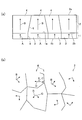
- (A) is a schematic diagram showing a cross section in which a group 13 element nitride crystal layer 2 is formed on an oriented polycrystalline sintered body 1, and (b) is a plan view of the group 13 element nitride crystal layer 2. It is the seen schematic diagram.
- (A) is a schematic diagram showing a cross section in which a group 13 element nitride crystal layer 2 is formed on an oriented polycrystalline sintered body 1, and (b) is a grain boundary 5 of the oriented polycrystalline sintered body 1. The state where the crack 7 has started to enter is shown, and (c) shows the state where the crack 8 has progressed along the grain boundary of the oriented polycrystalline sintered body 1.
- the oriented polycrystalline sintered body 1 is composed of a large number of single crystal particles 3, and there are grain boundaries 5 between adjacent single crystal particles 3.
- the crystal orientations of the single crystal particles 3 are not random but are aligned in a specific direction. This degree of orientation of crystal orientation is called the degree of orientation. That is, as shown in FIG. 1A, the crystal orientations A of the single crystal particles 3 are aligned to some extent.
- single crystal particle 3 extends between first main surface 1a and second main surface 1b of the oriented polycrystalline sintered body.
- the first main surface 1a is a crystal growth surface.
- the group 13 element nitride crystal layer 2 is epitaxially grown on the growth surface 1 a of the oriented polycrystalline sintered body 1. That is, the group 13 element nitride crystal layer 2 is grown so as to have a crystal orientation substantially following the crystal orientation of the oriented polycrystalline sintered body.
- Reference numeral 2 b denotes a growth start surface of the crystal layer 2
- reference numeral 2 a denotes a surface of the crystal layer 2.
- the crystal layer 2 is composed of a large number of single crystal particles 4, and there are grain boundaries 6 between adjacent single crystal particles 4.
- the crystal orientation B of the single crystal particles 4 is not random, but generally follows the orientation A of each single crystal particle 3 constituting the oriented polycrystalline sintered body as a base.
- the crystal orientations B of the single crystal grains 4 constituting the group 13 element nitride crystal layer 2 are aligned, but other crystal orientations of the single crystal grains 4 are as follows. It is not necessary to have them. That is, as shown in FIG. 1B, when each single crystal particle 4 is viewed planarly (from a direction parallel to the growth direction), the crystal orientations C and D are particularly random. There is no orientation. However, it is also possible to impart orientation to the crystal orientation of the single crystal particles 4 when viewed in plan.
- growth is performed by increasing the thickness T of the group 13 element nitride crystal layer 2 as compared with the thickness t of the oriented polycrystalline sintered body 1 serving as a base. It has been found that cracks are easily formed in the oriented polycrystalline sintered body due to the thermal stress during the subsequent temperature drop.
- the oriented polycrystalline sintered body 2 has a relatively uniform direction of the grain boundaries 5, so that when thermal stress is generated in the laminate, the stress is likely to concentrate on the grain boundaries. .
- the thickness of the oriented polycrystalline sintered body relatively, as shown in FIG. 2B, more thermal stress is applied to the grain boundaries 5 of the oriented polycrystalline sintered body 1. It becomes easy to concentrate and generation
- the thickness t (see FIG. 2A) of the oriented polycrystalline sintered body is 150 ⁇ m or more and 1 mm or less. By making this thickness 150 ⁇ m or more, handling during manufacture becomes easy. From this viewpoint, it is more preferable that the thickness t of the oriented polycrystalline sintered body is 190 ⁇ m or more. Further, by setting the thickness t of the oriented polycrystalline sintered body to 1 mm or less, the effect of relieving thermal stress by generating cracks along the grain boundaries of the oriented polycrystalline sintered body becomes more remarkable. From this viewpoint, the thickness t of the oriented polycrystalline sintered body is preferably 1 mm or less, and more preferably 500 ⁇ m or less.
- the material of the oriented polycrystalline sintered body is not particularly limited, but an oriented polycrystalline alumina sintered body, an oriented polycrystalline zinc oxide sintered body, or an oriented polycrystalline aluminum nitride sintered body is preferable.
- the oriented polycrystalline sintered body is composed of a sintered body including a large number of single crystal particles, and a large number of single crystal particles are oriented to some extent or highly in a certain direction.
- a hot isostatic pressing method HIP
- HP hot press method
- SPS spark plasma sintering
- the average particle size of the particles constituting the oriented polycrystalline sintered body on the surface of the sintered body is preferably 0.3 to 1000 ⁇ m, more preferably 3 to 1000 ⁇ m, still more preferably 10 ⁇ m to 200 ⁇ m, and particularly preferably 14 ⁇ m. ⁇ 200 ⁇ m.
- grains is measured with the following method. That is, the plate surface of the plate-like sintered body is polished and an image is taken with a scanning electron microscope.
- the visual field range is a visual field range in which a straight line intersecting 10 to 30 particles can be drawn when a straight line is drawn on the diagonal line of the obtained image.
- the orientation plane of the oriented polycrystalline sintered body is not particularly limited, and may be a c-plane, a-plane, r-plane, m-plane, or the like.
- the degree of orientation on the plate surface is preferably 50% or more, more preferably 65% or more, still more preferably 75% or more, particularly preferably 85%, and particularly preferably. 90% or more, and most preferably 95% or more.
- This degree of orientation is calculated by the following equation by measuring the XRD profile when X-rays are irradiated on the plate surface of plate-like alumina using an XRD apparatus (for example, RINT-TTR IV III manufactured by Rigaku Corporation). It is obtained by doing.
- oxides such as MgO, ZrO 2 , Y 2 O 3 , CaO, SiO 2 , TiO 2 , Fe 2 O 3 , Mn 2 O 3 , La 2 O 3 , Examples thereof include at least one selected from fluorides such as AlF 3 , MgF 2 and YbF 3 .
- the amount of the additive should be kept to the minimum necessary, and is preferably 5000 ppm or less, more preferably 1000 ppm or less, and still more preferably 700 ppm or less.
- the oriented polycrystalline sintered body is preferably smoothed by lapping using diamond abrasive grains after the plate surface is flattened by grinding with a grindstone.
- a group 13 element nitride crystal layer is grown on the oriented polycrystalline sintered body so as to have a crystal orientation that substantially follows the crystal orientation of the oriented polycrystalline sintered body.
- a seed crystal layer is first grown on the oriented polycrystalline sintered body.
- the method for producing the seed crystal layer is not particularly limited, but MOCVD (metal organic vapor phase epitaxy), MBE (molecular beam epitaxy), HVPE (hydride vapor phase epitaxy), sputtering and other gas phase methods, Na flux method, Preferred examples include liquid phase methods such as ammonothermal method, hydrothermal method, sol-gel method, powder method utilizing solid phase growth of powder, and combinations thereof.
- a low-temperature nitride layer is deposited at 20 to 50 nm at 450 to 550 ° C., and then a nitride layer having a thickness of 2 to 4 ⁇ m is laminated at 1000 to 1200 ° C. It is preferable to carry out.
- a group 13 element nitride crystal layer is formed on the seed crystal layer.
- This group 13 element nitride crystal layer is formed so as to have a crystal orientation substantially following the crystal orientation of the oriented polycrystalline sintered body.
- the method for forming the group 13 element nitride crystal layer is not particularly limited as long as it has a crystal orientation generally following the crystal orientation of the oriented polycrystalline sintered body, and is a gas phase method such as MOCVD or HVPE, a Na flux method, an ammono
- a liquid phase method such as a thermal method, a hydrothermal method, a sol-gel method, a powder method using solid phase growth of powder, and a combination thereof, but the Na flux method is particularly preferable.
- the formation of the group 13 element nitride crystal layer by the Na flux method is performed using a group 13 metal, metal Na, and a dopant (for example, germanium (Ge), silicon (Si), oxygen (O), etc.) in a crucible provided with a seed crystal substrate. Or a melt composition containing beryllium (Be), magnesium (Mg), calcium (Ca), strontium (Sr), zinc (Zn), cadmium (Cd) or the like. It is preferably carried out by heating and pressurizing to 830 to 910 ° C. and 3.5 to 4.5 MPa in a nitrogen atmosphere and then rotating while maintaining the temperature and pressure. The holding time varies depending on the target film thickness, but may be about 10 to 100 hours.
- a dopant for example, germanium (Ge), silicon (Si), oxygen (O), etc.
- the gallium nitride crystal thus obtained by the Na flux method is ground with a grindstone to flatten the plate surface, and then the plate surface is smoothed by lapping using diamond abrasive grains.
- the thickness T of the group 13 element nitride crystal layer is set to 5.5 to 20 times the thickness t of the oriented polycrystalline sintered body.
- T / t is preferably 5.5 or more, and more preferably 6 or more.
- T / t is more preferably 16 or less.
- a freestanding substrate including the group 13 element nitride crystal layer is obtained by separating the group 13 element nitride crystal layer from the oriented polycrystalline sintered body.
- the method for separating the group 13 element nitride crystal layer from the sintered body is not limited.
- the group 13 element nitride crystal layer is naturally separated from the oriented polycrystalline sintered body in the temperature lowering step after growing the group 13 element nitride crystal layer.
- the group 13 element nitride crystal layer can be separated from the oriented polycrystalline sintered body by chemical etching.
- the etchant is easily impregnated along the grain boundaries through the cracks. Therefore, separation of the group 13 element nitride crystal layer is facilitated. Can be promoted.
- strong acid such as sulfuric acid and hydrochloric acid, or strong alkali such as sodium hydroxide aqueous solution and potassium hydroxide aqueous solution is preferable.
- the temperature at which chemical etching is performed is preferably 70 ° C. or higher.
- the nitride constituting the group 13 element nitride crystal layer is one or more nitrides of group 13 elements defined by IUPAC.
- This group 13 element is preferably gallium, aluminum, or indium.
- the group 13 element nitride crystal specifically includes GaN, AlN, InN, Ga x Al 1-x N (1>x> 0), and Ga x In 1-x N (1>x> 0).
- Ga x Al y InN 1-xy (1>x> 0, 1>y> 0) is preferable.
- the group 13 element nitride crystal layer may not contain a dopant.
- the group 13 element nitride crystal layer may be doped with an n-type dopant or a p-type dopant.
- the p-type dopant include one or more selected from the group consisting of beryllium (Be), magnesium (Mg), calcium (Ca), strontium (Sr), zinc (Zn), and cadmium (Cd). It is done.
- Preferable examples of the n-type dopant include one or more selected from the group consisting of silicon (Si), germanium (Ge), tin (Sn), and oxygen (O).
- a free-standing substrate can be obtained by separating the group 13 element nitride crystal layer from the oriented polycrystalline sintered body.
- the “self-supporting substrate” means a substrate that can be handled as a solid material without being deformed or damaged by its own weight when handled.
- the gallium nitride free-standing substrate of the present invention can be used as a substrate for various semiconductor devices such as light-emitting elements, but in addition to this, an electrode (which may be a p-type electrode or an n-type electrode), a p-type layer, an n-type layer It can be used as a member or layer other than the substrate such as.
- the self-supporting substrate of the present invention comprises a plate composed of a plurality of group 13 element nitride single crystal particles having a single crystal structure in a substantially normal direction. That is, the self-supporting substrate is composed of a plurality of single crystal particles that are two-dimensionally connected in the horizontal plane direction, and therefore has a single crystal structure in the substantially normal direction. Therefore, the self-supporting substrate is not a single crystal as a whole, but has a single crystal structure in a local domain unit, and thus can have high crystallinity sufficient to ensure device characteristics such as a light emitting function. Nevertheless, the free standing substrate of the present invention is not a single crystal substrate.
- the plurality of single crystal particles constituting the self-supporting substrate have crystal orientations substantially aligned in a substantially normal direction.
- the crystal orientation that is generally aligned in the normal direction is not necessarily the crystal orientation that is perfectly aligned in the normal direction. As long as a device using a self-supporting substrate can secure desired device characteristics, It means that the crystal orientation may be aligned to some extent in similar directions.
- the group 13 element nitride single crystal particles have a structure grown substantially following the crystal orientation of the oriented polycrystalline sintered body.
- the “structure grown substantially following the crystal orientation of the oriented polycrystalline sintered body” means a structure brought about by crystal growth affected by the crystal orientation of the oriented polycrystalline sintered body, and is not necessarily oriented.
- the crystal of the oriented polycrystalline sintered body is not necessarily a structure that has grown completely following the crystal orientation of the crystalline sintered body, as long as a device such as a light-emitting element using a self-supporting substrate can ensure the desired device characteristics. It may be a structure grown to some extent along the direction. That is, this structure includes a structure that grows in a different crystal orientation from the oriented polycrystalline sintered body. In that sense, the expression “a structure grown substantially following the crystal orientation” can also be rephrased as “a structure grown substantially derived from the crystal orientation”.
- the free-standing substrate can have a structure in which the crystal orientations are substantially uniform with respect to the substantially normal direction.
- this self-supporting substrate is regarded as an aggregate of columnar-structured single crystal particles that are observed as single crystals when viewed in the normal direction and grain boundaries are observed when viewed in a cut surface in the horizontal plane direction. It is also possible.
- the “columnar structure” does not mean only a typical vertically long column shape, but includes various shapes such as a horizontally long shape, a trapezoidal shape, and a shape in which the trapezoid is inverted. Defined as meaning.
- the free-standing substrate may be a structure having a crystal orientation aligned to some extent in a normal line or a similar direction, and does not necessarily have a columnar structure in a strict sense.
- the cause of the columnar structure is considered to be that single crystal grains grow under the influence of the crystal orientation of the oriented polycrystalline sintered body used for manufacturing the gallium nitride free-standing substrate.
- the average grain size of the cross section of single crystal particles which can be said to be a columnar structure (hereinafter referred to as the average cross section diameter), depends not only on the film forming conditions but also on the average grain size of the plate surface of the oriented polycrystalline sintered body. it is conceivable that.
- the cross-sectional average diameter of the single crystal particles on the outermost surface of the self-supporting substrate is 0.3 ⁇ m or more, more preferably 3 ⁇ m or more, still more preferably 20 ⁇ m or more, particularly preferably 50 ⁇ m or more, and most preferably 70 ⁇ m or more.
- the upper limit of the cross-sectional average diameter of the single crystal particles on the outermost surface of the self-supporting substrate is not particularly limited, but 1000 ⁇ m or less is realistic, more practically 500 ⁇ m or smaller, and more practically 200 ⁇ m or smaller. .
- the self-supporting substrate preferably has a diameter of 50.8 mm (2 inches) or more, more preferably 100 mm (4 inches) or more, and even more preferably 200 mm (8 inches) or more.
- a light-emitting element is manufactured by providing a light-emitting functional layer on a free-standing substrate, and the formation of the light-emitting functional layer has a substantially normal direction so as to have a crystal orientation that substantially follows the crystal orientation of the free-standing substrate. It is preferable to form one or more layers composed of a plurality of semiconductor single crystal particles having a single crystal structure.
- a light-emitting element may be manufactured by using a self-supporting substrate as a member or layer other than a base material such as an electrode (which may be a p-type electrode or an n-type electrode), a p-type layer, or an n-type layer.
- a self-supporting substrate as a member or layer other than a base material such as an electrode (which may be a p-type electrode or an n-type electrode), a p-type layer, or an n-type layer.
- the self-supporting substrate of the present invention can be preferably used for various applications such as various electronic devices, power devices, light receiving elements, solar cell wafers as well as the above-described light emitting elements.
- Example A A laminated body was obtained according to the procedure described with reference to FIGS. 1 and 2, and the resulting gallium nitride crystal layer was naturally separated from the oriented polycrystalline sintered body to obtain a self-supporting substrate.
- the specific procedure is as follows.
- a plate-like alumina powder (manufactured by Kinsei Matec Co., Ltd., grade 00700) was prepared. 7 parts by weight of a binder (polyvinyl butyral: product number BM-2, manufactured by Sekisui Chemical Co., Ltd.) and a plasticizer (DOP: di (2-ethylhexyl) phthalate, Kurokin Kasei Co., Ltd.) per 100 parts by weight of the plate-like alumina particles 3.5 parts by weight), 2 parts by weight of a dispersant (Rheidol SP-O30, manufactured by Kao Corporation), and a dispersion medium (2-ethylhexanol) were mixed.
- a binder polyvinyl butyral: product number BM-2, manufactured by Sekisui Chemical Co., Ltd.
- DOP di (2-ethylhexyl) phthalate, Kurokin Kasei Co., Ltd.
- the amount of the dispersion medium was adjusted so that the slurry viscosity was 20000 cP.
- the slurry prepared as described above was formed into a sheet shape on a PET film by a doctor blade method so that the thickness after drying was 20 ⁇ m.
- the obtained tape was cut into a circular shape having a diameter of 50.8 mm (2 inches), 150 sheets were laminated, placed on an Al plate having a thickness of 10 mm, and then vacuum-packed. This vacuum pack was hydrostatically pressed in warm water at 85 ° C. at a pressure of 100 kgf / cm 2 to obtain a disk-shaped molded body.
- the obtained molded body was placed in a degreasing furnace and degreased at 600 ° C. for 10 hours.
- the obtained degreased body was fired in a nitrogen atmosphere at 1600 ° C. for 4 hours under a surface pressure of 200 kgf / cm 2 using a graphite mold.
- the obtained sintered body was fired again at 1700 ° C. for 2 hours in argon at a gas pressure of 1500 kgf / cm 2 by a hot one-pressure method (HIP).
- HIP hot one-pressure method
- the sintered body thus obtained was fixed to a ceramic surface plate and ground to # 2000 using a grindstone to flatten the plate surface.
- the surface of the plate was smoothed by lapping using diamond abrasive grains to obtain an oriented alumina sintered body 1 having a diameter of 50.8 mm (2 inches) and a thickness of 1 mm.
- the flatness was improved while gradually reducing the size of the abrasive grains from 3 ⁇ m to 0.5 ⁇ m.
- the average roughness Ra after processing was 1 nm.
- the average particle diameter of the plate surface was measured with the following method.
- the plate surface of the obtained oriented alumina substrate was polished and subjected to thermal etching at 1550 ° C. for 45 minutes, and then an image was taken with a scanning electron microscope.
- the visual field range was such that a straight line intersecting 10 to 30 particles could be drawn when a straight line was drawn on the diagonal line of the obtained image.
- the average particle size of the plate surface was 100 ⁇ m.
- a seed crystal layer was formed on the processed oriented alumina substrate using the MOCVD method. Specifically, after depositing a low-temperature GaN layer of 40 nm at 530 ° C., a GaN film having a thickness of 3 ⁇ m was laminated at 1050 ° C. to obtain a seed crystal substrate.
- the seed crystal substrate produced in the above process was placed on the bottom part of a cylindrical flat bottom alumina crucible having an inner diameter of 80 mm and a height of 45 mm, and then the melt composition was filled in the crucible in a glove box.
- the composition of the melt composition is as follows. ⁇ Metal Ga: 60g ⁇ Metal Na: 60g ⁇ Germanium tetrachloride: 1.85 g
- the alumina crucible was placed on a table that can rotate the crystal growth furnace. After heating and pressurizing up to 870 ° C. and 4.0 MPa in a nitrogen atmosphere, the solution was rotated for a certain period of time to grow a gallium nitride crystal while stirring. After the completion of crystal growth, the crystal was cooled to room temperature, and the gallium nitride crystal layer was naturally separated from the oriented alumina substrate. The melt composition remaining in the crucible was removed using ethanol, and the self-supporting substrate of gallium nitride crystal was recovered.
- the thickness of the gallium nitride crystal layer grown on the alumina substrate was changed as shown in Tables 1 and 2.
- the crystal growth time was adjusted in order to change the growth thickness of the gallium nitride crystal layer.
- Example B In the same manner as in Example 1 of Experiment A, a gallium nitride crystal layer was grown on an oriented alumina substrate. However, when the temperature was lowered, the gallium nitride crystal layer was not naturally peeled off by gradually cooling to room temperature over 12 hours.
- the resulting laminate was chemically etched to obtain a free-standing substrate made of a gallium nitride crystal layer. No cracks were found on the free-standing substrate.
- the conditions for chemical etching are as follows. It was immersed in 5% by mass sulfuric acid at 150 ° C. for 5 hours, or immersed in a 10% by mass aqueous sodium hydroxide solution at 70 ° C. for 5 hours.
Landscapes
- Chemical & Material Sciences (AREA)
- Engineering & Computer Science (AREA)
- Crystallography & Structural Chemistry (AREA)
- Materials Engineering (AREA)
- Metallurgy (AREA)
- Organic Chemistry (AREA)
- Inorganic Chemistry (AREA)
- Crystals, And After-Treatments Of Crystals (AREA)
Abstract
厚さが150μm以上、1mm以下の配向多結晶焼結体1上に、13族元素窒化物結晶層2を育成する。13族元素窒化物結晶層2の厚さTを配向多結晶焼結体1の厚さtの5.5倍以上、20倍以下とする。13族元素窒化物結晶層を配向多結晶焼結体から分離することによって13族元素窒化物結晶層を含む自立基板を得る。
Description
本発明は、13族元素窒化物結晶の自立基板およびこれを含む積層体に関するものである。
窒化ガリウム(GaN)単結晶上に各種GaN層を形成したLEDが注目されている。GaN単結晶基板であれば、GaN層と同種の材質であることから、格子定数及び熱膨張率が整合しやすく、サファイア基板を用いる場合よりも性能向上が期待できる。例えば、特許文献1(特開2010-132556号公報)には、厚みが200μm以上の自立したn型窒化ガリウム単結晶基板が開示されている。
しかしながら、単結晶基板は一般的に面積が小さく且つ高価なものである。特に、大面積基板を用いたLED製造の低コスト化が求められてきているが、大面積の単結晶基板を量産することは容易なことではなく、その製造コストはさらに高くなる。そこで、窒化ガリウム等の単結晶基板の代替材料となりうる安価な材料が望まれる。
そこで、本出願人は、低コストかつ大面積化が可能な配向多結晶アルミナ焼結体上に窒化ガリウム結晶を育成し、窒化ガリウム結晶の自立基板を作製することを提案した(特許文献2~4)。
しかし、配向多結晶アルミナ焼結体上に窒化ガリウム結晶層を育成する技術について、本発明者が更に検討を続けた結果、新たに以下の問題を見いだした。すなわち、配向多結晶アルミナ焼結体上に窒化ガリウム結晶層を育成して積層体を得た後、育成温度から室温へと降温する過程で、積層体が反ってしまい、窒化ガリウム結晶層にクラックが見られることがあった。
本発明の課題は、13族元素窒化物結晶層を配向多結晶焼結体上から分離して自立基板を得るのに際して、13族元素窒化物結晶層におけるクラックを抑制する方法を提供することである。
本発明は、厚さが150μm以上、1mm以下の配向多結晶焼結体上に、13族元素窒化物結晶層を育成し、13族元素窒化物結晶層の厚さが配向多結晶焼結体の厚さの5.5倍以上、20倍以下である工程、および
13族元素窒化物結晶層を配向多結晶焼結体から分離することによって13族元素窒化物結晶層を含む自立基板を得る工程
を有することを特徴とする、自立基板の製造方法に係るものである。
13族元素窒化物結晶層を配向多結晶焼結体から分離することによって13族元素窒化物結晶層を含む自立基板を得る工程
を有することを特徴とする、自立基板の製造方法に係るものである。
また、本発明は、厚さが150μm以上、1mm以下の配向多結晶焼結体、および
配向多結晶焼結体上に設けられた13族元素窒化物結晶層であって、13族元素窒化物結晶層の厚さが配向多結晶焼結体の厚さの5.5倍以上、20倍以下である13族元素窒化物結晶層を有することを特徴とする、積層体に係るものである。
配向多結晶焼結体上に設けられた13族元素窒化物結晶層であって、13族元素窒化物結晶層の厚さが配向多結晶焼結体の厚さの5.5倍以上、20倍以下である13族元素窒化物結晶層を有することを特徴とする、積層体に係るものである。
本発明者は、配向多結晶焼結体上に13族元素窒化物結晶層を育成するのに際して、下地となる配向多結晶焼結体の厚さに比べて、13族元素窒化物結晶層の厚さを大きくすることによって、育成後の降温時の熱応力によって配向多結晶焼結体にクラックが入りやすくなることを見いだした。この結果として、積層体の反りが緩和され、13族元素窒化物結晶層中でクラックが発生しにくくなる。
こうした配向多結晶焼結体に生じたクラックを更に観察することによって、以下の知見を得た。すなわち、配向多結晶焼結体の粒界に沿って微細なクラックが多数発生しており、熱応力が緩和されやすかったものと考えられる。配向多結晶焼結体は、粒界の方向が比較的揃っているので、積層体に熱応力が発生したときに粒界に応力が集中し易い。これに加えて、配向多結晶焼結体の厚さを相対的に小さくすることで、配向多結晶焼結体の粒界に、より熱応力が集中し易いようにし、微細なクラックの発生を促進することで、積層体の反りと13族元素窒化物結晶層中のクラックを抑制できたものと考えられる。
以下、適宜図面を参照しつつ、本発明を更に説明する。
図1(a)に模式的に示すように、配向多結晶焼結体1は、多数の単結晶粒子3からなっており、隣接する単結晶粒子3間には粒界5がある。配向多結晶焼結体においては、単結晶粒子3の結晶方位がランダムではなく、特定方向に向かって揃っている。この結晶方位の配向の度合いを配向度と呼んでいる。すなわち、図1(a)に示すように、各単結晶粒子3の結晶方位Aはある程度揃っている。また、好ましくは、単結晶粒子3は、配向多結晶焼結体の第一の主面1aと第二の主面1bとの間に延びている。本例では第一の主面1aを結晶育成面としている。
図1(a)に模式的に示すように、配向多結晶焼結体1は、多数の単結晶粒子3からなっており、隣接する単結晶粒子3間には粒界5がある。配向多結晶焼結体においては、単結晶粒子3の結晶方位がランダムではなく、特定方向に向かって揃っている。この結晶方位の配向の度合いを配向度と呼んでいる。すなわち、図1(a)に示すように、各単結晶粒子3の結晶方位Aはある程度揃っている。また、好ましくは、単結晶粒子3は、配向多結晶焼結体の第一の主面1aと第二の主面1bとの間に延びている。本例では第一の主面1aを結晶育成面としている。
次いで、配向多結晶焼結体1の育成面1a上に13族元素窒化物結晶層2をエピタキシャル成長させる。すなわち、配向多結晶焼結体の結晶方位に概ね倣った結晶方位を有するように、13族元素窒化物結晶層2が育成される。2bは、結晶層2の成長開始面であり、2aは結晶層2の表面である。結晶層2は、多数の単結晶粒子4からなっており、隣接する単結晶粒子4間には粒界6がある。結晶層3においては、単結晶粒子4の結晶方位Bがランダムではなく、下地となる配向多結晶焼結体を構成する各単結晶粒子3の方位Aに概ね倣っている。
ただし、図1(a)に示す横断面では、13族元素窒化物結晶層2を構成する各単結晶粒子4の結晶方位Bは揃っているが、単結晶粒子4の他の結晶方位については揃っている必要はない。すなわち、図1(b)に示すように、各単結晶粒子4を平面的に(育成方向に向かって平行な方向から)見た場合には、結晶方位C、Dはランダムになっており特に配向性はない。ただし、平面的に見た場合に単結晶粒子4の結晶方位に配向性を付与することも可能である。
ここで、図2(a)に示すように、下地となる配向多結晶焼結体1の厚さtに比べて、13族元素窒化物結晶層2の厚さTを大きくすることによって、育成後の降温時の熱応力によって配向多結晶焼結体にクラックが入りやすくなることを見いだした。
すなわち、降温後の積層体を観察してみると、図2(c)に示すように、配向多結晶焼結体1の粒界5に沿って微細なクラック8が多数発生していた。こうしたクラックによって、積層体に加わる熱応力が緩和され、反りが抑制され、この結果として13族元素窒化物結晶層2におけるクラックが抑制されたものと考えられる。
この機構であるが、配向多結晶焼結体2は、粒界5の方向が比較的揃っているので、積層体に熱応力が発生したときに粒界に応力が集中し易いものと考えられる。これに加えて、配向多結晶焼結体の厚さを相対的に小さくすることで、図2(b)に示すように、配向多結晶焼結体1の粒界5に、より熱応力が集中し易いようになり、微細なクラック7の発生が促進される。このクラック7が図2(c)に示すように進展することで、積層体の反りと13族元素窒化物結晶層中のクラックを抑制できたものと考えられる。
以下、本発明の各構成要素について更に述べる。
(配向多結晶焼結体)
配向多結晶焼結体の厚さt(図2(a)参照)は、150μm以上、1mm以下とする。この厚さを150μm以上とすることによって、製造時の取り扱いが容易になる。また、この観点からは、配向多結晶焼結体の厚さtを190μm以上とすることが更に好ましい。また、配向多結晶焼結体の厚さtを1mm以下とすることによって、配向多結晶焼結体の粒界に沿ってクラックを生じさせて熱応力を緩和する作用効果が一層顕著になる。この観点からは、配向多結晶焼結体の厚さtは、1mm以下が好ましく、500μm以下が更に好ましい。
(配向多結晶焼結体)
配向多結晶焼結体の厚さt(図2(a)参照)は、150μm以上、1mm以下とする。この厚さを150μm以上とすることによって、製造時の取り扱いが容易になる。また、この観点からは、配向多結晶焼結体の厚さtを190μm以上とすることが更に好ましい。また、配向多結晶焼結体の厚さtを1mm以下とすることによって、配向多結晶焼結体の粒界に沿ってクラックを生じさせて熱応力を緩和する作用効果が一層顕著になる。この観点からは、配向多結晶焼結体の厚さtは、1mm以下が好ましく、500μm以下が更に好ましい。
配向多結晶焼結体の材質は、特に限定されないが、配向多結晶アルミナ焼結体、配向多結晶酸化亜鉛焼結体、または配向多結晶窒化アルミニウム焼結体が好ましい。
配向多結晶焼結体は、多数の単結晶粒子を含んで構成される焼結体からなり、多数の単結晶粒子が一定の方向にある程度又は高度に配向したものである。このように配向された多結晶焼結体を用いることで、略法線方向に概ね揃った結晶方位を有する自立基板を作製可能である。
配向多結晶焼結体を得る製法としては、大気炉、窒素雰囲気炉、水素雰囲気炉等を用いた通常の常圧焼結法に加え、熱間等方圧加圧法(HIP)、ホットプレス法(HP)、放電プラズマ焼結(SPS)等の加圧焼結法、及びこれらを組み合わせた方法を用いることができる。
配向多結晶焼結体を構成する粒子の焼結体表面における平均粒径は、0.3~1000μmであるのが好ましく、より好ましくは3~1000μm、さらに好ましくは10μm~200μm、特に好ましくは14μm~200μmである。
なお、焼結体粒子の板面における平均粒径は以下の方法により測定されるものである。すなわち、板状焼結体の板面を研磨し、走査電子顕微鏡にて画像を撮影する。視野範囲は、得られる画像の対角線に直線を引いた場合に、いずれの直線も10個から30個の粒子と交わるような直線が引けるような視野範囲とする。得られた画像の対角線に2本の直線を引いて、直線が交わる全ての粒子に対し、個々の粒子の内側の線分の長さを平均したものに1.5を乗じた値を板面の平均粒径とする。なお、板面の走査顕微鏡像で明瞭に焼結体粒子の界面を判別できない場合は、サーマルエッチング(例えば1550℃で45分間)やケミカルエッチングによって界面を際立たせる処理を施した後に上記の評価を行ってもよい。
また、配向多結晶焼結体の配向面は特に限定がなく、c面、a面、r面又はm面等であってもよい。
また、配向多結晶焼結体の配向面は特に限定がなく、c面、a面、r面又はm面等であってもよい。
配向度については、例えば、板面における配向度が50%以上であるのが好ましく、より好ましくは65%以上、さらに好ましくは75%以上であり、特に好ましくは85%であり、特により好ましくは90%以上であり、最も好ましくは95%以上である。この配向度は、XRD装置(例えば、株式会社リガク製、RINT-TTR III)を用い、板状アルミナの板面に対してX線を照射したときのXRDプロファイルを測定し、以下の式により算出することにより得られるものである。

配向多結晶焼結体の焼結助剤として、MgO、ZrO2、Y2O3、CaO、SiO2、TiO2、Fe2O3、Mn2O3、La2O3等の酸化物、AlF3、MgF2、YbF3等のフッ化物などから選ばれる少なくとも1種以上が挙げられる。透光性の観点では添加物の量は必要最小限に留めるべきであり、好ましくは5000ppm以下、より好ましくは1000ppm以下、さらに好ましくは700ppm以下である。
配向多結晶焼結体は、砥石で研削して板面を平坦にした後、ダイヤモンド砥粒を用いたラップ加工により板面を平滑化するのが好ましい。
配向多結晶焼結体は、砥石で研削して板面を平坦にした後、ダイヤモンド砥粒を用いたラップ加工により板面を平滑化するのが好ましい。
次いで、配向多結晶焼結体上に、13族元素窒化物結晶層を、配向多結晶焼結体の結晶方位に概ね倣った結晶方位を有するように育成する。
この際には、好ましくは、まず配向多結晶焼結体上に種結晶層を育成する。種結晶層の作製方法は特に限定されないが、MOCVD(有機金属気相成長法)、MBE(分子線エピタキシー法)、HVPE(ハイドライド気相成長法)、スパッタリング等の気相法、Naフラックス法、アモノサーマル法、水熱法、ゾルゲル法等の液相法、粉末の固相成長を利用した粉末法、及びこれらの組み合わせが好ましく例示される。例えば、MOCVD法による種結晶層の形成は、450~550℃にて低温窒化物層を20~50nm堆積させた後に、1000~1200℃にて厚さ2~4μmの窒化物層を積層させることにより行うのが好ましい。
次いで、種結晶層上に13族元素窒化物結晶層を形成する。この13族元素窒化物結晶層は、配向多結晶焼結体の結晶方位に概ね倣った結晶方位を有するように形成する。13族元素窒化物結晶層の形成方法は、配向多結晶焼結体の結晶方位に概ね倣った結晶方位を有する限り特に限定がなく、MOCVD、HVPE等の気相法、Naフラックス法、アモノサーマル法、水熱法、ゾルゲル法等の液相法、粉末の固相成長を利用した粉末法、及びこれらの組み合わせが好ましく例示されるが、Naフラックス法により行われるのが特に好ましい。
Naフラックス法による13族元素窒化物結晶層の形成は、種結晶基板を設置した坩堝に13族金属、金属Na及び所望によりドーパント(例えばゲルマニウム(Ge)、シリコン(Si)、酸素(O)等のn型ドーパント、又はベリリウム(Be)、マグネシウム(Mg)、カルシウム(Ca)、ストロンチウム(Sr)、亜鉛(Zn)、カドミウム(Cd)等のp型ドーパント)を含む融液組成物を充填し、窒素雰囲気中で830~910℃、3.5~4.5MPaまで昇温加圧した後、温度及び圧力を保持しつつ回転することにより行うのが好ましい。保持時間は目的の膜厚によって異なるが、10~100時間程度としてもよい。
また、こうしてNaフラックス法により得られた窒化ガリウム結晶を砥石で研削して板面を平坦にした後、ダイヤモンド砥粒を用いたラップ加工により板面を平滑化するのが好ましい。
ここで、13族元素窒化物結晶層の厚さTを、配向多結晶焼結体の厚さtの5.5倍以上、20倍以下とする。この比率T/tを5.5以上とすることによって、13族元素窒化物結晶層の育成後の降温時に配向多結晶焼結体の粒界に沿って微細なクラックが入りやすくなり、積層体の反りや13族元素窒化物結晶層のクラックを抑制できる。この観点からは、T/tは、5.5以上とすることが好ましく、6以上とすることが更に好ましい。
また、この比率T/tを20以下とすることによって、13族元素窒化物結晶層の成膜に要する時間とコストを低減できる。この観点からは、T/tを16以下とすることが更に好ましい。
次いで、13族元素窒化物結晶層を前記配向多結晶焼結体から分離することによって13族元素窒化物結晶層を含む自立基板を得る。
ここで、13族元素窒化物結晶層を焼結体から分離する方法は限定されない。好適な実施形態においては、13族元素窒化物結晶層を育成した後の降温工程において13族元素窒化物結晶層を配向多結晶焼結体から自然剥離させる。
ここで、13族元素窒化物結晶層を焼結体から分離する方法は限定されない。好適な実施形態においては、13族元素窒化物結晶層を育成した後の降温工程において13族元素窒化物結晶層を配向多結晶焼結体から自然剥離させる。
あるいは、13族元素窒化物結晶層を前記配向多結晶焼結体からケミカルエッチングによって分離することができる。本発明では、配向多結晶焼結体の粒界に沿って微細なクラックが多数入っているので、そのクラックを通して粒界に沿ってエッチャントが含浸されやすく、ゆえに13族元素窒化物結晶層の分離を促進できる。
ケミカルエッチングを行う際のエッチャントとしては、硫酸、塩酸等の強酸、もしくは水酸化ナトリウム水溶液、水酸化カリウム水溶液等の強アルカリが好ましい。また、ケミカルエッチングを行う際の温度は、70℃以上が好ましい。
13族元素窒化物結晶層を構成する窒化物は、IUPACで規定する13族元素の一種または二種以上の窒化物である。この13族元素は、好ましくはガリウム、アルミニウム、インジウムである。また、13族元素窒化物結晶は、具体的には、GaN、AlN、InN、GaxAl1-xN(1>x>0)、GaxIn1-xN(1>x>0)、GaxAlyInN1―x-y(1>x>0、1>y>0)が好ましい。
13族元素窒化物結晶層は、ドーパントを含まないものであってもよい。あるいは、13族元素窒化物結晶層は、n型ドーパント又はp型ドーパントでドープされていてもよい。p型ドーパントの好ましい例としては、ベリリウム(Be)、マグネシウム(Mg)、カルシウム(Ca)、ストロンチウム(Sr)、亜鉛(Zn)及びカドミウム(Cd)からなる群から選択される1種以上が挙げられる。n型ドーパントの好ましい例としては、シリコン(Si)、ゲルマニウム(Ge)、スズ(Sn)及び酸素(O)からなる群から選択される1種以上が挙げられる。
13族元素窒化物結晶層を配向多結晶焼結体から分離することで、自立基板を得ることができる。本発明において「自立基板」とは、取り扱う際に自重で変形又は破損せず、固形物として取り扱うことのできる基板を意味する。本発明の窒化ガリウム自立基板は発光素子等の各種半導体デバイスの基板として使用可能であるが、それ以外にも、電極(p型電極又はn型電極でありうる)、p型層、n型層等の基材以外の部材又は層として使用可能なものである。
本発明の自立基板は、略法線方向に単結晶構造を有する複数の13族元素窒化物単結晶粒子で構成される板からなる。すなわち、自立基板は、水平面方向に二次元的に連結されてなる複数の単結晶粒子で構成されており、それ故、略法線方向には単結晶構造を有することになる。したがって、自立基板は、全体としては単結晶ではないものの、局所的なドメイン単位では単結晶構造を有するため、発光機能等のデバイス特性を確保するのに十分な高い結晶性を有することができる。そうでありながら、本発明の自立基板は単結晶基板ではない。
好ましくは、自立基板を構成する複数の単結晶粒子は、略法線方向に概ね揃った結晶方位を有する。「略法線方向に概ね揃った結晶方位」とは、必ずしも法線方向に完全に揃った結晶方位とは限らず、自立基板を用いたデバイスが所望のデバイス特性を確保できるかぎり、法線ないしそれに類する方向にある程度揃った結晶方位であってよいことを意味する。製法由来の表現をすれば、13族元素窒化物単結晶粒子は、配向多結晶焼結体の結晶方位に概ね倣って成長した構造を有する。「配向多結晶焼結体の結晶方位に概ね倣って成長した構造」とは、配向多結晶焼結体の結晶方位の影響を受けた結晶成長によりもたらされた構造を意味し、必ずしも配向多結晶焼結体の結晶方位に完全に倣って成長した構造であるとは限らず、自立基板を用いた発光素子等のデバイスが所望のデバイス特性を確保できるかぎり、配向多結晶焼結体の結晶方位にある程度倣って成長した構造であってよい。すなわち、この構造は配向多結晶焼結体と異なる結晶方位に成長する構造も含む。その意味で、「結晶方位に概ね倣って成長した構造」との表現は「結晶方位に概ね由来して成長した構造」と言い換えることもでき、この言い換え及び上記意味は本明細書中の同種の表現に同様に当てはまる。したがって、そのような結晶成長はエピタキシャル成長によるものが好ましいが、これに限定されず、それに類する様々な結晶成長の形態であってもよい。いずれにしても、このように成長することで、自立基板は略法線方向に関しては結晶方位が概ね揃った構造とすることができる。
したがって、本自立基板は、法線方向に見た場合に単結晶と観察され、水平面方向の切断面で見た場合に粒界が観察される柱状構造の単結晶粒子の集合体であると捉えることも可能である。ここで、「柱状構造」とは、典型的な縦長の柱形状のみを意味するのではなく、横長の形状、台形の形状、及び台形を逆さにしたような形状等、種々の形状を包含する意味として定義される。もっとも、上述のとおり、自立基板は法線ないしそれに類する方向にある程度揃った結晶方位を有する構造であればよく、必ずしも厳密な意味で柱状構造である必要はない。柱状構造となる原因は、前述のとおり、窒化ガリウム自立基板の製造に用いられる配向多結晶焼結体の結晶方位の影響を受けて単結晶粒子が成長するためと考えられる。このため、柱状構造ともいえる単結晶粒子の断面の平均粒径(以下、断面平均径という)は成膜条件だけでなく、配向多結晶焼結体の板面の平均粒径にも依存するものと考えられる。
好ましくは、自立基板の最表面における単結晶粒子の断面平均径は0.3μm以上であり、より好ましくは3μm以上、さらに好ましくは20μm以上、特に好ましくは50μm以上、最も好ましくは70μm以上である。また、自立基板の最表面における単結晶粒子の断面平均径の上限は特に限定されないが、1000μm以下が現実的であり、より現実的には500μm以下であり、さらに現実的には200μm以下である。
自立基板は直径50.8mm(2インチ)以上の大きさを有するのが好ましく、より好ましくは直径100mm(4インチ)以上であり、さらに好ましくは直径200mm(8インチ)以上である。
本発明の自立基板を用いた発光素子の構造やその作製方法は特に限定されるものではない。典型的には、発光素子は、自立基板に発光機能層を設けることにより作製され、この発光機能層の形成は、自立基板の結晶方位に概ね倣った結晶方位を有するように、略法線方向に単結晶構造を有する複数の半導体単結晶粒子で構成される層を一つ以上形成することに行われるのが好ましい。もっとも、自立基板を電極(p型電極又はn型電極でありうる)、p型層、n型層等の基材以外の部材又は層として利用して発光素子を作製してもよい。
本発明の自立基板は、上述した発光素子のみならず、各種電子デバイス、パワーデバイス、受光素子、太陽電池用ウェハー等の種々の用途に好ましく利用することができる。
(実験A)
図1、図2を参照しつつ説明した手順に従い、積層体を得、得られた窒化ガリウム結晶層を配向多結晶焼結体から自然剥離させて自立基板を得た。ただし、具体的手順は以下のとおりである。
図1、図2を参照しつつ説明した手順に従い、積層体を得、得られた窒化ガリウム結晶層を配向多結晶焼結体から自然剥離させて自立基板を得た。ただし、具体的手順は以下のとおりである。
(c面配向アルミナ焼結体の作製)
原料として、板状アルミナ粉末(キンセイマテック株式会社製、グレード00610)を用意した。板状アルミナ粒子100重量部に対し、バインダー(ポリビニルブチラール:品番BM-2、積水化学工業株式会社製)7重量部と、可塑剤(DOP:ジ(2-エチルヘキシル)フタレート、黒金化成株式会社製)3.5重量部と、分散剤(レオドールSP-O30、花王株式会社製)2重量部と、分散媒(2-エチルヘキサノール)を混合した。分散媒の量は、スラリー粘度が20000cPとなるように調整した。上記のようにして調製されたスラリーを、ドクターブレード法によって、PETフィルムの上に、乾燥後の厚さが20μmとなるように、シート状に成形した。得られたテープを口径50.8mm(2インチ)の円形に切断した後150枚積層し、厚さ10mmのAl板の上に載置した後、真空パックを行った。この真空パックを85℃の温水中で、100kgf/cm2の圧力にて静水圧プレスを行い、円盤状の成形体を得た。
原料として、板状アルミナ粉末(キンセイマテック株式会社製、グレード00610)を用意した。板状アルミナ粒子100重量部に対し、バインダー(ポリビニルブチラール:品番BM-2、積水化学工業株式会社製)7重量部と、可塑剤(DOP:ジ(2-エチルヘキシル)フタレート、黒金化成株式会社製)3.5重量部と、分散剤(レオドールSP-O30、花王株式会社製)2重量部と、分散媒(2-エチルヘキサノール)を混合した。分散媒の量は、スラリー粘度が20000cPとなるように調整した。上記のようにして調製されたスラリーを、ドクターブレード法によって、PETフィルムの上に、乾燥後の厚さが20μmとなるように、シート状に成形した。得られたテープを口径50.8mm(2インチ)の円形に切断した後150枚積層し、厚さ10mmのAl板の上に載置した後、真空パックを行った。この真空パックを85℃の温水中で、100kgf/cm2の圧力にて静水圧プレスを行い、円盤状の成形体を得た。
得られた成形体を脱脂炉中に配置し、600℃で10時間の条件で脱脂を行った。得られた脱脂体を黒鉛製の型を用い、ホットプレスにて窒素中1600℃で4時間、面圧200kgf/cm2の条件で焼成した。得られた焼結体を熱間当方圧加圧法(HIP)にてアルゴン中1700℃で2時間、ガス圧1500kgf/cm2の条件で再度焼成した。
このようにして得た焼結体をセラミックスの定盤に固定し、砥石を用いて#2000まで研削して板面を平坦にした。次いで、ダイヤモンド砥粒を用いたラップ加工により、板面を平滑化し、口径50.8mm(2インチ)、厚さ1mmの配向アルミナ焼結体1を得た。砥粒のサイズを3μmから0.5μmまで段階的に小さくしつつ、平坦性を高めた。加工後の平均粗さRaは1nmであった。
(配向アルミナ基板の評価)
得られた配向アルミナ基板の配向度を確認するため、XRDにより本実験例における測定対象とする結晶面であるc面の配向度を測定した。XRD装置(株式会社リガク製、RINT-TTR III)を用い、配向アルミナ基板の板面に対してX線を照射したときの2θ=20~70°の範囲でXRDプロファイルを測定した。c面配向度は、以下の式により算出した。この結果、本実験例におけるc面配向度の値は97%であった。
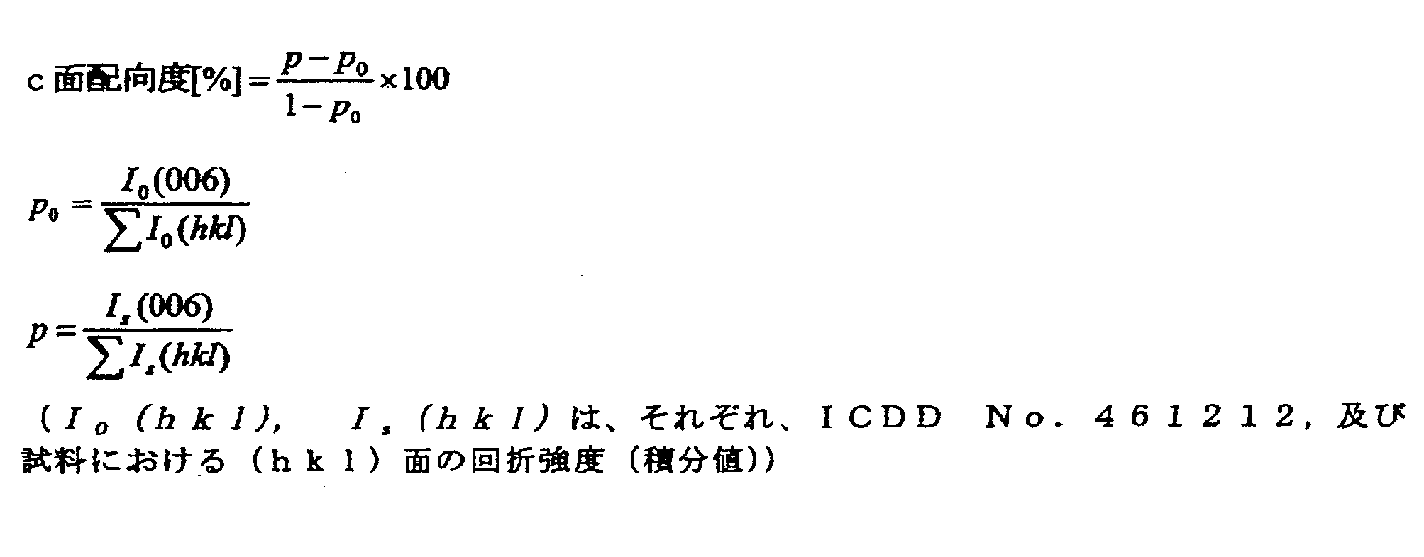
得られた配向アルミナ基板の配向度を確認するため、XRDにより本実験例における測定対象とする結晶面であるc面の配向度を測定した。XRD装置(株式会社リガク製、RINT-TTR III)を用い、配向アルミナ基板の板面に対してX線を照射したときの2θ=20~70°の範囲でXRDプロファイルを測定した。c面配向度は、以下の式により算出した。この結果、本実験例におけるc面配向度の値は97%であった。
(焼結体粒子の粒径評価)
配向アルミナ基板の焼結体粒子について、板面の平均粒径を以下の方法により測定した。得られた配向アルミナ基板の板面を研磨し、1550℃で45分間サーマルエッチングを行った後、走査電子顕微鏡にて画像を撮影した。視野範囲は、得られる画像の対角線に直線を引いた場合に、いずれの直線も10個から30個の粒子と交わるような直線が引けるような視野範囲とした。得られた画像の対角線に引いた2本の直線において、直線が交わる全ての粒子に対し、個々の粒子の内側の線分の長さを平均したものに1.5を乗じた値を板面の平均粒径とした。この結果、板面の平均粒径は100μmであった。
配向アルミナ基板の焼結体粒子について、板面の平均粒径を以下の方法により測定した。得られた配向アルミナ基板の板面を研磨し、1550℃で45分間サーマルエッチングを行った後、走査電子顕微鏡にて画像を撮影した。視野範囲は、得られる画像の対角線に直線を引いた場合に、いずれの直線も10個から30個の粒子と交わるような直線が引けるような視野範囲とした。得られた画像の対角線に引いた2本の直線において、直線が交わる全ての粒子に対し、個々の粒子の内側の線分の長さを平均したものに1.5を乗じた値を板面の平均粒径とした。この結果、板面の平均粒径は100μmであった。
(種結晶層の成膜)
次に、加工した配向アルミナ基板の上に、MOCVD法を用いて種結晶層を形成した。具体的には、530℃にて低温GaN層を40nm堆積させた後に、1050℃にて厚さ3μmのGaN膜を積層させて種結晶基板を得た。
次に、加工した配向アルミナ基板の上に、MOCVD法を用いて種結晶層を形成した。具体的には、530℃にて低温GaN層を40nm堆積させた後に、1050℃にて厚さ3μmのGaN膜を積層させて種結晶基板を得た。
(Naフラックス法によるGeドープGaN層の成膜)
上記工程で作製した種結晶基板を、内径80mm、高さ45mmの円筒平底のアルミナ坩堝の底部分に設置し、次いで融液組成物をグローブボックス内で坩堝内に充填した。融液組成物の組成は以下のとおりである。
・金属Ga:60g
・金属Na:60g
・四塩化ゲルマニウム:1.85g
上記工程で作製した種結晶基板を、内径80mm、高さ45mmの円筒平底のアルミナ坩堝の底部分に設置し、次いで融液組成物をグローブボックス内で坩堝内に充填した。融液組成物の組成は以下のとおりである。
・金属Ga:60g
・金属Na:60g
・四塩化ゲルマニウム:1.85g
このアルミナ坩堝を耐熱金属製の容器に入れて密閉した後、結晶育成炉の回転が可能な台上に設置した。窒素雰囲気中で870℃、4.0MPaまで昇温加圧後、一定時間溶液を回転することで、撹拌しながら窒化ガリウム結晶を成長させた。結晶成長終了後、室温まで冷却し、窒化ガリウム結晶層を配向アルミナ基板から自然剥離させた。エタノールを用いて、坩堝内に残った融液組成物を除去し、窒化ガリウム結晶の自立基板を回収した。
ただし、アルミナ基板上に育成する窒化ガリウム結晶層の厚さは、表1、表2に示すように変更した。また、窒化ガリウム結晶層の育成厚さを変更するため、結晶成長時間を調整した。

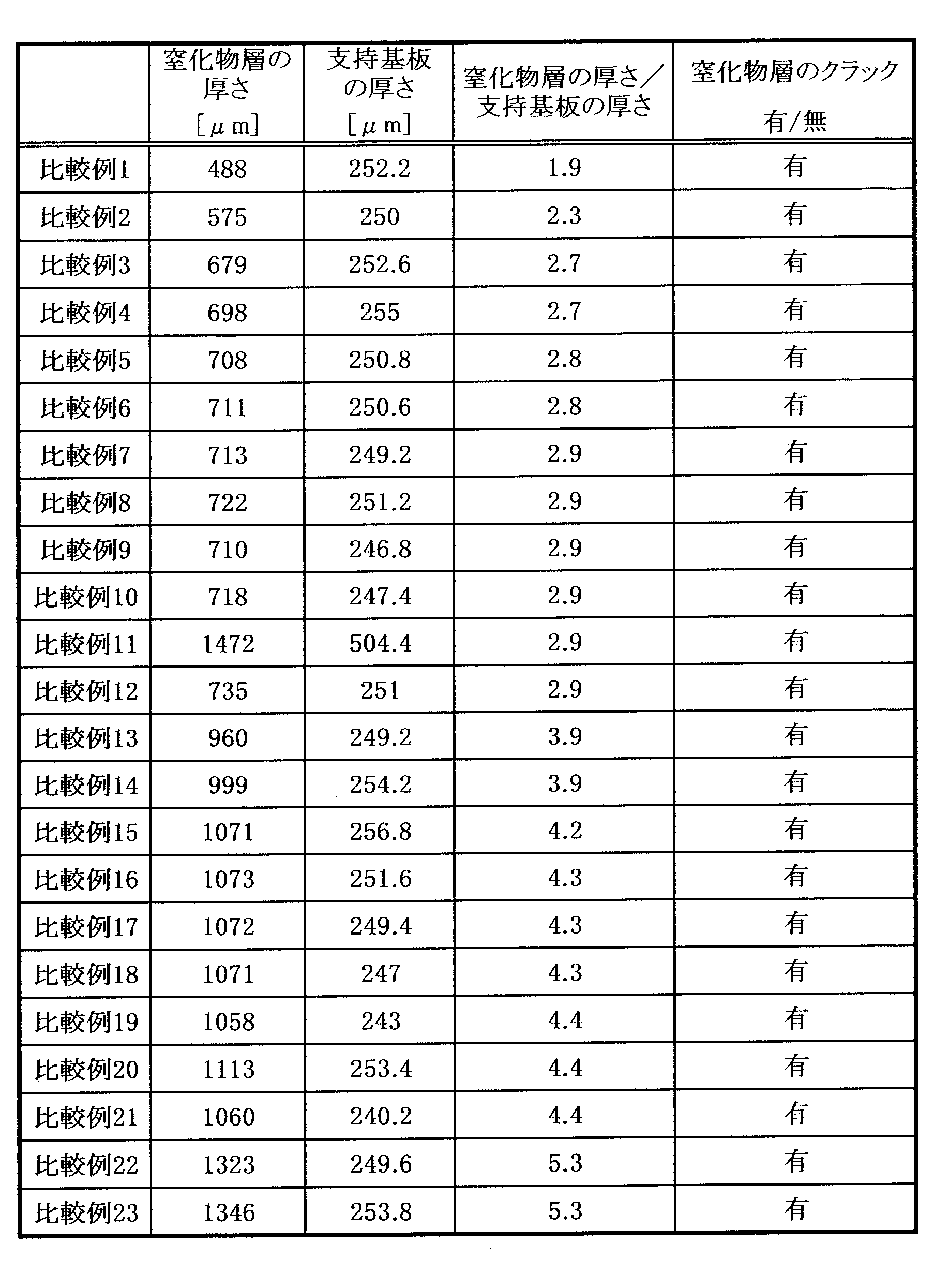
表1に示すように、本発明実施例1~13では、得られた自立基板にクラックがみられなかった。一方、表2に示すように比較例1~23では、自立基板にクラックがみられた。
(実験B)
実験Aの実施例1と同様にして、配向アルミナ基板上に窒化ガリウム結晶層を育成した。ただし、降温時に、室温への降温に12時間かけて徐冷することによって、窒化ガリウム結晶層の自然剥離を生じさせないようにした。
実験Aの実施例1と同様にして、配向アルミナ基板上に窒化ガリウム結晶層を育成した。ただし、降温時に、室温への降温に12時間かけて徐冷することによって、窒化ガリウム結晶層の自然剥離を生じさせないようにした。
得られた積層体をケミカルエッチングすることによって、窒化ガリウム結晶層からなる自立基板を得た。自立基板にはクラックはみられなかった。なお、ケミカルエッチングの条件は以下のとおりである。5質量%硫酸中に150℃5時間浸漬、または10質量%水酸化ナトリウム水溶液中に70℃5時間浸漬した。
Claims (7)
- 厚さが150μm以上、1mm以下の配向多結晶焼結体上に、13族元素窒化物結晶層を育成し、前記13族元素窒化物結晶層の厚さが前記配向多結晶焼結体の厚さの5.5倍以上、20倍以下である工程、および
前記13族元素窒化物結晶層を前記配向多結晶焼結体から分離することによって前記13族元素窒化物結晶層を含む自立基板を得る工程
を有することを特徴とする、自立基板の製造方法。 - 前記13族元素窒化物結晶層を育成した後の降温工程において前記13族元素窒化物結晶層を前記配向多結晶焼結体から自然剥離させることを特徴とする、請求項1記載の方法。
- 前記13族元素窒化物結晶層を前記配向多結晶焼結体からケミカルエッチングによって分離することを特徴とする、請求項1記載の方法。
- 前記13族元素窒化物結晶層をナトリウムフラックス法によって育成することを特徴とする、請求項1~3のいずれか一つの請求項に記載の方法。
- 前記配向多結晶焼結体が配向多結晶アルミナ焼結体であり、前記前記13族元素窒化物結晶層が、窒化ガリウム、窒化アルミニウム、窒化インジウムまたはこれらの混晶からなることを特徴とする、請求項1~4のいずれか一つの請求項に記載の方法。
- 厚さが150μm以上、1mm以下の配向多結晶焼結体、および
前記配向多結晶焼結体上に設けられた13族元素窒化物結晶層であって、前記13族元素窒化物結晶層の厚さが前記配向多結晶焼結体の厚さの5.5倍以上、20倍以下である13族元素窒化物結晶層
を有することを特徴とする、積層体 - 前記配向多結晶焼結体が配向多結晶アルミナ焼結体であり、前記前記13族元素窒化物結晶層が、窒化ガリウム、窒化アルミニウム、窒化インジウムまたはこれらの混晶からなることを特徴とする、請求項6記載の積層体。
Priority Applications (1)
| Application Number | Priority Date | Filing Date | Title |
|---|---|---|---|
| JP2018508911A JP6812413B2 (ja) | 2016-03-29 | 2017-03-09 | 自立基板および積層体 |
Applications Claiming Priority (2)
| Application Number | Priority Date | Filing Date | Title |
|---|---|---|---|
| JP2016-065343 | 2016-03-29 | ||
| JP2016065343 | 2016-03-29 |
Publications (1)
| Publication Number | Publication Date |
|---|---|
| WO2017169622A1 true WO2017169622A1 (ja) | 2017-10-05 |
Family
ID=59963125
Family Applications (1)
| Application Number | Title | Priority Date | Filing Date |
|---|---|---|---|
| PCT/JP2017/009446 Ceased WO2017169622A1 (ja) | 2016-03-29 | 2017-03-09 | 自立基板および積層体 |
Country Status (2)
| Country | Link |
|---|---|
| JP (1) | JP6812413B2 (ja) |
| WO (1) | WO2017169622A1 (ja) |
Citations (4)
| Publication number | Priority date | Publication date | Assignee | Title |
|---|---|---|---|---|
| JP2012250868A (ja) * | 2011-06-01 | 2012-12-20 | Sumitomo Electric Ind Ltd | Iii族窒化物層の成長方法およびiii族窒化物基板 |
| JP2013212963A (ja) * | 2012-04-03 | 2013-10-17 | Sumitomo Electric Ind Ltd | AlN系膜の製造方法およびそれに用いられる複合基板 |
| WO2015151902A1 (ja) * | 2014-03-31 | 2015-10-08 | 日本碍子株式会社 | 多結晶窒化ガリウム自立基板及びそれを用いた発光素子 |
| JP2015199635A (ja) * | 2013-12-18 | 2015-11-12 | 日本碍子株式会社 | 窒化ガリウム自立基板、発光素子及びそれらの製造方法 |
-
2017
- 2017-03-09 WO PCT/JP2017/009446 patent/WO2017169622A1/ja not_active Ceased
- 2017-03-09 JP JP2018508911A patent/JP6812413B2/ja active Active
Patent Citations (4)
| Publication number | Priority date | Publication date | Assignee | Title |
|---|---|---|---|---|
| JP2012250868A (ja) * | 2011-06-01 | 2012-12-20 | Sumitomo Electric Ind Ltd | Iii族窒化物層の成長方法およびiii族窒化物基板 |
| JP2013212963A (ja) * | 2012-04-03 | 2013-10-17 | Sumitomo Electric Ind Ltd | AlN系膜の製造方法およびそれに用いられる複合基板 |
| JP2015199635A (ja) * | 2013-12-18 | 2015-11-12 | 日本碍子株式会社 | 窒化ガリウム自立基板、発光素子及びそれらの製造方法 |
| WO2015151902A1 (ja) * | 2014-03-31 | 2015-10-08 | 日本碍子株式会社 | 多結晶窒化ガリウム自立基板及びそれを用いた発光素子 |
Also Published As
| Publication number | Publication date |
|---|---|
| JPWO2017169622A1 (ja) | 2019-02-07 |
| JP6812413B2 (ja) | 2021-01-13 |
Similar Documents
| Publication | Publication Date | Title |
|---|---|---|
| JP5770905B1 (ja) | 窒化ガリウム自立基板、発光素子及びそれらの製造方法 | |
| JP6480398B2 (ja) | 多結晶窒化ガリウム自立基板及びそれを用いた発光素子 | |
| JP6479054B2 (ja) | 自立基板、機能素子およびその製造方法 | |
| WO2015093335A1 (ja) | 発光素子用複合基板及びその製造方法 | |
| CN108699728B (zh) | 包含多晶第13族元素氮化物的自立基板和使用该自立基板的发光元件 | |
| WO2014192911A1 (ja) | 窒化ガリウム自立基板、発光素子及びそれらの製造方法 | |
| WO2019187737A1 (ja) | 13族元素窒化物層、自立基板、機能素子および13族元素窒化物層の製造方法 | |
| CN108025979B (zh) | 外延生长用取向氧化铝基板 | |
| CN108699727B (zh) | 多晶氮化镓自立基板和使用该多晶氮化镓自立基板的发光元件 | |
| KR102172356B1 (ko) | 질화갈륨 자립 기판, 발광 소자 및 이들의 제조 방법 | |
| CN108137411B (zh) | 外延生长用取向氧化铝基板 | |
| JP6812413B2 (ja) | 自立基板および積層体 | |
| JP6385009B2 (ja) | 酸化亜鉛自立基板及びその製造方法 | |
| JP6639317B2 (ja) | 13族元素窒化物結晶の製造方法および種結晶基板 |
Legal Events
| Date | Code | Title | Description |
|---|---|---|---|
| WWE | Wipo information: entry into national phase |
Ref document number: 2018508911 Country of ref document: JP |
|
| NENP | Non-entry into the national phase |
Ref country code: DE |
|
| 121 | Ep: the epo has been informed by wipo that ep was designated in this application |
Ref document number: 17774167 Country of ref document: EP Kind code of ref document: A1 |
|
| 122 | Ep: pct application non-entry in european phase |
Ref document number: 17774167 Country of ref document: EP Kind code of ref document: A1 |