WO2017169470A1 - インクジェットヘッドおよびインクジェットプリンタ - Google Patents
インクジェットヘッドおよびインクジェットプリンタ Download PDFInfo
- Publication number
- WO2017169470A1 WO2017169470A1 PCT/JP2017/007899 JP2017007899W WO2017169470A1 WO 2017169470 A1 WO2017169470 A1 WO 2017169470A1 JP 2017007899 W JP2017007899 W JP 2017007899W WO 2017169470 A1 WO2017169470 A1 WO 2017169470A1
- Authority
- WO
- WIPO (PCT)
- Prior art keywords
- piezoelectric body
- orientation
- piezoelectric
- ink
- ratio
- Prior art date
- Legal status (The legal status is an assumption and is not a legal conclusion. Google has not performed a legal analysis and makes no representation as to the accuracy of the status listed.)
- Ceased
Links
Images


Classifications
-
- B—PERFORMING OPERATIONS; TRANSPORTING
- B41—PRINTING; LINING MACHINES; TYPEWRITERS; STAMPS
- B41J—TYPEWRITERS; SELECTIVE PRINTING MECHANISMS, i.e. MECHANISMS PRINTING OTHERWISE THAN FROM A FORME; CORRECTION OF TYPOGRAPHICAL ERRORS
- B41J2/00—Typewriters or selective printing mechanisms characterised by the printing or marking process for which they are designed
- B41J2/005—Typewriters or selective printing mechanisms characterised by the printing or marking process for which they are designed characterised by bringing liquid or particles selectively into contact with a printing material
- B41J2/01—Ink jet
- B41J2/135—Nozzles
- B41J2/14—Structure thereof only for on-demand ink jet heads
-
- H—ELECTRICITY
- H10—SEMICONDUCTOR DEVICES; ELECTRIC SOLID-STATE DEVICES NOT OTHERWISE PROVIDED FOR
- H10N—ELECTRIC SOLID-STATE DEVICES NOT OTHERWISE PROVIDED FOR
- H10N30/00—Piezoelectric or electrostrictive devices
- H10N30/20—Piezoelectric or electrostrictive devices with electrical input and mechanical output, e.g. functioning as actuators or vibrators
-
- H—ELECTRICITY
- H10—SEMICONDUCTOR DEVICES; ELECTRIC SOLID-STATE DEVICES NOT OTHERWISE PROVIDED FOR
- H10N—ELECTRIC SOLID-STATE DEVICES NOT OTHERWISE PROVIDED FOR
- H10N30/00—Piezoelectric or electrostrictive devices
- H10N30/80—Constructional details
- H10N30/85—Piezoelectric or electrostrictive active materials
- H10N30/853—Ceramic compositions
Definitions
- the present invention relates to an inkjet head that ejects ink in a pressure chamber, and an inkjet printer that includes the inkjet head.
- a piezoelectric body is used as an electromechanical conversion element in an inkjet head used in an inkjet printer.
- PZT lead zirconate titanate
- Patent Document 1 a perovskite-type compound containing bismuth iron manganate and barium titanate is used as the piezoelectric body.
- Patent Document 3 a composite oxide having a perovskite structure containing bismuth, iron, barium, and titanium is used as the piezoelectric body.
- KNN potassium sodium niobate
- JP 2011-205067 A (refer to claim 1, paragraphs [0019] to [0025], etc.)
- JP 2013-55276 A see claim 1, paragraphs [0017] to [0023], etc.
- the piezoelectric body having a rectangular shape in plan view contains KNN, it is desired to suppress the generation of cracks in the piezoelectric body and realize a satisfactory piezoelectric displacement.
- an object of the present invention is to provide an ink jet head capable of suppressing the occurrence of cracks in a piezoelectric body and obtaining good piezoelectric displacement, and an ink jet printer including the ink jet head.
- An inkjet head is a piezoelectric body, a pressure chamber that stores ink ejected from a nozzle, and a part of a wall that constitutes the pressure chamber, and a pressure generated by displacement of the piezoelectric body.
- An inkjet head including a diaphragm to be applied to the ink, wherein a longitudinal length a in a plane perpendicular to the thickness direction of the piezoelectric body in a driving region where the piezoelectric body is displaced;
- the ratio a / b to the length b in the short direction is 2.0 or more and 10.0 or less, and the piezoelectric body contains potassium sodium niobate, and the perovskite obtained by X-ray diffraction in the piezoelectric body
- the ratio of the peak intensity of (100) orientation to the sum of the peak intensity of (100) orientation, (110) orientation, and (111) orientation of the phase is 50% or more and less than 100%, and the sum is The proportion of which (110) peak intensity of orientation is 50% or less than 0.1%.
- An inkjet printer includes the above-described inkjet head, and ejects ink from the inkjet head toward a recording medium.
- the rectangular piezoelectric body in plan view includes KNN that does not contain lead, it is possible to suppress the generation of cracks in the piezoelectric body and realize excellent piezoelectric displacement. can do.
- FIG. 1 is an explanatory diagram illustrating a schematic configuration of an inkjet printer according to an embodiment of the present invention.
- FIG. It is sectional drawing of the inkjet head with which the said inkjet printer is provided. It is a top view of the principal part of the said inkjet head. It is sectional drawing which shows the manufacturing process of the said inkjet head. It is a graph which shows an example of the orientation of the piezoelectric material obtained by X-ray diffraction. It is a perspective view which shows the schematic structure of a piezoelectric displacement measuring meter.
- the numerical value range includes the values of the lower limit A and the upper limit B.
- FIG. 1 is an explanatory diagram illustrating a schematic configuration of an inkjet printer 1 according to the present embodiment.
- the inkjet printer 1 forms an image on the recording medium P by ejecting ink from the inkjet head 2 toward the recording medium P.
- the ink jet printer 1 includes, for example, a so-called line head type ink jet recording apparatus in which ink jet heads 2 are provided in a line shape in the width direction of a recording medium.
- the ink jet printer 1 includes an ink jet head 2, a feed roll 3, a take-up roll 4, two back rolls 5 and 5, an intermediate tank 6, a liquid feed pump 7, a storage tank 8, and a fixing mechanism. 9 and.
- the inkjet head 2 ejects ink toward the recording medium P.
- the inkjet head 2 is disposed at a position facing the recording medium P conveyed from one back roll 5 toward the fixing mechanism 9. Yes.
- a plurality of inkjet heads 2 may be provided corresponding to inks of different colors (for example, yellow, magenta, cyan, and black).
- the feeding roll 3, the take-up roll 4 and the back rolls 5 are members each having a cylindrical shape that can rotate around its axis.
- the feeding roll 3 is a roll that feeds the long recording medium P wound around the circumferential surface toward the position facing the inkjet head 2.
- the feeding roll 3 is rotated by driving means (not shown) such as a motor, thereby feeding the recording medium P in the X direction in FIG.
- the take-up roll 4 is taken out from the feed roll 3 and takes up the recording medium P on which the ink is ejected by the inkjet head 2 around the circumferential surface.
- Each back roll 5 is disposed between the feed roll 3 and the take-up roll 4.
- One back roll 5 located on the upstream side in the conveyance direction of the recording medium P is placed at a position facing the inkjet head 2 while supporting the recording medium P fed by the feeding roll 3 around a part of the circumferential surface. Transport toward.
- the other back roll 5 conveys the recording medium P around a part of the peripheral surface while supporting the recording medium P from the position facing the inkjet head 2 toward the take-up roll 4.
- the intermediate tank 6 temporarily stores the ink supplied from the storage tank 8.
- the intermediate tank 6 is connected to the ink tube 10 a and adjusts the back pressure of the ink in the inkjet head 2 to supply ink to the inkjet head 2.
- the liquid feed pump 7 supplies the ink stored in the storage tank 8 to the intermediate tank 6, and is arranged in the middle of the supply pipe 10b.
- the ink stored in the storage tank 8 is pumped up by the liquid feed pump 7 and supplied to the intermediate tank 6 through the supply pipe 10b.
- the fixing mechanism 9 fixes the ink ejected to the recording medium P by the inkjet head 2 on the recording medium P.
- the fixing mechanism 9 includes a heater for heat-fixing the discharged ink on the recording medium P, a UV lamp for curing the ink by irradiating the discharged ink with UV (ultraviolet light), and the like. Yes.
- the recording medium P fed from the feeding roll 3 is conveyed to the position facing the inkjet head 2 by the back roll 5, and ink is ejected from the inkjet head 2 to the recording medium P. Thereafter, the ink ejected onto the recording medium P is fixed by the fixing mechanism 9, and the recording medium P after ink fixing is taken up by the take-up roll 4.
- the line head type inkjet printer 1 ink is ejected while the recording medium P is conveyed while the inkjet head 2 is stationary, and an image is formed on the recording medium P.
- the ink jet printer 1 may be configured to form an image on a recording medium by a serial head method.
- the serial head method is a method of forming an image by ejecting ink by moving an inkjet head in a direction orthogonal to the transport direction while transporting a recording medium.
- the ink jet head moves in the width direction of the recording medium while being supported by a structure such as a carriage.
- a sheet-like one cut in advance into a predetermined size (shape) may be used as the recording medium.
- FIG. 2 is a cross-sectional view showing a schematic configuration of the inkjet head 2
- FIG. 3 is a plan view of the main part of the inkjet head 2. Note that the cross-sectional view of FIG. 2 corresponds to a cross-sectional view taken along line AA ′ in FIG.
- the inkjet head 2 has an inkjet substrate 11 and a piezoelectric element 12.
- the piezoelectric element 12 is supported by the inkjet substrate 11 and is covered with a housing 13.
- the piezoelectric substrate 2a is composed of a head substrate 21 (to be described later) of the inkjet substrate 11 and the piezoelectric element 12.
- the inkjet substrate 11 includes a head substrate 21, an intermediate substrate 22, and a nozzle substrate 23.
- the head substrate 21 is composed of a semiconductor substrate or an SOI (Silicon on Insulator) substrate made of a single crystal Si (silicon) alone having a thickness of about 100 to 300 ⁇ m, for example.
- the head substrate 21 is obtained by adjusting a substrate having a thickness of about 750 ⁇ m to a thickness of about 100 to 300 ⁇ m by polishing. The thickness of the head substrate 21 may be appropriately adjusted according to the device to be applied.
- the SOI substrate is obtained by bonding two Si substrates through an oxide film.
- a plurality of pressure chambers 21a (only one pressure chamber 21a is shown for convenience in FIG. 2) for storing ink ejected from a nozzle 23a, which will be described later, an individual ink channel 21b, and a common ink A flow path 21c is formed.
- the common ink flow path 21 c communicates with a common ink flow path 22 b formed on the intermediate substrate 22.
- the ink in the intermediate tank 6 (see FIG. 1) is supplied to each pressure chamber 21a via the ink tube 10a, the common ink channel 22b, the common ink channel 21c, and the individual ink channel 21b.
- the ink supplied to each pressure chamber 21a may be a pigment ink or a dye ink.
- Each pressure chamber 21a is formed in a part of the thickness direction of the head substrate 21, and the intermediate substrate 22 side is open.
- Each pressure chamber 21a is formed in a rectangular shape in plan view, that is, in a plane perpendicular to the thickness direction of the head substrate 21.
- the rectangular shape generally refers to a quadrangular shape in which the length in the longitudinal direction and the length in the short direction are different from each other. It is a concept that also includes (shape).
- each pressure chamber 21a that is, the wall located on the side opposite to the intermediate substrate 22 (piezoelectric element 12 side) with respect to each pressure chamber 21a constitutes a diaphragm 21d that covers the pressure chamber 21a.
- the vibration plate 21d vibrates (displaces) with the driving (displacement, expansion and contraction) of the piezoelectric body 32 described later, thereby applying pressure to the ink in the pressure chamber 21a, and ejecting the ink from the nozzle 23a to the outside.
- the diaphragm 21d is a part of a wall (including an upper wall and a side wall) constituting the pressure chamber 21a, and applies a pressure generated by the displacement of the piezoelectric body 32 to the ink in the pressure chamber 21a. .
- a thermal oxide film 44 (see FIG. 4) is formed on the surface of the diaphragm 21d for the purpose of protecting and insulating the head substrate 21.
- the thermal oxide film 44 is made of, for example, SiO 2 (silicon oxide) having a thickness of about 0.1 ⁇ m.
- the intermediate substrate 22 is made of, for example, a glass substrate, and includes a communication hole 22 a that communicates with the pressure chamber 21 a of the head substrate 21, and a common ink channel 22 b that communicates with the common ink channel 21 c of the head substrate 21. ing.
- the nozzle substrate 23 is made of, for example, a Si substrate, and has the nozzle 23a described above serving as a discharge hole for discharging the ink in the pressure chamber 21a to the outside.
- the nozzle 23 a communicates with the pressure chamber 21 a through the communication hole 22 a of the intermediate substrate 22.
- the nozzle 23a is configured with, for example, two-stage holes having different diameters. However, the nozzle 23a may be configured with one-stage holes, or may be configured with two or more stages of multi-stage holes.
- the above-described inkjet substrate 11 may be provided with a circulation flow path portion for circulating the ink in the pressure chamber 21a between the outside.
- the piezoelectric element 12 has a lower electrode 31, a piezoelectric body 32, and an upper electrode 33 in this order from the inkjet substrate 11 side. That is, the upper electrode 33 is located on one side in the thickness direction of the piezoelectric body 32 and the lower electrode 31 is located on the other side.
- the lower electrode 31 is a common electrode provided in common to the plurality of pressure chambers 21a, and is configured by laminating a Ti (titanium) layer and a Pt (platinum) layer.
- the Ti layer is formed in order to improve the adhesion between the thermal oxide film 44 and the Pt layer.
- the thickness of the Ti layer is, for example, about 0.02 ⁇ m, and the thickness of the Pt layer is, for example, about 0.1 ⁇ m.
- the lower electrode 31 is illustrated so as to be positioned only above the pressure chamber 21a, but actually, it is formed over the entire surface of the head substrate 21 (FIG. 3). reference).
- the lower electrode 31 is connected to the drive circuit 14.
- the piezoelectric body 32 includes potassium sodium niobate.
- Sodium potassium niobate is a metal oxide having a perovskite structure containing niobium (Nb), potassium (K), and sodium (Na), and is also referred to as KNN.
- KNN is represented by (K 1 ⁇ x Na x ) NbO 3, where x is the ratio of the atomic number concentration of Na to the total atomic number concentration of K and Na. Details of the orientation and composition of KNN will be described later.
- the thickness of the piezoelectric body 32 is not less than 0.5 ⁇ m and not more than 10 ⁇ m, for example, but is not limited to this range.
- additives such as Ti, tantalum (Ta), barium (Ba), calcium (Ca), and lithium (Li) are added for the purpose of improving piezoelectric characteristics (for example, piezoelectric displacement). May be.
- the piezoelectric body 32 has a drive region 32a.
- the drive region 32 a is a region sandwiched between the upper electrode 33 and the lower electrode 31 in the piezoelectric body 32, and is displaced according to the potential difference between the upper electrode 33 and the lower electrode 31.
- the drive region 32a is formed on the lower electrode 31 and above each pressure chamber 21a, that is, at a position corresponding to the formation region of each pressure chamber 21a. It can also be said that it overlaps with the pressure chamber 21a via 21d.
- each pressure chamber 21a is formed in a rectangular shape in plan view as described above, the drive region 32a of the piezoelectric body 32 positioned corresponding to each pressure chamber 21a is also formed in a rectangular shape in plan view. ing. More specifically, in the drive region 32a, the ratio a / b between the length a ( ⁇ m) in the longitudinal direction and the length b ( ⁇ m) in the short direction in the plane perpendicular to the thickness direction of the piezoelectric body 32 is 2.0 to 10.0. Thereby, it is possible to realize a high-density arrangement of the nozzles 23a while suppressing the occurrence of cracks due to stress concentration when the piezoelectric body 23 is driven (voltage application).
- the piezoelectric body 32 (drive region 32a) becomes too thin, and stress tends to concentrate on the central portion in the longitudinal direction of the piezoelectric body 32 during driving, as will be described later. Even if the orientation of the piezoelectric body 32 is adjusted, the piezoelectric body 32 is easily cracked. Conversely, when the ratio a / b is less than 2.0, it is possible to suppress the stress concentration of the piezoelectric body 32 during driving, but the cross-sectional area perpendicular to the thickness direction of the pressure chamber 21a is constant.
- the length a in the longitudinal direction of the drive region 32a of the piezoelectric body 32 can be, for example, 240 to 1300 ⁇ m, and more preferably 300 to 1000 ⁇ m.
- the length b in the short direction of the drive region 32a may be 120 to 130 ⁇ m, for example.
- a part of the piezoelectric body 32 is drawn out on the lower electrode 31 to the outside of the pressure chamber 21a (above the side wall of the pressure chamber 21a). Thereby, a part of the upper electrode 33 formed on the piezoelectric body 32 can be pulled out above the side wall of the pressure chamber 21 a along the surface of the piezoelectric body 32.
- the upper electrode 33 is an individual electrode provided corresponding to each pressure chamber 21 a and is configured by laminating a Ti layer and a Pt layer on the piezoelectric body 32.
- the Ti layer is formed in order to improve the adhesion between the piezoelectric body 32 and the Pt layer.
- the thickness of the Ti layer is, for example, about 0.02 ⁇ m
- the thickness of the Pt layer is, for example, about 0.1 to 0.2 ⁇ m.
- a layer made of gold (Au) may be formed instead of the Pt layer.
- the upper electrode 33 is drawn outside the pressure chamber 21 a (see FIG. 2) via the lead-out portion 34, and is connected to the drive circuit 14 (see FIG. 2) via the lead-out portion 34. It is connected.
- the piezoelectric body 32 when a potential difference is applied between the lower electrode 31 and the upper electrode 33 by the drive circuit 14, the piezoelectric body 32 has a thickness direction according to the potential difference between the lower electrode 31 and the upper electrode 33. Displaces (stretches) in the direction perpendicular to Then, due to the difference in length between the piezoelectric body 32 and the diaphragm 21d, a curvature is generated in the diaphragm 21d, and the diaphragm 21d is displaced (curved or vibrated) in the thickness direction.
- the pressure wave is propagated to the ink in the pressure chamber 21a by the vibration of the vibration plate 21d described above.
- the ink in the pressure chamber 21a is ejected to the outside as ink droplets through the communication hole 22a and the nozzle 23a.
- the ink in the pressure chamber 21a is ejected from the nozzle 23a by vibrating the vibration plate 21d by the displacement of the piezoelectric body 32 due to voltage application.
- FIG. 4 is a cross-sectional view showing the manufacturing process of the inkjet head 2.
- the head substrate 21 is prepared.
- crystalline silicon (Si) often used in MEMS (Micro Electro Mechanical Systems) can be used.
- MEMS Micro Electro Mechanical Systems
- two Si substrates 41 and 42 are bonded via an oxide film 43.
- the SOI structure having the above structure is used.
- the head substrate 21 is placed in a heating furnace and held at a temperature of about 1500 ° C. for a predetermined time, and a thermal oxide film 44 made of SiO 2 is formed on the surface of one Si substrate 42 (corresponding to the vibration plate 21d). A thermal oxide film 45 is formed on the surface of the Si substrate 41.
- the lower electrode 31 is formed by the sputtering method to form the lower electrode 31.
- the lower electrode 31 is not patterned here, the lower electrode 31 may be patterned into a desired shape.
- the head substrate 21 is reheated to about 600 ° C., and a KNN layer 32b is formed by sputtering.
- a photosensitive resin 51 is applied onto the KNN layer 32b by a spin coating method, and unnecessary portions of the photosensitive resin 51 are removed by exposure and etching through a mask. Transfer the shape. Thereafter, using the photosensitive resin 51 as a mask, the shape of the layer 32 b is processed using a reactive ion etching method to obtain a piezoelectric body 32.
- Ti and Pt layers are sequentially formed on the lower electrode 31 by a sputtering method so as to cover the piezoelectric body 32, thereby forming a layer 33a.
- a photosensitive resin 52 is applied onto the layer 33a by a spin coating method, and unnecessary portions of the photosensitive resin 52 are removed by exposure and etching through a mask, and the shape of the upper electrode 33 to be formed is transferred. To do.
- the shape of the layer 33a is processed using a reactive ion etching method to form the upper electrode 33.
- a photosensitive resin 53 is applied to the back surface (thermal oxide film 45 side) of the head substrate 21 by spin coating, and unnecessary portions of the photosensitive resin 53 are removed by exposure and etching through a mask.
- the shape of the pressure chamber 21a, the individual ink flow path 21b, and the common ink flow path 21c (see FIG. 2) to be formed is transferred.
- the head substrate 21 is removed by the reactive ion etching method using the photosensitive resin 53 as a mask to form the pressure chamber 21a, the individual ink channel 21b, and the common ink channel 21c, and then the thermal oxide film 45 is removed. Thereby, the piezoelectric actuator 2a is obtained.
- a diaphragm 21d serving as an upper wall of the pressure chamber 21a is formed.
- the head substrate 21 and the intermediate substrate 22 are joined by, for example, anodic bonding so that the pressure chamber 21a of the head substrate 21, the communication hole 22a of the intermediate substrate 22 and the nozzle 23a of the nozzle substrate 23 communicate with each other.
- the inkjet head 2 is completed by joining the intermediate substrate 22 and the nozzle substrate 23 by, for example, anodic bonding.
- the head substrate 21, the intermediate substrate 22, and the nozzle substrate 23 may be joined with an adhesive.
- the orientation of the piezoelectric body 32 is set as follows. Peak intensity of the (100) orientation of the perovskite phase obtained when X-ray diffraction (XRD) 2 ⁇ / ⁇ measurement is performed by irradiating the piezoelectric body 32 containing KNN with X-rays. Is I (100) , the peak intensity of the (110) orientation of the perovskite phase is I (110), and the peak intensity of the (111) orientation of the perovskite phase is I (111) . The sum of I (100) , I (110) and I (111) is Io.
- Io I (100) + I (110) + I (111) .
- the ratio of I (100) to Io is 50% or more and less than 100%, and the ratio of I (110) to Io is 0.1% or more and 50% or less.
- I (100) , I (110) , and I (111) are measured such that I (100) is 10,000 or more in terms of the count rate (cps) of X-rays per second. This is the value when
- the ratio of I (100) to Io is also referred to as (100) orientation degree
- the ratio of I (110) to Io is also referred to as (110) orientation degree
- an orientation having an orientation degree of 50% or more is also referred to as a main orientation.
- KNN Since the piezoelectric body 32 containing KNN has a (100) orientation degree of 50% or more and a (100) main orientation, a good piezoelectric displacement can be obtained.
- KNN has a (110) orientation degree of 0.1% or more and 50% or less, and has a (110) orientation although it is a (100) main orientation as described above. Even in the case of a rectangular shape in which cracks are likely to occur, the occurrence of cracks can be suppressed. This is presumably because the internal stress due to the (100) orientation of KNN is diffused by the internal stress due to the (110) orientation, and the generation of cracks due to the internal stress of the (100) orientation is suppressed.
- the ratio of I (110) to Io that is, the (110) orientation degree of KNN is preferably 0.1% or more and 20% or less.
- the degree of (100) orientation of KNN is 80% or more, and the orientation is increased in the direction of the polarization axis of the piezoelectric body 32, so that even better piezoelectric displacement can be realized.
- the internal stress due to the (100) orientation can be diffused with the minimum necessary internal stress due to the (110) orientation, and the internal stress due to the (110) orientation can be suppressed as much as possible. Thereby, it can suppress that a crack arises in a piezoelectric material by the internal stress of (110) orientation.
- the piezoelectric body 32 is composed of a piezoelectric thin film having a thickness of 0.5 ⁇ m or more and 10 ⁇ m or less
- the piezoelectric body 32 is cracked into a rectangular piezoelectric body 32 (particularly the central portion in the longitudinal direction) due to stress concentration when the piezoelectric body 32 is driven. As described above, this is likely to occur. Therefore, the configuration in which the orientation of the piezoelectric body 32 is set as described above to suppress the occurrence of cracks is very effective when the piezoelectric body 32 is a piezoelectric thin film having the above thickness.
- the ratio of the atomic number concentration of Na to the total atomic number concentration of K and Na is x, 0.45 ⁇ x ⁇ 0.85 It is desirable that When x is in the above range, K and Na are contained in the piezoelectric body 32 (KNN) at an appropriate atomic number concentration ratio, so that excellent piezoelectric displacement can be realized. In particular, when 0.55 ⁇ x ⁇ 0.75, the balance of the content of K and Na is further improved, so that a further excellent piezoelectric displacement can be expected.
- Example ⁇ a specific example of the piezoelectric body 32 used in the inkjet head 2 of the present embodiment will be described as an example. Moreover, a comparative example is also demonstrated for the comparison with an Example.
- Example 1 First, a thermal oxide film of about 100 nm was formed on a substrate made of a single crystal Si wafer having a diameter of 4 inches and a thickness of about 400 ⁇ m. Standard values such as a wafer thickness of 300 ⁇ m to 725 ⁇ m and a diameter of 3 inches to 8 inches may be used.
- the thermal oxide film can be formed by exposing the Si wafer to a high temperature of about 1200 ° C. in an oxygen atmosphere using a wet oxidation furnace.
- Ti was deposited as an adhesion layer to a thickness of 20 nm and Pt to a thickness of 100 nm by sputtering to form a lower electrode.
- the Pt layer was formed with the Si substrate heated at 400 ° C. After the formation of the Pt layer, the crystallinity of Pt was measured by XRD, and it was confirmed that Pt had a (111) orientation.
- a KNN thin film having a thickness of about 3 ⁇ m was formed as a piezoelectric body on the lower electrode by a high-frequency magnetron sputtering method.
- the sputtering conditions of KNN at this time were O 2 / Ar mixture ratio: 0.005, chamber internal pressure: 1.3 Pa, RF power applied to the target: about 700 W, and substrate temperature: about 500 ° C.
- a sputtering target having a K / Na / Nb ratio of 35/65/100 was used.
- the K / Na / Nb ratio is 35/65/100, which is the same as the target. It was found that a film having the composition was obtained.
- a substrate 60 with a piezoelectric element (FIG. 6) was completed. Then, the substrate 60 was cut out in a strip shape from the wafer, and the piezoelectric displacement was determined by a cantilever method using a piezoelectric displacement meter shown in FIG.
- the end of the substrate 60 is clamped with a fixed portion 61 so that the movable length of the cantilever is 10 mm, and a cantilever structure is formed.
- a maximum voltage of 0 V was applied to the electrode and a minimum voltage of ⁇ 20 V was applied to the lower electrode at a frequency of 500 Hz, and the displacement of the edge of the substrate 60 was observed with a laser Doppler vibrometer 63.
- ten substrates 60 were produced by the above-described manufacturing method, the displacement of the end portion of each substrate 60 was measured, and the average value thereof was defined as the value of piezoelectric displacement (evaluation target).
- the quality of the obtained piezoelectric displacement was evaluated based on the following evaluation criteria.
- ⁇ The piezoelectric displacement is not less than 400 nm and less than 500 nm.
- Examples 2 to 9, Comparative Examples 1 to 6 In the KNN thin film, the film was formed so that the ratio a / b, (100) peak intensity (degree of orientation), (110) peak intensity (degree of orientation), film thickness, and Na ratio x would be the values shown in Table 1. Except for changing the conditions and forming a KNN thin film, the devices of Examples 2 to 9 and Comparative Examples 1 to 6 were prepared in the same manner as in Example 1, and piezoelectric elements were evaluated using the same evaluation method as in Example 1. Displacement and cracks were evaluated.
- Table 1 shows parameters in Examples 1 to 9 and Comparative Examples 1 to 6, and evaluation results of piezoelectric displacement and cracks.
- Comparative Example 4 Even in Comparative Example 4, the effect of suppressing cracks is not obtained.
- the degree of (110) orientation of KNN is less than 0.1%, and the internal stress caused by the (100) orientation can be sufficiently diffused by the internal stress caused by the (110) orientation. As a result, it is considered that the KNN thin film was cracked by the internal stress due to the (100) orientation.
- KNN has a (100) orientation degree of 100% and does not have a (110) orientation. Therefore, the internal stress due to the (100) orientation is the internal stress due to the (110) orientation. It is considered that cracks are generated as a result.
- the length ratio a / b in the KNN thin film is 2.0 or more and 10.0 or less, and the (100) orientation degree of KNN is 50% or more and less than 100%.
- (110) degree of orientation is 0.1% or more and 50% or less.
- Example 10 to 12 Next, the elements of Examples 10 to 12 were fabricated in the same manner as in Example 1 except that the KNN thin film was formed so that the film thickness was as shown in Table 2. The evaluation method evaluated piezoelectric displacement and cracks.
- Table 2 shows parameters in Examples 10 to 12, and evaluation results of piezoelectric displacement and cracks.
- the evaluation of cracks is the same, but it is considered that the thinner the KNN thin film, the easier it is to crack.
- Comparative Example 6 it can be seen that cracks occur because the film does not have (110) orientation and is formed as thin as 3.0 ⁇ m. From this, it can be said that, in the case of the thin film thickness configuration as in Example 11 and Example 12, the configuration in which cracks are suppressed by mixing the (100) orientation with the (100) orientation is very effective.
- Example 13 to 16 Next, the piezoelectric films of Examples 13 to 16 were formed in the same manner as in Example 4 except that the KNN thin film was formed by changing the film formation conditions so that the Na ratio x was a value shown in Table 3. A substrate with an element was produced. Then, 10 substrates of each of Examples 13 to 16 were produced, and piezoelectric displacement and cracks were evaluated by the same evaluation method as in Example 1.
- Table 3 shows parameters in Examples 13 to 16, and evaluation results of piezoelectric displacement and cracks.
- the ink jet head of the present embodiment is a piezoelectric body, a pressure chamber for storing ink ejected from nozzles, and a part of a wall constituting the pressure chamber, and pressure generated by displacement of the piezoelectric body is applied to the ink.
- An ink jet head having a diaphragm to be applied to the piezoelectric head, wherein a longitudinal length a and a short direction in a plane perpendicular to the thickness direction of the piezoelectric body in a driving region where the piezoelectric body is displaced
- the ratio a / b with respect to the length b is 2.0 or more and 10.0 or less
- the piezoelectric body contains potassium sodium niobate
- the piezoelectric body has a perovskite phase obtained by X-ray diffraction
- the ratio of the peak intensity of (100) orientation to the sum of peak intensity of (100) orientation, (110) orientation, and (111) orientation is 50% or more and less than 100%
- ( 10) the ratio of the peak intensity of orientation is 50% or less than 0.1%.
- the piezoelectric body includes potassium sodium niobate (KNN).
- KNN potassium sodium niobate
- the piezoelectric body (drive region) can be viewed in a plane (in a plane perpendicular to the thickness direction). In) it is formed in a rectangular shape. Since the piezoelectric body has a peak intensity ratio of (100) orientation by X-ray diffraction of 50% or more and (100) main orientation, a good piezoelectric displacement can be obtained.
- the piezoelectric body since the ratio of the peak intensity of the (110) orientation is 0.1% or more and 50% or less and includes the (110) orientation, the piezoelectric body has a rectangular shape due to internal stress caused by the (100) orientation. It can suppress that a crack arises in a piezoelectric material. The reason is presumed that the internal stress caused by the (100) orientation is diffused by the internal stress caused by the (110) orientation.
- the inkjet head further includes an upper electrode and a lower electrode on one side and the other side of the piezoelectric body, and the driving region is sandwiched between the upper electrode and the lower electrode in the piezoelectric body. It may be a region. In this case, by applying a potential difference between the upper electrode and the lower electrode, the piezoelectric body can be reliably displaced (expanded) in the drive region.
- the thickness of the piezoelectric body may be not less than 0.5 ⁇ m and not more than 10 ⁇ m.
- the piezoelectric body becomes a thin film (piezoelectric thin film) having a thickness of 0.5 ⁇ m or more and 10 ⁇ m or less, cracks are more likely to occur in the rectangular piezoelectric body due to stress concentration when the piezoelectric body is driven. For this reason, the configuration in which the orientation of the piezoelectric body is set as described above is very effective in order to suppress the occurrence of cracks in the piezoelectric body.
- the ratio of the atomic number concentration of sodium to the total atomic concentration of potassium and sodium is x, 0.45 ⁇ x ⁇ 0.85 It is desirable that When x is within the above range, potassium and sodium are contained in the piezoelectric body at an appropriate atomic number concentration ratio, so that excellent piezoelectric displacement can be realized. In particular, when 0.55 ⁇ x ⁇ 0.75, the balance of the content of potassium and sodium is further improved, so that a further excellent piezoelectric displacement can be expected.
- the ratio of the peak intensity of the (110) orientation to the sum is 0.1% or more and 20% or less.
- the degree of (100) orientation of the piezoelectric body can be increased to 80% or more, a further excellent piezoelectric displacement can be realized.
- An inkjet printer includes the above-described inkjet head, and ejects ink from the inkjet head toward a recording medium. According to the configuration of the ink jet head described above, the occurrence of cracks in the piezoelectric body can be suppressed, and good piezoelectric displacement can be obtained. Therefore, it is possible to realize an ink jet printer with good ink ejection characteristics and high reliability. .
- the ink jet head of the present invention can be used for an ink jet printer.
Landscapes
- Chemical & Material Sciences (AREA)
- Engineering & Computer Science (AREA)
- Ceramic Engineering (AREA)
- Particle Formation And Scattering Control In Inkjet Printers (AREA)
Abstract
インクジェットヘッドの圧電体が変位する駆動領域において、圧電体の厚さ方向に垂直な面内での長手方向の長さaと短手方向の長さbとの比a/bが、2.0以上10.0以下である。上記圧電体は、ニオブ酸カリウムナトリウムを含む。上記圧電体において、X線回折によって得られるペロブスカイト相の(100)配向、(110)配向、(111)配向の各ピーク強度の総和に対する、(100)配向のピーク強度の割合が、50%以上100%未満であり、かつ、上記総和に対する(110)配向のピーク強度の割合が、0.1%以上50%以下である。
Description
本発明は、圧力室内のインクを吐出するインクジェットヘッドと、そのインクジェットヘッドを備えたインクジェットプリンタとに関するものである。
現在、インクジェットプリンタに用いられるインクジェットヘッドには、電気機械変換素子として圧電体が用いられている。圧電体としては、圧電特性が良好なチタン酸ジルコン酸鉛(PZT)を使用することが一般的である(例えば特許文献1参照)。しかし、PZTに含まれる鉛は、環境規制物質であることから、鉛を用いない、いわゆる鉛フリーの圧電体を用いたインクジェットヘッドの研究開発も進んでいる。例えば特許文献2では、圧電体として、鉄酸マンガン酸ビスマスおよびチタン酸バリウムを含むペロブスカイト型化合物を用いている。また、例えば特許文献3では、圧電体として、ビスマス、鉄、バリウムおよびチタンを含む、ペロブスカイト構造を有する複合酸化物を用いている。
また、インクジェットヘッドに用いられる、鉛フリーの圧電体としては、ニオブ酸カリウムナトリウム(KNN)もある。
ところで、インクジェットヘッドにおいて、高精細な画像を記録媒体上に形成するためには、インクを収容する圧力室と、圧力室内のインクを外部に吐出するノズルとを高密度に配置することが必要となる。このような圧力室およびノズルの高密度配置に伴い、各圧力室に対応する圧電体も高密度に配置することが必要となる。圧電体を高密度に配置するためには、圧電体を平面視で、正方形状で形成するよりも、長方形状(楕円形状を含む)で形成するほうが有利である(圧電体の面積を一定としたときに、圧電体の短辺方向のピッチを短くできるため)。
しかし、平面視で長方形状の圧電体においては、電圧印加による駆動時に、長手方向の中央部に応力が集中しやすく、亀裂が入りやすくなる。しかも、上記圧電体として、大きな圧電変位を得るために、(100)配向度が100%のKNNを用いると、KNNの(100)配向に起因する内部応力により、圧電体に亀裂がより入りやすくなる。圧電体に亀裂が入ると、インクの吐出特性に悪影響を与える。
したがって、平面視で長方形状の圧電体がKNNを含む場合でも、圧電体における亀裂の発生を抑え、良好な圧電変位を実現できるようにすることが望まれる。
本発明は、上記の問題点を解決するためになされたもので、その目的は、平面視で長方形状の圧電体がKNNを含んで構成される場合でも、圧電体の配向性を工夫することにより、圧電体における亀裂の発生を抑えるとともに、良好な圧電変位を得ることができるインクジェットヘッドと、そのインクジェットヘッドを備えたインクジェットプリンタとを提供することにある。
本発明の一側面に係るインクジェットヘッドは、圧電体と、ノズルから吐出するインクを貯留する圧力室と、前記圧力室を構成する壁の一部であり、前記圧電体の変位により発生した圧力を前記インクに対して付与する振動板とを備えたインクジェットヘッドであって、前記圧電体が変位する駆動領域において、前記圧電体の厚さ方向に垂直な面内での長手方向の長さaと短手方向の長さbとの比a/bが、2.0以上10.0以下であり、前記圧電体は、ニオブ酸カリウムナトリウムを含み、前記圧電体において、X線回折によって得られるペロブスカイト相の(100)配向、(110)配向、(111)配向の各ピーク強度の総和に対する、(100)配向のピーク強度の割合が、50%以上100%未満であり、かつ、前記総和に対する(110)配向のピーク強度の割合が、0.1%以上50%以下である。
本発明の他の側面に係るインクジェットプリンタは、上述したインクジェットヘッドを備え、前記インクジェットヘッドから記録媒体に向けてインクを吐出させる。
上記の構成によれば、平面視で長方形状の圧電体が、鉛を含まないKNNを含んで構成される場合でも、圧電体における亀裂の発生を抑えることができるとともに、良好な圧電変位を実現することができる。
本発明の実施の一形態について、図面に基づいて説明すれば、以下の通りである。なお、本明細書において、数値範囲をA~Bと表記した場合、その数値範囲に下限Aおよび上限Bの値は含まれるものとする。
〔インクジェットプリンタの構成〕
図1は、本実施形態のインクジェットプリンタ1の概略の構成を示す説明図である。インクジェットプリンタ1は、インクジェットヘッド2から記録媒体Pに向けてインクを吐出させることにより、記録媒体P上に画像を形成するものである。このインクジェットプリンタ1は、例えば、インクジェットヘッド2が記録媒体の幅方向にライン状に設けられた、いわゆるラインヘッド方式のインクジェット記録装置で構成されている。
図1は、本実施形態のインクジェットプリンタ1の概略の構成を示す説明図である。インクジェットプリンタ1は、インクジェットヘッド2から記録媒体Pに向けてインクを吐出させることにより、記録媒体P上に画像を形成するものである。このインクジェットプリンタ1は、例えば、インクジェットヘッド2が記録媒体の幅方向にライン状に設けられた、いわゆるラインヘッド方式のインクジェット記録装置で構成されている。
インクジェットプリンタ1は、上記のインクジェットヘッド2と、繰り出しロール3と、巻き取りロール4と、2つのバックロール5・5と、中間タンク6と、送液ポンプ7と、貯留タンク8と、定着機構9とを備えている。
インクジェットヘッド2は、記録媒体Pに向けてインクを吐出するものであり、本実施形態では、一方のバックロール5から定着機構9に向かって搬送される記録媒体Pと対向する位置に配置されている。インクジェットヘッド2は、異なる色(例えばイエロー、マゼンタ、シアン、ブラック)のインクに対応して複数設けられてもよい。
繰り出しロール3、巻き取りロール4および各バックロール5は、軸回りに回転可能な円柱形状からなる部材である。繰り出しロール3は、周面に幾重にも亘って巻回された長尺状の記録媒体Pを、インクジェットヘッド2との対向位置に向けて繰り出すロールである。この繰り出しロール3は、モータ等の図示しない駆動手段によって回転することで、記録媒体Pを図1のX方向へ繰り出して搬送する。
巻き取りロール4は、繰り出しロール3より繰り出されて、インクジェットヘッド2によってインクが吐出された記録媒体Pを周面に巻き取る。
各バックロール5は、繰り出しロール3と巻き取りロール4との間に配設されている。記録媒体Pの搬送方向上流側に位置する一方のバックロール5は、繰り出しロール3によって繰り出された記録媒体Pを、周面の一部に巻き付けて支持しながら、インクジェットヘッド2との対向位置に向けて搬送する。他方のバックロール5は、インクジェットヘッド2との対向位置から巻き取りロール4に向けて、記録媒体Pを周面の一部に巻き付けて支持しながら搬送する。
中間タンク6は、貯留タンク8より供給されるインクを一時的に貯留する。また、中間タンク6はインクチューブ10aと接続されており、インクジェットヘッド2におけるインクの背圧を調整して、インクジェットヘッド2にインクを供給する。
送液ポンプ7は、貯留タンク8に貯留されたインクを中間タンク6に供給するものであり、供給管10bの途中に配設されている。貯留タンク8に貯留されたインクは、送液ポンプ7によって汲み上げられ、供給管10bを介して中間タンク6に供給される。
定着機構9は、インクジェットヘッド2によって記録媒体Pに吐出されたインクを当該記録媒体Pに定着させる。この定着機構9は、吐出されたインクを記録媒体Pに加熱定着するためのヒータや、吐出されたインクにUV(紫外線)を照射することによりインクを硬化させるためのUVランプ等で構成されている。
上記の構成において、繰り出しロール3から繰り出される記録媒体Pは、バックロール5により、インクジェットヘッド2との対向位置に搬送され、インクジェットヘッド2から記録媒体Pに対してインクが吐出される。その後、記録媒体Pに吐出されたインクは定着機構9によって定着され、インク定着後の記録媒体Pが巻き取りロール4によって巻き取られる。このようにラインヘッド方式のインクジェットプリンタ1では、インクジェットヘッド2を静止させた状態で、記録媒体Pを搬送しながらインクが吐出され、記録媒体Pに画像が形成される。
なお、インクジェットプリンタ1は、シリアルヘッド方式で記録媒体に画像を形成する構成であってもよい。シリアルヘッド方式とは、記録媒体を搬送しながら、その搬送方向と直交する方向にインクジェットヘッドを移動させてインクを吐出し、画像を形成する方式である。この場合、インクジェットヘッドは、キャリッジ等の構造体に支持された状態で、記録媒体の幅方向に移動する。また、記録媒体としては、長尺状のもの以外にも、予め所定の大きさ(形状)に裁断されたシート状のものを用いてもよい。
〔インクジェットヘッドの構成〕
次に、上記したインクジェットヘッド2の構成について説明する。図2は、インクジェットヘッド2の概略の構成を示す断面図であり、図3は、インクジェットヘッド2の主要部の平面図である。なお、図2の断面図は、図3におけるA-A’線での断面図に相当する。
次に、上記したインクジェットヘッド2の構成について説明する。図2は、インクジェットヘッド2の概略の構成を示す断面図であり、図3は、インクジェットヘッド2の主要部の平面図である。なお、図2の断面図は、図3におけるA-A’線での断面図に相当する。
インクジェットヘッド2は、インクジェット基板11と、圧電素子12とを有している。圧電素子12は、インクジェット基板11にて支持されているとともに、筐体13で覆われている。以下、インクジェット基板11および圧電素子12の詳細について説明する。なお、インクジェット基板11の後述するヘッド基板21と、圧電素子12とで、圧電アクチュエータ2aが構成されている。
(インクジェット基板)
インクジェット基板11は、ヘッド基板21、中間基板22、ノズル基板23を含んでいる。ヘッド基板21は、厚さが例えば100~300μm程度の単結晶Si(シリコン)単体からなる半導体基板またはSOI(Silicon on Insulator)基板で構成されている。このヘッド基板21は、厚さ750μm程度の基板を研磨処理によって厚さ100~300μm程度に調整したものである。ヘッド基板21の厚さは、適用するデバイスに応じて適宜調整されればよい。上記のSOI基板は、酸化膜を介して2枚のSi基板を接合したものである。
インクジェット基板11は、ヘッド基板21、中間基板22、ノズル基板23を含んでいる。ヘッド基板21は、厚さが例えば100~300μm程度の単結晶Si(シリコン)単体からなる半導体基板またはSOI(Silicon on Insulator)基板で構成されている。このヘッド基板21は、厚さ750μm程度の基板を研磨処理によって厚さ100~300μm程度に調整したものである。ヘッド基板21の厚さは、適用するデバイスに応じて適宜調整されればよい。上記のSOI基板は、酸化膜を介して2枚のSi基板を接合したものである。
ヘッド基板21には、後述するノズル23aから吐出するインクを貯留する複数の圧力室21a(図2では便宜的に1個の圧力室21aのみを図示)と、個別インク流路21bと、共通インク流路21cとが形成されている。また、共通インク流路21cは、中間基板22に形成された共通インク流路22bと連通している。中間タンク6(図1参照)内のインクは、インクチューブ10a、共通インク流路22b、共通インク流路21cおよび個別インク流路21bを介して、各圧力室21aに供給される。なお、各圧力室21aに供給されるインクは、顔料インクであってもよいし、染料インクであってもよい。
各圧力室21aは、ヘッド基板21の厚さ方向の一部に形成されて、中間基板22側が開口している。各圧力室21aは、平面視で、つまり、ヘッド基板21の厚さ方向に垂直な面内で、長方形状となるように形成されている。なお、長方形状とは、一般に、互いに垂直な長手方向の長さと短手方向の長さとが異なる四角形状を指すが、ここでは、長方形の四隅が丸まった形状や、長手方向に長い円形(楕円形状)も含む概念である。
各圧力室21aの上壁、すなわち、各圧力室21aに対して中間基板22とは反対側(圧電素子12側)に位置する壁は、圧力室21aを覆う振動板21dを構成している。この振動板21dは、後述する圧電体32の駆動(変位、伸縮)に伴って振動(変位)することにより、圧力室21a内のインクに圧力を付与し、上記インクをノズル23aから外部に吐出させる。すなわち、振動板21dは、圧力室21aを構成する壁(上壁および側壁を含む)の一部であり、圧電体32の変位により発生した圧力を、圧力室21a内のインクに対して付与する。
振動板21dの表面には、熱酸化膜44(図4参照)が、ヘッド基板21の保護および絶縁の目的で形成されている。熱酸化膜44は、例えば厚さが0.1μm程度のSiO2(酸化シリコン)で形成されている。
中間基板22は、例えばガラス基板で構成されており、ヘッド基板21の圧力室21aと連通する連通孔22aと、ヘッド基板21の共通インク流路21cと連通する共通インク流路22bとを有している。
ノズル基板23は、例えばSi基板で構成されており、圧力室21a内のインクを外部に吐出するための吐出孔となる上記したノズル23aを有している。ノズル23aは、中間基板22の連通孔22aを介して圧力室21aと連通している。ノズル23aは、例えば直径の異なる2段孔で構成されているが、1段孔で構成されてもよいし、2段以上の多段孔で構成されてもよい。
なお、上記したインクジェット基板11には、圧力室21a内のインクを外部との間で循環させるための循環流路部が形成されていてもよい。
(圧電素子)
圧電素子12は、下部電極31と、圧電体32と、上部電極33とを、インクジェット基板11側からこの順で有している。すなわち、圧電体32の厚み方向において一方の側に上部電極33が位置しており、他方の側に下部電極31が位置している。
圧電素子12は、下部電極31と、圧電体32と、上部電極33とを、インクジェット基板11側からこの順で有している。すなわち、圧電体32の厚み方向において一方の側に上部電極33が位置しており、他方の側に下部電極31が位置している。
下部電極31は、複数の圧力室21aに共通して設けられるコモン電極であり、Ti(チタン)層とPt(白金)層とを積層して構成されている。Ti層は、熱酸化膜44とPt層との密着性を向上させるために形成されている。Ti層の厚さは例えば0.02μm程度であり、Pt層の厚さは例えば0.1μm程度である。なお、図2では、便宜的に、下部電極31は、圧力室21aの上方にのみ位置するように図示されているが、実際には、ヘッド基板21の表面全体にわたって形成されている(図3参照)。下部電極31は、駆動回路14と接続されている。
圧電体32は、ニオブ酸カリウムナトリウムを含んで構成されている。ニオブ酸カリウムナトリウムは、ニオブ(Nb)、カリウム(K)、ナトリウム(Na)を含むペロブスカイト型構造の金属酸化物であり、KNNとも呼ばれる。KNNは、KとNaとの原子数濃度の総和に対するNaの原子数濃度の比率をxとして、(K1-xNax)NbO3で表される。なお、KNNの配向性や組成などの詳細については後述する。
圧電体32の厚さは、例えば0.5μm以上10μm以下であるが、この範囲に限定されるわけではない。圧電体32に含まれるKNNには、圧電特性(例えば圧電変位)を向上させる目的で、Ti、タンタル(Ta)、バリウム(Ba)、カルシウム(Ca)、リチウム(Li)などの添加物が添加されていてもよい。
圧電体32は、駆動領域32aを有している。駆動領域32aは、圧電体32において上部電極33と下部電極31とで挟まれた領域であり、上部電極33と下部電極31との電位差に応じて変位する。この駆動領域32aは、下部電極31上で、かつ、各圧力室21aの上方に、つまり、各圧力室21aの形成領域と対応する位置に形成されていることから、駆動領域32aは、振動板21dを介して圧力室21aとオーバーラップしているとも言うことができる。
各圧力室21aは、上述のように、平面視で長方形状に形成されているため、各圧力室21aに対応して位置する圧電体32の駆動領域32aも、平面視で長方形状に形成されている。より詳しくは、駆動領域32aにおいて、圧電体32の厚さ方向に垂直な面内での長手方向の長さa(μm)と短手方向の長さb(μm)との比a/bは、2.0以上10.0以下となっている。これにより、圧電体23の駆動時(電圧印加時)の応力集中による亀裂の発生を抑えながら、ノズル23aの高密度配置を実現することが可能となる。
つまり、比a/bが10.0を上回ると、圧電体32(駆動領域32a)が細くなりすぎて、駆動時に圧電体32の長手方向の中央部に応力が集中しやすくなり、後述するように圧電体32の配向性を調整しても、圧電体32に亀裂が生じやすくなる。逆に、比a/bが2.0を下回ると、駆動時の圧電体32の応力集中を抑制することは可能であるが、圧力室21aの厚さ方向に垂直な断面積を一定とした場合に(圧力室21aの上方の圧電体23の形成領域の面積を一定とした場合に)、例えば圧電体32の短手方向にノズル23aを短い間隔で配置することが困難となり、ノズル23aの高密度配置が妨げられる。
なお、圧電体32の駆動領域32aの長手方向の長さaとしては、例えば240~1300μmを考えることができ、より望ましくは300~1000μmである。一方、駆動領域32aの短手方向の長さbとしては、例えば120~130μmを考えることができる。
また、上記の圧電体32の一部は、下部電極31上で圧力室21aの外側(圧力室21aの側壁上方)に引き出されている。これにより、圧電体32の上に形成される上部電極33の一部を、圧電体32の表面に沿って圧力室21aの側壁上方に引き出すことができる。
上部電極33は、各圧力室21aに対応して設けられる個別電極であり、Ti層とPt層とを圧電体32上に積層して構成されている。Ti層は、圧電体32とPt層との密着性を向上させるために形成されている。Ti層の厚さは例えば0.02μm程度であり、Pt層の厚さは例えば0.1~0.2μm程度である。なお、Pt層の代わりに、金(Au)からなる層を形成してもよい。図3に示すように、上部電極33は、引出部34を介して圧力室21a(図2参照)の外側に引き出されており、この引出部34を介して駆動回路14(図2参照)と接続されている。
上記の構成において、駆動回路14により、下部電極31と上部電極33との間に電位差が付与されると、圧電体32が、下部電極31と上部電極33との電位差に応じて、厚さ方向に垂直な方向に変位(伸縮)する。そして、圧電体32と振動板21dとの長さの違いにより、振動板21dに曲率が生じ、振動板21dが厚さ方向に変位(湾曲、振動)する。
したがって、圧力室21a内にインクを収容しておけば、上述した振動板21dの振動により、圧力室21a内のインクに圧力波が伝搬される。その結果、圧力室21a内のインクが、連通孔22aおよびノズル23aを介して、インク滴として外部に吐出される。
このように、本実施形態のインクジェットヘッド2では、電圧印加による圧電体32の変位によって振動板21dを振動させることにより、圧力室21a内のインクをノズル23aから吐出させるようにしている。
〔インクジェットヘッドの製造方法〕
次に、上記構成のインクジェットヘッド2の製造方法について説明する。図4は、インクジェットヘッド2の製造工程を示す断面図である。
次に、上記構成のインクジェットヘッド2の製造方法について説明する。図4は、インクジェットヘッド2の製造工程を示す断面図である。
まず、ヘッド基板21を用意する。ヘッド基板21としては、MEMS(Micro Electro Mechanical Systems)に多く利用されている結晶シリコン(Si)を用いることができ、ここでは、2枚のSi基板41・42が、酸化膜43を介して接合されたSOI構造のものを用いている。
上記ヘッド基板21を加熱炉に入れ、1500℃程度に所定時間保持して、一方のSi基板42(振動板21dに相当する)の表面に、SiO2からなる熱酸化膜44を形成し、他方のSi基板41の表面に、熱酸化膜45を形成する。
次に、熱酸化膜44上に、TiおよびPtの各層をスパッタ法で順に成膜し、下部電極31を形成する。なお、ここでは、下部電極31のパターニングを行っていないが、下部電極31を所望の形状にパターニングしてもよい。続いて、ヘッド基板21を600℃程度に再加熱し、KNNの層32bをスパッタ法で成膜する。
次に、KNNの層32b上に、感光性樹脂51をスピンコート法で塗布し、マスクを介して露光、エッチングすることによって感光性樹脂51の不要な部分を除去し、形成する圧電体32の形状を転写する。その後、感光性樹脂51をマスクとして、反応性イオンエッチング法を用いて層32bの形状を加工し、圧電体32とする。
次に、圧電体32を覆うように、下部電極31上にTiおよびPtの各層をスパッタ法で順に成膜し、層33aを形成する。続いて、層33a上に感光性樹脂52をスピンコート法で塗布し、マスクを介して露光、エッチングすることによって感光性樹脂52の不要な部分を除去し、形成する上部電極33の形状を転写する。その後、感光性樹脂52をマスクとして、反応性イオンエッチング法を用いて層33aの形状を加工し、上部電極33を形成する。
次に、ヘッド基板21の裏面(熱酸化膜45側)に感光性樹脂53をスピンコート法で塗布し、マスクを介して露光、エッチングすることによって、感光性樹脂53の不要な部分を除去し、形成しようとする圧力室21a、個別インク流路21b、共通インク流路21c(図2参照)の形状を転写する。そして、反応性イオンエッチング法により、感光性樹脂53をマスクとしてヘッド基板21の除去加工を行って、圧力室21a、個別インク流路21b、共通インク流路21cを形成し、その後、熱酸化膜45を除去する。これにより、圧電アクチュエータ2aが得られる。なお、ヘッド基板21において圧力室21aに相当する部分を除去することにより、圧力室21aの上壁となる振動板21dが形成される。
最後に、ヘッド基板21の圧力室21aと、中間基板22の連通孔22aと、ノズル基板23のノズル23aとが連通するように、ヘッド基板21と中間基板22とを例えば陽極接合によって接合し、中間基板22とノズル基板23とを例えば陽極接合によって接合することで、インクジェットヘッド2が完成する。なお、ヘッド基板21、中間基板22、ノズル基板23の接合は、接着剤によって行ってもよい。
〔圧電体の詳細について〕
次に、上述した圧電体32の詳細について説明する。本実施形態では、圧電体32の配向性を以下のように設定している。KNNを含む圧電体32に対してX線を照射して、X線回折(XRD:X-ray diffraction)の2θ/θ測定を行ったときに得られる、ペロブスカイト相の(100)配向のピーク強度をI(100)とし、ペロブスカイト相の(110)配向のピーク強度をI(110)とし、ペロブスカイト相の(111)配向のピーク強度をI(111)とする。そして、I(100)、I(110)、I(111)の総和をIoとする。すなわち、Io=I(100)+I(110)+I(111)である。このとき、Ioに対するI(100)の割合が、50%以上100%未満であり、かつ、Ioに対するI(110)の割合が、0.1%以上50%以下である。ここで、上記のI(100)、I(110)、I(111)は、I(100)が1秒間あたりのX線の計数率(cps;count per second)で10000以上となるように測定したときの値とする。
次に、上述した圧電体32の詳細について説明する。本実施形態では、圧電体32の配向性を以下のように設定している。KNNを含む圧電体32に対してX線を照射して、X線回折(XRD:X-ray diffraction)の2θ/θ測定を行ったときに得られる、ペロブスカイト相の(100)配向のピーク強度をI(100)とし、ペロブスカイト相の(110)配向のピーク強度をI(110)とし、ペロブスカイト相の(111)配向のピーク強度をI(111)とする。そして、I(100)、I(110)、I(111)の総和をIoとする。すなわち、Io=I(100)+I(110)+I(111)である。このとき、Ioに対するI(100)の割合が、50%以上100%未満であり、かつ、Ioに対するI(110)の割合が、0.1%以上50%以下である。ここで、上記のI(100)、I(110)、I(111)は、I(100)が1秒間あたりのX線の計数率(cps;count per second)で10000以上となるように測定したときの値とする。
なお、以下では、Ioに対するI(100)の割合のことを、(100)配向度とも称し、Ioに対するI(110)の割合のことを、(110)配向度とも称する。また、配向度が50%以上となるような配向を、主配向とも言う。
KNNを含む圧電体32は、(100)配向度が50%以上であり、(100)主配向であるため、良好な圧電変位を得ることができる。しかも、KNNは、(110)配向度が0.1%以上50%以下であり、上記のように(100)主配向でありながらも(110)配向を有しているため、圧電体32が亀裂の生じやすい長方形状であっても、その亀裂の発生を抑えることができる。これは、KNNの(100)配向に起因する内部応力が、(110)配向に起因する内部応力で拡散され、(100)配向の内部応力による亀裂の発生が抑えられるためと推測している。なお、Ioに対するI(110)の割合が50%を上回り、KNNが(110)主配向になると、(110)配向に起因する内部応力が増大しすぎて、該内部応力による亀裂が生じやすくなり、また、(100)配向の割合が低下するため、圧電変位が低下すると考えられる。
また、Ioに対するI(110)の割合、すなわち、KNNの(110)配向度は、0.1%以上20%以下であることが望ましい。この場合、KNNの(100)配向度は80%以上となり、圧電体32の分極軸方向に配向性が高まるため、さらに良好な圧電変位を実現することができる。また、(100)配向に起因する内部応力を、(110)配向に起因する必要最小限の内部応力で拡散させることができ、(110)配向に起因する内部応力をできるだけ抑えることができる。これにより、(110)配向の内部応力によって圧電体に亀裂が生じるのを抑えることができる。
特に、圧電体32が厚み0.5μm以上10μm以下の圧電薄膜で構成される場合には、圧電体32の駆動時に、応力集中によって長方形状の圧電体32(特に長手方向の中央部)に亀裂が生じやすいのは上述の通りである。このため、亀裂の発生を抑えるべく、圧電体32の配向性を上述のように設定する構成は、圧電体32が上記厚みの圧電薄膜である場合に非常に有効となる。
圧電体32に含まれるKNNにおいて、KとNaとの原子数濃度の総和に対するNaの原子数濃度の比率をxとしたとき、
0.45≦x≦0.85
であることが望ましい。xが上記範囲内であると、KとNaとが適切な原子数濃度の比率で圧電体32(KNN)に含まれるため、良好な圧電変位を実現することができる。特に、0.55≦x≦0.75であれば、KとNaとの含有量のバランスがさらに良好となるため、さらに良好な圧電変位の実現が期待できる。
0.45≦x≦0.85
であることが望ましい。xが上記範囲内であると、KとNaとが適切な原子数濃度の比率で圧電体32(KNN)に含まれるため、良好な圧電変位を実現することができる。特に、0.55≦x≦0.75であれば、KとNaとの含有量のバランスがさらに良好となるため、さらに良好な圧電変位の実現が期待できる。
〔実施例〕
以下、本実施形態のインクジェットヘッド2に用いられる圧電体32の具体例について、実施例として説明する。また、実施例との比較のため、比較例についても併せて説明する。
以下、本実施形態のインクジェットヘッド2に用いられる圧電体32の具体例について、実施例として説明する。また、実施例との比較のため、比較例についても併せて説明する。
(実施例1)
まず、直径4インチ、厚さ400μm程度の単結晶Siウェハからなる基板に、熱酸化膜を100nm程度形成した。ウェハの厚みは300μm~725μm、直径は3インチ~8インチなど、標準的な値でよい。熱酸化膜は、ウェット酸化用熱炉を用いてSiウェハを酸素雰囲気中に1200℃程度の高温にさらすことで形成できる。
まず、直径4インチ、厚さ400μm程度の単結晶Siウェハからなる基板に、熱酸化膜を100nm程度形成した。ウェハの厚みは300μm~725μm、直径は3インチ~8インチなど、標準的な値でよい。熱酸化膜は、ウェット酸化用熱炉を用いてSiウェハを酸素雰囲気中に1200℃程度の高温にさらすことで形成できる。
続いて、熱酸化膜付きの上記基板上に、スパッタ法により、密着層としてTiを厚さ20nm、さらにPtを厚さ100nmとなるように成膜し、下部電極を形成した。なお、Pt層は、400℃でSi基板を加熱した状態で成膜した。Pt層の成膜後、XRDによりPtの結晶性を測定すると、Ptは(111)配向であることが確認された。
次に、高周波マグネトロンスパッタリング法により、厚み約3μmのKNN薄膜を圧電体として下部電極上に成膜した。このときのKNNのスパッタ条件は、O2/Ar混合比:0.005、チャンバ内圧力:1.3Pa、ターゲットに印加するRFパワー:約700W、基板温度:約500℃であった。なお、スパッタのターゲットには、K/Na/Nb比が、比率で35/65/100となっているものを用いた。その後、KNN薄膜を、厚み方向に垂直な断面内で長手方向の長さaと短手方向の長さbとの比a/bが10.0(a=1200μm、b=120μm)となるように、長方形状にパターニングした。
成膜されたKNN薄膜に対して、XRDの2θ/θ測定を行ったところ、図5に示すような測定結果が得られた。同図のグラフより、KNNの(100)配向度は99.9%であり、(110)配向度は0.1%であることがわかった。なお、XRDのピーク強度の測定においては、管電圧40kV、管電流26mAでX線(CuKα線)を発生する光源を用いて測定した。
また、エネルギー分散型X線分析(EDX:Energy Dispersive X-ray Spectroscopy)により、KNN薄膜の組成を分析した結果、K/Na/Nb比は、35/65/100となっており、ターゲットと同様の組成の膜が得られていることがわかった。
その後、KNN薄膜上に、スパッタ法により、Tiを厚さ2nmで成膜し、さらに、Ptを厚さ100nmとなるように成膜して上部電極を形成し、圧電素子付きの基板60(図6参照)を完成させた。そして、ウェハから基板60を短冊状に切り出し、図6に示す圧電変位測定計を用いたカンチレバー法により圧電変位を求めた。
より詳しくは、上記の圧電変位測定計において、カンチレバーの可動長さが10mmになるように、基板60の端部を固定部61でクランプして片持ち梁構造とし、関数発生器62により、上部電極に最大0V、下部電極に最小-20Vの電圧を500Hzの周波数にて印加し、基板60の端部の変位をレーザードップラー振動計63によって観察した。そして、上述の製法によって基板60を10個作製し、各々の基板60について、端部の変位を測定し、その平均値を圧電変位の値(評価対象)とした。
求めた圧電変位の良否は、以下の評価基準に基づいて評価した。
《評価基準》
◎ ・・・圧電変位が700nm以上であり、最も良好である。
○ ・・・圧電変位が600nm以上700nm未満であり、かなり良好である。
○’・・・圧電変位が500nm以上600nm未満であり、良好である。
△ ・・・圧電変位が400nm以上500nm未満であり、不良である。
《評価基準》
◎ ・・・圧電変位が700nm以上であり、最も良好である。
○ ・・・圧電変位が600nm以上700nm未満であり、かなり良好である。
○’・・・圧電変位が500nm以上600nm未満であり、良好である。
△ ・・・圧電変位が400nm以上500nm未満であり、不良である。
また、上記と同様の方法で作製した10個のKNN薄膜をそれぞれインクジェットヘッドに搭載し、駆動電圧20V(上部電極と下部電極との電位差が20V)、駆動周波数50kHzの条件で、1×10¹¹回駆動した後に、亀裂が発生しているKNN薄膜の個数を、光学顕微鏡を用いて数え、以下の基準に基づいて亀裂について評価した。
《評価基準》
◎・・・亀裂が発生しているKNN薄膜の数が、10個中で0個であり、亀裂の抑制効果が最も大きい。
○・・・亀裂が発生しているKNN薄膜の数が、10個中で1~2個であり、亀裂の抑制効果が大きい。
△・・・亀裂が発生しているKNN薄膜の数が、10個中で3~4個であり、亀裂の抑制効果がほとんどない。
×・・・亀裂が発生しているKNN薄膜の数が、10個中で5個以上であり、亀裂の抑制効果が全くない。
《評価基準》
◎・・・亀裂が発生しているKNN薄膜の数が、10個中で0個であり、亀裂の抑制効果が最も大きい。
○・・・亀裂が発生しているKNN薄膜の数が、10個中で1~2個であり、亀裂の抑制効果が大きい。
△・・・亀裂が発生しているKNN薄膜の数が、10個中で3~4個であり、亀裂の抑制効果がほとんどない。
×・・・亀裂が発生しているKNN薄膜の数が、10個中で5個以上であり、亀裂の抑制効果が全くない。
(実施例2~9、比較例1~6)
KNN薄膜において、比a/b、(100)ピーク強度(配向度)、(110)ピーク強度(配向度)、膜厚、Naの比率xが、表1に示す値となるように、成膜条件を変更してKNN薄膜を成膜した以外は、実施例1と同様にして、実施例2~9および比較例1~6の素子を作製し、実施例1と同様の評価方法で、圧電変位および亀裂について評価した。
KNN薄膜において、比a/b、(100)ピーク強度(配向度)、(110)ピーク強度(配向度)、膜厚、Naの比率xが、表1に示す値となるように、成膜条件を変更してKNN薄膜を成膜した以外は、実施例1と同様にして、実施例2~9および比較例1~6の素子を作製し、実施例1と同様の評価方法で、圧電変位および亀裂について評価した。
表1は、実施例1~9、比較例1~6における各パラメータと、圧電変位および亀裂の評価結果とを示している。
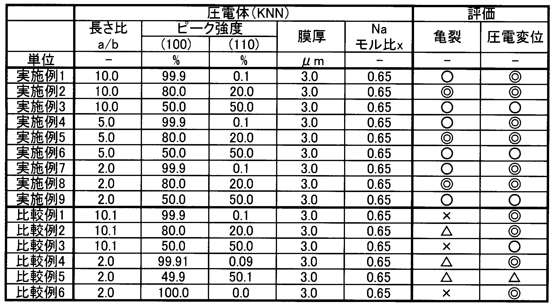
表1より、比較例1~3では、亀裂を抑制する効果が得られていない。これは、比較例1~3では、比a/bが10.0よりも大きく、(110)配向を(100)配向に混ぜることによって亀裂を抑制することができないほど、KNN薄膜が元々亀裂の入りやすい形状(細長い形状)であったためと考えられる。
また、比較例4でも、亀裂を抑制する効果が得られていない。これは、比較例4では、KNNの(110)配向度が0.1%未満であり、(100)配向に起因する内部応力を、(110)配向に起因する内部応力で十分に拡散しきれなかった結果、(100)配向に起因する内部応力によってKNN薄膜に亀裂が生じたものと考えられる。
また、比較例5でも、亀裂を抑制する効果が得られていない。これは、比較例5では、KNNの(110)配向度が50%を上回っていることから、(110)配向に起因する内部応力が増大しすぎて、上記内部応力による亀裂が生じているためと考えられる。さらに、比較例5では、圧電変位も小さいが、これは、KNNの(100)配向度が50%を下回っていることで、(100)配向による圧電変位の向上の効果が得られていないためと考えられる。
比較例6では、KNNは、(100)配向度が100%であり、(110)配向を有していないため、(100)配向に起因する内部応力を、(110)配向に起因する内部応力で拡散することができず、その結果、亀裂が生じているものと考えられる。
これに対して、実施例1~9では、KNN薄膜における長さの比a/bが2.0以上10.0以下であり、KNNの(100)配向度が50%以上100%未満であり、(110)配向度が0.1%以上50%以下である。このように、長方形状のKNN薄膜において、(100)配向度と(110)配向度とを適切に設定しているため、KNN薄膜が亀裂の生じやすい長方形状であっても、駆動時に(100)配向に起因する内部応力を(110)配向に起因する内部応力で拡散して、亀裂の発生を抑えることができ、また、(100)主配向によって良好な圧電変位が得られているものと考えられる。
特に、実施例1~3の結果より、KNNの(110)配向度が0.1%以上20%以下であれば、(100)配向度が80%以上となるため、(100)配向による良好な圧電変位を得ることができると言える。この点は、実施例4~6、実施例7~9の結果からも同様に言える。
なお、比a/b以外は比較例4と同様の条件とし、比a/bが1.9であるKNN薄膜を成膜して上記と同様の駆動を行ったところ、亀裂の発生は見られなかった。これは、比a/bが2.0未満であり、KNN薄膜がそもそも亀裂の生じにくい形状となるため、(110)配向が0.1%未満でも、亀裂を抑えることができているものと考えられる。
(実施例10~12)
次に、KNN薄膜を、膜厚が表2に示す値となるように成膜した以外は、実施例1と同様にして、実施例10~12の素子を作製し、実施例1と同様の評価方法で、圧電変位および亀裂について評価した。
次に、KNN薄膜を、膜厚が表2に示す値となるように成膜した以外は、実施例1と同様にして、実施例10~12の素子を作製し、実施例1と同様の評価方法で、圧電変位および亀裂について評価した。
表2は、実施例10~12における各パラメータと、圧電変位および亀裂の評価結果とを示している。

表2より、KNN薄膜の膜厚が10.1μmである実施例10についても、膜厚が0.5~10.0μmである実施例11~12についても、(110)配向を有しているため、亀裂が抑制されていることがわかる。これらの実施例10~12では、亀裂の評価は全て同じになっているが、KNN薄膜の膜厚が薄いほど、駆動時に亀裂が生じやすくなると考えられる。例えば比較例6では、(110)配向を有さず、膜厚が3.0μmと薄く形成されているため亀裂が生じていることがわかる。このことから、実施例11および実施例12のように膜厚が薄い構成の場合、(100)配向に(110)配向を混ぜることによって亀裂を抑える構成が非常に有効であると言える。
(実施例13~16)
次に、KNN薄膜を、Naの比率xが表3に示す値となるように、成膜条件を変更して成膜した以外は、実施例4と同様にして、実施例13~16の圧電素子付きの基板を作製した。そして、実施例13~16の上記基板を10個ずつ作製し、実施例1と同様の評価方法で、圧電変位および亀裂について評価した。
次に、KNN薄膜を、Naの比率xが表3に示す値となるように、成膜条件を変更して成膜した以外は、実施例4と同様にして、実施例13~16の圧電素子付きの基板を作製した。そして、実施例13~16の上記基板を10個ずつ作製し、実施例1と同様の評価方法で、圧電変位および亀裂について評価した。
表3は、実施例13~16における各パラメータと、圧電変位および亀裂の評価結果とを示している。
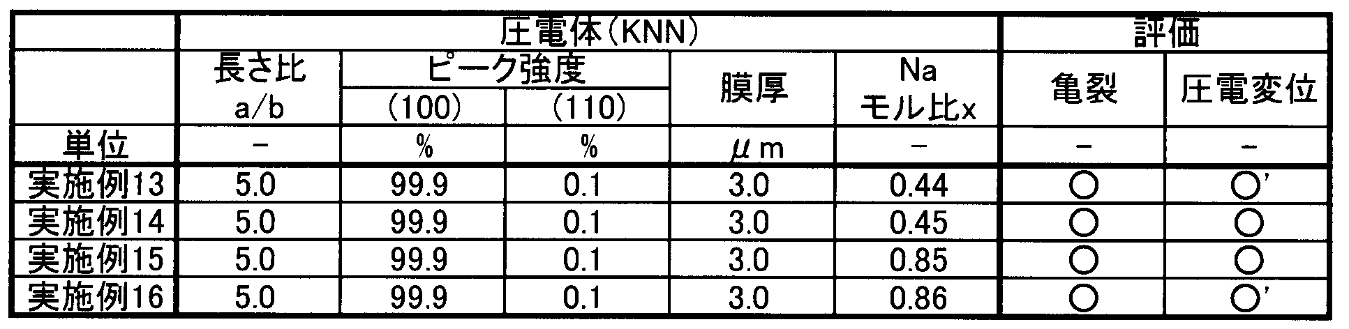
表3より、Naの比率xが0.45~0.85である実施例14および15では、圧電変位が良好であるのに対して、Naの比率xが上記範囲を外れた実施例13および16では、圧電変位の評価が実施例14および15よりも1ランク下がっている。このことから、0.45≦x≦0.85であれば、良好な圧電変位を得ることができると言える。特に、実施例14のx=0.45と実施例4のx=0.65との間(x=0.55)と、実施例4のx=0.65と実施例15のx=0.85との間(x=0.75)に、圧電変位の評価結果の◎と○の境界があると考えられることから、0.55≦x≦0.75であれば、さらに良好な圧電変位を得ることが期待できると言える。
なお、上述した各実施例では、KNNに添加物を添加していない例について説明したが、Ti、Ta、Ba、Ca、Liなどの添加物をKNNに添加しても、添加物の原子数濃度が5%以下であれば、上述した各実施例と同様の効果が得られることがわかった。
〔その他〕
以上で説明した本実施形態のインクジェットヘッドおよびインクジェットプリンタは、以下のように表現することもでき、これによって以下の作用効果を奏する。
以上で説明した本実施形態のインクジェットヘッドおよびインクジェットプリンタは、以下のように表現することもでき、これによって以下の作用効果を奏する。
本実施形態のインクジェットヘッドは、圧電体と、ノズルから吐出するインクを貯留する圧力室と、前記圧力室を構成する壁の一部であり、前記圧電体の変位により発生した圧力を前記インクに対して付与する振動板とを備えたインクジェットヘッドであって、前記圧電体が変位する駆動領域において、前記圧電体の厚さ方向に垂直な面内での長手方向の長さaと短手方向の長さbとの比a/bが、2.0以上10.0以下であり、前記圧電体は、ニオブ酸カリウムナトリウムを含み、前記圧電体において、X線回折によって得られるペロブスカイト相の(100)配向、(110)配向、(111)配向の各ピーク強度の総和に対する、(100)配向のピーク強度の割合が、50%以上100%未満であり、かつ、前記総和に対する(110)配向のピーク強度の割合が、0.1%以上50%以下である。
圧電体は、ニオブ酸カリウムナトリウム(KNN)を含んで構成されている。圧電体が変位する駆動領域の長さの比a/bが、2.0以上10.0以下であることにより、圧電体(駆動領域)は、平面視で(厚さ方向に垂直な面内で)長方形状に形成される。上記圧電体は、X線回折による(100)配向のピーク強度の割合が50%以上であり、(100)主配向であるため、良好な圧電変位を得ることができる。しかも、上記圧電体は、(110)配向のピーク強度の割合が、0.1%以上50%以下であり、(110)配向を含むため、(100)配向に起因する内部応力によって長方形状の圧電体に亀裂が生じるのを抑えることができる。その理由は、(100)配向に起因する内部応力が、(110)配向に起因する内部応力で拡散されるためと推測している。
上記インクジェットヘッドは、前記圧電体の一方の側および他方の側に、上部電極および下部電極をさらに備えており、前記駆動領域は、前記圧電体において前記上部電極と前記下部電極とで挟まれた領域であってもよい。この場合、上部電極と下部電極との間に電位差を付与することにより、圧電体を駆動領域において確実に変位(伸縮)させることができる。
前記圧電体の厚みは、0.5μm以上10μm以下であってもよい。圧電体が厚み0.5μm以上10μm以下の薄膜(圧電薄膜)になると、圧電体の駆動時に、応力集中によって長方形状の圧電体に亀裂がより生じやすくなる。このため、圧電体に亀裂が生じるのを抑えるべく、圧電体の配向性を上述のように設定する構成が非常に有効となる。
前記ニオブ酸カリウムナトリウムにおいて、カリウムとナトリウムとの原子数濃度の総和に対するナトリウムの原子数濃度の比率をxとしたとき、
0.45≦x≦0.85
であることが望ましい。xが上記範囲内であると、カリウムとナトリウムとが適切な原子数濃度の比率で圧電体に含まれるため、良好な圧電変位を実現することができる。特に、0.55≦x≦0.75であれば、カリウムとナトリウムとの含有量のバランスがさらに良好となるため、さらに良好な圧電変位の実現が期待できる。
0.45≦x≦0.85
であることが望ましい。xが上記範囲内であると、カリウムとナトリウムとが適切な原子数濃度の比率で圧電体に含まれるため、良好な圧電変位を実現することができる。特に、0.55≦x≦0.75であれば、カリウムとナトリウムとの含有量のバランスがさらに良好となるため、さらに良好な圧電変位の実現が期待できる。
前記圧電体において、前記総和に対する(110)配向のピーク強度の割合が、0.1%以上20%以下であることが望ましい。この場合、圧電体の(100)配向度を80%以上と高めることができるため、さらに良好な圧電変位を実現することができる。
本発明の他の側面に係るインクジェットプリンタは、上述したインクジェットヘッドを備え、前記インクジェットヘッドから記録媒体に向けてインクを吐出させる。上述したインクジェットヘッドの構成によれば、圧電体の亀裂の発生が抑えられるとともに、良好な圧電変位が得られるため、インクの吐出特性が良好で、信頼性の高いインクジェットプリンタを実現することができる。
本発明のインクジェットヘッドは、インクジェットプリンタに利用可能である。
1 インクジェットプリンタ
2 インクジェットヘッド
21a 圧力室
21d 振動板
32 圧電体
32a 駆動領域
2 インクジェットヘッド
21a 圧力室
21d 振動板
32 圧電体
32a 駆動領域
Claims (7)
- 圧電体と、
ノズルから吐出するインクを貯留する圧力室と、
前記圧力室を構成する壁の一部であり、前記圧電体の変位により発生した圧力を前記インクに対して付与する振動板とを備えたインクジェットヘッドであって、
前記圧電体が変位する駆動領域において、前記圧電体の厚さ方向に垂直な面内での長手方向の長さaと短手方向の長さbとの比a/bが、2.0以上10.0以下であり、
前記圧電体は、ニオブ酸カリウムナトリウムを含み、
前記圧電体において、X線回折によって得られるペロブスカイト相の(100)配向、(110)配向、(111)配向の各ピーク強度の総和に対する、(100)配向のピーク強度の割合が、50%以上100%未満であり、かつ、前記総和に対する(110)配向のピーク強度の割合が、0.1%以上50%以下であることを特徴とするインクジェットヘッド。 - 前記圧電体の一方の側および他方の側に、上部電極および下部電極をさらに備えており、
前記駆動領域は、前記圧電体において前記上部電極と前記下部電極とで挟まれた領域であることを特徴とする請求項1に記載のインクジェットヘッド。 - 前記圧電体の厚みは、0.5μm以上10μm以下であることを特徴とする請求項1または2に記載のインクジェットヘッド。
- 前記ニオブ酸カリウムナトリウムにおいて、カリウムとナトリウムとの原子数濃度の総和に対するナトリウムの原子数濃度の比率をxとしたとき、
0.45≦x≦0.85
であることを特徴とする請求項1から3のいずれかに記載のインクジェットヘッド。 - 0.55≦x≦0.75
であることを特徴とする請求項4に記載のインクジェットヘッド。 - 前記圧電体において、前記総和に対する(110)配向のピーク強度の割合が、0.1%以上20%以下であることを特徴とする請求項1から5のいずれかに記載のインクジェットヘッド。
- 請求項1から6のいずれかに記載のインクジェットヘッドを備え、前記インクジェットヘッドから記録媒体に向けてインクを吐出させることを特徴とするインクジェットプリンタ。
Applications Claiming Priority (2)
| Application Number | Priority Date | Filing Date | Title |
|---|---|---|---|
| JP2016065057 | 2016-03-29 | ||
| JP2016-065057 | 2016-03-29 |
Publications (1)
| Publication Number | Publication Date |
|---|---|
| WO2017169470A1 true WO2017169470A1 (ja) | 2017-10-05 |
Family
ID=59964116
Family Applications (1)
| Application Number | Title | Priority Date | Filing Date |
|---|---|---|---|
| PCT/JP2017/007899 Ceased WO2017169470A1 (ja) | 2016-03-29 | 2017-02-28 | インクジェットヘッドおよびインクジェットプリンタ |
Country Status (1)
| Country | Link |
|---|---|
| WO (1) | WO2017169470A1 (ja) |
Citations (2)
| Publication number | Priority date | Publication date | Assignee | Title |
|---|---|---|---|---|
| JP2012139919A (ja) * | 2010-12-28 | 2012-07-26 | Seiko Epson Corp | 液体噴射ヘッドの製造方法、液体噴射装置、及び圧電素子の製造方法 |
| JP2013197553A (ja) * | 2012-03-22 | 2013-09-30 | Hitachi Cable Ltd | 圧電体膜付き基板、圧電体膜素子及びその製造方法 |
-
2017
- 2017-02-28 WO PCT/JP2017/007899 patent/WO2017169470A1/ja not_active Ceased
Patent Citations (2)
| Publication number | Priority date | Publication date | Assignee | Title |
|---|---|---|---|---|
| JP2012139919A (ja) * | 2010-12-28 | 2012-07-26 | Seiko Epson Corp | 液体噴射ヘッドの製造方法、液体噴射装置、及び圧電素子の製造方法 |
| JP2013197553A (ja) * | 2012-03-22 | 2013-09-30 | Hitachi Cable Ltd | 圧電体膜付き基板、圧電体膜素子及びその製造方法 |
Similar Documents
| Publication | Publication Date | Title |
|---|---|---|
| US10639890B2 (en) | Inkjet head and method of manufacturing the same, and inkjet recording apparatus | |
| US8713768B2 (en) | Method of producing piezoelectric actuator | |
| JP6699662B2 (ja) | 圧電薄膜、圧電アクチュエータ、インクジェットヘッド、インクジェットプリンタおよび圧電アクチュエータの製造方法 | |
| CN105659401B (zh) | 压电元件、喷墨头、喷墨打印机以及压电元件的制造方法 | |
| WO2016093078A1 (ja) | 圧電アクチュエータ、圧電アクチュエータの製造方法、液滴吐出ヘッド、液滴吐出ヘッドの製造方法、液滴吐出装置および液滴吐出装置の製造方法 | |
| JP6281629B2 (ja) | 圧電薄膜付き基板、圧電アクチュエータ、インクジェットヘッド、インクジェットプリンタおよび強誘電体薄膜の製造方法 | |
| JP6048306B2 (ja) | インクジェットヘッドおよびその駆動方法と、インクジェットプリンタ | |
| JP2017065138A (ja) | インクジェット駆動装置 | |
| JP6481686B2 (ja) | 強誘電体薄膜、圧電薄膜付き基板、圧電アクチュエータ、インクジェットヘッドおよびインクジェットプリンタ | |
| JP5736829B2 (ja) | 電気機械変換素子の製造方法、この製造方法により製造された電気機械変換素子、及びこれを用いたインクジェットヘッド並びにインクジェット記録装置 | |
| WO2017169470A1 (ja) | インクジェットヘッドおよびインクジェットプリンタ | |
| JP6365347B2 (ja) | 圧電デバイス、圧電デバイスの製造方法、インクジェットヘッド、インクジェットヘッドの製造方法およびインクジェットプリンタ | |
| JP6274308B2 (ja) | 圧電素子、圧電素子の製造方法、圧電アクチュエータ、インクジェットヘッドおよびインクジェットプリンタ | |
| JP6311718B2 (ja) | 圧電アクチュエータの製造方法 | |
| WO2015182228A1 (ja) | 圧電アクチュエータ、圧電アクチュエータの製造方法、インクジェットヘッドおよびインクジェットプリンタ | |
| JP2016115702A (ja) | 圧電アクチュエータ、圧電アクチュエータの製造方法、インクジェットヘッドおよびインクジェットプリンタ | |
| JP5857548B2 (ja) | 薄膜製造方法、電気機械変換素子の製造方法及び液体吐出ヘッドの製造方法 | |
| WO2017090445A1 (ja) | 圧電素子、圧電素子の製造方法、圧電アクチュエータ、インクジェットヘッドおよびインクジェットプリンタ | |
| JP2015214127A (ja) | インクジェットヘッドおよびその製造方法と、インクジェットプリンタ | |
| JP6468881B2 (ja) | 圧電薄膜、圧電薄膜の製造方法、圧電薄膜付き基板、圧電アクチュエータ、圧電センサ、インクジェットヘッドおよびインクジェットプリンタ | |
| JP2017024293A (ja) | インクジェットヘッド、インクジェットヘッドの製造方法およびインクジェットプリンタ | |
| JP4802836B2 (ja) | 液体噴射ヘッドの製造方法 | |
| JP2016107476A (ja) | インクジェットヘッドおよびインクジェットプリンタ | |
| JP2014179485A (ja) | アクチュエータ素子及び液滴吐出ヘッド及び画像形成装置 |
Legal Events
| Date | Code | Title | Description |
|---|---|---|---|
| NENP | Non-entry into the national phase |
Ref country code: DE |
|
| 121 | Ep: the epo has been informed by wipo that ep was designated in this application |
Ref document number: 17774015 Country of ref document: EP Kind code of ref document: A1 |
|
| 122 | Ep: pct application non-entry in european phase |
Ref document number: 17774015 Country of ref document: EP Kind code of ref document: A1 |
|
| NENP | Non-entry into the national phase |
Ref country code: JP |