WO2017169101A1 - ライトガイド、ライトガイドを備えた検出器、及び荷電粒子線装置 - Google Patents
ライトガイド、ライトガイドを備えた検出器、及び荷電粒子線装置 Download PDFInfo
- Publication number
- WO2017169101A1 WO2017169101A1 PCT/JP2017/003884 JP2017003884W WO2017169101A1 WO 2017169101 A1 WO2017169101 A1 WO 2017169101A1 JP 2017003884 W JP2017003884 W JP 2017003884W WO 2017169101 A1 WO2017169101 A1 WO 2017169101A1
- Authority
- WO
- WIPO (PCT)
- Prior art keywords
- light
- scintillator
- light guide
- incident
- charged particle
- Prior art date
- Legal status (The legal status is an assumption and is not a legal conclusion. Google has not performed a legal analysis and makes no representation as to the accuracy of the status listed.)
- Ceased
Links
Images





Classifications
-
- G—PHYSICS
- G01—MEASURING; TESTING
- G01T—MEASUREMENT OF NUCLEAR OR X-RADIATION
- G01T1/00—Measuring X-radiation, gamma radiation, corpuscular radiation, or cosmic radiation
- G01T1/16—Measuring radiation intensity
- G01T1/20—Measuring radiation intensity with scintillation detectors
-
- H—ELECTRICITY
- H01—ELECTRIC ELEMENTS
- H01J—ELECTRIC DISCHARGE TUBES OR DISCHARGE LAMPS
- H01J37/00—Discharge tubes with provision for introducing objects or material to be exposed to the discharge, e.g. for the purpose of examination or processing thereof
- H01J37/02—Details
- H01J37/244—Detectors; Associated components or circuits therefor
-
- H—ELECTRICITY
- H01—ELECTRIC ELEMENTS
- H01J—ELECTRIC DISCHARGE TUBES OR DISCHARGE LAMPS
- H01J37/00—Discharge tubes with provision for introducing objects or material to be exposed to the discharge, e.g. for the purpose of examination or processing thereof
- H01J37/26—Electron or ion microscopes; Electron or ion diffraction tubes
- H01J37/28—Electron or ion microscopes; Electron or ion diffraction tubes with scanning beams
-
- H—ELECTRICITY
- H01—ELECTRIC ELEMENTS
- H01J—ELECTRIC DISCHARGE TUBES OR DISCHARGE LAMPS
- H01J2237/00—Discharge tubes exposing object to beam, e.g. for analysis treatment, etching, imaging
- H01J2237/244—Detection characterized by the detecting means
- H01J2237/2443—Scintillation detectors
-
- H—ELECTRICITY
- H01—ELECTRIC ELEMENTS
- H01J—ELECTRIC DISCHARGE TUBES OR DISCHARGE LAMPS
- H01J2237/00—Discharge tubes exposing object to beam, e.g. for analysis treatment, etching, imaging
- H01J2237/244—Detection characterized by the detecting means
- H01J2237/2445—Photon detectors for X-rays, light, e.g. photomultipliers
Definitions
- the present invention relates to a light guide, a detector provided with a light guide, and a charged particle beam apparatus, and more particularly, a light guide for guiding light to a light receiving element with high efficiency, a detector provided with the light guide, and a charged particle beam. Relates to the device.
- a charged particle beam apparatus that detects charged particles obtained by irradiating a sample with a charged particle beam such as an electron beam is provided with a detector for detecting charged particles. For example, when electrons emitted from a sample are detected by scanning the sample with an electron beam, a positive voltage of about 10 kV is applied to the electron detector to guide the electrons to the scintillator of the charged particle detector. The light generated in the scintillator by the collision of electrons is guided to the light guide, converted into an electric signal by a light receiving element such as a photoelectric tube, and becomes an image signal or a waveform signal.
- a light receiving element such as a photoelectric tube
- Patent Document 1 describes a light guide attached to a scintillator. Further, Patent Document 1 describes a configuration in which an inclined surface is provided on a light guide so as to guide light emitted from a scintillator to a PMT (Photomultiplier Tube). Patent Document 2 describes a light guide using a highly transparent material such as an acrylic resin. Further, Cited Document 2 shows a device that guides light generated by a scintillator by a light guide and makes it incident on a photoelectric conversion element such as a photomultiplier tube or a semiconductor light receiving element. In addition, a scintillator structure is described in which a surface opposite to the electron incident surface is inclined to guide light toward the light guide with high efficiency.
- the light generated by the scintillator is guided to the light receiving element by the light guide, but there is light that collides with the light guide wall surface in the process of reaching the light receiving element.
- the collided light travels toward the light receiving element by reflection, but there is also light that penetrates outside the light guide. If the light can be guided to the light receiving element while suppressing the transmission of light to the outside of the light guide, the SN of the charged particle beam apparatus can be improved.
- the light generated by the scintillator can be guided to the PMT by reflecting the light generated by the scintillator by the slope opposite to the scintillator mounting surface of the light guide.
- the relative angle between the inclined surface opposite to the scintillator mounting surface and the mounting surface may be increased. It is conceivable that the dimension in the optical axis direction of an electron microscope or the like becomes large and is not suitable as a member disposed in a limited space in the vacuum chamber.
- the light emitted from the side of the scintillator can be guided to the light receiving element, but the light is transmitted from the surface opposite to the collision surface of the charged particle of the scintillator. After all, there is a limit to high-efficiency detection.
- a light guide that aims to guide light generated by the scintillator to the light receiving element with high efficiency, a detector equipped with the light guide, and a charged particle beam device.
- a light guide that guides light generated from the scintillator to a light receiving element below, the first surface facing the surface opposite to the charged particle incident surface of the scintillator, A scintillator accommodating portion formed from a second surface facing a surface different from the surface opposite to the surface opposite to the charged particle incident surface of the scintillator, and reflecting light incident from the second surface toward the inside of the light guide
- a light guide with an inclined surface We propose a light guide with an inclined surface.
- the detector includes a scintillator and a light guide that guides light generated from the scintillator to a light receiving element, and the light guide includes charged particles of the scintillator.
- a concave portion formed by a first surface facing a surface opposite to the incident surface, a second surface facing a surface different from the surface opposite to the charged particle incident surface of the scintillator, and the second surface
- the detector is provided with an inclined surface that reflects the light incident from the inside toward the inside of the light guide, and the scintillator is accommodated in the concave portion.
- a charged particle beam apparatus including a detector that detects at least one of charged particles generated by the scintillator, the detector having a scintillator and a light guide that guides light generated from the scintillator to a light receiving element;
- the light guide is formed of a first surface facing a surface opposite to the charged particle incident surface of the scintillator and a second surface facing a surface different from the surface opposite to the charged particle incident surface of the scintillator.
- the concave portion is configured to reflect light incident from the second surface toward the inside of the light guide.
- the light generated by the scintillator can be guided to the light receiving element with high efficiency.
- the figure which shows the example which fitted the cross-sectional shape of the bending part using the equation of a circle The figure explaining the specific shape of a light guide.
- a solid scintillator has a plurality of surfaces and emits light from the surface of all scintillators that do not have a reflecting material that reflects light, but guides light emitted from the scintillator surface that does not face the light guide. It is not possible. That is, only light emitted from a part of the surface can enter the light guide. Further, when the light guide is not a straight line and has a bent portion, light leaks at the bent portion and does not reach the light receiving element.
- an optical system using a light guide often has a low ratio (light utilization efficiency) of light reaching the light receiving element with respect to light emitted from the scintillator.
- a charged particle beam apparatus including a detector having a scintillator as a detection element and a light guide between the scintillator and the light receiving element will be described.
- an example of an electron microscope particularly a scanning electron microscope will be described.
- the present invention is not limited to this example, and the embodiment described below is not limited to a scanning ion microscope using an ion beam.
- Application to a charged particle beam apparatus is also possible.
- the present invention is also applicable to a semiconductor pattern measuring device, inspection device, observation device, etc. using a scanning electron microscope.
- a scintillator refers to an element that emits light upon incidence of a charged particle beam.
- the scintillators in this specification are not limited to those shown in the embodiments, and can take various shapes and structures.
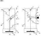
- FIG. 1 is a diagram showing a basic configuration of the electron microscope 1.
- FIG. 1 is a side view of the electron microscope, and
- FIGS. 2 and 3 are detailed views of the scintillator 5 and the light guide 3.
- the primary electron beam 100 emitted from the electron source 2 is irradiated onto the sample 50, and secondary particles 101 such as secondary electrons and reflected electrons are emitted.
- the secondary particles 101 collide with the signal particle limiting plate 6 and then enter the scintillator 5.
- limiting board 6 may be called a tertiary particle
- released from the sample are carried out.
- the secondary particles including secondary electrons generated by colliding with the signal particle restricting plate 6 are referred to as secondary particles.
- a scintillator 5 having a circular secondary particle incident surface will be described.
- a cylindrical scintillator whose dimension in the height direction is relatively small relative to the size of the incident surface of the secondary particles will be described as an example.
- the scintillator 5 Light emitted from the scintillator 5 is guided by the light guide 3 and converted into an electric signal by the light receiving element 4.
- the scintillator 5, the light guide 3, and the light receiving element 4 may be collectively referred to as a detection system.
- a signal obtained by the light receiving element 4 is stored in a storage medium such as a frame memory in synchronization with scanning of a primary electron beam (electron beam).
- a contrast image of the scanning region can be obtained by displaying the luminance corresponding to the obtained signal amount at the image position (pixel) corresponding to the electron beam irradiation position.
- illustration of an electron optical system for focusing and irradiating the sample with the primary electron beam 100 that is, a deflector, a lens, a diaphragm, an objective lens, and the like is omitted.
- the inside of the electron optical column 60 constituting the electron optical system is maintained in a vacuum state, and is configured such that the beam passes through the vacuum space.
- the sample 50 is placed on a sample stage that moves the sample in at least the XY direction (when the ideal optical axis of the primary electron beam is the Z direction).
- the sample 50 and the sample stage are arranged in the sample chamber 61. Is done.
- the sample chamber 61 is generally kept in a vacuum state during electron beam irradiation.
- the electron microscope includes a control unit that controls the operation of the whole and each component, a display unit that displays an image, an input unit through which a user inputs an operation instruction for the electron microscope, and the like.
- a negative voltage application power source (not shown) is connected to the sample stage, and a deceleration electric field for the electron beam can be formed.
- the decelerating electric field for the electron beam becomes an accelerating electric field for secondary particles (secondary electrons and backscattered electrons) emitted from the sample, so that the secondary particles and the like are accelerated toward the electron source 2 to generate signal electrons. Collides with the limiting plate 6 or the like.
- This electron microscope is an example of the configuration, and other configurations can be applied as long as the electron microscope includes the scintillator 5, the light guide 3, and the light receiving element 4.
- the electron microscope includes the scintillator 5, the light guide 3, and the light receiving element 4.
- FIG. 1 an example is described in which new secondary particles (tertiary particles) generated based on the collision of secondary particles with the signal electron limiting plate 6 are detected.
- a scintillator may be arranged so that light generated by the scintillator is guided to the light receiving element by a light guide.
- the secondary particles 101 include transmission electrons, scanning transmission electrons, and the like.
- only one detector is shown, but a plurality of detectors may be provided.
- the backscattered electron detection detector and the secondary electron detection detector may be provided separately, or a plurality of detectors may be provided to discriminate and detect the azimuth angle or elevation angle.
- the front direction DF is parallel to the normal line of the bottom surface of the cylindrical scintillator 5 (referred to as the upper bottom surface 5c in order to distinguish the upper and lower bottom surfaces of the cylinder), and the secondary particles 101 propagate. It is a direction to come.
- the side surface direction DS is a direction perpendicular to the front surface direction DF.
- the figure is a view of the cylindrical scintillator 5 viewed from the side surface direction DS.
- the scintillator 5 includes a light emitting unit 5 a that emits light by converting the energy of the incident secondary particles 101 into light, and a conductive layer 5 b that applies a voltage to the scintillator 5.
- the conductive layer 5b is a layer formed on the light emitting portion 5a and is an Al layer in the present embodiment.
- the scintillator 5 is not limited to this configuration as long as it has the light emitting portion 5a.
- a semiconductor As a material of the light emitting portion 5a, a semiconductor (GaN, Si, SiC), ceramic phosphor YAG (Y 3 Al 5 O 12 : Ce), YAP (YAlO 4: Ce), used was deposited on a substrate such as a glass
- a powder phosphor Y2SiO5: Ce As an example of the semiconductor scintillator, there is a semiconductor that uses a structure in which a quantum well is formed by stacking InGanN and GaN as a light conversion unit. The InGanN layer and the GaN layer are stacked in the incident direction of the charged particles.
- the secondary particles 101 incident on the scintillator 5 pass through the conductive layer 5b and are converted into light by the light emitting unit 5a.
- the converted light propagates through the light emitting unit 5a and is emitted to the outside of the scintillator 5. Since the conductive layer 5b functions as a reflecting member for light, light is emitted from all surfaces where the conductive layer 5b is not provided.
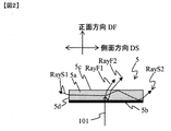
- Examples of light rays are shown as RayF1, RayF2, RayS1, and RayS2 in the figure.
- RayF1 and F2 are examples in which the light is emitted from the upper and lower surfaces 5c in the front direction DF, and RayF2 is an example in which the light is reflected by the conductive layer 5b and emitted.
- RayS1 and RayS2 are examples in which the light propagates in the side surface direction DS and exits from the side surface 5d.
- RayS2 shows an example in which the light is totally reflected by the upper bottom surface 5c, reflected by the conductive layer 5b, and emitted from the side surface 5d, and is an example in which the inside of the light emitting portion 5a is guided and emitted from the side surface 5d. Since the light emitting part 5a has a higher refractive index than air, a part of the light is totally reflected on the surface of the scintillator 5 and guided.
- the ratio of the total light emitted from the side surface 5d (side emission light amount Is) and the total light emitted from the upper bottom surface 5c (planar emission light amount Ip) depends on the internal structure of the scintillator 5.
- the refractive index of the material is generally larger than 1.5.
- the total reflection angle on the surface of the scintillator 5 when the refractive index is 1.5 is about 40 degrees. Therefore, about 75% or more of the light incident on the surface is totally reflected.
- the inside of the light emitting portion 5a has a structure in which scattering is likely to occur, it may diffusely reflect and reach the surface again and exit from the surface.
- light scattering hardly occurs. The light is guided to a large amount, and a lot of light is emitted from the side surface 5d.
- the height of the cylinder is 0.5 mm
- the diameter of the circle is 9 mm
- Ip: Is 1: 1.
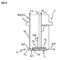
- FIG. 3 is a cross-sectional view of the light guide 3, and the light guide 3 has a rotationally symmetric shape with respect to the center line CL.
- the material of the light guide 3 PMMA resin, cycloolefin polymer (COP) resin, silica, quartz, or the like may be used.
- COP cycloolefin polymer
- silica silica
- quartz or the like
- the present invention is not limited to materials.
- a separation flange 3c for separating the vacuum inside the electron optical column 60 and the outside atmosphere is provided on the side surface 3d of the light guide cylinder.
- the separation flange 3c may or may not depend on the structure of the electron microscope 1.
- the light receiving element 4 is disposed outside the electron optical column 60 and the scintillator 5 is disposed inside the electron optical column 60, so that the light guide 3 is provided with a separation flange 3c. .
- the light exit surface 3 b of the light guide 3 is circular and is a surface disposed facing the light receiving element 4.
- the surface facing the upper bottom surface 5 c of the scintillator 5 is the incident surface 3 a (first surface) of the light guide 3.
- a part of the light incident from the incident surface 3a is absorbed by the light guide 3, but most of the light reaches the output surface 3b.
- RayF3 is an example of a light beam that enters the light guide from the incident surface 3a and exits from the output surface 3b.
- a part of the scintillator 5 that is disposed to face the side surface 5d is a side prism 3e.
- the side prism 3e is opposed to the side surface 5d of the scintillator 5, and receives a side prism incidence surface 3e1 (first surface) that receives light from the side surface 5d. 2 planes).
- the side prism incident surface 3e1 is a side wall surface having a surface direction in a direction different from the incident surface 3a of the light guide 3.
- the incident surface 3 a and the side prism incident surface 3 e 1 of the light guide 3 form a housing space surrounding the scintillator 5.
- the accommodation space is formed so as to face all of the surface from which the light of the scintillator 5 is emitted.
- the housing space has a configuration in which a surface facing only a part of the surface from which the light of the scintillator 5 emits is formed, the use space has an effect of improving the light utilization efficiency. .
- the side prism 3e has a reflecting surface 3e2 (an inclined surface) that reflects the light incident from the side prism incident surface 3e1 so that the light is directed toward the output surface 3b.
- the reflecting surface 3e2 is formed so as to surround the side prism incident surface 3e1.
- RayS3 is an example of a light ray that enters the side prism 3e from the incident surface 3e1, is totally reflected by the reflecting surface 3e2, and is emitted from the exit surface 3b.
- the reflecting surface 3e2 has a normal angle 3eN of the side prism incident surface 3e1 and a predetermined angle ⁇ e2 so that light incident in the normal direction 3eN of the side prism incident surface 3e1 can be totally reflected. It is a configuration.
- the total reflection occurs only when the incident angle of light on the reflecting surfaces 3e2 is larger than the critical angle theta c.
- Incident light also has light at angles other than the normal direction 3eN, and in order to reflect more light, it is better to provide a reflecting member on the surface of the reflecting surface 3e2.
- the reflective member include aluminum, silver, and a multilayer reflective film.
- the angle ⁇ e2 from the viewpoint of reflection in the direction of the exit surface 3b, it is better to be larger than 20 degrees and smaller than 70 degrees.
- the upper limit of the angle depends on the shape of the light guide 3.
- the bent light guide 3 has a different value.
- the angle ⁇ e2 reflected in the normal direction 3aN of the incident surface 3a does not depend on the shape of the light guide 3 and is preferably in the range of 45 ° ⁇ 15 °. Since most of the light traveling in the normal direction 3aN of the incident surface 3a can be guided through the light guide 3 without leaking from other than the exit surface of the light guide 3, the light use efficiency can be improved. Play.
- the side prism 3e also causes the light emitted from the side surface 5d of the scintillator 5 to be incident on the light guide 3, reflected by the reflecting surface 3e2 toward the light emitting surface 3b, and propagating more light toward the light receiving element 4.
- the light use efficiency is improved.
- the dimension in the thickness direction of the surface (side surface) in the direction orthogonal to the incident surface is sufficiently smaller than the dimension in the surface direction of the incident surface of the charged particles.
- the light emitted from the upper bottom surface 5c is guided to the direction of the center line CL of the light guide (the optical path direction of the light guide) without being reflected using a prism or the like, and emitted from the side of the scintillator.
- the reflected light is configured to be guided in the light guide optical path direction with reflection using a side prism. That is, in the case where the accommodation space for the scintillator 5 is formed in the light guide 3, the height dimension of the side prism incident surface 3 e 1 is made smaller than the incident surface 3 a, and the side surface 5 d of the scintillator 5 and the side surface of the light guide 3 are configured.
- the prism incident surface 3e1, the upper bottom surface 5c of the scintillator, and the incident surface 3a of the light guide 3 are arranged to face each other.
- FIG. 4 is an enlarged cross-sectional view of the vicinity of the side prism 3e.
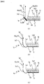
- FIG. 4A shows an example in which a reflective member 3e2R is attached to the surface of the reflective surface 3e2.
- the reflecting member 3e2R By providing the reflecting member 3e2R, it is possible to reflect light that cannot be totally reflected by the reflecting surface 3e2 and penetrates, and light utilization efficiency is improved.
- the light ray RayS4 is light that passes through the reflecting surface 3e2 and is lost when there is no reflecting member 3e2R. However, when there is the reflecting member 3e2R, it is reflected and guided toward the exit surface 3b.
- there are various methods of attachment such as vapor deposition, and this embodiment is not limited to the method of attachment.
- the entire light guide is not covered using the reflecting member, and is attached only to a part (reflecting surface) of the light guide. Since a general reflecting material absorbs a part of light at the time of reflection, it is not attached to the side surface 3d of the light guide where light is reflected a plurality of times.
- the absorption rate when a metal is used as the reflecting material is about 5 to 15%. It is important that the side surface 3d is guided by total reflection at which no light absorption occurs.
- FIG. 4B shows a case where the shape of the reflecting surface 3e2 is not a straight line but a broken line.
- the light propagation direction is changed by multiple reflections.
- a ray example RayS5 is illustrated.
- FIG. 4C shows a case where the shape of the reflecting surface 3e2 is not a straight line but a curved line.
- the light propagation direction is changed by multiple reflections.
- a ray example RayS6 is illustrated.
- Various shapes such as a circle, an ellipse, a parabola, and a hyperbola are conceivable.
- not only a curve but a combination of a curve and a broken line or a curve and a straight line may be used. If the shape of the reflection surface 3e2 is a shape that reflects light so as to propagate toward the emission surface 3b, the effect of improving the light utilization efficiency is achieved.
- FIG. 5A is a view of the electron microscope viewed from the side
- FIG. 5B is a view of the electron microscope 1 viewed from the direction of arrow A in FIG.
- FIG. 6A is a cross-sectional view of the light guide 3 in the plane S1 when the plane including the dotted line B and the center of the emission surface is the plane S1.
- the plane S1 is a plane including the center of the incident surface 3a.
- the light guide shape is different from the example of FIG. In the light guide 3 of this embodiment, the incident surface 3a and the exit surface 3b are not opposed (the scintillator has no exit surface in the normal direction of the entrance surface of the scintillator). Is provided.
- detection system For simplicity, only one detection system is shown, but a plurality of detection systems may be provided, or another detection system with a signal particle limiting plate may be provided. Although not shown in the present embodiment, another detection system having a signal particle restriction plate is provided on the side closer to the sample 50 than the illustrated detection system.
- the primary electron beam 100 emitted from the electron source 2 travels straight toward the sample 50, but the secondary particles 101 have an optical system that can bend toward the scintillator 5. Since the secondary particles 101 are directly incident on the scintillator 5, the secondary particles 101 that have traveled straight from the sample 50 can be detected with high sensitivity.
- the light guide 3 has a bent portion 3f, and light is also guided toward the light exit surface 3b while reflecting the bent portion 3f, and reaches the light receiving element 4.
- the cross-sectional shape will be described in detail with reference to FIG.
- the cross-sectional shape is large and consists of three parts. There are three portions: bent portions 3f1 and 3f2, inclined portions 3g1 and 3g2 whose shape changes more gently than the bent portions, and straight portions 3h1 and 3h2.
- the shape of the straight line portion 3h is a cylinder having an emission surface 3b as a bottom surface ( a circle with a radius ra, see FIG. 6B).
- a separation flange 3c is provided on the straight line portion 3h. By providing the separation flange 3c in the straight line portion 3h, the separation flange 3c can be pressed perpendicularly to the side wall of the electron optical column 60, and the structure prevents air from flowing into the vacuum.
- the shape of the inclined portion 3g is a shape connecting the bent portion 3f and the straight portion 3h.
- the cross-sectional shapes 3g1 and 3g2 are gently changing curves.
- the cross-sectional shape is not limited to a curved line, and may be a straight line, a broken line, a curved line and a straight line, or a combination of a curved line and a broken line.
- the cross-sectional shapes 3f1 and 3f2 of the bent portions are arcs having a central angle between 60 degrees and 89 degrees.
- the cross-sectional shape may be a curved line deviated from an arc, a part thereof may be an arc or a curve, and the other may be a straight line or a broken line.
- the bent portion has a complicated shape in order to reduce the amount of light leaking from the surface of the bent portion to the outside of the light guide.
- the incident surface 3a has the shape shown in FIG. 6C, and the cross-sectional shapes 3f1 and 3f2 are connected to the points D and E, respectively.
- the left half is a circle 3a1 and the right half is an ellipse 3a2.
- the radius of the circle is r a
- the minor axis of the ellipse half the length of the major axis are respectively r a and r b (r a ⁇ r b ).
- the center of the scintillator 5 is disposed at a position substantially opposite to the intersection of the dotted line F and the line segment connecting the points D and E.
- the cross-sectional shape of the light guide 3 in the plane S2 is the same circle as the emission surface 3b.
- the shape of the bent portion 3f is a shape obtained by connecting the shape of the circle and the incident surface 3a with the cross-sectional shapes 3f1 and 3f2 as outlines.
- the shape of the bent portion can be created by lofting the shape of the circle and the incident surface 3a with the cross-sectional shapes 3f1 and 3f2 as contours.
- FIG. 6D is a perspective view of the light guide 3 of the present embodiment.
- Reference numeral 3 i denotes a portion for fixing the light guide 3 and the scintillator 5.
- FIG. 7A is a cross-sectional view on the plane S1 for explaining the cause of light leakage at the bent portion 3f.
- the shapes of the entrance surface 3a and the exit surface 3b are circles shown in FIG. 6B, and the cross-sectional shapes 3f1 and 3f2 of the bent portions are arcs having a central angle of 90 degrees and starting from the entrance surface 3a.
- the bent portion 3f and the exit surface 3b are connected by a straight portion 3h. It is the simplest light guide shape that connects the entrance surface 3a and the exit surface 3b.
- the light beam path through which typical light leaks will be described using three light beam examples.
- the ray RayF5 is an example that reaches the cross section 3f1 of the bent portion and transmits through the surface because the angle with the normal 3N1 of the surface of the reaching point is smaller than the critical angle of total reflection. All the light beams whose angle of light ray exiting from the normal surface of the incident surface 3a and the light incident surface 3a is larger than the angle shown in the figure pass through the bent portion 3f and become a loss.
- a ray RayF6 (shown by a dotted line to distinguish it from other rays) is totally reflected in the normal direction of the incident surface 3a at the cross section 3f2 of the bent portion, reaches the cross section 3f1 of the bent portion, and reaches the surface of the reaching point.
- the angle with the normal line 3N2 is smaller than the critical angle of total reflection, and thus the surface is transmitted.
- the light emitted from the position close to the cross section 3f2 of the bent portion is reflected by the cross section 3f2 of the bent portion and leaks from the light guide 3 through the same light path.
- the ray RayF7 is inclined from the normal line of the incident surface 3a toward the exit surface 3b, and the light ray emitted from the incident surface 3a reaches the cross section 3h1 of the straight line portion, and is an angle with the normal line 3N3 of the surface of the arrival point Is smaller than the critical angle of total reflection.
- Light that reaches a surface having a normal line substantially parallel to the normal line of the incident surface 3a has a high probability of transmitting through the surface.
- the transmittance follows that of Fresnel.
- the light guide 3 shown in FIG. 6A has a shape that suppresses these light leaks.
- the light guide shown in FIG. 7B is the light guide 3 shown in FIG. 6A, and the light leakage suppression effect will be described with reference to FIG.
- the main features of the light guide 3 in FIG. 7B are that the radius of curvature of the cross section 3f1 of the bent portion is larger than that in FIG. 7A and the shape of the incident surface 3a is shown in FIG.
- the major axis is a shape including an ellipse in the direction of the exit surface.
- the surface of the light guide 3 that guides light to the exit surface 3b exists in addition to the region between the entrance surface 3a and the exit surface 3b.
- the region between the entrance surface 3a and the exit surface 3b is a region indicated by an arrow DA in FIG. 7B.
- a dotted line indicated by an arrow is an auxiliary line for indicating a region, and a lower dotted line in the figure coincides with an end portion of the incident surface 3a, and an upper dotted line coincides with an end portion of the emission surface 3b.
- the surface of the light guide 3 that guides light to the emission surface 3b does not exist outside the region.
- the fixing portion such as the separation flange 3c is not a surface for guiding light to the emission surface 3b.
- the ray RayF8 is a ray emitted from the incident surface 3a at the same angle as the ray RayF5, but the incident angle to the cross section 3f1 of the bent portion is larger than that of the ray RayF5 and is totally reflected. Since the radius of curvature is large, the normal 3N4 at the position where the light enters the arc enters the position greatly inclined from the normal of the incident surface 3a. Therefore, the amount of light totally reflected at the bent portion is increased, and the light use efficiency of the light guide is improved.
- the ray RayF10 is a ray emitted from the incident surface 3a at the same angle as the ray RayF7. Since the radius of curvature is large, the ray RayF10 is incident on the cross section 3f1 of the bent portion near the end point, and is totally reflected and guided. Since the normal 3N6 of the cross section 3f1 of the bent portion near the end point is inclined in the direction opposite to the exit surface 3b from the incident surface 3a, the angle between the normal 3N6 and the incident light beam is increased, and total reflection is easy. Since the Fresnel reflectivity is improved even when it is not totally reflected, the amount of reflected light is increased and the light utilization efficiency of the light guide is improved.
- the scintillator 5 is a cylinder with a diameter of 9 mm
- the incident surface 3a is a circle with a diameter of 10 mm
- the curvature radii of the cross sections 3f1 and 3f2 of the bent portion are changed from 15 mm, 5 mm to 18 mm, and 8 mm, respectively.
- the ray RayF9 is a ray emitted from the incident surface 3a at the same angle as the ray RayF6.
- a part of the entrance surface 3a is an ellipse whose major axis is in the direction of the exit surface, and the cross section 3f2 of the bent portion is moved to the exit surface 3b side, so that the ray RayF9 is reflected by the cross section 3f2 and is not reflected by the cross section 3f2. It is possible to reach 3g1.
- the ray RayF9 does not necessarily undergo total reflection at the cross-section 3g1, but the angle between the ray RayF9 and the normal 3N5 is larger at the incident point of the cross-section 3g1 than in the case of the ray RayF6.
- the amount of light to be guided is increased, and the light use efficiency is improved.
- the shape of the elliptical portion of the incident surface 3a will be described.
- r a and r b is, 4.5 mm respectively, when 5.5 mm
- the incidence surface 3a when a circle having a diameter of 9mm
- a part of the incident surface 3a is an ellipse, and the shape is elongated toward the exit surface to move the cross section 3f2 to the exit surface, thereby improving the light use efficiency.
- the shape may be elongated toward the exit surface.
- the distance from the center of the scintillator 5 to the end of the entrance surface 3a is different in the exit surface direction and the opposite direction, and the distance in the exit surface direction only needs to be long.
- the cross-sectional shape 3f1 of the bent portion is the arc shape of the present embodiment.
- the cross-sectional shape 3f1C (indicated by a dotted line) is such that the center CP1 of the arc exists in a plane SP (indicated by a dotted line) including the incident surface 3a, and the tangent rising from the incident surface 3a of the cross-sectional shape 3f1C is the normal line 3aN of the incident surface. It is a cross-sectional shape in the case of parallel.
- the cross-sectional shape 3f1C is the shape of the bent portion when the light guide without the inclined portion shown in FIG. 7A is configured, and can be said to be the simplest shape as the bent portion.
- the cross-sectional shape 3f1 is a configuration in which the center CP2 of the arc does not exist in the plane SP, and is below the incident surface 3a (in the direction away from the light guide 3). Furthermore, normal 3aN of the incident surface and the tangent 3f1T rising from the incident surface 3a of the cross-sectional shape 3f1 is a shape having a predetermined angle theta t.
- the angle ⁇ t is preferably in the range of about 2 degrees to 10 degrees from the viewpoint of improving the light utilization efficiency.
- the angle ⁇ t of the light guide 3 shown in FIG. 7B is 2.5 degrees.
- the distance between the center CP2 and the plane SP is 1 mm. The distance is preferably in the range of about 0.3 mm to 5 mm.
- the cross-sectional shape 3f1 is included in the outer curved surface starting from the end of the incident surface 3a, and the cross-sectional shape 3f2 is the inner curved surface. included.
- the configuration described above is a configuration in which the outer curved surface has a tangent line inclined toward the incident surface side from the normal line 3aN of the incident surface at the contact point between the outer curved surface and the incident surface 3a.
- the ray RayF11 is a ray emitted from the approximate center of the incident surface 3a to the bent portion in a direction parallel to the normal line 3aN of the incident surface.
- the intensity of light emitted from the scintillator 5 is generally the highest in the direction and position.
- Reference numerals 3f1N and 3f1CN denote normal lines at the intersections of the cross sections 3f1 and 3f1C and the ray RayF11, respectively.
- the angles ⁇ 1 and ⁇ 2 are angles formed by the normal 3f1N and the light ray RayF11, and the 3f1CN and the light ray RayF11, respectively.
- 7D is a diagram for comparing the angles ⁇ 1 and ⁇ 2 , and is a diagram in which the intersection of the ray RayF11 and each cross section is matched.
- the angle ⁇ 1 is larger than the angle ⁇ 2 . Therefore, since the incident angle of the light ray RayF11 to the cross section is larger in the cross section 3f1, the ratio of the total reflected light beam among the light beams incident on the light guide 3 is increased, and the Fresnel reflectance is increased. Leakage is reduced and light utilization efficiency is improved.
- the light use efficiency is obtained when a part of the cross-sectional shape 3f1 (preferably, a site where RayF11 is incident) is an arc and the center CP2 of the arc does not exist in the plane SP including the incident surface 3a. improves. Further, the light use efficiency is improved when the normal 3aN tangent 3f1T the incident surface rising from the incident surface 3a of the cross-sectional shape 3f1 has a shape having a predetermined angle theta t.
- the cross-sectional shape 3g1 and the cross-sectional shape 3g2 of the inclined portion are substantially parallel as in the present embodiment. This is because, as shown in FIG. 7B, when the height of the light guide decreases toward the exit surface 3b, the incident angle on the cross-sectional shape 3g1 decreases every time light enters the cross-sectional shape 3g1. However, since the incident angle to the cross-sectional shape 3g2 increases every time light enters the cross-sectional shape 3g2 (the phenomenon is reversed when the height of the light guide is increased), the incident angle is compensated. Therefore, the incident angle when it first enters the inclined portion 3g does not change greatly during the light guide, and the incident angle becomes smaller than the total reflection angle, thereby suppressing light leakage.
- the cross-sectional shapes 3f1 and 3f2 of the bent portions are arcs, but the present invention is not limited to this, and may be a curved line or a polygonal line deviated from the circle equation.
- the cross-sectional shape 3f1 outside the bent portion is preferably a shape that is partially fitted using a circle, ellipse, or parabola equation.
- FIG. 1 An example in which the cross-sectional shape 3f1 of the bent portion is fitted using a circle equation will be described using the graph of FIG.
- the position of the incident surface 3a is entered in the graph.
- the cross-sectional shape 3f1 is described in the opposite direction to the cross-sectional shape of the light guide described in FIGS.
- the horizontal axis represents position coordinates [mm] parallel to the incident surface
- the vertical axis represents position coordinates [mm] in a direction parallel to the normal of the incident surface.
- the dotted line is an example of the cross-sectional shape 3f1 of the bent portion, and is not a complete arc.
- a solid line 3f1F is a result of fitting a dotted line with a circle equation. The dotted line and the solid line are in good agreement except for the vicinity of the end of the incident surface 3a. What is necessary is just to obtain
- a circle, a partial circle, an ellipse, and the like are used as the shapes of the entrance surface 3a and the exit surface 3b, but the present invention is not limited to this.
- the scintillator 5 is a rectangular prism
- the incident surface may be a square
- the light receiving element has a square shape
- the exit surface may be a square.
- the cross-sectional shape of the surface parallel to the emission surface is not limited to a circle or the like, and various shapes such as a square or a hexagon can be considered.
- FIG. 9 is a diagram for explaining the third embodiment.
- the description of the same portions as the first embodiment or the portions having the same functions is omitted.
- symbol in a figure is a location which has the same function.
- the difference from the first embodiment is that a side prism 3e is provided on the light guide 3 having the bent portion 3f.
- FIG. 9 is a cross-sectional view focusing on the bent portion 3f and the side prism 3e.
- the shape of the light guide 3 of the present embodiment is the same as that of the light guide described with reference to FIG. 6B in the second embodiment except for the portion to which the side prism 3e is provided.
- FIG. 9A shows an example in which a side prism 3e is installed at a portion of the incident surface 3a where the scintillator 5 is not facing.
- This part is the tip of the elliptical long-axis direction of the incident surface 3a and is originally a position where almost no light is incident, and does not affect the shape of the light guide after the incident surface 3a. Absent. Therefore, when the side prism 3e is installed at the position, it is possible to independently optimize the light guide shape after the incident surface 3a and the side prism 3e.
- the installation of the side prism 3e has the effect of improving the light utilization efficiency.
- the side prism 3e can be variously modified as described with reference to FIG. 4 in the first embodiment. In particular, it is possible to effectively improve the light utilization efficiency by providing a reflecting member on the surface of the reflecting surface 3e2.
- Reference sign RayS7 is an example of a light beam.
- FIG. 9B shows an example in which a side prism 3eo is also installed in the outer bent portion 3f1, and the outer side prism 3eo needs to reflect the light on the exit surface side by rotating the light propagation direction by approximately 180 degrees.
- the structure has two or more reflecting surfaces. That is, the side prism 3eo has a reflecting surface shape that reflects light twice or more.
- FIG. 9B shows a side prism incident surface 3eo1 that faces the side surface 5d of the scintillator 5 and receives light from the side surface 5d, and reflects light in the normal direction of the incident surface 3a by the reflecting surface 3eo2. In this example, light is reflected by the reflecting surface 3eo3 substantially in the direction of the emitting surface 3b.
- the reflecting surface 3eo3 has a continuous shape up to substantially the same position as the incident surface 3a as a part of the cross-sectional shape 3f1, such as a cross-sectional shape 3f1 'indicated by a dotted line.
- Reference sign RayS8 is an example of a light beam.
- FIG. 10A is a cross-sectional view focusing on the bent portion 3f and the side prism 3e.
- the difference between this modification and the shape of FIG. 9B is a configuration in which a gap is provided between the outer side prism 3eo and the bent portion 3f.
- a gap is provided so as not to affect the light guide.
- Light incident from the incident surface 3a is reflected and guided by the cross-sectional shapes 3f1 and 3f2, and light incident from the side prism incident surfaces 3e1 and 3eo1 is reflected and guided by the side prisms 3e and 3eo. .
- FIG. 10B is a cross-sectional view illustrating the side prism 3eo in more detail.
- the light enters from the surface 3eo1 facing the scintillator, is reflected by the reflecting surfaces 3eo2 and 3, is emitted from the side prism exit surface 3eo4 facing the bent portion 3f, and enters the bent portion 3f.
- the reflective surfaces 3eo2 and 3eo3 can be variously modified as described with reference to FIG. 4 in the first embodiment.
- the reflective surface 3eo2 and the reflective surface 3eo3 may be continuous curved surfaces. In that case, it is sufficient that the curved surface has a function of reflecting light in the normal direction of the substantially incident surface 3a and then reflecting light in the direction of the substantially emitting surface 3b.
- a reflecting member such as aluminum is provided on the reflecting surfaces 3eo2 and 3eo3, the light use efficiency can be effectively improved.
- the gap between the side prism emission surface 3eo4 and the bent portion 3f is shown as a gap, but some of them may be joined.
- the position close to the incident surface 3a of the side prism emission surface 3eo4 may be coupled to the bent portion 3f. This is because if the coupling portion is small, the influence of the light incident from the incident surface 3a on the light guide is small.
- the outer side prism 3eo and the light guide 3 may be integrated, but the side prism 3eo may be attached to the light guide 3 as a separate body in order to provide a gap.
- FIG. 10C is a perspective view from the direction in which the incident surface 3a can be seen.
- FIG. 11A shows the light guide 3 as viewed from the direction of the arrow a (the normal direction of the incident surface 3a).
- FIG. 11B is a diagram viewed from the direction of the arrow b in FIG. 11, and
- FIG. 11C is a diagram viewed from the direction of the arrow c in the diagram. From FIG. 11A, it can be seen that side prisms 3e and 3eo are arranged along the scintillator 5 (illustrated by dotted lines). There is an air gap AIR between the incident surface 3a and the outer side prism 3eo.
- the configuration of this modification produces an effect of improving the light utilization efficiency while eliminating the influence on the light guide of the incident light from the incident surface 3a due to the side prism 3eo.
- FIG. 12 showing a cross section in the plane S1.
- This modification is a case where there is one curve in the cross-sectional shape of the bent portion 3f.
- a part of the light incident from the incident surface 3a is reflected by the cross-sectional shape 3f1 and guided to the linear portion 3h as in the light ray example RayF12.
- a part of the light incident from the side prism incident surface 3eo1 is reflected by the reflecting surface 3eo2 and reflected by the reflecting surface 3eo3 continuously connected to the curved surface of the bent portion 3f and emitted as in the ray example RayS9.
- the light is guided toward the surface 3b.
- the accommodation space of this modification has a surface on which light is incident facing all the surfaces of the scintillator 5 that emit light, but it faces a part of the surface of the scintillator 5 that emits light.
- having a surface on which light is incident has the effect of improving the light utilization efficiency.
- FIG. 13 showing a cross section in the plane S1.
- the light receiving element 4 is arranged on both left and right sides in a certain cross section, and the light guide 3 is divided into two forks at a position facing the scintillator 5 in order to propagate light to both sides.
- the cross section 3f1 has a bilaterally symmetric shape with respect to the center line CL1 passing through the center of the scintillator 5. By making it bilaterally symmetric, the rotation angle of the propagation direction of the light incident from the incident surface 3a can be reduced (within approximately 90 degrees).
- a side prism incident surface 3e1 is arranged to face the side surfaces 5d on both sides of the scintillator 5. Examples of light rays incident on the left and right light receiving elements 4 are described as RayS11 and RayS12.
- the light receiving elements 4 are arranged on both the left and right sides, the light utilization efficiency can be improved by the structure having the side prisms. In this configuration, there is no or almost no light beam whose direction of propagation is rotated 180 degrees by the side prism 3e. Therefore, since the angle for rotating the light propagation direction is small, the light utilization efficiency is improved. Further, since there is no side prism 3eo installed in the outer bent portion 3f1 shown in FIG.
- the outer bent portion 3f1 and the side prism 3e can be separately optimized, and the light use efficiency is improved. Play.
- FIG. 13 there is no inclined portion between the cross section 3h1 of the straight portion and the cross section 3f1 of the bent portion.
- the radius of curvature of the cross section 3f1 of the bent portion is increased to improve the light utilization efficiency, and the configuration having the inclined portion is also possible. good.
- the configuration in which the light receiving elements 4 are provided on both sides when viewed in a certain cross section as in the present configuration has an effect of improving the light use efficiency.
- the reflection surface 3e2 can take various shapes described in the first to third embodiments. Note that when the scintillator 5 has a donut shape and the particles such as the primary electron beam 100 penetrate through the center line CL1, the light guide 5 may also be provided with a through hole along the center line CL1. The through hole may have various shapes such as a circle and a square.
- the first embodiment to the third embodiment have been described above, but the items described in each may be combined as appropriate, and there may be a greater effect by combining them.
- the light use efficiency can be improved.
Landscapes
- Chemical & Material Sciences (AREA)
- Analytical Chemistry (AREA)
- Physics & Mathematics (AREA)
- Health & Medical Sciences (AREA)
- Life Sciences & Earth Sciences (AREA)
- General Physics & Mathematics (AREA)
- High Energy & Nuclear Physics (AREA)
- Molecular Biology (AREA)
- Spectroscopy & Molecular Physics (AREA)
- Measurement Of Radiation (AREA)
Abstract
本発明は、シンチレータにて発生する光を高効率に受光素子に導くことが可能なライトガイド、検出器、及び荷電粒子線装置の提供を目的する。本発明では上記目的を達成するために、シンチレータより発生した光を受光素子に導くライトガイド(3)であって、シンチレータ(5)の荷電粒子入射面とは反対の面(5c)に対向する第1の面(3a)と、シンチレータの荷電粒子入射面の反対の面とは異なる面(5d)に対向する第2の面(3e1)から形成されるシンチレータ収容部と、第2の面から入射する光を、ライトガイド内部に向かって反射する傾斜面(3e2)を備えたライトガイドを提案する。
Description
本発明は、ライトガイド、ライトガイドを備えた検出器、及び荷電粒子線装置に係り、特に、光を高効率に受光素子に導くライトガイド、そのライトガイドを備えた検出器、及び荷電粒子線装置に関する。
試料に電子ビーム等の荷電粒子ビームを照射することによって得られる荷電粒子を検出する荷電粒子線装置には、荷電粒子を検出するための検出器が備えられている。例えば電子ビームを試料に走査することによって、試料から放出された電子を検出する場合、電子検出器に10kV程度の正電圧を印加することによって、電子を荷電粒子検出器のシンチレータに導く。電子の衝突によってシンチレータにて発生した光はライトガイドに導かれ、光電管などの受光素子によって電気信号に変換され、画像信号や波形信号となる。
特許文献1には、シンチレータに取り付けられたライトガイドが説明されている。更に、特許文献1には、シンチレータから放出された光を、PMT(Photomultiplier Tube)に導くべく、ライトガイドに傾斜面を設ける構成が説明されている。特許文献2には、アクリル樹脂など透明度が高い材料を用いたライトガイドが記載されている。更に、引用文献2には、シンチレータで発生した光を、ライトガイドによって導光し、光電子増倍管や半導体の受光素子などからなる光電変換素子に入射させる装置が示されている。また、ライトガイドに向かって高効率に光を導くため、電子の入射面とは反対側の面を、傾斜面としたシンチレータ構造が説明されている。
一方、シンチレータで発生する光は、ライトガイドによって受光素子に導かれるが、受光素子に至る過程で、ライトガイド壁面に衝突する光がある。衝突した光は、反射によって受光素子に向かうが、ライトガイド外部に突き抜けてしまう光もある。ライトガイド外への光の透過を抑制しつつ、受光素子に光を導くことができれば、荷電粒子線装置のSNを向上させることができる。特許文献1に開示のライトガイドによれば、シンチレータで発生した光を、当該ライトガイドのシンチレータ取り付け面とは反対側の斜面によって反射させることによって、シンチレータで発生した光をPMTに導くことができるが、上述のようにライトガイド壁面に衝突する光の中には、反射することなく突き抜けてしまうものがあり、高効率検出には限度がある。また、傾斜面に入射する光のできるだけ多くを反射できるように、シンチレータ取り付け面とは反対側の傾斜面と、取り付け面との相対角度を大きくすることが考えられるが、その場合、ライトガイドの電子顕微鏡等の光軸方向の寸法が大きくなり、真空室内の限られた空間内に配置する部材としては、不向きなものとなることが考えられる。
特許文献2に開示の検出器構造によれば、シンチレータ側方から放出される光を受光素子に導くことができるが、シンチレータの荷電粒子の衝突面と反対側の面から、光が透過してしまうことがあり、やはり高効率検出には限度がある。
以下に、シンチレータにて発生する光を高効率に受光素子に導くことを目的とするライトガイド、ライトガイドを備えた検出器、及び荷電粒子線装置を提案する。
上記目的を達成するための一態様として、以下にシンチレータより発生した光を受光素子に導くライトガイドであって、前記シンチレータの荷電粒子入射面とは反対の面に対向する第1の面と、前記シンチレータの荷電粒子入射面の反対の面とは異なる面に対向する第2の面から形成されるシンチレータ収容部と、前記第2の面から入射する光を、前記ライトガイド内部に向かって反射する傾斜面を備えたライトガイドを提案する。
また、上記目的を達成するための他の一態様として、シンチレータと、当該シンチレータより発生した光を受光素子に導くライトガイドを備えた検出器であって、前記ライトガイドは、前記シンチレータの荷電粒子入射面とは反対の面に対向する第1の面と、前記シンチレータの荷電粒子入射面の反対の面とは異なる面に対向する第2の面から形成される凹部と、前記第2の面から入射する光を前記ライトガイド内部に向かって反射する傾斜面とを備え、当該凹部に前記シンチレータが収容される検出器を提案する。
更に、上記目的を達成するための他の態様として、荷電粒子源から放出される荷電粒子ビームの照射に基づいて試料から放出される荷電粒子、及び試料から放出される荷電粒子が他部材に衝突することによって発生する荷電粒子の少なくとも一方を検出する検出器を備えた荷電粒子線装置であって、前記検出器はシンチレータと、当該シンチレータより発生した光を受光素子に導くライトガイドを有し、当該ライトガイドは、前記シンチレータの荷電粒子入射面とは反対の面に対向する第1の面と、前記シンチレータの荷電粒子入射面の反対の面とは異なる面に対向する第2の面から形成される凹部と、前記第2の面から入射する光を前記ライトガイド内部に向かって反射する傾斜面とを備え、当該凹部に前記シンチレータが収容される荷電粒子線装置を提案する。
上記構成によれば、シンチレータにて発生した光を高効率に受光素子に導くことができる。
シンチレータを検出素子とする荷電粒子検知器において、シンチレータ内部で発光した光を高効率に受光素子に導くことによって、荷電粒子の高効率検出を実現することができる。一方、立体形状のシンチレータは、複数の面を持ち、光を反射する反射材が備わっていない全てのシンチレータの表面から出射するが、ライトガイドに面していないシンチレータ面から放出された光を導くことはできない。即ち、一部の表面から出射した光しか、ライトガイドに入射させることができていない。また、ライトガイドが直線でなく、屈曲部を有する場合には、光が屈曲部で漏れて受光素子に届かない。それゆえ、シンチレータから出射した光を十分に受光素子まで伝播させることができていない。つまり、ライトガイドを用いた光学系は、シンチレータから出射した光に対し、受光素子に到達する光の割合(光利用効率)が低いことが多い。
以下に、光利用効率を向上させるライトガイドについて説明する。本実施例では、シンチレータを検出素子とする検出器を備え、シンチレータと受光素子間にライトガイドを備えた荷電粒子線装置について説明する。なお、以下に説明する実施例では、電子顕微鏡、特に走査電子顕微鏡の例について説明するが、これに限られることなく、以下に説明する実施例は、イオンビームを用いた走査イオン顕微鏡などの他の荷電粒子線装置への適用も可能である。また、走査電子顕微鏡を用いた半導体パターンの計測装置、検査装置、観察装置等にも適用可能である。
本明細書でのシンチレータとは、荷電粒子線を入射して発光する素子を指すものとする。本明細書におけるシンチレータは、実施例に示されたものに限定されず、様々な形状や構造をとることができる。
《第1の実施形態》
図1は、電子顕微鏡1の基本構成を示す図である。図1は側面から電子顕微鏡を見た図であり、図2および図3はシンチレータ5およびライトガイド3の詳細図である。電子源2から放出された一次電子線100が試料50に照射され、二次電子や反射電子等の二次粒子101が放出される。二次粒子101は信号粒子制限板6に衝突してから、シンチレータ5に入射する。なお、信号粒子制限板6に衝突した後の粒子を三次粒子と呼ぶこともあるが、説明を簡略化するため、試料50から放出された二次粒子、及び試料から放出された二次粒子が信号粒子制限板6に衝突することによって発生する二次電子等を含めて二次粒子と呼ぶことにする。本実施形態では、円形の二次粒子入射面を持つシンチレータ5について説明する。本実施例では、二次粒子の入射面の大きさに対し、相対的に高さ方向の寸法が小さい円柱形状のシンチレータを例にとって説明する。シンチレータ5に二次粒子101が入射するとシンチレータ5で発光が起こる。シンチレータ5の発光は、ライトガイド3により導光され、受光素子4で電気信号に変換する。以下、シンチレータ5、ライトガイド3、受光素子4を合わせて検出系と呼ぶこともある。
図1は、電子顕微鏡1の基本構成を示す図である。図1は側面から電子顕微鏡を見た図であり、図2および図3はシンチレータ5およびライトガイド3の詳細図である。電子源2から放出された一次電子線100が試料50に照射され、二次電子や反射電子等の二次粒子101が放出される。二次粒子101は信号粒子制限板6に衝突してから、シンチレータ5に入射する。なお、信号粒子制限板6に衝突した後の粒子を三次粒子と呼ぶこともあるが、説明を簡略化するため、試料50から放出された二次粒子、及び試料から放出された二次粒子が信号粒子制限板6に衝突することによって発生する二次電子等を含めて二次粒子と呼ぶことにする。本実施形態では、円形の二次粒子入射面を持つシンチレータ5について説明する。本実施例では、二次粒子の入射面の大きさに対し、相対的に高さ方向の寸法が小さい円柱形状のシンチレータを例にとって説明する。シンチレータ5に二次粒子101が入射するとシンチレータ5で発光が起こる。シンチレータ5の発光は、ライトガイド3により導光され、受光素子4で電気信号に変換する。以下、シンチレータ5、ライトガイド3、受光素子4を合わせて検出系と呼ぶこともある。
走査電子顕微鏡の場合、一次電子線(電子ビーム)の走査に同期して、受光素子4で得られた信号がフレームメモリ等の記憶媒体に記憶される。電子線照射位置に対応した画像位置(画素)に、得られた信号量に応じた輝度の表示を行うことによって、走査領域のコントラスト像とすることができる。図1では、一次電子線100を試料に集束して照射するための電子光学系、すなわち偏向器やレンズ、絞り、対物レンズ等は図示を省略している。
電子光学系を構成する電子光学鏡筒60の内部は、真空状態が保たれており、真空空間をビームが通過するように構成されている。また、試料50は、当該試料を少なくともX-Y方向(一次電子線の理想光軸をZ方向とした場合)に移動させる試料ステージに載置され、試料50と試料ステージは試料室61に配置される。試料室61は、一般的には電子線照射の時には真空状態に保たれている。また、電子顕微鏡には図示しないが全体および各部品の動作を制御する制御部や、画像を表示する表示部、ユーザが電子顕微鏡の動作指示を入力する入力部等が備えられている。更に、試料ステージには、図示しない負電圧印加電源が接続されており、電子ビームに対する減速電界を形成することができる。電子ビームに対する減速電界は、試料から放出される二次粒子(二次電子や後方散乱電子)にとって、加速電界となるため、電子源2の方向に向かって二次粒子等は加速され、信号電子制限板6等に衝突する。
この電子顕微鏡は構成の一つの例であり、シンチレータ5、ライトガイド3、受光素子4を備えた電子顕微鏡であれば、他の構成でも適用が可能である。図1の例では、信号電子制限板6への二次粒子の衝突に基づいて発生する新たな二次粒子(三次粒子)を検出する例について説明しているが、信号電子制限板6の位置に、シンチレータを配置し、当該シンチレータで発生した光をライトガイドで受光素子に導くような構成とすることもできる。
また、二次粒子101には、透過電子、走査透過電子等も含まれる。また、簡単のため、検出器は1つのみ示しているが、複数の検出器を設けても良い。反射電子検出用検出器と二次電子検出用検出器を別々に設けてもよいし、方位角または仰角を弁別して検出するために複数の検出器を備えていてもよい。
次に、図2を用いて、本実施形態のシンチレータ5を詳細に説明する。図2において、正面方向DFは、円柱状のシンチレータ5の底面(円柱の上下の底面を区別するために上底面5cと呼ぶことにする。)の法線に平行で二次粒子101が伝播してくる方向である。側面方向DSは正面方向DFに垂直な方向である。図は、円柱状のシンチレータ5を側面方向DSから見た図である。シンチレータ5は、入射した二次粒子101のエネルギーを光に変換して発光する発光部5aと、シンチレータ5に電圧を印加する伝導層5bから構成される。伝導層5bは発光部5a上に積層して形成された層であり、本実施形態ではAl層である。但し、シンチレータ5としては、発光部5aを有すれば良く、この構成に限らない。
発光部5aの材料としては、半導体(GaN、Si、SiC)、セラミック蛍光体 YAG(Y3Al5O12:Ce)、YAP(YAlO4:Ce)、ガラスなどの基板に成膜して用いる粉体蛍光体Y2SiO5:Ceなどがある。半導体シンチレータの例としては、InGanNとGaNを積層して量子井戸を形成した構造を光変換部とする半導体がある。InGanN層とGaN層は、荷電粒子の入射方向に向かって積層される。
シンチレータ5に入射した二次粒子101は伝導層5bを貫通して発光部5aで光に変換され、変換された光は発光部5aを伝播してシンチレータ5の外へ出射する。伝導層5bは光に対しては反射部材として機能するため、伝導層5bが無い全ての表面から光は出射する。
光線例を図中にRayF1、RayF2、RayS1、RayS2として示した。RayF1、F2は正面方向DFに上低面5cから出射する例で、RayF2は伝導層5bで反射して出射する例である。RayS1、RayS2は側面方向DSに伝播して側面5dから出射する例である。RayS2は上底面5cで全反射し、伝導層5bで反射して側面5dから出射する例を示しており、発光部5a内を導光して側面5dから出射する例である。発光部5aは空気よりも屈折率が高いので、一部の光はシンチレータ5の表面で全反射して導光する。
側面5dから出射する光の総和(側面出射光量Is)と、上底面5cから出射する光の総和(平面出射光量Ip)の比率は、シンチレータ5の内部構造に依存する。半導体、セラミック蛍光体材料のシンチレータを用いる場合や、粉体蛍光体を成膜した基板をシンチレータとして用い、基板からの光も取り出して活用する場合、一般に材料の屈折率は1.5よりも大きく、屈折率1.5のときのシンチレータ5表面での全反射角度は40度程度である。それゆえ、表面へ入射した光の約75%以上の光が全反射する。発光部5a内部が、散乱が起こりやすい構造であると、乱反射して再度表面に到達して表面から出射することもあるが、上記シンチレータの場合、光散乱が起こり難い構成であるため、側面5dまで光が導光し、側面5dからも多くの光が出射する。GaNを材料とするシンチレータ5の場合、シミュレーションによれば、円柱の高さが0.5mm、円の直径が9mmで、Ip:Is=1:1程度である。また、発光部5a内にピラミッド、円錐などのパターン構造や光の波長程度以下のパターン構造などを導入して、散乱により導光を抑制して、上底面5cからの平面出射光量Ipを向上させる技術を導入しても、Ip:Is=7:3程度である。したがって、側面出射光量Isもライトガイドで捉えて光の収量を向上させることは重要である。
次に、図3を用いて、ライトガイド3に関して説明する。図3はライトガイド3の断面図であり、ライトガイド3は、中心線CLに対して回転対称な形状である。ライトガイド3の材質としては、PMMA樹脂、シクロオレフィンポリマー(COP)樹脂や、シリカ、石英などを用いれば良い。但し、本発明は材質に限定されない。
ライトガイドの円柱の側面3dには、電子光学鏡筒60内の真空と外側の大気を分離するための分離フランジ3cが設けられている。分離フランジ3cは電子顕微鏡1の構造に依存してある場合とない場合がある。本実施形態の場合、受光素子4を電子光学鏡筒60の外側に配置し、シンチレータ5を電子光学鏡筒60の内側に配置しているので、ライトガイド3に分離フランジ3cが設けられている。
ライトガイド3の出射面3bは円形であり、受光素子4に対向して配置される面である。シンチレータ5の上底面5cに対向する面がライトガイド3の入射面3a(第1の面)である。入射面3aから入射した光は、一部はライトガイド3に吸収されるが、大部分は出射面3bに到達する。RayF3は入射面3aからライトガイドに入射し、出射面3bから出射する光線例である。
シンチレータ5の側面5dに対向して配置される部位は、側面プリズム3eであり、側面プリズム3eは、シンチレータ5の側面5dに対向し、側面5dからの光を入射する側面プリズム入射面3e1(第2の面)を有する。側面プリズム入射面3e1は、ライトガイド3の入射面3aとは異なる方向に面方向を有する側壁面である。
さらに、ライトガイド3の入射面3aと側面プリズム入射面3e1はシンチレータ5を囲む収容空間を形成している。シンチレータ5からの光を全て取り込むためには、収容空間はシンチレータ5の光が出射する表面の全てに対向するように形成されていることが好ましい。但し、当該収容空間は、シンチレータ5の光が出射する表面の一部にしか対向する面が形成されていない構成であっても、側壁面を有すれば光利用効率を向上するという効果を奏する。
側面プリズム3eは、側面プリズム入射面3e1から入射した光を、出射面3bに光が向かうように反射する反射面3e2(傾斜面)を有する。反射面3e2は、側面プリズム入射面3e1を包囲するように形成されている。RayS3は入射面3e1から側面プリズム3eに入射し、反射面3e2で全反射して出射面3bから出射する光線例である。本実施形態では反射面3e2が側面プリズム入射面3e1の法線方向3eNと所定の角度θe2を有することで、側面プリズム入射面3e1の法線方向3eNに入射した光を全反射できるようにした構成である。
なお、全反射は反射面3e2への光の入射角度が臨界角θcよりも大きい場合にのみ起きる。入射光は法線方向3eN以外の角度の光も有し、より多くの光を反射するためには、反射面3e2の表面に反射部材を付与した方が良い。反射部材としては、アルミニウム、銀、多層反射膜などがある。
角度θe2に関しては、出射面3bの方向に反射するという観点では、20度よりも大きくした方が良く、70度よりも小さい方が良い。但し、角度の上限は、ライトガイド3の形状に依存し、例えば、曲がったライトガイド3の場合は別の値となる。角度θe2を適切に設定することで、反射光を出射面3bに向けて伝搬させることが可能となるため、光利用効率を向上するという効果を奏する。
また、入射面3aの法線方向3aNに反射する角度θe2は、ライトガイド3の形状に依存せず、45度±15度の範囲が良い。入射面3aの法線方向3aNに向かう光の多くは、ライトガイド3の出射面以外から漏れることなく、ライトガイド3を導光することが可能であるので、光利用効率を向上するという効果を奏する。
側面プリズム3eは、シンチレータ5の側面5dからの出射光もライトガイド3に入射させ、反射面3e2で出射面3bに向けて反射し、受光素子4に向けて、より多くの光を伝搬させることができるので、光利用効率を向上するという効果を奏する。また、通常、シンチレータは、入射面に直交する方向の面(側面)の厚み方向の寸法が、荷電粒子の入射面の面方向の寸法より十分に小さい。よって、上底面5cから放出される光を、プリズム等を用いた反射を行うことなく、ライトガイドの中心線CLの方向(ライトガイドの光路方向)に導くように構成すると共に、シンチレータ側面から放出された光を、側面プリズムを用いた反射を伴って、ライトガイド光路方向に導くように構成する。即ち、ライトガイド3にシンチレータ5の収容空間を形成する場合、側面プリズム入射面3e1の高さ方向の寸法を、入射面3aより小さく構成すると共に、シンチレータ5の側面5dと、ライトガイド3の側面プリズム入射面3e1、及びシンチレータの上底面5cと、ライトガイド3の入射面3aをそれぞれ対向させるように配置する。
以上のような構成によれば、ライトガイド内で反射により伝播方向を変える光の量を少なくしつつ、シンチレータの各面から放出される光を高効率に検出素子に導くことが可能となる。
次に、図4を用いて反射面3e2の変形例に関して説明する。図4は側面プリズム3e付近を拡大した断面図である。
図4(a)は、反射面3e2の表面に反射部材3e2Rを貼りつけた例である。反射部材3e2Rを設けることで、反射面3e2で全反射できず貫通してしまう光も反射することが可能となり、光利用効率が向上する。光線RayS4は、反射部材3e2Rが無い場合には、反射面3e2を透過して損失となる光であるが、反射部材3e2Rがある場合は反射して出射面3bに向かって導光する。反射部材は、貼り付ける以外にも蒸着など様々な方法の取り付け方があり、本実施形態は取り付け方に限定されない。ここで、本実施形態では、反射部材を用いてライトガイド全体を覆わずに、ライトガイドの一部(反射面)にのみ貼りつけている。一般の反射材は反射時に光の一部を吸収するので、光が複数回反射するライトガイドの側面3dには貼りつけない。反射材として金属を用いた場合の吸収率は、5~15%程度である。側面3dは光吸収が起きない全反射にて導光させることが重要である。
図4(b)は、反射面3e2の形状が、直線ではなく折れ線の場合を示している。複数回の反射により光の伝播方向を変えている。一例として、光線例RayS5を図示した。
図4(c)は、反射面3e2の形状が、直線ではなく曲線の場合を示している。複数回の反射により光の伝播方向を変えている。一例として、光線例RayS6を図示した。曲線の形状は、円、楕円、放物線、双曲線など様々な形状が考えられる。また、曲線だけに限らず、曲線と折れ線または曲線と直線の組み合わせでも良い。反射面3e2の形状としては、光が出射面3bに向かって伝搬するように反射する形状であれば、光利用効率を向上するという効果を奏する。
《第2の実施形態》
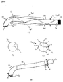
図5、6は第2の実施形態を説明するための図である。第1の実施形態と同じ個所、または、同じ機能を有する箇所に関しては説明を省略する。また、図中で同じ符号の箇所は、同様の機能を有する箇所である。図5(a)は、側面から電子顕微鏡を見た図で、図5(b)は、図5(a)の矢印Aの方向から電子顕微鏡1を見た図である。点線Bと出射面の中心を含む平面を平面S1とした場合に、図6(a)は、平面S1におけるライトガイド3の断面図である。また、平面S1は入射面3aの中心も含む面である。
図5、6は第2の実施形態を説明するための図である。第1の実施形態と同じ個所、または、同じ機能を有する箇所に関しては説明を省略する。また、図中で同じ符号の箇所は、同様の機能を有する箇所である。図5(a)は、側面から電子顕微鏡を見た図で、図5(b)は、図5(a)の矢印Aの方向から電子顕微鏡1を見た図である。点線Bと出射面の中心を含む平面を平面S1とした場合に、図6(a)は、平面S1におけるライトガイド3の断面図である。また、平面S1は入射面3aの中心も含む面である。
図5に例示するような電子顕微鏡には、図1で例示したような信号粒子制限板がなく、二次粒子101は直接シンチレータ5に入射する。また、図1の例と比較すると、ライトガイド形状が異なる。本実施形態のライトガイド3は、入射面3aと出射面3bが対向していない(シンチレータの入射面の法線方向に、シンチレータの出射面がない)ため、ライトガイド3には屈曲部3fが設けられている。
なお、簡単のため、検出系は1つのみ示しているが、複数の検出系を設けても良いし、信号粒子制限板がある別の検出系を設けてもよい。本実施形態では図示していないが、信号粒子制限板がある別の検出系が、図示されている検出系より試料50に近い側に設けられている。
本実施形態の電子光学系は、電子源2から放出された一次電子線100は試料50に向かって直進するが、二次粒子101はシンチレータ5に向かって曲がることができる光学系を有する。二次粒子101が直接シンチレータ5に入射するので、試料50から直進してきた二次粒子101を高感度に検出することが可能である。
図5(b)で示すようにライトガイド3は屈曲部3fを有し、光も屈曲部3fを反射しながら出射面3bに向かって導光し、受光素子4に到達する。図6(a)を用いて断面形状を詳細に説明する。断面形状は大きく、3つの部位からなる。屈曲部3f1、3f2と、屈曲部よりなだらかに形状が変化する傾斜部3g1、3g2と、直線部3h1、3h2の3つの部位である。
直線部3hの形状は出射面3bを底面(半径raの円、図6(b)参照)とする円柱である。直線部3hには、分離フランジ3cが設けられている。直線部3hに分離フランジ3cを設けることで、電子光学鏡筒60の側壁などに垂直に分離フランジ3cを押し当てることができ、大気が真空に流入することを抑制する構成となっている。
傾斜部3gの形状は、屈曲部3fと直線部3hを接続する形状である。断面形状3g1、3g2は緩やかに変化する曲線である。断面形状は曲線に限らず、直線、折れ線、曲線と直線、曲線と折れ線の組み合わせなどでも良い。
屈曲部の断面形状3f1、3f2は、本実施形態では、中心角が60度から89度の間にある円弧である。なお、当該断面形状は、円弧からずれた曲線などでも良いし、一部は円弧または曲線で、その他は直線または折れ線でも良い。屈曲部は屈曲部の表面からライトガイドの外に漏れる光の量を低減するために複雑な形状をしている。入射面3aは、図6(c)に示す形状で、点DおよびEに断面形状3f1および3f2がそれぞれ接続する。点線Fを境に左半分が円3a1、右半分が楕円3a2となっている。円の半径はraで、楕円の短軸、長軸の1/2の長さは、それぞれraとrbである(ra<rb)。点線Fと、点DとEが結ぶ線分との交点に略対向する位置にシンチレータ5の中心が配置される。
平面S1に垂直で点線Cを含む面を平面S2とした場合に、平面S2におけるライトガイド3の断面形状は出射面3bと同じ円である。屈曲部3fの形状は、当該円と入射面3aの形状を、断面形状3f1、3f2を輪郭として繋いだ形状である。例えば、一般的な3D CAD(three-dimensional computer aided design system)を用いて、当該円と入射面3aの形状を、断面形状3f1、3f2を輪郭としてロフトすることで屈曲部の形状が作成できる。図6(d)は本実施形態のライトガイド3の斜視図である。符号3iは、ライトガイド3とシンチレータ5を固定するための部位を示す。
図7を用いて、屈曲部の形状をより詳細に説明する。図7(a)は屈曲部3fで光が漏れる要因を説明するための平面S1における断面図である。この例では、図6で示したライトガイドのように傾斜部3gが存在しない。入射面3aと出射面3bの形状は図6(b)に示す円で、屈曲部の断面形状3f1、3f2は中心角90度、入射面3aを始点する円弧である。屈曲部3fと出射面3bは直線部3hで繋がれている。入射面3aと出射面3bを繋げる最も簡単なライトガイド形状である。
3本の光線例を用いて代表的な光が漏れる光線経路を説明する。光線RayF5は、屈曲部の断面3f1に到達し、到達点の面の法線3N1との角度が全反射の臨界角よりも小さいために、面を透過する例である。入射面3aの法線と入射面3aを出射するときの光線の角度が、図の角度より大きい光線は全て屈曲部3fを透過して損失となる。
光線RayF6(他の光線と見分けるために点線で示す。)は、屈曲部の断面3f2で、入射面3aの法線方向に全反射して、屈曲部の断面3f1に到達し、到達点の面の法線3N2との角度が全反射の臨界角よりも小さいために、面を透過する例である。屈曲部の断面3f2に近い位置から出射する光は、屈曲部の断面3f2で反射して同様の光線経路でライトガイド3から漏れる。
光線RayF7は、入射面3aの法線から出射面3bの方へ傾いて、入射面3aから出射した光線が、直線部の断面3h1に到達して、到達点の面の法線3N3との角度が全反射の臨界角よりも小さいために、面を透過する例である。入射面3aの法線と略平行な法線を持つ面に到達した光は、当該面を透過する確率が高い。透過率はフレネルの透過率に従う。
図6(a)に示したライトガイド3は、これら光漏れを抑制する形状となっている。図7(b)に示すライトガイドは、図6(a)に示したライトガイド3であり、当該図を用いて、光漏れ抑制効果を説明する。図7(b)のライトガイド3の主な特徴は、図7(a)に比べて屈曲部の断面3f1の曲率半径が大きい点と、入射面3aの形状が図6(c)に示した長軸が出射面の方向にある楕円を含む形状である点である。屈曲部の断面3f1の曲率半径が大きいがゆえに、入射面3aと出射面3bとの間の領域以外にも、光を出射面3bに案内するライトガイド3の表面が存在する構成である。入射面3aと出射面3bとの間の領域とは、図7(b)において、矢印DAで示される領域である。矢印が指す点線は領域を示すための補助線で、図中下側の点線は入射面3aの端部と一致し、上側の点線は出射面3bの端部と一致する。図7(a)に示す傾斜部のないライトガイドは、当該領域以外には、光を出射面3bに案内するライトガイド3の表面が存在しない。なお、分離フランジ3cなどの固定部位は、光を出射面3bに案内する表面ではない。
屈曲部の断面3f1の曲率半径が大きいと、屈曲部で全反射が起きやすくなる。光線RayF8は、光線RayF5と同じ角度で入射面3aから出射する光線であるが、屈曲部の断面3f1への入射角度は、光線RayF5の場合よりも大きく、全反射する。曲率半径が大きいので、円弧へ光が入射する位置の法線3N4が入射面3aの法線から大きく傾いた位置に入射する。それゆえ、屈曲部で全反射する光の量が増え、ライトガイドの光利用効率が向上する。
光線RayF10は、光線RayF7と同じ角度で入射面3aから出射する光線である。曲率半径が大きいので、光線RayF10は終点付近の屈曲部の断面3f1に入射し、全反射して導光する。終点付近の屈曲部の断面3f1の法線3N6は、入射面3aから出射面3bとは反対方向に傾いているので、法線3N6と入射光線との角度は大きくなり、全反射し易くなる。全反射しない場合でもフレネル反射率は向上するので、反射する光の量が増え、ライトガイドの光利用効率が向上する。
シンチレータ5が直径9mmの円柱の場合に、入射面3aを直径10mmの円とし、屈曲部の断面3f1および3f2の曲率半径を、それぞれ15mm、5mmから18mm、8mmに変更することで、光利用効率が37%向上することを光線追跡計算により確認した。
光線RayF9は、光線RayF6と同じ角度で入射面3aから出射する光線である。入射面3aの一部を長軸が出射面の方向にある楕円とし、屈曲部の断面3f2を出射面3b側に移動することで、光線RayF9は、断面3f2で反射すること無く傾斜部の断面3g1に到達することが可能となる。光線RayF9は、断面3g1で必ずしも全反射はしないが、光線RayF6の場合に比べて、断面3g1の入射点において、光線RayF9と法線3N5との角度が大きくなるので、フレネル反射率は大きくなり、導光する光の量が増え、光利用効率が向上する。
ここで、入射面3aの楕円部の形状に関して説明する。例えば、シンチレータ5の半径が4.5mmの場合、図6(c)において、raとrbは、それぞれ4.5mm、5.5mmとすると、入射面3aを直径9mmの円とした場合に比較して、光利用効率が数%向上することを光線追跡計算により確認した。本実施形態では、入射面3aの一部を楕円とし、形状を出射面側に長くすることで断面3f2を出射面側に移動して光利用効率を向上させたが、入射面3aの一部を楕円とすることには限定されず、形状を出射面側に長くすれば良い。別の言い方をすれば、シンチレータ5の中心から入射面3aの端部までの距離が、出射面方向とそれとは反対方向で異なり、出射面方向の距離が長ければ良い。
次に、屈曲部3fの一部または全部を円弧とする場合の形状に関して、図7(c)、(d)を用いて説明する。屈曲部の断面形状3f1は本実施形態の円弧の形状である。断面形状3f1C(点線で示す)は、円弧の中心CP1が入射面3aを含む平面SP(点線で示す)内に存在し、断面形状3f1Cの入射面3aから立ち上がる接線が入射面の法線3aNと平行の場合の断面形状である。断面形状3f1Cは、図7(a)に示す傾斜部のないライトガイドを構成する場合の屈曲部の形状であり、屈曲部として最も簡単な形状と言える。
断面形状3f1は、円弧の中心CP2が平面SP内には存在しない構成であり、入射面3aより下側(ライトガイド3から離れる方向)にある。さらに、断面形状3f1の入射面3aから立ち上がる接線3f1Tと入射面の法線3aNは所定の角度θtを持つ形状である。角度θtは2度から10度程度の範囲であることが光利用効率向上の観点で望ましい。図7(b)に示したライトガイド3の角度θtは2.5度である。また、中心CP2と平面SPの距離は1mmである。当該距離は0.3mmから5mm程度の範囲内にあることが望ましい。
ライトガイド3の表面をあるラインで分割し、外側曲面と内側曲面とした場合に、断面形状3f1は、入射面3aの端部を始点とした外側曲面に含まれ、断面形状3f2は内側曲面に含まれる。上述した構成は、当該外側曲面と入射面3aとの接点において、入射面の法線3aNより、当該外側曲面は前記入射面側に傾いた接線を有する構成である。
光線RayF11は入射面の法線3aNと平行方向に入射面3aの略中心から屈曲部へ出射する光線である。なお、シンチレータ5から発光する光強度は、一般に当該方向および位置の強度が最も大きい。符号3f1N、3f1CNは、それぞれ断面3f1および3f1Cと光線RayF11の交点における法線を示す。角度θ1、θ2は、法線3f1Nと光線RayF11および3f1CNと光線RayF11がそれぞれ成す角度である。図7(d)は、角度θ1、θ2を比較するための図であり、光線RayF11と各断面の交点を一致させた図である。この図から分かるように角度θ1の方が角度θ2よりも大きくなる。したがって、断面3f1の方が光線RayF11の当該断面への入射角度が大きくなるので、ライトガイド3に入射する光束のうち全反射する光束の割合が増え、さらに、フレネル反射率が大きくなるので、光漏れが低減され光利用効率が向上する。
つまり、断面形状3f1の一部(望ましくは、RayF11が入射する部位)が円弧であって、円弧の中心CP2が入射面3aを含む平面SP内には存在しない構成である場合に光利用効率は向上する。また、断面形状3f1の入射面3aから立ち上がる接線3f1Tと入射面の法線3aNが所定の角度θtを持つ形状である場合に光利用効率は向上する。
傾斜部の断面形状3g1と断面形状3g2は、本実施形態のように略平行とすることが望ましい。なぜならば、図7(b)に示すように、出射面3bに向けてライトガイドの高さが小さくなる場合、断面形状3g1への入射角度は、断面形状3g1へ光が入射する度に小さくなるが、断面形状3g2への入射角度は、断面形状3g2へ光が入射する度に大きくなるので(ライトガイドの高さが大きくなる場合、現象が逆になる。)、入射角度が補償される。それゆえ、最初に傾斜部3gに入射したときの入射角度が導光途中で大きくは変化せず、全反射角度より入射角度が小さくなり光漏れが起こるのを抑制するという効果を奏する。
本実施形態では、屈曲部の断面形状3f1、3f2を円弧としたが、これに限定されず、円の方程式からずれた曲線でも折れ線でも良い。但し、屈曲部の外側の断面形状3f1は、円、楕円、放物線の方程式を用いて部分的にはフィッティングされる形状であることが望ましい。
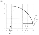
図8のグラフを用いて、屈曲部の断面形状3f1を円の方程式を用いてフィッティングした例を説明する。参考のためグラフ中に入射面3aの位置を記入した。本グラフにおいて、断面形状3f1は、図6、図7に記載のライトガイドの断面形状とは、反対向きで記載されている。横軸は入射面に平行な位置座標[mm]を表し、縦軸は入射面の法線に平行な方向の位置座標[mm]を示す。点線は屈曲部の断面形状3f1の一例であり、完全な円弧とはなっていない。実線3f1Fは点線を円の方程式でフィッティングした結果である。点線と実線は、入射面3aの端部付近を除いて良く一致している。このフィッティング結果を用いて円弧の中心P1等を求めれば良い。
本実施形態では、入射面3aおよび出射面3bの形状として、円、一部円と楕円等を用いたが、本発明はこれに限定されない。たとえば、シンチレータ5が四角形の角柱であれば、入射面を四角としても良く、受光素子の形状が四角であれば出射面を四角にしても良く、さまざまな形状が考えられる。また、例えば出射面と平行な面の断面形状は、円などに限定されるものではなく、四角や六角など様々な形状が考えられる。
《第3の実施形態》
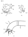
図9は第3の実施形態を説明するための図である。第1の実施形態と同じ個所、または、同じ機能を有する箇所に関しては説明を省略する。また、図中で同じ符号の箇所は、同様の機能を有する箇所である。第1の実施形態と異なる箇所は、屈曲部3fを有するライトガイド3に側面プリズム3eを設けた点である。図9は、屈曲部3fと側面プリズム3eに着目した断面図である。なお、本実施形態のライトガイド3の形状は、側面プリズム3eが付与されている部位以外は、第2の実施形態で図6(b)を用いて説明したライトガイドと同じである。
図9は第3の実施形態を説明するための図である。第1の実施形態と同じ個所、または、同じ機能を有する箇所に関しては説明を省略する。また、図中で同じ符号の箇所は、同様の機能を有する箇所である。第1の実施形態と異なる箇所は、屈曲部3fを有するライトガイド3に側面プリズム3eを設けた点である。図9は、屈曲部3fと側面プリズム3eに着目した断面図である。なお、本実施形態のライトガイド3の形状は、側面プリズム3eが付与されている部位以外は、第2の実施形態で図6(b)を用いて説明したライトガイドと同じである。
図9(a)は、入射面3aのシンチレータ5が対向していない部位に側面プリズム3eを設置した例である。当該部位は入射面3aの楕円の長軸方向先端部で、もともと光はほとんど入射しない位置であり、かつ、入射面3a以降のライトガイド形状に影響を与えないので、導光にも影響を与えない。したがって、当該位置に側面プリズム3eを設置する場合、入射面3a以降のライトガイド形状と側面プリズム3eを独立に最適化することが可能となる。
側面プリズム3eを設置することで光利用効率を向上するという効果を奏する。なお、側面プリズム3eの変形は、第1の実施形態において図4を用いて説明したように様々な変形が可能である。特に、反射面3e2の表面に反射部材を付与することで効果的に光利用効率を向上することが可能となる。符号RayS7は光線例である。
図9(b)は、外側の屈曲部3f1にも側面プリズム3eoを設置した例で、外側の側面プリズム3eoは光の伝播方向を略180度回転して出射面側に反射する必要があるので、反射面を2つ以上有する構成となる。つまり、側面プリズム3eoは、光を2回以上反射する反射面形状を有する。図9(b)は、シンチレータ5の側面5dに対向し、側面5dからの光を入射する側面プリズム入射面3eo1を有し、反射面3eo2で略入射面3aの法線方向に光を反射し、反射面3eo3で略出射面3bの方向に光を反射している例である。このような構成とすることで、光利用効率を向上するという効果を奏する。但し、外側の側面プリズム3eoの場合は、断面形状3f1に変更を加えるので、導光に影響を与える。それゆえ、側面プリズム 3eoの影響で大きな光漏れが発生し、全体としての光利用効率が低下しないように形状を小さくすることが好ましい。また、例えば、反射面3eo3を、断面形状3f1の一部として、点線で示す断面形状3f1’のように、入射面3aと略同位置まで連続的な形状とすることが好ましい。符号RayS8は光線例である。
図9(b)の変形例を、図10を用いて説明する。図10(a)は屈曲部3fと側面プリズム3eに着目した断面図である。本変形例と図9(b)の形状で異なる点は、外側の側面プリズム3eoと屈曲部3f間に空隙を設けた構成である。前述したように、断面形状3f1に変更を加えると導光に影響を与えるので、影響を与えないように空隙を設けている。入射面3aから入射した光は、断面形状3f1と3f2で反射して導光し、側面プリズム入射面3e1、3eo1から入射した光は、側面プリズム3e、3eoで反射して導光する構成である。
図10(b)は、側面プリズム3eoをより詳細に説明する断面図である。光はシンチレータと対向する面3eo1から入射し、反射面3eo2、3で反射して、屈曲部3fと対向する側面プリズム出射面3eo4から出射して、屈曲部3fに入射する。反射面3eo2、3eo3としては、第1の実施形態において図4を用いて説明したように様々な変形が可能である。例えば、反射面3eo2と反射面3eo3を連続的な曲面としても良い。その際には、当該曲面に、略入射面3aの法線方向に光を反射し、その後で略出射面3bの方向に光を反射する機能があれば良い。また、反射面3eo2、3eo3にアルミニウムなどの反射部材を付与すると、効果的に光利用効率を向上できる。
なお、側面プリズム出射面3eo4と屈曲部3f間を全て空隙として示しているが、一部は結合していても良い。例えば、側面プリズム出射面3eo4の入射面3aに近い位置は屈曲部3fと結合していても良い。なぜならば、結合部が小さければ入射面3aから入射した光の導光への影響は小さいためである。
外側の側面プリズム3eoとライトガイド3は一体としても良いが、空隙を設けるため、別体として、側面プリズム3eoをライトガイド3に取り付けても良い。
図10(c)は、入射面3aが見える方向からの斜視図である。図中矢印aの方向(入射面3aの法線方向)からライトガイド3を見た図が図11(a)である。図中矢印bの方向から見た図が図11(b)で、図中矢印cの方向から見た図が図11(c)である。図11(a)を見ると、シンチレータ5(点線で図示)に沿って側面プリズム3e、3eoが配置されていることが分かる。入射面3aと外側の側面プリズム3eoとの間に空隙AIRがある。
本変形例の構成とすることで、側面プリズム3eoを備えることによる入射面3aからの入射光の導光への影響をなくしつつ、光利用効率を向上させるという効果を奏する。
次に別の変形例に関して平面S1における断面を示す図12を用いて説明する。本変形例は、屈曲部3fの断面形状において曲線が1つの場合である。入射面3aから入射した光の一部は、光線例RayF12のように断面形状3f1で反射して直線部3hに入射して導光する。側面プリズム入射面3eo1から入射した光の一部は、光線例RayS9のように、反射面3eo2で反射して、屈曲部3fの曲面と連続的に繋がっている反射面3eo3で反射して、出射面3bに向かって導光する。側壁面3e1’から入射した光は、光線例RayS10のように出射面3bに向かって導光する。本変形例は、入射面3aに対向した曲面と、入射面3a、側面プリズム入射面3eo1と側壁面3e1’に囲まれた収容空間と、側面プリズム3eo1を設けることで、シンチレータ5から出射する全方位の光をライトガイド3に取り込み、導光させることが可能となり、光利用効率を向上するという効果を奏する。なお、本変形例の収容空間は、シンチレータ5の光を出射する全ての面に対向して、光が入射する面を有しているが、シンチレータ5の光を出射する面の一部に対向して、光が入射する面を有することでも光利用効率を向上するという効果を奏する。
次に別の変形例に関して平面S1における断面を示す図13を用いて説明する。本変形例は、ある断面において、受光素子4が左右両側に配置され、両側に光を伝播させるために、ライトガイド3がシンチレータ5に対向する位置で二股に分かれる形状である。本変形例では、シンチレータ5の中心を通る中心線CL1に対して断面3f1は左右対称な形状である。左右対称とすることで、入射面3aから入射した光の伝搬方向を回転する角度を小さく(略90度内と)することが可能となる。一般に、光の伝播方向を回転する角度が大きくなるほど、受光素子4に届くように光を反射させることが難しくなり、ライトガイド3から漏れる光が多くなる。それゆえ、屈曲部の断面3f1を中心線CL1に対して、左右対称とすることで、光利用効率が向上するという効果を奏する。シンチレータ5の両側の側面5dに対向して、側面プリズム入射面3e1が配置される構成である。左右それぞれの受光素子4に入射する光線例を、RayS11、RayS12として記載した。何れも、側面プリズム入射面3e1から入射し、反射面3e2で反射した後で、断面形状3f2、3f1で順次反射して、直線部3h2で反射して、出射面3bから受光素子4に入射する例である。受光素子4が左右両側に配置される構成であっても、側面プリズムを有する構成により、光利用効率を向上させることが可能となる。本構成は、側面プリズム3eにより、180度伝播方向を回転させられる光線が無い、もしくは、ほとんど無い。したがって、光の伝搬方向を回転する角度が小さいので、光利用効率が向上するという効果を奏する。また、図9(b)において示した外側の屈曲部3f1に設置される側面プリズム3eoが無いので、外側の屈曲部3f1と側面プリズム3eを別々に最適化でき、光利用効率が向上するという効果を奏する。図13には直線部の断面3h1と屈曲部の断面3f1の間に傾斜部が存在しないが、屈曲部の断面3f1の曲率半径を大きくして光利用効率を高め、傾斜部を有する構成としても良い。
以上より、本構成のように、ある断面で見た場合に両側に受光素子4を設ける構成は、光利用効率が向上するという効果を奏する。また、反射面3e2は、第1から第3の実施形態3で説明した様々な形状を取ることができる。なお、シンチレータ5をドーナツ状の形状として、中心線CL1に沿って、1次電子線100など、粒子を貫通させる場合に、ライトガイド5も中心線CL1に沿って貫通穴を設けても良い。当該貫通穴は、円、四角など様々な形状が考えられる。以上、第1の実施形態から第3の実施形態まで説明したが、それぞれで記載した事項は適宜組み合わせても良く、組み合わせることでより大きな効果を奏することもある。
上記構成によれば、光利用効率を向上させることが可能となる。
1 電子顕微鏡
2 電子源
3 ライトガイド
4 受光素子
5 シンチレータ
6 信号粒子制限板
50 試料
60 電子光学鏡筒
61 試料室
100 一次電子線
101 二次粒子
2 電子源
3 ライトガイド
4 受光素子
5 シンチレータ
6 信号粒子制限板
50 試料
60 電子光学鏡筒
61 試料室
100 一次電子線
101 二次粒子
Claims (14)
- シンチレータより発生した光を受光素子に導くライトガイドにおいて、
前記シンチレータの荷電粒子入射面とは反対の面に対向する第1の面と、前記シンチレータの荷電粒子入射面の反対の面とは異なる面に対向する第2の面から形成されるシンチレータ収容部と、前記第2の面から入射する光を、前記ライトガイド内部に向かって反射する傾斜面を備えたことを特徴とするライトガイド。 - 請求項1において、
前記第1の面は、前記第2の面より大きいことを特徴とするライトガイド。 - 請求項1において、
前記傾斜面には、反射部材が設けられていることを特徴とするライトガイド。 - 請求項1において、
前記傾斜面は、複数の異なる方向に向いた面、或いは曲面で形成されることを特徴とするライトガイド。 - 請求項1において、
前記シンチレータは、前記第1の面、及び第2の面から入射した光を異なる方向に案内する屈曲部を備えていることを特徴とするライトガイド。 - 請求項5において、
前記受光素子に対向した位置に形成される出射面と、当該出射面に前記光を案内する直線部と、当該直線部と、前記屈曲部との間に形成される傾斜部とを備えたことを特徴とするライトガイド。 - 請求項5において、
前記屈曲部の外側に位置する前記傾斜面は、前記屈曲部の内側に位置する前記傾斜面に対し、相対的に入射光と出射光の相対角が狭くなるように形成されていることを特徴とするライトガイド。 - シンチレータと、当該シンチレータより発生した光を受光素子に導くライトガイドを備えた検出器において、
前記ライトガイドは、前記シンチレータの荷電粒子入射面とは反対の面に対向する第1の面と、前記シンチレータの荷電粒子入射面の反対の面とは異なる面に対向する第2の面から形成される凹部と、前記第2の面から入射する光を前記ライトガイド内部に向かって反射する傾斜面とを備え、当該凹部に前記シンチレータが収容されることを特徴とする検出器。 - 荷電粒子源から放出される荷電粒子ビームの照射に基づいて試料から放出される荷電粒子、及び試料から放出される荷電粒子が他部材に衝突することによって発生する荷電粒子の少なくとも一方を検出する検出器を備えた荷電粒子線装置において、
前記検出器はシンチレータと、当該シンチレータより発生した光を受光素子に導くライトガイドを有し、当該ライトガイドは、前記シンチレータの荷電粒子入射面とは反対の面に対向する第1の面と、前記シンチレータの荷電粒子入射面の反対の面とは異なる面に対向する第2の面から形成される凹部と、前記第2の面から入射する光を前記ライトガイド内部に向かって反射する傾斜面とを備え、当該凹部に前記シンチレータが収容されていることを特徴とする荷電粒子線装置。 - 光の入射面と、当該入射面から入射した光を出射する出射面と、前記入射面から入射した光を前記出射面に案内する表面を備えたライトガイドを備えた荷電粒子線装置であって、
前記表面は、前記入射面端を始点とした外側曲面を有し、
当該外側曲面と前記入射面との接点において、前記入射面の法線より、当該外側曲面は前記入射面側に傾いた接線を有するライトガイドを備えたことを特徴とする荷電粒子線装置。 - 請求項10において、
前記入射面と当該入射面とは異なる方向に面方向を有する側壁面からなるシンチレータ収容空間と、前記側壁面から入射した光を反射する反射面が形成されていることを特徴とする荷電粒子線装置。 - 請求項11において、
前記反射面は、光を2回以上反射する形状であることを特徴とするライトガイドを備えた荷電粒子線装置。 - 請求項10において、
前記入射面と出射面との間のライトガイドの一部に曲面を有することを特徴とする荷電粒子線装置。 - 請求項10において、
前記外側曲面は、円の方程式で近似できる部位を有し、当該円の中心は前記入射面と平行な面内にないことを特徴とする荷電粒子線装置。
Priority Applications (3)
| Application Number | Priority Date | Filing Date | Title |
|---|---|---|---|
| DE112017001072.1T DE112017001072B4 (de) | 2016-03-31 | 2017-02-03 | Lichtleiter, Detektor mit Lichtleiter und Ladungsträgerstrahlvorrichtung |
| US16/082,745 US10593512B2 (en) | 2016-03-31 | 2017-02-03 | Light guide, detector having light guide, and charged particle beam device |
| US16/751,705 US10679821B1 (en) | 2016-03-31 | 2020-01-24 | Light guide, detector having light guide, and charged particle beam device |
Applications Claiming Priority (2)
| Application Number | Priority Date | Filing Date | Title |
|---|---|---|---|
| JP2016-069943 | 2016-03-31 | ||
| JP2016069943A JP6739207B2 (ja) | 2016-03-31 | 2016-03-31 | 荷電粒子線装置 |
Related Child Applications (2)
| Application Number | Title | Priority Date | Filing Date |
|---|---|---|---|
| US16/082,745 A-371-Of-International US10593512B2 (en) | 2016-03-31 | 2017-02-03 | Light guide, detector having light guide, and charged particle beam device |
| US16/751,705 Continuation US10679821B1 (en) | 2016-03-31 | 2020-01-24 | Light guide, detector having light guide, and charged particle beam device |
Publications (1)
| Publication Number | Publication Date |
|---|---|
| WO2017169101A1 true WO2017169101A1 (ja) | 2017-10-05 |
Family
ID=59963950
Family Applications (1)
| Application Number | Title | Priority Date | Filing Date |
|---|---|---|---|
| PCT/JP2017/003884 Ceased WO2017169101A1 (ja) | 2016-03-31 | 2017-02-03 | ライトガイド、ライトガイドを備えた検出器、及び荷電粒子線装置 |
Country Status (4)
| Country | Link |
|---|---|
| US (2) | US10593512B2 (ja) |
| JP (1) | JP6739207B2 (ja) |
| DE (1) | DE112017001072B4 (ja) |
| WO (1) | WO2017169101A1 (ja) |
Cited By (1)
| Publication number | Priority date | Publication date | Assignee | Title |
|---|---|---|---|---|
| WO2026053275A1 (ja) * | 2024-09-03 | 2026-03-12 | 株式会社日立ハイテク | 検出器及び測定装置 |
Families Citing this family (5)
| Publication number | Priority date | Publication date | Assignee | Title |
|---|---|---|---|---|
| JP6739207B2 (ja) * | 2016-03-31 | 2020-08-12 | 株式会社日立ハイテク | 荷電粒子線装置 |
| JP6984035B2 (ja) | 2018-09-21 | 2021-12-17 | 株式会社日立ハイテク | 荷電粒子線装置 |
| JP7140902B2 (ja) * | 2018-09-21 | 2022-09-21 | 株式会社日立ハイテク | 荷電粒子線装置 |
| US11239048B2 (en) * | 2020-03-09 | 2022-02-01 | Kla Corporation | Arrayed column detector |
| JP7076021B1 (ja) | 2021-03-10 | 2022-05-26 | 浜松ホトニクス株式会社 | ライトガイド、電子線検出器、及び荷電粒子装置 |
Citations (1)
| Publication number | Priority date | Publication date | Assignee | Title |
|---|---|---|---|---|
| US20130234032A1 (en) * | 2012-03-12 | 2013-09-12 | Hermes-Microvision, Inc. | High efficiency secondary and back scattered electron detector |
Family Cites Families (21)
| Publication number | Priority date | Publication date | Assignee | Title |
|---|---|---|---|---|
| JPS5470359U (ja) * | 1977-10-26 | 1979-05-18 | ||
| WO2001041180A1 (de) * | 1999-11-29 | 2001-06-07 | Leo Elektronenmikroskopie Gmbh | Detektor für ein rasterelektronenmikroskop mit variablem druck und rasterelektronenmikroskop mit einem solchen detektor |
| CZ302126B6 (cs) * | 2000-07-07 | 2010-11-03 | Leo Elektronenmikroskopie Gmbh | Detektor pro prístroje vyzarující korpuskulární zárení, prístroj vyzarující korpuskulární zárení a zpusob detekování existence produktu vzájemného pusobení v tomto prístroji |
| GB2367686B (en) * | 2000-08-10 | 2002-12-11 | Leo Electron Microscopy Ltd | Improvements in or relating to particle detectors |
| JP4636897B2 (ja) * | 2005-02-18 | 2011-02-23 | 株式会社日立ハイテクサイエンスシステムズ | 走査電子顕微鏡 |
| US7745786B2 (en) * | 2008-03-19 | 2010-06-29 | Fama Leo A | Method and apparatus allowing simultaneous direct observation and electronic capture of scintillation images in an electron microscope |
| JP5352262B2 (ja) * | 2009-02-06 | 2013-11-27 | 株式会社日立ハイテクノロジーズ | 荷電粒子線装置 |
| JP5529573B2 (ja) | 2009-02-10 | 2014-06-25 | 国立大学法人 東京大学 | 透過型電子顕微鏡 |
| JP5372570B2 (ja) * | 2009-03-30 | 2013-12-18 | 株式会社日立ハイテクノロジーズ | ナノポアを用いたバイオポリマー決定方法、システム、及びキット |
| US8829451B2 (en) * | 2012-06-13 | 2014-09-09 | Hermes Microvision, Inc. | High efficiency scintillator detector for charged particle detection |
| JP5967538B2 (ja) | 2012-09-25 | 2016-08-10 | 株式会社日立ハイテクノロジーズ | 電子顕微鏡および電子線検出器 |
| JP2014067256A (ja) | 2012-09-26 | 2014-04-17 | Canon Inc | 交流負荷電力制御方式 |
| JP5865403B2 (ja) * | 2014-02-12 | 2016-02-17 | 株式会社日立ハイテクノロジーズ | 流路切り替えバルブおよび当該バルブを用いた液体クロマトグフラフ装置 |
| JP6169506B2 (ja) * | 2014-02-19 | 2017-07-26 | 株式会社日立ハイテクノロジーズ | 試料ホルダ、観察システム、および画像生成方法 |
| US9778186B2 (en) | 2014-04-15 | 2017-10-03 | Kla-Tencor Corporation | System for electron beam detection |
| US9431211B2 (en) * | 2014-08-22 | 2016-08-30 | The United States Of America, As Represented By The Secretary Of Commerce | Hybrid electron microscope |
| EP3139399B1 (en) * | 2015-09-03 | 2019-05-29 | El-Mul Technologies Ltd | Electron detector assembly |
| US9759883B1 (en) * | 2016-03-14 | 2017-09-12 | Applied Materials Israel Ltd. | Optical module and a detection method |
| JP6739207B2 (ja) * | 2016-03-31 | 2020-08-12 | 株式会社日立ハイテク | 荷電粒子線装置 |
| JP2018170166A (ja) * | 2017-03-30 | 2018-11-01 | 株式会社日立ハイテクノロジーズ | 荷電粒子線装置 |
| JP6850234B2 (ja) * | 2017-09-29 | 2021-03-31 | 株式会社日立ハイテク | 荷電粒子線装置 |
-
2016
- 2016-03-31 JP JP2016069943A patent/JP6739207B2/ja active Active
-
2017
- 2017-02-03 WO PCT/JP2017/003884 patent/WO2017169101A1/ja not_active Ceased
- 2017-02-03 DE DE112017001072.1T patent/DE112017001072B4/de active Active
- 2017-02-03 US US16/082,745 patent/US10593512B2/en active Active
-
2020
- 2020-01-24 US US16/751,705 patent/US10679821B1/en active Active
Patent Citations (1)
| Publication number | Priority date | Publication date | Assignee | Title |
|---|---|---|---|---|
| US20130234032A1 (en) * | 2012-03-12 | 2013-09-12 | Hermes-Microvision, Inc. | High efficiency secondary and back scattered electron detector |
Cited By (1)
| Publication number | Priority date | Publication date | Assignee | Title |
|---|---|---|---|---|
| WO2026053275A1 (ja) * | 2024-09-03 | 2026-03-12 | 株式会社日立ハイテク | 検出器及び測定装置 |
Also Published As
| Publication number | Publication date |
|---|---|
| US20200203120A1 (en) | 2020-06-25 |
| DE112017001072B4 (de) | 2022-03-17 |
| US20190115186A1 (en) | 2019-04-18 |
| US10679821B1 (en) | 2020-06-09 |
| JP6739207B2 (ja) | 2020-08-12 |
| US10593512B2 (en) | 2020-03-17 |
| JP2017183126A (ja) | 2017-10-05 |
| DE112017001072T5 (de) | 2018-12-20 |
Similar Documents
| Publication | Publication Date | Title |
|---|---|---|
| US10679821B1 (en) | Light guide, detector having light guide, and charged particle beam device | |
| JP5294557B2 (ja) | 発光ダイオード用偏向レンズ | |
| US20120162644A1 (en) | Microparticle detection apparatus | |
| US11694873B2 (en) | Charged particle beam apparatus | |
| US20130334430A1 (en) | High efficiency scintillator detector for charged particle detection | |
| TW201338003A (zh) | 高效能二次電子與反向散射電子探測器 | |
| US20180266638A1 (en) | Light source device, lighting apparatus, and vehicle lamp device | |
| KR20190079559A (ko) | 미러 기반 광 이미징 대전 입자 현미경에서의 se 검출 향상을 위한 방법 및 장치 | |
| JP6919014B2 (ja) | 荷電粒子線装置 | |
| TW201527148A (zh) | 車輛頭燈裝置 | |
| CN202814877U (zh) | 荧光收集装置 | |
| US20060219959A1 (en) | Radiation source for the generation of short-wavelength radiation | |
| US9036789B2 (en) | X-ray apparatus and its adjusting method | |
| JP2017183126A5 (ja) | 荷電粒子線装置 | |
| US20150260970A1 (en) | Annular optical device | |
| US8579474B2 (en) | Bézier curve reflector, light source arrangement and projector apparatus | |
| JP7140902B2 (ja) | 荷電粒子線装置 | |
| CN117054384A (zh) | 荧光探测系统 | |
| US20140098518A1 (en) | Device for the beam shaping of light | |
| CN222732684U (zh) | 一种新型小角度透镜结构 | |
| CN117289241B (zh) | 一种激光扫描系统 | |
| TW202236346A (zh) | 光導,電子線檢測器,及帶電粒子裝置 | |
| TW200933085A (en) | Illumination system | |
| CN120530474A (zh) | 检测器、测量装置以及带电粒子束装置 | |
| WO2010007811A1 (ja) | 光学ユニット |
Legal Events
| Date | Code | Title | Description |
|---|---|---|---|
| 121 | Ep: the epo has been informed by wipo that ep was designated in this application |
Ref document number: 17773650 Country of ref document: EP Kind code of ref document: A1 |
|
| 122 | Ep: pct application non-entry in european phase |
Ref document number: 17773650 Country of ref document: EP Kind code of ref document: A1 |