WO2017164309A1 - 光学体及び発光装置 - Google Patents
光学体及び発光装置 Download PDFInfo
- Publication number
- WO2017164309A1 WO2017164309A1 PCT/JP2017/011729 JP2017011729W WO2017164309A1 WO 2017164309 A1 WO2017164309 A1 WO 2017164309A1 JP 2017011729 W JP2017011729 W JP 2017011729W WO 2017164309 A1 WO2017164309 A1 WO 2017164309A1
- Authority
- WO
- WIPO (PCT)
- Prior art keywords
- uneven structure
- micro
- macro
- optical body
- light
- Prior art date
Links
Images


Classifications
-
- G—PHYSICS
- G02—OPTICS
- G02B—OPTICAL ELEMENTS, SYSTEMS OR APPARATUS
- G02B5/00—Optical elements other than lenses
- G02B5/04—Prisms
- G02B5/045—Prism arrays
-
- G—PHYSICS
- G02—OPTICS
- G02B—OPTICAL ELEMENTS, SYSTEMS OR APPARATUS
- G02B1/00—Optical elements characterised by the material of which they are made; Optical coatings for optical elements
- G02B1/10—Optical coatings produced by application to, or surface treatment of, optical elements
- G02B1/11—Anti-reflection coatings
- G02B1/118—Anti-reflection coatings having sub-optical wavelength surface structures designed to provide an enhanced transmittance, e.g. moth-eye structures
-
- G—PHYSICS
- G02—OPTICS
- G02B—OPTICAL ELEMENTS, SYSTEMS OR APPARATUS
- G02B6/00—Light guides; Structural details of arrangements comprising light guides and other optical elements, e.g. couplings
- G02B6/0001—Light guides; Structural details of arrangements comprising light guides and other optical elements, e.g. couplings specially adapted for lighting devices or systems
- G02B6/0011—Light guides; Structural details of arrangements comprising light guides and other optical elements, e.g. couplings specially adapted for lighting devices or systems the light guides being planar or of plate-like form
- G02B6/0033—Means for improving the coupling-out of light from the light guide
- G02B6/0035—Means for improving the coupling-out of light from the light guide provided on the surface of the light guide or in the bulk of it
- G02B6/0036—2-D arrangement of prisms, protrusions, indentations or roughened surfaces
-
- G—PHYSICS
- G02—OPTICS
- G02B—OPTICAL ELEMENTS, SYSTEMS OR APPARATUS
- G02B6/00—Light guides; Structural details of arrangements comprising light guides and other optical elements, e.g. couplings
- G02B6/0001—Light guides; Structural details of arrangements comprising light guides and other optical elements, e.g. couplings specially adapted for lighting devices or systems
- G02B6/0011—Light guides; Structural details of arrangements comprising light guides and other optical elements, e.g. couplings specially adapted for lighting devices or systems the light guides being planar or of plate-like form
- G02B6/0033—Means for improving the coupling-out of light from the light guide
- G02B6/0035—Means for improving the coupling-out of light from the light guide provided on the surface of the light guide or in the bulk of it
- G02B6/0045—Means for improving the coupling-out of light from the light guide provided on the surface of the light guide or in the bulk of it by shaping at least a portion of the light guide
-
- G—PHYSICS
- G02—OPTICS
- G02B—OPTICAL ELEMENTS, SYSTEMS OR APPARATUS
- G02B6/00—Light guides; Structural details of arrangements comprising light guides and other optical elements, e.g. couplings
- G02B6/0001—Light guides; Structural details of arrangements comprising light guides and other optical elements, e.g. couplings specially adapted for lighting devices or systems
- G02B6/0011—Light guides; Structural details of arrangements comprising light guides and other optical elements, e.g. couplings specially adapted for lighting devices or systems the light guides being planar or of plate-like form
- G02B6/0065—Manufacturing aspects; Material aspects
Definitions
- the present invention relates to an optical body and a light emitting device.
- an optical body that combines a light guiding phenomenon and a macro uneven structure is known.
- Such an optical body is also referred to as a light guide plate.
- the macro uneven structure is formed on one surface of the light guide plate.
- Light incident on the inside of the light guide plate, that is, internally propagated light propagates inside the light guide plate while being reflected by the surface of the light guide plate (that is, the interface between the inside and outside of the light guide plate). Thereafter, the internally propagating light is reflected by the surface of the macro uneven structure and emitted from the other surface of the light guide plate.
- the light guide plate emits light incident from the side surface of the light guide plate from the surface of the light guide plate.
- the light guide plate is used as a light emitter for various display devices or a light emitter for illumination, for example.
- Examples of the display device in which the light guide plate is used include various types of LCDs (for example, local dimming drive type LCDs), passive type display devices, light decoration panels for amusements, and illumination panels for advertising such as digital signage. It is done. In these display devices, it is possible to make an expression as if light is lifted from a portion where a pattern of the macro uneven structure is formed by turning on and off the light source.
- the slope of at least one surface of the macro uneven structure needs to be a slope of 30 ° or more and less than 90 °.
- Light that enters from the side surface of the light guide plate and travels through the light guide plate is totally reflected by the inclined surface and is emitted from the surface of the light guide plate.
- external light in addition to sunlight, light from other light emitters (for example, illumination, other display devices, etc.), other display bodies (for example, liquid crystal panels, etc.) provided in the display device, etc.
- the light from other light emitters for example, illumination, other display devices, etc.
- other display bodies for example, liquid crystal panels, etc.
- JP 2006-012854 A Japanese Patent Laid-Open No. 2003-249110 JP 2008-299079 A
- Patent Documents 1 to 3 disclose techniques related to the above-described light guide plate.
- a micro uneven structure having an average period of unevenness of a visible light wavelength or less is provided on at least one surface of both surfaces of the light guide plate.
- the micro concavo-convex structure is randomly arranged. Further, the distance between the convex portions or the distance between the concave portions of the micro uneven structure satisfies a predetermined condition.
- the present invention has been made in view of the above problems, and the object of the present invention is to be used as a light guide plate and to have an excellent antireflection function for extraneous light. It is an object of the present invention to provide a new and improved optical body and light emitting device.
- a base material and internal propagation light formed on one surface of the base material and incident on the inside of the base material from the side surface of the base material are used.
- the surface of the macro concavo-convex structure has an inclined surface inclined at 30 ° or more and less than 90 ° with respect to one surface, and the arrangement of the micro concavo-convex structure is arranged in a staggered arrangement with respect to the traveling direction of the internal propagation light.
- An optical body is provided.
- the angle formed between the arrangement direction of the micro concavo-convex structure and the direction perpendicular to the propagation direction of the internal propagation light may be 30 to 60 °.
- one surface may be divided into a light emitting region in which a macro uneven structure is formed and a non-light emitting region other than the light emitting region, and the micro uneven structure may be formed in both the light emitting region and the non-light emitting region.
- micro uneven structure may extend in a direction perpendicular to the surface of the macro uneven structure.
- the macro uneven structure is an aggregate of a plurality of macro convex portions and macro concave portions, and at least one of the plurality of macro convex portions and macro concave portions has a prism shape. You may form according to each surface of a macro convex part and a macro recessed part.
- the luminous reflectance may be 1.0% or less.
- reflection chromaticities a * and b * may be 1.0 or less.
- the average height of the micro uneven structure may be 200 nm or more.
- the base material may have a multilayer structure.
- a light emitting device comprising: the optical body described above; and a light source that is provided on a side surface of the optical body and that makes light enter the inside of the optical body from the side surface of the optical body.
- the macro uneven structure formed on the surface of the optical body emits internally propagating light incident on the inside of the base material from the side surface of the base material from the other surface of the base material. be able to. Therefore, the optical body can be used as a light guide plate. Furthermore, the micro concavo-convex structure is periodically formed following both surfaces of the base material and the surface of the macro concavo-convex structure, and the average period of the concavo-convex is equal to or less than the visible light wavelength. Therefore, the optical body has an excellent antireflection function for extraneous light.
- FIG. 1 is a side sectional view showing a schematic configuration of an optical body according to Example 1.
- FIG. 6 is a side sectional view showing a schematic configuration of an optical body according to Example 2.
- FIG. FIG. 1 is a side sectional view showing a schematic configuration of an optical body according to Example 1.
- 6 is a side sectional view showing a schematic configuration of an optical body according to Example 3. It is a cross-sectional SEM photograph which shows a micro uneven structure. It is a cross-sectional SEM photograph which shows the micro uneven structure formed in accordance with the surface of a macro uneven structure. It is a plane SEM photograph which shows a micro uneven structure. 6 is a side sectional view showing a schematic configuration of an optical body according to Comparative Example 1.
- FIG. 10 is a side sectional view showing a schematic configuration of an optical body according to Comparative Example 2.
- FIG. 6 is a planar SEM photograph showing a micro uneven structure according to Comparative Example 4.
- 10 is a planar SEM photograph showing a micro uneven structure according to Comparative Example 5.
- 4 is a graph showing a comparison of specular reflection spectra of optical bodies according to Examples 1 to 3 and Comparative Examples 1 to 3.
- FIG. 6 is a graph showing a comparison of diffuse reflection spectra of optical bodies according to Examples 1 to 3 and Comparative Examples 1 to 3. It is a graph which shows the correspondence of the incident angle of measurement light, and reflection Y value (luminous reflectance) for every height of a micro uneven structure.
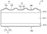
- the optical body 1 includes a substrate 10, a first micro uneven structure 11, a second micro uneven structure 12, and a macro uneven structure 13.
- the optical body 1 can function as a so-called light guide plate. That is, the optical body 1 emits internally propagating light incident on the optical body 1 from the side surface of the optical body 1 from the surface of the optical body 1 (specifically, a first surface 10A described later) to the outside.
- the base material 10 propagates the light incident on the inside of the base material 10, that is, internally propagated light, in the surface direction of the base material 10 (that is, the direction perpendicular to the thickness direction, the horizontal direction in FIG. 1). Further, although details will be described later, the optical body 1 is a macro uneven surface master having a reversed shape of the macro uneven structure 13 on the base material 10 on which the first micro uneven structure 11 and the second micro uneven structure 12 are formed. It is made by pressing under heating. Therefore, the base material 10 is required to be softened under heating. Therefore, it is preferable that the base material 10 is comprised with the thermoplastic resin excellent in light conductivity.
- the thickness of the substrate 10 is not particularly limited, and may be adjusted as appropriate depending on the use of the optical body 1 and the like.
- the substrate 10 may have a multilayer structure. For example, even if the optical body 1 is manufactured by bonding the base material on which the first micro uneven structure 11 is formed and the base material on which the second micro uneven structure 12 and the macro uneven structure 13 are formed, Good.
- the base material in which the 1st micro concavo-convex structure 11 was formed, the 2nd micro concavo-convex structure 12, and the macro concavo-convex structure 13 were formed in the both surfaces of the base material comprised with resin other than a thermoplastic resin. You may bond together a base material.
- the base material on which the second micro uneven structure 12 and the macro uneven structure 13 are formed is made of a thermoplastic resin.
- the first micro concavo-convex structure 11 is periodically formed in accordance with the surface 10A (hereinafter also referred to as the first surface) 10A of the substrate 10. That is, the first micro uneven structure 11 extends in a direction perpendicular to the first surface 10A.
- the average period of the concavo-convex is not more than the visible light wavelength (for example, 830 nm or less).
- the average period of the irregularities is preferably 100 nm or more and 350 nm or less, more preferably 120 nm or more and 280 nm or less, and further preferably 130 to 270 nm. Therefore, the first micro uneven structure 11 has a so-called moth-eye structure.
- the average period when the average period is less than 100 nm, it may be difficult to form the first micro uneven structure 11, which is not preferable. Further, when the average period exceeds 350 nm, the intensity of diffracted light may increase. That is, the internally propagating light may be diffracted by the first surface 10A and leaked to the outside.
- the first micro concavo-convex structure 11 has a large number of first micro convex portions 11a and first micro concave portions 11b.
- the first micro convex portion 11 a has a shape protruding outward in the thickness direction of the optical body 1
- the first micro concave portion 11 b has a shape recessed in the thickness direction of the optical body 1.
- the first micro convex portion 11a and the first micro concave portion 11b are periodically formed on the first surface 10A.
- the first micro concavo-convex structure 11 is a structure in which tracks (rows) composed of a plurality of first micro convex portions 11a and first micro concave portions 11b are arranged in parallel to each other.
- the tracks extend in the left-right direction and are aligned in the up-down direction.
- the first micro convex portion 11a (or the first micro concave portion 11b) disposed between adjacent tracks is half the length of the first micro convex portion 11a (or the first micro concave portion 11b). Only shifted in the track length direction.
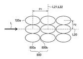
- the average period of the irregularities is given as an arithmetic average value of the dot pitch P1 and the track pitch P2.
- the dot pitch P1 is a distance between the first micro convex portions 11a (or the first micro concave portions 11b) arranged in the track length direction.
- the track pitch P2 is a distance between adjacent tracks. In this embodiment, both the dot pitch P1 and the track pitch P2 are less than or equal to the visible light wavelength.
- the dot pitch P1 and the track pitch P2 may be the same or different.
- the dot pitch P1 is a distance between the first micro convex portions 11a (or the first micro concave portions 11b) arranged in the track length direction.
- the first micro concavo-convex structure 11 can be observed by, for example, a scanning electron microscope (SEM) or a cross-sectional transmission electron microscope (cross-section TEM).
- the dot pitch P1 is measured by the following method, for example. That is, a combination of the first micro-projections 11a adjacent in the track length direction is picked up.
- the distance between the vertices of the first micro-projections 11a may be the dot pitch P1.
- the track pitch P2 is a distance between adjacent tracks.
- the track pitch P2 is measured by the following method, for example. That is, a combination of adjacent tracks is picked up.
- the distance between the tracks may be the track pitch P2.
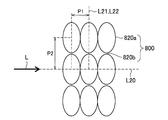
- the arrangement direction of the first micro concavo-convex structure 11 is divided into two arrangement directions, that is, a dot arrangement direction L20 and a cross arrangement direction L22.
- the dot arrangement direction L20 coincides with the track extending direction.
- the intersecting arrangement direction L22 is defined as a direction connecting the vertices of the first micro convex portions 11a (or the first micro concave portions 11b) adjacent to each other in the track arranging direction (here, the vertical direction).
- the angle between at least one of the dot arrangement direction L20 and the cross arrangement direction L21 and the straight line L21 perpendicular to the propagation direction L of the internal propagation light is 30 to 60 °. preferable.
- the angle ⁇ formed by the intersecting arrangement direction L22 and the straight line L21 is 30 to 60 °.
- the propagation direction L of the internal propagation light is defined as the propagation direction of the internal propagation light incident perpendicularly to the side surface of the substrate 10. Therefore, the propagation direction L is parallel to the surface direction of the substrate 10. Further, the plane whose normal is the propagation direction L and the surface direction of the substrate 10 intersect perpendicularly.
- the first micro concavo-convex structures 11 are arranged in a staggered pattern with respect to the traveling direction of the internally propagating light. That is, the traveling direction of the internal propagation light and the dot arrangement direction of the first micro concavo-convex structure 11 substantially coincide.
- the arrangement of the first micro uneven structure 11 is not limited to this example. That is, any arrangement is possible as long as the above-described requirements are satisfied.
- the first micro uneven structure 11 may be arranged in a rectangular lattice shape.
- the average height of the first micro uneven structure 11 is not particularly limited. That is, the average height of the first micro uneven structure 11 may be the same as or different from the average height of the second micro uneven structure 12.
- the average height of the first micro uneven structure 11 is preferably 100 nm to 300 nm, more preferably 130 nm. It is not less than 300 nm, more preferably not less than 150 nm and not more than 230 nm.
- the average height of the 1st micro uneven structure 11 is an arithmetic average value of the height of the 1st micro convex part 11a.
- the height of the 1st micro convex part 11a can be measured with the observation method mentioned above. That is, several heights of the first micro-projections 11 a are measured, and the arithmetic average value thereof may be set as the average height of the first micro-concave structure 11.
- the first micro convex portion 11a extends in a direction perpendicular to the first surface 10A.
- the second micro concavo-convex structure 12 is periodically formed along the surface (hereinafter also referred to as “second surface”) 10 ⁇ / b> B of the base material 10. That is, the second micro concavo-convex structure 12 extends in a direction perpendicular to the second surface 10B.
- the second micro uneven structure 12 has the same characteristics as the first micro uneven structure 11. That is, in the second micro concavo-convex structure 12, the average period of the concavo-convex is not more than the visible light wavelength (for example, 830 nm or less).
- the average period of the irregularities is preferably 100 nm or more and 350 nm or less, more preferably 120 nm or more and 280 nm or less, and further preferably 130 to 270 nm. Therefore, the second micro uneven structure 12 has a so-called moth-eye structure.
- the average period is less than 100 nm, it may be difficult to form the second micro uneven structure 12, which is not preferable.
- the average period exceeds 350 nm, the intensity of diffracted light may increase. That is, the internally propagating light may be diffracted by the second surface 10B and leaked to the outside.
- the second micro uneven structure 12 has a large number of second micro convex parts 12a and second micro concave parts 12b.
- the second micro convex portion 12 a has a shape protruding outward in the thickness direction of the optical body 1
- the second micro concave portion 12 b has a shape recessed in the thickness direction of the optical body 1.
- the second micro convex portion 12a and the second micro concave portion 12b are periodically formed on the second surface 10B.
- the arrangement of the second micro uneven structure 12 is the same as the arrangement of the first micro uneven structure 11.
- the arrangement direction of the second micro concavo-convex structure 12 is divided into two arrangement directions, that is, a dot arrangement direction L20 and a cross arrangement direction L22.
- an angle between at least one of the dot arrangement direction L20 and the cross arrangement direction L22 and a straight line L21 perpendicular to the propagation direction L of the internal propagation light is 30 to 60 °.
- the second micro uneven structure 12 is provided in both the region where the macro uneven structure 13 is formed, that is, the light emitting region 10D and the non-light emitting region 10C where the macro uneven structure 13 is not formed.
- the non-light emitting region 10C is a region other than the light emitting region 10D in the second surface 10B.
- the micro uneven structure 12 is formed following the surface of the non-light emitting region 10C. That is, the micro uneven structure 12 extends in a direction perpendicular to the surface of the non-light emitting region 10C.
- the macro uneven structure 13 is formed in the light emitting region 10D. Therefore, when light enters the optical body 1 from the light source 20, the internally propagated light is reflected by the macro uneven structure 13 in the light emitting region 10 ⁇ / b> D and emitted to the outside of the optical body 1. As a result, light is emitted from a region of the first surface 10A facing the light emitting region 10D. Accordingly, the light emitting region 10D is a region that emits internally propagating light. On the other hand, the macro uneven structure 13 is not formed in the non-light emitting region 10C. Therefore, light is not emitted from the region of the first surface 10A facing the non-light emitting region 10C.
- the second micro uneven structure 12 is formed following the surface of the macro uneven structure 13. That is, the second micro convex portion 12 a extends in a direction perpendicular to the surface of the macro uneven structure 13.
- the average height of the second micro uneven structure 12 is preferably 200 nm or more. Thereby, the antireflection function on the macro uneven structure 13 can be further enhanced.
- the upper limit value of the average height of the second micro concavo-convex structure 12 is not particularly limited, but is preferably 300 nm or less.
- the micro uneven structure 12 is provided in both the light emitting region 12D and the non-light emitting region 12C.
- the optical body 1 when used as a light guide plate, it is necessary to prevent the non-light emitting area from being recognized as much as possible by the viewer. Furthermore, it is necessary to prevent the viewer from recognizing the presence of the optical body 1 as much as possible when the light source is turned off. For this reason, in both the light emitting region 13D and the non-light emitting region 13C, an excellent antireflection function for extraneous light such as high transmission, low reflection, and low scattering is required. For this reason, in this embodiment, the micro uneven structure 12 is provided in both the light emitting region 12D and the non-light emitting region 12C.
- the first micro concavo-convex structure 11 and the second micro concavo-convex structure 12 may be integrally formed with the base material 10 or may be separate structures from the base material 10. Moreover, the uneven
- the macro uneven structure 13 is formed on a part of the second surface 10B.
- the macro uneven structure 13 is an aggregate of a plurality of macro convex portions 13a and macro concave portions 13b.
- the macro recess 13b has a shape that is recessed in the thickness direction of the optical body 1 with respect to the non-light emitting region 10C. Furthermore, the macro recessed part 13b may have what is called a prism shape. That is, the macro concave portion 13b is a long concave portion that extends in any plane direction of the second surface 10B (a direction perpendicular to the thickness direction of the optical body 1). In the example of FIG. 1, the macro recess 13b extends in a direction perpendicular to the paper surface.
- the shape of the macro recessed part 13b is not limited to this.
- the macro convex part 13a is arrange
- the vertices of the macro convex portions 13a are arranged in substantially the same plane as the non-light emitting region 10C. Therefore, although the details will be described later, the macro uneven structure 13 is formed by pressing a macro uneven surface master (see FIGS. 5 and 6) having an inverted shape of the macro recessed portion 13 b against the second micro uneven structure 12.
- the macro concave portion 13 b emits the internal propagation light toward the outside of the optical body 1. That is, the internally propagating light is reflected on the surface of the macro recess 13b.
- the specific shape of the macro uneven structure 13 is not particularly limited as long as it is the same shape as the macro uneven structure employed in the light guide plate.
- the macro recess 13b preferably has an inclined surface inclined with respect to the second surface 10B, and the angle ⁇ 1 formed by these is preferably 30 ° or more and less than 90 °.
- the macro concave portion 13b can emit the internal propagation light to the outside of the optical body 1 more reliably.
- the macro uneven structure 13 is formed on a part of the second surface 10B. For this reason, as described above, the second surface 10B is divided into a non-light emitting region 10C and a light emitting region 10D. Of course, the macro uneven structure 13 may be formed on the entire surface of the second surface 10B. In this case, the entire second surface 10B becomes the light emitting region 10D. In addition, the entire surface of the first surface 10A emits light.
- the shape of the macro uneven structure 13 is not limited to the example shown in FIG.
- the macro uneven structure 13 may have the inverted shape of FIG.
- the macro convex portion 13a has a shape protruding in the thickness direction of the optical body 1 with respect to the non-light emitting region 10C.
- the macro convex part 13a has what is called a prism shape.
- the internally propagating light is reflected by the surface of the macro convex portion 13a and is emitted to the outside of the optical body 1A.
- the angle formed between the inclined surface of the macro convex portion 13a and the second surface 10B is 30 ° or more and less than 90 °.
- the macro concave portion 13b can emit the internal propagation light to the outside of the optical body 1 more reliably.
- the micro concavo-convex structure 12 is formed following the inclined surface of the macro convex portion 13a.
- a micro uneven structure may be selectively formed only at least on the flat portions (here, the first surface 10A and the non-light emitting region 10C).
- the macro uneven structure 13 may not have a micro uneven structure.
- the luminous reflectance of the optical body 1, particularly the luminous reflectance of the light emitting region 10D is preferably 1.0% or less. Furthermore, it is preferable that the reflection chromaticity a * , b * of the optical body 1, particularly the reflection chromaticity a * , b * of the light emitting region 10D is 1.0 or less.
- the light emitting device includes the optical body 1 and the light source 20 described above.
- the operation of this light emitting device is roughly as follows. First, light enters the optical body 1 from the light source 20. The light incident on the inside of the optical body 1, that is, the internally propagating light is reflected by the first surface 10A and the second surface 10B of the optical body 1 (that is, the interface between the inside and the outside of the optical body 1). It propagates inside the optical body 1. Thereafter, the internally propagated light is reflected by the surface of the macro uneven structure 13 and is emitted from the other surface of the light guide plate. Thereby, the optical body 1 emits light.
- a straight line L10 indicates an example of an optical path of internally propagating light reflected by the surface of the macro uneven structure 13.
- the straight line L10 indicates an example of an optical path of internally propagating light that propagates inside the optical body 1.
- part of the internally propagated light may be emitted outside the optical body 1 as leaked light.
- the internally propagating light reaches the first surface 10A or the second surface 10B of the optical body 1, it may be diffracted and leaked to the outside.
- the internally propagating light propagates through the optical body 1 in various directions, and the wavelengths thereof are also various. For this reason, diffracted light (that is, leakage light) due to the arrangement of the first micro uneven structure 11 and the second micro uneven structure 12 tends to be a problem.
- the arrangement direction of the first micro uneven structure 11 and the second micro uneven structure 12 satisfies the above-described requirements, a lot of leaked light is emitted to a position different from the position of the viewer. Therefore, it is difficult for the viewer to visually recognize the leaked light. Therefore, for example, when the light-emitting device is used as a light-emitting device for LCD (so-called backlight or the like), the viewer can visually recognize a clearer image.
- the arrangement direction of the first micro concavo-convex structure 11 does not satisfy the above-described requirements, most of the leaked light leaking from the first surface 10A is emitted toward the viewer. For this reason, the viewer can easily see the leaked light. Therefore, for example, when the light-emitting device is used as a light-emitting device for an LCD (so-called backlight or the like), there is a possibility that the image is colored by leaking light. Accordingly, the visibility of the image is deteriorated. If the second micro concavo-convex structure 12 does not satisfy the above-described requirements, a similar event may occur on the second surface 10B.
- the optical body 1 has an excellent antireflection function for extraneous light, and can make it difficult for a viewer to visually recognize the leaked light. That is, in the present embodiment, it is possible to make it difficult for the viewer to visually recognize the leaked light generated in the non-light emitting region 10C, and thus the contrast between the light emitting region 10D and the non-light emitting region 10C can be improved.
- the non-light emitting area 10C looks black to the viewer, but this black color appears to be lumped.
- the first micro concavo-convex structure 11 can also suppress reflection inside the optical body 1, that is, reflection of internally propagated light. Therefore, more internal propagation light is emitted to the outside. Thereby, the optical body 1 can emit most of the internally propagating light reflected by the surface of the macro uneven structure to the outside. That is, the light extraction efficiency is improved.
- the first micro uneven structure 11 and the second micro uneven structure 12 are formed on both surfaces of the substrate 10.
- a micro uneven surface master 100 (see FIG. 4) having a reversed shape of the first micro uneven structure 11 and the second micro uneven structure 12 is prepared.
- an uncured resin layer is formed on both surfaces of the substrate 10.
- the uncured resin layer is composed of an uncured curable resin.
- the uncured resin layer is cured while transferring the micro uneven structure (specifically, the master uneven structure 120) of the micro uneven surface 100 to the uncured resin layer.
- the first micro uneven structure 11 and the second micro uneven structure 12 are formed on both surfaces of the substrate 10.
- the base material in which the 1st micro uneven structure 11 was formed may bond together the base material in which the 1st micro uneven structure 11 was formed, and the base material in which the 2nd micro uneven structure 12 was formed.
- a film in which the first micro uneven structure 11 and a film in which the second micro uneven structure 12 is formed may be bonded to the base material 10.
- the base material 10 is comprised with a thermoplastic resin, you may transfer the original recording uneven
- a master for macro unevenness On the surface of the master plate for macro unevenness, a macro uneven structure having an inverted shape of the macro uneven structure 13, specifically, a master macro convex portion having an inverted shape of the macro recessed portion 13 b is formed.
- the material of the master plate for macro unevenness is not particularly limited. For example, you may comprise with the material similar to the master 100 for micro unevenness
- the master for macro unevenness can be manufactured by the following steps. That is, a metal body whose surface is copper-plated or the like is cut with a cutting tool that has a symmetrical tip and a V shape, thereby producing a mold. The angle ⁇ 1 described above can be adjusted by adjusting the apex angle of the cutting tool.
- the angle ⁇ 1 is 45 °.
- the depth of the unevenness can be adjusted by the amount of pressing of the cutting tool.
- this mold is transferred to another material (that is, the material of the macro uneven master), thereby producing the macro uneven master.
- the transfer method is not particularly limited.
- the unevenness of the mold may be transferred to another metal material by electroforming.
- a cured resin layer made of UV curable resin or the like may be formed on the unevenness of the mold, and the resin layer may be cured.
- the pressure propagation medium may be any material as long as the pressure propagates.
- the pressure propagation medium may be compressed air, liquid, semi-solid semi-liquid viscoelastic body, and viscous body.
- the pressure is desirably 0.1 MPa or more, and more desirably 0.7 MPa or more.
- the heating temperature of the base material 10 and the master plate for macro unevenness is not particularly limited as long as the base material 10 can be deformed following the shape of the master macro protrusion.
- the heating temperature is preferably more than 150 ° C. and less than 250 ° C., more preferably 180 to 220 degrees. If the heating temperature is 150 ° C. or less, the shape of the base material 10 may not sufficiently follow the macro convex portions of the macro uneven master. Further, if the heating temperature exceeds 250 degrees, the substrate 10 may be damaged by heat.
- the pressure propagation medium is a viscous body, the pressure is 0.7 MPa, and the heating temperature is 180 to 220 ° C. According to this manufacturing method, an optical body in which the macro uneven structure 13 and the twelfth micro uneven structure 12 are formed in an overlapping manner is obtained.
- a new optical body 1 may be manufactured using the optical body 1 as a transfer mold.
- an uncured resin layer is formed on both surfaces of a new base material 10.
- the first micro uneven structure 11 may be transferred to one uncured resin layer
- the second micro uneven structure 12 and the macro uneven structure 13 may be transferred to the other uncured resin layer.
- the optical body 1A shown in FIG. 3 can be manufactured using the optical body 1 shown in FIG. 1 as a transfer mold.
- the first micro concavo-convex structure 11 and the second micro concavo-convex structure 12 are produced by using, for example, a micro concavo-convex master 100 shown in FIG. Next, the configuration of the micro uneven master 100 will be described.
- the micro uneven master 100 is, for example, a master used in the nanoimprint method, and has a cylindrical shape.
- the micro concave / convex master 100 may have a cylindrical shape or another shape (for example, a flat plate shape).
- the concave / convex structure 120 of the micro concave / convex master 100 can be seamlessly transferred to the substrate 10 by a roll-to-roll method. .
- the 1st micro uneven structure 11 and the 2nd micro uneven structure 12 can be formed on the base material 10 with high efficiency.
- the shape of the micro uneven master 100 is preferably cylindrical or columnar.
- the micro uneven master 100 includes a master base 110 and a master uneven structure 120 formed on the peripheral surface of the master base 110.
- the master base 110 may be, for example, a glass body, and specifically may be formed of quartz glass.
- the master base material 110 is not particularly limited as long as it has high SiO 2 purity, and may be formed of fused silica glass or synthetic quartz glass.
- the master base material 110 may be a metal base material obtained by laminating the above materials on a metal base material.
- the shape of the master base material 110 is a cylindrical shape, but may be a columnar shape or other shapes. However, as described above, the master base material 110 is preferably cylindrical or columnar.
- the master concavo-convex structure 120 has an inverted shape of the first micro concavo-convex structure 11 and the second micro concavo-convex structure 12.
- the 1st micro uneven structure 11 and the 2nd micro uneven structure 12 have a different shape, what is necessary is just to prepare the master plate for micro unevenness corresponding to these shapes.
- a base material resist layer is formed (film formation) on the master base material 110.
- the resist material constituting the base resist layer is not particularly limited, and may be either an organic resist material or an inorganic resist material.
- the organic resist material include novolak resists and chemically amplified resists.
- the inorganic resist material include metal oxides containing one or more transition metals such as tungsten (W) or molybdenum (Mo).
- the base resist layer is preferably formed of a thermal reaction resist containing a metal oxide.
- the base resist layer may be formed on the master base 110 by using spin coating, slit coating, dip coating, spray coating, screen printing, or the like. Moreover, when using an inorganic resist material for the base resist layer, the base resist layer may be formed by using a sputtering method.
- a latent image is formed on the base resist layer by exposing a part of the base resist layer with the exposure apparatus 200 (see FIG. 5). Specifically, the exposure apparatus 200 modulates the laser beam 200A and irradiates the substrate resist layer with the laser beam 200A. As a result, a part of the base resist layer irradiated with the laser beam 200A is denatured, so that a latent image corresponding to the master concavo-convex structure 120 can be formed on the base resist layer.
- the latent image is formed on the base resist layer with an average period equal to or shorter than the visible light wavelength.
- the base resist layer is developed by dropping a developer on the base resist layer on which the latent image is formed. Thereby, an uneven structure is formed in the base resist layer.
- the master base material 110 and the base material resist layer are etched using the base material resist layer as a mask, thereby forming the master concavo-convex structure 120 on the master base material 110.
- the etching method is not particularly limited, but dry etching having vertical anisotropy is preferable, for example, reactive ion etching (RIE) is preferable.
- RIE reactive ion etching
- the micro uneven master 100 is produced.
- An anodized porous alumina obtained by anodizing aluminum may be used as a master.
- Anodized porous alumina is disclosed in, for example, International Publication No. 2006/059686.
- the micro uneven master 100 may be manufactured by a stepper using an asymmetric reticle mask.
- a desired master uneven structure 120 can be formed.
- the shape of the master concavo-convex structure 120 can be changed to the inverted shape of the first micro concavo-convex structure 11 and the second micro concavo-convex structure 12.
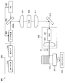
- the exposure apparatus 200 is an apparatus that exposes the base resist layer.
- the exposure apparatus 200 includes a laser light source 201, a first mirror 203, a photodiode (PD) 205, a deflection optical system, a control mechanism 230, a second mirror 213, a moving optical table 220, and a spindle motor. 225 and a turntable 227. Further, the master base material 110 is placed on the turntable 227 and can rotate.
- the laser light source 201 is a light source that emits laser light 200A, and is, for example, a solid-state laser or a semiconductor laser.
- the wavelength of the laser light 200A emitted from the laser light source 201 is not particularly limited, but may be, for example, a blue light band wavelength of 400 nm to 500 nm.
- the spot diameter of the laser beam 200A (the diameter of the spot irradiated on the resist layer) may be smaller than the diameter of the opening surface of the concave portion of the master concavo-convex structure 120, for example, about 200 nm.
- the laser beam 200 ⁇ / b> A emitted from the laser light source 201 is controlled by the control mechanism 230.
- the laser beam 200A emitted from the laser light source 201 travels straight in a parallel beam, is reflected by the first mirror 203, and is guided to the deflection optical system.
- the first mirror 203 is composed of a polarization beam splitter, and has a function of reflecting one of the polarization components and transmitting the other of the polarization components.
- the polarization component transmitted through the first mirror 203 is received by the photodiode 205 and subjected to photoelectric conversion.
- the light reception signal photoelectrically converted by the photodiode 205 is input to the laser light source 201, and the laser light source 201 performs phase modulation of the laser light 200A based on the input light reception signal.
- the deflection optical system includes a condenser lens 207, an electro-optic deflector (EOD) 209, and a collimator lens 211.
- EOD electro-optic deflector
- the laser beam 200A is condensed on the electro-optic deflection element 209 by the condenser lens 207.
- the electro-optic deflection element 209 is an element that can control the irradiation position of the laser light 200A.
- the exposure apparatus 200 can also change the irradiation position of the laser beam 200A guided onto the moving optical table 220 by the electro-optic deflection element 209 (so-called wobble mechanism).
- the laser beam 200 ⁇ / b> A is converted into a parallel beam again by the collimator lens 211 after the irradiation position is adjusted by the electro-optic deflection element 209.
- the laser light 200 ⁇ / b> A emitted from the deflection optical system is reflected by the second mirror 213 and guided horizontally and parallel onto the moving optical table 220.
- the moving optical table 220 includes a beam expander (BEX) 221 and an objective lens 223.
- the laser beam 200 ⁇ / b> A guided to the moving optical table 220 is shaped into a desired beam shape by the beam expander 221, and then irradiated to the substrate resist layer formed on the master substrate 110 through the objective lens 223. Is done. Further, the moving optical table 220 moves by one feed pitch (track pitch) in the arrow R direction (feed pitch direction) every time the master base 110 rotates once.
- the master base material 110 is installed on the turntable 227.
- the spindle motor 225 rotates the master base 110 by rotating the turntable 227. Thereby, the laser beam 200A is scanned on the base resist layer.
- a latent image of the base material resist layer is formed along the scanning direction of the laser beam 200A. Accordingly, the track direction (that is, the arrow B direction) of the first micro concavo-convex structure 11 and the second micro concavo-convex structure 12 corresponds to the scanning direction of the laser light 200A.
- the control mechanism 230 includes a formatter 231 and a driver 233, and controls the irradiation with the laser light 200A.
- the formatter 231 generates a modulation signal for controlling the irradiation of the laser light 200A, and the driver 233 controls the laser light source 201 based on the modulation signal generated by the formatter 231. Thereby, irradiation of the laser beam 200A to the master base material 110 is controlled.
- the formatter 231 generates a control signal for irradiating the substrate resist layer with the laser light 200A based on an input image on which an arbitrary pattern drawn on the substrate resist layer is drawn. Specifically, first, the formatter 231 acquires an input image on which an arbitrary pattern to be drawn on the base material resist layer is drawn. The input image is an image corresponding to a developed view of the outer peripheral surface of the base resist layer, which has been cut open in the axial direction and extended to one plane. Next, the formatter 231 divides the input image into small areas of a predetermined size (for example, in a grid pattern), and determines whether each small area includes a drawing pattern.
- a predetermined size for example, in a grid pattern
- the formatter 231 generates a control signal that controls to irradiate the laser light 200 ⁇ / b> A to each small region that is determined to include a drawing pattern.
- the control signal (that is, the exposure signal) is preferably synchronized with the rotation of the spindle motor 225, but may not be synchronized. Further, the synchronization between the control signal and the rotation of the spindle motor 225 may be reset every time the master base material 110 rotates once.
- the driver 233 controls the output of the laser light source 201 based on the control signal generated by the formatter 231. Thereby, irradiation of the laser beam 200A to the base resist layer is controlled.
- the exposure apparatus 200 may perform known exposure control processing such as focus servo, position correction of the irradiation spot of the laser beam 200A, and the like.
- the focus servo may use the wavelength of the laser beam 200A, or may use another wavelength for reference.
- the laser beam 200A irradiated from the laser light source 201 may be irradiated to the base resist layer after being branched into a plurality of optical systems. In this case, a plurality of irradiation spots are formed on the base resist layer. In this case, the exposure may be terminated when the laser beam 200A emitted from one optical system reaches the latent image formed by the other optical system.
- the transfer device 300 includes a micro uneven master 100, a substrate supply roll 301, a winding roll 302, guide rolls 303 and 304, a nip roll 305, a peeling roll 306, a coating apparatus 307, and a light source 309. Prepare.
- the base material supply roll 301 is a roll in which the long base material 10 is wound in a roll shape
- the winding roll 302 is a roll that winds up the base material 10 on which the first micro uneven structure is formed.
- the guide rolls 303 and 304 are rolls that transport the base material 10.
- the nip roll 305 is a roll for bringing the base material 10 on which the uncured resin layer 310 is laminated, that is, the transferred film 3a into close contact with the master plate 100 for micro unevenness.
- the peeling roll 306 is a roll for peeling the base material 10 on which the first micro uneven structure 11 is formed from the micro uneven surface master 100.
- the coating device 307 includes coating means such as a coater, and applies an uncured photocurable resin composition to the substrate 10 to form an uncured resin layer 310.
- the kind in particular of photocurable resin composition is not restrict
- the coating device 307 may be, for example, a gravure coater, a wire bar coater, or a die coater.
- the light source 309 is a light source that emits light having a wavelength capable of curing the photocurable resin composition, and may be, for example, an ultraviolet lamp.
- the base material 10 is continuously sent out from the base material supply roll 301 through the guide roll 303.
- the uncured photocurable resin composition is applied to the delivered base material 10 by the coating device 307, and the uncured resin layer 310 is laminated on the base material 10.
- the to-be-transferred film 3a is produced.
- the transferred film 3a is brought into close contact with the master 100 for micro unevenness by a nip roll 305.
- the light source 309 cures the uncured resin layer 310 by irradiating light to the uncured resin layer 310 in close contact with the micro uneven master 100.
- the master uneven structure 120 formed on the outer peripheral surface of the micro uneven master 100 is transferred to the uncured resin layer 310.
- the first micro concavo-convex structure 11 having the inverted shape of the master concavo-convex structure 120 is formed on the substrate 10.
- the base material 10 on which the first micro concavo-convex structure 11 is formed is peeled off from the micro uneven surface master 100 by the peeling roll 306.
- the base material 10 is taken up by the take-up roll 302 via the guide roll 304.
- the micro uneven master 100 may be placed vertically or horizontally, and a mechanism for correcting the rotation angle and eccentricity of the micro uneven master 100 may be provided separately.
- an eccentric tilt mechanism may be provided in the chucking mechanism.
- the transfer film 3a is transported by roll-to-roll, while the peripheral shape of the micro uneven master 100 is transferred to the transfer film 3a.
- the first micro uneven structure 11 is formed on the substrate 10.
- the master uneven structure 120 of the micro uneven master 100 may be directly transferred onto the base 10.
- the coating device 307 and the light source 309 are unnecessary.
- a heating device is disposed upstream of the micro uneven master 100. The base material 10 is heated and softened by this heating device, and then the base material 10 is pressed against the master plate 100 for micro unevenness. Accordingly, the master uneven structure 120 formed on the peripheral surface of the micro uneven master 100 is transferred to the substrate 10. Therefore, the transfer device 300 can continuously form the first micro uneven structure 11 on the substrate 10.
- a transfer film in which the master uneven structure 120 of the micro uneven master 100 is transferred may be used as a transfer mold.
- the micro uneven master 100 may be duplicated by electroforming or thermal transfer, and this duplicate may be used as a transfer mold.
- the shape of the micro uneven master 100 need not be limited to a roll shape, and may be a flat master.
- Various processing methods such as anodization can be selected.
- FIG. 7 shows a configuration of the optical body 1-1 according to the first embodiment.
- the optical body 1-1 was produced by the following steps. First, a polymethyl methacrylate film (Technoloy manufactured by Sumika Acrylic Sales Co., Ltd.) having a thickness of 150 ⁇ m was prepared as the substrate 10-1. Next, the second micro uneven structure 12 was formed on one surface (here, the second surface 10B) of the substrate 10-1 using the transfer apparatus 300 shown in FIG.
- an ultraviolet curable acrylic resin composition (SK1120 manufactured by Dexerials) was used as the photocurable resin composition.
- the second surface 10B of the substrate 10-1 was previously primed in order to improve the adhesion between the substrate 10-1 and the cured layer of the uncured resin layer.
- a primer layer having a thickness of about 3 ⁇ m was formed on the second surface 10B of the substrate 10-1 by the primer treatment. Specifically, the primer treatment was performed by applying and drying a polycarbonate resin.
- the second micro uneven structures 12 were arranged in a staggered pattern.
- the dot pitch P1 was 230 nm and the track pitch P2 was 153 nm.
- the average height of the second micro-projections 12a was 250 nm.
- the substrate 10-1 was a long rectangular film.
- the dot arrangement direction L20 was parallel to the longitudinal direction of the substrate 10-1, and the intersecting arrangement direction L22 was inclined by about 40 ° with respect to a straight line perpendicular to the dot arrangement direction L20.
- An SEM photograph of the cross-sectional shape of the second micro uneven structure 12 is shown in FIG.
- a planar SEM photograph is shown in FIG.
- the master macro convex portion was a convex portion extending in the short direction of the macro concave / convex master disc, the pitch (distance between the vertices of the master macro convex portion) was 100 ⁇ m, and the height was 10 ⁇ m.
- the apex angle was 90 °. Therefore, the angle formed by the slope of the master macro convex portion and the plane between the master macro convex portions (that is, the bottom surface of the master macro concave portion) is 45 °.
- the master macro convex portion was transferred to the base material 10-1 by the method described above.
- the pressure propagation medium was a viscous body, the pressure was 0.7 MPa, and the heating temperature was 180 to 220 ° C. That is, the second micro uneven structure 12 and the macro uneven structure 13 were formed so as to overlap each other on the second surface of the substrate 10-1.
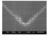
- FIG. 12 is a cross-sectional SEM photograph of the macro recess 13b. As is apparent from this photograph, it was confirmed that the second micro uneven structure 12 was formed so as to overlap on the macro recess 13b.
- the second micro convex portion 12a protrudes in the vertical direction from the surface of the macro concave portion 13b. That is, it was also confirmed that the second micro convex portion 12a was formed following the surface of the macro concave portion 13b.
- the moth-eye film 10-3 was attached to the other surface of the substrate 10-1, that is, the first surface 10A via a 25 ⁇ m thick adhesive film 10-2 (PANAC PDS1 film).
- a first micro uneven structure 11 is formed on the moth-eye film 10-3.
- the moth-eye film 10-3 was produced using the transfer device 300 described above. Specifically, a 60 ⁇ m-thick triacetyl cellulose film was used as the substrate, and an ultraviolet curable acrylic resin composition manufactured by Toagosei Co., Ltd. was used as the photo-curable resin composition.
- the thickness of the hardened layer on which the first micro uneven structure 11 is formed is about 3 ⁇ m.
- the uneven pattern of the first micro uneven structure 11 was the same as that of the second micro uneven structure 12.
- the optical body 1-1 according to Example 1 was manufactured through the above steps.
- the optical body 1-1 corresponds to the optical body 1 shown in FIG.
- spectral specular reflection spectrum was measured.
- the measurement of the regular reflection spectrum mainly evaluates the reflection characteristics of the flat portion of the optical body 1-1.
- Spectral specular reflection spectrum was measured using a spectrophotometer (model V-550, with absolute reflectance measurement unit, manufactured by JASCO Corporation). The incident angle and the reflection angle were both 5 °, the wavelength range was 400 to 800 nm, and the wavelength resolution was 1 nm. Further, the measurement light was applied to the second surface 10B. The results are shown in FIG.
- the horizontal axis in FIG. 20 indicates the measurement wavelength (nm), and the vertical axis indicates the regular reflectance (%).
- the diffuse reflection spectrum of the optical body 1-1 was measured.
- the measurement of the diffuse reflection spectrum is to evaluate the reflection characteristics on the entire surface of the optical body 1-1 including the macro uneven structure 13.
- the diffuse reflectance spectrum was measured by using the spectrophotometer (model V-550, with absolute reflectance measurement unit, manufactured by JASCO Corporation) and the absolute reflectance measuring instrument ARV474S (produced by JASCO Corporation) in combination. .
- Other conditions were the same as the measurement conditions for the specular reflection spectrum.
- a diffuse reflection spectrum is shown in FIG.
- the horizontal axis in FIG. 21 indicates the measurement wavelength (nm), and the vertical axis indicates the diffuse reflectance (%).
- a luminance meter (CS1000 manufactured by Konica Minolta Co., Ltd.) was installed on the surface 10A side of the first surface 10A, the installation position was 50 cm away from the first surface 10A, and the optical axis of the luminance meter was perpendicular to the first surface.
- High-intensity white light was incident on the optical body 1-1 from the LED light source, and the luminance (cd / cm 2 ) and xy value were measured with a luminance meter, which is perpendicular to the propagation direction L of the internal propagation light in Example 1.
- the angle formed between the straight line L21 and the intersecting arrangement direction L22 is 40 °, and the results are shown in Table 1.
- FIG. 8 shows a configuration of the optical body 1-2 according to the second embodiment.
- the optical body 1-2 was produced by using the optical body 1-1 as a transfer mold. Specifically, first, the base material 10-1 used in Example 1 was prepared. Subsequently, in order to improve the adhesion between the substrate 10-1 and each cured layer described later, both surfaces of the substrate 10-1 were subjected to primer treatment. The specific content of the primer treatment was the same as in Example 1. A primer layer having a thickness of about 3 ⁇ m was formed on both surfaces of the substrate 10-1 by the primer treatment. Next, an uncured resin layer of the photocurable resin composition was formed on one surface (here, the second surface 10B) of the substrate 10-1.
- the shape of the second surface 10B of the optical body 1-1 that is, the second micro uneven structure 12 and the macro uneven structure 13 were transferred to the uncured resin layer.
- the first macro uneven cured layer 10-5 was formed on the second surface 10B of the base material 10-1.
- the thickness of the first macro uneven cured layer 10-5 was about 3 ⁇ m.
- a second micro uneven structure 12 and a macro uneven structure 13 are formed in the first macro uneven cured layer 10-5.
- these 2nd micro uneven structure 12 and the macro uneven structure 13 have the reverse shape of the 2nd micro uneven structure 12 and the macro uneven structure 13 of Example 1.
- an uncured resin layer of the photocurable resin composition was formed on the other surface of the substrate 10-1, that is, the first surface 10A.
- the shape of the first surface 10A of the optical body 1-1, that is, the first micro uneven structure 11 was transferred to the uncured resin layer.
- a first micro uneven hardened layer 10-6 was formed on the first surface 10A of the substrate 10-1.
- the thickness of the first micro concave-convex cured layer 10-6 was about 3 ⁇ m.
- a first micro uneven structure 11 is formed in the first micro uneven cured layer 10-6.
- the first micro uneven structure 11 has an inverted shape of the first micro uneven structure 11 of the first embodiment.
- the optical body 1-2 according to Example 2 was manufactured through the above steps.
- the optical body 1-2 corresponds to the optical body 1A shown in FIG.
- Example 2 (2-2. Characteristic evaluation) Subsequently, the characteristics of the optical body 1-2 were evaluated in the same manner as in Example 1. A regular reflection spectrum is shown in FIG. 20, and a diffuse reflection spectrum is shown in FIG. In addition, Table 1 shows luminance and xy values. Further, Table 2 shows luminous reflectance and reflection chromaticity a * , b * .
- FIG. 9 illustrates a configuration of the optical body 1-3 according to the third embodiment.
- the optical body 1-3 was produced by using the optical body 1-2 as a transfer mold. Specifically, first, the base material 10-1 used in Example 1 was prepared. Subsequently, in order to improve the adhesion between the substrate 10-1 and each cured layer described later, both surfaces of the substrate 10-1 were subjected to primer treatment. The specific content of the primer treatment was the same as in Example 1. A primer layer having a thickness of about 3 ⁇ m was formed on both surfaces of the substrate 10-1 by the primer treatment.
- an uncured resin layer of the photocurable resin composition was formed on one surface (here, the second surface 10B) of the substrate 10-1.
- the shape of the second surface 10B of the optical body 1-2 that is, the second micro uneven structure 12 and the macro uneven structure 13 were transferred to the uncured resin layer.
- the second macro uneven cured layer 10-8 was formed on the second surface 10B of the base material 10-1.
- the thickness of the second macro uneven cured layer 10-8 was about 3 ⁇ m.
- a second micro uneven structure 12 and a macro uneven structure 13 are formed in the second macro uneven cured layer 10-8.
- these 2nd micro uneven structure 12 and the macro uneven structure 13 have the reverse shape of the 2nd micro uneven structure 12 and the macro uneven structure 13 of Example 2.
- FIG. That is, the second micro uneven structure 12 and the macro uneven structure 13 of Example 3 have substantially the same shape as the second micro uneven structure 12 and macro uneven structure 13 of Example 1.
- an uncured resin layer of the photocurable resin composition was formed on the other surface of the substrate 10-1, that is, the first surface 10A.
- the shape of the first surface 10A of the optical body 1-2 that is, the first micro uneven structure 11 was transferred to the uncured resin layer.
- a second micro uneven hardened layer 10-9 was formed on the first surface 10A of the base material 10-1.
- the thickness of the second micro uneven hardened layer 10-9 was about 3 ⁇ m.
- a first micro uneven structure 11 is formed in the second micro uneven cured layer 10-9.
- the first micro uneven structure 11 has an inverted shape of the first micro uneven structure 11 of the second embodiment. That is, the first micro uneven structure 11 of Example 3 has substantially the same shape as the first micro uneven structure 11 of Example 1.
- the optical body 1-3 according to Example 3 was manufactured through the above steps.
- the optical body 1-3 corresponds to the optical body 1 shown in FIG.
- Example 2 (3-2. Characteristic evaluation) Subsequently, the characteristics of the optical body 1-3 were evaluated in the same manner as in Example 1. A regular reflection spectrum is shown in FIG. 20, and a diffuse reflection spectrum is shown in FIG. In addition, Table 1 shows luminance and xy values. Further, Table 2 shows luminous reflectance and reflection chromaticity a * , b * .
- FIG. 13 shows a configuration of an optical body 500 according to Comparative Example 1.
- the optical body 500 was manufactured through the following steps. First, a substrate 510 similar to the substrate 10-1 used in Example 1 was prepared. Next, the macro uneven structure 520 was formed on the surface of the substrate 510 using the macro uneven master used in Example 1.
- the macro concavo-convex structure 520 includes a macro convex portion 520a and a macro concave portion 520b, and the macro concave portion 520b has an inverted shape of the master macro convex portion.
- the optical body 500 which concerns on the comparative example 1 was produced according to the above process.
- Example 2 (4-2. Characteristic evaluation) Subsequently, the characteristic evaluation of the optical body 500 was performed in the same manner as in Example 1. A regular reflection spectrum is shown in FIG. 20, and a diffuse reflection spectrum is shown in FIG. In addition, Table 1 shows luminance and xy values. Further, Table 2 shows luminous reflectance and reflection chromaticity a * , b * .
- FIG. 14 shows a configuration of an optical body 600 according to Comparative Example 2.
- the optical body 600 was produced by attaching the moth-eye film 620 to the back surface of the optical body 500 (that is, the surface on the side where the macro uneven structure 520 is not formed) via the adhesive film 610.
- the adhesive film 610 and the moth-eye film 620 were the same as the adhesive film 10-2 and the moth-eye film 10-3 used in Example 1.
- Example 2 (5-2. Characteristic evaluation) Subsequently, the characteristic evaluation of the optical body 600 was performed in the same manner as in Example 1. A regular reflection spectrum is shown in FIG. 20, and a diffuse reflection spectrum is shown in FIG. In addition, Table 1 shows luminance and xy values. Further, Table 2 shows luminous reflectance and reflection chromaticity a * , b * .
- FIG. 15 shows a configuration of an optical body 700 according to Comparative Example 3.
- an optical body 700 was manufactured by attaching an antireflection film 720 having a thickness of 60 ⁇ m to both surfaces of the optical body 500 via an adhesive film 710.
- the adhesive film 610 was the same as the adhesive film 10-2 used in Example 1.
- the antireflection film 720 was an AR film of inorganic four-layer film manufactured by Dexerials.
- Example 2 (5-2. Characteristic evaluation) Subsequently, the characteristic evaluation of the optical body 600 was performed in the same manner as in Example 1. A regular reflection spectrum is shown in FIG. 20, and a diffuse reflection spectrum is shown in FIG. In addition, Table 1 shows luminance and xy values. Further, Table 2 shows luminous reflectance and reflection chromaticity a * , b * .
- Example 2 the luminance in Examples 1 and 3 was superior to that in Example 2.
- the macro concave portion 13b which is a reflection portion of the internally propagating light is engraved in the optical bodies 1-1 and 1-3. For this reason, much of the internally propagating light traveling in the direction perpendicular to the thickness direction of the optical bodies 1-1 and 1-3, that is, so-called parallel light hits the film and the recess 13b and is totally reflected.
- the macro convex portion 13a which is a reflection portion of the internally propagating light, projects outward in the thickness direction of the optical body 1-2. For this reason, it becomes difficult for the parallel light to hit the macro convex portion 13a. For this reason, it is considered that the luminance in Examples 1 and 3 was superior to that in Example 2.
- an optical body 1-1A obtained by removing the macro uneven structure 13 from the optical body 1-1 described above was prepared as an optical body corresponding to the present embodiment.
- This optical body 1-1A was produced by removing the process of the master plate for macro unevenness from the process of producing the optical body 1-1.
- a comparative optical body Comparative Example 4
- optical body 1-1B such an optical body is also referred to as “optical body 1-1B”).
- the micro concavo-convex structure 800 has a large number of micro convex portions 800a and micro concave portions 800b.
- the optical body 1-1B was produced by changing the master uneven structure 120 of the master 100 for micro unevenness of the transfer device 300.
- the dot pitch P1, the track pitch P2, and the average height of the micro concavo-convex structure 800 were the same as those of the first micro concavo-convex structure 11 and the second micro concavo-convex structure 12 of Example 1.
- the arrangement was a lattice arrangement, and the dot arrangement direction L20 was a direction parallel to the longitudinal direction of the optical body 1-1B.
- a planar SEM photograph of the micro uneven structure 800 is shown in FIG.
- optical body 1-1D having a micro concavo-convex structure arranged in the above is prepared.
- Such a micro uneven structure was produced by changing the master uneven structure 120 of the micro uneven master 100 of the transfer device 300.
- the master plate 100 for micro unevenness was produced by randomly changing the irradiation interval of the laser light 200 ⁇ / b> A when performing exposure using the exposure apparatus 200.
- the average period of the micro concavo-convex structure was 200 nm.
- the same experiment as the above-described measurement of luminance and xy value was performed.
- the angle formed by the straight line L21 perpendicular to the propagation direction L of the internal propagation light and the intersecting arrangement direction L22 is 40 °.
- the angle formed by the straight line L21 perpendicular to the propagation direction L of the internal propagation light and the intersecting arrangement direction L22 is 0 °.
- the arrangement direction cannot be defined.
- the luminance of the optical body 1-1A is 8.5 cd / m 2
- the luminance of the optical body 1-1B is 9.2 cd / m 2
- the luminance of the optical body 1-1C is 12.3 cd / m 2. 2 .
- a similar experiment was performed by further setting the position of the LED light source on the side surface on the longitudinal side of the optical body 1-1B.
- the wave 17 shows the correspondence between the propagation direction L at this time, the dot arrangement direction L20, and the cross arrangement direction L22. Even in this case, the angle formed by the straight line L21 perpendicular to the propagation direction L of the internal propagation light and the intersecting arrangement direction L22 is 0 °.
- the luminance of the optical body 1-1B was 9.7 cd / m 2 . Therefore, the luminance of the optical body 1-1A was the smallest.
- the micro uneven structure needs to be periodically arranged, and the intersecting arrangement direction L22 is relative to the straight line L21 perpendicular to the propagation direction L of the internal propagation light. It has been found that it is necessary to incline and the angle needs to be 30-60 ° C.
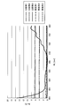
- the incident angle was changed within the range of 0 to 70 °, and the measurement wavelength was set to 380 nm to 780 nm. It was.
- the reflection angle was the same value as the incident angle.
- the same process was performed by changing the average height of the first micro uneven structure 11 (specifically, the average height of the first micro protrusion 11a).
- the luminous reflectance (that is, the Y value in the Yxy color space) was measured. The results are shown in FIG.
- the horizontal axis in FIG. 22 indicates the incident angle of the measurement light, and the vertical axis indicates the luminous reflectance (reflection Y value).
- a small luminous reflectance in this range means that the luminous reflectance on the macro uneven structure 13 is also small. In this respect, it was found that the luminous reflectance is sufficiently small when the average height is 200 nm or more.
Abstract
【課題】導光板として使用可能であり、かつ、外来光に対する優れた反射防止機能を有する発光装置を提供する。 【解決手段】上記課題を解決するために、本発明のある観点によれば、基材と、基材の一方の表面に形成され、基材の側面から基材の内部に入射された内部伝播光を基材の他方の表面から出射するマクロ凹凸構造と、基材の両面及びマクロ凹凸構造の表面にならって周期的に形成され、凹凸の平均周期が可視光波長以下であるミクロ凹凸構造と、を含み、 マクロ凹凸構造の表面は、一方の表面に対して30°以上90°未満で傾斜した傾斜面を有し、ミクロ凹凸構造の配列は内部伝播光の進行方向に対して千鳥配列で配置されている光学体が提供される。
Description
本発明は、光学体及び発光装置に関する。
光学体の一種として、光の導波現象及びマクロ凹凸構造を組み合わせた光学体が知られている。このような光学体は、導光板とも称される。マクロ凹凸構造は、導光板の一方の表面に形成される。そして、導光板の内部には、導光板の側面に設けられた光源から光が入射される。導光板の内部に入射された光、すなわち内部伝播光は、導光板の表面(すなわち、導光板の内部と外部との界面)で反射しながら導光板の内部を伝播する。その後、内部伝播光は、マクロ凹凸構造の表面で反射し、導光板の他方の表面から出射される。すなわち、導光板は、導光板の側面から入射された光を導光板の表面から出射する。導光板は、例えば各種の表示装置用の発光体、あるいは照明用の発光体として用いられる。導光板が使用される表示装置としては、例えば、各種LCD(例えば、ローカルディミング駆動方式のLCD)、パッシブタイプ表示装置、アミューズメント向けの光装飾パネルやデジタルサイネージ等の広告向けのイルミパネル等が挙げられる。これらの表示装置では、光源の点灯と消灯により、マクロ凹凸構造のパターンが形成された箇所からあたかも光が浮き上がるような表現が可能となる。
導光板が表示装置の発光体として使用される場合、マクロ凹凸構造の少なくとも一方の面の斜面は30°以上90°未満の斜面が必要である。導光板の側面から入射し、導光板内を進行した光はこの斜面により全反射し導光板の表面から出射する。さらにこのような導光板では、光源を消灯した際に視認者に導光板の存在をなるべく認識させないようにする必要がある。さらに、表示品質を高くする必要がある。このため、高透過、低反射、かつ低散乱という外来光に対する優れた反射防止機能が求められる。表示装置の表示品質を高くするためである。ここで、外来光としては、太陽光、他の発光体(例えば、照明、他の表示装置等)からの光の他、表示装置内部に設けられた他の表示体(例えば液晶パネル等)等からの光も挙げられる。
しかし、上述した要求に十分に応える技術は何ら提案されていなかった。例えば、特許文献1~3には、上述した導光板に関する技術が開示されている。特許文献1に開示された技術では、導光板の両面のうち、少なくとも一方の表面に凹凸の平均周期が可視光波長以下であるミクロ凹凸構造を設ける。ここで、ミクロ凹凸構造は、ランダムに配置される。また、ミクロ凹凸構造の凸部間距離または凹部間距離が所定の条件を満たす。
特許文献2に開示された技術では、マクロ凹凸構造の凹部間の所定位置に光反射角制御面を形成する。特許文献3に開示された技術では、導光板の両面のうち、少なくとも一方の表面に多層構造の反射防止膜を設ける。しかし、これらの技術では、上述した要求に十分に応えることができなかった。このため、上述した要求に十分に応える技術が強く切望されていた。
そこで、本発明は、上記問題に鑑みてなされたものであり、本発明の目的とするところは、導光板として使用可能であり、かつ、外来光に対する優れた反射防止機能を有することが可能な、新規かつ改良された光学体及び発光装置を提供することにある。
上記課題を解決するために、本発明のある観点によれば、基材と、基材の一方の表面に形成され、基材の側面から基材の内部に入射された内部伝播光を基材の他方の表面から出射するマクロ凹凸構造と、基材の両面及びマクロ凹凸構造の表面にならって周期的に形成され、凹凸の平均周期が可視光波長以下であるミクロ凹凸構造と、を含み、
マクロ凹凸構造の表面は、一方の表面に対して30°以上90°未満で傾斜した傾斜面を有し、ミクロ凹凸構造の配列は内部伝播光の進行方向に対して千鳥配列で配置されている光学体が提供される。
マクロ凹凸構造の表面は、一方の表面に対して30°以上90°未満で傾斜した傾斜面を有し、ミクロ凹凸構造の配列は内部伝播光の進行方向に対して千鳥配列で配置されている光学体が提供される。
ここで、ミクロ凹凸構造の配列方向と、内部伝播光の伝播方向に垂直な方向とのなす角度が30~60°であってもよい。
また、一方の表面は、マクロ凹凸構造が形成された発光領域と、発光領域以外の非発光領域とに区分され、ミクロ凹凸構造は、発光領域及び非発光領域の両方に形成されてもよい。
また、ミクロ凹凸構造は、マクロ凹凸構造の表面に対して垂直な方向に伸びていてもよい。
また、マクロ凹凸構造は、複数のマクロ凸部及びマクロ凹部の集合体となっており、かつ、複数のマクロ凸部及びマクロ凹部の少なくとも一方はプリズム形状を有し、ミクロ凹凸構造は、複数のマクロ凸部及びマクロ凹部の各々の表面にならって形成されてもよい。
また、視感反射率は1.0%以下であってもよい。
また、さらに反射色度a*、b*が1.0以下であってもよい。
また、ミクロ凹凸構造の平均高さは200nm以上であってもよい。
また、基材は、多層構造を有していてもよい。
本発明の他の観点によれば、上記の光学体と、光学体の側面に設けられ、光学体の側面から光学体の内部に光を入射する光源と、を備える、発光装置が提供される。
以上説明したように本発明によれば、光学体の表面に形成されたマクロ凹凸構造は、基材の側面から基材の内部に入射された内部伝播光を基材の他方の表面から出射することができる。したがって、光学体を導光板として使用することができる。さらに、ミクロ凹凸構造は、基材の両面及びマクロ凹凸構造の表面にならって周期的に形成され、凹凸の平均周期が可視光波長以下となっている。したがって、光学体は、外来光に対する優れた反射防止機能を有する。
以下に添付図面を参照しながら、本発明の好適な実施の形態について詳細に説明する。なお、本明細書及び図面において、実質的に同一の機能構成を有する構成要素については、同一の符号を付することにより重複説明を省略する。
<1.光学体の構成>
次に、図1及び図2に基づいて、本実施形態に係る光学体1の構成について説明する。光学体1は、基材10と、第1のミクロ凹凸構造11と、第2のミクロ凹凸構造12と、マクロ凹凸構造13と、を備える。光学体1は、いわゆる導光板として機能しうる。すなわち、光学体1は、光学体1の側面から光学体1に入射された内部伝播光を光学体1の表面(具体的には、後述する第1の表面10A)から外部に出射する。
次に、図1及び図2に基づいて、本実施形態に係る光学体1の構成について説明する。光学体1は、基材10と、第1のミクロ凹凸構造11と、第2のミクロ凹凸構造12と、マクロ凹凸構造13と、を備える。光学体1は、いわゆる導光板として機能しうる。すなわち、光学体1は、光学体1の側面から光学体1に入射された内部伝播光を光学体1の表面(具体的には、後述する第1の表面10A)から外部に出射する。
基材10は、基材10の内部に入射された光、すなわち内部伝播光を基材10の面方向(すなわち、厚さ方向に垂直な方向、図1では水平方向)に伝播させる。さらに、詳細は後述するが、光学体1は、第1のミクロ凹凸構造11及び第2のミクロ凹凸構造12が形成された基材10にマクロ凹凸構造13の反転形状を有するマクロ凹凸用原盤を加熱下で押し付けることで作製される。したがって、基材10には、加熱下で軟化することが求められる。したがって、基材10は、光の伝導性に優れた熱可塑性樹脂で構成されることが好ましい。このような樹脂としては、例えば、ポリメチルメタクリレート、ポリカーボネート、A-PET、シクロオレフィンコポリマー、シクロオレフィンポリマー等が挙げられる。また、基材10の厚さは特に制限されず、光学体1の用途等によって適宜調整すればよい。また、基材10は多層構造であってもよい。例えば、第1のミクロ凹凸構造11が形成された基材と、第2のミクロ凹凸構造12及びマクロ凹凸構造13が形成された基材とを貼り合わせることで、光学体1を作製してもよい。また、熱可塑性樹脂以外の樹脂で構成された基材の表裏両面に、第1のミクロ凹凸構造11が形成された基材と、第2のミクロ凹凸構造12及びマクロ凹凸構造13が形成された基材とを貼り合わせてもよい。この場合、第2のミクロ凹凸構造12及びマクロ凹凸構造13が形成された基材は、熱可塑性樹脂で構成される。
第1のミクロ凹凸構造11は、基材10の表面(以下、第1の表面とも称する)10Aにならって周期的に形成される。すなわち、第1のミクロ凹凸構造11は、第1の表面10Aに垂直な方向に伸びている。第1のミクロ凹凸構造11は、凹凸の平均周期が可視光波長以下(例えば、830nm以下)となっている。凹凸の平均周期は、好ましくは、100nm以上350nm以下であり、さらに好ましくは120nm以上280nm以下であり、さらに好ましくは130~270nmである。したがって、第1のミクロ凹凸構造11は、いわゆるモスアイ構造となっている。ここで、平均周期が100nm未満である場合、第1のミクロ凹凸構造11の形成が困難になる可能性があるため好ましくない。また、平均周期が350nmを超える場合、回折光の強度が大きくなる可能性がある。すなわち、内部伝播光が第1の表面10Aで回折し、外部に漏出する可能性がある。
ここで、図1及び図2に基づいて、第1のミクロ凹凸構造11の構成を詳細に説明する。第1のミクロ凹凸構造11は、多数の第1のミクロ凸部11a及び第1のミクロ凹部11bを有する。第1のミクロ凸部11aは、光学体1の厚さ方向外側に突出した形状を有し、第1のミクロ凹部11bは、光学体1の厚さ方向内側にへこんだ形状を有する。第1のミクロ凸部11a及び第1のミクロ凹部11bは、第1の表面10A上に周期的に形成される。すなわち、第1のミクロ凹凸構造11は、複数の第1のミクロ凸部11a及び第1のミクロ凹部11bからなるトラック(行)が互いに平行に配列されたものであると言える。図1の例では、トラックは左右方向に伸びており、上下方向に並んでいる。また、隣接するトラック間に配置された第1のミクロ凸部11a(または第1のミクロ凹部11b)は、互いに第1のミクロ凸部11a(または第1のミクロ凹部11b)の半分の長さだけトラックの長さ方向にずれている。
また、凹凸の平均周期は、ドットピッチP1及びトラックピッチP2の算術平均値として与えられる。ドットピッチP1は、トラックの長さ方向上に配列された第1のミクロ凸部11a(または第1のミクロ凹部11b)間の距離である。トラックピッチP2は、隣接するトラック間の距離である。本実施形態では、ドットピッチP1及びトラックピッチP2はいずれも可視光波長以下となる。ドットピッチP1及びトラックピッチP2は同じであっても異なっていても良い。
ここで、ドットピッチP1は、具体的には、トラックの長さ方向上に配列された第1のミクロ凸部11a(または第1のミクロ凹部11b)間の距離である。第1のミクロ凹凸構造11は、例えば走査型電子顕微鏡(SEM)、あるいは断面透過型電子顕微鏡(断面TEM)等によって観察可能である。ドットピッチP1は、例えば以下の方法によって測定される。すなわち、トラックの長さ方向上に隣り合う第1のミクロ凸部11aの組み合わせをピックアップする。そして、第1のミクロ凸部11aの頂点間の距離をドットピッチP1とすればよい。また、トラックピッチP2は、隣接するトラック間の距離である。トラックピッチP2は、例えば以下の方法によって測定される。すなわち、隣り合うトラックの組み合わせをピックアップする。そして、トラック間の距離をトラックピッチP2とすればよい。
また、第1のミクロ凹凸構造11の配列方向は、2つの配列方向、すなわち、ドット配列方向L20と、交差配列方向L22とに区分される。ドット配列方向L20は、トラックの延伸方向に一致する。交差配列方向L22は、トラックの配列方向(ここでは、上下方向)に隣接する第1のミクロ凸部11a(または第1のミクロ凹部11b)の頂点同士を結ぶ方向として定義される。
本実施形態では、ドット配列方向L20及び交差配列方向L21のうち、少なくとも一方の配列方向と、内部伝播光の伝播方向Lに垂直な直線L21との角度が30~60°となっていることが好ましい。図2の例では、交差配列方向L22と直線L21とのなす角度θが30~60°となっている。
ここで、内部伝播光の伝播方向Lは、基材10の側面に垂直に入射した内部伝播光の伝播方向として定義される。したがって、伝播方向Lは、基材10の面方向に平行となる。また、伝播方向Lを法線とする平面と基材10の面方向とは垂直に交わる。
これにより、本実施形態では、内部伝播光がマクロ凹凸構造13で反射する前に外部に漏出したとしても、そのような漏出光を視認者が視認しにくくなる。
なお、図2に示す例では、第1のミクロ凹凸構造11は内部伝播光の進行方向に対して千鳥格子状に配列される。すなわち、内部伝播光の進行方向と第1のミクロ凹凸構造11のドット配列方向とが略一致する。もちろん、第1のミクロ凹凸構造11の配列はこの例に限られない。すなわち、上述した要件を満たすのであれば、どのような配列であってもよい。例えば、第1のミクロ凹凸構造11は、矩形格子状に配列されてもよい。
また、第1のミクロ凹凸構造11の平均高さは、特に制限はない。すなわち、第1のミクロ凹凸構造11の平均高さは、第2のミクロ凹凸構造12の平均高さと同様であってもよく、異なる高さであっても良い。第1のミクロ凹凸構造11の平均高さが第2のミクロ凹凸構造12の平均高さと異なる場合、第1のミクロ凹凸構造11の平均高さは、好ましくは100nm以上300nm以下、より好ましくは130nm以上300nm以下、より好ましくは150nm以上230nm以下である。なお、第1のミクロ凹凸構造11の平均高さは、第1のミクロ凸部11aの高さの算術平均値である。第1のミクロ凸部11aの高さは、上述した観察方法で測定可能である。すなわち、第1のミクロ凸部11aの高さをいくつか測定し、これらの算術平均値を第1のミクロ凹凸構造11の平均高さとすればよい。また、第1のミクロ凸部11aは、第1の表面10Aに対して垂直な方向に伸びている。
第2のミクロ凹凸構造12は、基材10の表面(以下、「第2の表面」とも称する)10Bにならって周期的に形成される。すなわち、第2のミクロ凹凸構造12は、第2の表面10Bに垂直な方向に伸びている。第2のミクロ凹凸構造12は、第1のミクロ凹凸構造11と同様の特徴を有する。すなわち、第2のミクロ凹凸構造12は、凹凸の平均周期が可視光波長以下(例えば、830nm以下)となっている。凹凸の平均周期は、好ましくは、100nm以上350nm以下であり、さらに好ましくは120nm以上280nm以下であり、さらに好ましくは130~270nmである。したがって、第2のミクロ凹凸構造12は、いわゆるモスアイ構造となっている。ここで、平均周期が100nm未満である場合、第2のミクロ凹凸構造12の形成が困難になる可能性があるため好ましくない。また、平均周期が350nmを超える場合、回折光の強度が大きくなる可能性がある。すなわち、内部伝播光が第2の表面10Bで回折し、外部に漏出する可能性がある。
また、第2のミクロ凹凸構造12は、多数の第2のミクロ凸部12a及び第2のミクロ凹部12bを有する。第2のミクロ凸部12aは、光学体1の厚さ方向外側に突出した形状を有し、第2のミクロ凹部12bは、光学体1の厚さ方向内側にへこんだ形状を有する。第2のミクロ凸部12a及び第2のミクロ凹部12bは、第2の表面10B上に周期的に形成される。第2のミクロ凹凸構造12の配列は、第1のミクロ凹凸構造11の配列と同様である。
したがって、凹凸の平均周期は、ドットピッチP1及びトラックピッチP2の算術平均値として与えられる。また、第2のミクロ凹凸構造12の配列方向は、2つの配列方向、すなわち、ドット配列方向L20と、交差配列方向L22とに区分される。本実施形態では、ドット配列方向L20及び交差配列方向L22のうち、少なくとも一方の配列方向と、内部伝播光の伝播方向Lに垂直な直線L21との角度が30~60°となっている。
また、第2のミクロ凹凸構造12は、マクロ凹凸構造13が形成された領域、すなわち発光領域10Dと、マクロ凹凸構造13が形成されていない非発光領域10Cの両方に設けられている。非発光領域10Cは、第2の表面10Bのうち、発光領域10D以外の領域である。非発光領域10Cでは、ミクロ凹凸構造12は、非発光領域10Cの表面にならって形成されている。すなわち、ミクロ凹凸構造12は、非発光領域10Cの表面に垂直な方向に伸びている。
発光領域10Dには、マクロ凹凸構造13が形成されている。したがって、光源20から光が光学体1内に入射された場合、内部伝播光は、発光領域10D内のマクロ凹凸構造13で反射し、光学体1の外部に出射される。これにより、第1の表面10Aのうち、発光領域10Dに対向する領域で発光する。したがって、発光領域10Dは、内部伝播光を出射する領域である。一方、非発光領域10Cにはマクロ凹凸構造13が形成されていない。したがって、第1の表面10Aのうち、非発光領域10Cに対向する領域では発光しない。
発光領域10Dでは、第2のミクロ凹凸構造12は、マクロ凹凸構造13の表面にならって形成されている。すなわち、第2のミクロ凸部12aは、マクロ凹凸構造13の表面に対して垂直な方向に伸びている。第2のミクロ凹凸構造12の平均高さは、200nm以上であることが好ましい。これにより、マクロ凹凸構造13上における反射防止機能をより高めることができる。なお、第2のミクロ凹凸構造12の平均高さの上限値は特に制限されないが、300nm以下であることが好ましい。このように、本実施形態では、ミクロ凹凸構造12は、発光領域12Dと非発光領域12Cとの両方に設けられている。ここで、光学体1を導光板として使用する場合、非発光領域を視認者になるべく認識させないようにする必要がある。さらに、光源を消灯した際に視認者に光学体1の存在をなるべく認識させないようにする必要がある。このため、発光領域13D及び非発光領域13Cの両方において、高透過、低反射、かつ低散乱という外来光に対する優れた反射防止機能が求められる。このため、本実施形態では、ミクロ凹凸構造12は、発光領域12Dと非発光領域12Cとの両方に設けられている。
第1のミクロ凹凸構造11及び第2のミクロ凹凸構造12は、基材10と一体成型されていても良いし、基材10と別々の構造体であってもよい。また、第1のミクロ凹凸構造11及び第2のミクロ凹凸構造12の凹凸パターンは、上述した要件を満たすのであれば、必ずしも同一でなくても良い。
マクロ凹凸構造13は、第2の表面10Bの一部に形成されている。マクロ凹凸構造13は、複数のマクロ凸部13a及びマクロ凹部13bの集合体となっている。マクロ凹部13bは、非発光領域10Cに対して光学体1の厚さ方向に凹んだ形状を有している。さらに、マクロ凹部13bは、いわゆるプリズム形状を有していてもよい。すなわち、マクロ凹部13bは、第2の表面10Bのいずれかの面方向(光学体1の厚さ方向に垂直な方向)に伸びる長尺な凹部となっている。図1の例では、マクロ凹部13bは、紙面に垂直な方向に伸びている。もちろん、マクロ凹部13bの形状はこれに限定されない。マクロ凸部13aは、マクロ凹部13b間に配置される。マクロ凸部13aの頂点は、非発光領域10Cと略同一平面状に配置される。したがって、詳細は後述するが、マクロ凹凸構造13は、マクロ凹部13bの反転形状を有するマクロ凹凸用原盤(図5、図6参照)を第2のミクロ凹凸構造12に押し付けることで形成される。また、本実施形態では、マクロ凹部13bが内部伝播光を光学体1の外部に向けて出射する。すなわち、内部伝播光は、マクロ凹部13bの表面で反射する。
マクロ凹凸構造13の具体的な形状は特に制限されず、導光板に採用されているマクロ凹凸構造と同様の形状であればよい。ただし、マクロ凹部13bは、第2の表面10Bに対して傾斜した傾斜面を有していることが好ましく、これらのなす角度θ1は、30°以上90°未満であることが好ましい。この場合、マクロ凹部13bは、より確実に内部伝播光を光学体1の外部に出射することができる。
また、マクロ凹凸構造13は、第2の表面10Bの一部に形成されている。このため、上述したように、第2の表面10Bは、非発光領域10Cと、発光領域10Dとに区分される。もちろん、マクロ凹凸構造13は、第2の表面10Bの全面に形成されていても良い。この場合、第2の表面10Bの全体が発光領域10Dとなる。また、第1の表面10Aの全面で発光する。
また、マクロ凹凸構造13の形状は図2に示す例に限られない。例えば、図3に示すように、マクロ凹凸構造13は、図2の反転形状を有していてもよい。図3に示す光学体1Aでは、マクロ凸部13aが非発光領域10Cに対して光学体1の厚さ方向に突出した形状を有している。さらに、マクロ凸部13aは、いわゆるプリズム形状を有する。この例では、内部伝播光は、マクロ凸部13aの表面で反射し、光学体1Aの外部に出射される。マクロ凸部13aの傾斜面と第2の表面10Bとのなす角度は30°以上90°未満となっている。この場合、マクロ凹部13bは、より確実に内部伝播光を光学体1の外部に出射することができる。ミクロ凹凸構造12は、マクロ凸部13aの傾斜面にならって形成されている。なお、本光学体1の目的によっては少なくとも平坦部(ここでは、第1の表面10A及び非発光領域10C)のみに選択的にミクロ凹凸構造が形成されていてもよい。例えば、マクロ凹凸構造13にはミクロ凹凸構造が形成されていなくてもよい。
また、光学体1の視感反射率、特に発光領域10Dの視感反射率は1.0%以下であることが好ましい。さらに、光学体1の反射色度a*、b*、特に発光領域10Dの反射色度a*、b*は1.0以下であることが好ましい。
<2.発光装置の構成>
次に、図1に基づいて、発光装置の構成について説明する。発光装置は、上述した光学体1と、光源20とを有する。この発光装置の動作は概略以下の通りである。まず、光源20から光学体1に光が入射する。光学体1の内部に入射された光、すなわち内部伝播光は、光学体1の第1の表面10A及び第2の表面10B(すなわち、光学体1の内部と外部との界面)で反射しながら光学体1の内部を伝播する。その後、内部伝播光は、マクロ凹凸構造13の表面で反射し、導光板の他方の表面から出射される。これにより、光学体1が発光する。直線L10は、マクロ凹凸構造13の表面で反射した内部伝播光の光路の一例を示す。一方、直線L10は、光学体1の内部を伝播する内部伝播光の光路の一例を示す。本実施形態では、内部伝播光の一部が漏出光として光学体1の外部に出射される場合がある。具体的には、内部伝播光が光学体1の第1の表面10Aまたは第2の表面10Bに到達した際に回折し、外部に漏出する可能性がある。内部伝播光は、光学体1内を様々な方向に伝播し、かつ、その波長も様々である。このため、第1のミクロ凹凸構造11及び第2のミクロ凹凸構造12の配列による回折光(すなわち、漏出光)が問題となりやすい。
次に、図1に基づいて、発光装置の構成について説明する。発光装置は、上述した光学体1と、光源20とを有する。この発光装置の動作は概略以下の通りである。まず、光源20から光学体1に光が入射する。光学体1の内部に入射された光、すなわち内部伝播光は、光学体1の第1の表面10A及び第2の表面10B(すなわち、光学体1の内部と外部との界面)で反射しながら光学体1の内部を伝播する。その後、内部伝播光は、マクロ凹凸構造13の表面で反射し、導光板の他方の表面から出射される。これにより、光学体1が発光する。直線L10は、マクロ凹凸構造13の表面で反射した内部伝播光の光路の一例を示す。一方、直線L10は、光学体1の内部を伝播する内部伝播光の光路の一例を示す。本実施形態では、内部伝播光の一部が漏出光として光学体1の外部に出射される場合がある。具体的には、内部伝播光が光学体1の第1の表面10Aまたは第2の表面10Bに到達した際に回折し、外部に漏出する可能性がある。内部伝播光は、光学体1内を様々な方向に伝播し、かつ、その波長も様々である。このため、第1のミクロ凹凸構造11及び第2のミクロ凹凸構造12の配列による回折光(すなわち、漏出光)が問題となりやすい。
この点、第1のミクロ凹凸構造11及び第2のミクロ凹凸構造12の配列方向は、上述した要件を満たすので、多くの漏出光は視認者の位置とは異なる位置に出射される。したがって、視認者は、漏出光を視認しにくい。したがって、例えば発光装置をLCDの発光装置(いわゆるバックライト等)として使用した場合、視認者は、より鮮明な画像を視認することができる。
一方、第1のミクロ凹凸構造11の配列方向が上述した要件を満たさない場合、第1の表面10Aから漏出した漏出光の多くが視認者に向けて出射する。このため、視認者は漏出光を視認しやすい。したがって、例えば発光装置をLCDの発光装置(いわゆるバックライト等)として使用した場合、画像が漏出光により着色してしまう可能性がある。したがって、画像の視認性が悪化する。第2のミクロ凹凸構造12が上述した要件を満たさない場合、第2の表面10B上で同様の事象が発生しうる。
さらに、第1のミクロ凹凸構造11及び第2のミクロ凹凸構造12の凹凸の平均周期は、可視光波長以下なので、外来光の反射を抑制することができる。さらに、マクロ凹凸構造13で反射された内部伝播光は、第1のミクロ凹凸構造11を通って外部に出射される。したがって、光学体1は、外来光に対する優れた反射防止機能を有し、かつ、漏出光を視認者に視認させにくくすることができる。すなわち、本実施形態では、非発光領域10Cで発生した漏出光を視認者に視認させにくくすることができるので、発光領域10Dと非発光領域10Cとのコントラストを向上させることができる。例えば、非発光領域10Cは視認者にとって黒色に見えるが、この黒色がしまって見えるようになる。さらに、第1のミクロ凹凸構造11は、光学体1の内部における反射、すなわち内部伝播光の反射も抑制することができる。したがって、より多くの内部伝播光が外部に出射される。これにより、光学体1は、マクロ凹凸構造の表面で反射した内部伝播光の多くを外部に出射させることができる。すなわち、光の取り出し効率が向上する。
<3.光学体の製造方法>
次に、光学体1の製造方法について説明する。まず、基材10の両面に第1のミクロ凹凸構造11及び第2のミクロ凹凸構造12を形成する。具体的には、第1のミクロ凹凸構造11及び第2のミクロ凹凸構造12の反転形状を有するミクロ凹凸用原盤100(図4参照)を用意する。さらに、基材10の両面に未硬化樹脂層を形成する。未硬化樹脂層は、未硬化の硬化性樹脂で構成される。そして、未硬化樹脂層にミクロ凹凸用原盤100のミクロ凹凸構造(具体的には、原盤凹凸構造120)を転写しつつ未硬化樹脂層を硬化する。以上の工程により、基材10の両面に第1のミクロ凹凸構造11及び第2のミクロ凹凸構造12を形成する。なお、第1のミクロ凹凸構造11が形成された基材と、第2のミクロ凹凸構造12が形成された基材とを貼りあわせても良い。また、基材10に第1のミクロ凹凸構造11が形成されたフィルム及び第2のミクロ凹凸構造12が形成されたフィルムを貼りあわせても良い。また、基材10は熱可塑性樹脂で構成されるので、基材10に直接ミクロ凹凸用原盤100の原盤凹凸構造120を転写してもよい。詳細な形成方法は後述する。
次に、光学体1の製造方法について説明する。まず、基材10の両面に第1のミクロ凹凸構造11及び第2のミクロ凹凸構造12を形成する。具体的には、第1のミクロ凹凸構造11及び第2のミクロ凹凸構造12の反転形状を有するミクロ凹凸用原盤100(図4参照)を用意する。さらに、基材10の両面に未硬化樹脂層を形成する。未硬化樹脂層は、未硬化の硬化性樹脂で構成される。そして、未硬化樹脂層にミクロ凹凸用原盤100のミクロ凹凸構造(具体的には、原盤凹凸構造120)を転写しつつ未硬化樹脂層を硬化する。以上の工程により、基材10の両面に第1のミクロ凹凸構造11及び第2のミクロ凹凸構造12を形成する。なお、第1のミクロ凹凸構造11が形成された基材と、第2のミクロ凹凸構造12が形成された基材とを貼りあわせても良い。また、基材10に第1のミクロ凹凸構造11が形成されたフィルム及び第2のミクロ凹凸構造12が形成されたフィルムを貼りあわせても良い。また、基材10は熱可塑性樹脂で構成されるので、基材10に直接ミクロ凹凸用原盤100の原盤凹凸構造120を転写してもよい。詳細な形成方法は後述する。
また、マクロ凹凸用原盤を用意する。ここで、マクロ凹凸用原盤の表面には、マクロ凹凸構造13の反転形状を有するマクロ凹凸構造、具体的には、マクロ凹部13bの反転形状を有する原盤マクロ凸部が形成されている。マクロ凹凸用原盤の材質は特に制限されない。例えば、ミクロ凹凸用原盤100と同様の材質で構成されても良い。また、マクロ凹凸用原盤は、以下の工程により作製可能である。すなわち、表面が銅めっき等された金属体を先端が対称形状でV型となるバイトで切削することで、金型を作製する。なお、バイトの頂角を調整することで、上述した角度θ1を調整することができる。例えば、バイトの頂角が90°となる場合、角度θ1は45°となる。凹凸の深さは、バイトの押し込み量により調整可能である。そして、この金型を他の材料(すなわち、マクロ凹凸用原盤の材料)に転写することで、マクロ凹凸用原盤を作製する。ここで、転写の方法は特に制限されない。例えば、電鋳法により金型の凹凸を他の金属材料に転写してもよい。あるいは、金型の凹凸上にUV硬化型レジン等からなる硬化樹脂層を形成し、この樹脂層を硬化させてもよい。
ついで、基材10およびマクロ凹凸用原盤を圧力伝播媒質雰囲気中で加熱しながら、第2のミクロ凹凸構造12にマクロ凹凸用原盤の原盤マクロ凸部を押し付ける。これにより、基材10は、原盤マクロ凸部の形状に追従して変形する。すなわち、第2のミクロ凹凸構造12に原盤マクロ凸部が転写される。ここで、圧力伝播媒質は圧力が伝播するものであればどのようなものであっても良い。例えば、圧力伝播媒質は、圧縮空気、液体、半固体半液体粘弾性体、及び粘性体であってもよい。圧力は0.1MPa以上が望ましく、さらに望ましくは0.7MPa以上が望ましい。また、基材10及びマクロ凹凸用原盤の加熱温度は、基材10が原盤マクロ凸部の形状に追従して変形できる程度の温度であれば特に制限されない。ただし、加熱温度は、150℃超、250℃未満であることが好ましく、180~220度であることがより好ましい。なお、加熱温度が150度以下だと基材10の形状がマクロ凹凸用原盤のマクロ凸部に十分に追従されない可能性がある。また、加熱温度が250度超だと基材10が熱により損傷してしまう可能性がある。後述する実施例では、圧力伝播媒質を粘性体とし、圧力を0.7MPaとし、加熱温度を180~220℃とした。本製造方法によれば、マクロ凹凸構造13と第12のミクロ凹凸構造12とを重畳形成した光学体が得られる。
また、一旦光学体1を作製した後には、この光学体1を転写型として用いて新たな光学体1を作製してもよい。この場合、例えば、新たな基材10の両面に未硬化樹脂層を形成する。そして、一方の未硬化樹脂層に第1のミクロ凹凸構造11を転写し、他方の未硬化樹脂層に第2のミクロ凹凸構造12及びマクロ凹凸構造13を転写すればよい。この方法によれば、例えば図1に示す光学体1を転写型として用いて図3に示す光学体1Aを作製することができる。また、光学体1を転写型として用いる場合、光学体1の両面に剥離処理を事前に行っておくことが好ましい。
<4.ミクロ凹凸用原盤の構成>
第1のミクロ凹凸構造11及び第2のミクロ凹凸構造12は、例えば図4に示すミクロ凹凸用原盤100を用いて作製される。そこで、次に、ミクロ凹凸用原盤100の構成について説明する。ミクロ凹凸用原盤100は、例えば、ナノインプリント法で使用される原盤であり、円筒形状となっている。ミクロ凹凸用原盤100は円柱形状であっても、他の形状(例えば平板状)であってもよい。ただし、ミクロ凹凸用原盤100が円柱または円筒形状である場合、ロールツーロール方式によってミクロ凹凸用原盤100の凹凸構造(すなわち、原盤凹凸構造)120を基材10にシームレス的に転写することができる。これにより、第1のミクロ凹凸構造11及び第2のミクロ凹凸構造12を高い効率で基材10上に形成することができる。このような観点からは、ミクロ凹凸用原盤100の形状は、円筒形状または円柱形状であることが好ましい。
第1のミクロ凹凸構造11及び第2のミクロ凹凸構造12は、例えば図4に示すミクロ凹凸用原盤100を用いて作製される。そこで、次に、ミクロ凹凸用原盤100の構成について説明する。ミクロ凹凸用原盤100は、例えば、ナノインプリント法で使用される原盤であり、円筒形状となっている。ミクロ凹凸用原盤100は円柱形状であっても、他の形状(例えば平板状)であってもよい。ただし、ミクロ凹凸用原盤100が円柱または円筒形状である場合、ロールツーロール方式によってミクロ凹凸用原盤100の凹凸構造(すなわち、原盤凹凸構造)120を基材10にシームレス的に転写することができる。これにより、第1のミクロ凹凸構造11及び第2のミクロ凹凸構造12を高い効率で基材10上に形成することができる。このような観点からは、ミクロ凹凸用原盤100の形状は、円筒形状または円柱形状であることが好ましい。
ミクロ凹凸用原盤100は、原盤基材110と、原盤基材110の周面に形成された原盤凹凸構造120とを備える。原盤基材110は、例えば、ガラス体であってもよく、具体的には、石英ガラスで形成されてもよい。ただし、原盤基材110は、SiO2純度が高いものであれば、特に限定されず、溶融石英ガラスまたは合成石英ガラス等で形成されてもよい。原盤基材110は、金属母材上に上記の材料を積層したものや金属母材であってもよい。原盤基材110の形状は円筒形状であるが、円柱形状、他の形状であってもよい。ただし、上述のように、原盤基材110は円筒形状または円柱形状であることが好ましい。原盤凹凸構造120は、第1のミクロ凹凸構造11及び第2のミクロ凹凸構造12の反転形状を有する。なお、第1のミクロ凹凸構造11及び第2のミクロ凹凸構造12が異なる形状を有する場合、これらの形状に対応するミクロ凹凸用原盤を用意すれば良い。
<5.ミクロ凹凸用原盤の製造方法>
つぎに、ミクロ凹凸用原盤100の製造方法を説明する。まず、原盤基材110上に、基材レジスト層を形成(成膜)する。ここで、基材レジスト層を構成するレジスト材は特に制限されず、有機レジスト材及び無機レジスト材のいずれであってもよい。有機レジスト材としては、例えば、ノボラック系レジスト、または化学増幅型レジストなどが挙げられる。また、無機レジスト材としては、例えば、タングステン(W)またはモリブデン(Mo)などの1種または2種以上の遷移金属を含む金属酸化物等が挙げられる。ただし、熱反応リソグラフィを行うためには、基材レジスト層は、金属酸化物を含む熱反応型レジストで形成されることが好ましい。
つぎに、ミクロ凹凸用原盤100の製造方法を説明する。まず、原盤基材110上に、基材レジスト層を形成(成膜)する。ここで、基材レジスト層を構成するレジスト材は特に制限されず、有機レジスト材及び無機レジスト材のいずれであってもよい。有機レジスト材としては、例えば、ノボラック系レジスト、または化学増幅型レジストなどが挙げられる。また、無機レジスト材としては、例えば、タングステン(W)またはモリブデン(Mo)などの1種または2種以上の遷移金属を含む金属酸化物等が挙げられる。ただし、熱反応リソグラフィを行うためには、基材レジスト層は、金属酸化物を含む熱反応型レジストで形成されることが好ましい。
有機レジスト材を使用する場合、基材レジスト層は、スピンコーティング、スリットコーティング、ディップコーティング、スプレーコーティング、またはスクリーン印刷等を用いることで原盤基材110上に形成されてもよい。また、基材レジスト層に無機レジスト材を使用する場合、基材レジスト層は、スパッタ法を用いることで形成されてもよい。
次に、露光装置200(図5参照)により基材レジスト層の一部を露光することで、基材レジスト層に潜像を形成する。具体的には、露光装置200は、レーザ光200Aを変調し、レーザ光200Aを基材レジスト層に対して照射する。これにより、レーザ光200Aが照射された基材レジスト層の一部が変性するため、基材レジスト層に原盤凹凸構造120に対応する潜像を形成することができる。潜像は、可視光波長以下の平均周期で基材レジスト層に形成される。
続いて、潜像が形成された基材レジスト層上に現像液を滴下することで、基材レジスト層を現像する。これにより、基材レジスト層に凹凸構造が形成される。ついで、基材レジスト層をマスクとして原盤基材110及び基材レジスト層をエッチングすることで、原盤基材110上に原盤凹凸構造120を形成する。なお、エッチングの方法は特に制限されないが、垂直異方性を有するドライエッチングであることが好ましく、例えば、反応性イオンエッチング(Reactive Ion Etching:RIE)であることが好ましい。以上の工程により、ミクロ凹凸用原盤100を作製する。なお、アルミニウムを陽極酸化して得られる陽極酸化ポーラスアルミナを原盤として使用してもよい。陽極酸化ポーラスアルミナは、例えば国際公開第2006/059686号公報に開示されている。また、非対称形状のレチクルマスクを用いたステッパーによりミクロ凹凸用原盤100を作製してもよい。
ここで、レーザ光200Aの照射態様を調整することで、所望の原盤凹凸構造120を形成することができる。これにより、原盤凹凸構造120の形状を第1のミクロ凹凸構造11及び第2のミクロ凹凸構造12の反転形状とすることができる。
<6.露光装置の構成>
次に、図5に基づいて、露光装置200の構成について説明する。露光装置200は、基材レジスト層を露光する装置である。露光装置200は、レーザ光源201と、第1ミラー203と、フォトダイオード(Photodiode:PD)205と、偏向光学系と、制御機構230と、第2ミラー213と、移動光学テーブル220と、スピンドルモータ225と、ターンテーブル227とを備える。また、原盤基材110は、ターンテーブル227上に載置され、回転することができるようになっている。
次に、図5に基づいて、露光装置200の構成について説明する。露光装置200は、基材レジスト層を露光する装置である。露光装置200は、レーザ光源201と、第1ミラー203と、フォトダイオード(Photodiode:PD)205と、偏向光学系と、制御機構230と、第2ミラー213と、移動光学テーブル220と、スピンドルモータ225と、ターンテーブル227とを備える。また、原盤基材110は、ターンテーブル227上に載置され、回転することができるようになっている。
レーザ光源201は、レーザ光200Aを発する光源であり、例えば、固体レーザまたは半導体レーザなどである。レーザ光源201が発するレーザ光200Aの波長は、特に限定されないが、例えば、400nm~500nmの青色光帯域の波長であってもよい。また、レーザ光200Aのスポット径(レジスト層に照射されるスポットの直径)は、原盤凹凸構造120の凹部の開口面の直径より小さければよく、例えば200nm程度であればよい。レーザ光源201から発せられるレーザ光200Aは制御機構230によって制御される。
レーザ光源201から出射されたレーザ光200Aは、平行ビームのまま直進し、第1ミラー203で反射され、偏向光学系に導かれる。
第1ミラー203は、偏光ビームスプリッタで構成されており、偏光成分の一方を反射させ、偏光成分の他方を透過させる機能を有する。第1ミラー203を透過した偏光成分は、フォトダイオード205によって受光され、光電変換される。また、フォトダイオード205によって光電変換された受光信号は、レーザ光源201に入力され、レーザ光源201は、入力された受光信号に基づいてレーザ光200Aの位相変調を行う。
また、偏向光学系は、集光レンズ207と、電気光学偏向素子(Electro Optic Deflector:EOD)209と、コリメータレンズ211とを備える。
偏向光学系において、レーザ光200Aは、集光レンズ207によって、電気光学偏向素子209に集光される。電気光学偏向素子209は、レーザ光200Aの照射位置を制御することが可能な素子である。露光装置200は、電気光学偏向素子209により、移動光学テーブル220上に導かれるレーザ光200Aの照射位置を変化させることも可能である(いわゆる、Wobble機構)。レーザ光200Aは、電気光学偏向素子209によって照射位置を調整された後、コリメータレンズ211によって、再度、平行ビーム化される。偏向光学系から出射されたレーザ光200Aは、第2ミラー213によって反射され、移動光学テーブル220上に水平かつ平行に導かれる。
移動光学テーブル220は、ビームエキスパンダ(Beam expader:BEX)221と、対物レンズ223とを備える。移動光学テーブル220に導かれたレーザ光200Aは、ビームエキスパンダ221により所望のビーム形状に整形された後、対物レンズ223を介して、原盤基材110上に形成された基材レジスト層に照射される。また、移動光学テーブル220は、原盤基材110が1回転する毎に矢印R方向(送りピッチ方向)に1送りピッチ(トラックピッチ)だけ移動する。ターンテーブル227上には、原盤基材110が設置される。スピンドルモータ225はターンテーブル227を回転させることで、原盤基材110を回転させる。これにより、レーザ光200Aを基材レジスト層上で走査させる。ここで、レーザ光200Aの走査方向に沿って、基材レジスト層の潜像が形成される。したがって、第1のミクロ凹凸構造11及び第2のミクロ凹凸構造12のトラック方向(すなわち、矢印B方向)は、レーザ光200Aの走査方向に対応する。
また、制御機構230は、フォーマッタ231と、ドライバ233とを備え、レーザ光200Aの照射を制御する。フォーマッタ231は、レーザ光200Aの照射を制御する変調信号を生成し、ドライバ233は、フォーマッタ231が生成した変調信号に基づいて、レーザ光源201を制御する。これにより、原盤基材110へのレーザ光200Aの照射が制御される。
フォーマッタ231は、基材レジスト層に描画する任意のパターンが描かれた入力画像に基づいて、基材レジスト層にレーザ光200Aを照射するための制御信号を生成する。具体的には、まず、フォーマッタ231は、基材レジスト層に描画する任意のパターンが描かれた入力画像を取得する。入力画像は、軸方向に基材レジスト層の外周面を切り開いて一平面に伸ばした、基材レジスト層の外周面の展開図に相当する画像である。次に、フォーマッタ231は、入力画像を所定の大きさの小領域に分割し(例えば、格子状に分割し)、小領域の各々に描画パターンが含まれるか否かを判断する。続いて、フォーマッタ231は、描画パターンが含まれると判断した各小領域にレーザ光200Aを照射するよう制御する制御信号に生成する。この制御信号(すなわち、露光信号)は、スピンドルモータ225の回転と同期されることが好ましいが、同期されていなくてもよい。また、制御信号とスピンドルモータ225の回転との同期は原盤基材110が1回転する毎に取り直されても良い。さらに、ドライバ233は、フォーマッタ231が生成した制御信号に基づいてレーザ光源201の出力を制御する。これにより、基材レジスト層へのレーザ光200Aの照射が制御される。なお、露光装置200は、フォーカスサーボ、レーザ光200Aの照射スポットの位置補正等のような公知の露光制御処理を行ってもよい。フォーカスサーボはレーザ光200Aの波長を用いてもよく、他の波長を参照用に用いても良い。
また、レーザ光源201から照射されたレーザ光200Aは、複数系統の光学系に分岐された後に基材レジスト層に照射されても良い。この場合、複数の照射スポットが基材レジスト層に形成される。この場合、一方の光学系から出射されたレーザ光200Aが他方の光学系によって形成された潜像に到達した際に、露光を終了すればよい。
<7.ミクロ凹凸用原盤を用いた第1のミクロ凹凸構造及び第2のミクロ凹凸構造の形成方法について>
次に、図6を参照して、ミクロ凹凸用原盤100を用いて基材10上に第1のミクロ凹凸構造11を形成する方法について説明する。
次に、図6を参照して、ミクロ凹凸用原盤100を用いて基材10上に第1のミクロ凹凸構造11を形成する方法について説明する。
転写装置300は、ミクロ凹凸用原盤100と、基材供給ロール301と、巻取りロール302と、ガイドロール303、304と、ニップロール305と、剥離ロール306と、塗布装置307と、光源309とを備える。
基材供給ロール301は、長尺な基材10がロール状に巻かれたロールであり、巻取りロール302は、第1のミクロ凹凸構造が形成された基材10を巻き取るロールである。また、ガイドロール303、304は、基材10を搬送するロールである。ニップロール305は、未硬化樹脂層310が積層された基材10、すなわち被転写フィルム3aをミクロ凹凸用原盤100に密着させるロールである。剥離ロール306は、第1のミクロ凹凸構造11が形成された基材10をミクロ凹凸用原盤100から剥離するロールである。
塗布装置307は、コーターなどの塗布手段を備え、未硬化の光硬化性樹脂組成物を基材10に塗布し、未硬化樹脂層310を形成する。光硬化性樹脂組成物の種類は特に制限されず、ミクロ凹凸構造を形成可能なものであればよい。塗布装置307は、例えば、グラビアコーター、ワイヤーバーコーター、またはダイコーターなどであってもよい。また、光源309は、光硬化性樹脂組成物を硬化可能な波長の光を発する光源であり、例えば、紫外線ランプなどであってもよい。
転写装置300では、まず、基材供給ロール301からガイドロール303を介して、基材10が連続的に送出される。なお、送出の途中で基材供給ロール301を別ロットの基材供給ロール301に変更してもよい。送出された基材10に対して、塗布装置307により未硬化の光硬化性樹脂組成物が塗布され、基材10に未硬化樹脂層310が積層される。これにより、被転写フィルム3aが作製される。被転写フィルム3aは、ニップロール305により、ミクロ凹凸用原盤100と密着させられる。光源309は、ミクロ凹凸用原盤100に密着した未硬化樹脂層310に光を照射することで、未硬化樹脂層310を硬化する。これにより、ミクロ凹凸用原盤100の外周面に形成された原盤凹凸構造120が未硬化樹脂層310に転写される。すなわち、原盤凹凸構造120の反転形状を有する第1のミクロ凹凸構造11が基材10上に形成される。続いて、第1のミクロ凹凸構造11が形成された基材10は、剥離ロール306によりミクロ凹凸用原盤100から剥離される。ついで、基材10は、ガイドロール304を介して、巻取りロール302によって巻き取られる。なお、ミクロ凹凸用原盤100は縦置きであっても横置きであってもよく、ミクロ凹凸用原盤100の回転時の角度、偏芯を補正する機構を別途設けても良い。例えば、チャッキング機構に偏芯チルト機構を設けても良い。
このように、転写装置300では、被転写フィルム3aをロールツーロールで搬送する一方で、ミクロ凹凸用原盤100の周面形状を被転写フィルム3aに転写する。これにより、基材10上に第1のミクロ凹凸構造11を形成する。
なお、本実施形態では、基材10は熱可塑性樹脂で構成されるので、基材10上に直接ミクロ凹凸用原盤100の原盤凹凸構造120を転写してもよい。この場合、塗布装置307及び光源309は不要となる。また、ミクロ凹凸用原盤100よりも上流側に加熱装置を配置する。この加熱装置によって基材10を加熱して柔らかくし、その後、基材10をミクロ凹凸用原盤100に押し付ける。これにより、ミクロ凹凸用原盤100の周面に形成された原盤凹凸構造120が基材10に転写される。したがって、転写装置300は、基材10上に第1のミクロ凹凸構造11を連続的に形成することができる。
また、ミクロ凹凸用原盤100の原盤凹凸構造120が転写された転写用フィルムを作製し、この転写用フィルムを転写型として用いてもよい。また、電鋳や熱転写などによりミクロ凹凸用原盤100を複製し、この複製品を転写型として用いてもよい。さらに、ミクロ凹凸用原盤100の形状はロール形状に限られる必要は無く平面状の原盤でもよく、レーザ光200Aをレジスト照射する方法のほか、マスクを用いた半導体露光、電子線描画、機械加工、陽極酸化等、種々の加工方法を選択することができる。
<1.実施例1>
(1-1.光学体の作製)
図7は、実施例1に係る光学体1-1の構成を示す。実施例1では、以下の工程により光学体1-1を作製した。まず、基材10-1として、厚さ150μmのポリメチルメタクリレートフィルム(住化アクリル販売社製テクノロイ)を準備した。ついで、図6に示す転写装置300を用いて、基材10-1の一方の表面(ここでは、第2の表面10B)上に第2のミクロ凹凸構造12を形成した。ここで、光硬化性樹脂組成物として、紫外線硬化性アクリル樹脂組成物(デクセリアルズ社製SK1120)を使用した。また、基材10-1と未硬化樹脂層の硬化層との密着性を高めるために、基材10-1の第2の表面10Bを事前にプライマー処理した。プライマー処理によって、厚さ3μm程度のプライマー層を基材10-1の第2の表面10B上に形成した。具体的には、ポリカーボネート樹脂を塗布、乾燥することで、プライマー処理を行った。また、第2のミクロ凹凸構造12を千鳥格子状に配列させた。ドットピッチP1を230nm、トラックピッチP2は153nmとした。第2のミクロ凸部12aの平均高さは250nmであった。また、基材10-1は長尺な矩形状のフィルムであった。そして、ドット配列方向L20は基材10-1の長手方向に平行であり、交差配列方向L22は、ドット配列方向L20に垂直な直線に対して40°程度傾いていた。第2のミクロ凹凸構造12の断面形状のSEM写真を図10に示す。また、平面形状のSEM写真を図11に示す。
ついで、長尺な矩形状のマクロ凹凸用原盤を準備した。また、原盤マクロ凸部は、マクロ凹凸用原盤の短手方向に伸びる凸部とし、ピッチ(原盤マクロ凸部の頂点間距離)は100μmとし、高さは10μmとした。また、頂角は90°とした。したがって、原盤マクロ凸部の斜面と原盤マクロ凸部間の平面(すなわち原盤マクロ凹部の底面)とのなす角度は45°となる。ついで、上述した方法により原盤マクロ凸部を基材10-1に転写した。ここで、圧力伝播媒質を粘性体とし、圧力を0.7MPaとし、加熱温度を180~220℃とした。すなわち、基材10-1の第2の表面上に第2のミクロ凹凸構造12とマクロ凹凸構造13とを重畳して形成した。マクロ凹凸構造13に第2のミクロ凹凸構造12が重畳しているかをSEMで確認したところ、問題なく重畳していることが確認できた。図12は、マクロ凹部13bの断面SEM写真である。この写真から明らかな通り、マクロ凹部13b上に第2のミクロ凹凸構造12が重畳して形成されていることが確認できた。さらに、第2のミクロ凸部12aは、マクロ凹部13bの表面から垂直方向に突出していることも確認できた。すなわち、第2のミクロ凸部12aは、マクロ凹部13bの表面にならって形成されていることも確認できた。
ついで、基材10-1の他方の表面、すなわち第1の表面10Aに厚さ25μmの粘着フィルム10-2(PANAC製 PDS1フィルム)を介してモスアイフィルム10-3を貼り付けた。このモスアイフィルム10-3には、第1のミクロ凹凸構造11が形成されている。モスアイフィルム10-3は、上述した転写装置300を用いて作製した。具体的には、基材として厚さ60μmのトリアセチルセルロースフィルムを使用し、光硬化性樹脂組成物として東亞合成社製の紫外線硬化性アクリル樹脂組成物を使用した。また、第1のミクロ凹凸構造11が形成されている硬化層の厚さは約3μmとした。また、第1のミクロ凹凸構造11の凹凸パターンは第2のミクロ凹凸構造12と同様とした。以上の工程により実施例1に係る光学体1-1を作製した。光学体1-1は、図1に示す光学体1に相当する。
(1-2.特性評価)
(1-2-1.正反射スペクトル)
次に、光学体1-1の特性を評価した。まず、光学体1-1の分光正反射スペクトルを測定した。正反射スペクトルの測定は、おもに光学体1-1の平坦部分における反射特性を評価するものである。分光正反射スペクトルは、分光光度計(型式V-550、絶対反射率測定ユニット付き、日本分光社製)を使用して測定した。また、入射角及び反射角をいずれも5°とし、波長レンジを400~800nmとし、波長分解能を1nmとした。また、測定光は第2の表面10Bに照射した。結果を図20に示す。図20の横軸は測定波長(nm)を示し、縦軸は正反射率(%)を示す。
(1-2-1.正反射スペクトル)
次に、光学体1-1の特性を評価した。まず、光学体1-1の分光正反射スペクトルを測定した。正反射スペクトルの測定は、おもに光学体1-1の平坦部分における反射特性を評価するものである。分光正反射スペクトルは、分光光度計(型式V-550、絶対反射率測定ユニット付き、日本分光社製)を使用して測定した。また、入射角及び反射角をいずれも5°とし、波長レンジを400~800nmとし、波長分解能を1nmとした。また、測定光は第2の表面10Bに照射した。結果を図20に示す。図20の横軸は測定波長(nm)を示し、縦軸は正反射率(%)を示す。
(1-2-2.拡散反射スペクトル)
次に、光学体1-1の拡散反射スペクトルを測定した。拡散反射スペクトルの測定は、マクロ凹凸構造13を含めた光学体1-1の全表面での反射特性を評価するものである。拡散反射スペクトルの測定は、上述した分光光度計(型式V-550、絶対反射率測定ユニット付き、日本分光社製)と、絶対反射率測定器ARV474S(日本分光社製)を併用して行った。その他の条件は正向反射スペクトルの測定条件と同様とした。拡散反射分光スペクトルを図21に示す。図21の横軸は測定波長(nm)を示し、縦軸は拡散反射率(%)を示す。
次に、光学体1-1の拡散反射スペクトルを測定した。拡散反射スペクトルの測定は、マクロ凹凸構造13を含めた光学体1-1の全表面での反射特性を評価するものである。拡散反射スペクトルの測定は、上述した分光光度計(型式V-550、絶対反射率測定ユニット付き、日本分光社製)と、絶対反射率測定器ARV474S(日本分光社製)を併用して行った。その他の条件は正向反射スペクトルの測定条件と同様とした。拡散反射分光スペクトルを図21に示す。図21の横軸は測定波長(nm)を示し、縦軸は拡散反射率(%)を示す。
(1-2-3.輝度及びxy値測定)
次に、光学体1-1を発光させた際の輝度及びxy値(Yxy色座標におけるxy値)を測定した。測定は以下の工程で行った。なお、測定は暗所環境下で行った。まず、光学体1-1の短手側の側面(すなわち、マクロ凹凸構造13の延伸方向に平行な側面側にLED光源(アイテックシステム社製LPAC1-2430NCW-R4)を設置した。また、第1の表面10A側に輝度計(コニカミノルタ社製CS1000)を設置した。設置位置は第1の表面10Aから50cm離間した位置とし、輝度計の光軸を第1の表面と垂直とした。ついで、LED光源から高輝度白色光を光学体1-1に入射し、輝度計で輝度(cd/cm2)及びxy値を測定した。なお、実施例1では、内部伝播光の伝播方向Lに垂直な直線L21と交差配列方向L22とのなす角度は40°となる。結果を表1に示す。
次に、光学体1-1を発光させた際の輝度及びxy値(Yxy色座標におけるxy値)を測定した。測定は以下の工程で行った。なお、測定は暗所環境下で行った。まず、光学体1-1の短手側の側面(すなわち、マクロ凹凸構造13の延伸方向に平行な側面側にLED光源(アイテックシステム社製LPAC1-2430NCW-R4)を設置した。また、第1の表面10A側に輝度計(コニカミノルタ社製CS1000)を設置した。設置位置は第1の表面10Aから50cm離間した位置とし、輝度計の光軸を第1の表面と垂直とした。ついで、LED光源から高輝度白色光を光学体1-1に入射し、輝度計で輝度(cd/cm2)及びxy値を測定した。なお、実施例1では、内部伝播光の伝播方向Lに垂直な直線L21と交差配列方向L22とのなす角度は40°となる。結果を表1に示す。
(1-2-4.視感反射率及び反射色度a*、b*の測定)
次に、上記正反射スペクトルに基づいて、光学体1-1の視感反射率及び反射色度a*、b*を算出した。なお、視感反射率等の算出は、人間の視感度曲線に基づく一般的な式に基づいて行った。結果を表2に示す。
次に、上記正反射スペクトルに基づいて、光学体1-1の視感反射率及び反射色度a*、b*を算出した。なお、視感反射率等の算出は、人間の視感度曲線に基づく一般的な式に基づいて行った。結果を表2に示す。


<2.実施例2>
(2-1.光学体の作製)
図8は、実施例2に係る光学体1-2の構成を示す。実施例2では、光学体1-1を転写型として用いることで、光学体1-2を作製した。具体的には、まず、実施例1で使用した基材10-1を準備した。ついで、基材10-1と後述する各硬化層との密着性を高めるために、基材10-1の両面をプライマー処理した。プライマー処理の具体的な内容は実施例1と同様とした。プライマー処理によって、厚さ3μm程度のプライマー層を基材10-1の両面に形成した。ついで、基材10-1の一方の表面(ここでは、第2の表面10B)上に光硬化性樹脂組成物の未硬化樹脂層を形成した。ついで、この未硬化樹脂層に光学体1-1の第2の表面10Bの形状、すなわち第2のミクロ凹凸構造12及びマクロ凹凸構造13を転写した。これにより、基材10-1の第2の表面10B上に第1のマクロ凹凸硬化層10-5を形成した。第1のマクロ凹凸硬化層10-5の厚さは約3μmとした。第1のマクロ凹凸硬化層10-5には、第2のミクロ凹凸構造12及びマクロ凹凸構造13が形成されている。ただし、これらの第2のミクロ凹凸構造12及びマクロ凹凸構造13は、実施例1の第2のミクロ凹凸構造12及びマクロ凹凸構造13の反転形状を有する。
ついで、基材10-1の他方の表面、すなわち第1の表面10A上に光硬化性樹脂組成物の未硬化樹脂層を形成した。ついで、この未硬化樹脂層に光学体1-1の第1の表面10Aの形状、すなわち第1のミクロ凹凸構造11を転写した。これにより、基材10-1の第1の表面10A上に第1のミクロ凹凸硬化層10-6を形成した。第1のミクロ凹凸硬化層10-6の厚さは約3μmとした。第1のミクロ凹凸硬化層10-6には、第1のミクロ凹凸構造11が形成されている。ただし、第1のミクロ凹凸構造11は、実施例1の第1のミクロ凹凸構造11の反転形状を有する。以上の工程により実施例2に係る光学体1-2を作製した。光学体1-2は、図3に示す光学体1Aに相当する。
(2-2.特性評価)
ついで、光学体1-2の特性評価を実施例1と同様にして行った。正反射スペクトルを図20に示し、拡散反射スペクトルを図21に示す。また、輝度及びxy値を表1に示す。また、視感反射率及び反射色度a*、b*を表2に示す。
ついで、光学体1-2の特性評価を実施例1と同様にして行った。正反射スペクトルを図20に示し、拡散反射スペクトルを図21に示す。また、輝度及びxy値を表1に示す。また、視感反射率及び反射色度a*、b*を表2に示す。
<3.実施例3>
(3-1.光学体の作製)
図9は、実施例3に係る光学体1-3の構成を示す。実施例3では、光学体1-2を転写型として用いることで、光学体1-3を作製した。具体的には、まず、実施例1で使用した基材10-1を準備した。ついで、基材10-1と後述する各硬化層との密着性を高めるために、基材10-1の両面をプライマー処理した。プライマー処理の具体的な内容は実施例1と同様とした。プライマー処理によって、厚さ3μm程度のプライマー層を基材10-1の両面に形成した。ついで、基材10-1の一方の表面(ここでは、第2の表面10B)上に光硬化性樹脂組成物の未硬化樹脂層を形成した。ついで、この未硬化樹脂層に光学体1-2の第2の表面10Bの形状、すなわち第2のミクロ凹凸構造12及びマクロ凹凸構造13を転写した。これにより、基材10-1の第2の表面10B上に第2のマクロ凹凸硬化層10-8を形成した。第2のマクロ凹凸硬化層10-8の厚さは約3μmとした。第2のマクロ凹凸硬化層10-8には、第2のミクロ凹凸構造12及びマクロ凹凸構造13が形成されている。ただし、これらの第2のミクロ凹凸構造12及びマクロ凹凸構造13は、実施例2の第2のミクロ凹凸構造12及びマクロ凹凸構造13の反転形状を有する。すなわち、実施例3の第2のミクロ凹凸構造12及びマクロ凹凸構造13は、実施例1の第2のミクロ凹凸構造12及びマクロ凹凸構造13と実質的に同じ形状となっている。
ついで、基材10-1の他方の表面、すなわち第1の表面10A上に光硬化性樹脂組成物の未硬化樹脂層を形成した。ついで、この未硬化樹脂層に光学体1-2の第1の表面10Aの形状、すなわち第1のミクロ凹凸構造11を転写した。これにより、基材10-1の第1の表面10A上に第2のミクロ凹凸硬化層10-9を形成した。第2のミクロ凹凸硬化層10-9の厚さは約3μmとした。第2のミクロ凹凸硬化層10-9には、第1のミクロ凹凸構造11が形成されている。ただし、第1のミクロ凹凸構造11は、実施例2の第1のミクロ凹凸構造11の反転形状を有する。すなわち、実施例3の第1のミクロ凹凸構造11は、実施例1の第1のミクロ凹凸構造11と実質的に同じ形状となっている。以上の工程により実施例3に係る光学体1-3を作製した。光学体1-3は、図1に示す光学体1に相当する。
(3-2.特性評価)
ついで、光学体1-3の特性評価を実施例1と同様にして行った。正反射スペクトルを図20に示し、拡散反射スペクトルを図21に示す。また、輝度及びxy値を表1に示す。また、視感反射率及び反射色度a*、b*を表2に示す。
ついで、光学体1-3の特性評価を実施例1と同様にして行った。正反射スペクトルを図20に示し、拡散反射スペクトルを図21に示す。また、輝度及びxy値を表1に示す。また、視感反射率及び反射色度a*、b*を表2に示す。
<4.比較例1>
(4-1.光学体の作製)
図13は、比較例1に係る光学体500の構成を示す。比較例1では、以下の工程により光学体500を作製した。まず、基材510として、実施例1で使用した基材10-1と同様のものを用意した。ついで、実施例1で使用したマクロ凹凸用原盤を用いて、基材510の表面にマクロ凹凸構造520を形成した。マクロ凹凸構造520は、マクロ凸部520a及びマクロ凹部520bを有し、マクロ凹部520bは、原盤マクロ凸部の反転形状を有する。以上の工程により、比較例1に係る光学体500を作製した。
(4-1.光学体の作製)
図13は、比較例1に係る光学体500の構成を示す。比較例1では、以下の工程により光学体500を作製した。まず、基材510として、実施例1で使用した基材10-1と同様のものを用意した。ついで、実施例1で使用したマクロ凹凸用原盤を用いて、基材510の表面にマクロ凹凸構造520を形成した。マクロ凹凸構造520は、マクロ凸部520a及びマクロ凹部520bを有し、マクロ凹部520bは、原盤マクロ凸部の反転形状を有する。以上の工程により、比較例1に係る光学体500を作製した。
(4-2.特性評価)
ついで、光学体500の特性評価を実施例1と同様にして行った。正反射スペクトルを図20に示し、拡散反射スペクトルを図21に示す。また、輝度及びxy値を表1に示す。また、視感反射率及び反射色度a*、b*を表2に示す。
ついで、光学体500の特性評価を実施例1と同様にして行った。正反射スペクトルを図20に示し、拡散反射スペクトルを図21に示す。また、輝度及びxy値を表1に示す。また、視感反射率及び反射色度a*、b*を表2に示す。
<5.比較例2>
(5-1.光学体の作製)
図14は、比較例2に係る光学体600の構成を示す。比較例2では、光学体500の裏面(すなわち、マクロ凹凸構造520が形成されていない側の表面)に粘着フィルム610を介してモスアイフィルム620を貼り付けることで、光学体600を作製した。ここで、粘着フィルム610及びモスアイフィルム620は、実施例1で使用した粘着フィルム10-2及びモスアイフィルム10-3と同様のものとした。
(5-1.光学体の作製)
図14は、比較例2に係る光学体600の構成を示す。比較例2では、光学体500の裏面(すなわち、マクロ凹凸構造520が形成されていない側の表面)に粘着フィルム610を介してモスアイフィルム620を貼り付けることで、光学体600を作製した。ここで、粘着フィルム610及びモスアイフィルム620は、実施例1で使用した粘着フィルム10-2及びモスアイフィルム10-3と同様のものとした。
(5-2.特性評価)
ついで、光学体600の特性評価を実施例1と同様にして行った。正反射スペクトルを図20に示し、拡散反射スペクトルを図21に示す。また、輝度及びxy値を表1に示す。また、視感反射率及び反射色度a*、b*を表2に示す。
ついで、光学体600の特性評価を実施例1と同様にして行った。正反射スペクトルを図20に示し、拡散反射スペクトルを図21に示す。また、輝度及びxy値を表1に示す。また、視感反射率及び反射色度a*、b*を表2に示す。
<6.比較例3>
(6-1.光学体の作製)
図15は、比較例3に係る光学体700の構成を示す。比較例3では、光学体500の両面に粘着フィルム710を介して厚さ60μmの反射防止フィルム720を貼り付けることで、光学体700を作製した。ここで、粘着フィルム610は、実施例1で使用した粘着フィルム10-2と同様のものとした。反射防止フィルム720は、デクセリアルズ社製の無機4層膜のARフィルムとした。
(6-1.光学体の作製)
図15は、比較例3に係る光学体700の構成を示す。比較例3では、光学体500の両面に粘着フィルム710を介して厚さ60μmの反射防止フィルム720を貼り付けることで、光学体700を作製した。ここで、粘着フィルム610は、実施例1で使用した粘着フィルム10-2と同様のものとした。反射防止フィルム720は、デクセリアルズ社製の無機4層膜のARフィルムとした。
(5-2.特性評価)
ついで、光学体600の特性評価を実施例1と同様にして行った。正反射スペクトルを図20に示し、拡散反射スペクトルを図21に示す。また、輝度及びxy値を表1に示す。また、視感反射率及び反射色度a*、b*を表2に示す。
ついで、光学体600の特性評価を実施例1と同様にして行った。正反射スペクトルを図20に示し、拡散反射スペクトルを図21に示す。また、輝度及びxy値を表1に示す。また、視感反射率及び反射色度a*、b*を表2に示す。
<7.考察>
つぎに、特性評価の結果について考察する。まず、実施例1~3の正反射スペクトル及び拡散反射スペクトルのいずれも比較例1~3よりも良好な結果となった。すなわち、実施例1~3の正反射率及び拡散反射率のいずれも比較例1~3よりも低い結果となった。比較例1は、ミクロ凹凸構造が一切形成されていないので、正反射率及び拡散反射率のいずれもが高い値となった。比較例2では、片面にミクロ凹凸構造が形成されているので、比較例1よりも良好な結果が得られたが、実用に耐えるには不十分であった。比較例3では、両面に反射防止フィルムが貼り付けられているので、特定の波長領域で比較例1、2よりも良好な結果が得られた。しかし、低波長領域及び高波長領域ではむしろ比較例1、2よりも悪い結果が得られた。このように、実施例1~3では、光学体1-1~1-3の両面にミクロ凹凸構造が形成されているので、優れた反射防止機能が実現される。また、実施例1~3の輝度及びxy値は、比較例1、2の輝度及びxy値に対して遜色ない結果が得られた。さらに、実施例1、3に着目すると、これらの輝度は比較例1、2に対して極めて優れた値となった。ミクロ凹凸構造が光学体1-1、1-3内部における内部伝播光の反射を抑制したためであると考えられる。比較例13では、輝度及びxy値を測定する事ができなかった。マクロ凹凸構造520が反射防止フィルム720によって埋まってしまったからであると考えられる。
つぎに、特性評価の結果について考察する。まず、実施例1~3の正反射スペクトル及び拡散反射スペクトルのいずれも比較例1~3よりも良好な結果となった。すなわち、実施例1~3の正反射率及び拡散反射率のいずれも比較例1~3よりも低い結果となった。比較例1は、ミクロ凹凸構造が一切形成されていないので、正反射率及び拡散反射率のいずれもが高い値となった。比較例2では、片面にミクロ凹凸構造が形成されているので、比較例1よりも良好な結果が得られたが、実用に耐えるには不十分であった。比較例3では、両面に反射防止フィルムが貼り付けられているので、特定の波長領域で比較例1、2よりも良好な結果が得られた。しかし、低波長領域及び高波長領域ではむしろ比較例1、2よりも悪い結果が得られた。このように、実施例1~3では、光学体1-1~1-3の両面にミクロ凹凸構造が形成されているので、優れた反射防止機能が実現される。また、実施例1~3の輝度及びxy値は、比較例1、2の輝度及びxy値に対して遜色ない結果が得られた。さらに、実施例1、3に着目すると、これらの輝度は比較例1、2に対して極めて優れた値となった。ミクロ凹凸構造が光学体1-1、1-3内部における内部伝播光の反射を抑制したためであると考えられる。比較例13では、輝度及びxy値を測定する事ができなかった。マクロ凹凸構造520が反射防止フィルム720によって埋まってしまったからであると考えられる。
また、実施例1、3の輝度は、実施例2の輝度よりも優れていた。実施例1、3では、内部伝播光の反射部分であるマクロ凹部13bが光学体1-1、1-3内に彫り込まれている。このため、光学体1-1、1-3の厚さ方向に垂直な方向に進行する内部伝播光、いわゆる平行光の多くが膜と凹部13bに当り、全反射する。一方、実施例2では、内部伝播光の反射部分であるマクロ凸部13aが光学体1-2の厚さ方向外側に突出している。このため、上記平行光がマクロ凸部13aに当たりにくくなる。このため、実施例1、3の輝度は実施例2の輝度よりも優れていたと考えられる。
また、マクロ凹凸構造13による発光では、なるべくニュートラルな色を出すことが求められる。この点、比較例1の発光がもっともニュートラルな色を出すことになる。そして、実施例1~3のxy値は、比較例1のxy値にきわめて近い。したがって、実施例1~3でもニュートラルな色を出すことができたと言える。
つぎに、視感反射率及び反射色度a*、b*について考察する。実施例1~3では、視感反射率(反射Y値)は1.0%以下となり、反射色度a*、b*は1.0以下となった。したがって、実施例1~3では、この点でも優れた反射防止機能が実現されていることがわかった。一方、比較例1、2では、視感反射率が極めて大きくなった。比較例3では、光学体500の両面に反射防止フィルムを貼り付けているため、視感反射率及び反射色度は良好であった。しかし、上述したように、比較例3では、輝度及びxy値が測定できなかった。
<8.ミクロ凹凸構造の配列方向に関する検証>
次に、ミクロ凹凸構造の配列方向と伝播方向Lとの対応関係を検証するために、以下の実験を行った。まず、本実施形態に対応する光学体として、上述した光学体1-1からマクロ凹凸構造13を除いた光学体1-1Aを用意した。この光学体1-1Aは、光学体1-1を作製する工程からマクロ凹凸用原盤の工程を除くことで作製した。次に、比較用の光学体(比較例4)として、光学体1-1Aの第1のミクロ凹凸構造11及び第2のミクロ凹凸構造を図16に示すミクロ凹凸構造800に変更した光学体(以下、このような光学体を「光学体1-1B」とも称する)を準備した。ミクロ凹凸構造800は、多数のミクロ凸部800a及びミクロ凹部800bを有する。光学体1-1Bは、転写装置300のミクロ凹凸用原盤100の原盤凹凸構造120を変更することで作製した。ミクロ凹凸構造800のドットピッチP1、トラックピッチP2及び平均高さは、実施例1の第1のミクロ凹凸構造11及び第2のミクロ凹凸構造12と同様とした。ただし、配列を格子状配列とし、ドット配列方向L20を光学体1-1Bの長手方向に平行な方向とした。ミクロ凹凸構造800の平面SEM写真を図18に示す。
次に、ミクロ凹凸構造の配列方向と伝播方向Lとの対応関係を検証するために、以下の実験を行った。まず、本実施形態に対応する光学体として、上述した光学体1-1からマクロ凹凸構造13を除いた光学体1-1Aを用意した。この光学体1-1Aは、光学体1-1を作製する工程からマクロ凹凸用原盤の工程を除くことで作製した。次に、比較用の光学体(比較例4)として、光学体1-1Aの第1のミクロ凹凸構造11及び第2のミクロ凹凸構造を図16に示すミクロ凹凸構造800に変更した光学体(以下、このような光学体を「光学体1-1B」とも称する)を準備した。ミクロ凹凸構造800は、多数のミクロ凸部800a及びミクロ凹部800bを有する。光学体1-1Bは、転写装置300のミクロ凹凸用原盤100の原盤凹凸構造120を変更することで作製した。ミクロ凹凸構造800のドットピッチP1、トラックピッチP2及び平均高さは、実施例1の第1のミクロ凹凸構造11及び第2のミクロ凹凸構造12と同様とした。ただし、配列を格子状配列とし、ドット配列方向L20を光学体1-1Bの長手方向に平行な方向とした。ミクロ凹凸構造800の平面SEM写真を図18に示す。
さらに、比較用の光学体(比較例5)として、光学体1-1Aの第1のミクロ凹凸構造11及び第2のミクロ凹凸構造を図19のSEM写真に示すミクロ凹凸構造、すなわち凹凸がランダムに配列されたミクロ凹凸構造に変更した光学体(以下、このような光学体を「光学体1-1D」とも称する)を準備した。なお、このようなミクロ凹凸構造は、転写装置300のミクロ凹凸用原盤100の原盤凹凸構造120を変更することで作製した。ここで、ミクロ凹凸用原盤100は、露光装置200を用いて露光を行う際に、レーザ光200Aの照射間隔をランダムに変更することで作製した。ミクロ凹凸構造の平均周期は200nmとした。
ついで、上述した輝度及びxy値の測定と同様の実験を行った。光学体1-1Aでは、内部伝播光の伝播方向Lに垂直な直線L21と交差配列方向L22とのなす角度は40°となる。一方、光学体1-1Bでは、図16に示すように、内部伝播光の伝播方向Lに垂直な直線L21と交差配列方向L22とのなす角度は0°となる。光学体1-1Cでは、凹凸がランダムに配列されているので、配列方向を定義することができない。
光学体1-1A~1-1Cは、いずれもマクロ凹凸構造を有していないので、理論的には輝度は測定されないはずである。すなわち、輝度の測定値が小さいほど、視認者が漏出光を視認しにくいといえる。結果として、光学体1-1Aの輝度は8.5cd/m2であり、光学体1-1Bの輝度は9.2cd/m2であり、光学体1-1Cの輝度は12.3cd/m2であった。ここで、光学体1-1Bに関しては、さらにLED光源の位置を光学体1-1Bの長手側の側面に設置して同様の実験を行った。この時の伝播方向Lとドット配列方向L20及び交差配列方向L22との対応関係を図17に示す。この場合でも、内部伝播光の伝播方向Lに垂直な直線L21と交差配列方向L22とのなす角度は0°となる。そして、光学体1-1Bの輝度は9.7cd/m2であった。したがって、光学体1-1Aの輝度が最も小さくなった。
したがって、漏出光の視認を抑制するためには、ミクロ凹凸構造は周期的に配列されている必要があること、交差配列方向L22は、内部伝播光の伝播方向Lに垂直な直線L21に対して傾いている必要があること、その角度は30~60℃である必要があることがわかった。
<9.ミクロ凹凸構造の平均高さに関する検証>
つぎに、ミクロ凹凸構造の平均高さを検証するために、以下のシミュレーションを行った。まず、基材10上に第1のミクロ凹凸構造11だけが形成された光学体を想定し、この光学体が有するパラメータを薄膜シミュレーションソフト(TFCalc)に入力した。ここで、第1のミクロ凹凸構造11が2次関数で得られるような砲弾型となる深さ方向の形状をもち、実施例1と同様の配列パターンで配列されているものとした。そして、第1のミクロ凹凸構造11を、10層の多層膜としてモデル化した。各層は凹凸の高さを10分割していることとして近似化した。そして、入射角度を0~70°の範囲内で変更し、測定波長を380nm~780nmとした。
とした。反射角度は入射角度と同じ値とした。そして、第1のミクロ凹凸構造11の平均高さ(具体的には、第1のミクロ凸部11aの平均高さ)を変更して、同様の処理を行った。そして、視感反射率(すなわち、Yxy色空間のY値)を測定した。結果を図22に示す。図22の横軸は測定光の入射角度を示し、縦軸は視感反射率(反射Y値)を示す。
マクロ凹凸構造13の形状を考慮すると、30~50°の入射角度での入射がマクロ凹凸構造13への入射に相当する。したがって、この範囲での視感反射率が小さいことは、マクロ凹凸構造13上での視感反射率も小さいことを意味する。この点、平均高さが200nm以上であれば、視感反射率が十分に小さくなることがわかった。
以上、添付図面を参照しながら本発明の好適な実施形態について詳細に説明したが、本発明はかかる例に限定されない。本発明の属する技術の分野における通常の知識を有する者であれば、特許請求の範囲に記載された技術的思想の範疇内において、各種の変更例または修正例に想到し得ることは明らかであり、これらについても、当然に本発明の技術的範囲に属するものと了解される。
1 光学体
10 基材
11 第1のミクロ凹凸構造
11a 第1のミクロ凸部
11b 第1のミクロ凹部
12 第2のミクロ凹凸構造
12a 第2のミクロ凸部
12b 第2のミクロ凹部
13 マクロ凹凸構造
13a マクロ凸部
13b マクロ凹部
20 光源
10 基材
11 第1のミクロ凹凸構造
11a 第1のミクロ凸部
11b 第1のミクロ凹部
12 第2のミクロ凹凸構造
12a 第2のミクロ凸部
12b 第2のミクロ凹部
13 マクロ凹凸構造
13a マクロ凸部
13b マクロ凹部
20 光源
Claims (10)
- 基材と、
前記基材の一方の表面に形成され、前記基材の側面から前記基材の内部に入射された内部伝播光を前記基材の他方の表面から出射するマクロ凹凸構造と、
前記基材の両面及び前記マクロ凹凸構造の表面にならって周期的に形成され、凹凸の平均周期が可視光波長以下であるミクロ凹凸構造と、を含み、
前記マクロ凹凸構造の表面は、前記一方の表面に対して30°以上90°未満で傾斜した傾斜面を有し、
前記ミクロ凹凸構造の配列は内部伝播光の進行方向に対して千鳥配列で配置されてなる光学体。 - 前記ミクロ凹凸構造の配列方向と、前記内部伝播光の伝播方向に垂直な方向とのなす角度が30~60°である、請求項1記載の光学体。
- 前記一方の表面は、前記マクロ凹凸構造が形成された発光領域と、前記発光領域以外の非発光領域とに区分され、
前記ミクロ凹凸構造は、前記発光領域及び前記非発光領域の両方に形成される、請求項1または2に記載の光学体。 - 前記ミクロ凹凸構造は、前記マクロ凹凸構造の表面に対して垂直な方向に伸びる、請求項1~3の何れか1項に記載の光学体。
- 前記マクロ凹凸構造は、複数のマクロ凸部及びマクロ凹部の集合体となっており、かつ、前記複数のマクロ凸部及びマクロ凹部の少なくとも一方はプリズム形状を有し、
前記ミクロ凹凸構造は、前記複数のマクロ凸部及びマクロ凹部の各々の表面にならって形成される、請求項1~4の何れか1項に記載の光学体。 - 視感反射率は1.0%以下である、請求項1~5の何れか1項に記載の光学体。
- さらに反射色度a*、b*が1.0以下である、請求項6記載の光学体。
- 前記ミクロ凹凸構造の平均高さは200nm以上である、請求項1~7のいずれか1項に記載の光学体。
- 前記基材は、多層構造を有する、請求項1~8のいずれか1項に記載の光学体。
- 請求項1~9のいずれか1項に記載の光学体と、
前記光学体の側面に設けられ、前記光学体の側面から前記光学体の内部に光を入射する光源と、を備える、発光装置。
Priority Applications (4)
| Application Number | Priority Date | Filing Date | Title |
|---|---|---|---|
| CN201780019295.9A CN108885284B (zh) | 2016-03-25 | 2017-03-23 | 光学体以及发光装置 |
| US16/077,800 US20210191024A1 (en) | 2016-03-25 | 2017-03-23 | Optical body and light emitting device |
| PL17770349.3T PL3428694T3 (pl) | 2016-03-25 | 2017-03-23 | Korpus optyczny oraz urządzenie emitujące światło |
| EP17770349.3A EP3428694B1 (en) | 2016-03-25 | 2017-03-23 | Optical body and light-emitting device |
Applications Claiming Priority (2)
| Application Number | Priority Date | Filing Date | Title |
|---|---|---|---|
| JP2016-062290 | 2016-03-25 | ||
| JP2016062290A JP6737613B2 (ja) | 2016-03-25 | 2016-03-25 | 光学体及び発光装置 |
Publications (1)
| Publication Number | Publication Date |
|---|---|
| WO2017164309A1 true WO2017164309A1 (ja) | 2017-09-28 |
Family
ID=59900257
Family Applications (1)
| Application Number | Title | Priority Date | Filing Date |
|---|---|---|---|
| PCT/JP2017/011729 WO2017164309A1 (ja) | 2016-03-25 | 2017-03-23 | 光学体及び発光装置 |
Country Status (7)
| Country | Link |
|---|---|
| US (1) | US20210191024A1 (ja) |
| EP (1) | EP3428694B1 (ja) |
| JP (1) | JP6737613B2 (ja) |
| CN (1) | CN108885284B (ja) |
| HU (1) | HUE063422T2 (ja) |
| PL (1) | PL3428694T3 (ja) |
| WO (1) | WO2017164309A1 (ja) |
Cited By (1)
| Publication number | Priority date | Publication date | Assignee | Title |
|---|---|---|---|---|
| CN110109224A (zh) * | 2019-05-14 | 2019-08-09 | 深圳技术大学 | 一种基于导光板的激光阵列无线能量传输系统 |
Families Citing this family (6)
| Publication number | Priority date | Publication date | Assignee | Title |
|---|---|---|---|---|
| JP7202774B2 (ja) * | 2017-09-29 | 2023-01-12 | デクセリアルズ株式会社 | 光学体、光学体の製造方法、及び発光装置 |
| JP2019188898A (ja) * | 2018-04-20 | 2019-10-31 | 矢崎総業株式会社 | 車両表示器用カバーおよび車両表示装置 |
| KR102272612B1 (ko) * | 2021-02-08 | 2021-07-05 | 주식회사 멤스룩스 | 출광 부재와 이의 제조 방법 및 이를 포함하는 라이트 유닛 |
| CN114545539A (zh) | 2020-11-11 | 2022-05-27 | 梅姆斯莱克斯 | 出光部件和其制造方法及包含其的照明单元 |
| CN113156567B (zh) * | 2021-02-07 | 2022-09-02 | 捷开通讯(深圳)有限公司 | 导光板和显示装置 |
| DE102022113551A1 (de) * | 2022-05-30 | 2023-11-30 | Carl Zeiss Ag | Lichtwellenleiter mit Schicht zur Reduktion von Reflexion und Retardance |
Citations (6)
| Publication number | Priority date | Publication date | Assignee | Title |
|---|---|---|---|---|
| JP2003249110A (ja) | 2001-12-21 | 2003-09-05 | Matsushita Electric Works Ltd | エッジライトパネル |
| JP2005208108A (ja) * | 2004-01-20 | 2005-08-04 | Omron Corp | 両面画像表示装置及び面光源装置 |
| JP2006012854A (ja) | 2003-10-06 | 2006-01-12 | Omron Corp | 面光源装置及び表示装置 |
| WO2006059686A1 (ja) | 2004-12-03 | 2006-06-08 | Sharp Kabushiki Kaisha | 反射防止材、光学素子、および表示装置ならびにスタンパの製造方法およびスタンパを用いた反射防止材の製造方法 |
| JP2007115438A (ja) * | 2005-10-18 | 2007-05-10 | Alps Electric Co Ltd | 導光部材、面発光装置及び発光センサ装置 |
| JP2008299079A (ja) | 2007-05-31 | 2008-12-11 | Fujikura Ltd | 表示装置 |
Family Cites Families (10)
| Publication number | Priority date | Publication date | Assignee | Title |
|---|---|---|---|---|
| JPH06342159A (ja) * | 1993-05-14 | 1994-12-13 | Satoshi Inoue | 面状光源体および面状光源体の製造方法 |
| DE19708776C1 (de) * | 1997-03-04 | 1998-06-18 | Fraunhofer Ges Forschung | Entspiegelungsschicht sowie Verfahren zur Herstellung derselben |
| TWI251104B (en) * | 2004-06-07 | 2006-03-11 | Nano Prec Corp | Back lighting apparatus |
| JP2008159274A (ja) * | 2006-12-20 | 2008-07-10 | Seiko Epson Corp | 導光板、導光板成形用金型、導光板成型用金型の製造方法及び導光板の製造方法 |
| CN101772726B (zh) * | 2007-08-09 | 2012-01-11 | 夏普株式会社 | 液晶显示装置 |
| RU2451311C2 (ru) * | 2008-07-16 | 2012-05-20 | Сони Корпорейшн | Оптический элемент |
| JP5527711B2 (ja) * | 2010-02-25 | 2014-06-25 | 三菱レイヨン株式会社 | 面光源装置及びそれに用いる導光体 |
| US9664819B2 (en) * | 2010-04-06 | 2017-05-30 | Sharp Kabushiki Kaisha | Optical element, and antireflective structure and process for production thereof |
| WO2013047774A1 (ja) * | 2011-09-29 | 2013-04-04 | 凸版印刷株式会社 | 照明装置、表示装置 |
| JP6059695B2 (ja) * | 2014-09-01 | 2017-01-11 | デクセリアルズ株式会社 | 光学体の製造方法 |
-
2016
- 2016-03-25 JP JP2016062290A patent/JP6737613B2/ja active Active
-
2017
- 2017-03-23 WO PCT/JP2017/011729 patent/WO2017164309A1/ja active Application Filing
- 2017-03-23 CN CN201780019295.9A patent/CN108885284B/zh active Active
- 2017-03-23 US US16/077,800 patent/US20210191024A1/en active Pending
- 2017-03-23 EP EP17770349.3A patent/EP3428694B1/en active Active
- 2017-03-23 PL PL17770349.3T patent/PL3428694T3/pl unknown
- 2017-03-23 HU HUE17770349A patent/HUE063422T2/hu unknown
Patent Citations (6)
| Publication number | Priority date | Publication date | Assignee | Title |
|---|---|---|---|---|
| JP2003249110A (ja) | 2001-12-21 | 2003-09-05 | Matsushita Electric Works Ltd | エッジライトパネル |
| JP2006012854A (ja) | 2003-10-06 | 2006-01-12 | Omron Corp | 面光源装置及び表示装置 |
| JP2005208108A (ja) * | 2004-01-20 | 2005-08-04 | Omron Corp | 両面画像表示装置及び面光源装置 |
| WO2006059686A1 (ja) | 2004-12-03 | 2006-06-08 | Sharp Kabushiki Kaisha | 反射防止材、光学素子、および表示装置ならびにスタンパの製造方法およびスタンパを用いた反射防止材の製造方法 |
| JP2007115438A (ja) * | 2005-10-18 | 2007-05-10 | Alps Electric Co Ltd | 導光部材、面発光装置及び発光センサ装置 |
| JP2008299079A (ja) | 2007-05-31 | 2008-12-11 | Fujikura Ltd | 表示装置 |
Non-Patent Citations (1)
| Title |
|---|
| See also references of EP3428694A4 |
Cited By (1)
| Publication number | Priority date | Publication date | Assignee | Title |
|---|---|---|---|---|
| CN110109224A (zh) * | 2019-05-14 | 2019-08-09 | 深圳技术大学 | 一种基于导光板的激光阵列无线能量传输系统 |
Also Published As
| Publication number | Publication date |
|---|---|
| EP3428694B1 (en) | 2023-07-26 |
| PL3428694T3 (pl) | 2023-12-04 |
| HUE063422T2 (hu) | 2024-01-28 |
| US20210191024A1 (en) | 2021-06-24 |
| EP3428694A4 (en) | 2019-10-30 |
| JP6737613B2 (ja) | 2020-08-12 |
| JP2017173733A (ja) | 2017-09-28 |
| CN108885284B (zh) | 2021-06-25 |
| EP3428694A1 (en) | 2019-01-16 |
| CN108885284A (zh) | 2018-11-23 |
Similar Documents
| Publication | Publication Date | Title |
|---|---|---|
| WO2017164309A1 (ja) | 光学体及び発光装置 | |
| US8027090B2 (en) | Optical element, replica substrate configured to form optical element | |
| WO2010074191A1 (ja) | 光学素子、表示装置、反射防止機能付き光学部品、および原盤 | |
| KR20170100507A (ko) | 광학체, 광학 필름 첩착체 및 광학체의 제조 방법 | |
| WO2013183708A1 (ja) | 光学素子およびその製造方法、表示素子、ならびに投射型画像表示装置 | |
| JP7202774B2 (ja) | 光学体、光学体の製造方法、及び発光装置 | |
| WO2015194649A1 (ja) | 光学体、フィルム貼付体、及び光学体の製造方法 | |
| WO2022071397A1 (ja) | 光学フィルムおよび光学フィルムの製造方法 | |
| JP7282496B2 (ja) | 光学体、光学体の製造方法、発光装置及び遊戯機器用表示装置 | |
| US20050128582A1 (en) | Display screen and its method of production | |
| WO2003069408A1 (en) | Method for producing a display screen | |
| KR101868522B1 (ko) | 광학시트 및 이의 제조방법 | |
| US10656318B2 (en) | Optical body and light emitting device | |
| US10883676B2 (en) | Optical body having a concave-convex structure, method for manufacturing the optical body, and light emitting device | |
| TW201622968A (zh) | 壓紋膜、單張膜、轉寫物、及壓紋膜之製造方法 | |
| WO2011162165A1 (ja) | 光拡散フィルムの製造方法、および当該製造方法によって製造された光拡散フィルム、ならびに当該光拡散フィルムを備えた表示装置 | |
| JP6107131B2 (ja) | ナノ構造体及びその作製方法 |
Legal Events
| Date | Code | Title | Description |
|---|---|---|---|
| NENP | Non-entry into the national phase |
Ref country code: DE |
|
| WWE | Wipo information: entry into national phase |
Ref document number: 2017770349 Country of ref document: EP |
|
| ENP | Entry into the national phase |
Ref document number: 2017770349 Country of ref document: EP Effective date: 20181011 |
|
| 121 | Ep: the epo has been informed by wipo that ep was designated in this application |
Ref document number: 17770349 Country of ref document: EP Kind code of ref document: A1 |