WO2017163608A1 - Dispositif électroluminescent, dispositif d'affichage, et dispositif d'éclairage - Google Patents
Dispositif électroluminescent, dispositif d'affichage, et dispositif d'éclairage Download PDFInfo
- Publication number
- WO2017163608A1 WO2017163608A1 PCT/JP2017/003108 JP2017003108W WO2017163608A1 WO 2017163608 A1 WO2017163608 A1 WO 2017163608A1 JP 2017003108 W JP2017003108 W JP 2017003108W WO 2017163608 A1 WO2017163608 A1 WO 2017163608A1
- Authority
- WO
- WIPO (PCT)
- Prior art keywords
- light
- emitting device
- end surface
- light guide
- reflective layer
- Prior art date
Links
Images


Classifications
-
- F—MECHANICAL ENGINEERING; LIGHTING; HEATING; WEAPONS; BLASTING
- F21—LIGHTING
- F21S—NON-PORTABLE LIGHTING DEVICES; SYSTEMS THEREOF; VEHICLE LIGHTING DEVICES SPECIALLY ADAPTED FOR VEHICLE EXTERIORS
- F21S2/00—Systems of lighting devices, not provided for in main groups F21S4/00 - F21S10/00 or F21S19/00, e.g. of modular construction
-
- H—ELECTRICITY
- H01—ELECTRIC ELEMENTS
- H01L—SEMICONDUCTOR DEVICES NOT COVERED BY CLASS H10
- H01L33/00—Semiconductor devices with at least one potential-jump barrier or surface barrier specially adapted for light emission; Processes or apparatus specially adapted for the manufacture or treatment thereof or of parts thereof; Details thereof
- H01L33/48—Semiconductor devices with at least one potential-jump barrier or surface barrier specially adapted for light emission; Processes or apparatus specially adapted for the manufacture or treatment thereof or of parts thereof; Details thereof characterised by the semiconductor body packages
- H01L33/58—Optical field-shaping elements
- H01L33/60—Reflective elements
Definitions
- the present disclosure relates to a light emitting device, and a display device and a lighting device including the light emitting device.
- Patent Document 1 discloses an apparatus in which light from an LED is incident from an end face of a light valve using a reflector having a curved reflecting surface.
- Patent Document 1 a part of the light from the LED does not enter the light valve, or even if it enters the light valve, a part of the incident light is totally reflected by the light valve. It is thought that it leaks outside without doing. For this reason, it is disadvantageous in obtaining higher luminous efficiency. It is desirable to provide a light emitting device that can obtain higher luminous efficiency, and a display device and an illumination device including the light emitting device.
- a light emitting device includes a light guide plate having an end surface, an upper surface, and a lower surface, a plurality of light sources provided along the end surface, and one or a plurality of light sources provided between each light source and the end surface.
- the one or more light-transmitting members have a curved interface that reflects light from each light source and guides it to the end face.
- the light emitting device further includes a reflective layer made of a dielectric multilayer film provided in contact with the interface, and a low refractive index layer provided in contact with the reflective layer and having a refractive index lower than that of the light transmissive member. I have.
- the low refractive index layer is made of, for example, air (void) or resin.
- a display device includes a light emitting device that emits illumination light, and a display panel that is arranged to overlap the light emitting device and displays an image using the illumination light.
- the light emitting device provided in this display device has the same components as the above light emitting device.
- the illumination device includes a light emitting device that emits illumination light.
- the light emitting device provided in this lighting device has the same components as the above light emitting device.
- a reflective layer made of a dielectric multilayer film is provided on the curved interface of the light transmissive member provided between the light source and the end surface of the light guide plate.
- a low refractive index layer having a refractive index lower than that of the light transmissive member is provided on the surface of the reflective layer.
- the reflection formed of the dielectric multilayer film on the curved interface in the light transmissive member provided between the light source and the end surface of the light guide plate Since a low refractive index layer having a refractive index lower than that of the light transmissive member is provided on the surface of the reflective layer, the luminous efficiency can be further improved.
- the effect of this indication is not necessarily limited to the effect described here, Any effect described in this specification may be sufficient.
- FIG. 4 is an enlarged cross-sectional view illustrating a cross-sectional configuration example of a main part of the light emitting device illustrated in FIG. 3. It is explanatory drawing for demonstrating the path
- FIG. 4 is an enlarged plan view illustrating a planar configuration example of a main part of the light emitting device illustrated in FIG. 3. It is explanatory drawing for demonstrating the path
- FIG. 2 is a conceptual diagram for explaining equations (8) to (12) relating to the light emitting device shown in FIG.
- FIG. 7 is an enlarged cross-sectional view illustrating a cross-sectional configuration example of a main part of the light emitting device illustrated in FIG. 6.
- FIG. 7 is an enlarged cross-sectional view illustrating a cross-sectional configuration example of a main part of the light emitting device illustrated in FIG. 6.
- It is a figure showing an example of the wavelength dependence of the reflectance of the reflection layer shown in FIG.
- It is a conceptual diagram for demonstrating the reflectance of the reflection layer shown in FIG.
- FIG. 7 is a figure showing an example of the wavelength dependence of the reflectance of the reflection layer shown in FIG.
- FIG. 7 It is sectional drawing showing an example of the intermediate
- middle light guide part shown in FIG. 7, and a light source. It is an expansion perspective view showing the example of a principal part structure of the light-emitting device shown in FIG. It is an expansion perspective view showing the example of a principal part structure of the light-emitting device shown in FIG. It is an expansion perspective view showing the example of a principal part structure of the light-emitting device shown in FIG. 14 is a perspective view illustrating an appearance of a display device according to a second embodiment of the present disclosure.
- FIG. FIG. 24 is an exploded perspective view of the main body shown in FIG. 23.
- FIG. 24 is an exploded perspective view of the main body shown in FIG. 23.
- FIG. 25 is an exploded perspective view illustrating the panel module illustrated in FIG. 24. It is a perspective view showing the external appearance of the tablet-type terminal device (application example 1) carrying the display apparatus of this indication. It is a perspective view showing the external appearance of the other tablet type terminal device (application example 1) carrying the display apparatus of this indication. It is a perspective view showing the external appearance of the 1st illuminating device provided with the light-emitting device of this indication. It is a perspective view showing the external appearance of the 2nd illuminating device provided with the light-emitting device of this indication. It is a perspective view showing the external appearance of the 3rd illuminating device provided with the light-emitting device of this indication.
- First embodiment light emitting device
- Example in which a reflective layer is provided on the upper surface and both side surfaces of the intermediate light guide Modified example of the first embodiment (light emitting device) -Example of providing air (gap) between the light source and the intermediate light guide unit-Example of the bottom surface of the intermediate light guide unit made flat-Example of arranging the light source obliquely with respect to the substrate-Intermediate light guide 2.
- An example in which a reflective layer is provided only on the top surface of the part.
- An example in which all the light sources are covered with one intermediate light guide part.
- Second embodiment display device 3.
- Example in which the light emitting device is applied to a display device. 4.
- Application example of display device Application examples of lighting equipment
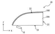
- FIG. 1 is a perspective view illustrating an overall configuration example of a light emitting device 1 according to the first embodiment of the present disclosure.
- FIG. 2A is a plan view illustrating an overall configuration example of the light emitting device 1.
- FIG. 2B is a side view showing a part of the light emitting device 1.
- FIG. 3 is an enlarged perspective view illustrating a configuration example of a main part of the light emitting device 1.
- FIG. 4A is an enlarged cross-sectional view illustrating a configuration example of a main part of the light emitting device 1. Further, FIG.
- FIG. 4B is an explanatory diagram for explaining the path of light from the light source 10 (described later) and the shape of the intermediate light guide 20 (described later).
- the light transmissive material layer 70 (described later) is omitted.
- the light emitting device 1 is used, for example, as a backlight that illuminates a transmissive liquid crystal panel from behind, or as a lighting device in a room or the like.
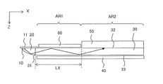
- the light emitting device 1 includes, for example, a plurality of light sources 10, a plurality of intermediate light guides 20, a light guide plate 30, a reflection member 40, and one or a plurality of optical sheets 50.
- the direction in which the optical sheet 50, the light guide plate 30, and the reflection member 40 are arranged is the Z-axis direction (front-rear direction), and the left-right direction (horizontal direction) on the surface 32 that is the widest surface of the light guide plate 30.
- Is the Y-axis direction, and the vertical direction on the surface 32 is the X-axis direction.
- the light emitting device 1 the light emitted from each light source 10 propagates along the X direction through the intermediate light guide 20.
- Each light source 10 is, for example, a light source having a light exit surface on an XY plane.
- Each light source 10 is composed of an LED (Light Emitting Diode).
- Each light source 10 is mounted, for example, on the surface of the substrate 11 arranged in parallel with the XY plane via the solder layer 12, and is arranged in the vicinity of the end face 31 of the light guide plate 30 (see FIGS. 3 and 4A). ).
- the plurality of light sources 10 are provided along the end surface 31 of the light guide plate 30 (see FIG. 2A).
- a reflective layer 13 having a reflective surface 13S is provided on the substrate 11 at a position different from the light source 10 (see FIG. 4A).
- a plurality of intermediate light guides 20 are provided for each light source 10 (see FIG. 2A).
- the plurality of intermediate light guides 20 are provided between each light source 10 and the end face 31 of the light guide plate 30 and are further disposed along the end face 31 of the light guide plate 30 (see FIG. 2A).
- FIG. 3 only one intermediate light guide 20 is shown for easy understanding.
- each intermediate light guide 20 is omitted because each intermediate light guide 20 is hidden behind the substrate 11.
- Each intermediate light guide 20 includes a light transmissive member 20 ⁇ / b> A that covers one corresponding light source 10.
- the light transmissive member 20 ⁇ / b> A is a block-shaped member that propagates light emitted from the covering light source 10 along the X direction.
- the light transmissive member 20A is in contact with the light emitting surface of the light source 10 directly or through an adhesive or the like, and is further in contact with the end surface 31 of the light guide plate 30 through the light transmissive material layer 70 (FIG. 3, see FIG. 4A).
- the light transmissive member 20 ⁇ / b> A is provided in the entire gap between the surface from which each light source 10 emits light and the end surface 31.
- the light transmissive member 20A is formed of a light transmissive material such as a silicone resin. The light transmissive member 20A will be described in detail later.
- the light guide plate 30 guides light from the light source 10 from the end surface 31 to the surface 32.
- the light guide plate 30 mainly includes, for example, a light-transmitting thermoplastic resin such as polycarbonate resin (PC) or acrylic resin (for example, PMMA (polymethyl methacrylate)), or a glass material.
- a light-transmitting thermoplastic resin such as polycarbonate resin (PC) or acrylic resin (for example, PMMA (polymethyl methacrylate)
- PC polycarbonate resin
- acrylic resin for example, PMMA (polymethyl methacrylate)
- the light guide plate 30 includes an end surface 31 on which light emitted from each light source 10 enters via the intermediate light guide unit 20, a surface 32 (upper surface) from which light incident from the end surface 31 is emitted, and its surface 32 is a substantially rectangular parallelepiped light-transmitting member that includes a back surface 33 (lower surface) that faces 32, a side surface 34A that intersects the end surface 31, the front surface 32, and the back surface 33, and that faces in the Y-axis direction.
- the surface 32 extending along the XY plane has, for example, a planar shape corresponding to an irradiation object (for example, a liquid crystal panel 122 described later) disposed to face the surface 32.
- the front surface 32 is preferably parallel to the back surface 33.
- the end surface 31 is preferably perpendicular to the front surface 32 and the back surface 33. Further, as shown in FIG. 4A, a part of the surface 32 may be in contact with the surface of the substrate 11.
- a concave / convex pattern made of fine convex portions is provided in the effective area AR2 of the surface 32 of the light guide plate 30, in order to improve the straightness of light propagating in the light guide plate 30, for example, a concave / convex pattern made of fine convex portions is provided. Good.
- the convex portion is, for example, a strip-shaped ridge or ridge extending in one direction (for example, the vertical direction) of the surface 32.
- a scattering agent may be printed in a pattern on the back surface 33 of the light guide plate 30 as a scattering portion that scatters and makes light propagating through the light guide plate 30 uniform.
- a scattering part it replaces with a scattering agent, and besides providing the site
- the reflection member 40 is a plate-like or sheet-like member provided to face the back surface 33 of the light guide plate 30.
- the reflection member 40 is incident on the light guide plate 30 from the light source 10 via the intermediate light guide unit 20, and then the light leaked from the back surface 33 or transmitted through the back surface 33 from the inside of the light guide plate 30 and emitted.
- the light is returned toward the light guide plate 30.
- the reflection member 40 has functions such as reflection, diffusion, and scattering, for example, so that the light from the light source 10 can be efficiently used and the front luminance can be increased.
- the reflecting member 40 is made of, for example, foamed PET (polyethylene terephthalate), a silver deposited film, a multilayer reflective film, or white PET.
- the surface of the reflecting member 40 is preferably subjected to a treatment such as silver vapor deposition, aluminum vapor deposition, or multilayer film reflection.
- the reflecting member 40 may be integrally formed by a technique such as hot press molding using a thermoplastic resin or melt extrusion molding, or, for example, PET It may be formed by applying an energy ray (for example, ultraviolet ray) curable resin on a substrate made of, for example, and then transferring the shape to the energy ray curable resin.
- the thermoplastic resin include polycarbonate resins, acrylic resins such as PMMA (polymethyl methacrylate resin), polyester resins such as polyethylene terephthalate, and amorphous copolymers such as MS (copolymer of methyl methacrylate and styrene). Examples thereof include a polymerized polyester resin, a polystyrene resin, and a polyvinyl chloride resin.
- the substrate may be glass.
- the one or more optical sheets 50 are provided to face the surface 32 of the light guide plate 30 in the effective area AR2.
- the one or more optical sheets 50 are constituted by, for example, a diffusion plate, a diffusion sheet, a lens film, or a polarization separation sheet. In each figure, only one optical sheet 50 is shown. By providing such an optical sheet 50, light emitted from the light guide plate 30 in an oblique direction can be raised in the front direction, and the front luminance can be further increased.
- the light emitting device 1 further includes a protective member 60 and a light transmissive material layer 70.
- the protective member 60 is provided so as to cover the surface 32 of the light guide plate 30 in the peripheral area AR1 provided between the intermediate light guide 20 and the effective area AR2.
- the protection member 60 is made of, for example, light transmissive resin or glass.
- the peripheral area AR1 is an area in the light guide plate 30 where the optical sheet 50 is not provided.
- the peripheral area AR1 is a light transmissive area that transmits visible light.
- the light transmissive material layer 70 is provided so as to connect the intermediate light guide unit 20 and the light guide plate 30 and is made of a light transmissive adhesive such as ultraviolet (UV) curable resin.
- a light transmissive adhesive such as ultraviolet (UV) curable resin.
- the light transmissive member 20A has a block shape including an upper surface 22, a lower surface 24, a side surface 21A, a side surface 21B, and an opposing surface 23 (see FIG. 3).
- the upper surface 22, the lower surface 24, the side surface 21A, the side surface 21B, and the facing surface 23 constitute an outer surface of the light transmissive member 20A.
- the lower surface 24 is a surface facing the substrate 11 or the reflecting surface 13S.
- the upper surface 22 is a surface facing the lower surface 24.
- the side surface 21A and the side surface 21B are a pair of surfaces facing each other in the Y-axis direction.
- the facing surface 23 is a surface facing the end surface 31 of the light guide plate 30 through the light transmissive material layer 70.
- the light source 10 is surrounded by the reflecting surface 13S, the upper surface 22, the lower surface 24, the side surface 21A, the side surface 21B, and the facing surface 23.
- the light emitted from the light source 10 is directly incident on the facing surface 23, or the reflecting surface 13S, the upper surface 22, the lower surface 24, the side surface 21A and the side surface 21B (hereinafter, these are collectively referred to as “intermediate light guide unit”).
- the light is reflected by at least one of the reflection surfaces 20 and enters the opposing surface 23.
- the light incident on the facing surface 23 passes through the light transmissive material layer 70 and enters the light guide plate 30 from the end surface 31 of the light guide plate 30. Further, it is desirable that the dimension D2 in the Z-axis direction on the facing surface 23 is smaller than the dimension D3 in the Z-axis direction on the end surface 31.
- the upper surface 22 constitutes a part of the outer surface of the light transmissive member 20A.
- the upper surface 22 is a curved interface that reflects light from the light source 10 covered by the light transmissive member 20 ⁇ / b> A and guides the light to the end surface 31 of the light guide plate 30.
- the upper surface 22 is a curved surface that faces the light source 10 and the reflecting surface 13S in the Z-axis direction. Specifically, the upper surface 22 is curved so as to approach parallel to the surface 32 as it approaches the end surface 31 in the X-axis direction and to approach parallel to the end surface 31 as it moves away from the end surface 31.
- the upper surface 22 is substantially parallel to the surface 32 at a position closest to the end surface 31. As shown in FIG. 4A, the distance D1 between the reflecting surface 13S and the front surface 32 in the Z-axis direction is smaller than the distance (thickness D) between the back surface 33 and the front surface 32 in the Z-axis direction. Good.
- the upper surface 22 may include a curved surface portion 22A having a parabolic cross section in the XZ plane and a planar portion 22B continuous with the curved surface portion 22A.
- the curved surface portion 22 ⁇ / b> A may have a focal point F that coincides with the light emitting end P ⁇ b> 1 closest to the end surface 31 of the light source 10. This is because it becomes easier to control the light emitted from the light source 10 to the end face 31.
- the parabola included in the curved surface portion 22A is a quadratic curve drawn at coordinates defined by the symmetry axis J and the axis K orthogonal thereto in the XZ plane.
- the symmetry axis J is preferably inclined by the angle A with respect to the front surface 32 and the back surface 33.
- the angle A is the maximum angle satisfying the total reflection condition in which the light incident on the front surface 32 and the back surface 33 from the inside of the light guide plate 30 is totally reflected without leaking to the outside on the front surface 32 and the back surface 33 (referred to as the maximum light guide angle). ).
- the maximum light guide angle In the light source 10, light emitted from other light emitting points farther from the end face 31 than the light emitting point P1 is incident on the front surface 32 and the back surface 33 at an angle smaller than the angle A, so that the total reflection condition is also satisfied. It is.
- FIG. 4C is an explanatory diagram for explaining the expression (1).
- the upper surface 22 includes only the curved surface portion 22A and does not include the flat surface portion 22B is illustrated.
- the above equations (1) and (2) correspond to the case where the thickness of the light source 10 is sufficiently thin and can be ignored, that is, the case where the light emitting end P1 and the focal point F can be regarded as coincident.
- the thickness d of the light source 10 it is desirable that the position of the light emitting end P1 of the light source 10 be away from the focal point F in the ⁇ X direction by a distance L1 (see FIG. 4D).
- the distance L1 is obtained by Expression (3).
- the light emitting device 1 satisfies the formula (4).
- tanA D / L (4)
- L represents the distance from the light emitting end P1 of the light source 10 to the position where the upper surface 22 is parallel to the surface 32 in the X-axis direction (see FIG. 4E). Further, the expression (4) corresponds to the case where the thickness d of the light source 10 is sufficiently thin and can be ignored.
- Dp 2 ⁇ D ⁇ sinA1 / (1 + sinA1) (6) A ⁇ 0.5 ⁇ A1 ⁇ A ⁇ 1.5 (7) Dp is the distance in the Z-axis direction between the upper surface 22 and the light emitting point P1 at a position corresponding to the position of the light emitting end P1 closest to the end surface 31 in the light source 10.
- A1 is an allowable maximum light guide angle of the upper surface 22 (see FIG. 4E).
- the light emitting device 1 satisfies the following formula (8).
- a ⁇ 90- ⁇ c (8) ⁇ c is a critical angle determined by the refractive index of the light guide plate 30.
- the side surface 21A and the side surface 21B are curved surfaces that stand on the substrate 11 while facing each other with the upper surface 22 and the reflection surface 13S interposed therebetween in the Y-axis direction. Specifically, as shown in FIG. 5A, each of the side surface 21A and the side surface 21B approaches a direction perpendicular to the end surface 31 as it approaches the end surface 31 in the X-axis direction, and approaches a direction parallel to the end surface 31 as it moves away from the end surface 31. Is so curved.
- the side surface 21A and the side surface 21B are substantially perpendicular to both the surface 32 and the end surface 31 at a position closest to the end surface 31.
- the side surface 21A may include a curved surface portion 21A1 having a parabolic cross section in the XY plane and a planar portion 21A2 continuous with the curved surface portion 21A1 (see FIG. 5A).
- the curved surface portion 21A1 may have a focal point F1 on a virtual straight line parallel to the Y axis passing through the light emission point CP at the center of the light source 10.
- the focal point F1 of the curved surface portion 21A1 is preferably located on the curved surface portion 21B1 described later. This is because it becomes easier to control the light emitted from the light source 10 to the end face 31.
- the parabola included in the curved surface portion 21A1 is a quadratic curve drawn at coordinates defined by the symmetry axis S and the axis T orthogonal thereto in the XY plane (see FIG. 5B).
- the symmetry axis S is preferably parallel to the XY plane and inclined by an angle B with respect to the side surfaces 34A and 34B.
- the angle B is the maximum angle (referred to as the maximum light guide angle) that satisfies the total reflection condition in which light incident on the side surfaces 34A and 34B from the inside of the light guide plate 30 is totally reflected without leaking to the outside on the side surfaces 34A and 34B. is there.
- the angle B may coincide with the angle A or may be different.
- the side surface 21B may also have the same configuration as the side surface 21A. That is, as shown in FIG. 5A, the side surface 21B may include a curved surface portion 21B1 having a parabolic cross section in the XY plane and a flat surface portion 21B2 continuous with the curved surface portion 21B1. In that case, the curved surface portion 21 ⁇ / b> B ⁇ b> 1 may have a focal point F ⁇ b> 2 on a virtual straight line parallel to the Y axis passing through the light emission point CP at the center of the light source 10. In particular, the focal point F2 of the curved surface portion 21B1 is preferably located on the curved surface portion 21A1. This is because it becomes easier to control the light emitted from the light source 10 to the end face 31.
- the light emitting device 1 satisfies the following formulas (9) to (11) (see FIG. 5C).
- tanB (W1 + W2) / L2 (9)
- W2 W1 ⁇ sinB1 (10) B1 ⁇ B ⁇ 1.25 (11)
- W1 is the distance in the Y-axis direction from the light emission point CP of the light source 10 to the position where the side surfaces 21A and 21B are perpendicular to the end surface 31.
- W2 is the distance in the Y-axis direction between the light emission point CP of the light source 10 and the side surfaces 21A and 21B.
- L2 is the distance in the X-axis direction from the light emission point CP of the light source 10 to the position where the side surfaces 21A and 21B are perpendicular to the end surface 31.
- B1 is an allowable maximum light guide angle of the side surfaces 21A and 21B.
- the light emitting device 1 satisfies the following formula (12) (see FIG. 5C).
- SX is the dimension of the light source 10 in the X-axis direction.
- SY is a dimension of the light source 10 in the Y-axis direction. W2 ⁇ (SX + SY) / 2 (12)
- the light emitting device 1 satisfies the following formula (13).
- B ⁇ 90- ⁇ c (13) ⁇ c is a critical angle determined by the refractive index of the light guide plate 30.
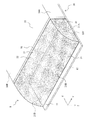
- the intermediate light guide unit 20 includes a reflective layer 20 ⁇ / b> B provided in contact with the upper surface 22, the side surface 21 ⁇ / b> A, and the side surface 21 ⁇ / b> B of the light transmissive member 20 ⁇ / b> A.
- the reflective layer 20B covers the upper surface 22, the side surface 21A, and the side surface 21B of the light transmissive member 20A.
- the reflective layer 20B is made of a dielectric multilayer film in contact with the side surface 21A and the side surface 21B. For example, as illustrated in FIGS.
- the intermediate light guide unit 20 includes a low refractive index layer 20 ⁇ / b> C or a low refractive index layer 20 ⁇ / b> D in contact with the surface of the reflective layer 20 ⁇ / b> B.
- the low refractive index layer 20C is made of air (void) having a refractive index lower than that of the light transmissive member 20A.
- the low refractive index layer 20D is made of a resin having a refractive index lower than that of the light transmissive member 20A.
- the reflectance of the reflective layer 20B is high at a predetermined wavelength and incident angle.
- a high reflectance can be obtained when the incident angle is small.
- FIG. 8 shows the result of using 3M ESR (Enhanced Specular Reflector).
- 3M ESR Enhanced Specular Reflector
- the dielectric multilayer film generally has an optical design that assumes reflection of light incident through the air layer.
- the light is Snell's law. Therefore, the light propagates through the dielectric multilayer film at an angle smaller than the incident angle. Therefore, even if the wavelength region with high reflectivity shifts to the short wavelength side as the incident angle increases, the influence of the shift is slightly mitigated by Snell's law.
- the light from the light source 10 is applied to the reflective layer 20B via the air layer, as shown in the right column of FIGS. 9A, 9B, and 9C, for example. It is not necessarily incident, but is incident on the reflective layer 20B through the light transmissive member 20A made of a material having a refractive index close to that of the reflective layer 20B. Accordingly, the light from the light source 10 is incident on the reflective layer 20B without being refracted so much at the upper surface 22, the side surface 21A, and the side surface 21B. The influence by is great.
- the upper surface of the reflective layer 20B (the back surface of the reflective layer 20B for light propagating in the reflective layer 20B) is in contact with the low refractive index layer 20C or the low refractive index layer 20D. Therefore, for light having a large incident angle, total reflection at the interface between the upper surface of the reflective layer 20B and the low refractive index layer 20C or the low refractive index layer 20D can be used. Thus, in this embodiment, the reflection loss is suppressed by using the total reflection.
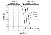
- FIG. 10 shows an example of the wavelength dependence of the reflectance of the reflective layer 20B.
- the reflectance of the reflective layer 20B was measured when light having an incident angle of 30 °, 45 °, 60 °, and 75 ° was incident on the reflective layer 20B. In FIG. 10, the reflection on the upper surface of the reflective layer 20B is not considered.
- the light guide angle in the reflective layer 20B when the incident angle is 30 ° was 19.6 °.
- the incident angle in the reflective layer 20B was 28.3 °.
- the incident angle in the reflective layer 20B was 35.5 °.
- the incident angle in the reflective layer 20B was 40.4 °.
- ESR of 3M company was used.
- the reflectivity of the intermediate light guide 20 when the light guide angle in the reflective layer 20B is 42 °, 45 °, and 50 ° was obtained by prediction.
- FIG. 10 shows that the wavelength at the upper end of the high-reflectance wavelength region gradually decreases as the angle of incidence on the reflective layer 20B increases.
- FIG. 11 shows an example of the incident angle dependence of the reflectance of the reflective layer 20B.
- FIG. 11 shows the results when 3M ESR was used.
- FIG. 11 shows the results when light having wavelengths of 450 nm, 540 nm, and 620 nm is incident on the reflective layer 20B. 42 ° in the figure is a critical angle on the upper surface of the reflective layer 20B when the upper surface of the reflective layer 20B is in contact with the air layer.
- FIG. 11 shows that the angle of the upper end of incident light with high reflectivity gradually decreases as the wavelength of incident light increases.
- the angle of light incident on the upper surface of the reflective layer 20B is 42 ° or more, the light incident on the upper surface of the reflective layer 20B is totally reflected on the upper surface of the reflective layer 20B. Therefore, it can be seen from FIGS. 10 and 11 that the intermediate light guide unit 20 can obtain a high reflectivity at almost all incident angles over almost the entire visible light range.
- the reflective layer 20B preferably has a reflection characteristic according to the refractive index of the low refractive index layer 20D.
- the low refractive index layer 20D is made of a resin having a refractive index of 1.38, and the refractive index of the reflective layer 20B is 1.5.
- the reflective layer 20B preferably has a reflection characteristic of reflecting light having an incident angle to the reflective layer 20B of 67 ° or less.
- the reflective layer 20B preferably has, for example, reflective characteristics having incident angle dependency as shown in Table 1 below. In the reflection characteristics shown in Table 1, light in the visible region is reflected when the incident angle is 67 ° or less.
- the light source 10 is covered with the light transmissive member 20A. For this reason, the light emitted from the light source 10 propagates in the X-axis direction while being reflected by the upper surface 22, the lower surface 24, the side surface 21A and the side surface 21B of the light transmissive member 20A, and the reflecting surface 13S, and from the end surface 31 to the light guide plate 30 is incident.
- part of the light incident on the upper surface 22, side surface 21A, and side surface 21B of the light transmissive member 20A is reflected by the reflective layer 20B provided in contact with the upper surface 22, side surface 21A, and side surface 21B of the light transmissive member 20A. Is done.
- the reflection layer 20B is not provided, the light incident from the light source 10 is less likely to leak to the outside through the upper surface 22, the side surface 21A, or the side surface 21B of the light transmissive member 20A.
- the luminous efficiency can be further improved.
- the low refractive index layer 20C made of air or the low refractive index layer 20D made of resin is provided on the upper surface of the reflective layer 20B.
- the light transmissive member 20A is provided in the entire gap between the surface from which the light from each light source 10 is emitted and the end surface 31. As a result, the number of interfaces that act to scatter the light emitted from each light source 10 can be reduced. As a result, the luminous efficiency can be further improved.
- the upper surface 22, the side surface 21A, and the side surface 21B of the light transmissive member 20A constitute a part of the outer surface of the light transmissive member 20A
- the reflective layer 20B is the light transmissive member 20A.
- the light source 10 is covered by the intermediate light guide 20.
- the light emitted from the light source 10 propagates in the X-axis direction while being reflected on the reflection surface 13S, the upper surface 22, the side surface 21A, and the side surface 21B of the intermediate light guide unit 20, and enters the light guide plate 30 from the end surface 31. It will be. Therefore, for example, compared with the case where the intermediate light guide unit 20 does not include the side surface 21A and the side surface 21B, a component of the light emitted from the light source 10 that leaks outside without entering the light guide plate 30 is reduced.
- the light emission efficiency can be further improved.
- the light emitting device 1 a part of the light rays emitted from each light emitting point of the light source 10 is directly incident on the light guide plate 30 (the end surface 31 thereof). In the XZ plane, the maximum angle of the directly incident light is A.
- filling above-mentioned Formula (8) since the light ray which directly injects into the light-guide plate 30 will satisfy
- the reflecting surface (upper surface 22) can be obtained by matching the light emitting point P1 with the focal point F of the curved surface portion 22A and inclining the symmetry axis J by the angle A. All the light rays reflected by the light incident on the light guide plate 30 (the end face 31) at an angle A. That is, all the light rays emitted from the light emitting end P1 are guided at the angle A.
- the maximum angle of the directly incident light becomes smaller than the angle A.
- a light beam having an angle larger than that of the directly incident light beam is reflected on the reflection surface (upper surface 22).
- the light beam reflected on the reflection surface (upper surface 22) enters the light guide plate 30 at an angle smaller than the angle A as the distance from the focal point F increases. Therefore, the light guide angle of the light emitted from the light emitting end P1 is maximized, and the light is guided at a smaller light guide angle as the distance from the light guide plate 30 increases.
- the light rays from the light emitting end P1 are aligned in the direction close to the X-axis direction, and the light rays emitted from a position farther from the end face 31 than the light emitting end P1 are emitted from the light emitting end P1.
- the light beam travels toward the upper surface 22 at an upward angle closer to the Z-axis direction than the light beam from the light emitting end P ⁇ b> 1, and is reflected on the upper surface 22.
- most of the light rays incident on the light guide plate 30 satisfy the total reflection condition.
- the curved side surfaces 21A and 21B are provided so as to sandwich the light source 10 in the Y-axis direction. Therefore, when the light emitted from the light source 10 is guided in the X-axis direction, the Y-axis The spread in the direction can be controlled. In particular, by setting the light guide angle of the light emitted from the light source 10 to be equal to or less than the angle B, it is possible to avoid the light from leaking from the side surfaces 34A and 34B of the light guide plate 30.
- the peripheral area AR1 is provided between the end face 31 and the effective area AR2, the lights emitted from the plurality of light sources 10 arranged in the Y-axis direction are mixed, and the Y-axis direction is mixed. It is possible to emit light having a more uniform intensity distribution in FIG. 5, that is, light with reduced luminance unevenness, from the surface 32 in the effective area AR2.
- the luminance unevenness at the stage of reaching the effective area AR2 is determined by the maximum light guide angle B in the XY plane and the distance LX from the end surface 31 of the light guide plate 30 to the effective area AR2. Therefore, by providing the peripheral area AR1 between the end face 31 and the effective area AR2, it is possible to reduce luminance unevenness without increasing the maximum light guide angle B.
- the maximum light guide angle B can be reduced by increasing the dimension in the X-axis direction of the peripheral area AR1 and increasing the distance LX from the end face 31 to the effective area AR2. That is, the number of the light sources 10 arranged in the Y-axis direction can be reduced, and the interval between the adjacent light sources 10 in the Y-axis direction can be increased.
- the light emitting device 1 is mounted on a device such as a display device, for example, by providing the peripheral region AR1, the light source 10 serving as a heat source can be moved away from the effective region AR2 that overlaps the display panel, for example. Therefore, in this case, the long-term reliability of the display device equipped with the light emitting device 1 can be improved.
- the effect which improves the designability by exposing a part of light-guide plate 30 positively and showing it to a user can also be anticipated.
- the light beam incident on the light guide plate 30 propagates at the maximum light guide angle (angle A and angle B) that satisfies the total reflection condition, and therefore does not leak from the surface 32 in the peripheral area AR1.
- angle A and angle B the maximum light guide angle that satisfies the total reflection condition
- the angle A and the angle B are sufficiently smaller than a value (90 ⁇ c) defined by the critical angle ⁇ c of the light guide plate 30 to have a margin.
- a transparent protective member 60 may be provided so as to cover the surface 32 in the peripheral area AR1 for the purpose of protecting the surface 32 from foreign matter adhesion and scratches during use.
- the substrates are arranged on the back surface of the effective screen. This is because the frame width is desired to be narrow in terms of design.
- the overall thickness can be reduced by arranging the substrates on the same plane as the front surface 32 without arranging the substrates on the side facing the back surface 33. For example, when installed on a wall surface, the back wall surface can be seen through the transparent peripheral area AR1, so that the feeling of pressure is small and the design is excellent.
- the distance D1 between the reflecting surface 13S and the front surface 32 is smaller than the distance (thickness D) between the back surface 33 and the front surface 32, and the Z-axis direction of the opposing surface 23
- the dimension D2 of the light source 10 is smaller than the dimension D3 of the end surface 31 in the Z-axis direction, and the block 14 is provided. Therefore, when light emitted from the light source 10 enters the light guide plate 30 from the intermediate light guide unit 20, Can be prevented from leaking.
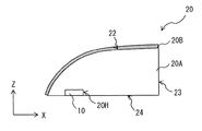
- FIG. 14 illustrates a state in which an area facing the light source 10 in the inner surface of the recess 20H is a curved surface.
- FIG. 14 further illustrates a state in which the lens member 10 ⁇ / b> A is provided on the light emitting surface of the light source 10.
- FIG. 15 illustrates a state in which the light transmissive member 20A is greatly swollen and the inner surface of the recess 20H follows the outer surface of the light transmissive member 20A. Even if the light transmissive member 20A is in the form shown in FIGS. 13 to 15, it is possible to obtain an effect close to the effect in the above embodiment.
- the lower surface 24 of the light transmissive member 20A is provided with the depression 20H as shown in FIG. 12, for example.
- the lower surface 24 of the light transmissive member 20 ⁇ / b> A may be a flat surface.
- the light source 10 may be disposed such that the light emission surface of the light source 10 is in contact with the lower surface 24 of the light transmissive member 20 ⁇ / b> A. Further, for example, as illustrated in FIG.
- the light source 10 may be arranged such that an air layer (gap) exists between the light emitting surface of the light source 10 and the lower surface 24 of the light transmissive member 20 ⁇ / b> A. Good. Even when the light transmissive member 20 ⁇ / b> A is in the form described in FIGS. 16 and 17, an effect close to the effect in the above embodiment can be obtained.
- the light source 10 is provided so that the light emitting surface of the light source 10 and the substrate 11 are parallel to each other.
- the light source 10 is provided such that the light emitting surface of the light source 10 and the substrate 11 are not parallel to each other. May be.
- the light source 10 may be disposed inside the recess 20H, for example, as shown in FIG. Further, for example, as illustrated in FIG. 19, the light source 10 may be arranged such that an air layer (gap) exists between the light emitting surface of the light source 10 and the flat lower surface 24.
- the reflective layer 20B is provided in contact with all of the upper surface 22, the side surface 21A, and the side surface 21B of the light transmissive member 20A.
- the reflective layer 20B may be provided in contact with at least a part of the upper surface 22, the side surface 21A, and the side surface 21B of the light transmissive member 20A.
- the reflective layer 20B may be provided in contact with only the upper surface 22 of the light transmissive member 20A. Even when the reflective layer 20B is in the form shown in FIG. 20, it is possible to obtain an effect close to the effect in the above embodiment.
- the plurality of intermediate light guides 20 are assigned to each light source 10 one by one.
- one intermediate light guide 20 ⁇ / b> Y may be provided instead of the plurality of intermediate light guides 20.
- the intermediate light guide unit 20Y is provided between each light source 10 and the end surface 31 of the light guide plate 30, and further, the long side of the intermediate light guide unit 20Y is disposed along the end surface 31 of the light guide plate 30. Yes.
- the intermediate light guide 20Y is assigned to all the light sources 10 in common.
- the intermediate light guide 20Y includes a light transmissive member 20Y1 that covers all the light sources 10.
- the light transmissive member 20Y1 is a block-like member that propagates most of the light emitted from all the covered light sources 10 along the X direction.
- the light transmissive member 20Y1 is in contact with the light emission surface of the light source 10 directly or through an adhesive or the like, and is further in contact with the end surface 31 of the light guide plate 30 through the light transmissive material layer 70.
- the light transmissive member 20 ⁇ / b> Y ⁇ b> 1 is provided in the entire gap between the surface from which each light source 10 emits light and the end surface 31.
- the light transmissive member 20Y1 is made of a light transmissive material such as silicone resin.
- the light transmissive member 20Y1 has a block shape including the upper surface 22, the lower surface 24, the side surface 21A, the side surface 21B, and the facing surface 23, similarly to the light transmissive member 20A.
- the upper surface 22, the lower surface 24, the side surface 21A, the side surface 21B, and the facing surface 23 constitute an outer surface of the light transmissive member 20Y1.
- the light transmissive member 20Y1 may have, for example, one recess 20H described in FIGS. 12 to 15 and FIG.
- the light transmissive member 20Y1 may have a flat lower surface 24 described in FIGS. 16, 17, and 19, for example. At this time, each light source 10 may be arranged as shown in FIGS. 16, 17, and 19, for example.
- the reflective layer 20B is provided in contact with all of the upper surface 22, the side surface 21A, and the side surface 21B of the light transmissive member 20Y1. Therefore, an effect equivalent to the effect in the above embodiment can be obtained.
- the plurality of light sources 10 may be arranged in a line along the side surface 31 of the light guide plate 30.
- the arrangement pitch of the plurality of light sources 10 may be equal.
- the pitch may be non-uniform.
- the distance between each light source 10 and the end surface 31 of the light guide plate 30 may be uniform or non-uniform.
- the plurality of light sources 10 may be arranged in a plurality of rows along the side surface 31 of the light guide plate 30.
- the reflective layer 20B may be provided in contact with at least a part of the upper surface 22, the side surface 21A, and the side surface 21B of the light transmissive member 20Y1.
- the reflective layer 20B may be provided in contact with only the upper surface 22 of the light transmissive member 20Y1. Even when the reflective layer 20B is in the form shown in FIG. 22, it is possible to obtain an effect close to the effect of the modification E.
- FIG. 23 illustrates an appearance of the display device 101 according to the second embodiment of the present disclosure.
- the display device 101 includes the light emitting device 1 and is used as, for example, a thin television device.
- the display device 101 has a configuration in which a flat main body 102 for image display is supported by a stand 103.
- the display device 101 is used as a stationary type with the stand 103 attached to the main body 102 and placed on a horizontal surface such as a floor, a shelf, or a stand, but the stand 103 is removed from the main body 102. It can also be used as a wall-hanging type.
- FIG. 24 is an exploded view of the main body 102 shown in FIG.
- the main body 102 has, for example, a front exterior member (bezel) 111, a panel module 112, and a rear exterior member (rear cover) 113 in this order from the front side (viewer side).
- the front exterior member 111 is a frame-shaped member that covers the peripheral edge of the front surface of the panel module 112, and a pair of speakers 114 are disposed below the front exterior member 111.
- the panel module 112 is fixed to the front exterior member 111, and a power supply board 115 and a signal board 116 are mounted on the rear surface thereof, and a mounting bracket 117 is fixed.
- the mounting bracket 117 is for mounting a wall-mounted bracket, mounting a board, etc., and mounting the stand 103.
- the rear exterior member 113 covers the back and side surfaces of the panel module 112.
- FIG. 25 is an exploded view of the panel module 112 shown in FIG.
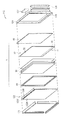
- the panel module 112 includes, for example, a front casing (top chassis) 121, a liquid crystal panel 122, a frame member (middle chassis) 80, an optical sheet 50, and a light guide plate 30 from the front side (viewer side).
- the light source 10, the reflection member 40, the rear housing (back chassis) 124, and the timing controller board 127 are provided in this order.
- the front housing 121 is a frame-shaped metal part that covers the front peripheral edge of the liquid crystal panel 122.
- the liquid crystal panel 122 includes, for example, a liquid crystal cell 122A, a source substrate 122B, and a flexible substrate 122C such as a COF (Chip On On Film) that connects them.
- the frame-shaped member 123 is a frame-shaped resin component that holds the liquid crystal panel 122 and the optical sheet 50.
- the rear housing 124 is a metal part made of iron (Fe) or the like that houses the liquid crystal panel 122, the intermediate housing 123, and the light emitting device 1.
- the timing controller board 127 is also mounted on the back surface of the rear housing 124.
- the display device 101 In the display device 101, light from the light emitting device 1 is selectively transmitted through the liquid crystal panel 122, thereby displaying an image.
- the display quality of the display device 101 is improved.
- display device 101 As described above to an electronic device will be described.
- the electronic device include a television device, a digital camera, a notebook personal computer, a mobile terminal device such as a mobile phone, or a video camera.
- the display device can be applied to electronic devices in various fields that display a video signal input from the outside or a video signal generated inside as an image or video.
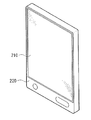
- FIG. 26 shows an appearance of a tablet terminal device to which the display device 101 of the above embodiment is applied.
- FIG. 27 illustrates an appearance of another tablet terminal device to which the display device 101 according to the above-described embodiment is applied.
- Each of these tablet-type terminal devices has, for example, a display unit 210 and a non-display unit 220, and the display unit 210 is configured by the display device 101 of the above embodiment.
- FIG. 28 and FIG. 29 show the external appearance of a tabletop or floor-standing lighting device to which the light-emitting device 1 of the above embodiment is applied.
- a lighting unit 843 is attached to a support column 842 provided on a base 841.
- the illumination unit 843 is configured by the light emitting device 1.
- the illumination unit 843 can have an arbitrary shape such as a cylindrical shape shown in FIG. 28 or a curved shape shown in FIG. 29 by making the light guide plate 20 into a curved shape.
- FIG. 30 shows an appearance of an indoor lighting device to which the light emitting device 1 is applied.
- This illuminating device has the illumination part 844 comprised by the said light-emitting device 1, for example.
- the illumination units 844 are arranged at an appropriate number and interval on the ceiling 850A of the building. Note that the lighting unit 844 can be installed not only in the ceiling 850A but also in an arbitrary place such as a wall 850B or a floor (not shown) depending on the application.
- illumination is performed by light from the light emitting device 1.
- the light emitting device 1 having high luminous efficiency is used, the illumination quality is improved.
- this indication can take the following composition.
- a light guide plate having an end surface, an upper surface, and a lower surface; A plurality of light sources provided along the end surface; One or a plurality of light transmissive members provided between each of the light sources and the end surface, and having a curved interface that reflects light from each of the light sources and guides the light to the end surface; A reflective layer made of a dielectric multilayer film provided in contact with the interface; And a low refractive index layer having a refractive index lower than that of the light transmissive member, which is provided in contact with the reflective layer.
- the low refractive index layer is made of air or resin.
- a light emitting device for emitting illumination light A display panel that is arranged so as to overlap with the light emitting device and displays an image using the illumination light, and The light emitting device
- a light guide plate having an end surface, an upper surface including an emission region from which the illumination light is emitted, and a lower surface;
- a plurality of light sources provided along the end surface;
- One or a plurality of light transmissive members provided between each of the light sources and the end surface, and having a curved interface that reflects light from each of the light sources and guides the light to the end surface;
- a reflective layer made of a dielectric multilayer film provided in contact with the interface;
- a display device comprising: a low refractive index layer provided in contact with the reflective layer and having a refractive index lower than that of the light transmissive member.
- a light emitting device for emitting illumination light The light emitting device A light guide plate having an end surface, an upper surface including an emission region from which the illumination light is emitted, and a lower surface; A plurality of light sources provided along the end surface; One or a plurality of light transmissive members provided between each of the light sources and the end surface, and having a curved interface that reflects light from each of the light sources and guides the light to the end surface; A reflective layer made of a dielectric multilayer film provided in contact with the interface; And a low refractive index layer having a refractive index lower than that of the light transmissive member provided in contact with the reflective layer.
Abstract
Selon un mode de réalisation, la présente invention concerne un dispositif électroluminescent qui comporte une plaque de guide de lumière, une pluralité de sources de lumière le long de la face d'extrémité de la plaque de guide de lumière, et un organe ou une pluralité d'organes transparents à la lumière placés entre les sources de lumière et la face d'extrémité de la plaque de guide de lumière. L'organe ou la pluralité d'organes transparents à la lumière comportent des faces limites incurvées qui réfléchissent la lumière des sources de lumière et qui guident la lumière vers la face d'extrémité. Ce dispositif électroluminescent comporte en outre une couche réfléchissante qui est placée en contact avec les faces limites et qui comprend une pellicule diélectrique multicouche, et une couche à faible indice de réfraction qui est placée en contact avec la couche réfléchissante et dont l'indice de réfraction est inférieur à celui des organes transparents à la lumière.
Applications Claiming Priority (2)
| Application Number | Priority Date | Filing Date | Title |
|---|---|---|---|
| JP2016060382 | 2016-03-24 | ||
| JP2016-060382 | 2016-03-24 |
Publications (1)
| Publication Number | Publication Date |
|---|---|
| WO2017163608A1 true WO2017163608A1 (fr) | 2017-09-28 |
Family
ID=59901111
Family Applications (1)
| Application Number | Title | Priority Date | Filing Date |
|---|---|---|---|
| PCT/JP2017/003108 WO2017163608A1 (fr) | 2016-03-24 | 2017-01-30 | Dispositif électroluminescent, dispositif d'affichage, et dispositif d'éclairage |
Country Status (1)
| Country | Link |
|---|---|
| WO (1) | WO2017163608A1 (fr) |
Cited By (4)
| Publication number | Priority date | Publication date | Assignee | Title |
|---|---|---|---|---|
| CN112764150A (zh) * | 2019-10-21 | 2021-05-07 | 元太科技工业股份有限公司 | 前光模块及显示装置 |
| JP2021106159A (ja) * | 2019-07-01 | 2021-07-26 | 大日本印刷株式会社 | 拡散部材、積層体、拡散部材のセット、ledバックライトおよび表示装置 |
| JP2021106137A (ja) * | 2019-12-27 | 2021-07-26 | 日亜化学工業株式会社 | 線状光源の製造方法 |
| CN115079466A (zh) * | 2021-03-12 | 2022-09-20 | 南京瀚宇彩欣科技有限责任公司 | 导光模组 |
Citations (6)
| Publication number | Priority date | Publication date | Assignee | Title |
|---|---|---|---|---|
| JP2000155315A (ja) * | 1998-09-14 | 2000-06-06 | Sharp Corp | フロントライト及び反射型液晶表示装置 |
| JP2004199967A (ja) * | 2002-12-18 | 2004-07-15 | Advanced Display Inc | 面状光源装置、液晶表示装置及び表示装置 |
| JP2007234385A (ja) * | 2006-02-28 | 2007-09-13 | Yamaha Corp | バックライト装置 |
| JP2007317659A (ja) * | 2006-05-26 | 2007-12-06 | Avago Technologies General Ip (Singapore) Private Ltd | 光導波路を照明するための間接照明装置 |
| JP2009506503A (ja) * | 2005-08-27 | 2009-02-12 | スリーエム イノベイティブ プロパティズ カンパニー | 凹面トランスフレクターを備えた光リサイクリングキャビティーを有する端部照明バックライト |
| JP2013218953A (ja) * | 2012-04-11 | 2013-10-24 | Sony Corp | 発光装置、表示装置および照明装置 |
-
2017
- 2017-01-30 WO PCT/JP2017/003108 patent/WO2017163608A1/fr active Application Filing
Patent Citations (6)
| Publication number | Priority date | Publication date | Assignee | Title |
|---|---|---|---|---|
| JP2000155315A (ja) * | 1998-09-14 | 2000-06-06 | Sharp Corp | フロントライト及び反射型液晶表示装置 |
| JP2004199967A (ja) * | 2002-12-18 | 2004-07-15 | Advanced Display Inc | 面状光源装置、液晶表示装置及び表示装置 |
| JP2009506503A (ja) * | 2005-08-27 | 2009-02-12 | スリーエム イノベイティブ プロパティズ カンパニー | 凹面トランスフレクターを備えた光リサイクリングキャビティーを有する端部照明バックライト |
| JP2007234385A (ja) * | 2006-02-28 | 2007-09-13 | Yamaha Corp | バックライト装置 |
| JP2007317659A (ja) * | 2006-05-26 | 2007-12-06 | Avago Technologies General Ip (Singapore) Private Ltd | 光導波路を照明するための間接照明装置 |
| JP2013218953A (ja) * | 2012-04-11 | 2013-10-24 | Sony Corp | 発光装置、表示装置および照明装置 |
Cited By (10)
| Publication number | Priority date | Publication date | Assignee | Title |
|---|---|---|---|---|
| JP2021106159A (ja) * | 2019-07-01 | 2021-07-26 | 大日本印刷株式会社 | 拡散部材、積層体、拡散部材のセット、ledバックライトおよび表示装置 |
| JP7044186B2 (ja) | 2019-07-01 | 2022-03-30 | 大日本印刷株式会社 | 拡散部材、積層体、拡散部材のセット、ledバックライトおよび表示装置 |
| JP2022071213A (ja) * | 2019-07-01 | 2022-05-13 | 大日本印刷株式会社 | 拡散部材、積層体、拡散部材のセット、ledバックライトおよび表示装置 |
| JP7103541B2 (ja) | 2019-07-01 | 2022-07-20 | 大日本印刷株式会社 | 拡散部材、積層体、拡散部材のセット、ledバックライトおよび表示装置 |
| JP2022141711A (ja) * | 2019-07-01 | 2022-09-29 | 大日本印刷株式会社 | 拡散部材、積層体、拡散部材のセット、ledバックライトおよび表示装置 |
| CN112764150A (zh) * | 2019-10-21 | 2021-05-07 | 元太科技工业股份有限公司 | 前光模块及显示装置 |
| JP2021106137A (ja) * | 2019-12-27 | 2021-07-26 | 日亜化学工業株式会社 | 線状光源の製造方法 |
| JP7121298B2 (ja) | 2019-12-27 | 2022-08-18 | 日亜化学工業株式会社 | 線状光源の製造方法 |
| US11757063B2 (en) | 2019-12-27 | 2023-09-12 | Nichia Corporation | Method for manufacturing linear light source |
| CN115079466A (zh) * | 2021-03-12 | 2022-09-20 | 南京瀚宇彩欣科技有限责任公司 | 导光模组 |
Similar Documents
| Publication | Publication Date | Title |
|---|---|---|
| US9523808B2 (en) | Thin film type back light unit for flat panel display | |
| CN105425334B (zh) | 显示设备 | |
| US9638956B2 (en) | Backlight unit and display apparatus thereof | |
| US10302837B2 (en) | Backlight unit and liquid crystal display including the same | |
| JP6991373B2 (ja) | 発光装置、表示装置および照明装置 | |
| CN107884998B (zh) | 背光模组及具有该背光模组的显示装置 | |
| US10317610B2 (en) | Illumination device and display device | |
| WO2017163608A1 (fr) | Dispositif électroluminescent, dispositif d'affichage, et dispositif d'éclairage | |
| TWI626482B (zh) | 可切換視角的背光單元 | |
| JP7166413B2 (ja) | 発光装置、表示装置および照明装置 | |
| US10620361B2 (en) | Super directional light guide film and thin film type back light unit for flat panel display using the same | |
| JP4645314B2 (ja) | 導光板とそれを用いたエッジライト型面光源および液晶表示装置 | |
| KR20040075725A (ko) | 도광판의 양면으로부터 광을 출사하게 하는 데에 적합한확산 조명장치 | |
| EP3605214A1 (fr) | Dispositif d'affichage | |
| WO2016147505A1 (fr) | Dispositif d'allumage, dispositif d'affichage, et dispositif d'éclairage | |
| US10788703B2 (en) | Frame, surface light source device, display device and electronic device | |
| KR20140067471A (ko) | 확산용 도광필름, 백라이트부 및 이를 구비한 액정표시소자 | |
| US20220004059A1 (en) | Display And Electronic Apparatus | |
| TWI275871B (en) | Backlight system | |
| CN114141164A (zh) | 电子设备 | |
| JP6708593B2 (ja) | 表示装置 | |
| CN216434597U (zh) | 背光模组、显示装置及电子设备 | |
| WO2017169047A1 (fr) | Dispositif émetteur de lumière, dispositif d'affichage et dispositif d'éclairage | |
| WO2017073175A1 (fr) | Dispositif électroluminescent, appareil d'affichage et appareil d'éclairage | |
| TWI359289B (en) | Optical plate and backlight module using the same |
Legal Events
| Date | Code | Title | Description |
|---|---|---|---|
| NENP | Non-entry into the national phase |
Ref country code: DE |
|
| 121 | Ep: the epo has been informed by wipo that ep was designated in this application |
Ref document number: 17769655 Country of ref document: EP Kind code of ref document: A1 |
|
| 122 | Ep: pct application non-entry in european phase |
Ref document number: 17769655 Country of ref document: EP Kind code of ref document: A1 |
|
| NENP | Non-entry into the national phase |
Ref country code: JP |