WO2017159793A1 - コネクタ - Google Patents
コネクタ Download PDFInfo
- Publication number
- WO2017159793A1 WO2017159793A1 PCT/JP2017/010693 JP2017010693W WO2017159793A1 WO 2017159793 A1 WO2017159793 A1 WO 2017159793A1 JP 2017010693 W JP2017010693 W JP 2017010693W WO 2017159793 A1 WO2017159793 A1 WO 2017159793A1
- Authority
- WO
- WIPO (PCT)
- Prior art keywords
- terminal group
- terminal
- housing
- connector
- protrusion
- Prior art date
- Legal status (The legal status is an assumption and is not a legal conclusion. Google has not performed a legal analysis and makes no representation as to the accuracy of the status listed.)
- Ceased
Links
Images




Classifications
-
- H—ELECTRICITY
- H01—ELECTRIC ELEMENTS
- H01R—ELECTRICALLY-CONDUCTIVE CONNECTIONS; STRUCTURAL ASSOCIATIONS OF A PLURALITY OF MUTUALLY-INSULATED ELECTRICAL CONNECTING ELEMENTS; COUPLING DEVICES; CURRENT COLLECTORS
- H01R12/00—Structural associations of a plurality of mutually-insulated electrical connecting elements, specially adapted for printed circuits, e.g. printed circuit boards [PCB], flat or ribbon cables, or like generally planar structures, e.g. terminal strips, terminal blocks; Coupling devices specially adapted for printed circuits, flat or ribbon cables, or like generally planar structures; Terminals specially adapted for contact with, or insertion into, printed circuits, flat or ribbon cables, or like generally planar structures
- H01R12/70—Coupling devices
- H01R12/71—Coupling devices for rigid printing circuits or like structures
-
- H—ELECTRICITY
- H01—ELECTRIC ELEMENTS
- H01R—ELECTRICALLY-CONDUCTIVE CONNECTIONS; STRUCTURAL ASSOCIATIONS OF A PLURALITY OF MUTUALLY-INSULATED ELECTRICAL CONNECTING ELEMENTS; COUPLING DEVICES; CURRENT COLLECTORS
- H01R13/00—Details of coupling devices of the kinds covered by groups H01R12/70 or H01R24/00 - H01R33/00
- H01R13/646—Details of coupling devices of the kinds covered by groups H01R12/70 or H01R24/00 - H01R33/00 specially adapted for high-frequency, e.g. structures providing an impedance match or phase match
- H01R13/6461—Means for preventing cross-talk
-
- H—ELECTRICITY
- H01—ELECTRIC ELEMENTS
- H01R—ELECTRICALLY-CONDUCTIVE CONNECTIONS; STRUCTURAL ASSOCIATIONS OF A PLURALITY OF MUTUALLY-INSULATED ELECTRICAL CONNECTING ELEMENTS; COUPLING DEVICES; CURRENT COLLECTORS
- H01R13/00—Details of coupling devices of the kinds covered by groups H01R12/70 or H01R24/00 - H01R33/00
- H01R13/648—Protective earth or shield arrangements on coupling devices, e.g. anti-static shielding
- H01R13/658—High frequency shielding arrangements, e.g. against EMI [Electro-Magnetic Interference] or EMP [Electro-Magnetic Pulse]
- H01R13/6581—Shield structure
- H01R13/6585—Shielding material individually surrounding or interposed between mutually spaced contacts
-
- H—ELECTRICITY
- H01—ELECTRIC ELEMENTS
- H01R—ELECTRICALLY-CONDUCTIVE CONNECTIONS; STRUCTURAL ASSOCIATIONS OF A PLURALITY OF MUTUALLY-INSULATED ELECTRICAL CONNECTING ELEMENTS; COUPLING DEVICES; CURRENT COLLECTORS
- H01R24/00—Two-part coupling devices, or either of their cooperating parts, characterised by their overall structure
- H01R24/60—Contacts spaced along planar side wall transverse to longitudinal axis of engagement
Definitions
- the present invention relates to a connector suitable for high-speed transmission of electrical signals. Specifically, when a plurality of terminals included in the connector are arranged close to each other, a structure in an insulating housing capable of preventing the occurrence of crosstalk between the terminals due to mutual capacitance or induction. About.
- a connector used for transmitting an electrical signal or the like generally includes an insulating housing that holds one terminal group and the other terminal group facing each other, and an outer conductor shell that houses the housing.
- an insulating housing that holds one terminal group and the other terminal group facing each other
- an outer conductor shell that houses the housing.
- one terminal group and the other are Some have a plate-like conductive member between the terminals.
- a connector described in Japanese Patent Application Laid-Open No. 2015-179591 includes a plurality of terminals arranged at intervals from each other, one terminal group arranged at the upper part and the terminal group arranged at the lower part. A plurality of terminals arranged so that the other terminal group faces each other, an insulating holding member (housing) holding each terminal, and a metal shell (external conductor shell) covering the housing holding each terminal And a ground member formed by punching a single metal plate between one terminal group and the other terminal group.
- a conventional connector having an insulating housing that holds one terminal group and the other terminal group facing each other includes a plurality of terminals included in each terminal group.
- two terminal groups arranged so as to face each other along the fitting direction of the connector, an insulating housing that holds the terminal groups, and an external housing the housing
- the housing In the board-side connector including the conductor shell, the housing is divided into a first housing member that holds the first terminal group and a second housing member that holds the second terminal group.
- An accommodating portion for accommodating the conductive plate is provided on at least one of the side surfaces (that is, the side surface on the central axis side in the fitting direction of the connector, hereinafter referred to as “mating surface”) facing each other.
- a first terminal group and the second terminal group is electrically disconnected, it is possible to suppress the occurrence of crosstalk, to provide a connector capable of electrically adversely reduce or avoid to high-frequency characteristics.
- a connector includes: A connector including at least a terminal group including a first terminal group and a second terminal group disposed so as to face each other along a fitting direction of the connector, and an insulating housing holding the terminal group.
- the housing includes a first housing member that holds the first terminal group, and a second housing member that holds the second terminal group, A conductive member is included between the first housing member and the second housing member.
- the terminal group includes a vertical portion in which a plurality of terminals are arranged in a direction perpendicular to a board on which the connector is mounted,
- the conductive member is sandwiched between the first housing member and the second housing member between the vertical portion of the first terminal group and the vertical portion of the second terminal group. It is characterized by.
- An accommodation portion for accommodating the conductive member is provided on at least one of the surfaces.
- the conductive member is composed of a plurality of partially conductive members.
- the first terminal group and the second terminal group each have a contact portion and a terminal mounting portion, and the arrangement direction and terminals of the contact portions in the first terminal group and the second terminal group
- the mounting parts are arranged so that their arrangement directions are orthogonal to each other.
- the conductive member has a shape that blocks between the vertical portion of the first terminal group and the vertical portion of the second terminal group.
- Each of the first terminal group and the second terminal group includes at least one terminal pair including two terminals.
- the first terminal group and the second terminal group include two or more sets of the terminal pairs and one or more ground terminals, The ground terminal is disposed between each of the terminal pairs.
- the conductive member is electrically connected to at least one of a ground terminal included in the first terminal group and a ground terminal included in the second terminal group.
- the connector further includes an outer conductor shell for housing the housing.
- the conductive member is electrically connected to the outer conductor shell.
- the conductive member includes a mounting part for mounting on a substrate.
- the connector according to the present invention divides a housing holding two terminal groups into a first housing member holding the first terminal group and a second housing member holding the second terminal group, By electrically shielding a conductive plate between a part of each terminal included in the first terminal group and a part of each terminal included in the second terminal group arranged in the vertical direction.
- the occurrence of crosstalk between the first terminal group and the second terminal group can be suppressed, and adverse electrical effects on the high frequency characteristics can be reduced or avoided.
- FIG. 1 is a diagram showing the appearance of a board-side connector and a cable-side connector.
- the connector fitting direction is the X1-X2 direction (X-axis direction) in the figure.
- the tip side of the board-side connector 100 is the X2 direction side
- the tip side of the cable-side connector 200 is the X1 direction side.
- a plane perpendicular to the substrate 300 is an XZ plane
- a plane (parallel plane) to the substrate 300 is an XY plane.
- the upper and lower sides along the Z-axis direction in the figure are the upper and lower sides of each connector. The above matters are the same in other drawings.
- the board-side connector 100 is a housing 150 molded of an insulating material such as a synthetic resin that holds a plurality of terminals that form the fitting protrusions 104 on the connection side (X2 direction side) with the cable-side connector 200. (See FIG. 3A or 3B) and an outer conductor shell 106 including a housing 150 therein.
- the outer conductor shell 106 includes shell mounting portions 108 a and 108 b for mounting and fixing the outer conductor shell 106 to the substrate 300.
- the shell mounting portions 108a and 108b are dip terminals that are inserted into holes provided in the substrate 300 and soldered, but may be terminals that can be mounted on the surface of the substrate.
- the shell mounting portion 108a is provided on the side surface on the distal end side (X2 side) of the connector 100 with respect to the shell mounting portion 108b.
- the outer conductor shell 106 includes a lock hole 110 that engages with the lock protrusion 206 of the connector 200 on the cable side.
- the lock hole 110 is provided at a position where it can engage with the lock projection 206 of the connector 200 on the cable side.
- the lock holes 110 are provided on the upper and lower (upper and lower sides in the Z-axis direction) side walls of the outer conductor shell 106 of the connector 100.
- the lock hole 110 may not necessarily be a hole penetrating the outer conductor shell as long as it can be engaged with the lock protrusion 206.
- a lock protrusion may be provided in the outer conductor shell of the connector on the board side, and a lock hole may be provided in the outer conductor shell of the connector on the cable side.
- the rear wall portion 112 is provided on the rear side (X1 side) of the outer conductor shell 106 and has a shell mounting portion 114 at the tip portion.
- the shell mounting portion 114 is formed integrally with the rear wall portion 112 of the outer conductor shell 106, and is provided on the rear end side of the outer conductor shell 106 along the rear wall (X1 side wall) of the housing 150. It also serves as a shell mounting portion, and is mounted on the substrate 300 through a space between two terminal groups (terminal mounting portions 132a and 132b) exposed from the housing 150.
- the shell mounting portion 114 serves as a ground electrode for a plurality of terminals included in the two terminal groups, even in an embodiment in which a ground terminal is not provided between each of the plurality of terminals transmitting signals, the electrical signal High frequency characteristics necessary for high-speed transmission can be maintained.
- the number of terminals included in the connector can be reduced, and by reducing the number of terminals (ie, the number of parts), the internal structure of the connector is simplified and the impedance matching can be easily adjusted. Can be.
- the housing 150 accommodated in the outer conductor shell 106 has two terminal groups arranged so as to face each other along the fitting direction of the connector 100 (FIG. 5A). (See (b)), and a plurality of terminals included in the two terminal groups are exposed from the housing 150 at the rear (X1 side) of the external conductor shell 106 and are provided on the exposed terminals.
- 132 (132a, 132b) is soldered and fixed onto the surface of the substrate 300.
- Each terminal mounting portion 132 is surface-mounted on the substrate 300, but may be configured as a dip terminal so as to be mounted by being inserted into a hole provided in the substrate.
- the cable-side connector 200 has a fitting portion 202 on the connection side (X1 direction side) to the board-side connector 100, an external conductor shell 204 in which a housing holding a plurality of terminals is housed, and an external conductor
- the lock operation button 208 interlocks with the lock protrusion 206 protruding from the hole of the shell 204, and the cover member 210 that covers the connection portion between the outer conductor shell 204 and the cable 400.
- the fitting portion 202 is inserted into the fitting recess 102 (see FIG. 2 (a) or (b)) when connected to the connector 100 on the board side.
- the outer conductor shell 204 has a hole in the side wall for projecting the lock projection 206 from the inside.
- the lock protrusion 206 is provided at a position where it can engage with the lock hole 110 of the connector 100 on the board side.
- the lock protrusion 206 is provided on the upper and lower (upper and lower sides in the Z-axis direction) side walls of the outer conductor shell 204 of the connector 200.
- the lock protrusion 206 may have any structure as long as it can engage with the lock hole 110.
- the lock protrusion 206 is connected to the lock operation button 208 inside the outer conductor shell 204, and the lock protrusion 206 is pushed in in conjunction with the depression of the lock operation button 208.
- the lock operation button 208 is pushed in when connected to the board-side connector 100, the lock projection 206 is removed from the lock hole 110, and the cable-side connector 200 can be pulled out of the board-side connector 100.
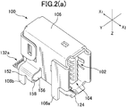
- FIGS. 2A and 2B are views showing the appearance of a board-side connector (hereinafter simply referred to as “connector”) according to an embodiment of the present invention.
- FIG. 2A is a perspective view of the connector 100 as viewed from the upper end side (X2 side)
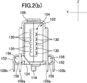
- FIG. 2B is a front view of the connector 100 as viewed from the side surface (X2 side).
- the housing 150 see FIG. 3 (a) or (b) accommodated in the outer conductor shell 106 faces along the fitting direction of the connector 100.
- the two terminal groups arranged in this manner are held, and the fitting recess 102 is formed in the front (X2 side) in the fitting direction.
- the fitting concave portion 102 is a space between the fitting convex portion 104 provided on the fitting side (X2 side) of the outer conductor shell 106 and the inner wall of the outer conductor shell 106.
- the contact portions 130 at the tip portions of the plurality of terminals included in the two terminal groups held by the housing 150 are arranged side by side by a half pitch in the arrangement direction (Z-axis direction).
- the outer conductor shell 106 has two shell mounting portions covering the terminal protection portion 156 of the housing 150 on the side opposite to the shell mounting portion 114 side (a side of the connector 100) located between the group of terminal mounting portions 132.
- 108b is provided on the rear end side of the connector 100, and the two groups of terminal mounting portions 132a and 132b are respectively a shell mounting portion 114 and a shell mounting portion provided on a side surface on the rear end side (X1 side) of the connector 100. 108b.
- the rear portion of the housing 150 that exposes the terminal mounting portions 132a and 132b includes a terminal protection portion 156 that bulges outward in the horizontal direction (Y direction) perpendicular to the fitting direction of the connector.
- the terminal protection part 156 is bent in the horizontal direction (Y-axis direction) of the plurality of terminals, protects the part arranged side by side, and exposes the terminal mounting part 132 from the rear side (X1 side).
- the terminal protector 156 is bent in the horizontal direction (Y-axis direction) of the plurality of terminals, covers and protects the portions arranged side by side, and exposes the terminal mounting portion 132 from the rear side (X1 side).
- the outer conductor shell 106 is formed in accordance with the shape of the terminal protection portion 156 that bulges outward, it is provided on the rear end side (X1 side) of the outer conductor shell 106 as shown in FIG.
- the shell mounting portion 108b is provided outside the outer conductor shell 106 in a direction (Y direction) perpendicular to the fitting direction, rather than the shell mounting portion 108a provided on the distal end side (X2 side).
- the bent piece 124 is provided at the edge of the fitting recess 102 of the connector 100 (that is, the fitting port with the mating connector), and the fitting portion of the external conductor shell 106 of the connector 100 and the mating connector (connector 200). This is a structure for preventing 202 from being fitted in the wrong direction.
- the bent piece 124 extends from the edge of the long side (side wall extending in the Z-axis direction) of the fitting recess 102 of the outer conductor shell 106 and is bent inward.
- the end of the bent piece 124 is provided so as to reach the edge of the short side (side wall extending in the Y-axis direction) of the fitting recess 102, but is not limited to this position. Any position of the edge of the fitting recess 102 can be used.
- the outer conductor shell 106 has a protective piece 158 provided on the protruding side wall 152 protruding in the horizontal direction (Y-axis direction) orthogonal to the connector fitting direction, and the horizontal direction orthogonal to the connector fitting direction.
- the terminal group held by the terminal protection part 156 of the housing 150 can be protected by bending the terminal protection part 156, which is a portion bulging outward in the direction (Y direction).
- the terminal protector 156 is a portion that swells outward in the horizontal direction (Y direction) orthogonal to the fitting direction of the connector in the housing 150 (see FIG. 3A or 3B).
- the outer conductor shell 106 has a shell mounting portion on a protruding side wall 152 protruding in the horizontal direction (Y-axis direction) in accordance with the shape of the terminal protection portion 156.
- 108b and the protective piece 158 are provided, and the protective piece 158 is provided on the tip side (X2 side) from the shell mounting portion 108a, but is not limited to this arrangement, and the protective piece 158 and the shell mounting are provided.
- the shell mounting portion 108b may be provided closer to the distal end side (X2 side) than the protective piece 158 by changing the position with the portion 108b.
- the protective piece 158 has a plurality of slits in the vertical direction (Z-axis direction) formed in the protruding side wall 152 of the outer conductor shell 106 that protrudes in the horizontal direction (Y direction) in accordance with the shape of the terminal protective portion 156.
- the side wall 152 can be divided to use a part of the divided protruding side wall 152, and the remaining part can be used as the shell mounting portion 108b.
- one slit is formed in the protruding side wall 152 of the outer conductor shell 106 protruding in the horizontal direction (Y direction), and the protruding side wall 152 is used as the shell mounting portion.
- the protective piece 158 is bent along the shape of the terminal protective portion 156 in two parts, namely 108 b and the protective piece 158.
- one protective piece 158 and one shell mounting portion 108b are provided on the side surface portion of the outer conductor shell 106 protruding in the horizontal direction (Y direction).
- the number of protection pieces 158 may be two or more, two or more shell mounting portions 108b may be provided, and two or more of the protection pieces 158 and two shell mounting portions 108b may be provided. May be.
- the shell mounting portion 108b may be disposed between them, and when two or more shell mounting portions 108b are provided, the protective piece 158 is provided between them. You may arrange.
- the end portion of the protection piece 158 supports the bottom portion of the terminal protection portion 156 (or the housing 150), but can also be used as a surface mounting portion for surface mounting the end portion on the substrate 300.
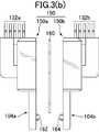
- 3 (a) and 3 (b) are views showing the external appearance of two housing members constituting a housing according to an embodiment of the present invention.
- 3A is a front view of the two housing members 150a and 150b constituting the housing 150 as viewed from the front (X2 side)
- FIG. 3B is a plan view of the two housing members 150a and 150b upward (Z It is the top view seen from the upper direction of an axial direction.
- the housing 150 can be integrally formed with two terminal groups arranged facing each other in the fitting direction, and can cover at least a part of the plurality of terminals. Further, the housing 150 may be any method as long as it can press-fit a plurality of terminals, and can hold the plurality of terminals in the housing 150, in addition to being integrally molded with the two terminal groups.
- one housing member 150a has a protrusion 162a, a protrusion 162b, a protrusion 162c, a protrusion 162d, on a side surface (refer to the mating surface 170a, FIG. 4) facing the other housing member 150b.
- a protrusion group 162 including the protrusion 162e is provided.
- the protrusion group 162 includes five protrusions.
- the protrusion group 162 is not limited to five, and there may be one or more protrusions.
- positions at the surface of the back side of the joint convex part 104a it is not limited to this arrangement
- the other housing member 150b has a protrusion group 164 including a protrusion 164a, a protrusion 164b, a protrusion 164c, a protrusion 164d, and a protrusion 164e on the side surface (matching surface 170b, see FIG. 4) facing the one housing member 150a.
- the protrusion group 164 includes five protrusions.
- the protrusion group 164 is not limited to five. Although it arrange
- the protrusion 162a, the protrusion 162b, the protrusion 162c, the protrusion 162d, and the protrusion 164e included in the protrusion group 162 are between the portions where the housing member 150a holds a plurality of terminals on the surface of the mating surface 170a (see FIG. 4). Or it is arranged next to each other. In the embodiment shown in FIG. 3 (a), the protrusion 162a, the protrusion 162b, the protrusion 162c, between the portions where the plurality of terminals (contact portions 130) exposed from the fitting protrusion 104a are held or on the adjacent surface. A protrusion 162d and a protrusion 162e are respectively disposed.
- the protrusion 164a, the protrusion 164b, the protrusion 164c, the protrusion 164d, and the protrusion 164e included in the protrusion group 164 also have a housing member 150b holding a plurality of terminals on the surface of the mating surface 170b (see FIG. 4). Arranged between or next to the parts. In the embodiment shown in FIG. 3 (a), the protrusion 164a, the protrusion 164b, the protrusion 164c, between the portions where the plurality of terminals (contact portions 130) exposed from the fitting protrusion 104b are held or on the adjacent surfaces. A protrusion 164d and a protrusion 164e are arranged.
- the protrusion group 162 and the protrusion group 164 are arranged at positions facing each other. That is, the protrusion group 162 and the protrusion group 164 are disposed at positions where the distance from the distal end side (X2) of the connector is equal.
- the arrangement is not limited to this, and any one of the protrusion group 162 and the protrusion group 164 is disposed closer to the front end side (X2 side) or the rear end side (X1 side) than the other protrusion group.
- a part of the plurality of protrusions included in the protrusion group 162 may be disposed closer to the front end side (X2 side) or the rear end side (X1 side) than a part of the plurality of protrusions included in the protrusion group 164. Good.
- the housing member 150a and the housing member 150b sandwich and hold the plate 160, which is a conductive member, at a position between one terminal group held by the housing member 150a and the other terminal group held by the housing member 150b. Can do.
- the plate 160 may be any conductive material such as a metal plate or a conductive resin.
- the housing 150 is composed of two members, a first housing member 150a that holds one of the two terminal groups and a second housing member 150b that holds the other terminal group.
- the present invention is not limited to this, and the housing 150 can be integrally formed including the terminal group and the plate 160 (conductive member).
- the number of the plates 160 is one, but the number is not limited to this, and one conductive plate is divided into a plurality of partial plates to form a conductive plate composed of a plurality of partial plates. Sex plates can also be constructed.
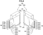
- FIG. 4 is a view showing the accommodating portion provided on the mating surface of the two housing members shown in FIGS. 3 (a) and 3 (b).
- One housing member 150a includes a fitting hole group 166 including a fitting hole 166a, a fitting hole 166b, a fitting hole 166c, a fitting hole 166d, and a fitting hole 166e on the mating surface 170a.
- the fitting hole group 166 includes five fitting holes. However, the number is not limited to five, and one or more fitting holes may be provided. Although it arrange
- the other housing member 150b includes a fitting hole group 168 including a fitting hole 168a, a fitting hole 168b, a fitting hole 168c, a fitting hole 168d, and a fitting hole 168e on the mating surface 170b.
- the fitting hole group 168 includes five fitting holes. However, the number is not limited to five, and one or more fitting holes may be provided. Although it arrange
- the joint hole 168b, the fitting hole 168c, the fitting hole 168d, and the fitting hole 168e are arranged at positions facing each other, and when the housing 150 is configured by combining the housing member 150a and the housing member 150b, the protrusion 162a, The protrusion 162b, the protrusion 162c, the protrusion 162d, and the protrusion 162e are press-fitted and fitted into the fitting hole 168a, the fitting hole 168b, the fitting hole 168c, the fitting hole 168d, and the fitting hole 168e, respectively.
- the fitting hole 166a, the fitting hole 166b, the fitting hole 166c, the fitting hole 166d, and the fitting hole 166e are arranged at positions facing each other, and when the housing 150 is configured by combining the housing member 150a and the housing member 150b,
- the protrusion 164a, the protrusion 164b, the protrusion 164c, the protrusion 164d, and the protrusion 164e are press-fitted and fitted into the fitting hole 166b, the fitting hole 166c, the fitting hole 166d, and the fitting hole 166e, respectively.
- each of the plurality of protrusions included in the protrusion groups 162 and 164 is provided with a rib that protrudes the side surface in the fitting direction of the connector, but is not limited thereto. Ribs can be provided on the side surfaces in the vertical direction (arrangement direction of the protrusions).
- each protrusion included in the protrusion groups 162 and 164 has a tapered quadrangular prism shape, but is not limited to this shape, and can be fitted into each fitting hole such as a circle or a polygon. Any shape may be used as long as it has a shape.
- each fitting hole included in the fitting hole groups 166 and 168 has a rectangular tube shape, but is not limited to this shape, and can be fitted to each protrusion such as a circle or a polygon. Any shape may be used as long as it has a shape.
- the respective fitting holes are closed by being fitted into the respective fitting holes so that the respective fitting holes are closed. This eliminates (or reduces) the gap between the two terminals, and the change in the structure inside the housing holding the two terminal groups can be minimized, and impedance matching can be easily achieved.
- the projections 162 and 164 are fitted into the fitting holes of the fitting hole groups 168 and 166, so that the housing member 150a and the housing member 150b constituting the housing 150 are displaced or deformed. And the high frequency characteristics of the connector can be kept stable.
- the fitting holes 166b, the fitting holes 166c, and the fitting holes 166d are alternately arranged in the vertical direction.
- the protrusions 164a, 164b, 164c, and 164d included in the protrusion group 164 and the fitting holes 168a and 168b included in the fitting hole group 168 are fitted.
- the holes 168c and the fitting holes 168d are alternately arranged in the vertical direction.
- the protrusions 162a, protrusions 162b, protrusions 162c, protrusions 162d, and protrusions 162e included in the protrusion group 162 are arranged side by side in the vertical direction, and the housing member 150b.
- the protrusions 164a, 164b, protrusions 164c, protrusions 164d, and protrusions 164e included in the protrusion group 164 are arranged side by side in the vertical direction.
- the protrusion 162 a, the protrusion 162 b, the protrusion 162 c, the protrusion 162 d, and the protrusion 162 e included in the protrusion group 162 are on the surface of the mating surface 170 a.
- the housing member 150a is positioned between or adjacent to the portions holding the plurality of terminals included in the terminal group, the housing member 150a can be arranged in a straight line or a curved line.
- the protrusions 164a, 164b, protrusions 164c, and protrusions 164d included in the protrusion group 164 can be similarly arranged.
- the arrangement of the fitting holes is not limited to the embodiment shown in FIG. 4.
- the fitting holes 166 a, the fitting holes 166 b, the fitting holes 166 c, and the fitting holes 166 d included in the fitting hole group 166 are included.
- the fitting hole 166e is a position on the surface of the mating surface 170a where the housing member 150a is disposed so as to overlap each of the portions holding the plurality of terminals included in the terminal group, the fitting hole 166e is linear or curved. Etc. can be arranged side by side freely.
- the fitting holes 168a, the fitting holes 168b, the fitting holes 168c, the fitting holes 168d, and the fitting holes 168e included in the fitting hole group 168 can be similarly arranged.
- a trace that is, a hole formed without an insulating synthetic resin flowing in by a jig for supporting a plurality of terminals included in the terminal group can be used.
- a material such as an insulating synthetic resin is used.
- the plurality of holes generated after the jig is fixed and removed are fitted into the fitting holes 166a, 166b, 166c, 166d, 166e, 168a, 168b, 168c, 168d, 168e of the mating surfaces 170a, 170b of the housing members 150a and 150b.
- a plurality of holes generated when the housing members 150a and 150b are integrally molded are formed in the mating surfaces 170a and 170b of the housing members 150a and 150b, and the fitting holes 166a, 166b, 166c, 166d, and 166e are formed.
- 168a, 168b, 168c, 168d, and 168e are not used to form a hole in the outer surface of the housing 150 formed by combining the housing member 150a and the housing member 150b, thereby affecting the high frequency characteristics from the outside. Can be reduced.
- the fitting holes 168e are arranged with a half-pitch shift on the mating surface 170a.
- the fitting holes 168d and the fitting holes 168e are arranged with a half-pitch shift on the mating surface 170b.
- the mating surfaces 170a and 170b are provided with receiving portions 172 and 174, respectively.
- the accommodating portions 172 and 174 are formed by processing the mating surfaces 170 a and 170 b into a concave shape in accordance with the shape of the plate 160 in order to accommodate the plate 160 that is a conductive member.
- a vertical portion (a diagram in which a plurality of terminals included in one terminal group are arranged in a direction perpendicular to the substrate at a position where the plate 160 is accommodated (that is, a position where the accommodating portion 172 is located). 5 (a) or (b)) is held.
- a plurality of terminals included in the other terminal group are arranged in a direction perpendicular to the substrate at a position where the plate 160 is accommodated (that is, a position where the accommodating portion 174 is located). The portion (see FIG. 5 (a) or (b)) is retained.
- the accommodating portion 172 and the accommodating portion 174 are provided on the mating surfaces 170a and 170b, respectively.
- the present invention is not limited to this, and the accommodating portion is provided on at least one of the two mating surfaces. Can also be provided.
- the shape of the accommodating portion is not limited to the concave surface, and can be appropriately changed according to the shape of the plate which is a conductive member.
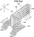
- FIGS. 5 (a) and 5 (b) are views showing a state in the housing of a conductive plate disposed between two terminal groups held by the housing according to the embodiment of the present invention.
- 5A and 5B except for the housing 150, the shape of a plurality of terminals included in the terminal group 134, the arrangement of each terminal, and the positional relationship of the plate 160 sandwiched between the two terminal groups are shown. Show.
- One terminal group (first terminal group) held by the housing member 150a includes the terminals 1 to 5 and the other terminal group (second terminal group) held by the housing member 150b is the terminal 6.
- Two terminals constitute one terminal pair corresponding to differential transmission.
- terminal 1 and terminal 2 are respectively a pair of terminals for transmitting electrical signals.
- terminals 3 and 8 are ground terminals, and are respectively disposed between the terminal pairs.
- Each terminal and ground terminal of the terminal pair can be arranged in parallel along the shape of each other, and can be arranged adjacent to each other on the same plane (for example, XZ plane, XY plane).
- the terminal group 134 has terminals 1 to 5 and terminals 6 to 10 extending in the board direction (below the Z axis) extending rearward (X1 side) along the connector fitting direction from the front end to the rear end. And a bent portion 138 formed by bending the terminals 1 to 5 and the terminals 6 to 10 extending in the board direction to the outside of the connector in a direction perpendicular to the fitting direction of the connector (Y-axis direction). And a bent portion 140 that sequentially bends the terminals 1 to 5 and the terminals 6 to 10 extending in the axial direction to the rear side (X1 side) along the fitting direction of the connector.
- the terminal mounting parts 132 (132a, 132b) are arranged adjacent to each other in the horizontal direction (Y-axis direction) by changing the direction by 90 degrees with respect to the contact parts 130 arranged in the vertical direction (Z-axis direction).
- the horizontal plane of the terminal mounting portion 132 is bent by the bent portion 136, the bent portion 138, and the bent portion 140, changed in direction by 90 degrees, and contacted in the vertical direction. It continues to 130 planes.
- a plurality of terminals included in the terminal group 134 held by the housing 150 are parallel to each other on the same plane (eg, XZ plane, XY plane).
- the change in the interval between the plurality of terminals can be changed. It can be reduced, and deterioration of high frequency characteristics caused by impedance matching disturbance or the like can be suppressed.
- the ground terminal 3 between the terminal pair consisting of the terminals 1 and 2 and the terminal pair consisting of the terminals 4 and 5, it is possible to suppress the occurrence of crosstalk that may occur between the terminal pairs.
- the ground terminal 8 is arranged between the terminal pair consisting of the terminals 6 and 7 and the terminal pair consisting of the terminals 9 and 10, the occurrence of crosstalk that may occur between the terminal pairs can be suppressed. .
- the ground terminals between the terminal pairs it is possible to reduce the adverse electrical effects that can occur between the terminal pairs, particularly in high-speed transmission, and to improve the electrical characteristics.
- each of the two terminal groups has a vertical portion in which a plurality of terminals are arranged in a direction perpendicular to the board on which the connector is mounted, that is, a contact portion on the tip side (X2 side).
- a portion from 130 to a bent portion 138 on the rear end side (X1 side) is included.
- the plate 160 is sandwiched and held between the vertical portion of one terminal group held by the housing member 150a and the vertical portion of the other terminal group held by the housing member 150b by the housing member 150a and the housing member 150b.
- the housing 150 holding the terminal group 134 is divided into a housing member 150a holding one terminal group and a housing member 150b holding the other terminal group, and each terminal included in one terminal group is divided. And a portion of each of the terminals included in the other terminal group are arranged to face each other in the vertical direction (that is, between the vertical portions of the two terminal groups).
- the occurrence of crosstalk between one terminal group and the other terminal group can be suppressed, and adverse electrical effects on high frequency characteristics can be reduced or avoided.
- the plate 160 is disposed so as to partially block between the vertical portions of the two terminal groups except for a part of the tip of the contact portion 130.
- the present invention is not limited to this, and the vertical portion of the two terminal groups may be completely blocked.
- FIG. 6 is a cross-sectional view of an outer conductor shell of a connector including a conductive plate according to an embodiment of the present invention cut in a vertical direction (Z-axis direction) along a fitting direction (X-axis direction).
- the plate 160 is accommodated in the accommodating portion 174 provided on the mating surface 170b of the housing member 150b without any gap. The same applies to the cross section on the housing 150a side.
- the plate 160 By accommodating the plate 160 in the accommodating portions 172 and 174 in this way, as shown in FIGS. 5A and 5B, the vertical portion of one terminal group held by the housing member 150a and the housing member 150b
- the plate 160 can be held at a position between the vertical portion of the other terminal group held by the second terminal group, and the two terminal groups can be electrically disconnected.
- the plate 160 which is a conductive member, is not in electrical contact with members other than the housing member 150a and the housing member 150b.
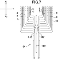
- the present invention is not limited to this. It may be in electrical contact with at least one of the terminal 3 and the terminal 8 (ground terminal) included in the group 134 (see FIG. 7), or may be in electrical contact with the external conductor shell 106 (see FIG. 8).
- the connector 100 may be directly mounted on the substrate 300 (see FIG. 9).
- FIG. 7 is a view showing a state in which a conductive plate according to the second embodiment of the present invention is arranged between two terminal groups.
- the plate 160 is connected to the terminals 3 and 8 as the ground terminals among the terminals 1 to 10 constituting the terminal group 134 as necessary. Can be brought into electrical contact with each other through the heel contact piece 142.
- the plate 160 is in electrical contact with the ground terminal by the two hook contact pieces 142, but is not limited to this, and at least one ground terminal (terminal 3 or terminal 8). As long as it is in electrical contact.
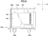
- FIG. 8 is a cross-sectional view of an outer conductor shell of a connector provided with a conductive plate according to a third embodiment of the present invention, cut perpendicularly from the center along the fitting direction.
- the plate 160 is provided with a contact piece provided on the outer conductor shell 106 at the rear end edge (X1 side edge) as necessary. Electrical contact can be made via 144.
- the contact piece 144 is provided at the edge on the rear end side (X2 side) of the plate 160.
- the present invention is not limited to this.
- One or more contact pieces can be provided at other positions where the portion or plate 160 can be in electrical contact with the outer conductor shell 106.
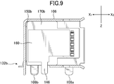
- FIG. 9 is a cross-sectional view of an outer conductor shell of a connector provided with a conductive plate according to a fourth embodiment of the present invention, cut perpendicularly from the center along the fitting direction.
- the plate 160 can be mounted on the substrate 300 by providing the mounting portion 146 on the plate 160 as necessary.
- the mounting portion 146 is provided below the plate 160, but the present invention is not limited to this, and other portions that can electrically contact the front and rear edges of the plate 160 or the plate 160 with the substrate 300.
- the mounting portion 146 can be provided at the position.
- the conductive plate 160 is directly or indirectly (external conductor shell 106 or ground terminal (terminals 3 and 8). ),
- the plate 160 serves as a ground electrode and can contribute to the achievement of high frequency characteristics necessary for high-speed transmission of electrical signals. Further, in any plate 160 of the second to fourth embodiments, the occurrence of crosstalk between the two terminal groups can be suppressed, and the adverse electrical effect on the high frequency characteristics can be reduced or avoided.
- the connector according to the present invention can be used when connecting devices with cables in order to transmit high-frequency electrical signals by electronic devices such as measuring devices that handle high-frequency signals.
- Terminal (Ground terminal) 100 connector 102 fitting recess 104, 104a, 104b fitting projection 106 outer conductor shell 108a, 108b shell mounting part 110 lock hole 112 rear wall part 114 shell mounting part 116 press-fitting claw 118 press-fitting part 120 engaging protrusion 122 engaging Hole 124 Bending piece 126 Support protrusion 130 Contact portion 132, 132a, 132b Terminal mounting portion 134 Terminal group 136, 138, 140 Bending portion 142, 144 Contact piece 146 Plate mounting portion 150 Housing 150a, 150b Housing member 152 Projecting side wall 156 Terminal Protection part 158 Protection piece 160 Plate 162 Protrusion group 162a, 162b, 162c, 162d 162e Protrusion 164 Protrusion group 164a, 164b, 164c, 164d 164e Protrusion 166 Fitting hole group 166a, 166b, 166c, 166d 16 6e fitting hole 168 fitting hole group group
Landscapes
- Details Of Connecting Devices For Male And Female Coupling (AREA)
- Coupling Device And Connection With Printed Circuit (AREA)
Abstract
基板上の回路配線スペース等の確保のために、基板上に実装される基板側コネクタを小型化した場合、コネクタの外部導体シェル内の絶縁性のハウジングに保持される一方の端子群と他方の端子群との間の間隔はより狭くなるため、それらの端子群間で生じるクロストーク等の電気的悪影響を低減又は回避することが困難となるという技術的な課題が生じ得る。この課題を解決するために、ハウジング(150)を第1の端子群を保持する第1のハウジング部材(150a)と第2の端子群を保持する第2のハウジング部材(150b)とに分けて構成し、第1及び第2のハウジング部材(150a、b)を合わせる面(合わせ面)の少なくともいずれか一方に、導電性部材のプレート(160)を収容するための収容部(172、174)を設けて、第1の端子群と第2の端子群との間を、導電性のプレート(160)で電気的に遮ることで、クロストークの発生を抑えることができ、高周波特性への電気的悪影響を低減又は回避することが可能なコネクタを提供する。
Description
本発明は、電気信号の高速伝送に適したコネクタに関する。具体的には、コネクタが備える複数の端子が近接して配列された際に、端子同士が互いの容量あるいは誘導により生じ得るクロストークの発生を防止することが可能な絶縁性のハウジング内の構造に関する。
電気信号等を伝送する際に使用するコネクタには、一般的に、一方の端子群と他方の端子群を向い合せで保持する絶縁性のハウジングと、当該ハウジングを収容する外部導体シェルを備えるものがあり、そのようなコネクタには、端子間の容量あるいは誘導により複数の端子が互いに結合し合うことで生じるクロストーク等の電気的悪影響を低減又は回避するために、一方の端子群と他方の端子群との間に、板状の導電性部材を備えるものがある。
例えば、特開2015-179591公報(特許文献1)に記載のコネクタは、互いに間隔をおいて配置された複数の端子であって、上部に配列された一方の端子群と、下部に配列された他方の端子群が向かい合うように配列された複数の端子と、各端子を保持する絶縁性の保持部材(ハウジング)と、各端子を保持したハウジングを覆う金属製のシェル(外部導体シェル)とを備え、一方の端子群と他方の端子群との間に、一枚の金属板を打ち抜き形成されたグランド部材を備えている。このような構成により、クロストークが原因で生じるインピーダンス整合等のコネクタの高周波特性への電気的悪影響をある程度低減することが可能となる。
近年、計測機器、音響・映像(AV)機器等の電子機器に搭載されたデータ処理装置の能力が向上し、電子機器において膨大なデータを処理できるようになり、それに伴って、大量のデータが電気信号としてコネクタを介して高速に送受信されるようになった。このような高周波の電気信号を適切に伝送するために、一方の端子群と他方の端子群を向い合せで保持する絶縁性のハウジングを備える従来型のコネクタでは、それぞれの端子群に含まれる複数の端子が一定の間隔を保つように絶縁性のハウジングに保持されることで、複数の端子間で生じ得るインピーダンス整合等の乱れを低減し、望ましい高周波特性を得ることができる。
しかしながら、基板上の回路配線スペース等の確保のために、基板上に実装される基板側コネクタの小型化した場合、絶縁性のハウジングに保持される一方の端子群と他方の端子群との間の間隔はより狭くなるため、それらの端子群間で生じるクロストーク等の電気的悪影響を低減又は回避することが困難となる。例えば、特開2015-179591公報(特許文献1)に記載のコネクタでは、板状の導電性部材(グランド部材)によって、一方の端子群と他方の端子群との間を遮っているが、それら端子群の対向する先端側部分の間、及び、対向する後端側部分の間を十分に電気的に遮っておらず、クロストークの発生等の電気的悪影響を十分に防ぐことができない。
以上のような課題を解決するために、コネクタの嵌合方向に沿って対向するように配置された2つの端子群と、該端子群を保持する絶縁性のハウジングと、該ハウジングを収容する外部導体シェルとを備える基板側コネクタにおいて、ハウジングを第1の端子群を保持する第1のハウジング部材と第2の端子群を保持する第2のハウジング部材とに分けて構成し、第1及び第2のハウジング部材がそれぞれ対向する側面(つまり、コネクタの嵌合方向の中心軸側の側面、以下「合わせ面」という)の少なくともいずれか一方に、導電性のプレートを収容するための収容部を設けて、第1の端子群に含まれる複数の端子と第2の端子群に含まれる複数の端子とが近接して垂直方向に対向して配列された間に導電性のプレートを配置することで、第1の端子群と第2の端子群を電気的に遮断し、クロストークの発生を抑えることができ、高周波特性への電気的悪影響を低減又は回避することが可能なコネクタを提供する。
本発明の1つの実施形態に係るコネクタは、
コネクタの嵌合方向に沿って対向するように配置された第1の端子群と第2の端子群を含む端子群と、該端子群を保持した絶縁性のハウジングとを少なくとも含むコネクタであって、
前記ハウジングは、前記第1の端子群を保持する第1のハウジング部材と、前記第2の端子群を保持する第2のハウジング部材とから構成され、
前記第1のハウジング部材と第2のハウジング部材との間に、導電性部材を含むことを特徴とする。
コネクタの嵌合方向に沿って対向するように配置された第1の端子群と第2の端子群を含む端子群と、該端子群を保持した絶縁性のハウジングとを少なくとも含むコネクタであって、
前記ハウジングは、前記第1の端子群を保持する第1のハウジング部材と、前記第2の端子群を保持する第2のハウジング部材とから構成され、
前記第1のハウジング部材と第2のハウジング部材との間に、導電性部材を含むことを特徴とする。
本発明に係るコネクタの好ましい実施形態として、
前記端子群は、前記コネクタを実装する基板に対して垂直方向に複数の端子が並べられた垂直部分を含み、
前記導電性部材は、前記第1の端子群の前記垂直部分と前記第2の端子群の前記垂直部分との間で、前記第1のハウジング部材と前記第2のハウジング部材によって挟まれたことを特徴とする。
前記端子群は、前記コネクタを実装する基板に対して垂直方向に複数の端子が並べられた垂直部分を含み、
前記導電性部材は、前記第1の端子群の前記垂直部分と前記第2の端子群の前記垂直部分との間で、前記第1のハウジング部材と前記第2のハウジング部材によって挟まれたことを特徴とする。
本発明に係るコネクタの好ましい実施形態として、
前記第1のハウジング部材の前記第2のハウジング部材に対向する側面である第1の合わせ面、及び、前記第2のハウジング部材の前記第1のハウジング部材に対向する側面である第2の合わせ面の少なくとも一方に、前記導電性部材を収容するための収容部を設けたことを特徴とする。
前記第1のハウジング部材の前記第2のハウジング部材に対向する側面である第1の合わせ面、及び、前記第2のハウジング部材の前記第1のハウジング部材に対向する側面である第2の合わせ面の少なくとも一方に、前記導電性部材を収容するための収容部を設けたことを特徴とする。
本発明に係るコネクタの好ましい実施形態として、
前記導電性部材は、複数枚の部分導電性部材から構成されたことを特徴とする。
前記導電性部材は、複数枚の部分導電性部材から構成されたことを特徴とする。
本発明に係るコネクタの好ましい実施形態として、
前記第1の端子群及び前記第2の端子群は、それぞれ接触部と端子実装部とを有しており、前記第1の端子群及び前記第2の端子群における接触部の配列方向と端子実装部の配列方向とが互いに直交するように配置されていることを特徴とする。
前記第1の端子群及び前記第2の端子群は、それぞれ接触部と端子実装部とを有しており、前記第1の端子群及び前記第2の端子群における接触部の配列方向と端子実装部の配列方向とが互いに直交するように配置されていることを特徴とする。
本発明に係るコネクタの好ましい実施形態として、
前記導電性部材は、前記第1の端子群の前記垂直部分と前記第2の端子群の前記垂直部分との間を遮る形状であることを特徴とする。
前記導電性部材は、前記第1の端子群の前記垂直部分と前記第2の端子群の前記垂直部分との間を遮る形状であることを特徴とする。
本発明に係るコネクタの好ましい実施形態として、
前記第1の端子群及び前記第2の端子群は、それぞれ2つの端子からなる端子ペアを少なくとも1組以上含むことを特徴とする。
前記第1の端子群及び前記第2の端子群は、それぞれ2つの端子からなる端子ペアを少なくとも1組以上含むことを特徴とする。
本発明に係るコネクタの好ましい実施形態として、
前記第1の端子群及び前記第2の端子群は、2組以上の前記端子ペアと、1以上のグランド端子を含み、
前記グランド端子は、前記端子ペアの各々の間に配置されたことを特徴とする。
前記第1の端子群及び前記第2の端子群は、2組以上の前記端子ペアと、1以上のグランド端子を含み、
前記グランド端子は、前記端子ペアの各々の間に配置されたことを特徴とする。
本発明に係るコネクタの好ましい実施形態として、
前記導電性部材は、前記第1の端子群に含まれるグランド端子及び前記第2の端末群に含まれるグランド端子の少なくとも一方に電気的に接続されていることを特徴とする。
前記導電性部材は、前記第1の端子群に含まれるグランド端子及び前記第2の端末群に含まれるグランド端子の少なくとも一方に電気的に接続されていることを特徴とする。
本発明に係るコネクタの好ましい実施形態として、
前記コネクタは、前記ハウジングを収容する外部導体シェルをさらに備えたことを特徴とする。
前記コネクタは、前記ハウジングを収容する外部導体シェルをさらに備えたことを特徴とする。
本発明に係るコネクタの好ましい実施形態として、
前記導電性部材は、前記外部導体シェルと電気的に接続されていることを特徴とする。
前記導電性部材は、前記外部導体シェルと電気的に接続されていることを特徴とする。
本発明に係るコネクタの好ましい実施形態として、
前記導電性部材は、基板に実装するための実装部を含むことを特徴とする。
前記導電性部材は、基板に実装するための実装部を含むことを特徴とする。
本発明に係るコネクタは、2つの端子群を保持するハウジングを、第1の端子群を保持する第1のハウジング部材と、第2の端子群を保持する第2のハウジング部材とに分けて、第1の端子群に含まれる各端子の一部分と第2の端子群に含まれる各端子の一部分とが垂直方向に対向して配列された間を、導電性のプレートで電気的に遮ることで、第1の端子群と第2の端子群間のクロストークの発生を抑えることができ、高周波特性への電気的悪影響を低減又は回避することができる。
以下に図面を参照して、本発明の実施形態について説明する。なお、実施の形態を説明するための全ての図において、同一部材には原則として同一の符号を付し、その繰り返しの説明は省略する。また、それぞれの実施形態は、独立して説明されているが、互いの構成要素を組み合わせてコネクタを構成することを排除するものではない。
図1は、基板側のコネクタ及びケーブル側のコネクタの外観を示す図である。コネクタの嵌合方向は、図中のX1―X2方向(X軸方向)である。基板側のコネクタ100の先端側はX2方向側であり、ケーブル側のコネクタ200の先端側はX1方向側である。基板300に対して垂直な面はX―Z平面であり、基板300に対して水平な面(平行な面)はX―Y平面である。図中のZ軸方向に沿って上方及び下方を、それぞれのコネクタの上下とする。以上の事項は、その他の図においても同様である。
基板側のコネクタ100は、ケーブル側のコネクタ200との接続側(X2方向側)に嵌合凸部104を形成する複数の端子を保持する合成樹脂等の絶縁性の材料で成型されたハウジング150(図3(a)又は(b)参照)と、ハウジング150を内部に含む外部導体シェル106とから構成される。外部導体シェル106は、当該外部導体シェル106を基板300に実装して固定するためのシェル実装部108a及び108bを含む。シェル実装部108a及び108bは、基板300に設けられた孔に挿入され、半田付けされるディップ端子であるが、基板の表面に実装可能な端子でも良い。シェル実装部108aは、シェル実装部108bよりもコネクタ100の先端側(X2側)の側面に設けられる。
また、外部導体シェル106は、ケーブル側のコネクタ200のロック突部206と係合するロック孔110を備える。ロック孔110は、ケーブル側のコネクタ200のロック突部206と係合できる位置に設けられる。図1では、ロック孔110は、コネクタ100の外部導体シェル106の上下(Z軸方向での上下)の側壁に設けられる。ロック孔110は、ロック突部206と係合できる構造であれば、必ずしも外部導体シェルを貫通した孔でなくてもよい。別の実施形態として、基板側のコネクタの外部導体シェルにロック突部を設け、ケーブル側のコネクタの外部導体シェルにロック孔を設けてもよい。
後壁部112は、外部導体シェル106の後方側(X1側)に設けられ、シェル実装部114を先端部分に有する。シェル実装部114は、外部導体シェル106の後壁部112と一体に形成されており、ハウジング150の後壁(X1側の壁)に沿うように外部導体シェル106の後端側に設けられ、シェル実装部も兼ねており、ハウジング150から露出した2つの端子群(端子実装部132aと132b)の間を通って基板300に実装される。
シェル実装部114は、2つの端子群に含まれる複数の端子に対して接地電極の役割を果たすので、信号を伝送する複数の端子のそれぞれの間にグランド端子を設けない実施形態でも、電気信号の高速伝送に必要な高周波特性を維持することができる。それにより、コネクタに含まれる端子の数を減らすことができ、端子の数(すなわち、部品数)を減へらすことで、コネクタの内部構造は簡略化され、インピーダンス整合を容易に調整可能な内部構造にすることができる。
外部導体シェル106に収容されたハウジング150(図3(a)及び(b)参照)は、コネクタ100の嵌合方向に沿って対向するように配置された2つの端子群(図5(a)又は(b)参照)を保持し、2つの端子群に含まれる複数の端子は、外部導体シェル106の後方(X1側)のハウジング150から露出し、露出した各端子に設けられた端子実装部132(132a、132b)によって基板300の表面上に半田付けされて固定される。それぞれの端子実装部132は、基板300に表面実装されるが、基板に設けられた孔に差し込んで実装されるようにディップ端子として構成してもよい。
ケーブル側のコネクタ200は、基板側のコネクタ100との接続側(X1方向側)に嵌合部202を有し、複数の端子を保持するハウジングを内部に収めた外部導体シェル204と、外部導体シェル204の孔から突出したロック突部206と連動するロック操作用ボタン208と、外部導体シェル204とケーブル400との接続部分を覆うカバー部材210とから構成される。
嵌合部202は、基板側のコネクタ100との接続時に、嵌合凹部102(図2(a)又は(b)参照)に挿入される。外部導体シェル204は、ロック突部206を内側から突出させるための孔を側壁に有する。ロック突部206は、基板側のコネクタ100のロック孔110と係合できる位置に設けられる。図1では、ロック突部206は、コネクタ200の外部導体シェル204の上下(Z軸方向での上下)の側壁に設けられる。ロック突部206は、ロック孔110と係合できる構造であればどのような構造でもよい。
ロック突部206は、外部導体シェル204の内部で、ロック操作用ボタン208と連結され、ロック操作用ボタン208を押し込むことに連動して、ロック突部206が押し込まれる。基板側のコネクタ100との接続時に、ロック操作用ボタン208を押し込むことで、ロック突部206がロック孔110から外れて、ケーブル側のコネクタ200は、基板側のコネクタ100から抜くことができる。
図2(a)及び(b)は、本発明の一実施形態に係る基板側コネクタ(以下、単に「コネクタ」と呼ぶ)の外観を示す図である。図2(a)は、コネクタ100を先端側(X2側)上方からみた斜視図であり、図2(b)は、コネクタ100を側面(X2側)からみた正面図である。図2(a)及び(b)に示されるように、外部導体シェル106に収容されたハウジング150(図3(a)又は(b)参照)は、コネクタ100の嵌合方向に沿って対向するように配置された2つの端子群を保持して、嵌合方向の前方(X2側)に嵌合凹部102を形成する。嵌合凹部102は、外部導体シェル106の嵌合側(X2側)に設けられた嵌合凸部104と、外部導体シェル106の内壁との間の空間である。ハウジング150に保持される2つの端子群に含まれる複数の端子の先端部分の接触部130の各々は、配列方向(Z軸方向)に半ピッチずれて並べて配置される。
外部導体シェル106は、一群の端子実装部132間に位置するシェル実装部114側とは反対側(コネクタ100の側部側)に、ハウジング150の端子保護部156を覆った2つのシェル実装部108bを、コネクタ100の後端側に設け、2つの一群の端子実装部132a及び132bは、それぞれシェル実装部114と、コネクタ100の後端側(X1側)の側面に設けられたシェル実装部108bとの間に配置されている。
端子実装部132a及び132bを露出するハウジング150の後方部分は、コネクタの嵌合方向に対して直交する水平方向(Y方向)外側に膨らんだ端子保護部156を含む。端子保護部156は、複数の端子の水平方向(Y軸方向)に折り曲げられて、並んで配置された部分を保護し、後方側(X1側)から端子実装部132を露出する。端子保護部156は、複数の端子の水平方向(Y軸方向)に折り曲げられて、並んで配置された部分を覆って保護し、後方側(X1側)から端子実装部132を露出する。
外部導体シェル106は外側に膨らんだ端子保護部156の形状に合わせて形成されるため、図2(b)に示されるように、外部導体シェル106の後端側(X1側)に設けられたシェル実装部108bは、先端側(X2側)に設けられたシェル実装部108aよりも、嵌合方向に直交する方向(Y方向)で、外部導体シェル106の外側に設けられる。
屈曲片124は、コネクタ100の嵌合凹部102(すなわち、相手側コネクタとの嵌合口)の縁部に設けられ、コネクタ100の外部導体シェル106と、相手側コネクタ(コネクタ200)の嵌合部202とが間違った向きで嵌合させることを防止するための構造である。図2(a)及び(b)に示す実施例では、屈曲片124は、外部導体シェル106の嵌合凹部102の長辺(Z軸方向に延びる側壁)の縁部から延出して内側に折り曲げられ、屈曲片124の先端は、嵌合凹部102の短辺(Y軸方向に延びる側壁)の縁部に達するように設けられているが、この位置に限定されるものではなく、相手側コネクタとの誤嵌合を防止できれば、嵌合凹部102の縁部のどの位置でもよい。
外部導体シェル106は、コネクタの嵌合方向に対して直交する水平方向(Y軸方向)に突出した突状側壁152に設けられた保護片158を、コネクタの嵌合方向に対して直交する水平方向(Y方向)外側に膨らんだ部分である端子保護部156を巻き込むように折り曲げることで、ハウジング150の端子保護部156で保持される端子群を保護することができる。端子保護部156は、ハウジング150(図3(a)又は(b)参照)において、コネクタの嵌合方向に対して直交する水平方向(Y方向)外側に膨らんだ部分である。
図2(a)及び(b)に示す実施例では、外部導体シェル106は、端子保護部156の形状に合わせて、水平方向(Y軸方向)に突出した突状側壁152に、シェル実装部108b及び保護片158を設けており、保護片158は、シェル実装部108aよりも先端側(X2側)に設けられているが、この配置に限定されるものではなく、保護片158とシェル実装部108bとの位置を入れ替えて、シェル実装部108bが、保護片158よりも先端側(X2側)に設けられてもよい。
保護片158は、端子保護部156の形状に合わせて水平方向(Y方向)に突出した外部導体シェル106の突状側壁152に、垂直方向(Z軸方向)に複数のスリットを入れて当該突状側壁152を分割して、分割された突状側壁152のうちの一部分を用いることができ、残りの部分はシェル実装部108bとして用いることができる。図3(a)及び(b)に示す実施例では、水平方向(Y方向)に突出した外部導体シェル106の突状側壁152に、1つのスリットを入れて、突状側壁152をシェル実装部108bと保護片158の2つに分けて、保護片158を端子保護部156の形状に沿って折り曲げている。
図2(a)及び(b)に示す実施例では、水平方向(Y方向)に突出した外部導体シェル106の側面部分に保護片158とシェル実装部108bを1つずつ設けられているが、1つに限定されるものではなく、保護片158が2以上設けてもよく、シェル実装部108bが2以上設けてもよく、及び、保護片158とシェル実装部108bが共に2以上ずつ設けられてもよい。保護片158が2以上設けられている場合に、シェル実装部108bをそれらの間に配置してもよく、シェル実装部108bが2以上設けられている場合に、保護片158をそれらの間に配置してもよい。
保護片158の端部は、端子保護部156(又はハウジング150)の底部を支持するものであるが、当該端部を基板300に表面実装するための表面実装部として用いることもできる。
図3(a)及び(b)は、本発明の一実施形態に係るハウジングを構成する2つのハウジング部材の外観を示す図である。図3(a)は、ハウジング150を構成する2つのハウジング部材150a及び150bを前方(X2側)からみた正面図であり、図3(b)は、2つのハウジング部材150a及び150bを上方(Z軸方向の上方)からみた上面図である。
ハウジング150は、嵌合方向に沿って向かい合わせで配置された2つの端子群と一体成型することができ、複数の端子の少なくとも一部分を覆うことができる。また、ハウジング150は、2つの端子群と一体成型する以外にも、複数の端子をそれぞれ圧入することもでき、ハウジング150に複数の端子を保持できる方法であればどのような方法でもよい。
図3(a)に示されるように、一方のハウジング部材150aは、他方のハウジング部材150bに対向する側面(合わせ面170a、図4参照)に、突起162a、突起162b、突起162c、突起162d、突起162eを含む突起群162を備える。図3(a)及び(b)に示す実施例では、突起群162に含まれる突起は5つであるが、5つに限定されるものではなく、1つ以上あればよく、突起はそれぞれ嵌合凸部104aの裏側の面に配置されるが、この配置に限定されるものではなく、合わせ面170a又は収容部172(図4参照)の表面上にあればよい。
同様に、他方のハウジング部材150bは、一方のハウジング部材150aに対向する側面(合わせ面170b、図4参照)に、突起164a、突起164b、突起164c、突起164d、突起164eを含む突起群164を備える。図3(a)及び(b)に示す実施例では、突起群164に含まれる突起は5つであるが、5つに限定されるものではなく、1つ以上あればよく、突起はそれぞれ嵌合凸部104bの裏側の面に配置されるが、この配置に限定されるものではなく、合わせ面170b又は収容部174(図4参照)の表面上にあればよい。
突起群162に含まれる突起162a、突起162b、突起162c、突起162d、突起164eは、合わせ面170a(図4参照)の表面上において、ハウジング部材150aが複数の端子を保持している部分の間又は隣にそれぞれ配置されている。図3(a)に示す実施例では、嵌合凸部104aから露出する複数の端子(接触部130)が保持されている部分の間又は隣の面上に突起162a、突起162b、突起162c、突起162d、突起162eがそれぞれ配置されている。
同様に、突起群164に含まれる突起164a、突起164b、突起164c、突起164d、突起164eも、合わせ面170b(図4参照)の表面上において、ハウジング部材150bが複数の端子を保持している部分の間又は隣にそれぞれ配置されている。図3(a)に示す実施例では、嵌合凸部104bから露出する複数の端子(接触部130)が保持されている部分の間又は隣の面上に突起164a、突起164b、突起164c、突起164d、突起164eがそれぞれ配置されている。
図3(b)に示されるように、突起群162と突起群164とは、互いに対向する位置に配置される。つまり、突起群162と突起群164とは、コネクタの先端側(X2)からの距離が等しい位置に配置されている。当然のことながら、この配置に限定されるものではなく、突起群162及び突起群164のいずれかが他方の突起群よりも先端側(X2側)又は後端側(X1側)に配置されてもよく、突起群162に含まれる複数の突起の一部が、突起群164に含まれる複数の突起の一部よりも先端側(X2側)又は後端側(X1側)に配置されてもよい。
ハウジング部材150a及びハウジング部材150bは、ハウジング部材150aが保持する一方の端子群とハウジング部材150bが保持する他方の端子群との間の位置で、導電性部材であるプレート160を挟み込んで保持することができる。プレート160は、金属プレート、導電性樹脂などの導電性物質であればどのようなものでもよい。
本実施形態では、ハウジング150は、2つの端子群のうち一方の端子群を保持する第1のハウジング部材150a及び他方の端子群を保持する第2のハウジング部材150bの2つの部材から構成されているが、これに限定されるものではなく、ハウジング150は端子群及びプレート160(導電性部材)を含めて一体に成型することができる。また、本実施形態では、プレート160は1枚であるがこれに限定されるものではなく、1枚の導電性のプレートを複数枚の部分プレートに分割して、複数枚の部分プレートからなる導電性のプレートを構成することもできる。
図4は、図3(a)及び(b)に示した2つのハウジング部材の合わせ面に設けられた収容部を示す図である。一方のハウジング部材150aは、合わせ面170aに、嵌合孔166a、嵌合孔166b、嵌合孔166c、嵌合孔166d、嵌合孔166eを含む嵌合孔群166を備える。図4に示す実施例では、嵌合孔群166に含まれる嵌合孔は5つであるが、5つに限定されるものではなく、1つ以上あればよく、嵌合孔はそれぞれ嵌合凸部104aの裏側の面に配置されるが、この配置に限定されるものではなく、合わせ面170a又は収容部172の表面上にあればよい。
また、同様に、他方のハウジング部材150bは、合わせ面170bに、嵌合孔168a、嵌合孔168b、嵌合孔168c、嵌合孔168d、嵌合孔168eを含む嵌合孔群168を備える。図4に示す実施例では、嵌合孔群168に含まれる嵌合孔は5つであるが、5つに限定されるものではなく、1つ以上あればよく、嵌合孔はそれぞれ嵌合凸部104bの裏側の面に配置されるが、この配置に限定されるものではなく、合わせ面170b又は収容部174の表面上にあればよい。
合わせ面170aに設けられた突起群162に含まれる突起162a、突起162b、突起162c、突起162d、突起162eと、合わせ面170bに設けられた嵌合孔群168に含まれる嵌合孔168a、嵌合孔168b、嵌合孔168c、嵌合孔168d、嵌合孔168eとは、それぞれ対向する位置に配置され、ハウジング部材150aとハウジング部材150bを合せてハウジング150を構成した際に、突起162a、突起162b、突起162c、突起162d、突起162eは、嵌合孔168a、嵌合孔168b、嵌合孔168c、嵌合孔168d、嵌合孔168eにそれぞれ圧入され嵌め合わされる。
同様に、合わせ面170bに設けられた突起群164に含まれる突起164a、突起164b、突起164c、突起164d、突起164eと、合わせ面170aに設けられた嵌合孔群166に含まれる嵌合孔166a、嵌合孔166b、嵌合孔166c、嵌合孔166d、嵌合孔166eとは、それぞれ対向する位置に配置され、ハウジング部材150aとハウジング部材150bを合せてハウジング150を構成した際に、突起164a、突起164b、突起164c、突起164d、突起164eは、嵌合孔166b、嵌合孔166c、嵌合孔166d、嵌合孔166eにそれぞれ圧入され嵌め合わされる。
突起群162、164に含まれる各突起の幅や長さを変えること、及び、嵌合孔群166、168に含まれる各嵌合孔の幅や深さを変えることで、圧入にかかる力を調整することができ、各突起の側面の全部又は一部を突出させたリブ及び各嵌合孔の内壁の全部又は一部を突出させたリブの少なくとも一方を設けることでも、圧入にかかる力を調整することができる。図4に示される実施例では、突起群162、164に含まれる複数の突起の各々は、コネクタの嵌合方向の側面を突出させたリブを設けているが、これに限定されるものではなく、垂直方向(突起の配列方向)の側面にリブを設けることができる。
また、突起群162、164に含まれる各突起は、先細の四角柱形状であるが、この形状に限定されるものではなく、円形、多角形等、各嵌合孔と嵌め合せることが可能な形状であればどのような形状でもよい。同様に、嵌合孔群166、168に含まれる各嵌合孔は角筒形状であるが、この形状に限定されるものではなく、円形、多角形等、各突起と嵌め合せることが可能な形状であればどのような形状でもよい。
合わせ面170a、170bで、ハウジング部材150aとハウジング部材150bを合せた際に、それぞれの嵌合孔にそれぞれの突起が入って嵌合されることで、各嵌合孔は塞がれてハウジング内部の隙間がなくなり(又は小さくなり)、2つ端子群を保持するハウジング内部の構造の変化を最小限に抑えることができ、容易にインピーダンス整合をとることができる。
また、突起群162、164の各突起が、嵌合孔群168、166の各嵌合孔にそれぞれ嵌合されたことで、ハウジング150を構成するハウジング部材150aとハウジング部材150bのズレや変形を防止し、コネクタの高周波特性を安定的に保つことができる。
図4に示されるように、ハウジング部材150aの合わせ面170a上には、突起群162に含まれる突起162a、突起162b、突起162c、突起162dと、嵌合孔群166に含まれる嵌合孔166a、嵌合孔166b、嵌合孔166c、嵌合孔166dとが、垂直方向に交互に並べて配置されている。ハウジング部材150bの合わせ面170b上には、突起群164に含まれる突起164a、突起164b、突起164c、突起164dと、嵌合孔群168に含まれる嵌合孔168a、嵌合孔168b、嵌合孔168c、嵌合孔168dとが、垂直方向に交互に並べて配置されている。
図4に示す実施例では、ハウジング部材150aの合わせ面170a上には、突起群162に含まれる突起162a、突起162b、突起162c、突起162d、突起162eが垂直方向に並べて配列され、ハウジング部材150bの合わせ面170b上には、突起群164に含まれる突起164a、突起164b、突起164c、突起164d、突起164eが垂直方向に並べて配列されている。
突起の配列は、図4に示す実施例に限定されるものではなく、例えば、突起群162に含まれる突起162a、突起162b、突起162c、突起162d、突起162eが、合わせ面170aの表面上において、ハウジング部材150aが端子群に含まれる複数の端子を保持している部分の間又は隣にそれぞれ配置される位置であれば、直線状や曲線状等自由に並べて配列することができる。突起群164に含まれる突起164a、突起164b、突起164c、突起164dについても、同様に配列することができる。
嵌合孔の配列は、図4に示す実施例に限定されるものではなく、例えば、嵌合孔群166に含まれる嵌合孔166a、嵌合孔166b、嵌合孔166c、嵌合孔166d、嵌合孔166eが、合わせ面170aの表面上において、ハウジング部材150aが端子群に含まれる複数の端子を保持している部分にそれぞれ重ねて配置される位置であれば、直線状や曲線状等自由に並べて配列することができる。嵌合孔群168に含まれる嵌合孔168a、嵌合孔168b、嵌合孔168c、嵌合孔168d、嵌合孔168eについても、同様に配列することができる。
ハウジング部材150a及び150bの各々の合わせ面170a、170bの嵌合孔166a、166b、166c、166d、166e、168a、168b、168c、168d、168eには、ハウジング部材150a及び150bを成型する際に、端子群に含まれる複数の端子を支持するための治具によって絶縁性の合成樹脂が流れ込まずに形成された跡(すなわち、孔)を利用することができる。言い換えると、端子群をそれぞれ保持するハウジング部材150a及び150bを一体成型する場合に、複数の端子を金型内の定位置に固定する治具があるために、絶縁性の合成樹脂等の材料が固まって治具を取り外した後に生ずる複数の孔を、ハウジング部材150a及び150bの各々の合わせ面170a、170bの嵌合孔166a、166b、166c、166d、166e、168a、168b、168c、168d、168eとして機能させることができる。
このように、ハウジング部材150a及び150bの各々の合わせ面170a、170bに、ハウジング部材150a及び150bを一体成型した場合に生ずる複数の孔を形成し、嵌合孔166a、166b、166c、166d、166e、168a、168b、168c、168d、168eとして利用することで、ハウジング部材150aとハウジング部材150bを合せて構成されるハウジング150の外面には孔が形成されず、外部からの高周波特性への影響を低減することができる。
突起群162に含まれる突起162a、突起162b、突起162c、突起162d、突起162eと、嵌合孔群168に含まれる嵌合孔168a、嵌合孔168b、嵌合孔168c、嵌合孔168d、嵌合孔168eは、合わせ面170aにおいて半ピッチずれて配列される。同様に、突起群164に含まれる突起164a、突起164b、突起164c、突起164d、嵌合孔164eと、嵌合孔群168に含まれる嵌合孔168a、嵌合孔168b、嵌合孔168c、嵌合孔168d、嵌合孔168eは、合わせ面170bにおいて半ピッチずれて配列される。
合わせ面170a及び170bには、それぞれ収容部172及び174が設けられる。図4に示す実施例では、収容部172及び174は、導電性部材であるプレート160を収容するために、合わせ面170a及び170bをプレート160の形状に合わせて凹面状に加工して形成される。ハウジング部材150a内では、プレート160が収容される位置(すなわち、収容部172がある位置)に、一方の端子群に含まれる複数の端子が基板に対して垂直方向に並べられた垂直部分(図5(a)又は(b)参照)が保持される。同様に、ハウジング部材150b内では、プレート160が収容される位置(すなわち、収容部174がある位置)に、他方の端子群に含まれる複数の端子が基板に対して垂直方向に並べられた垂直部分(図5(a)又は(b)参照)が保持される。
図4に示される実施例では、収容部172及び収容部174は、それぞれ合わせ面170a及び170bに設けられているが、これに限定されるものではなく、2つの合わせ面の少なくとも一方に収容部を設けることもできる。収容部の形状は、凹面に限定されるものではなく、導電性部材であるプレートの形状に合わせて適宜変更することができる。
図5(a)及び(b)は、本発明の一実施形態に係るハウジングに保持される2つの端子群の間に配置された導電性のプレートのハウジング内の状態を示す図である。図5(a)及び(b)では、ハウジング150を除いて、端子群134に含まれる複数の端子の形状、それぞれの端子の配置及び2つの端子群間に挟まれたプレート160の位置関係を示す。ハウジング部材150aで保持される一方の端子群(第1の端子群)は、端子1から端子5を含み、ハウジング部材150bで保持される他方の端子群(第2の端子群)は、端子6から端子10を含む。2つの端子が差動伝送に対応した1組の端子ペアを構成する。図5(a)及び(b)に示す実施形態では、端子1と端子2、端子4と端子5、端子6と端子7、端子9と端子10がそれぞれ電気信号を伝送するための端子ペアとなる。端子3及び端子8は、グランド端子であり、それぞれ端子ペアの間に配置される。端子ペアの各端子及びグランド端子は、互いの形状に沿って平行に配置することができ、同一平面(例えば、X-Z平面、X-Y平面)上に隣り合わせで配置することができる。
また、端子群134は、先端から後端までの間に、コネクタの嵌合方向に沿って後方(X1側)に延びた端子1から5及び端子6から10を基板方向(Z軸の下方)に折り曲げた屈曲部136と、基板方向に延びた端子1から5及び端子6から10を、コネクタの嵌合方向に対して直交する方向(Y軸方向)でコネクタの外側に折り曲げた屈曲部138と、軸直方向に延びた端子1から5及び端子6から10をコネクタの嵌合方向に沿って後部側(X1側)に折り曲げた屈曲部140とを順に備える。
端子実装部132(132a、132b)は、垂直方向(Z軸方向)に並べて配置された接触部130に対して90度向きを変えて水平方向(Y軸方向)に隣り合わせで配置される。すなわち、それぞれの端子において、端子実装部132の水平方向を向いた平面は、屈曲部136、屈曲部138及び屈曲部140によって、折り曲げられて90度向きを変えて、垂直方向を向いた接触部130の平面に続いている。
図5(a)及び(b)に示すように、ハウジング150で保持される端子群134に含まれる複数の端子を、同一平面(例えば、X-Z平面、X-Y平面)上で平行に隣り合わせて配置し、このような一定間隔を保った配置を屈曲部136、屈曲部138、屈曲部140でそれら複数の端子を折り曲げた場合でも維持することによって、複数の端子間の間隔の変化を小さくでき、インピーダンス整合の乱れ等により生じる高周波特性の悪化を抑制することができる。
また、端子1、2からなる端子ペアと端子4、5からなる端子ペアの間にグランド端子3が配置されていることにより、端子ペア間で生じえるクロストークの発生を抑制することができ、同様に、端子6、7からなる端子ペアと端子9、10からなる端子ペアの間にグランド端子8が配置されていることにより、端子ペア間で生じ得るクロストークの発生を抑制することができる。このように、グランド端子を端子ペアの間に配置したことで、特に高速伝送における端子ペア間で生じえる電気的悪影響を低減させ、電気的特性の向上を図ることができる。
図5(a)に示すように、2つの端子群の各々は、コネクタを実装する基板に対して垂直方向に複数の端子が並べられた垂直部分、すなわち、先端側(X2側)の接触部130から後端側(X1側)の屈曲部138までの部分を有する。プレート160は、ハウジング部材150aで保持される一方の端子群の垂直部分とハウジング部材150bで保持される他方の端子群の垂直部分との間で、ハウジング部材150aとハウジング部材150bによって挟み込んで保持される。
このように、端子群134を保持するハウジング150を、一方の端子群を保持するハウジング部材150aと、他方の端子群を保持するハウジング部材150bとに分けて、一方の端子群に含まれる各端子の一部分と他方の端子群に含まれる各端子の一部分とが垂直方向に対向して配列された間(すなわち、2つの端子群の垂直部分の間)を、導電性部材であるプレート160で電気的に遮ることで、一方の端子群と他方の端子群間のクロストークの発生を抑えることができ、高周波特性への電気的悪影響を低減又は回避することができる。
図5(a)及び(b)に示す実施例では、接触部130の先端の一部分を除いて、2つの端子群の垂直部分の間を部分的に遮るようにプレート160が配置されているが、これに限定されるものではなく、2つの端子群の垂直部分間を完全に遮るようにしてもよい。
図6は、本発明の実施形態に係る導電性のプレートを備えるコネクタの外部導体シェルを嵌合方向(X軸方向)に沿って垂直方向(Z軸方向)に切った断面図である。プレート160は、ハウジング部材150bの合わせ面170bに設けられた収容部174に隙間なく収容される。ハウジング150a側の断面についても同様である。このようにプレート160を収容部172、174に収容することにより、図5(a)及び(b)に示したように、ハウジング部材150aで保持される一方の端子群の垂直部分とハウジング部材150bで保持される他方の端子群の垂直部分との間の位置で、プレート160を保持することができ、2つの端子群を電気的に遮断することができる。
図6に示す実施例では、導電性部材であるプレート160は、ハウジング部材150a及びハウジング部材150b以外の部材に電気的に接触していないが、これに限定されるものではなく、プレート160は端子群134に含まれる端子3及び端子8(グランド端子)の少なくとも一方に電気的に接触してもよく(図7参照)、外部導体シェル106に電気的に接触してもよく(図8参照)、コネクタ100を実装する基板300に直接実装してもよい(図9参照)。
図7は、本発明の第2の実施形態に係る導電性のプレートを、2つの端子群の間に配置した状態を示す図である。コネクタによる電気信号の高速伝送の性能をより向上を図るためさせるために、必要に応じて、プレート160を、端子群134を構成する端子1から10のうち、グランド端子である端子3及び端子8にそれぞれ 接触片142を介して電気的に接触させることができる。図7に示す実施例では、プレート160が2つの 接触片142でグランド端子に電気的に接触しているが、これに限定されるものではなく、少なくとも一方のグランド端子(端子3又は端子8)に電気的に接触していればよい。
図8は、本発明の第3の実施形態に係る導電性のプレートを備えるコネクタの外部導体シェルを嵌合方向に沿って中心から垂直に切った断面図である。コネクタによる電気信号の高速伝送の性能をより向上を図るためさせるために、必要に応じて、プレート160を、外部導体シェル106に後端縁部(X1側の縁部)に設けられた接触片144を介して電気的に接触させることができる。図8に示す実施例では、接触片144がプレート160の後端側(X2側)の縁部に設けられているが、これに限定されるものではなく、プレート160の前後縁部、上下縁部又はプレート160を外部導体シェル106に電気的に接触できるその他の位置に、接触片を1以上設けることができる。
図9は、本発明の第4の実施形態に係る導電性のプレートを備えるコネクタの外部導体シェルを嵌合方向に沿って中心から垂直に切った断面図である。コネクタによる電気信号の高速伝送の性能をより向上を図るためさせるために、必要に応じて、プレート160に実装部146を設けて、プレート160を基板300に実装することができる。図9に示す実施例では、実装部146をプレート160の下方に設けているが、これに限定されるものではなく、プレート160の前後縁部又はプレート160を基板300に電気的に接触できるその他の位置に、実装部146を設けることができる。
図7から図9に示す第2から第4の実施形態のいずれの実施形態においても、導電性のプレート160は、直接的に又は間接的に(外部導体シェル106又はグランド端子(端子3,8)を介して)基板300に接続されるので、プレート160は接地電極の役割を果たし、電気信号の高速伝送に必要な高周波特性の達成に寄与することができる。また、第2から第4の実施形態のいずれのプレート160でも、2つの端子群間のクロストークの発生を抑えることができ、高周波特性への電気的悪影響を低減又は回避することができる。
本発明の個々の実施例は、独立したものではなく、それぞれ組み合わせて適宜実施することができる。
本発明に係るコネクタは、高周波信号を扱う計測機器等の電子機器によって、高い周波数の電気信号を伝送するために、機器間をケーブルで接続する際に利用することができる。
1,2,4,5,6,7,9,10 端子
3,8 端子(グランド端子)
100 コネクタ
102 嵌合凹部
104,104a,104b 嵌合凸部
106 外部導体シェル
108a,108b シェル実装部
110 ロック孔
112 後壁部
114 シェル実装部
116 圧入爪
118 圧入部
120 係合突部
122 係合孔
124 屈曲片
126 支持突起
130 接触部
132,132a,132b 端子実装部
134 端子群
136,138,140 屈曲部
142,144 接触片
146 プレート実装部
150 ハウジング
150a,150b ハウジング部材
152 突状側壁
156 端子保護部
158 保護片
160 プレート
162 突起群
162a,162b,162c,162d 162e 突起
164 突起群
164a,164b,164c,164d 164e 突起
166 嵌合孔群
166a,166b,166c,166d 166e 嵌合孔
168 嵌合孔群
168a,168b,168c,168d 168e 嵌合孔
170,170a,170b 合わせ面
172,174 収容部
200 コネクタ
202 嵌合部
204 外部導体シェル
206 ロック突部
208 ロック操作用ボタン
210 カバー部材
212 嵌合凹部
300 基板
400 ケーブル
3,8 端子(グランド端子)
100 コネクタ
102 嵌合凹部
104,104a,104b 嵌合凸部
106 外部導体シェル
108a,108b シェル実装部
110 ロック孔
112 後壁部
114 シェル実装部
116 圧入爪
118 圧入部
120 係合突部
122 係合孔
124 屈曲片
126 支持突起
130 接触部
132,132a,132b 端子実装部
134 端子群
136,138,140 屈曲部
142,144 接触片
146 プレート実装部
150 ハウジング
150a,150b ハウジング部材
152 突状側壁
156 端子保護部
158 保護片
160 プレート
162 突起群
162a,162b,162c,162d 162e 突起
164 突起群
164a,164b,164c,164d 164e 突起
166 嵌合孔群
166a,166b,166c,166d 166e 嵌合孔
168 嵌合孔群
168a,168b,168c,168d 168e 嵌合孔
170,170a,170b 合わせ面
172,174 収容部
200 コネクタ
202 嵌合部
204 外部導体シェル
206 ロック突部
208 ロック操作用ボタン
210 カバー部材
212 嵌合凹部
300 基板
400 ケーブル
Claims (12)
- コネクタの嵌合方向に沿って対向するように配置された第1の端子群と第2の端子群を含む端子群と、該端子群を保持した絶縁性のハウジングとを少なくとも含むコネクタであって、
前記ハウジングは、前記第1の端子群を保持する第1のハウジング部材と、前記第2の端子群を保持する第2のハウジング部材とから構成され、
前記第1のハウジング部材と第2のハウジング部材との間に、導電性部材を含むことを特徴とするコネクタ。 - 前記端子群は、前記コネクタを実装する基板に対して垂直方向に複数の端子が並べられた垂直部分を含み、
前記導電性部材は、前記第1の端子群の前記垂直部分と前記第2の端子群の前記垂直部分との間で、前記第1のハウジング部材と前記第2のハウジング部材によって挟まれたことを特徴とする請求項1に記載のコネクタ。 - 前記第1のハウジング部材の前記第2のハウジング部材に対向する側面である第1の合わせ面、及び、前記第2のハウジング部材の前記第1のハウジング部材に対向する側面である第2の合わせ面の少なくとも一方に、前記導電性部材を収容するための収容部を設けたことを特徴とする請求項1又は2に記載のコネクタ。
- 前記導電性部材は、複数枚の部分導電性部材から構成されたことを特徴とする請求項1から3のいずれか1項に記載のコネクタ。
- 前記第1の端子群及び前記第2の端子群は、それぞれ接触部と端子実装部とを有しており、前記第1の端子群及び前記第2の端子群における接触部の配列方向と端子実装部の配列方向とが互いに直交するように配置されていることを特徴とする請求項1から4のいずれか1項に記載のコネクタ。
- 前記導電性部材は、前記第1の端子群の前記垂直部分と前記第2の端子群の前記垂直部分との間を遮る形状であることを特徴とする請求項5に記載のコネクタ。
- 前記第1の端子群及び前記第2の端子群は、それぞれ2つの端子からなる端子ペアを少なくとも1組以上含むことを特徴とする請求項1から6のいずれか1項に記載のコネクタ。
- 前記第1の端子群及び前記第2の端子群は、2組以上の前記端子ペアと、1以上のグランド端子を含み、
前記グランド端子は、前記端子ペアの各々の間に配置されたことを特徴とする請求項1から6のいずれか1項に記載のコネクタ。 - 前記導電性部材は、前記第1の端子群に含まれるグランド端子及び前記第2の端末群に含まれるグランド端子の少なくとも一方に電気的に接続されていることを特徴とする請求項8に記載のコネクタ。
- 前記ハウジングを収容する外部導体シェルをさらに備えたことを特徴とする請求項1から9のいずれか1項に記載のコネクタ。
- 前記導電性部材は、前記外部導体シェルと電気的に接続されていることを特徴する請求項10に記載のコネクタ。
- 前記導電性部材は、基板に実装するための実装部を含むことを特徴とする請求項1から11のいずれか1項に記載のコネクタ。
Priority Applications (1)
| Application Number | Priority Date | Filing Date | Title |
|---|---|---|---|
| CN201780007528.3A CN108475890B (zh) | 2016-03-18 | 2017-03-16 | 连接器 |
Applications Claiming Priority (2)
| Application Number | Priority Date | Filing Date | Title |
|---|---|---|---|
| JP2016-056192 | 2016-03-18 | ||
| JP2016056192A JP6749114B2 (ja) | 2016-03-18 | 2016-03-18 | コネクタ |
Publications (1)
| Publication Number | Publication Date |
|---|---|
| WO2017159793A1 true WO2017159793A1 (ja) | 2017-09-21 |
Family
ID=59851712
Family Applications (1)
| Application Number | Title | Priority Date | Filing Date |
|---|---|---|---|
| PCT/JP2017/010693 Ceased WO2017159793A1 (ja) | 2016-03-18 | 2017-03-16 | コネクタ |
Country Status (3)
| Country | Link |
|---|---|
| JP (1) | JP6749114B2 (ja) |
| CN (1) | CN108475890B (ja) |
| WO (1) | WO2017159793A1 (ja) |
Cited By (2)
| Publication number | Priority date | Publication date | Assignee | Title |
|---|---|---|---|---|
| CN110504565A (zh) * | 2018-05-18 | 2019-11-26 | 富士康(昆山)电脑接插件有限公司 | 电连接器及其对接连接器 |
| EP3761461A4 (en) * | 2018-03-02 | 2021-12-01 | Hirose Electric Co., Ltd. | METHOD OF MANUFACTURING AN ELECTRICAL CONNECTOR AND ELECTRICAL CONNECTOR |
Families Citing this family (4)
| Publication number | Priority date | Publication date | Assignee | Title |
|---|---|---|---|---|
| WO2020116149A1 (ja) * | 2018-12-04 | 2020-06-11 | 株式会社村田製作所 | 電気コネクタセットおよび該電気コネクタセットの実装構造 |
| JP7600907B2 (ja) * | 2021-07-02 | 2024-12-17 | 株式会社オートネットワーク技術研究所 | 基板用コネクタ |
| CN114824963A (zh) * | 2022-03-30 | 2022-07-29 | 超聚变数字技术有限公司 | 一种连接器和连接器制造的方法 |
| CN115733029B (zh) * | 2022-11-15 | 2025-09-16 | 超聚变数字技术有限公司 | 注塑壳及其形成方法、连接器及其制备方法 |
Citations (4)
| Publication number | Priority date | Publication date | Assignee | Title |
|---|---|---|---|---|
| JP2002042977A (ja) * | 2000-07-31 | 2002-02-08 | Japan Aviation Electronics Industry Ltd | 高速伝送用コネクタ |
| US20140024257A1 (en) * | 2012-07-20 | 2014-01-23 | Speed Tech Corp. | High density connector structure for transmitting high frequency signals |
| US20140194005A1 (en) * | 2013-01-08 | 2014-07-10 | Hon Hai Precision Industry Co., Ltd. | Electrical connector with shieldingthereof |
| JP3198301U (ja) * | 2014-04-14 | 2015-06-25 | アップル インコーポレイテッド | 耐久性コネクタレセプタクル |
Family Cites Families (4)
| Publication number | Priority date | Publication date | Assignee | Title |
|---|---|---|---|---|
| MY174133A (en) * | 2013-01-16 | 2020-03-10 | Molex Inc | Bi-directional latch |
| JP6265803B2 (ja) * | 2014-03-19 | 2018-01-24 | 日本航空電子工業株式会社 | コネクタ |
| CN105337107B (zh) * | 2014-07-11 | 2018-01-16 | 上海莫仕连接器有限公司 | 电连接器及具有该电连接器的线缆连接器 |
| CN204966770U (zh) * | 2015-07-25 | 2016-01-13 | 富士康(昆山)电脑接插件有限公司 | 电连接器 |
-
2016
- 2016-03-18 JP JP2016056192A patent/JP6749114B2/ja active Active
-
2017
- 2017-03-16 CN CN201780007528.3A patent/CN108475890B/zh active Active
- 2017-03-16 WO PCT/JP2017/010693 patent/WO2017159793A1/ja not_active Ceased
Patent Citations (4)
| Publication number | Priority date | Publication date | Assignee | Title |
|---|---|---|---|---|
| JP2002042977A (ja) * | 2000-07-31 | 2002-02-08 | Japan Aviation Electronics Industry Ltd | 高速伝送用コネクタ |
| US20140024257A1 (en) * | 2012-07-20 | 2014-01-23 | Speed Tech Corp. | High density connector structure for transmitting high frequency signals |
| US20140194005A1 (en) * | 2013-01-08 | 2014-07-10 | Hon Hai Precision Industry Co., Ltd. | Electrical connector with shieldingthereof |
| JP3198301U (ja) * | 2014-04-14 | 2015-06-25 | アップル インコーポレイテッド | 耐久性コネクタレセプタクル |
Cited By (3)
| Publication number | Priority date | Publication date | Assignee | Title |
|---|---|---|---|---|
| EP3761461A4 (en) * | 2018-03-02 | 2021-12-01 | Hirose Electric Co., Ltd. | METHOD OF MANUFACTURING AN ELECTRICAL CONNECTOR AND ELECTRICAL CONNECTOR |
| US11271354B2 (en) | 2018-03-02 | 2022-03-08 | Hirose Electric Co., Ltd. | Electric connector manufacturing method and electric connector |
| CN110504565A (zh) * | 2018-05-18 | 2019-11-26 | 富士康(昆山)电脑接插件有限公司 | 电连接器及其对接连接器 |
Also Published As
| Publication number | Publication date |
|---|---|
| CN108475890A (zh) | 2018-08-31 |
| JP6749114B2 (ja) | 2020-09-02 |
| CN108475890B (zh) | 2020-06-16 |
| JP2017174515A (ja) | 2017-09-28 |
Similar Documents
| Publication | Publication Date | Title |
|---|---|---|
| JP6703900B2 (ja) | コネクタおよびコネクタシステム | |
| WO2017159793A1 (ja) | コネクタ | |
| CN214542655U (zh) | 连接器 | |
| JP6583961B2 (ja) | コネクタ | |
| US7909668B2 (en) | Contact with twist pin interface | |
| JP7358562B2 (ja) | コネクタ | |
| JP5854761B2 (ja) | 電気コネクタ | |
| KR20060135964A (ko) | 저 인덕턴스 차폐 커넥터 | |
| JP5640912B2 (ja) | コンタクトユニット、および、それを備えるプリント回路板用コネクタ | |
| US7867045B2 (en) | Electrical connectors and assemblies having socket members | |
| CN108370120B (zh) | 连接器 | |
| WO2017104312A1 (ja) | コネクタ | |
| US20050054226A1 (en) | Balanced transmission cable connector | |
| JP2017103119A (ja) | 電気コネクタ | |
| JP5868140B2 (ja) | 同軸ケーブル接続モジュール、同軸ケーブル用多極コネクタ及び多極複合コネクタ | |
| JP6703861B2 (ja) | コネクタ | |
| JP5318613B2 (ja) | コネクタ | |
| JP6097165B2 (ja) | コネクタ | |
| JP6703860B2 (ja) | コネクタ | |
| JP6833524B2 (ja) | 基板実装用のコネクタ | |
| JP6080922B2 (ja) | 電気コネクタ |
Legal Events
| Date | Code | Title | Description |
|---|---|---|---|
| NENP | Non-entry into the national phase |
Ref country code: DE |
|
| 121 | Ep: the epo has been informed by wipo that ep was designated in this application |
Ref document number: 17766789 Country of ref document: EP Kind code of ref document: A1 |
|
| 122 | Ep: pct application non-entry in european phase |
Ref document number: 17766789 Country of ref document: EP Kind code of ref document: A1 |