WO2017159341A1 - 回路構成体 - Google Patents
回路構成体 Download PDFInfo
- Publication number
- WO2017159341A1 WO2017159341A1 PCT/JP2017/007670 JP2017007670W WO2017159341A1 WO 2017159341 A1 WO2017159341 A1 WO 2017159341A1 JP 2017007670 W JP2017007670 W JP 2017007670W WO 2017159341 A1 WO2017159341 A1 WO 2017159341A1
- Authority
- WO
- WIPO (PCT)
- Prior art keywords
- terminal
- bus bar
- sheet substrate
- electronic component
- circuit board
- Prior art date
- Legal status (The legal status is an assumption and is not a legal conclusion. Google has not performed a legal analysis and makes no representation as to the accuracy of the status listed.)
- Ceased
Links
Images




Classifications
-
- H—ELECTRICITY
- H02—GENERATION; CONVERSION OR DISTRIBUTION OF ELECTRIC POWER
- H02G—INSTALLATION OF ELECTRIC CABLES OR LINES, OR OF COMBINED OPTICAL AND ELECTRIC CABLES OR LINES
- H02G3/00—Installations of electric cables or lines or protective tubing therefor in or on buildings, equivalent structures or vehicles
- H02G3/02—Details
- H02G3/08—Distribution boxes; Connection or junction boxes
- H02G3/16—Distribution boxes; Connection or junction boxes structurally associated with support for line-connecting terminals within the box
-
- H—ELECTRICITY
- H05—ELECTRIC TECHNIQUES NOT OTHERWISE PROVIDED FOR
- H05K—PRINTED CIRCUITS; CASINGS OR CONSTRUCTIONAL DETAILS OF ELECTRIC APPARATUS; MANUFACTURE OF ASSEMBLAGES OF ELECTRICAL COMPONENTS
- H05K1/00—Printed circuits
- H05K1/02—Details
- H05K1/14—Structural association of two or more printed circuits
-
- H—ELECTRICITY
- H05—ELECTRIC TECHNIQUES NOT OTHERWISE PROVIDED FOR
- H05K—PRINTED CIRCUITS; CASINGS OR CONSTRUCTIONAL DETAILS OF ELECTRIC APPARATUS; MANUFACTURE OF ASSEMBLAGES OF ELECTRICAL COMPONENTS
- H05K1/00—Printed circuits
- H05K1/18—Printed circuits structurally associated with non-printed electric components
-
- H—ELECTRICITY
- H05—ELECTRIC TECHNIQUES NOT OTHERWISE PROVIDED FOR
- H05K—PRINTED CIRCUITS; CASINGS OR CONSTRUCTIONAL DETAILS OF ELECTRIC APPARATUS; MANUFACTURE OF ASSEMBLAGES OF ELECTRICAL COMPONENTS
- H05K3/00—Apparatus or processes for manufacturing printed circuits
- H05K3/10—Apparatus or processes for manufacturing printed circuits in which conductive material is applied to the insulating support in such a manner as to form the desired conductive pattern
- H05K3/20—Apparatus or processes for manufacturing printed circuits in which conductive material is applied to the insulating support in such a manner as to form the desired conductive pattern by affixing prefabricated conductor pattern
- H05K3/202—Apparatus or processes for manufacturing printed circuits in which conductive material is applied to the insulating support in such a manner as to form the desired conductive pattern by affixing prefabricated conductor pattern using self-supporting metal foil pattern
-
- H—ELECTRICITY
- H05—ELECTRIC TECHNIQUES NOT OTHERWISE PROVIDED FOR
- H05K—PRINTED CIRCUITS; CASINGS OR CONSTRUCTIONAL DETAILS OF ELECTRIC APPARATUS; MANUFACTURE OF ASSEMBLAGES OF ELECTRICAL COMPONENTS
- H05K7/00—Constructional details common to different types of electric apparatus
- H05K7/02—Arrangements of circuit components or wiring on supporting structure
- H05K7/06—Arrangements of circuit components or wiring on supporting structure on insulating boards, e.g. wiring harnesses
-
- H—ELECTRICITY
- H05—ELECTRIC TECHNIQUES NOT OTHERWISE PROVIDED FOR
- H05K—PRINTED CIRCUITS; CASINGS OR CONSTRUCTIONAL DETAILS OF ELECTRIC APPARATUS; MANUFACTURE OF ASSEMBLAGES OF ELECTRICAL COMPONENTS
- H05K2201/00—Indexing scheme relating to printed circuits covered by H05K1/00
- H05K2201/10—Details of components or other objects attached to or integrated in a printed circuit board
- H05K2201/10227—Other objects, e.g. metallic pieces
- H05K2201/10272—Busbars, i.e. thick metal bars mounted on the printed circuit board [PCB] as high-current conductors
Definitions
- the present invention relates to a circuit structure.
- This application claims priority based on Japanese Patent Application No. 2016-052487 filed on Mar. 16, 2016, and incorporates all the contents described in the aforementioned Japanese application.
- An automobile is equipped with an electrical junction box (also called a power distributor) that distributes power from a power source (battery) to loads such as headlamps and wipers.
- an electrical junction box also called a power distributor
- loads such as headlamps and wipers.
- an electrical junction box also called a power distributor
- a member constituting the internal circuit of the electrical junction box for example, there is a circuit structure shown in Patent Document 1.
- the circuit structure is mounted on a control circuit board on which a conductor pattern (circuit pattern) is formed, an input terminal bus bar and an output terminal bus bar bonded to the control circuit board, and the control circuit board and both bus bars.
- FET Field effect transistor: electronic component
- the FET includes a main body (package), a source terminal and a gate terminal that protrude from the side surface of the main body and extend downward, and a drain terminal provided on the back surface of the main body.
- the drain terminal of the FET is electrically connected to the input terminal bus bar, and the source terminal is electrically connected to the output terminal bus bar.
- the gate terminal of the FET is bent and formed so as to be displaced upward by the thickness of the control circuit board with respect to the source terminal, and is electrically connected to the conductor pattern on the control circuit board on the output terminal bus bar. (Specifications 0036-0039, FIG. 4).
- the circuit structure of the present disclosure is: A circuit board having an upper surface on which a circuit pattern is formed; A plurality of bus bars connected to the circuit board and fixed to the lower surface of the circuit board at intervals, An electronic component having a package disposed on the bus bar and a terminal provided in a contour of a lower surface of the package; A sheet substrate having one end connected to the terminal and the other end disposed outside the contour of the lower surface of the package; The circuit board, the sheet substrate, and an adhesive sheet that bonds the plurality of bus bars.
- FIG. 1 is a perspective view showing an outline of a circuit configuration body according to Embodiment 1.
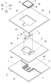
- FIG. 1 is an exploded perspective view showing an outline of a circuit configuration body according to Embodiment 1.
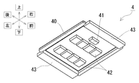
- FIG. 3 is a perspective view illustrating an outline of a lower surface of an electronic component provided in the circuit configuration body according to Embodiment 1.
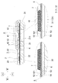
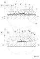
- FIG. 4 is a cross-sectional view showing a state where the circuit structure shown in FIG. 1 is cut along a (IV)-(IV) cutting line.
- FIG. 2 is a cross-sectional view showing a state where the circuit structure shown in FIG. 1 is cut along a (V)-(V) cutting line.
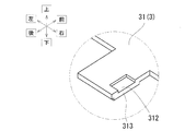
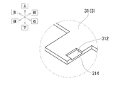
- FIG. 6 is a partially enlarged view showing an example of a recess of a bus bar provided in the circuit configuration body according to Embodiment 2.
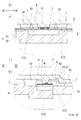
- FIG. An example of the circuit structure according to the second embodiment is shown, and the upper figure is a cross-sectional view showing a state in which the circuit structure is cut along a cutting line passing through the center of the sheet substrate in the vertical direction, and the lower figure shows the circuit structure. It is sectional drawing which shows the state cut
- FIG. 10 is a partial enlarged view showing another example of a recess of a bus bar provided in the circuit configuration body according to the second embodiment.
- FIG. 10 is an exploded perspective view showing an outline of a circuit configuration body according to Modification 1.
- FIG. 10 The circuit structure which concerns on the modification 1 is shown, The upper figure is sectional drawing which shows the state which cut
- an object of the present invention is to provide a circuit structure that can electrically connect a terminal provided in the contour of the lower surface of the electronic component to a connection target outside the contour.
- the circuit structure of this indication can electrically connect the terminal provided in the outline of the undersurface of an electronic component to the connecting object outside the outline.
- a circuit structure includes: A circuit board having an upper surface on which a circuit pattern is formed; A plurality of bus bars connected to the circuit board and fixed to the lower surface of the circuit board at intervals, An electronic component having a package disposed on the bus bar and a terminal provided in a contour of a lower surface of the package; A sheet substrate having one end connected to the terminal and the other end disposed outside the contour of the lower surface of the package; The circuit board, the sheet substrate, and an adhesive sheet that bonds the plurality of bus bars.
- the terminals provided in the contour of the lower surface of the electronic component can be electrically connected to the connection target outside the contour.
- the electronic component since the electronic component has terminals provided in the outline of the lower surface of the package, the length of the terminals is short, electric resistance can be reduced, loss can be easily reduced, and heat dissipation can be improved. Easy to improve.
- the bus bar is formed in an overlapping area with the terminal of the electronic component in the bus bar, and is a recess that relaxes a step with a peripheral area where the sheet substrate is not arranged. It is mentioned to have.
- the electronic component has a terminal within the outline of the lower surface of the package and is not electrically and mechanically connected to the sheet substrate but electrically and mechanically connected to the bus bar.
- it is easy to reduce the vertical step between both terminals. This is because an overlapping area with the notch or the recess of the sheet substrate is easily fitted into the notch or the recess due to the load of the electronic component.
- Embodiment 1 A circuit configuration 1A according to the first embodiment will be described with reference to FIGS. 1 A of circuit structures are provided with the circuit board 2 which has a circuit pattern (not shown), the some bus bar 3 fixed to the circuit board 2, and the electronic component 4 which has a terminal in the outline of the lower surface of the package 40.
- FIG. One of the features of the circuit structure 1A is that a sheet substrate 5 that electrically connects terminals provided in the contour of the lower surface of the package 40 to a connection target outside the contour, the sheet substrate 5 and the bus bar 3 It is in the point provided with the adhesive sheet 6 which adhere
- the circuit board 2 side in the circuit structure 1A is the upper side
- the bus bar 3 side is the lower side
- the parallel direction of the plurality of bus bars 3 is a direction orthogonal to both the front-rear direction, the vertical direction, and the front-rear direction. Is described as the left-right direction.
- the circuit board 2 includes an insulating substrate 20 and a circuit pattern formed on one surface (upper surface) of the insulating substrate 20 to which the electronic component 4 is electrically connected (FIGS. 1 and 2).
- the circuit pattern may also be formed on the other surface (lower surface) of the insulating substrate 20.
- This circuit pattern is formed of copper foil.
- the circuit board 2 can be a printed board.
- the bus bar 3 is fixed to the other surface (lower surface) of the insulating substrate 20.
- the insulating substrate 20 is formed with a mounting through hole 22 for mounting the electronic component 4 on the bus bar 3 and a connecting through hole 23 for electrically connecting the electronic component 4 and the circuit pattern.
- the mounting through hole 22 and the connecting through hole 23 are formed in series.
- the outline shapes of the through holes 22 and 23 are large and small rectangular shapes having different sizes.
- the bus bar 3 constitutes a power circuit (FIGS. 1 and 2).
- the bus bar 3 is connected to a power source and an electrical load.
- Examples of the material of the bus bar 3 include conductive metals, and specifically copper and copper alloys.
- an adhesive sheet 6 (described later) interposed therebetween can be used.
- One bus bar 31 has a T-plate shape, and the other bus bar 32 has a U-shape.
- the convex part of one T-shaped bus bar 31 is arranged in the concave part of the other U-shaped bus bar 32.
- the convex part of one bus bar 31 may be provided with a concave part for relaxing a step with a peripheral area where a sheet substrate 5 (described later) is not arranged in the bus bar 31).
- This recessed part should just be able to form the location depressed from the sheet
- the concave portion is constituted by a bus bar cutout portion 311.
- the bus bar notch 311 relaxes a step generated between the location where the sheet substrate 5 exists and the location where the sheet substrate 5 does not exist. This is because the overlapping area with the bus bar notch 311 of the sheet substrate 5 is easily fitted into the bus bar notch 311 due to the load of the electronic component 4.
- the size of the bus bar notch 311 is larger than the terminal (first terminal 41) provided in the contour of the lower surface of the overlapping electronic component 4 (FIGS. 1, 4 and 5).
- 4 is a cross-sectional view showing a state in which the circuit structure 1A is cut along a cutting line passing through the center of the sheet substrate 5 in the vertical direction.
- FIG. 5 shows the circuit structure 1A in the horizontal direction at the center of the sheet substrate 5. It is sectional drawing which shows the state cut
- the formation location along the front-rear direction of the bus bar notch 311 is in the middle of the convex portion of one bus bar 31. As shown in FIG.
- the formation location of the bus bar notch 311 along the left-right direction extends from the right edge of the convex portion of one bus bar 31 to between the first terminal 41 and the adjacent second terminal 42. It is a place.
- the formation area of the bus bar notch 311 in the vertical direction extends over the entire vertical area of one bus bar 31.
- the electronic component 4 is mounted on both the sheet substrate 5 and the bus bar 3 (FIGS. 1 to 3). Examples of the type of the electronic component 4 include switching elements such as relays and FETs (Field Effect Transistors).
- the electronic component 4 includes a package 40 disposed on the bus bar 3 and terminals disposed within the outline of the lower surface of the package 40.
- the number of terminals arranged in the outline of the lower surface of the package 40 can be plural.
- the types of the plural terminals may be a single type or a plurality of different types.
- the electronic component 4 may have, in addition to the terminals arranged within the outline of the lower surface of the package 40, terminals protruding outside the outline of the lower surface and terminals arranged on the surface (side surface) other than the lower surface.
- the electronic component 4 includes two types of terminals, that is, a first terminal 41 and a second terminal 42 arranged within the outline of the lower surface of the package 40, and a third terminal 43 arranged outside the outline of the lower surface of the package 40. And a total of three types of terminals (FIG. 3).
- the electronic component 4 uses an FET.
- the first terminal 41 is a gate terminal, and the number thereof is one.
- the second terminal is composed of source terminals, and the number thereof is eight.
- the third terminal is constituted by a drain terminal, and the number thereof is two.
- the first terminal 41 overlaps with the bus bar notch 311 of one bus bar 31 and is electrically and mechanically connected to the terminal conductor foil 51 of the sheet substrate 5 on the adhesive sheet 6 to be described later (FIG.
- the eight second terminals 42 are electrically and mechanically connected to one bus bar 31 (FIGS. 2 and 3).
- the two third terminals 43 are integrally provided on the package 40 on opposite sides of the package 40, and are electrically and mechanically connected to the other bus bar 32 different from the second terminal 42 (FIG. 1). ).
- a connecting metal material typically solder 7 (FIG. 2) can be used.
- the connection by the solder 7 is performed by the reflow method in this example. That is, before placing the electronic component 4 on each of the bus bars 31 and 32 and the sheet substrate 5, a solder paste is applied (printed) in a predetermined position in advance, and the electronic component 4 is placed on the solder paste and then heated. As a result, the electronic component 4 is connected to the bus bars 31, 32 and the sheet substrate 5.
- the sheet substrate 5 has one end electrically and mechanically connected to a terminal (first terminal 41) provided in the contour of the lower surface of the electronic component 4, and the other end disposed outside the contour of the lower surface of the package 40. (FIGS. 1 and 2). Thereby, the terminal provided in the outline of the lower surface of the electronic component 4 can be electrically connected to the connection target outside the outline.
- a sheet substrate placement region 61 (described later), which is an installation region of the sheet substrate 5 on the adhesive sheet 6, is indicated by a two-dot chain line.
- One end of the sheet substrate 5 is disposed on the lower surface of the package 40 (electronic component 4), and the other end of the sheet substrate 5 is drawn out from the lower surface of the electronic component 4 and disposed outside the outline of the lower surface.
- the other end of the sheet substrate 5 is electrically connected to the circuit pattern of the circuit board 2 by a conductive member such as a jumper chip, for example.
- the shape of the sheet substrate 5 is a strip shape.
- the sheet substrate 5 is bonded to the upper surface of an adhesive sheet 6 (described later) bonded to the upper surface of the bus bar 3.
- the arrangement position of the sheet substrate 5 on the adhesive sheet 6 is a position extending from the inside of the lower surface of the package 40 (electronic component 4) to the outside of the contour, from the convex portion of one bus bar 31 to the other through the bus bar notch 311.
- the position extends over the upper surface of the bus bar 32. That is, a part of the sheet substrate 5 overlaps with the bus bar notch 311.
- the thickness of the sheet substrate 5 is sufficiently thinner than the thickness of the circuit board 2. Since the sheet substrate 5 is sufficiently thin, the step in the thickness direction of the circuit structure 1 ⁇ / b> A can be reduced between the first terminal 41 and the second terminal 42.
- the thickness of the sheet substrate 5 is preferably about 150 ⁇ m or less, for example. If the thickness of the sheet substrate 5 is 150 ⁇ m or less, the sheet substrate 5 is not excessively thick, and the step is easily reduced.
- the thickness of the sheet substrate 5 is, for example, 30 ⁇ m or more.
- the terminal conductor foil 51 and the insulating layer 52 which will be described later, can be easily set to predetermined thicknesses, respectively, and the functions of electrical connection, electrical insulation, and adhesion can be easily ensured.
- the sheet substrate 5 preferably has flexibility. If the sheet substrate 5 is flexible, the step can be reduced, and further substantially eliminated. This is because, if the sheet substrate 5 is flexible, an overlapping area with the bus bar notch 311 of the sheet substrate 5 can be fitted into the bus bar notch 311 due to the load of the electronic component 4.
- the sheet substrate 5 has a terminal conductor foil 51 and an insulating layer 52 (FIGS. 4 and 5).
- the terminal conductor foil 51 and the insulating layer 52 are bonded together by an adhesive layer (not shown) interposed therebetween.
- a flexible printed circuit board FPC: Flexible Printed Circuits
- the terminal conductor foil 51 electrically connects the terminal (first terminal 41) in the contour of the lower surface of the electronic component 4 and the circuit pattern.
- the terminal conductor foil 51 may be composed of a copper foil.
- the shape of the terminal conductor foil 51 is a rectangular strip.
- the region excluding a part of the upper surface of one end side and the other end side of the terminal conductor foil 51 is covered with an insulating layer 52 (FIGS. 2, 4, and 5). That is, the lower surface and side surfaces of the terminal conductor foil 51 are covered with the insulating layer 52 over the entire surface.
- One end side of the terminal conductor foil 51 is exposed from the insulating layer 52 through the opening 521 of the insulating layer 52, and is electrically and mechanically connected to the first terminal 41.
- An exposed portion on one end side of the terminal conductor foil 51 overlaps the bus bar notch 311.
- the other end side of the terminal conductor foil 51 is exposed from the insulating layer 52 similarly to the one end side, and is drawn out from the lower surface of the electronic component 4 to the connecting through hole 23.
- the other end side of the terminal conductor foil 51 can be electrically connected to a circuit pattern or the like on the circuit board 2 via a conductive member (not shown) such as a jumper chip. Solder 7 can be used for these
- the thickness of the terminal conductor foil 51 is preferably 10 ⁇ m or more. If the thickness of the terminal conductor foil 51 is 10 ⁇ m or more, it is easy to ensure electrical connection to the first terminal 41 and the circuit pattern.
- the thickness of the terminal conductor foil 51 is preferably 70 ⁇ m or less.
- the thickness of the terminal conductor foil 51 is further preferably 12 ⁇ m or more and 35 ⁇ m or less.
- the insulating layer 52 insulates the bus bar 3 and the electronic component 4 from the terminal conductor foil 51 (FIGS. 2, 4, and 5).
- a portion overlapping the terminal (first terminal 41) in the contour of the lower surface of the electronic component 4 in the terminal conductor foil 51 and the circuit pattern of the circuit board 2 are electrically connected.
- An opening 521 is formed at each location. That is, the covering region of the insulating conductor 52 of the terminal conductor foil 51 is a region excluding the above two locations on the upper surface of the terminal conductor foil 51 and the entire lower surface and side surfaces of the terminal conductor foil 51.
- the thickness of the insulating layer 52 is preferably 10 ⁇ m or more. This thickness refers to the thickness per side. That is, the entire thickness of the insulating layer 52 in the sheet substrate 5 is preferably 20 ⁇ m or more. If the thickness per side of the insulating layer 52 is 10 ⁇ m or more, it is easy to ensure electrical insulation between the bus bar 3 (31) and the electronic component 4 and the terminal conductor foil 51.
- the thickness per one side of the insulating layer 52 is preferably 50 ⁇ m or less.
- the thickness per one side of the insulating layer 52 is preferably 12 ⁇ m or more and 30 ⁇ m or less.
- Examples of the constituent material of the insulating layer 52 include a resin having heat resistance against the solder reflow temperature when the electronic component 4 is mounted. Examples of the constituent material of the insulating layer 52 include polyimide resin.
- the adhesive sheet 6 adheres the circuit board 2 and the sheet substrate 5 to the plurality of bus bars 3 (FIGS. 1 and 2).
- the pressure-sensitive adhesive sheet 6 is arranged in series on the upper surface of both bus bars 31 and 32 so as to straddle between both bus bars 31 and 32.
- the adhesive sheet 6 has a sheet substrate placement region 61 on which the sheet substrate 5 is placed (FIG. 2).
- the sheet substrate placement region 61 is formed from the convex portion of one bus bar 31 to the other bus bar 32 so as to straddle the bus bar notch 311. That is, a part of the adhesive sheet 6 overlaps with the bus bar notch 311. Openings 62 are formed on both the left and right sides of the sheet substrate placement area 61.
- This opening 62 is a terminal (second terminal 42 and third terminal 43) excluding the terminal (first terminal 41) electrically connected to the circuit pattern of the circuit board 2 among the terminals of the electronic component 4, and the bus bar. 3 is provided so that it can be electrically and mechanically connected.
- the formation area of the pressure-sensitive adhesive sheet 6 is an area excluding a connection portion between the second terminal 42 and the third terminal 43 of the electronic component 4 in the bus bars 31 and 32.
- the thickness of the pressure-sensitive adhesive sheet 6 is, for example, 30 ⁇ m or more and 150 ⁇ m or less. When the thickness of the pressure-sensitive adhesive sheet 6 is 30 ⁇ m or more, it is easy to improve the adhesion and insulation between the circuit board 2 and the sheet substrate 5 and the plurality of bus bars 3. If the thickness of the pressure-sensitive adhesive sheet 6 is 150 ⁇ m or less, the first terminal 41 and the second terminal 42 can reduce the vertical difference between the first terminal 41 and the second terminal 42.
- the thickness of the pressure-sensitive adhesive sheet 6 is preferably 40 ⁇ m or more and 100 ⁇ m or less.
- the constituent material of the pressure-sensitive adhesive sheet 6 includes a resin having electrical insulation and heat resistance against a solder reflow temperature when the electronic component 4 is mounted.
- Examples of the constituent material of the pressure-sensitive adhesive sheet 6 include high heat-resistant acrylic pressure-sensitive adhesives and insulating adhesives such as epoxy resins.
- [Use] 1 A of circuit structures which concern on Embodiment 1 can be utilized suitably for the electrical junction box for motor vehicles.
- the circuit configuration body 1A according to the first embodiment can be suitably used for a substrate for a large current power circuit such as a DC voltage converter, an AC / DC converter, and a DC / AC inverter.
- the first terminal 41 provided within the contour of the lower surface of the electronic component 4 can be connected outside the contour. It can be electrically connected to (for example, the circuit pattern of the circuit board 2). As a result, the power circuit does not go through the circuit board 2, and a high-current circuit board that can reduce both the electrical resistance and the thermal resistance can be configured.
- one bus bar 31 includes the bus bar notch 311 in the overlapping area with the first terminal 41, the overlapping area with the bus bar notch 311 of the sheet substrate 5 is easily fitted into the bus bar notch 311 due to the load of the electronic component 4. Because.
- Embodiment 2 >> [Circuit structure]
- the circuit structure according to the second embodiment is different from the circuit structure 1A according to the first embodiment in that one bus bar 31 has a recess 312 instead of the bus bar notch 311 (FIG. 2).
- Other points of the circuit structure according to the second embodiment are the same as those of the circuit structure according to the first embodiment.
- the description will focus on the differences, and the description of the same configuration and the same effect will be omitted. This point is the same in Modification 1 below. 6 and 8 are enlarged views of the convex portion of one bus bar 31, and other members such as the other bus bar 32 are omitted for convenience of explanation.
- FIG. 7 and 9 are cross-sectional views showing a state in which the circuit structure is cut along a cutting line passing through the center of the sheet substrate 5 in the vertical direction, and the lower view of FIGS. 7 and 9 is the same as FIG.
- FIG. 6 is a cross-sectional view showing a state in which the circuit structure is cut along a cutting line passing through the center of the sheet substrate 5 in the horizontal direction, as in FIG.
- One bus bar 31 includes a recess 312 that forms a clearance between one bus bar 31 and an adhesive sheet 6 described later (FIGS. 6 and 8). Similar to the bus bar notch 311 (FIG. 2), the recess 312 is formed in an overlapping region with the terminal (first terminal 41) provided in the contour of the lower surface of the electronic component 4. The size of the recess 312 along the front-rear direction and the left-right direction is approximately the same as that of the bus bar notch 311. The depth of the concave portion 312 is preferably set to be about the thickness of the sheet substrate 5.
- the recess 312 may be formed by punching one bus bar 31 from the upper surface side to the lower surface side, or may be formed by cutting the upper surface of one bus bar 31 or the like.
- a protruding portion 313 that protrudes downward from the peripheral region is formed at a portion constituting the lower surface of the concave portion 312 (FIGS. 6 and 7).
- the thickness of the protrusion 313 is substantially the same as the thickness of the peripheral region (FIG. 7).
- a thin portion 314 having a thickness smaller than that of the peripheral region is formed at a portion constituting the lower surface of the concave portion 312 (FIGS.
- the thickness of the thin portion 314 is preferably set such that the depth of the recess 312 is equal to or greater than the thickness of the sheet substrate 5 and the strength of the thin portion 314 is not reduced.
- bus bar 31 does not have the bus bar notch 311 (FIG. 2) or the recess 312 (FIG. 6). That is, the upper and lower surfaces of one bus bar 31 are flat.
- the pressure-sensitive adhesive sheet 6 has a pressure-sensitive adhesive sheet notch 63 that forms a clearance between the one bus bar 31 and the sheet substrate 5.
- the adhesive sheet notch 63 is formed in an overlapping area with a terminal (first terminal 41) provided in the contour of the lower surface of the electronic component 4.
- the adhesive sheet notch 63 communicates with the opening 62.
- the size of the pressure-sensitive adhesive sheet notch 63, the formation location along the front-rear direction and the left-right direction, and the formation region in the vertical direction can be the same as those of the bus bar notch 311.
- the present invention is not limited to these exemplifications, is shown by the scope of claims, and is intended to include all modifications within the meaning and scope equivalent to the scope of claims.
- it can be set as the circuit structure provided with both a bus bar notch part and an adhesive sheet notch part.
Landscapes
- Engineering & Computer Science (AREA)
- Microelectronics & Electronic Packaging (AREA)
- Architecture (AREA)
- Civil Engineering (AREA)
- Structural Engineering (AREA)
- Manufacturing & Machinery (AREA)
- Connection Or Junction Boxes (AREA)
- Structures For Mounting Electric Components On Printed Circuit Boards (AREA)
- Combinations Of Printed Boards (AREA)
- Coupling Device And Connection With Printed Circuit (AREA)
- Structure Of Printed Boards (AREA)
Abstract
回路パターンが形成された上面を有する回路基板と、前記回路基板と接続され、前記回路基板の下面に互いに間隔を開けて固定される複数のバスバと、前記バスバ上に配置されるパッケージと、前記パッケージの下面の輪郭内に設けられる端子とを有する電子部品と、前記端子に接続される一端と、前記パッケージの下面の輪郭外に配置される他端とを有するシート基板と、前記回路基板及び前記シート基板と、前記複数のバスバとを接着する粘着シートとを備える回路構成体。
Description
本発明は、回路構成体に関する。
本出願は、2016年3月16日付の日本国出願の特願2016-052487に基づく優先権を主張し、前記日本国出願に記載された全ての記載内容を援用するものである。
本出願は、2016年3月16日付の日本国出願の特願2016-052487に基づく優先権を主張し、前記日本国出願に記載された全ての記載内容を援用するものである。
自動車には、電源(バッテリー)からヘッドランプやワイパーなどの負荷へ電力を分配する電気接続箱(パワーディストリビュータとも呼ばれる)が搭載されている。この電気接続箱の内部回路を構成する部材として、例えば、特許文献1に示す回路構成体がある。
この回路構成体は、導体パターン(回路パターン)が形成された制御回路基板と、制御回路基板に接着された入力端子用バスバ、及び出力端子用バスバと、制御回路基板と両バスバとに実装されるFET(Field effect transistor:電子部品)とを備える。FETは、本体(パッケージ)と、本体の側面から突出して下方に延出されるソース端子及びゲート端子と、本体の裏面に設けられるドレイン端子とを備える。FETのドレイン端子は、入力端子用バスバに電気的に接続され、ソース端子は、出力端子用バスバに電気的に接続されている。FETのゲート端子は、ソース端子に対して制御回路基板の厚みの分だけ上方向にずれるように折り曲げて形成され、出力端子用バスバ上の制御回路基板における導体パターンに電気的に接続されている(明細書0036~0039、図4)。
本開示の回路構成体は、
回路パターンが形成された上面を有する回路基板と、
前記回路基板と接続され、前記回路基板の下面に互いに間隔を開けて固定される複数のバスバと、
前記バスバ上に配置されるパッケージと、前記パッケージの下面の輪郭内に設けられる端子とを有する電子部品と、
前記端子に接続される一端と、前記パッケージの下面の輪郭外に配置される他端とを有するシート基板と、
前記回路基板及び前記シート基板と、前記複数のバスバとを接着する粘着シートとを備える。
回路パターンが形成された上面を有する回路基板と、
前記回路基板と接続され、前記回路基板の下面に互いに間隔を開けて固定される複数のバスバと、
前記バスバ上に配置されるパッケージと、前記パッケージの下面の輪郭内に設けられる端子とを有する電子部品と、
前記端子に接続される一端と、前記パッケージの下面の輪郭外に配置される他端とを有するシート基板と、
前記回路基板及び前記シート基板と、前記複数のバスバとを接着する粘着シートとを備える。
[本開示が解決しようとする課題]
上述の電子部品では、ソース端子とゲート端子とがパッケージの側面から下方に延出されているため、端子長さが長い。そのため、端子の電気抵抗が高くなることで損失が大きくなる上に、端子とバスバまでの距離が長くて放熱性を高めるのが難しい。
上述の電子部品では、ソース端子とゲート端子とがパッケージの側面から下方に延出されているため、端子長さが長い。そのため、端子の電気抵抗が高くなることで損失が大きくなる上に、端子とバスバまでの距離が長くて放熱性を高めるのが難しい。
そこで、パッケージの下面の輪郭内に端子を設けたリードレスの電子部品が開発されている。この電子部品は、端子の長さが短いため、低損失化し易く放熱性を向上し易いと考えられる。しかし、この電子部品をバスバ上に配置すると、パッケージの下面の輪郭内の端子と輪郭外の回路基板の回路パターンなどとを電気的に接続することが難しい。
そこで、電子部品の下面の輪郭内に設けられた端子を輪郭外の接続対象に対して電気的に接続できる回路構成体を提供することを目的の一つとする。
[本開示の効果]
本開示の回路構成体は、電子部品の下面の輪郭内に設けられた端子を輪郭外の接続対象に対して電気的に接続できる。
本開示の回路構成体は、電子部品の下面の輪郭内に設けられた端子を輪郭外の接続対象に対して電気的に接続できる。
《本発明の実施形態の説明》
最初に本発明の実施態様を列記して説明する。
最初に本発明の実施態様を列記して説明する。
(1)本発明の一態様に係る回路構成体は、
回路パターンが形成された上面を有する回路基板と、
前記回路基板と接続され、前記回路基板の下面に互いに間隔を開けて固定される複数のバスバと、
前記バスバ上に配置されるパッケージと、前記パッケージの下面の輪郭内に設けられる端子とを有する電子部品と、
前記端子に接続される一端と、前記パッケージの下面の輪郭外に配置される他端とを有するシート基板と、
前記回路基板及び前記シート基板と、前記複数のバスバとを接着する粘着シートとを備える。
回路パターンが形成された上面を有する回路基板と、
前記回路基板と接続され、前記回路基板の下面に互いに間隔を開けて固定される複数のバスバと、
前記バスバ上に配置されるパッケージと、前記パッケージの下面の輪郭内に設けられる端子とを有する電子部品と、
前記端子に接続される一端と、前記パッケージの下面の輪郭外に配置される他端とを有するシート基板と、
前記回路基板及び前記シート基板と、前記複数のバスバとを接着する粘着シートとを備える。
上記の構成によれば、シート基板を備えることで、電子部品の下面の輪郭内に設けられた端子を輪郭外の接続対象に対して電気的に接続できる。
また、上記の構成によれば、回路基板及びシート基板と複数のバスバとを接着する粘着シートを備えることで、これらの部材を重ねるだけで一体に固定できるため、組み立て作業性に優れる。
更に、上記の構成によれば、電子部品がパッケージの下面の輪郭内に設けられる端子を有するため、端子の長さが短く、電気抵抗を低減できて損失を低減し易い上に、放熱性を向上し易い。
(2)上記回路構成体の一形態として、前記バスバは、前記バスバにおける前記電子部品の前記端子との重複領域に形成され、前記シート基板の配置されていない周辺領域との段差を緩和する凹部を有することが挙げられる。
上記の構成によれば、電子部品がパッケージの下面の輪郭内の端子であってシート基板と電気的かつ機械的に接続されずバスバに電気的かつ機械的に接続される端子を有していても、両端子の上下方向の段差を小さくし易い。電子部品の荷重によりシート基板の切欠部や凹部との重複領域を切欠部や凹部に嵌め込み易いからである。
《本発明の実施形態の詳細》
本発明の実施形態の詳細を、以下に図面を参照しつつ説明する。図中の同一符号は同一名称物を示す。
本発明の実施形態の詳細を、以下に図面を参照しつつ説明する。図中の同一符号は同一名称物を示す。
《実施形態1》
〔回路構成体〕
図1~図5を参照して、実施形態1に係る回路構成体1Aを説明する。回路構成体1Aは、回路パターン(図示略)を有する回路基板2と、回路基板2に固定される複数のバスバ3と、パッケージ40の下面の輪郭内に端子を有する電子部品4とを備える。回路構成体1Aの特徴の一つは、パッケージ40の下面の輪郭内に設けられた端子を輪郭外の接続対象に対して電気的に接続するシート基板5と、そのシート基板5とバスバ3とを接着する粘着シート6と、を備える点にある。以下、詳細を説明する。以下の説明では、説明の便宜上、回路構成体1Aにおける回路基板2側を上、バスバ3側を下とし、複数のバスバ3の並列方向を前後方向、上下方向及び前後方向の両方向に直交する方向を左右方向として説明する。
〔回路構成体〕
図1~図5を参照して、実施形態1に係る回路構成体1Aを説明する。回路構成体1Aは、回路パターン(図示略)を有する回路基板2と、回路基板2に固定される複数のバスバ3と、パッケージ40の下面の輪郭内に端子を有する電子部品4とを備える。回路構成体1Aの特徴の一つは、パッケージ40の下面の輪郭内に設けられた端子を輪郭外の接続対象に対して電気的に接続するシート基板5と、そのシート基板5とバスバ3とを接着する粘着シート6と、を備える点にある。以下、詳細を説明する。以下の説明では、説明の便宜上、回路構成体1Aにおける回路基板2側を上、バスバ3側を下とし、複数のバスバ3の並列方向を前後方向、上下方向及び前後方向の両方向に直交する方向を左右方向として説明する。
[回路基板]
回路基板2は、絶縁基板20と、絶縁基板20の一面(上面)に形成されて電子部品4が電気的に接続される回路パターンとを備える(図1、図2)。回路パターンは、絶縁基板20の他面(下面)にも形成されていてもよい。この回路パターンは、銅箔で形成されている。この回路基板2は、プリント基板を用いることができる。絶縁基板20の他面(下面)には、バスバ3が固定されている。絶縁基板20には、電子部品4をバスバ3に実装する実装用貫通孔22と、電子部品4と回路パターンとを電気的に接続するための連結用貫通孔23とが形成されている。実装用貫通孔22と連結用貫通孔23とは一連に形成されている。各貫通孔22,23の輪郭形状は、大きさの異なる大小の矩形状としている。
回路基板2は、絶縁基板20と、絶縁基板20の一面(上面)に形成されて電子部品4が電気的に接続される回路パターンとを備える(図1、図2)。回路パターンは、絶縁基板20の他面(下面)にも形成されていてもよい。この回路パターンは、銅箔で形成されている。この回路基板2は、プリント基板を用いることができる。絶縁基板20の他面(下面)には、バスバ3が固定されている。絶縁基板20には、電子部品4をバスバ3に実装する実装用貫通孔22と、電子部品4と回路パターンとを電気的に接続するための連結用貫通孔23とが形成されている。実装用貫通孔22と連結用貫通孔23とは一連に形成されている。各貫通孔22,23の輪郭形状は、大きさの異なる大小の矩形状としている。
[バスバ]
バスバ3は、電力回路を構成する(図1,図2)。バスバ3は、電源や電気的負荷に接続される。バスバ3の材質は、導電性の金属が挙げられ、具体的には銅や銅合金などが挙げられる。バスバ3の数は複数であり、この複数のバスバ3(31,32)は、回路基板2の他面(下面)に互いに間隔を開けて固定されている(図2)。複数のバスバ3と回路基板2との固定には、これらの間に介在させる粘着シート6(後述)を用いることができる。一方のバスバ31の形状はT板状であり、他方のバスバ32の形状はU字状である。T字状の一方のバスバ31の凸部は、U字状の他方のバスバ32の凹部に配置されている。
バスバ3は、電力回路を構成する(図1,図2)。バスバ3は、電源や電気的負荷に接続される。バスバ3の材質は、導電性の金属が挙げられ、具体的には銅や銅合金などが挙げられる。バスバ3の数は複数であり、この複数のバスバ3(31,32)は、回路基板2の他面(下面)に互いに間隔を開けて固定されている(図2)。複数のバスバ3と回路基板2との固定には、これらの間に介在させる粘着シート6(後述)を用いることができる。一方のバスバ31の形状はT板状であり、他方のバスバ32の形状はU字状である。T字状の一方のバスバ31の凸部は、U字状の他方のバスバ32の凹部に配置されている。
一方のバスバ31の凸部には、バスバ3(31)における後述するシート基板5の配置されていない周辺領域との段差を緩和する凹部を設けていてもよい。この凹部は、シート基板5側からその反対側に窪んだ箇所を形成できればよく、切欠、打ち出し、薄肉のいずれをも含む。ここでは、凹部はバスバ切欠部311で構成されている。
バスバ切欠部311は、シート基板5の存在箇所とシート基板5の無い箇所との間に生じた段差を緩和する。電子部品4の荷重によりシート基板5のバスバ切欠部311との重複領域をバスバ切欠部311内に嵌め込み易いからである。
バスバ切欠部311の大きさは、重複する電子部品4の下面の輪郭内に設けられる端子(第1端子41)よりも大きくしている(図1,図4,図5)。図4は、回路構成体1Aをシート基板5の中央を縦方向に通る切断線で切断した状態を示す断面図であり、図5は、回路構成体1Aをシート基板5の中央を横方向に通る切断線で切断した状態を示す断面図である。バスバ切欠部311の前後方向に沿った形成箇所は、図4に示すように、一方のバスバ31の凸部の途中としている。バスバ切欠部311の左右方向に沿った形成箇所は、図5に示すように、一方のバスバ31の凸部の右側縁から第1端子41とその隣り合う第2端子42との間までに亘る箇所としている。バスバ切欠部311の上下方向の形成領域は、一方のバスバ31の上下の全域に亘っている。
[電子部品]
電子部品4は、シート基板5とバスバ3との両方に実装される(図1~図3)。電子部品4の種類は、例えば、リレーやFET(Field effect transistor)といったスイッチング素子が挙げられる。電子部品4は、バスバ3上に配置されるパッケージ40と、パッケージ40の下面の輪郭内に配置される端子とを有する。パッケージ40の下面の輪郭内に配置される端子の数は、複数とすることができる。パッケージ40の下面の輪郭内に配置される端子の数を複数とする場合、複数の端子の種類は、単一種でもよいし異なる複数種としてもよい。電子部品4は、パッケージ40の下面の輪郭内に配置される端子の他に、下面の輪郭外にはみ出る端子や下面以外の面(側面)に配置される端子を有していてもよい。
電子部品4は、シート基板5とバスバ3との両方に実装される(図1~図3)。電子部品4の種類は、例えば、リレーやFET(Field effect transistor)といったスイッチング素子が挙げられる。電子部品4は、バスバ3上に配置されるパッケージ40と、パッケージ40の下面の輪郭内に配置される端子とを有する。パッケージ40の下面の輪郭内に配置される端子の数は、複数とすることができる。パッケージ40の下面の輪郭内に配置される端子の数を複数とする場合、複数の端子の種類は、単一種でもよいし異なる複数種としてもよい。電子部品4は、パッケージ40の下面の輪郭内に配置される端子の他に、下面の輪郭外にはみ出る端子や下面以外の面(側面)に配置される端子を有していてもよい。
ここでは、電子部品4は、パッケージ40の下面の輪郭内に配置される第1端子41及び第2端子42の2種類の端子と、パッケージ40の下面の輪郭外に配置される第3端子43との合計3種類の端子を有する(図3)。この電子部品4は、FETを用いている。第1端子41はゲート端子で構成し、その数は1つとしている。第2端子はソース端子で構成し、その数は8つとしている。第3端子はドレイン端子で構成し、その数は2つとしている。第1端子41は、一方のバスバ31のバスバ切欠部311に重複しており、後述する粘着シート6上のシート基板5の端子用導体箔51に電気的かつ機械的に接続されている(図1,図4,図5)。8つの第2端子42は、一方のバスバ31に電気的かつ機械的に接続されている(図2、図3)。2つの第3端子43は、パッケージ40を挟んで互いに反対側でパッケージ40に一体に設けられ、第2端子42とは異なる他方のバスバ32に電気的かつ機械的に接続されている(図1)。
これら電気的かつ機械的な接続には、接続金属材料、代表的にはハンダ7(図2)を用いることができる。このハンダ7による接続は、本例ではリフロー方式で行う。即ち、電子部品4を各バスバ31,32やシート基板5に載置する前に、予め所定の位置にハンダペーストを塗布(印刷)しておき、電子部品4をハンダペーストに載せてから熱をかけることで電子部品4を各バスバ31,32やシート基板5に接続する。
[シート基板]
シート基板5は、電子部品4の下面の輪郭内に設けられる端子(第1端子41)と電気的かつ機械的に接続される一端と、パッケージ40の下面の輪郭外に配置される他端とを有する(図1,図2)。それにより、電子部品4の下面の輪郭内に設けられた端子を輪郭外の接続対象に対して電気的に接続できる。図2では、説明の便宜上、シート基板5の粘着シート6上への設置領域であるシート基板載置領域61(後述)を二点鎖線で示している。シート基板5の一端は、パッケージ40(電子部品4)の下面に配置され、シート基板5の他端は、電子部品4の下面から引き出されてその下面の輪郭外に配置されている。シート基板5の他端は、例えば、ジャンパーチップなどの導電部材で回路基板2の回路パターンと電気的に接続する。
シート基板5は、電子部品4の下面の輪郭内に設けられる端子(第1端子41)と電気的かつ機械的に接続される一端と、パッケージ40の下面の輪郭外に配置される他端とを有する(図1,図2)。それにより、電子部品4の下面の輪郭内に設けられた端子を輪郭外の接続対象に対して電気的に接続できる。図2では、説明の便宜上、シート基板5の粘着シート6上への設置領域であるシート基板載置領域61(後述)を二点鎖線で示している。シート基板5の一端は、パッケージ40(電子部品4)の下面に配置され、シート基板5の他端は、電子部品4の下面から引き出されてその下面の輪郭外に配置されている。シート基板5の他端は、例えば、ジャンパーチップなどの導電部材で回路基板2の回路パターンと電気的に接続する。
シート基板5の形状は、短冊状である。シート基板5は、バスバ3の上面に接着される粘着シート6(後述)の上面に接着されている。シート基板5の粘着シート6上における配置箇所は、パッケージ40(電子部品4)の下面の輪郭内から輪郭外に亘る位置で、一方のバスバ31の凸部からバスバ切欠部311を通って他方のバスバ32の上面に亘る位置としている。即ち、シート基板5の一部はバスバ切欠部311に重複している。
シート基板5の厚さは、回路基板2の厚さよりも十分に薄い。シート基板5が十分に薄いことで、第1端子41と第2端子42とで回路構成体1Aの厚み方向の段差を小さくできる。シート基板5の厚さは、例えば、150μm以下程度が好ましい。シート基板5の厚さが150μm以下であれば、シート基板5が過度に厚すぎず、上記段差を小さくし易い。シート基板5の厚さは、例えば、30μm以上が挙げられる。シート基板5の厚さが30μm以上であれば、後述する端子用導体箔51と絶縁層52とをそれぞれ所定の厚さにし易く、それぞれ電気接続、電気絶縁、及び接着の機能を確保し易い。
シート基板5は、可撓性を有することが好ましい。シート基板5が可撓性を有すれば、上記段差を小さくでき、更には実質的に無くすこともできる。シート基板5が可撓性を有すれば、電子部品4の荷重によりシート基板5のバスバ切欠部311との重複領域をバスバ切欠部311内に嵌め込むことができるからである。
シート基板5は、端子用導体箔51と絶縁層52とを有する(図4,図5)。端子用導体箔51と絶縁層52とは、互いの間に介在される接着層(図示略)により接着されている。シート基板5は、フレキシブルプリント基板(FPC:Flexible Printed Circuits)を用いることができる。
(端子用導体箔)
端子用導体箔51は、電子部品4の下面の輪郭内の端子(第1端子41)と回路パターンとを電気的に接続する。端子用導体箔51は、銅箔で構成することが挙げられる。端子用導体箔51の形状は、矩形短冊状である。
端子用導体箔51は、電子部品4の下面の輪郭内の端子(第1端子41)と回路パターンとを電気的に接続する。端子用導体箔51は、銅箔で構成することが挙げられる。端子用導体箔51の形状は、矩形短冊状である。
端子用導体箔51の一端側及び他端側の上面の一部を除く領域は、絶縁層52に覆われている(図2,図4,図5)。即ち、端子用導体箔51の下面及び側面は全面に亘って絶縁層52に覆われている。端子用導体箔51の一端側は、絶縁層52の開口部521より絶縁層52から露出していて、第1端子41と電気的かつ機械的に接続されている。端子用導体箔51の一端側における露出箇所は、バスバ切欠部311に重複している。端子用導体箔51の他端側は、一端側と同様に絶縁層52から露出していて、電子部品4の下面から連結用貫通孔23に引き出されている。端子用導体箔51の他端側は、例えば、別途ジャンパーチップなどの導電部材(図示略)などを介して回路基板2上の回路パターンなどと電気的に接続することができる。これら電気的かつ機械的な接続には、ハンダ7を用いることができる。
端子用導体箔51の厚さは、10μm以上が好ましい。端子用導体箔51の厚さを10μm以上とすれば、第1端子41及び回路パターンに対する電気接続を確保し易い。端子用導体箔51の厚さは、70μm以下が好ましい。端子用導体箔51の厚さは、更に12μm以上35μm以下が好ましい。
(絶縁層)
絶縁層52は、バスバ3及び電子部品4と端子用導体箔51とを絶縁する(図2,図4,図5)。絶縁層52の上面には、端子用導体箔51における電子部品4の下面の輪郭内の端子(第1端子41)と重複する箇所と、回路基板2の回路パターンと電気的に接続するための箇所とに開口部521が形成されている。即ち、絶縁層52の端子用導体箔51の被覆領域は、端子用導体箔51の上面の上記2箇所を除く領域と、端子用導体箔51の下面及び側面の全領域としている。
絶縁層52は、バスバ3及び電子部品4と端子用導体箔51とを絶縁する(図2,図4,図5)。絶縁層52の上面には、端子用導体箔51における電子部品4の下面の輪郭内の端子(第1端子41)と重複する箇所と、回路基板2の回路パターンと電気的に接続するための箇所とに開口部521が形成されている。即ち、絶縁層52の端子用導体箔51の被覆領域は、端子用導体箔51の上面の上記2箇所を除く領域と、端子用導体箔51の下面及び側面の全領域としている。
絶縁層52の厚さは、10μm以上が好ましい。この厚さは、片面あたりの厚さを言う。即ち、シート基板5における絶縁層52の全体の厚さは、20μm以上が好ましい。絶縁層52の片面あたり厚さを10μm以上とすればバスバ3(31)及び電子部品4と端子用導体箔51との電気絶縁性を確保し易い。絶縁層52の片面あたりの厚さは、50μm以下が好ましい。絶縁層52の片面あたりの厚さは、更に12μm以上30μm以下が好ましい。
絶縁層52の構成材料は、電子部品4を実装する際のハンダリフロー温度に対する耐熱性を有する樹脂が挙げられる。絶縁層52の構成材料は、例えば、ポリイミド樹脂などが挙げられる。
[粘着シート]
粘着シート6は、回路基板2及びシート基板5と、複数のバスバ3とを接着する(図1,図2)。粘着シート6は、両バスバ31,32の上面に両バスバ31,32の間を跨ぐように一連に配置されている。粘着シート6は、シート基板5を載置するシート基板載置領域61を有する(図2)。シート基板載置領域61は、バスバ切欠部311を跨ぐように一方のバスバ31の凸部から他方のバスバ32に亘って形成されている。即ち、粘着シート6の一部は、バスバ切欠部311に重複している。このシート基板載置領域61の左右両隣には、開口部62が形成されている。この開口部62は、電子部品4の端子のうち、回路基板2の回路パターンと電気的に接続される端子(第1端子41)を除く端子(第2端子42と第3端子43)とバスバ3とを電気的かつ機械的に接続できるように設けられている。粘着シート6の形成領域は、バスバ31,32における電子部品4の第2端子42及び第3端子43との接続箇所を除く領域としている。
粘着シート6は、回路基板2及びシート基板5と、複数のバスバ3とを接着する(図1,図2)。粘着シート6は、両バスバ31,32の上面に両バスバ31,32の間を跨ぐように一連に配置されている。粘着シート6は、シート基板5を載置するシート基板載置領域61を有する(図2)。シート基板載置領域61は、バスバ切欠部311を跨ぐように一方のバスバ31の凸部から他方のバスバ32に亘って形成されている。即ち、粘着シート6の一部は、バスバ切欠部311に重複している。このシート基板載置領域61の左右両隣には、開口部62が形成されている。この開口部62は、電子部品4の端子のうち、回路基板2の回路パターンと電気的に接続される端子(第1端子41)を除く端子(第2端子42と第3端子43)とバスバ3とを電気的かつ機械的に接続できるように設けられている。粘着シート6の形成領域は、バスバ31,32における電子部品4の第2端子42及び第3端子43との接続箇所を除く領域としている。
粘着シート6の厚さは、例えば、30μm以上150μm以下が挙げられる。粘着シート6の厚さを30μm以上とすれば、回路基板2及びシート基板5と、複数のバスバ3との接着性及び絶縁性を高め易い。粘着シート6の厚さを150μm以下とすれば、過度に厚くなりすぎず、第1端子41と第2端子42とでその上下方向の段差を小さくできる。粘着シート6の厚さは、更に40μm以上100μm以下が好ましい。
粘着シート6の構成材料は、電気絶縁性と電子部品4を実装する際のハンダリフロー温度に対する耐熱性とを有する樹脂が挙げられる。粘着シート6の構成材料は、例えば、高耐熱性アクリル系粘着剤、エポキシ樹脂などの絶縁性接着剤などが挙げられる。
〔用途〕
実施形態1に係る回路構成体1Aは、自動車用電気接続箱に好適に利用可能である。実施形態1に係る回路構成体1Aは、直流電圧変換装置、AC/DC変換装置、DC/ACインバータなどの大電流パワー回路用基板に好適に利用可能である。
実施形態1に係る回路構成体1Aは、自動車用電気接続箱に好適に利用可能である。実施形態1に係る回路構成体1Aは、直流電圧変換装置、AC/DC変換装置、DC/ACインバータなどの大電流パワー回路用基板に好適に利用可能である。
〔作用効果〕
実施形態1の回路構成体1Aによれば、以下の効果を奏することができる。
実施形態1の回路構成体1Aによれば、以下の効果を奏することができる。
(1)電子部品4の下面の輪郭内と輪郭外とに亘って設けられるシート基板5を備えることで、電子部品4の下面の輪郭内に設けられた第1端子41を輪郭外の接続対象(例えば、回路基板2の回路パターン)に対して電気的に接続できる。これによって、電力回路は回路基板2を経由せず、電気抵抗と熱抵抗とを共に低くできる大電流回路基板を構成できる。
(2)生産性に優れる。回路基板2及びシート基板5とバスバ3との接着を粘着シート6により行えることで、これらの部材を重ねるだけで一体に固定できるため、組み立て作業性に優れるからである。また、シート基板5及びバスバ3と電子部品4との接続をハンダ7のリフローで行えることで、シート基板5及びバスバ3と電子部品4との接続作業性に優れるからである。
(3)第1端子41と第2端子42とでその上下方向の段差を小さくし易い。一方のバスバ31が第1端子41との重複領域にバスバ切欠部311を備えることで、電子部品4の荷重によりシート基板5のバスバ切欠部311との重複領域をバスバ切欠部311内に嵌め込み易いからである。
《実施形態2》
〔回路構成体〕
図6~図9を参照して、実施形態2に係る回路構成体を説明する。実施形態2に係る回路構成体は、一方のバスバ31がバスバ切欠部311(図2)ではなく、凹部312を有する点が実施形態1の回路構成体1Aと相違する。実施形態2に係る回路構成体のその他の点は、実施形態1の回路構成体と同様である。以下、相違点を中心に説明し、同様の構成及び同様の効果については説明を省略する。この点は、以下の変形例1でも同様である。図6、図8は、一方のバスバ31の凸部を拡大して示す図であり、説明の便宜上、他方のバスバ32などのその他の部材を省略して示している。図7及び図9の上図は、図4と同様、回路構成体をシート基板5の中央を縦方向に通る切断線で切断した状態を示す断面図であり、図7及び図9の下図は、図5と同様、回路構成体をシート基板5の中央を横方向に通る切断線で切断した状態を示す断面図である。
〔回路構成体〕
図6~図9を参照して、実施形態2に係る回路構成体を説明する。実施形態2に係る回路構成体は、一方のバスバ31がバスバ切欠部311(図2)ではなく、凹部312を有する点が実施形態1の回路構成体1Aと相違する。実施形態2に係る回路構成体のその他の点は、実施形態1の回路構成体と同様である。以下、相違点を中心に説明し、同様の構成及び同様の効果については説明を省略する。この点は、以下の変形例1でも同様である。図6、図8は、一方のバスバ31の凸部を拡大して示す図であり、説明の便宜上、他方のバスバ32などのその他の部材を省略して示している。図7及び図9の上図は、図4と同様、回路構成体をシート基板5の中央を縦方向に通る切断線で切断した状態を示す断面図であり、図7及び図9の下図は、図5と同様、回路構成体をシート基板5の中央を横方向に通る切断線で切断した状態を示す断面図である。
[バスバ]
一方のバスバ31は、一方のバスバ31と後述する粘着シート6との間にクリアランスを形成する凹部312を備える(図6、図8)。この凹部312は、バスバ切欠部311(図2)と同様、電子部品4の下面の輪郭内に設けられる端子(第1端子41)との重複領域に形成される。凹部312の前後方向及び左右方向に沿った大きさは、バスバ切欠部311と同程度である。凹部312の深さは、シート基板5の厚さ以上となる程度とすることが好ましい。
一方のバスバ31は、一方のバスバ31と後述する粘着シート6との間にクリアランスを形成する凹部312を備える(図6、図8)。この凹部312は、バスバ切欠部311(図2)と同様、電子部品4の下面の輪郭内に設けられる端子(第1端子41)との重複領域に形成される。凹部312の前後方向及び左右方向に沿った大きさは、バスバ切欠部311と同程度である。凹部312の深さは、シート基板5の厚さ以上となる程度とすることが好ましい。
この凹部312は、一方のバスバ31を上面側から下面側にパンチで打ち出すことで形成してもよいし、一方のバスバ31の上面を切削するなどして形成してもよい。凹部312を打ち出しにより形成した場合、その凹部312の下面を構成する箇所には、周辺領域よりも下方に突出する突出部313が形成される(図6,図7)。この突出部313の厚さは、周辺領域の厚さと略同じである(図7)。一方、凹部312を切削などで形成した場合、その凹部312の下面を構成する箇所には、周辺領域よりも厚さの薄い薄肉部314が形成される(図8,図9)。この場合、一方のバスバ31の下面は、フラットである(図9)。薄肉部314の厚さは、凹部312の深さがシート基板5の厚さ以上となる程度で、薄肉部314の強度が低下しない程度とすることが好ましい。
《変形例1》
〔回路構成体〕
図10,図11を参照して、変形例1に係る回路構成体を説明する。回路構成体は、粘着シート6が粘着シート切欠部63を有する点が主として実施形態1の回路構成体1Aと相違する。
〔回路構成体〕
図10,図11を参照して、変形例1に係る回路構成体を説明する。回路構成体は、粘着シート6が粘着シート切欠部63を有する点が主として実施形態1の回路構成体1Aと相違する。
[バスバ]
一方のバスバ31は、バスバ切欠部311(図2)や凹部312(図6)を有さない。即ち、一方のバスバ31の上下面は、フラットである。
一方のバスバ31は、バスバ切欠部311(図2)や凹部312(図6)を有さない。即ち、一方のバスバ31の上下面は、フラットである。
[シート基板]
シート基板5における第1端子41との重複領域は、粘着シート6に接着されない。シート基板5における第1端子41との重複領域は、粘着シート6の粘着シート切欠部63に重複するからである。シート基板5におけるその他の領域は、粘着シート6に接着されている。
シート基板5における第1端子41との重複領域は、粘着シート6に接着されない。シート基板5における第1端子41との重複領域は、粘着シート6の粘着シート切欠部63に重複するからである。シート基板5におけるその他の領域は、粘着シート6に接着されている。
[粘着シート]
粘着シート6は、一方のバスバ31とシート基板5との間にクリアランスを形成する粘着シート切欠部63を有する。粘着シート切欠部63は、電子部品4の下面の輪郭内に設けられる端子(第1端子41)との重複領域に形成される。この粘着シート切欠部63は、開口部62に連通している。粘着シート切欠部63の大きさ、前後方向及び左右方向に沿った形成箇所、上下方向の形成領域はバスバ切欠部311と同様とすることができる。
粘着シート6は、一方のバスバ31とシート基板5との間にクリアランスを形成する粘着シート切欠部63を有する。粘着シート切欠部63は、電子部品4の下面の輪郭内に設けられる端子(第1端子41)との重複領域に形成される。この粘着シート切欠部63は、開口部62に連通している。粘着シート切欠部63の大きさ、前後方向及び左右方向に沿った形成箇所、上下方向の形成領域はバスバ切欠部311と同様とすることができる。
本発明はこれらの例示に限定されるものではなく、請求の範囲によって示され、請求の範囲と均等の意味および範囲内でのすべての変更が含まれることが意図される。例えば、バスバ切欠部と粘着シート切欠部の両方を備える回路構成体とすることができる。
1A 回路構成体
2 回路基板
20 絶縁基板 22 実装用貫通孔 23 連結用貫通孔
3 バスバ
31 一方のバスバ
311 バスバ切欠部
312 凹部 313 突出部 314 薄肉部
32 他方のバスバ
4 電子部品
40 パッケージ 41 第1端子 42 第2端子
43 第3端子
5 シート基板
51 端子用導体箔 52 絶縁層 521 開口部
6 粘着シート
61 シート基板載置領域 62 開口部 63 粘着シート切欠部
7 ハンダ
2 回路基板
20 絶縁基板 22 実装用貫通孔 23 連結用貫通孔
3 バスバ
31 一方のバスバ
311 バスバ切欠部
312 凹部 313 突出部 314 薄肉部
32 他方のバスバ
4 電子部品
40 パッケージ 41 第1端子 42 第2端子
43 第3端子
5 シート基板
51 端子用導体箔 52 絶縁層 521 開口部
6 粘着シート
61 シート基板載置領域 62 開口部 63 粘着シート切欠部
7 ハンダ
Claims (2)
- 回路パターンが形成された上面を有する回路基板と、
前記回路基板と接続され、前記回路基板の下面に互いに間隔を開けて固定される複数のバスバと、
前記バスバ上に配置されるパッケージと、前記パッケージの下面の輪郭内に設けられる端子とを有する電子部品と、
前記端子に接続される一端と、前記パッケージの下面の輪郭外に配置される他端とを有するシート基板と、
前記回路基板及び前記シート基板と、前記複数のバスバとを接着する粘着シートとを備える回路構成体。 - 前記バスバは、前記バスバにおける前記電子部品の前記端子との重複領域に形成され、前記シート基板の配置されていない周辺領域との段差を緩和する凹部を有する請求項1に記載の回路構成体。
Priority Applications (3)
| Application Number | Priority Date | Filing Date | Title |
|---|---|---|---|
| CN201780015431.7A CN108781507B (zh) | 2016-03-16 | 2017-02-28 | 电路结构体 |
| DE112017001346.1T DE112017001346T5 (de) | 2016-03-16 | 2017-02-28 | Schaltungsanordnung |
| US16/084,838 US10389099B2 (en) | 2016-03-16 | 2017-02-28 | Circuit assembly |
Applications Claiming Priority (2)
| Application Number | Priority Date | Filing Date | Title |
|---|---|---|---|
| JP2016052487A JP6593597B2 (ja) | 2016-03-16 | 2016-03-16 | 回路構成体 |
| JP2016-052487 | 2016-03-16 |
Publications (1)
| Publication Number | Publication Date |
|---|---|
| WO2017159341A1 true WO2017159341A1 (ja) | 2017-09-21 |
Family
ID=59851893
Family Applications (1)
| Application Number | Title | Priority Date | Filing Date |
|---|---|---|---|
| PCT/JP2017/007670 Ceased WO2017159341A1 (ja) | 2016-03-16 | 2017-02-28 | 回路構成体 |
Country Status (5)
| Country | Link |
|---|---|
| US (1) | US10389099B2 (ja) |
| JP (1) | JP6593597B2 (ja) |
| CN (1) | CN108781507B (ja) |
| DE (1) | DE112017001346T5 (ja) |
| WO (1) | WO2017159341A1 (ja) |
Cited By (1)
| Publication number | Priority date | Publication date | Assignee | Title |
|---|---|---|---|---|
| WO2020017471A1 (ja) * | 2018-07-18 | 2020-01-23 | 株式会社オートネットワーク技術研究所 | 回路基板 |
Families Citing this family (2)
| Publication number | Priority date | Publication date | Assignee | Title |
|---|---|---|---|---|
| JP7004749B2 (ja) * | 2018-01-25 | 2022-01-21 | 三菱電機株式会社 | 回路装置および電力変換装置 |
| JP7218677B2 (ja) * | 2019-06-17 | 2023-02-07 | 株式会社オートネットワーク技術研究所 | 基板構造体 |
Citations (5)
| Publication number | Priority date | Publication date | Assignee | Title |
|---|---|---|---|---|
| JP2001036001A (ja) * | 1999-07-21 | 2001-02-09 | Toyota Central Res & Dev Lab Inc | 電力半導体モジュール |
| JP2001275230A (ja) * | 2000-03-27 | 2001-10-05 | Sumitomo Wiring Syst Ltd | 電気接続箱 |
| JP2005348495A (ja) * | 2004-06-02 | 2005-12-15 | Auto Network Gijutsu Kenkyusho:Kk | 電源分配ボックス |
| JP2015216754A (ja) * | 2014-05-09 | 2015-12-03 | 株式会社オートネットワーク技術研究所 | 回路構成体および電気接続箱 |
| JP2016092039A (ja) * | 2014-10-29 | 2016-05-23 | シャープ株式会社 | パワーモジュール |
Family Cites Families (8)
| Publication number | Priority date | Publication date | Assignee | Title |
|---|---|---|---|---|
| CN2390377Y (zh) * | 1999-08-26 | 2000-08-02 | 协竑企业有限公司 | 印刷电路(pc)板钻孔专用钻头的精密自动上环装置 |
| US6320748B1 (en) * | 2000-03-17 | 2001-11-20 | Celestica International Inc. | Power heatsink for a circuit board |
| DE10254910B4 (de) * | 2001-11-26 | 2008-12-24 | AutoNetworks Technologies, Ltd., Nagoya | Schaltkreisbildende Einheit und Verfahren zu deren Herstellung |
| JP4002427B2 (ja) | 2001-11-26 | 2007-10-31 | 株式会社オートネットワーク技術研究所 | 回路構成体の製造方法 |
| FR2995210B1 (fr) * | 2012-09-07 | 2014-09-26 | M3At Sa | Poche souple a manchon d'ouverture |
| JP5958768B2 (ja) * | 2013-09-24 | 2016-08-02 | 住友電装株式会社 | 回路構成体 |
| JP5995147B2 (ja) * | 2013-09-24 | 2016-09-21 | 住友電装株式会社 | 回路構成体 |
| JP2016052487A (ja) | 2014-09-02 | 2016-04-14 | 静夫 野口 | 花抜けなーい |
-
2016
- 2016-03-16 JP JP2016052487A patent/JP6593597B2/ja not_active Expired - Fee Related
-
2017
- 2017-02-28 WO PCT/JP2017/007670 patent/WO2017159341A1/ja not_active Ceased
- 2017-02-28 CN CN201780015431.7A patent/CN108781507B/zh not_active Expired - Fee Related
- 2017-02-28 DE DE112017001346.1T patent/DE112017001346T5/de not_active Withdrawn
- 2017-02-28 US US16/084,838 patent/US10389099B2/en active Active
Patent Citations (5)
| Publication number | Priority date | Publication date | Assignee | Title |
|---|---|---|---|---|
| JP2001036001A (ja) * | 1999-07-21 | 2001-02-09 | Toyota Central Res & Dev Lab Inc | 電力半導体モジュール |
| JP2001275230A (ja) * | 2000-03-27 | 2001-10-05 | Sumitomo Wiring Syst Ltd | 電気接続箱 |
| JP2005348495A (ja) * | 2004-06-02 | 2005-12-15 | Auto Network Gijutsu Kenkyusho:Kk | 電源分配ボックス |
| JP2015216754A (ja) * | 2014-05-09 | 2015-12-03 | 株式会社オートネットワーク技術研究所 | 回路構成体および電気接続箱 |
| JP2016092039A (ja) * | 2014-10-29 | 2016-05-23 | シャープ株式会社 | パワーモジュール |
Cited By (1)
| Publication number | Priority date | Publication date | Assignee | Title |
|---|---|---|---|---|
| WO2020017471A1 (ja) * | 2018-07-18 | 2020-01-23 | 株式会社オートネットワーク技術研究所 | 回路基板 |
Also Published As
| Publication number | Publication date |
|---|---|
| CN108781507B (zh) | 2020-12-29 |
| JP2017168628A (ja) | 2017-09-21 |
| JP6593597B2 (ja) | 2019-10-23 |
| US20190081468A1 (en) | 2019-03-14 |
| US10389099B2 (en) | 2019-08-20 |
| DE112017001346T5 (de) | 2018-11-29 |
| CN108781507A (zh) | 2018-11-09 |
Similar Documents
| Publication | Publication Date | Title |
|---|---|---|
| JP6573215B2 (ja) | 回路構成体 | |
| JP6658858B2 (ja) | 電子部品搭載用放熱基板 | |
| JP3958589B2 (ja) | 電気接続箱 | |
| JP4523632B2 (ja) | 半導体装置 | |
| US10756012B2 (en) | Circuit assembly | |
| CN108029216B (zh) | 电路结构体及电连接箱 | |
| JP6593597B2 (ja) | 回路構成体 | |
| WO2017199837A1 (ja) | 回路構成体 | |
| JP6667105B2 (ja) | 回路基板、回路構成体、及び回路基板の製造方法 | |
| KR102229077B1 (ko) | 접속 단자 조립체 및 이 접속 단자 조립체를 사용한 회로 기판 | |
| JP6065806B2 (ja) | 回路構成体及び回路構成体の製造方法 | |
| CN112352473B (zh) | 电路基板 | |
| US11343913B2 (en) | Circuit board structure | |
| JP4822050B2 (ja) | 回路構成体及びその製造方法 | |
| CN112514542A (zh) | 电路基板 | |
| CN112368834A (zh) | 电路基板 | |
| JP2011100870A (ja) | 回路構成体および電気接続箱 |
Legal Events
| Date | Code | Title | Description |
|---|---|---|---|
| 121 | Ep: the epo has been informed by wipo that ep was designated in this application |
Ref document number: 17766344 Country of ref document: EP Kind code of ref document: A1 |
|
| 122 | Ep: pct application non-entry in european phase |
Ref document number: 17766344 Country of ref document: EP Kind code of ref document: A1 |