WO2017159062A1 - カンチレバーおよびカンチレバーの製造方法 - Google Patents
カンチレバーおよびカンチレバーの製造方法 Download PDFInfo
- Publication number
- WO2017159062A1 WO2017159062A1 PCT/JP2017/002804 JP2017002804W WO2017159062A1 WO 2017159062 A1 WO2017159062 A1 WO 2017159062A1 JP 2017002804 W JP2017002804 W JP 2017002804W WO 2017159062 A1 WO2017159062 A1 WO 2017159062A1
- Authority
- WO
- WIPO (PCT)
- Prior art keywords
- layer
- cantilever
- carbon
- metal
- metal material
- Prior art date
- Legal status (The legal status is an assumption and is not a legal conclusion. Google has not performed a legal analysis and makes no representation as to the accuracy of the status listed.)
- Ceased
Links
Images













Classifications
-
- G—PHYSICS
- G01—MEASURING; TESTING
- G01Q—SCANNING-PROBE TECHNIQUES OR APPARATUS; APPLICATIONS OF SCANNING-PROBE TECHNIQUES, e.g. SCANNING PROBE MICROSCOPY [SPM]
- G01Q70/00—General aspects of SPM probes, their manufacture or their related instrumentation, insofar as they are not specially adapted to a single SPM technique covered by group G01Q60/00
- G01Q70/08—Probe characteristics
- G01Q70/14—Particular materials
-
- B—PERFORMING OPERATIONS; TRANSPORTING
- B05—SPRAYING OR ATOMISING IN GENERAL; APPLYING FLUENT MATERIALS TO SURFACES, IN GENERAL
- B05D—PROCESSES FOR APPLYING FLUENT MATERIALS TO SURFACES, IN GENERAL
- B05D3/00—Pretreatment of surfaces to which liquids or other fluent materials are to be applied; After-treatment of applied coatings, e.g. intermediate treating of an applied coating preparatory to subsequent applications of liquids or other fluent materials
- B05D3/02—Pretreatment of surfaces to which liquids or other fluent materials are to be applied; After-treatment of applied coatings, e.g. intermediate treating of an applied coating preparatory to subsequent applications of liquids or other fluent materials by baking
- B05D3/0254—After-treatment
-
- B—PERFORMING OPERATIONS; TRANSPORTING
- B05—SPRAYING OR ATOMISING IN GENERAL; APPLYING FLUENT MATERIALS TO SURFACES, IN GENERAL
- B05D—PROCESSES FOR APPLYING FLUENT MATERIALS TO SURFACES, IN GENERAL
- B05D3/00—Pretreatment of surfaces to which liquids or other fluent materials are to be applied; After-treatment of applied coatings, e.g. intermediate treating of an applied coating preparatory to subsequent applications of liquids or other fluent materials
- B05D3/10—Pretreatment of surfaces to which liquids or other fluent materials are to be applied; After-treatment of applied coatings, e.g. intermediate treating of an applied coating preparatory to subsequent applications of liquids or other fluent materials by other chemical means
- B05D3/107—Post-treatment of applied coatings
-
- G—PHYSICS
- G01—MEASURING; TESTING
- G01Q—SCANNING-PROBE TECHNIQUES OR APPARATUS; APPLICATIONS OF SCANNING-PROBE TECHNIQUES, e.g. SCANNING PROBE MICROSCOPY [SPM]
- G01Q70/00—General aspects of SPM probes, their manufacture or their related instrumentation, insofar as they are not specially adapted to a single SPM technique covered by group G01Q60/00
- G01Q70/08—Probe characteristics
- G01Q70/10—Shape or taper
- G01Q70/12—Nanotube tips
-
- G—PHYSICS
- G01—MEASURING; TESTING
- G01Q—SCANNING-PROBE TECHNIQUES OR APPARATUS; APPLICATIONS OF SCANNING-PROBE TECHNIQUES, e.g. SCANNING PROBE MICROSCOPY [SPM]
- G01Q70/00—General aspects of SPM probes, their manufacture or their related instrumentation, insofar as they are not specially adapted to a single SPM technique covered by group G01Q60/00
- G01Q70/16—Probe manufacture
Definitions
- the present invention relates to a cantilever used for a scanning probe microscope and a method for producing the cantilever.
- a scanning probe microscope (SPM: Scanning Probe Microscope) is suitable for detecting the shape of the surface of a sample with high resolution, and is used for measuring the surface shape of a semiconductor, an optical disc, or a biosample.
- SPM Scanning Probe Microscope
- the tip of the protrusion of the cantilever used in SPM is sharp.
- a cantilever made of silicon or the like is made conductive by depositing a conductive metal, for example, a metal layer made of platinum.
- the tip of the protrusion is also thickened by the thickness of the metal layer, and the tip may not reach the bottom of the fine recess. That is, when the radius of curvature R of the tip of the cantilever increases due to the deposition of the metal layer, the spatial resolution decreases. For this reason, it is preferable that the thickness of the metal layer for electrical conduction is thinner.
- the structure is not a continuous layer but is likely to be an island shape (island shape). Since the islands are not in a conductive state, the surface of the cantilever cannot be made sufficiently conductive with a thin metal layer. For example, if a 20 nm platinum layer is deposited on the surface of a cantilever having a tip radius of curvature R of 5 nm in order to achieve sufficient conductivity, the tip radius of curvature R increases to 25 nm.
- Chinese Patent Application Publication No. 102353817 and International Publication No. 2014/090938 disclose a cantilever having a graphene layer deposited on the surface. Even if the graphene layer is a single layer, it has a very high electron mobility and is suitable as a conductive layer of a cantilever.
- Japanese Patent Application Laid-Open No. 2013-98396 discloses a method for producing graphene by a non-transfer method in which a carbon compound layer containing silicon is heated. In this method, silicon becomes a catalyst by heating at 1200 ° C. or higher, and the carbon compound is changed to graphene.
- Japanese Patent No. 4970619 describes a method for producing a graphene film, which includes a step of bringing an amorphous carbon film into contact with gallium (Ga) to form a graphene film at the contact interface.
- indium (In), tin (Sn) and antimony (Sb) have similar effects.
- gallium and carbon are completely non-solid solution metallurgically.
- an amorphous carbon film is changed to a graphene film because an atomic bond is formed at the interface between solid carbon atoms and liquid gallium atoms during heat treatment at about 1000 ° C. in vacuum.
- high-temperature heating at least about 1000 ° C. is indispensable, so that the cantilever may be deformed and the yield may be reduced.
- the cantilever disclosed in International Publication No. 2014/090938 is manufactured by a so-called transfer method in which a separately prepared graphene sheet is bonded using a thin layer of polymethyl methacrylate (PMMA) as an intermediate layer. Yes.
- PMMA polymethyl methacrylate
- Japanese Patent No. 5705315 describes a roll-to-roll process of transferring a graphene layer after forming the graphene layer at 500 ° C. or lower on a base material that undergoes roll deformation including a metal catalyst layer. .
- the graphene sheet it is not easy to uniformly transfer (adhere) the graphene sheet to the tip of the cantilever. Furthermore, the spatial resolution (resolution) of the cantilever may be reduced due to the thickness of the intermediate layer.
- An object of the present invention is to provide a cantilever having a low resistance and a high spatial resolution.
- Another embodiment of the present invention aims to provide a method for manufacturing a cantilever with low resistance and high spatial resolution.
- a cantilever according to an embodiment of the present invention is a cantilever that is used in a scanning probe microscope and includes a support portion, a lever portion, and a projection portion that is a probe, and a crystalline carbon nanomaterial at a tip portion of the projection portion. And a crystalline carbon composite layer containing a metal material having a melting point MP of 420 ° C. or lower.
- a method for producing a cantilever in which a crystalline carbon made of a crystalline carbon nanomaterial is formed at a tip of the projection of a cantilever body including a support, a lever, and a projection that is a probe.
- a method of manufacturing a cantilever in which a layer is deposited, the step of producing the cantilever body, and a carbon composite including a metal material having a melting point MP of 420 ° C. or less and a carbon raw material at the tip of the protrusion A carbon composite layer deposition step in which the layers are deposited, and a heating step at a temperature of 450 ° C. or lower.
- a cantilever having low resistance and high spatial resolution can be provided.
- a method for manufacturing a cantilever with low resistance and high spatial resolution can be provided.
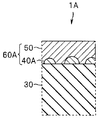
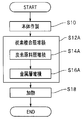
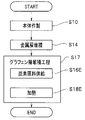
- 10 is a flowchart of a method for manufacturing a cantilever according to Modification 2. It is a fragmentary sectional view for demonstrating the manufacturing method of the cantilever of the modification 2. It is a fragmentary sectional view for demonstrating the manufacturing method of the cantilever of the modification 2. It is a fragmentary sectional view of the cantilever of the modification 2. 10 is a flowchart of a method for manufacturing a cantilever according to Modification 3. It is a fragmentary sectional view for demonstrating the manufacturing method of the cantilever of the modification 3.
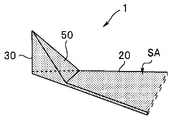
- FIG. 1 A sectional view of a cantilever 1 for a scanning probe microscope according to the present embodiment is shown in FIG. 1, and a partial perspective view is shown in FIG.
- the cantilever 1 includes a support portion 10, a lever portion 20, and a protrusion 30 that is a probe.
- the lever portion 20 that is a cantilever is extended from the support portion 10.
- the tetrahedral (triangular pyramid) shaped projection 30 is formed on the free end side of the lever portion 20, and the sharp tip of the projection 30 follows the fine irregularities on the nanoscale.
- the support part 10, the lever part 20, and the protrusion part 30 are produced by processing a silicon wafer.
- a graphene composite layer 60 which is a crystalline carbon composite layer, is deposited on the upper surface SA where the protrusions 30 are formed.
- the graphene composite layer 60 includes a metal layer 40 and a graphene layer 50 that is a crystalline carbon layer on the metal layer 40.
- the graphene layer 50 is composed of graphene, which is a crystalline carbon nanomaterial.
- the graphene referred to in this specification includes single-layer graphene having a thickness of about 0.3 nm and a plurality of single-layer graphene layers in which carbon atoms are two-dimensionally arranged in one layer. Is included.
- the thickness of the graphene layer 50 of the present embodiment is 1.5 nm, it is a multilayer graphene of 4 to 5 layers of single layer graphene.
- the metal material of the metal layer 40 is a catalyst used for forming the graphene layer 50 as described later. In other words, the metal material catalyzes the graphene formation reaction.
- the metal material is made of Sn.
- the thickness of the metal layer 40 is 3 nm. That is, the thickness of the graphene composite layer 60 composed of the graphene layer 50 and the metal layer 40 is 4.5 nm.
- the thickness is an arithmetic average value of thicknesses measured at a plurality of positions at the tip of the protrusion 30 using a transmission electron microscope (TEM). That is, the thickness of the layer refers to the thickness of the layer deposited on the tip portion of the protrusion 30.
- the curvature radius R was measured using a scanning electron microscope (SEM). Moreover, resistance value measured probe resistance with the atomic force microscope (AFM).
- the radius of curvature R of the tip portion on which the graphene composite layer 60 was coated was 8 nm.
- the probe resistance was about 1 M ⁇ , which was as low as when a 20 nm platinum layer was deposited.
- the crystalline carbon material refers to a carbon material in which 5 at% or more of the whole is crystallized, and may be a composite layer of graphene and another carbon crystal material.
- graphene may contain carbon nanofibers and carbon nanotubes.
- FIG. 3 shows a measurement state of a scanning capacitive microscope (SCM: Scanning Capacitance Microscope) using the cantilever 1.
- SCM scanning capacitive microscope
- the cantilever 1 is fixed to a jig 2 and a conducting wire 2A is electrically connected to the upper surface SA.
- the conducting wire 2A is connected to a detector 3 (Detector).
- Detector detector 3
- the electric capacity detected using cantilever 1 was substantially the same as that of cantilever 1 on which a 20 nm platinum layer was deposited.
- the ultrathin but low-resistance graphene layer 50 is deposited on the tip of the protrusion 30 by a non-transfer method including a low-temperature heat treatment instead of a transfer method. For this reason, manufacture is easy. Further, the cantilever 1 is a continuous film even though it is extremely thin, and a graphene layer having a low electrical resistance is deposited. Therefore, the radius of curvature R of the tip is 8 nm, and the radius of curvature R is deposited with a 20 nm platinum layer. Showed higher spatial resolution than 25 nm cantilevers. That is, the cantilever 1 has a low resistance and a high spatial resolution.
- the graphene layer 50 is excellent in chemical stability and wear resistance. For this reason, even if the cantilever 1 is used for a long period of time, it is less deteriorated than the conventional cantilever, has excellent durability, and can be used for a long period of time. In particular, when a biosample was measured, the tip was hardly soiled, so a stable image could be observed for a long time.
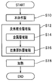
- Step S ⁇ Step S ⁇ b>10> Main Body Manufacturing Step
- a cantilever main body including the support portion 10, the lever portion 20, and the protruding portion 30 that is a probe is manufactured.
- the cantilever body is manufactured by processing a single crystal silicon wafer.
- the protrusion 30 is a tetrahedral type that includes two surfaces perpendicular to the upper surface of the lever portion 20 and a (111) surface having an angle of about 55 degrees.
- the lever part 20 and the protrusion part 30 of the cantilever main body may be made of a material different from silicon, for example, silicon nitride.
- the tip of the protrusion 30 may be sharpened by a known method, for example, FIB (Focus Ion Beam) method or low-temperature thermal oxidation treatment.
- FIB Fluorescence Ion Beam
- tip part of the cantilever main body of this embodiment was 5 nm.
- the carbon composite layer deposition step includes a metal layer deposition step and a carbon source layer deposition step of depositing the carbon source layer 51 on the metal layer 40.
- a metal layer 40 made of Sn was deposited in a thickness of 3 nm in a vacuum by a laser ablation method.
- the degree of vacuum was in the range of 1.0 ⁇ 10 ⁇ 5 Pa to 9.9 ⁇ 10 ⁇ 5 Pa, specifically in the range of 3 ⁇ 10 ⁇ 5 Pa to 7 ⁇ 10 ⁇ 5 Pa.
- a carbon raw material layer 51 made of amorphous carbon was deposited on the metal layer 40.
- the carbon source layer 51 was also deposited in a thickness of 1.5 nm in a vacuum by a laser ablation method.
- the degree of vacuum is the same as in the metal layer deposition process.
- Heating Step Heating was performed in vacuum at 250 ° C. for 1 hour, and then cooled to room temperature.
- the heating was controlled by mounting a cantilever on the substrate heating holder and based on the temperature of the heating holder. Since silicon has high thermal conductivity, the temperature of the heating holder can be regarded as the temperature of the cantilever.
- the degree of vacuum during heating is in the range of 1.0 ⁇ 10 ⁇ 4 Pa to 9.9 ⁇ 10 ⁇ 4 Pa, specifically, the range of 1 ⁇ 10 ⁇ 4 Pa to 7 ⁇ 10 ⁇ 4 Pa. It was in.
- the carbon composite layer 61 is a crystalline carbon composite layer made of a metal layer 40 and a graphene layer 50 that is crystalline carbon on the metal layer 40 by heat treatment, and has a thickness of 4.5 nm.
- the graphene composite layer 60 was changed.
- the radius of curvature R of the tip of the cantilever body before the carbon composite layer 61 is deposited is 5 nm
- the radius of curvature R of the cantilever 1 on which the crystalline carbon composite layer 60 is deposited is 8 nm. there were. That is, when the graphene composite layer 60 having a thickness of 4.5 nm is deposited, the radius of curvature R is increased by 4.5 nm in the calculation, but only 3 nm is actually increased. This is presumably because the thickness of the graphene composite layer 60 is thinner than 4.5 nm at the leading edge where the radius of curvature is measured.
- this sample was mounted on a substrate heating holder and heated in vacuum at 250 ° C. for 1 hour.
- the degree of vacuum during heating was in the range of 1.0 ⁇ 10 ⁇ 4 to 9.9 ⁇ 10 ⁇ 4 Pa, specifically, in the range of 1 ⁇ 10 ⁇ 4 Pa to 7 ⁇ 10 ⁇ 4 Pa. It was.
- the Raman spectroscopic analysis of the sample cooled to room temperature was performed. The results of this Raman spectroscopic analysis are shown in FIG.
- the thickness of the amorphous carbon layer was 5 nm, if all of the amorphous carbon is changed to graphene, the graphene layer is theoretically 16 to 17 layers. Further, since the same Raman spectrum was obtained on the entire surface of the substrate, it was confirmed that the graphene layer was formed on the entire surface of the substrate.
- the cantilever 1 can be used as a cantilever for measuring electrical characteristics.
- Electric Force Microscope EMF
- Scanning Capacitance Microscope SCM
- Scanning Kelvin Probe Microscope KPM
- Scanning Spreading Resistance Microscope SSRM
- electrostatic force microscope phase detection microscope
- SCFM scanning chemical force microscope
- SEcM scanning electrochemical microscope
- SCPM scanning chemical potential microscope
- SICM scanning ion conduction microscope
- the tetrahedral shape is shown as the shape of the protrusion 30 of the cantilever 1, but if the apex angle is an acute angle, it is a pyramidal or polygonal pyramid, or a conical protrusion. Similar effects can be obtained.
- the material of the protrusion 30 of the cantilever 1 does not need to be silicon, and may be, for example, silicon nitride, or may be a material different from that of the lever 20 or the support 10.
- the metal layer 40 of this embodiment should just contain at least any one of Zn, Sn, Bi, Pb, Tl, Cs, In, Cd, Rb, Ga, K, Na, Se, and Li. In particular, it is preferable to contain any of them as a main component.
- a main component means a 50 at% or more component.
- the metal layer 40 is any one of a single metal composed of one type of metal atom, a mixture of a plurality of metals composed of one type of metal atom, and an alloy composed of a plurality of types of metal atoms. Also good.
- the deposition method of the metal layer 40 various deposition methods for depositing a target material on the surface of the substrate can be employed.
- the deposition method include physical deposition methods such as sputtering, vapor deposition, laser ablation, inkjet, printing, spin coating, immersion, and chemical vapor deposition (CVD), and chemical deposition.
- the ink jet method is a method in which a target material is deposited on the surface of a substrate by ejecting droplets of a raw material liquid using an ink jet printer.
- the dipping method is a method in which a target material is deposited on the surface of the substrate by dipping the substrate in a raw material solution.
- the deposition atmosphere may be vacuum, inert gas atmosphere, or air.
- the deposition atmosphere when depositing by an inkjet method or a dipping method, the deposition atmosphere is air.
- the vacuum said in this specification means that it is the degree of vacuum of the pressure which is realizable with a vacuum pump.
- the degree of vacuum is preferably 1000 Pa or less, more preferably 10 Pa or less.
- amorphous carbon is shown as the carbon raw material layer 51, it is not limited to this, but silicon carbide (SiC), glassy carbon (gC), diamond-like carbon (DLC), amorphous carbon (a- C), titanium carbide (TiC), tungsten carbide (WC), chromium carbide (CrC), vanadium carbide (VC), or a layer containing a carbon element such as niobium carbide (NbC), the same effect Can be obtained. Further, the carbon source layer 51 may be deposited by a CVD method or the like.
- the carbon raw material layer 51 is not limited to being composed of only carbon atoms. Further, the carbon raw material layer 51 may be an organic material containing oxygen, hydrogen, nitrogen or the like instead of an inorganic material.
- the deposition method of the carbon raw material layer 51 various deposition methods for depositing a target material on the surface of the base material can be adopted as in the deposition method of the metal layer 40.
- the deposition atmosphere may be a vacuum, an inert gas atmosphere, or air, as in the method for forming the metal layer 40.
- the thickness of the metal layer 40 is preferably 0.1 nm or more, particularly preferably 1 nm or more. If the metal layer 40 is more than the said range, there will be a catalytic action. Moreover, if the thickness of the metal layer 40 is 7 nm or less, the spatial resolution of the cantilever can be ensured.
- the thickness of the carbon raw material layer 51 is preferably 0.3 nm or more and 7 nm or less. Since the thickness of the carbon raw material layer 51 is the thickness of the graphene layer 50, the conductivity can be ensured as long as it is not less than the above range. That is, the carbon raw material layer 51 having a thickness of 0.3 nm is a single-layer graphene layer 50, but conductivity is ensured.
- the curvature radius R of the tip can be made 10 nm or less. Can guarantee the spatial resolution of the cantilever.
- a nitrogen-doped graphene layer can be formed by heat treatment by depositing a raw material containing nitrogen and carbon, for example, a material containing melamine as a carbon raw material layer.
- a nitrogen-doped graphene layer in which nitrogen atoms replace carbon atoms of 0.1 at% to 20 at% is more excellent in conductivity than a pure graphene layer and can be preferably used for a cantilever.
- the electrical characteristics of the graphene layer can also be improved by doping with an element such as boron, fluorine, or chlorine.
- the carbon raw material layer 51 may contain atoms other than carbon and the catalyst metal, for example, oxygen, hydrogen, nitrogen, boron, fluorine, or chlorine.
- the catalyst metal for example, oxygen, hydrogen, nitrogen, boron, fluorine, or chlorine.
- nitrogen, fluorine, or chlorine is contained in the carbon raw material layer 51, a graphene layer with improved conductivity is formed by doping nitrogen, boron, fluorine, or chlorine by heat treatment.
- the metal layer 40 is made of a low melting point metal material. For this reason, the graphene layer is formed at a low temperature in the manufacturing method of the present embodiment as compared with the conventional graphene layer forming method using a metal catalyst.
- the heating temperature in the heating step may be not lower than the melting point temperature (MP) of the metal layer 40, but more preferably (MP + 10 ° C.) or higher.
- the upper limit of the heating temperature is 450 ° C. or less which does not damage the cantilever body made of silicon and / or silicon nitride.
- the heating temperature does not need to be significantly higher than the melting point temperature MP, and is preferably (MP + 30 ° C.) or less, for example.
- the lower limit of the heating temperature may be less than 300 ° C., for example, 250 ° C. or less, depending on the melting point MP of the metal layer.
- the lower limit of the melting point MP of the metal layer is not particularly limited, but is preferably room temperature or higher, particularly preferably 80 ° C. or higher, from the viewpoint of stability.
- the manufacturing method of the present embodiment is a transfer-free method, a graphene layer can be easily deposited on the tip of a small-diameter projection.
- a graphene layer can be obtained even when the heating temperature is equal to or lower than the melting point temperature MP of the metal layer 40.
- the heating temperature may be equal to or lower than the heat resistance temperature of the cantilever 1, but in order to minimize damage due to heat, a temperature slightly lower than the melting point MP of the metal material of the metal layer 40, for example, (MP-20 ° C. ) Or higher, and (MP-10 ° C.) or higher is particularly preferable.
- the heating temperature is 220 ° C. or higher, that is, (MP ⁇ 10) ° C. or higher, and 260 ° C. or lower, that is, (MP + 30 ° C.). Is particularly preferred.
- the heating temperature is particularly preferably 190 ° C. or higher and 230 ° C. or lower.
- the metal layer 40 preferably contains at least one of Sn, Zn, Bi, In, and Se in consideration of biosafety, ease of layer deposition, carbon solubility, cost, and the like. It is particularly preferable to use as a main component. Furthermore, the metal layer 40 preferably has a melting point MP of 80 ° C. or higher and 420 ° C. or lower.
- antimony (Sb) having a melting point MP of 631 ° C. cannot be used as the metal layer 40 of the present invention.
- a graphene layer may be formed by the manufacturing method of the present embodiment even for a metal that is said to be a non-solid solution system in which carbon does not dissolve, such as gallium (Ga). This is presumably because the metal forming the carbon solid solution contains impurities.
- the metal layer 40 is preferably made of a metal or alloy that forms a solid solution with carbon.
- the cantilever of the modified example of the embodiment and the manufacturing method of the cantilever of the modified example are similar to the cantilever 1 of the embodiment and have the same effect. Therefore, the same reference numerals are given to the components having the same function, and the description is omitted.
- the configuration / layer thickness of each layer, for example, the composition of the metal film is the same as that of the cantilever 1 of the embodiment.
- the structure of the metal layer 40A is not a continuous layer but an island shape (island shape).
- the metal layer tends to be island-shaped when it is thin.
- Sn tends to be island-shaped when the thickness is less than 3 nm.
- the thickness of the island-shaped metal layer 40A is an integrated average value. In other words, the thickness when the island-shaped metal layer 40A is melted to form a continuous film is regarded as the thickness of the island-shaped metal layer.
- a carbon source layer 51 having a thickness of 2 nm made of amorphous carbon is deposited on the island-shaped metal layer 40A made of Sn having a thickness of 2 nm.
- the carbon of the carbon raw material layer 51 is dissolved (dissolved) in the metal.
- an element having a small surface energy diffuses and separates into an upper layer.
- carbon has a lower surface energy than metal (Sn).
- the graphene layer 50 is formed so as to cover the metal layer 40 with the carbon that has been dissolved (dissolved) in the metal.
- the carbon raw material layer 51 that is not in direct contact with the metal material also changes to the graphene layer 50 by the heat treatment.
- the reason for this is not clear, but it is also considered that when the island-shaped metal layer 40A is heated and melted, a continuous film is formed.
- the cantilever 1A of this modification even if it is made thin, it can be used as a catalyst metal even if it is a metal material that tends to be in the shape of an island. Moreover, since the metal layer 40 with a thin average thickness is included, the cantilever 1A has a graphene composite layer thickness of 4 nm and a curvature radius R of the tip portion of 6 nm.
- a graphene layer that does not use the catalyst metal as a base at the most advanced portion of the protrusion 30.
- the metal material is not deposited on the foremost portion of less than 1 ⁇ m (for example, 500 nm) from the tip of the projection that affects the spatial resolution of the cantilever, the island-like metal material is deposited in a location exceeding 1 ⁇ m from the tip. If it is, a graphene layer can be arrange
- the carbon composite layer deposition step 12B includes a step of depositing a carbon source layer (S14B), and the metal layer is deposited on the carbon source layer. Step (S14B).
- a carbon raw material layer 51 made of amorphous carbon and having a thickness of 1.5 nm was deposited on the surface of the cantilever main body (protrusion 30).
- a metal layer 40 having a thickness of 3 nm made of Sn was deposited on the carbon raw material layer 51.
- the deposited metal layer 40 may have an island shape.
- the crystalline carbon composite layer 60B of the cantilever 1B changes to the metal layer 40 and the graphene layer 50 on the metal layer 40 in the same manner as the crystalline carbon composite layer 60 of the cantilever 1. To do.
- carbon has a smaller surface energy than metal (Sn). For this reason, as shown in FIG. 9C, it is presumed that the carbon that was dissolved (dissolved) in the metal in the heating step is deposited so as to cover the metal layer 40 to form the graphene layer 50.
- the carbon composite layer deposition step 12C is a step (S12B) in which a mixed layer in which a carbon raw material and a metal material are mixed is deposited.
- a 5 nm thick mixed layer 63 composed of 50 at% amorphous carbon and 50 at% Sn was deposited on the surface of the cantilever main body (protrusion 30).
- the mixed layer 63 was changed to the crystalline carbon composite layer 60 shown in FIG. 11B by heat treatment (250 ° C.).
- the Sn content of the mixed layer 63 can be in the range of 1 at% to 99 at% of the whole.
- the crystalline carbon composite layer may have the same configuration as that of the cantilever 1D, that is, a metal inclusion structure.
- a graphene layer deposition step S17 is performed in which the carbon material supply step (S16E) and the heating step (S18E) are performed simultaneously.
- a metal layer 40 made of Sn and having a thickness of 1.5 nm was deposited on the surface of the cantilever main body (protrusion 30).
- heating is performed while supplying a carbon source gas containing carbon atoms. Heating may be performed in vacuum, in an inert gas atmosphere, in a reducing atmosphere such as hydrogen, or in the air.
- the metal layer may have an island shape as in the cantilever 1A of the first modification.
- the method further includes the step of removing the metal layer 40 after the heating step for changing the carbon composite layer to a crystalline carbon composite layer containing a metal material and crystalline carbon. It may be.
- the metal layer removing process is, for example, an additional heating process at the same temperature as the heating process and a processing time that is twice or more that of the heating process, an additional heating process at a higher temperature than the heating process, or an etching process.
- the metal material constituting the metal layer by the additional heating process evaporates when the heating temperature is equal to or higher than the melting point MP, and sublimates and disappears when the heating temperature is equal to or lower than the melting point.
- a part of the metal layer 40F under the graphene layer (crystalline carbon layer) 50 is a cavity 40X.
- the metal layer disappears, and a part of the graphene layer (crystalline carbon layer 60G) 50G becomes a cavity 40X.
- the metal layer removal process makes it seem that the graphene layer is directly deposited on the substrate.
- the cantilever from which the metal layer has been removed exhibits a higher spatial resolution because the radius of curvature R of the tip is smaller.
- a conductive metal layer 70 made of aluminum having a thickness of 0.2 ⁇ m is deposited on the root portion, the lever portion, and the support portion of the protruding portion 30.
- the cantilever 1H is manufactured by covering the entire surface of the cantilever with an aluminum layer after depositing the graphene layer 50 and then selectively removing the aluminum layer at the tip.
- the cantilever 1H has the same spatial resolution as the cantilever 1 and the like, and has a lower electrical resistance.
- the thickness of the conductive metal layer 70 is preferably 1 ⁇ m or less, and particularly preferably 0.3 ⁇ m or less.
- the graphene composite layer 60 including the graphene layer 50 and the metal layer 40 may be deposited only on the tip of the protrusion 30 as in the cantilever 1I of the modified example 9 illustrated in FIG. 15B. No. In the cantilever 1I, the conductive metal layer 70 is deposited after the graphene composite layer 60 is deposited. On the other hand, the graphene composite layer 60 may be deposited after the conductive metal layer 70 is deposited.
- a carbon raw material layer 51 having a thickness of 1.5 nm made of amorphous carbon was deposited on the surface of the cantilever main body (projecting portion 30). Further, a 3 nm-thick metal layer 40 made of In (indium) was deposited on the carbon source layer 51. That is, the carbon composite layer 62 includes the carbon raw material layer 51 and the metal layer 40 on the carbon raw material layer 51.
- the carbon composite layer 62 includes the metal layer 40, the first graphene layer 50A above the metal layer 40, and the second graphene layer 50B below the metal layer 40. It changed into the crystalline carbon composite layer 60J.
- the melting point (MP) of indium is 157 ° C. Therefore, in the heating process at 170 ° C., indium is melted, carbon dissolved in the molten indium is diffused, and re-deposited on the metal layer 40 as the first graphene layer 50A.
- the crystalline carbon composite layer 62 is composed of the metal layer 40 and the first graphene layer on the metal layer 40. 50A and the second graphene layer 50B under the metal layer 40.
- an alloy material having a melting point lower than that of the main component metal may be used as the metal layer 40.
- the melting point of the SnIn alloy is lower than the melting point of Sn (230 ° C.) and the melting point of In (157 ° C.), for example, 117 ° C.
- a cantilever having a low melting point metal layer 40 can be produced by a heat treatment at a lower temperature.
- a cantilever having a metal layer with a melting point MP of 117 ° C. can be produced at 97 ° C. (MP ⁇ 20 ° C.) of 100 ° C. or less.
- the method for manufacturing the cantilever 1 ⁇ / b> K of Modification 11 further includes a step of removing the metal layer 40 (Step S ⁇ b> 19).
- a carbon raw material layer 51 made of amorphous carbon and having a thickness of 10 nm was deposited on the surface of the cantilever main body (protrusion 30). Further, a 50 nm thick metal layer 40 made of an In—Sn alloy having a melting point MP of 120 ° C. was deposited on the carbon source layer 51. That is, the carbon composite layer 62 includes the carbon raw material layer 51 and the metal layer 40 on the carbon raw material layer 51.
- the carbon composite layer 62 is subjected to heat treatment, like the crystalline carbon composite layer 62 shown in FIG. 16B, the metal layer 40, the first graphene layer 50 ⁇ / b> A on the metal layer 40, and the bottom of the metal layer 40. Changes to the second graphene layer 50B
- step S19 the process (step S19) of removing the metal layer 40 was performed after the heating process (step S18). That is, the metal layer 40 and the first graphene layer 50A were removed by a chemical etching process using an acidic solution (10 wt% nitric acid). The first graphene layer 50A is not dissolved in the acidic solution. However, when the metal layer 40 is dissolved by the chemical etching process, the first graphene layer 50A thereon is also peeled from the cantilever.
- the second graphene layer 50B is deposited on the tip of the cantilever 1K.
- the thickness of the second graphene layer 50B was 2 nm, and the radius of curvature R at the tip was 6 nm. That is, the thickness of the second graphene layer 50B is thinner than the thickness of the first graphene layer 50A estimated to be 8 nm. Then, the thick first graphene layer 50A and the metal layer 40 are removed, and only the thin second graphene layer 50B remains at the tip of the cantilever 1K.
- a cantilever having substantially the same structure as that of the cantilever 1K was produced even when heating was performed in a vacuum at 130 ° C. for 0.5 hour.
- the second graphene layer 50B may be deposited only on the tip of the protrusion 30.
- the manufacturing method of the cantilever manufactured by the manufacturing method of the present invention it is very difficult for the cantilever 1K of the modification 11 shown in FIG. 18 to prove that the first metal layer 50A and the first graphene layer 50A are removed in the metal layer removal step (S19). It is.
- the cantilever manufactured by the method for manufacturing a cantilever of the present invention may be different in the state of the interface between the substrate and the graphene layer from the cantilever manufactured by the conventional manufacturing method.
- the structure of the interface for example, the crystal structure can be analyzed using a transmission electron microscope or the like, the manufacturing method cannot be verified from the structure.
- the temperature of the heating process is 450 ° C. or lower. That is, the cantilever manufactured by the method for manufacturing a cantilever of the present invention cannot find a word specifying a structure or a characteristic related to a difference from the prior art, and is analyzed and specified based on the measurement. It is impossible or impractical to do.
Landscapes
- Physics & Mathematics (AREA)
- Health & Medical Sciences (AREA)
- General Health & Medical Sciences (AREA)
- General Physics & Mathematics (AREA)
- Nuclear Medicine, Radiotherapy & Molecular Imaging (AREA)
- Radiology & Medical Imaging (AREA)
- Chemical & Material Sciences (AREA)
- Engineering & Computer Science (AREA)
- Nanotechnology (AREA)
- Chemical Kinetics & Catalysis (AREA)
- General Chemical & Material Sciences (AREA)
- Carbon And Carbon Compounds (AREA)
Abstract
走査型プローブ顕微鏡に用いられるカンチレバー1は、支持部10とレバー部20と探針である突起部30とを含み、突起部30の先端部に、結晶性炭素ナノ材料と融点MPが420℃以下の金属材料とを含む結晶性炭素複合層60が、堆積されている
Description
本発明は、走査型プローブ顕微鏡に用いられるカンチレバーおよび前記カンチレバーの製造方法に関する。
走査型プローブ顕微鏡(SPM:Scanning Probe Microscope)は、試料表面の形状を高分解能で検出するのに適しており、半導体、光ディスク、又はバイオ試料等の表面形状の測定に利用されている。ナノスケールの微細構造を検出するために、SPMに用いられるカンチレバーの突起部の先端部は尖鋭である。
各種の電気特性測定を行うためには、シリコン等からなるカンチレバーは、導電金属、例えば、白金からなる金属層が堆積され、導電化される。
カンチレバーは表面に金属層が堆積されると、突起部の先端部も、金属層の厚さの分だけ太くなり先端が微細な凹部の底まで届かなくなるおそれがある。すなわち、カンチレバーは金属層の堆積により先端部の曲率半径Rが増加すると、空間分解能が低下する。このため、導電化のための金属層の厚さは、より薄いことが好ましい。
しかし、金属層は厚さ(平均厚さ)が薄いと、その構造は連続層ではなく、アイランド状(島状)になりやすい。島と島とは導通状態ではないため、薄い金属層では、カンチレバーの表面を十分に導電化することはできない。十分に導電化するために、例えば、先端部の曲率半径Rが、5nmのカンチレバー表面に20nmの白金層を堆積すると、先端部の曲率半径Rは25nmに増加する。
中国特許出願公開第102353817号明細書および国際公開第2014/090938号には、表面にグラフェン層を堆積したカンチレバーが開示されている。グラフェン層は、単層であっても、電子移動度が非常に高く、カンチレバーの導電層として好適である。
中国特許出願公開第102353817号明細書に開示されているカンチレバーでは、Ni層の上に1層から数層のグラフェン層がCVD法により堆積されている。
上記明細書には詳細は開示されていないが、Niを金属触媒とするグラフェン層の製造方法では、メタン等の炭化水素を1000℃程度に加熱して反応する熱化学気相合成法が用いられることは当業者にとり周知である。
また、日本国特開2013-98396号公報には、ケイ素を含む炭素化合物層を加熱する無転写法によるグラフェンの製造方法が開示されている。この方法では、1200℃以上の加熱によりケイ素が触媒となり、炭素化合物がグラフェンに変化する。
日本国特許第4970619号明細書には、アモルファスカーボン膜とガリウム(Ga)とを接触させ、接触界面にグラフェン膜を形成する工程を含むグラフェン膜の製造方法が記載されている。
さらに、ガリウムと同様の性質に基づき、インジウム(In)、スズ(Sn)およびアンチモン(Sb)にも、同様の効果が類推されると記載されている。
上記明細書によれば、冶金学的には、ガリウムと炭素とは全率非固溶である。しかし、真空中、約1000℃程度の熱処理中に、固体の炭素原子と液体のガリウム原子との界面に原子結合が形成されるため、アモルファスカーボン膜がグラフェン膜に変化すると考えられている。
すなわち、従来の無転写法または原子結合法によるグラフェン堆積法では、少なくとも1000℃程度の高温加熱が不可欠であるため、カンチレバーが変形し歩留まりが低下するおそれがあった。
一方、国際公開第2014/090938号に開示されているカンチレバーは、ポリメタクリル酸メチル(PMMA)の薄層を中間層として、別途、作製されたグラフェンシートを接着する、いわゆる転写法により製造されている。
また、日本国特許第5705315号明細書には、金属触媒層を含むロール変形する基材上に500℃以下で、グラフェン層を形成した後にグラフェン層を転写するロールツーロール工程が記載されている。
しかし、カンチレバーの先端部にグラフェンシートを均一に転写(接着)するのは容易ではない。さらに、中間層の厚さにより、カンチレバーの空間分解能(解像度)が低下するおそれがあった。
本発明の実施形態は、低抵抗で、かつ、空間分解能が高いカンチレバーを提供することを目的とする。
本発明の別の実施形態は、低抵抗で、かつ、空間分解能が高いカンチレバーの製造方法を提供することを目的とする。
本発明の実施形態のカンチレバーは、走査型プローブ顕微鏡に用いられる、支持部とレバー部と探針である突起部とを含むカンチレバーであって、前記突起部の先端部に、結晶性炭素ナノ材料と融点MPが420℃以下の金属材料とを含む結晶性炭素複合層が、堆積されている。
本発明の別の実施形態のカンチレバーの製造方法は、支持部とレバー部と探針である突起部とを含むカンチレバー本体の前記突起部の先端部に、結晶性炭素ナノ材料からなる結晶性炭素層が堆積されているカンチレバーの製造方法であって、前記カンチレバー本体が作製される工程と、前記突起部の前記先端部に、融点MPが420℃以下の金属材料と炭素原料とを含む炭素複合層が堆積される炭素複合層堆積工程と、温度が450℃以下の加熱工程と、を具備する。
本発明の実施形態によれば、低抵抗で、かつ、空間分解能が高いカンチレバーが提供できる。
本発明の別の実施形態によれば、低抵抗で、かつ、空間分解能が高いカンチレバーの製造方法を提供できる。
<実施形態>
<カンチレバーの構造>
本実施形態の走査型プローブ顕微鏡用のカンチレバー1の断面図を図1に、部分斜視図を図2に示す。
<カンチレバーの構造>
本実施形態の走査型プローブ顕微鏡用のカンチレバー1の断面図を図1に、部分斜視図を図2に示す。
なお、以下の説明において、各実施形態に基づく図面は、模式的なものであり、各部分の厚みと幅との関係、夫々の部分の厚みの比率などは現実のものとは異なることに留意すべきであり、図面の相互間においても互いの寸法の関係や比率が異なる部分が含まれている場合がある。また、一部の構成要素の図示、符号の付与は省略する場合がある。
カンチレバー1は、支持部10とレバー部20と探針である突起部30とを含む。片持ち梁であるレバー部20は支持部10から延設されている。テトラヘドラル(三角錐)形状の突起部30は、レバー部20の自由端側に形成されている、突起部30の尖鋭な先端部は、ナノスケールの微細な凹凸に追従する。
支持部10とレバー部20と突起部30とはシリコンウエハを加工して作製されている。
そして、カンチレバー1では、突起部30が形成されている上面SAに、結晶性炭素複合層であるグラフェン複合層60が堆積されている。グラフェン複合層60は、金属層40と、金属層40の上の結晶性炭素層であるグラフェン層50とからなる。
グラフェン層50は、結晶性炭素ナノ材料であるグラフェンで構成されている。本明細書でいうグラフェンには、炭素原子が二次元的に配列している層が1層である、厚さ約0.3nmの単層グラフェンおよび複数の単層グラフェンが積層されている多層グラフェンが含まれる。
なお後述するように、本実施形態のグラフェン層50の厚さは、1.5nmであるので、単層グラフェン4~5層の多層グラフェンである。
また、金属層40の金属材料は、後述するように、グラフェン層50を形成するために用いられる触媒である。換言すると、金属材料は、グラフェンの形成反応に対して触媒作用を果たす。本実施形態では、金属材料はSnからなる。そして、金属層40の厚さは3nmである。すなわち、グラフェン層50と金属層40とからなるグラフェン複合層60の厚さは、4.5nmである。
なお、厚さは、突起部30の先端部の複数箇所を、透過型電子顕微鏡(TEM)を用いて測定した厚さの算術平均値である。すなわち、層の厚さは、突起部30の先端部に堆積された層の厚さをいう。また曲率半径Rは、走査型電子顕微鏡(SEM)を用いて測定した。また、抵抗値は原子間力顕微鏡(AFM)によりプローブ抵抗を測定した。
そして、カンチレバー1では、グラフェン複合層60がコーティングされている先端部の曲率半径Rは、8nmであった。また、プローブ抵抗は1MΩ程度であり、20nmの白金層を堆積した場合と同等の低抵抗であった。
なお、以上の説明では結晶性炭素材料がグラフェンの場合について説明した。しかし、結晶性炭素材料としては、全体の5at%以上が結晶化している炭素材料をいい、グラフェンと他の炭素結晶材料との複合層であってもよい。例えばグラフェンが、カーボンナノファイバ、カーボンナノチューブを含んでいてもよい。
図3にカンチレバー1を用いた、走査型容量顕微鏡(SCM:Scanning Capacitance Microscope)の測定状態を示す。カンチレバー1は、治具2に固定され、上面SAに導線2Aが電気的に接続される。導線2Aは検出部(Detector)3と接続されている。カンチレバー1の突起部の先端が試料4と接することで、試料4の表面の局所的な電気容量が検出される。
カンチレバー1を用いて検出された電気容量は、20nmの白金層を堆積したカンチレバー1と略同じであった。
以上の説明のように、カンチレバー1は、極薄でも低抵抗のグラフェン層50が、転写法ではなく、低温の熱処理を含む非転写法により突起部30の先端部に堆積されている。このため製造が容易である。さらに、カンチレバー1には、極薄でも連続膜となり、かつ、電気抵抗の低いグラフェン層が堆積されているため、先端部の曲率半径Rが8nmであり、20nmの白金層を堆積した曲率半径Rが25nmのカンチレバーよりも高い空間分解能を示した。すなわち、カンチレバー1は、低抵抗で、かつ、空間分解能が高い。
また、グラフェン層50は、化学的安定性および耐磨耗性が優れている。このため、カンチレバー1は、長期間使用しても、従来のカンチレバーよりも劣化が小さく、耐久性が優れており、長期間の使用が可能であった。特に、バイオ試料を測定した場合には、先端に汚れがつきにくく、そのため安定した像が長時間観察できた。
<カンチレバーの製造方法>
次に、図4のフローチャートに沿って、カンチレバー1の製造方法を説明する。
次に、図4のフローチャートに沿って、カンチレバー1の製造方法を説明する。
<ステップS10>本体作製工程
支持部10とレバー部20と探針である突起部30とを含むカンチレバー本体が作製される。カンチレバー本体は、単結晶シリコンウエハを加工して作製される。突起部30はレバー部20の上面に対して垂直な2面と、角度約55度の(111)面と、からなる、テトラヘドラル型である。
支持部10とレバー部20と探針である突起部30とを含むカンチレバー本体が作製される。カンチレバー本体は、単結晶シリコンウエハを加工して作製される。突起部30はレバー部20の上面に対して垂直な2面と、角度約55度の(111)面と、からなる、テトラヘドラル型である。
カンチレバー本体のレバー部20と突起部30がシリコンとは別の材料、例えば、窒化シリコンで構成されていてもよい。
また、なお、突起部30の先端が、公知の方法、例えば、FIB(Focus Ion Beam)法または低温熱酸化処理により尖鋭化されていてもよい。なお、本実施形態のカンチレバー本体の先端部の曲率半径Rは、5nmであった。
<ステップS12>炭素複合層堆積工程
カンチレバー本体の表面に金属材料と炭素原料とを含む炭素複合層61が堆積される。本実施形態の製造方法では、炭素複合層堆積工程は、金属層堆積工程と、金属層40の上に炭素原料層51を堆積する炭素原料層堆積工程とからなる。
カンチレバー本体の表面に金属材料と炭素原料とを含む炭素複合層61が堆積される。本実施形態の製造方法では、炭素複合層堆積工程は、金属層堆積工程と、金属層40の上に炭素原料層51を堆積する炭素原料層堆積工程とからなる。
<ステップS14>金属層堆積工程
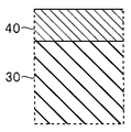
図5Aに示すように、Snからなる金属層40をカンチレバー本体(突起部30)の表面に堆積させた。図5A等は、突起部30の先端部の部分断面図であるが、金属層40は支持部10とレバー部20にも堆積された。
図5Aに示すように、Snからなる金属層40をカンチレバー本体(突起部30)の表面に堆積させた。図5A等は、突起部30の先端部の部分断面図であるが、金属層40は支持部10とレバー部20にも堆積された。
すなわち、レーザアブレーション法により真空中で、Snで構成される金属層40を3nm堆積させた。真空度は、1.0×10⁻⁵Pa~9.9×10⁻⁵Paの範囲内、具体的には、3×10⁻⁵Pa~7×10⁻⁵Paの範囲内であった。
<ステップS16>炭素原料層堆積工程
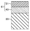
図5Bに示すように、金属層40の上に非晶質炭素からなる炭素原料層51を堆積させた。炭素原料層51も、レーザアブレーション法により真空中で1.5nm堆積させた。真空度は金属層堆積工程と同じである。
図5Bに示すように、金属層40の上に非晶質炭素からなる炭素原料層51を堆積させた。炭素原料層51も、レーザアブレーション法により真空中で1.5nm堆積させた。真空度は金属層堆積工程と同じである。
<ステップS18>加熱工程
真空中で250℃、1時間の加熱を行い、その後、室温まで冷却した。加熱は、基板加熱ホルダーにカンチレバーを装着し、加熱ホルダーの温度をもとに制御を行った。シリコンは熱伝導率が高いため、加熱ホルダーの温度をカンチレバーの温度と見なすことができる。なお、加熱時の真空度は、1.0×10⁻⁴Pa~9.9×10⁻⁴Paの範囲内、具体的には、1×10⁻⁴Pa~7×10⁻⁴Paの範囲内であった。
真空中で250℃、1時間の加熱を行い、その後、室温まで冷却した。加熱は、基板加熱ホルダーにカンチレバーを装着し、加熱ホルダーの温度をもとに制御を行った。シリコンは熱伝導率が高いため、加熱ホルダーの温度をカンチレバーの温度と見なすことができる。なお、加熱時の真空度は、1.0×10⁻⁴Pa~9.9×10⁻⁴Paの範囲内、具体的には、1×10⁻⁴Pa~7×10⁻⁴Paの範囲内であった。
図5Cに示すように加熱処理により炭素複合層61は、金属層40と金属層40の上の結晶性炭素であるグラフェン層50とからなる結晶性炭素複合層である、厚さ4.5nmのグラフェン複合層60に変化した。
そして、すでに説明したように、炭素複合層61を堆積する前のカンチレバー本体の先端部の曲率半径Rは5nmで、結晶性炭素複合層60が堆積されたカンチレバー1の曲率半径Rは、8nmであった。すなわち、厚さ4.5nmのグラフェン複合層60を堆積すると、計算上では曲率半径Rは4.5nm増加するが、実際には3nmしか増加していなかった。この原因は曲率半径を測定している最先端部ではグラフェン複合層60の厚さが、4.5nmよりも薄いためと推定される。
なお、炭素複合層61が加熱により、グラフェン複合層60に変化したことは、電気抵抗の測定結果および透過電子顕微鏡観察から明らかである。しかし、念のため、別途、作製した試料でも確認した。すなわち、熱酸化シリコン(SiO2)基板上に、レーザアブレーション法により真空中で、Snで構成される金属層を15nm堆積させた。さらに、金属層の上に、レーザアブレーション法により真空中で、非晶質炭素層を5nm堆積させた。何れの層の堆積時も、真空度は、1.0×10⁻⁵Pa~9.9×10⁻⁵Paの範囲内、具体的には、3×10⁻⁵Pa~7×10⁻⁵Paの範囲内であった。その後、この試料を基板加熱ホルダー上に装着し、真空中で250℃、1時間の加熱を行った。加熱時の真空度は、1.0×10⁻⁴~9.9×10⁻⁴Paの範囲内、具体的には、1×10⁻⁴Pa~7×10⁻⁴Paの範囲内であった。その後、室温まで冷却された試料のラマン分光分析を行った。このラマン分光分析結果を図6に示す。
図6に示すように、基板のSiO2(519cm-1)に由来するピークの他に、グラフェンの形成を示す2D(2713cm-1)ピーク、グラファイト化を示すG(1584cm-1)ピーク、欠陥に由来するD(1352cm-1)ピークが確認できる。2Dピークが確認されており、DピークがGピークに比べて非常に小さい(IG/ID=3.37)ことから、欠陥の少ない高品質のグラフェン層が形成されていることが分かる。また、2DピークとGピークとの強度比(I2D/IG=0.54)から、グラフェン層は3層以上の複数層からなる多層グラフェン層であることが分かる。なお、非晶質炭素層の厚さは5nmであったため、非晶質炭素がすべてグラフェンに変化すれば、理論的にはグラフェン層は16~17層となる。また、基板上の全面で、同様のラマンスペクトルが得られたことから、グラフェン層は基板全面に形成されていることが確認された。
カンチレバー1は、電気特性測定用のカンチレバーとして用いることができる。例えば、電気力顕微鏡(EFM:Electric Force Microscope)、走査型容量顕微鏡(SCM:Scanning Capacitance Microscope)、走査型ケルビンプローブ顕微鏡(KPM:Kelvin Probe force Microscopy)、走査型広がり抵抗顕微鏡(SSRM:Scanning Spreading Resistance Microscope)、静電力顕微鏡、位相検波顕微鏡(PDM)、走査型化学力顕微鏡(SCFM)、走査型電気化学顕微鏡(SEcM)、走査型化学ポテンシャル顕微鏡(SCPM)、走査型イオン伝導顕微鏡(SICM)及びナノ電位差測定を含む電気特性測定用として用いることができる。
なお、本実施形態では、カンチレバー1の突起部30の形状としてテトラヘドラル形状を示したが、頂角が鋭角であれば、ピラミダル形状もしくは多角形形状の角錐状、または円錐状の突起部であれば同様な効果が得られる。また、カンチレバー1の突起部30の材料は、シリコンである必要はなく、例えば、窒化シリコンでもよいし、さらに、レバー部20または支持部10と別の材料であってもよい。
そして、本実施形態の金属層40は、Zn、Sn、Bi、Pb、Tl、Cs、In、Cd、Rb、Ga、K、Na、Se、および、Liの少なくともいずれかを含んでいればよく、特に、いずれかを主成分として含んでいることが好ましい。なお、主成分とは、50at%以上の成分をいう。金属層40は、1種類の金属原子で構成された単体の金属、1種類の金属原子で構成された金属が複数混合された混合物、複数種類の金属原子で構成された合金のいずれであってもよい。
金属層40の堆積方法としては、基材の表面上に目的の材料を堆積させる種々の堆積方法が採用可能である。堆積方法としては、スパッタ法、蒸着法、レーザアブレーション法、インクジェット法、印刷法、スピンコート法、浸漬法、化学気相合成法(CVD法)などの物理堆積法および化学堆積法が挙げられる。インクジェット法は、インクジェットプリンターを用いて、原料液の液滴を飛ばして、基材の表面に目的の材料を堆積させる方法である。浸漬法は、原料液に基材を浸漬して、基材の表面上に目的の材料を堆積させる方法である。
堆積雰囲気は、真空、不活性ガス雰囲気、大気のいずれでもよい。例えば、インクジェット法、または浸漬法で堆積させる場合、堆積雰囲気は大気である。なお、本明細書で言う真空とは、真空ポンプで実現可能な程度の圧力の真空度であることを意味する。真空中で堆積させる場合、1000Pa以下の真空度とすることが好ましく、10Pa以下の真空度とすることがより好ましい。
一方、炭素原料層51として、非晶質炭素を示したが、これに限定されず、シリコンカーバイト(SiC)、グラッシーカーボン(g-C)、ダイヤモンドライクカーボン(DLC)、アモルファスカーボン(a-C)、炭化チタン(TiC)、タングステンカーバイト(WC)、クロムカーバイト(CrC)、バナジウムカーバイト(VC)またはニオブカーバイト(NbC)等の炭素元素を含む層であれば、同様な効果を得ることができる。更に、炭素原料層51の堆積方法は、CVD法等でもよい。
すなわち、炭素原料層51は、炭素原子のみで構成されている場合に限られない。さらに、炭素原料層51は、無機物ではなく、酸素、水素、窒素等を含んでいる有機物であってもよい。炭素原料層51の堆積方法としては、金属層40の堆積方法と同様に、基材の表面上に目的の材料を堆積させる種々の堆積方法が採用可能である。堆積雰囲気は、金属層40の形成方法と同様に、真空、不活性ガス雰囲気、または大気のいずれでもよい。
金属層40の厚さは、0.1nm以上が好ましく、1nm以上が特に好ましい。金属層40は前記範囲以上であれば、触媒作用を奏する。また、金属層40の厚さは、7nm以下であれば、カンチレバーの空間分解能を担保できる。
炭素原料層51の厚さは、0.3nm以上7nm以下が好ましい。炭素原料層51の厚さは、グラフェン層50の厚さとなるため、前記範囲以上であれば、導電性を担保できる。すなわち、厚さ0.3nmの炭素原料層51は、単層グラフェン層50であるが、導電性は担保されている。
また、金属層40の厚さと炭素原料層51の厚さとの合計の厚さ、すなわち、炭素複合層61の厚さが、7nm以下であれば、先端部の曲率半径Rを10nm以下にできるため、カンチレバーの空間分解能を担保できる。
なお、窒素および炭素を含む原料、例えば、メラミン含む材料を炭素原料層として堆積しておくことで、加熱処理により窒素がドープされたグラフェン層を形成できる。窒素原子が、0.1at%~20at%の炭素原子を置換している窒素ドープグラフェン層は、純粋なグラフェン層よりも導電性に優れているため、カンチレバーに好ましく用いることができる。ホウ素、フッ素、または塩素等の元素をドープすることでも、グラフェン層の電気特性を向上することができる。
すなわち、炭素原料層51は、炭素および触媒金属以外の原子、例えば、酸素、水素、窒素、ホウ素、フッ素、または塩素を含んでいてもよい。特に、炭素原料層51に窒素、フッ素または塩素が含まれる場合加熱処理により、窒素、ホウ素、フッ素または塩素がドープされ、導電性が向上したグラフェン層が形成される。
本実施形態の製造方法では、触媒である金属材料が加熱によって溶融し液体化した金属材料に炭素原子が溶解すると考えられる。そして、金属材料に溶解していた炭素原子が拡散し、金属層の表面に析出し規則的に配列することで、グラフェン層50が形成される。
炭素原子の溶解量および拡散速度は、金属が固体から液体に変化すると大幅に増加する。金属層40は低融点金属材料からなる。このため、従来の金属触媒によるグラフェン層形成法と比べて本実施形態の製造方法では、低温でグラフェン層が形成される。
加熱工程の加熱温度は、金属層40の融点温度(MP)以上であればよいが、(MP+10℃)以上がより好ましい。加熱温度の上限は、シリコンまたは/および窒化シリコンからなるカンチレバー本体を損傷することのない450℃以下である。加熱温度は、融点温度MPより大幅に高温にする必要はなく、例えば(MP+30℃)以下であることが好ましい。
加熱温度の下限は、金属層の融点MPに応じて、300℃未満でもよく、例えば250℃以下でもよい。なお、金属層の融点MPの下限は、特に制限はないが、安定性の観点から、室温以上が好ましく、特に好ましくは80℃以上である。さらに本実施形態の製造方法は無転写法のため、細径の突起部の先端部にも簡単にグラフェン層を堆積できる。
なお、金属材料は溶融していなくとも、融点MPより僅かに低い温度まで加熱されると、炭素原子の拡散速度は、大幅に増加する。
このため、加熱温度が金属層40の融点温度MP以下でもグラフェン層が得られる。加熱温度は、カンチレバー1の耐熱温度以下であればよいが、熱による損傷を最小限とするためには、金属層40の金属材料の融点MPより僅かに低い温度、例えば、(MP-20℃)以上が好ましく、(MP-10℃)以上が特に好ましい。
例えば、金属層40の金属材料として、Sn(MP=230℃)を用いた場合には、加熱温度は220℃以上、すなわち(MP-10)℃以上、260℃以下、すなわち、(MP+30℃)が特に好ましい。同様に、金属材料としてSn-3at%Ag-3at%Bi-3at%In合金(MP=200℃)を用いた場合には、加熱温度は190℃以上230℃以下が特に好ましい。同様に、金属層としてZn(MP=420℃)を用いた場合には、加熱温度は410℃以上450℃以下が特に好ましい。
すなわち、Zn(MP=420℃)、Sn(MP=230℃)、Bi(MP=271℃)、Pb(MP=328℃)、Tl(MP=304℃)、Cs(MP=29℃)、In(MP=157℃)、Cd(MP=321℃)、Rb(MP=38.5℃)、Ga(MP=30℃)、K(MP=64℃)、Na(MP=98℃)、Se(MP=217℃)、および、Li(MP=179℃)のいずれかの元素を主成分として含む金属で構成されている金属層40を有するカンチレバーの製造方法は低温プロセスである。
金属層40は、生体安全性、層堆積の容易性、炭素の溶解度、およびコスト等を考慮すると、Sn、Zn、Bi、In、およびSeの少なくともいずれかを含んでいることが好ましく、いずれかを主成分とすることが特に好ましい。さらに、金属層40は、融点MPが、80℃以上420℃以下であることが好ましい。
例えば、融点MPが、631℃のアンチモン(Sb)は、本発明の金属層40として用いることは出来ない。
なお、炭素が溶解しない全率非固溶系と言われている金属、例えば、ガリウム(Ga)であっても、本実施形態の製造方法によりグラフェン層が形成されることがある。これは、炭素固溶体を形成する金属が不純物として含まれているためと推定される。
しかし、金属層40が、炭素と固溶体を形成する金属または合金からなることが好ましいことは言うまでも無い。
<実施形態の変形例>
実施形態の変形例のカンチレバーおよび変形例のカンチレバーの製造方法は、実施形態のカンチレバー1等と類似し同じ効果を有するため、同じ機能の構成要素には同じ符号を付し説明は省略する。なお、各層の構成/層厚等、例えば、金属膜の組成は、実施形態のカンチレバー1等と同じである。
実施形態の変形例のカンチレバーおよび変形例のカンチレバーの製造方法は、実施形態のカンチレバー1等と類似し同じ効果を有するため、同じ機能の構成要素には同じ符号を付し説明は省略する。なお、各層の構成/層厚等、例えば、金属膜の組成は、実施形態のカンチレバー1等と同じである。
<変形例1>
図7Aに示すように、本変形例のカンチレバー1Aの製造方法では、金属層40Aの構造は連続層ではなく、アイランド状(島状)である。
図7Aに示すように、本変形例のカンチレバー1Aの製造方法では、金属層40Aの構造は連続層ではなく、アイランド状(島状)である。
すなわち、金属層は、その材料(元素)の種類によっては、厚さが薄い場合に島状となりやすい。例えば、Snでは、厚さが3nm未満では島状となりやすい。なお、島状の金属層40Aの厚さは、積分平均値とする。言い替えれば、島状の金属層40Aが溶融して連続膜となったときの厚さを島状の金属層の厚さとみなす。
そして、図7Bに示すように、Snからなる厚さ2nmのアイランド状の金属層40Aの上に、非晶質炭素からなる厚さ2nmの炭素原料層51が堆積される。
加熱工程において炭素原料層51の炭素は金属に固溶(溶解)する。一般に、A/B積層体が加熱され固溶すると、表面エネルギーが小さい元素が拡散し、上の層になるように分離する。本変形例の場合、炭素は金属(Sn)に比べて表面エネルギーが小さい。このため、図7Cに示すように、金属に固溶(溶解)していた炭素は金属層40を覆うようにグラフェン層50を形成する。
すなわち、図7B~図7Bに示すように、金属材料と直接、接していない炭素原料層51も、加熱処理によりグラフェン層50に変化する。この理由は明らかではないが、アイランド状の金属層40Aが加熱され溶融すると連続膜となるためとも考えられる。
本変形例のカンチレバー1Aの製造方法では、薄くすると、アイランド状になりやすい金属材料であっても、触媒金属として用いることができる。また、平均厚さが薄い金属層40を有するため、カンチレバー1Aは、グラフェン複合層の厚さが4nmであり、先端部の曲率半径Rは6nmであった。
特に、突起部30の最先端部に触媒金属を下地としないグラフェン層を形成することも可能である。例えば、カンチレバーの空間分解能に影響を及ぼす突起部の先端から1μm未満(例えば500nm)の最先端部に金属材料が堆積されていなくとも、先端から1μm超の場所に島状の金属材料が堆積されていれば、最先端部にグラフェン層を配設できる。
<変形例2>
図8に示すように、本変形例のカンチレバー1Bの製造方法では、炭素複合層堆積工程12Bが、炭素原料層が堆積される工程(S14B)と、炭素原料層の上に前記金属層が堆積される工程(S14B)と、からなる。
図8に示すように、本変形例のカンチレバー1Bの製造方法では、炭素複合層堆積工程12Bが、炭素原料層が堆積される工程(S14B)と、炭素原料層の上に前記金属層が堆積される工程(S14B)と、からなる。
すなわち、図9Aに示すように、非晶質炭素からなる厚さ1.5nmの炭素原料層51をカンチレバー本体(突起部30)の表面に、堆積させた。
ついで、図9Bに示すように、炭素原料層51の上にSnで構成される厚さ3nmの金属層40を堆積させた。なお、堆積された金属層40は、島状であってもよい。
真空中で250℃、1時間の加熱を行い、その後、室温まで冷却した。すると、図9Cに示すように、カンチレバー1Bの結晶性炭素複合層60Bは、カンチレバー1の結晶性炭素複合層60と同じように、金属層40と金属層40の上のグラフェン層50とに変化する。
すでに説明したように、炭素は金属(Sn)に比べて表面エネルギーが小さい。このため、図9Cに示すように、加熱工程において金属に固溶(溶解)していた炭素は、金属層40を覆うように析出しグラフェン層50を形成するためであると推定される。
なお、加熱工程において金属に固溶(溶解)していた炭素の一部は、カンチレバー本体(突起部30)と金属層40との界面にも析出しグラフェン層50を形成するが、図9Cでは図示していない。
<変形例3、4>
図10に示すように、変形例3のカンチレバー1Cの製造方法では、炭素複合層堆積工程12Cが、炭素原料と金属材料とが混合した混合層が堆積される工程(S12B)である。
図10に示すように、変形例3のカンチレバー1Cの製造方法では、炭素複合層堆積工程12Cが、炭素原料と金属材料とが混合した混合層が堆積される工程(S12B)である。
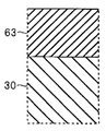
すなわち、図11Aに示すように、50at%非晶質炭素と50at%Snとからなる厚さ5nmの混合層63をカンチレバー本体(突起部30)の表面に堆積させた。
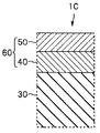
混合層63は加熱処理(250℃)により、図11Bに示す結晶性炭素複合層60に変化した。
混合層63のSnの含有率は、全体の1at%~99at%の範囲内とすることができる。
なお、混合層63のSnの含有率および加熱/冷却条件によっては、図11Cに示すように、内部に金属材料(Sn)を含む結晶性炭素層(グラフェン層50D)からなる結晶性炭素複合層60Dが形成される場合もある。表面に結晶性炭素複合層60Dが堆積されている変形例4のカンチレバー1Dでも、最表面はグラフェンで覆われているため、カンチレバー1等と同じ効果を有する。
なお、変形例2のカンチレバーの製造方法においても、条件によっては、晶性炭素複合層は、カンチレバー1Dと同じ構成、すなわち、金属内包構造となることがある。
<変形例5>
本変形例のカンチレバーの製造方法では、炭素原料層が堆積される工程と前記加熱工程とが同時に行われると見なされる。
本変形例のカンチレバーの製造方法では、炭素原料層が堆積される工程と前記加熱工程とが同時に行われると見なされる。
すなわち、図12に示すように、金属層堆積工程(S14)の後に、炭素原料供給工程(S16E)と加熱工程(S18E)とが同時に行われるグラフェン層堆積工程S17が行われる。
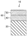
すなわち、図13Aに示すように、Snからなる厚さ1.5nmの金属層40をカンチレバー本体(突起部30)の表面に堆積させた。
ついで、炭素原料を供給しながら加熱処理を行うことで、冷却後には、図13Bに示すように、金属層40の上に、厚さ2nmのグラフェン層50が形成されたカンチレバー1Eが作製された。
具体的には、炭素原子を含む炭素原料ガスを供給しつつ加熱する。加熱は、真空中、不活性ガス雰囲気中、水素などの還元雰囲気中、大気中いずれでもよい。
なお、変形例2~5のカンチレバーにおいても、変形例1のカンチレバー1Aのように金属層が島状でもよいことは言うまでも無い。
<変形例6、7>
カンチレバー1、1A~1Eの製造方法において、炭素複合層を金属材料と結晶性炭素とを含む結晶性炭素複合層に変化するための加熱工程の後に、さらに金属層40を除去する工程を有していてもよい。金属層除去工程は、例えば加熱工程と同じ温度で加熱工程の2倍以上の処理時間の追加加熱工程、加熱工程よりも高温の追加加熱工程、または、エッチング工程である。
カンチレバー1、1A~1Eの製造方法において、炭素複合層を金属材料と結晶性炭素とを含む結晶性炭素複合層に変化するための加熱工程の後に、さらに金属層40を除去する工程を有していてもよい。金属層除去工程は、例えば加熱工程と同じ温度で加熱工程の2倍以上の処理時間の追加加熱工程、加熱工程よりも高温の追加加熱工程、または、エッチング工程である。
追加加熱工程により金属層を構成している金属材料は、加熱温度が融点MP以上の場合には蒸発し、加熱温度が融点以下の場合には昇華し、消失する。
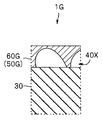
例えば、図14Aに示す変形例6のカンチレバー1Fでは、グラフェン層(結晶性炭素層)50の下の金属層40Fの一部が空洞40Xである。さらに図14Bに示す変形例7のカンチレバー1Gでは、金属層が消失し、グラフェン層(結晶性炭素層60G)50Gの一部が空洞40Xとなっている。
また、金属層除去工程により、カンチレバーは、見かけ上、グラフェン層が基体に直接、堆積されたようになる。金属層が除去されたカンチレバーは、先端部の曲率半径Rがより小さくなるため、より高い空間分解能を示す。
<変形例8、9>
以上の説明では、グラフェン層50が、突起部30が形成されている上面SAを覆っているカンチレバー1、1A~1Gについて説明した。しかし、分解能に影響を及ぼすのは、突起部30の先端部に堆積された導電層の厚さである。
以上の説明では、グラフェン層50が、突起部30が形成されている上面SAを覆っているカンチレバー1、1A~1Gについて説明した。しかし、分解能に影響を及ぼすのは、突起部30の先端部に堆積された導電層の厚さである。
図15Aに示す変形例8のカンチレバー1Hでは、突起部30の根元部、レバー部および支持部に、厚さの0.2μmのアルミニウムからなる導電金属層70が堆積されている。例えば、グラフェン層50を堆積後にカンチレバーの全面をアルミニウム層で覆い、その後、先端部のアルミニウム層を選択的に除去することでカンチレバー1Hは作製される。
突起部30の先端部には、厚さが薄くでも高い導電性を示すグラフェン層50だけが堆積されている。すなわち、グラフェン層50は電気抵抗が低いが、厚さが十分に厚い金、白金、またはアルミニウム等からなる導電金属層70は、グラフェン層50よりも更に電気抵抗が小さく堆積が容易である。このため、カンチレバー1Hは、カンチレバー1等と同じ空間分解能であり、かつ、より電気抵抗が低い。
なお、導電金属層70は、あまり厚いとカンチレバーのレバー部20の厚さを厚くし、機械的特性が劣化する。このため導電金属層70の厚さは、1μm以下が好ましく、0.3μm以下が特に好ましい。
なお、図15Bに示す変形例9のカンチレバー1Iのように、突起部30の先端部だけに、グラフェン層50と金属層40を含むグラフェン複合層60が堆積されていてもよいことは言うまでも無い。なお、カンチレバー1Iでは、グラフェン複合層60の堆積後に、導電金属層70が堆積されている。これに対して、導電金属層70を堆積後にグラフェン複合層60を堆積してもよい。
<変形例10>
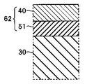
図16Aに示すように、変形例10のカンチレバー1Jでは、まず、非晶質炭素からなる厚さ1.5nmの炭素原料層51をカンチレバー本体(突起部30)の表面に、堆積させた。さらに、炭素原料層51の上に、In(インジウム)からなる厚さ3nmの金属層40を堆積させた。すなわち、炭素複合層62は、炭素原料層51と炭素原料層51の上の金属層40とからなる。
図16Aに示すように、変形例10のカンチレバー1Jでは、まず、非晶質炭素からなる厚さ1.5nmの炭素原料層51をカンチレバー本体(突起部30)の表面に、堆積させた。さらに、炭素原料層51の上に、In(インジウム)からなる厚さ3nmの金属層40を堆積させた。すなわち、炭素複合層62は、炭素原料層51と炭素原料層51の上の金属層40とからなる。
真空中で170℃、1時間の加熱を行い、その後、室温まで冷却した。すると、図16Bに示すように、炭素複合層62は、金属層40と、金属層40の上の第1のグラフェン層50Aと、金属層40の下の第2のグラフェン層50Bと、からなる結晶性炭素複合層60Jに変化した。
インジウムの融点(MP)は、157℃である。このため、170℃の加熱工程ではインジウムは溶融し、溶融インジウムに溶解した炭素が拡散し、第1のグラフェン層50Aとして金属層40の上に再析出する。
そして、変形例2のカンチレバー1Bに対する説明のように、炭素原料層51の一部は、再析出により金属層40の下の第2のグラフェン層50Bとなる。なお、第2のグラフェン層50Bは第1のグラフェン層50Aよりも薄い。
また、カンチレバー1Jは、加熱工程の温度が150℃、すなわち、インジウムの融点MP未満であっても、結晶性炭素複合層62は、金属層40と、金属層40の上の第1のグラフェン層50Aと、金属層40の下の第2のグラフェン層50Bとなった。
さらに、金属層40として、主成分の金属よりも低融点の合金材料を用いても良い。例えば、SnIn合金の融点は、Snの融点(230℃)およびInの融点(157℃)よりも低い、例えば117℃である。低融点の金属層40を有するカンチレバーは、さらに低温の加熱処理により作製できる。例えば、融点MPが117℃の金属層を有するカンチレバーは、100℃以下の97℃(MP-20℃)でも作製できる。
<変形例11>
図17のフローチャートに示すように、変形例11のカンチレバー1Kの製造方法は、金属層40を除去する工程(ステップS19)を更に具備する。
図17のフローチャートに示すように、変形例11のカンチレバー1Kの製造方法は、金属層40を除去する工程(ステップS19)を更に具備する。
カンチレバー1Kの製造方法では、まず、非晶質炭素からなる厚さ10nmの炭素原料層51をカンチレバー本体(突起部30)の表面に、堆積させた。さらに、炭素原料層51の上に、融点MPが120℃のIn-Sn合金からなる厚さ50nmの金属層40を堆積させた。すなわち、炭素複合層62は、炭素原料層51と炭素原料層51の上の金属層40とからなる。
そして、窒素中で100℃、1時間の加熱を行い、その後、室温まで冷却する加熱処理を行った。炭素複合層62は加熱処理により、図16Bに示した結晶性炭素複合層62と同じように、金属層40と、金属層40の上の第1のグラフェン層50Aと、金属層40の下の第2のグラフェン層50Bに変化する
さらに、カンチレバー1Kの製造方法では、加熱工程(ステップS18)の後に金属層40を除去する工程(ステップS19)が行われた。すなわち、酸性溶液(10重量%硝酸)によるケミカルエッチング工程により、金属層40および第1のグラフェン層50Aが除去された。第1のグラフェン層50Aは酸性溶液には溶解しない。しかし、ケミカルエッチング工程により金属層40が溶解すると、その上の第1のグラフェン層50Aもカンチレバーから剥離される。
図18に示すように、カンチレバー1Kの先端部には、第2のグラフェン層50Bだけが堆積されている。第2のグラフェン層50Bの厚さは、2nmであり、先端部の曲率半径Rは、6nmであった。すなわち、第2のグラフェン層50Bの厚さは、8nmであると推定される第1のグラフェン層50Aの厚さよりも薄い。そして、厚い第1のグラフェン層50Aおよび金属層40は除去され薄い第2のグラフェン層50Bだけがカンチレバー1Kの先端部に残っている。
なお、加熱処理として、真空中で130℃、0.5時間の加熱を行った場合にも、カンチレバー1Kと略同じ構成のカンチレバーが作製された。
また、変形例9のカンチレバー1Iのように、第2のグラフェン層50Bが突起部30の先端部だけに堆積されていてもよい。
本発明の製造方法によって製造されたカンチレバーは、その製造方法を特定することは現実的ではない。例えば、図18に示した変形例11のカンチレバー1Kが、金属層除去工程(S19)において第1の金属層50Aおよび第1のグラフェン層50Aが除去されていることを立証することは非常に困難である。例えば、本発明のカンチレバーの製造方法により製造されたカンチレバーは、基体とグラフェン層との界面の状態が、従来の製造方法により製造されたカンチレバーと異なっている可能性がある。しかし、界面の構造、例えば、結晶構造が、透過型電子顕微鏡等を用いて解析できたとしても、その構造から製造方法を立証することはできない。
また、加熱工程の温度が450℃以下であることも、製造後に特定することは出来ない。すなわち、本発明のカンチレバーの製造方法により製造されたカンチレバーは、従来技術との相違に係る構造又は特性を特定する文言を見いだすことができず、かつ、かかる構造又は特性を測定に基づき解析し特定することも不可能又は非実際的である。
本発明は、上述した実施形態等に限定されるものではなく、本発明の要旨を変えない範囲において、種々の変更、改変、例えば、実施形態の構成要素の組み合わせ等が可能である。
本出願は、2016年3月17日に日本国に出願された特許出願2016-054095号を優先権主張の基礎として出願するものであり、上記の開示内容は、本願明細書、請求の範囲、図面に引用されたものとする。
1、1A~1K・・・カンチレバー
2・・・治具
2A・・・導線
4・・・試料
10・・・支持部
20・・・レバー部
30・・・突起部
40・・・金属層
50・・・グラフェン層
51・・・炭素原料層
60・・・グラフェン複合層
61・・・炭素複合層
63・・・混合層
2・・・治具
2A・・・導線
4・・・試料
10・・・支持部
20・・・レバー部
30・・・突起部
40・・・金属層
50・・・グラフェン層
51・・・炭素原料層
60・・・グラフェン複合層
61・・・炭素複合層
63・・・混合層
Claims (20)
- 走査型プローブ顕微鏡に用いられる、支持部とレバー部と探針である突起部とを含むカンチレバーであって、
前記突起部の先端部に、結晶性炭素ナノ材料と融点が420℃以下の金属材料とを含む結晶性炭素複合層が、堆積されていることを特徴とするカンチレバー。 - 前記結晶性炭素複合層の厚さが、7nm以下であり、前記先端部の曲率半径が、10nm以下であることを特徴とする請求項1に記載のカンチレバー。
- 前記金属材料が、Zn、Sn、Bi、Pb、Tl、Cs、In、Cd、Rb、Ga、K、Na、Se、および、Liの少なくともいずれかを含むことを特徴とする請求項2に記載のカンチレバー。
- 前記金属材料の融点が、250℃以下であることを特徴とする請求項3に記載のカンチレバー。
- 前記金属材料が、Sn、Zn、Bi、In、およびSeの少なくともいずれかを含むことを特徴とする請求項4に記載のカンチレバー。
- 前記結晶性炭素複合層が、前記結晶性炭素ナノ材料からなる結晶性炭素層と、前記金属材料からなる金属層と、を含むことを特徴とする請求項1から請求項5のいずれか1項に記載のカンチレバー。
- 支持部とレバー部と探針である突起部とを含むカンチレバー本体の前記突起部の先端部に、結晶性炭素ナノ材料からなる結晶性炭素層が堆積されているカンチレバーの製造方法であって、
前記カンチレバー本体が作製される工程と、
前記突起部の前記先端部に、融点が420℃以下の金属材料と炭素原料とを含む炭素複合層が堆積される炭素複合層堆積工程と、
前記炭素複合層を、前記結晶性炭素層と前記金属材料からなる金属層とを含む結晶性炭素複合層とする温度が450℃以下の、加熱工程と、を具備することを特徴とするカンチレバーの製造方法。 - 前記炭素複合層の厚さが、7nm以下であり、前記先端部の曲率半径が、10nm以下であることを特徴とする請求項7に記載のカンチレバーの製造方法。
- 前記金属材料が、Zn、Sn、Bi、Pb、Tl、Cs、In、Cd、Rb、Ga、K、Na、Se、および、Liの少なくともいずれかを含むことを特徴とする請求項8に記載のカンチレバーの製造方法。
- 前記金属材料の融点が、250℃以下であることを特徴とする請求項9に記載のカンチレバーの製造方法。
- 前記金属材料が、Sn、Zn、Bi、In、およびSeの少なくともいずれかを含むことを特徴とする請求項10に記載のカンチレバーの製造方法。
- 前記加熱工程の前記温度が、前記金属材料の融点以上であることを特徴とする請求項9から請求項11のいずれか1項に記載のカンチレバーの製造方法。
- 前記加熱工程の前記温度が、(前記金属材料の融点-20℃)以上、前記金属材料の融点未満であることを特徴とする請求項9から請求項11のいずれか1項に記載のカンチレバーの製造方法。
- 前記炭素複合層堆積工程が、前記金属材料を含む金属層が堆積される工程と、前記金属層の上に前記炭素原料を含む炭素原料層が堆積される工程と、を含むことを特徴とする請求項9から請求項13のいずれか1項に記載のカンチレバーの製造方法。
- 前記炭素複合層堆積工程が、前記炭素原料を含む炭素原料層が堆積される工程と、前記炭素原料層の上に前記金属材料を含む金属層が堆積される工程と、を含むことを特徴とする請求項9から請求項13のいずれか1項に記載のカンチレバーの製造方法。
- 前記炭素複合層堆積工程が、前記炭素原料と前記金属材料とが混合した混合層が堆積される工程であることを特徴とする請求項9から請求項13のいずれか1項に記載のカンチレバーの製造方法。
- 前記加熱工程の後に、前記結晶性炭素複合層から、前記金属材料を除去する工程を、更に具備することを特徴とする請求項9から請求項16のいずれか1項に記載のカンチレバーの製造方法。
- 前記金属材料を除去する工程が、前記金属材料からなる金属層と、前記金属層の上の第1の結晶性炭素層と、前記金属層の下の第2の結晶性炭素層と、を含む前記結晶性炭素複合層から、前記金属層および前記第1の結晶性炭素層が除去され、前記第2の結晶性炭素層は除去されないケミカルエッチング工程であることを特徴とする請求項17に記載のカンチレバーの製造方法。
- 支持部とレバー部と探針である突起部とを含むカンチレバー本体の前記突起部の先端部に、グラフェン層が堆積されている、走査型プローブ顕微鏡に用いられるカンチレバーの製造方法であって、
前記カンチレバー本体が作製される工程と、
前記突起部の前記先端部に、炭素原料を含む炭素原料層が堆積され、さらに前記炭素原料層の上に、SnまたはInを主成分する金属材料からなる金属層が堆積される炭素複合層堆積工程と、
加熱温度が、(前記金属材料の融点-20℃)以上(前記金属材料の前記融点+30℃)以下の加熱工程と、
前記金属層を除去するケミカルエッチング工程と、を具備することを特徴とするカンチレバーの製造方法。 - 請求項9から請求項19のいずれか1項に記載のカンチレバーの製造方法により製造されたことを特徴とするカンチレバー。
Priority Applications (2)
| Application Number | Priority Date | Filing Date | Title |
|---|---|---|---|
| JP2018505312A JP6754123B2 (ja) | 2016-03-17 | 2017-01-26 | カンチレバーおよびカンチレバーの製造方法 |
| US16/121,729 US10545172B2 (en) | 2016-03-17 | 2018-09-05 | Cantilever and manufacturing method for cantilever |
Applications Claiming Priority (2)
| Application Number | Priority Date | Filing Date | Title |
|---|---|---|---|
| JP2016054095 | 2016-03-17 | ||
| JP2016-054095 | 2016-03-17 |
Related Child Applications (1)
| Application Number | Title | Priority Date | Filing Date |
|---|---|---|---|
| US16/121,729 Continuation US10545172B2 (en) | 2016-03-17 | 2018-09-05 | Cantilever and manufacturing method for cantilever |
Publications (1)
| Publication Number | Publication Date |
|---|---|
| WO2017159062A1 true WO2017159062A1 (ja) | 2017-09-21 |
Family
ID=59851640
Family Applications (1)
| Application Number | Title | Priority Date | Filing Date |
|---|---|---|---|
| PCT/JP2017/002804 Ceased WO2017159062A1 (ja) | 2016-03-17 | 2017-01-26 | カンチレバーおよびカンチレバーの製造方法 |
Country Status (3)
| Country | Link |
|---|---|
| US (1) | US10545172B2 (ja) |
| JP (1) | JP6754123B2 (ja) |
| WO (1) | WO2017159062A1 (ja) |
Cited By (3)
| Publication number | Priority date | Publication date | Assignee | Title |
|---|---|---|---|---|
| JP2020105040A (ja) * | 2018-12-26 | 2020-07-09 | シーズテクノ株式会社 | 基板上のグラフェン膜の直接成膜法及び走査型プローブ顕微鏡用カンチレバー |
| KR20220105320A (ko) * | 2021-01-20 | 2022-07-27 | 인천대학교 산학협력단 | 시료 표면의 전기장 분포 분석 장치 |
| WO2025194107A1 (en) * | 2024-03-14 | 2025-09-18 | Bruke Nano, Inc. | High frequency passivated afm cantilever and method of fabrication |
Citations (2)
| Publication number | Priority date | Publication date | Assignee | Title |
|---|---|---|---|---|
| WO2014011954A1 (en) * | 2012-07-13 | 2014-01-16 | Northwestern University | Multifunctional graphene coated scanning tips |
| CN104360107A (zh) * | 2014-11-12 | 2015-02-18 | 苏州大学 | 一种石墨烯包覆原子力显微镜探针及其制备方法、用途 |
Family Cites Families (13)
| Publication number | Priority date | Publication date | Assignee | Title |
|---|---|---|---|---|
| US6339217B1 (en) * | 1995-07-28 | 2002-01-15 | General Nanotechnology Llc | Scanning probe microscope assembly and method for making spectrophotometric, near-field, and scanning probe measurements |
| US6755956B2 (en) * | 2000-10-24 | 2004-06-29 | Ut-Battelle, Llc | Catalyst-induced growth of carbon nanotubes on tips of cantilevers and nanowires |
| US7151256B2 (en) * | 2003-11-19 | 2006-12-19 | Ut-Battelle, Llc | Vertically aligned nanostructure scanning probe microscope tips |
| JP4761129B2 (ja) * | 2005-11-30 | 2011-08-31 | 株式会社ユニソク | プローブ顕微鏡用探針の作製方法、及びプローブ顕微鏡 |
| JP4798454B2 (ja) * | 2007-02-19 | 2011-10-19 | オリンパス株式会社 | 細胞内及び細胞間の微小空間計測用カンチレバーシステム |
| JP5216509B2 (ja) * | 2008-03-05 | 2013-06-19 | 株式会社日立製作所 | 走査プローブ顕微鏡およびこれを用いた試料の観察方法 |
| CN102438944B (zh) | 2009-03-27 | 2014-07-16 | 独立行政法人科学技术振兴机构 | 石墨烯膜的制造方法、电子元件的制造方法及石墨烯膜向基板的转印方法 |
| CN103140439B (zh) | 2010-07-15 | 2017-06-09 | 石墨烯广场株式会社 | 低温生产石墨烯的方法,直接转移用相同方法的石墨烯的方法与石墨烯片材 |
| US8835286B2 (en) * | 2010-11-04 | 2014-09-16 | Nec Corporation | Manufacturing method of graphene substrate and graphene substrate |
| CN102353817B (zh) | 2011-06-30 | 2013-07-31 | 中国科学院苏州纳米技术与纳米仿生研究所 | 导电原子力显微镜的探针以及采用此探针的测量方法 |
| JP2013098396A (ja) | 2011-11-02 | 2013-05-20 | Nagoya Institute Of Technology | グラフェン構造の製造方法及びこれを用いた半導体装置の製造方法 |
| WO2014090938A1 (en) | 2012-12-14 | 2014-06-19 | Universitat Autonoma De Barcelona | Conductive atomic force microscope tips coated with graphene |
| US9616470B1 (en) * | 2016-09-13 | 2017-04-11 | International Business Machines Corporation | Cleaning of nanostructures |
-
2017
- 2017-01-26 JP JP2018505312A patent/JP6754123B2/ja not_active Expired - Fee Related
- 2017-01-26 WO PCT/JP2017/002804 patent/WO2017159062A1/ja not_active Ceased
-
2018
- 2018-09-05 US US16/121,729 patent/US10545172B2/en active Active
Patent Citations (2)
| Publication number | Priority date | Publication date | Assignee | Title |
|---|---|---|---|---|
| WO2014011954A1 (en) * | 2012-07-13 | 2014-01-16 | Northwestern University | Multifunctional graphene coated scanning tips |
| CN104360107A (zh) * | 2014-11-12 | 2015-02-18 | 苏州大学 | 一种石墨烯包覆原子力显微镜探针及其制备方法、用途 |
Cited By (4)
| Publication number | Priority date | Publication date | Assignee | Title |
|---|---|---|---|---|
| JP2020105040A (ja) * | 2018-12-26 | 2020-07-09 | シーズテクノ株式会社 | 基板上のグラフェン膜の直接成膜法及び走査型プローブ顕微鏡用カンチレバー |
| KR20220105320A (ko) * | 2021-01-20 | 2022-07-27 | 인천대학교 산학협력단 | 시료 표면의 전기장 분포 분석 장치 |
| KR102503113B1 (ko) * | 2021-01-20 | 2023-02-23 | 인천대학교 산학협력단 | 시료 표면의 전기장 분포 분석 장치 |
| WO2025194107A1 (en) * | 2024-03-14 | 2025-09-18 | Bruke Nano, Inc. | High frequency passivated afm cantilever and method of fabrication |
Also Published As
| Publication number | Publication date |
|---|---|
| US20190018042A1 (en) | 2019-01-17 |
| US10545172B2 (en) | 2020-01-28 |
| JPWO2017159062A1 (ja) | 2019-01-17 |
| JP6754123B2 (ja) | 2020-09-09 |
Similar Documents
| Publication | Publication Date | Title |
|---|---|---|
| Lahiri et al. | Carbon nanotubes: how strong is their bond with the substrate? | |
| Pan et al. | Molten gallium as a catalyst for the large-scale growth of highly aligned silica nanowires | |
| US6764874B1 (en) | Method for chemical vapor deposition of single walled carbon nanotubes | |
| JP4521482B2 (ja) | Spmカンチレバー及びその製造方法 | |
| CN101811658B (zh) | 碳纳米管阵列传感器及其制备方法 | |
| EP1096533A1 (en) | Method for fabrication of patterned carbon nanotube films | |
| US20120034707A1 (en) | Atomically precise nanoribbons and related methods | |
| US20080098805A1 (en) | Nanotube-Based Nanoprobe Structure and Method for Making the Same | |
| EP3003973B1 (fr) | Substrat conducteur electrique sur au moins une de ses faces muni d'un empilement de couches minces pour la croissance de nanotubes de carbone (ntc) | |
| JP6754123B2 (ja) | カンチレバーおよびカンチレバーの製造方法 | |
| JP4231228B2 (ja) | マイクロマシーン | |
| Vogl et al. | Transforming layered MoS 2 into functional MoO 2 nanowires | |
| JP5027100B2 (ja) | 先端上で整列したナノ構造 | |
| CN102175894A (zh) | 一种扫描热显微镜微型热电偶探针的制备方法 | |
| US7814565B2 (en) | Nanostructure on a probe tip | |
| US20090320991A1 (en) | Methods of synthesis of nanotubes and uses thereof | |
| Pacios et al. | Direct manufacturing of ultrathin graphite on three-dimensional nanoscale features | |
| JP4684053B2 (ja) | カーボンナノチューブの作製方法及びその固定方法 | |
| US7707962B2 (en) | Apparatus for forming carbon nanotube film | |
| US8604459B1 (en) | Electrical devices containing a carbon nanotube switching layer with a passivation layer disposed thereon and methods for production thereof | |
| JP2007518067A5 (ja) | ナノ構造体チップの製造方法及びその装置 | |
| Zang et al. | Graphene synthesis via droplet CVD AND its photonic applications | |
| TWI408246B (zh) | 分枝型奈米碳管之製備方法 | |
| Ižák et al. | Analysis of catalytic growth of carbon nanotubes by ACCVD method | |
| JP2010210449A (ja) | 導電性ナノチューブ探針、それを用いた電気特性評価装置及び走査型プローブ顕微鏡 |
Legal Events
| Date | Code | Title | Description |
|---|---|---|---|
| ENP | Entry into the national phase |
Ref document number: 2018505312 Country of ref document: JP Kind code of ref document: A |
|
| NENP | Non-entry into the national phase |
Ref country code: DE |
|
| 121 | Ep: the epo has been informed by wipo that ep was designated in this application |
Ref document number: 17766070 Country of ref document: EP Kind code of ref document: A1 |
|
| 122 | Ep: pct application non-entry in european phase |
Ref document number: 17766070 Country of ref document: EP Kind code of ref document: A1 |