WO2017154337A1 - オゾン生成用素子およびオゾン生成装置 - Google Patents
オゾン生成用素子およびオゾン生成装置 Download PDFInfo
- Publication number
- WO2017154337A1 WO2017154337A1 PCT/JP2017/000752 JP2017000752W WO2017154337A1 WO 2017154337 A1 WO2017154337 A1 WO 2017154337A1 JP 2017000752 W JP2017000752 W JP 2017000752W WO 2017154337 A1 WO2017154337 A1 WO 2017154337A1
- Authority
- WO
- WIPO (PCT)
- Prior art keywords
- electrode
- ozone
- distance
- ozone generation
- dielectric substrate
- Prior art date
- Legal status (The legal status is an assumption and is not a legal conclusion. Google has not performed a legal analysis and makes no representation as to the accuracy of the status listed.)
- Ceased
Links
Images







Classifications
-
- C—CHEMISTRY; METALLURGY
- C01—INORGANIC CHEMISTRY
- C01B—NON-METALLIC ELEMENTS; COMPOUNDS THEREOF; METALLOIDS OR COMPOUNDS THEREOF NOT COVERED BY SUBCLASS C01C
- C01B13/00—Oxygen; Ozone; Oxides or hydroxides in general
- C01B13/10—Preparation of ozone
- C01B13/11—Preparation of ozone by electric discharge
- C01B13/115—Preparation of ozone by electric discharge characterised by the electrical circuits producing the electrical discharge
-
- C—CHEMISTRY; METALLURGY
- C01—INORGANIC CHEMISTRY
- C01B—NON-METALLIC ELEMENTS; COMPOUNDS THEREOF; METALLOIDS OR COMPOUNDS THEREOF NOT COVERED BY SUBCLASS C01C
- C01B13/00—Oxygen; Ozone; Oxides or hydroxides in general
- C01B13/10—Preparation of ozone
- C01B13/11—Preparation of ozone by electric discharge
-
- C—CHEMISTRY; METALLURGY
- C01—INORGANIC CHEMISTRY
- C01B—NON-METALLIC ELEMENTS; COMPOUNDS THEREOF; METALLOIDS OR COMPOUNDS THEREOF NOT COVERED BY SUBCLASS C01C
- C01B2201/00—Preparation of ozone by electrical discharge
- C01B2201/20—Electrodes used for obtaining electrical discharge
- C01B2201/22—Constructional details of the electrodes
-
- C—CHEMISTRY; METALLURGY
- C01—INORGANIC CHEMISTRY
- C01B—NON-METALLIC ELEMENTS; COMPOUNDS THEREOF; METALLOIDS OR COMPOUNDS THEREOF NOT COVERED BY SUBCLASS C01C
- C01B2201/00—Preparation of ozone by electrical discharge
- C01B2201/30—Dielectrics used in the electrical dischargers
- C01B2201/32—Constructional details of the dielectrics
Definitions
- the present invention relates to an ozone generating element and an ozone generating apparatus.
- An element for generating ozone which includes a dielectric substrate, a pair of electrodes provided on the dielectric substrate, and a dielectric layer covering the pair of electrodes, and generates ozone by generating creeping discharge between the pair of electrodes.
- each electrode of the ozone generating element has a comb-like shape having a linear wiring and a plurality of linear members extending in one direction orthogonal to the extending direction of the wiring, The electrode linear member and the other electrode linear member are alternately arranged at regular intervals.
- the ozone generating element described in Patent Document 1 suppresses heat generation during operation by increasing the thickness of the dielectric substrate to increase the heat capacity of the dielectric substrate or using it with a cooler. In addition, a decrease in the amount of ozone generated is suppressed.
- the present invention has been made in view of the above reasons, and an object of the present invention is to provide an ozone generating element and an ozone generating device that are small and have high ozone generation efficiency.
- an element for generating ozone comprises: A dielectric substrate; A first comb electrode and a second comb electrode provided on one main surface of the dielectric substrate;
- the first comb electrode has a first terminal electrode part and a plurality of first electrode parts intersecting the first terminal electrode part
- the second comb-shaped electrode has a second terminal electrode part and a plurality of second electrode parts intersecting the second terminal electrode part,
- the first electrode part and the second electrode part are arranged to be alternately arranged in one direction,
- a first distance which is an interval between the first electrode element part and the second electrode element part adjacent to the first electrode element part in one direction, is the first electrode element part and the first electrode element part.
- the ratio of the second distance to the first distance is 1.1 or more and 4.0 or less.
- the ozone generating element according to the present invention is The ratio of the second distance to the first distance may be 1.5 or more and 2.5 or less.
- the ozone generating element according to the present invention is It may further include a dielectric layer covering the one main surface of the dielectric substrate.
- the ozone generating element according to the present invention is The first electrode part and the second electrode part may be connected to the first terminal electrode part and the second terminal electrode part, respectively.
- the ozone generator according to the present invention is The ozone generating element; An AC power supply for applying an AC voltage between the first comb electrode and the second comb electrode.
- the first distance which is the distance between the first electrode part and the second electrode part adjacent to the first electrode part on one side
- the second distance which is the distance between the first electrode part and the second electrode part adjacent in the other direction.
- the ozone generating element according to the present invention has a higher ozone generation efficiency than the ozone generating element in which the first distance and the second distance are equal, and reduces ozone depletion due to ozone decomposition due to heat generated during operation. Since ozone that only cancels out can be generated, an ozone generation amount equal to or greater than that of the element for generating ozone having the same first distance and second distance can be secured. Therefore, it is not necessary to increase the thickness of the dielectric substrate or to use the dielectric substrate together with a cooler, so that the ozone generating element or the entire module including the ozone generating element can be reduced in size.
- FIG. 5 is a cross-sectional view of the ozone generating element according to the comparative example taken along the line CC of FIG. 4.
- FIG. 5 is a cross-sectional view of the ozone generating element according to the comparative example taken along the line CC of FIG. 4.
- FIG. 3 is a cross-sectional view of the ozone generation element according to the embodiment, taken along line AA in FIG. 2. It is sectional drawing for demonstrating the manufacturing method of the element for ozone generation which concerns on embodiment. It is sectional drawing for demonstrating the manufacturing method of the element for ozone generation which concerns on embodiment. It is sectional drawing for demonstrating the manufacturing method of the element for ozone generation which concerns on embodiment. It is sectional drawing for demonstrating the manufacturing method of the element for ozone generation which concerns on embodiment. It is sectional drawing for demonstrating the manufacturing method of the element for ozone generation which concerns on embodiment. It is sectional drawing for demonstrating the manufacturing method of the element for ozone generation which concerns on embodiment. It is sectional drawing for demonstrating the manufacturing method of the element for ozone generation which concerns on embodiment. It is sectional drawing for demonstrating the manufacturing method of the element for ozone generation which concerns on embodiment.
- FIG. 9 is a plan view in which a dielectric layer of an ozone generation element according to Modification 1 is
- the ozone generation apparatus includes an ozone generation element 10 and an AC power supply 31 that applies an AC voltage to the ozone generation element 10.
- the ozone generating element 10 has a plate shape having a longitudinal direction and a transverse direction, and includes a dielectric substrate 13, a pair of electrodes 21A and 21B, a dielectric layer 12, back electrodes 25A and 25B, and a plug. 26A, 26B.
- the thickness direction of the ozone generating element 10 in FIG. 1 is appropriately set to the Z direction, and the direction from the dielectric substrate 13 to the dielectric layer 12 in the Z direction is the + Z direction or upward.
- the longitudinal direction of the ozone generation element 10 orthogonal to the X axis direction, the Z axis direction, and the short direction of the ozone generation element 10 orthogonal to the X axis direction will be described as the Y axis direction.
- the dielectric substrate 13 has a rectangular plate shape. Contact holes 131A and 131B penetrating the dielectric substrate 13 in the thickness direction are formed at both ends of the dielectric substrate 13 in the Y-axis direction in FIG. Plugs 26A and 26B are disposed in the contact holes 131A and 131B, respectively.
- the dielectric substrate 13 is made of a ceramic material containing an oxide such as CaO—B 2 O 3 —Al 2 O 3 —SiO 2 , Al 2 O 3 , SiO 2 , ZrO 2 , BaTiO 3 . Further, the dielectric substrate 13 may be formed of a LTCC (Low Temperature Co-fired Ceramics) substrate.
- the dielectric substrate 13 is not limited to a ceramic material as long as it has electrical insulation, and may be formed from a resin material such as an epoxy resin or a polyimide resin.
- the electrodes 21 ⁇ / b> A and 21 ⁇ / b> B are provided on the upper surface of the dielectric substrate 13.
- the pair of electrodes 21A and 21B includes a plurality (seven in FIG. 2) of electrode element portions 22A and 22B, terminal electrode portions 23A and 23B, and tongue pieces 24A and 24B.
- Electrodes 21A, 21B is, Cu, Ag, Pd, Pt , and is formed of a conductive oxide such as a metal or RuO 2 of W or the like.
- the electrodes 21A and 21B are made of metal, they can diffuse to the dielectric substrate 13 and the dielectric layer 12 during the baking process of the electrodes 21A and 21B. .
- the dielectric material which is the basis of the dielectric substrate 13 and the dielectric layer 12 is not sufficiently sintered, and the voltage resistance of the dielectric substrate 13 and the dielectric layer 12 may be reduced.
- the electrodes 21A, 21B are preferably formed of a conductive oxide such as RuO 2.
- the thickness of the electrodes 21A and 21B is set to about 10 ⁇ m.
- the electrodes 21A and 21B correspond to the first comb electrode and the second comb electrode of the present invention.
- the terminal electrode portion 23A corresponds to the first terminal electrode portion of the present invention, and the terminal electrode portion 23b corresponds to the second terminal electrode portion of the present invention.
- the electrode portion 22A corresponds to the first electrode portion of the present invention, and the electrode portion 22b corresponds to the second electrode portion of the present invention.
- the plurality of electrode portions 22A and 22B are arranged side by side in the X-axis direction.
- Each electrode part 22A, 22B has an elongated shape having a longitudinal direction and a short direction, and extends in the Y-axis direction so as to intersect with the terminal electrode parts 23A, 23B.
- the terminal electrode portion 23A (23B) has an elongated shape and extends in the X-axis direction.
- the plurality of electrode parts 22A (22B) have a comb shape together with the terminal electrode part 23A (23B).
- electrode part 22B of electrode 21B is arrange
- the electrode element 22A of the electrode 21A is disposed between two electrode element parts 22B adjacent to each other in the X-axis direction of the electrode 21B. That is, the pair of electrodes 21A and 21B has a so-called interdigital structure in which electrode portions 22A and electrode portions 22B are alternately arranged in the X-axis direction.
- the distance (first distance) W11 between each electrode element 22B and the electrode element 22A arranged adjacent to each other on the + X direction side that is one side in the short direction is the electrode element 22B and its short distance. This is different from the distance (second distance) W12 between the electrode parts 22A arranged adjacent to each other on the ⁇ X direction side, which is the other side in the hand direction. Specifically, the distance W11 is shorter than the distance W12.
- the distance W11 corresponds to the distance between the electrode element part 22A on the + X direction side of the two adjacent electrode element parts 22A and the electrode element part 22B disposed between the two electrode element parts 22A. To do.
- the distance W12 is the distance between the electrode element 22A on the ⁇ X direction side of two adjacent electrode elements and the electrode element 22B disposed between the two electrode elements 22A. It corresponds to.
- the line width of the electrode portions 22A and 22B is W13.
- the tongue piece portion 24A extends in the ⁇ Y direction from the central portion of the terminal electrode portion 23A in the X-axis direction.
- the tongue piece 24A is electrically connected to a plug 26A disposed in the contact hole 131A.
- the tongue piece 24B extends in the + Y direction from the central portion of the terminal electrode portion 23B in the X-axis direction.
- the tongue piece 24B is electrically connected to a plug 26B disposed in the contact hole 131B.
- the dielectric layer 12 covers the electrodes 21 ⁇ / b> A and 21 ⁇ / b> B provided on the upper surface of the dielectric substrate 13.
- the dielectric layer 12 is made of a ceramic material containing an oxide such as CaO—B 2 O 3 —Al 2 O 3 —SiO 2 , Al 2 O 3 , SiO 2 , ZrO 2 , BaTiO 3 .
- the dielectric layer 12 may be made of an LTCC material.
- the dielectric substrate 13 is not limited to a ceramic material as long as it has electrical insulation, and may be formed from a resin material such as an epoxy resin or a polyimide resin.
- the dielectric layer 12 becomes high temperature by being exposed to plasma.
- the dielectric layer 12 is exposed to ozone generated in the vicinity of the surface thereof, erosion resistance against ozone is also required.
- the dielectric layer 12 is preferably formed of a ceramic material.
- the dielectric layer 12 is preferably made of a material whose thermal expansion coefficient is substantially equal to the thermal expansion coefficient of the dielectric substrate 13. In this case, even when the dielectric substrate 13 and the dielectric layer 12 expand and contract due to the heat generated during the operation of the ozone generating element 10, the junction between the dielectric substrate 13 and the dielectric layer 12 is distorted. Is unlikely to occur.
- the dielectric layer 12 is more preferably formed from the same material as the dielectric substrate 13.
- the back electrodes 25A and 25B are provided so as to cover at least the contact holes 131A and 131B of the dielectric substrate 13 on the surface of the dielectric substrate 13 opposite to the dielectric layer 12 side. Yes.
- the plug 26A is disposed in the contact hole 131A of the dielectric substrate 13 and electrically connects the electrode 21A and the back electrode 25A.
- the plug 26B is arranged in the contact hole 131B of the dielectric substrate 13, and electrically connects the electrode 21B and the back electrode 25B.
- the back electrodes 25A and 25B and the plugs 26A and 26B are made of a metal such as Cu, Ag, Pd, Pt, or W, or a conductive material such as RuO 2 .
- the AC power supply 31 is electrically connected to the back electrodes 25A and 25B, and applies an AC voltage (sine wave voltage) between the pair of electrodes 21A and 21B.
- the AC power supply 31 has a frequency sweep function or a resonance frequency tracking function, and the frequency of the AC voltage output to the ozone generation element 10 is the resonance frequency of a circuit configured by the AC power supply 31 and the ozone generation element 10. Adjust the frequency so that it is close. This reduces power loss in the circuit.
- the AC power supply 31 may apply a rectangular pulse train AC voltage between the electrodes 21A and 21B.
- the ozone generation element 10 As the ozone generation element 10 according to the present embodiment, seven types were prepared in which the distance W12 shown in FIG. 2 was set to 55 ⁇ m, 65 ⁇ m, 75 ⁇ m, 100 ⁇ m, 125 ⁇ m, 150 ⁇ m, and 200 ⁇ m.
- the seven types of ozone generating elements 10 all have electrode portions 22A and 22B with a width in the X-axis direction of 50 ⁇ m and a distance W11 in FIG. 2 of 50 ⁇ m.
- the dielectric substrate 13 has a square shape of 10 mm ⁇ 10 mm in plan view, and the thickness of the dielectric layer 12 is 15 ⁇ m.
- the total thickness of the dielectric substrate 13 and the dielectric layer 12 was about 600 ⁇ m.
- the length L1 in the X-axis direction and the length L2 in the Y-axis direction of the area where the portions excluding the tongue pieces 24A and 24B in the electrodes 21A and 21B on the dielectric substrate 13 are set to 8 mm.
- the electrode portions 922A of the electrodes 921A and the electrode portions 922B of the electrodes 921B are alternately arranged at a constant interval W91.
- the ozone generation element 910 an element having a distance W91 shown in FIG. 4 set to 50 ⁇ m was prepared.
- variety of the X-axis direction of all the electrode element parts 922A and 922B is 50 micrometers.
- the shape of the dielectric substrate 13, the thickness of the dielectric layer 12, the combined thickness of the dielectric substrate 13 and the dielectric layer 12, and the plurality of electrode portions of the electrodes 921A and 921B of the dielectric substrate 13 The dimensions of the region in which 922A and 922B and the terminal electrode portions 23A and 23B are provided are the same as those of the ozone generating element 10.
- the contents of the measurement of the discharge start voltage and the measurement of the ozone generation amount performed by the inventors to evaluate the discharge start voltage and the ozone generation amount of the ozone generation elements 10 and 910 will be described.
- the voltage amplitude value of the AC voltage (sine wave voltage) applied between the pair of electrodes 21A and 21B of the ozone generation element 10 or between the pair of electrodes 921A and 921B of the ozone generation element 910 is calculated.
- the presence or absence of plasma emission generated by the discharge was observed while gradually increasing.
- the voltage amplitude value at the time when plasma emission was observed was taken as the discharge start voltage.
- the ozone generation elements 10 and 910 are placed in an acrylic case having a volume of 7 liters, and the ozone concentration in the acrylic case when the ozone generation elements 10 and 910 are driven for 3 minutes is determined by ozone. Measured with a densitometer. Here, an alternating voltage (sine wave voltage) having a voltage amplitude value of 2.3 kV was applied between the pair of electrodes 21A and 21B of the ozone generation element 10 or between the pair of electrodes 921A and 921B of the ozone generation element 910. Moreover, a fan was provided in the acrylic case so that the gas in the acrylic case was stirred.
- ozone concentration meter model EG-3000 manufactured by Sugawara Jitsugyo Co., Ltd. was used.
- the amount of generated ozone five ozone generating elements 10 according to the embodiment and five ozone generating elements 910 according to the comparative examples are prepared, and the ozone concentration is adjusted for each of them as described above. It was measured.
- the average value of the discharge start voltage was 2.3 kV for any of the seven types of ozone generation elements 10 according to the embodiment and the ozone generation element 910 according to the comparative example. That is, there was no difference in the discharge start voltage between the ozone generation element 10 according to the embodiment and the ozone generation element 910 according to the comparative example.
- FIG. 5 shows the measurement result of the ozone generation amount for the ozone generation elements 10 and 910.
- the horizontal axis represents the distance W12 between the electrode element portions 22A and 22B shown in FIG. 2, and the vertical axis represents the ozone concentration.
- Black square marks indicate results for the ozone generation element 910 according to the comparative example, and white square marks indicate results for the ozone generation element 10 according to the embodiment.
- the ozone concentration was 39.50 ppm.
- the ozone concentration is 41.36 ppm, 40.65 ppm, 51.75 ppm, 55.19 ppm, and the distance W12 is 55 ⁇ m, 65 ⁇ m, 75 ⁇ m, 100 ⁇ m, 125 ⁇ m, 150 ⁇ m, and 200 ⁇ m, respectively. It was 51.28 ppm, 49.53 ppm, 51.03 ppm. From this result, the ozone concentration of the ozone generation element 10 according to the embodiment is all higher than the ozone concentration of the ozone generation element 910 according to the comparative example.
- the amount of generated ozone was increased when the distances W11 and W12 between the portions 22B were different from each other.
- the concentration of ozone generated by the ozone generating element 10 having a distance W12 of 75 ⁇ m or more is about 20% or more higher than the concentration of ozone generated by the ozone generating element 910 according to the comparative example. Obtained.
- the ratio of the distance W12 to the distance W11 of the ozone generation element 10 is at least 1.1 and not more than 4.0, the generation of ozone compared to the ozone generation element 910 according to the comparative example. It was found that the amount increased reliably. If the ratio of the distance W12 to the distance W11 of the ozone generation element 10 is 1.5 or more and 2.5 or less, the generation amount of ozone is about 20% or more compared to the ozone generation element 910 according to the comparative example. It turned out to increase. Therefore, the ratio of the distance W12 to the distance W11 of the ozone generating element 10 is preferably 1.5 or more and 2.5 or less.
- the reason why the ozone generation amount according to the embodiment shown in FIG. 5 is different from the ozone generation element 910 according to the comparative example will be described.
- the region A91 between the electrode portion 922A and the electrode portion 922B adjacent in the ⁇ X direction, which is the other side in the short side direction Electric fields E91 and E92 are generated in the region A92 between the electrode elements 922B adjacent in the + X direction, which is one side in the short direction.
- FIG. 6A shows a case where the potential of the electrode portion 922A is higher than the potential of the electrode portion 922B.
- V91 represents the acceleration of electrons accelerated by the electric field E91 in the region A91 and the X-axis component of the acceleration vector indicating the acceleration direction
- V92 represents the acceleration of electrons accelerated by the electric field E92 in the region A92.
- the X-axis component of the acceleration vector indicating the acceleration direction.
- the direction of the X-axis component V91 of the electron acceleration vector in the region A91 and the direction of the X-axis component V92 of the electron acceleration vector in the region A92 are opposite to each other. Further, the distances between the adjacent electrode element portions 922A and 922B are all equal. For this reason, the magnitudes of the electron acceleration directions V91 and V92 in the regions A91 and A92 are substantially the same. Then, for example, electrons accelerated in the + X direction in the region A91 are greatly decelerated in the ⁇ X direction when entering the region A92. In particular, at the boundary portion between the regions A91 and A92, the component in the X-axis direction of the electric field is substantially zero and the electrons are not accelerated. Therefore, the ozone generation element 910 according to the comparative example cannot give large energy to electrons, and the generation efficiency of ozone is low accordingly.
- the electrode part 22A and the electrode part 22B adjacent in the ⁇ X direction which is the other side in the short side direction
- the electric field E1 in the region A1 between the two is stronger than the electric field E2 in the region A2 between the electrode element 22A and the electrode element 22B adjacent in the + X direction, which is one side in the short direction.
- V1 indicates the acceleration of electrons accelerated by the electric field E1 in the region A1 and the X-axis component of the acceleration vector indicating the acceleration direction
- V2 indicates the acceleration of electrons accelerated by the electric field E2 in the region A2.
- the X-axis component of the acceleration vector indicating the acceleration direction.
- the magnitude of the X-axis component V1 of the electron acceleration vector in the region A1 is larger than the magnitude of the X-axis component V2 of the electron acceleration vector in the region A2.
- the electrons accelerated in the + X direction in the region A1 are hardly decelerated in the region A2, and are further accelerated in the + X direction in another region A1 adjacent in the + X direction of the region A2.
- the electrons have a large energy.
- generation efficiency of ozone is high to that extent.
- the ozone generation elements 10 and 910 a part of the ozone generated by the heat generated during the operation is decomposed, and the effective ozone generation amount is reduced.
- the ozone generation element 910 it is necessary to suppress a decrease due to ozone decomposition by cooling the ozone generating element 910.
- the ozone generation element 10 has higher ozone generation efficiency than the ozone generation element 910 as described above, and only cancels the decrease in ozone due to the decomposition of ozone due to the heat generated during operation. May generate ozone.
- the distance W12 between the electrode elements 22A and 22B of the ozone generating element 10 is extremely long (for example, when the ratio of the distance W12 to the distance W11 exceeds 4.0), the density of the electrode elements 22A and 22B is also increased. It decreases with it. Then, the amount of ozone generated due to the decrease in density of the electrode portions 22A and 22B that are ozone generation sources is reduced. Therefore, it is considered that the optimum range (1.5 or more and 2.5 or less) as described above exists in the ratio of the distance W12 to the distance W11 for the element 10 for ozone generation.
- the number of electrode portions 22A and 22B of the ozone generation element 10 according to the embodiment is smaller than the number of electrode portions 922A and 922B of the ozone generation element 910 according to the comparative example.
- the electrostatic capacity between the electrodes 21A and 21B of the ozone generating element 10 is smaller than the electrostatic capacity between the electrodes 921A and 921B of the ozone generating element 910.
- the load on the AC power supply 31 is reduced, so that the AC power supply 31 can be reduced in size.
- FIGS. 7A to 7D, 8A, and 8B are cross-sectional views at each step corresponding to the cross-sectional view of the ozone generating element 10 taken along the line BB in FIG.
- this manufacturing method first, a dielectric sheet serving as a base for the dielectric substrate 13 and the dielectric layer 12 is formed, and then a metal paste pattern serving as a base for the electrodes 21A, 21B and the like is formed on the dielectric sheet. Then, after laminating dielectric sheets, the laminated body of dielectric sheets is fired to produce the ozone generating element 10.
- a dielectric sheet (so-called ceramic green sheet) that forms the basis of the dielectric substrate 13 and the dielectric layer 12 is formed.
- a CaO—B 2 O 3 —Al 2 O 3 —SiO 2 glass, a mixed solvent of Al 2 O 3 , toluene and ethanol, a dispersant, a binder, and a ball mill are used.
- a slurry is prepared by pulverizing and mixing.
- a dielectric sheet is produced from the obtained slurry by a doctor blade method.
- the material used in the sheet forming step is not limited to the one containing the above-mentioned materials, but other types of glass other than CaO—B 2 O 3 —Al 2 O 3 —SiO 2 glass or SiO 2 , ZrO 2 , BaTiO 3 and other oxides may be included.
- a resin material such as an epoxy resin or a polyimide resin
- a resin material such as an epoxy resin or a polyimide resin may be used in the sheet forming step.
- a metal paste filling portion serving as a base of the plugs 26A and 26B is formed on a plurality of dielectric sheets used for the dielectric substrate 13.
- a through-hole 132A penetrating in the thickness direction is formed in the dielectric sheet 131 using a punching device such as a mechanical puncher.
- the through holes 132A are formed so as to be relatively at the same position when the dielectric sheets 131 are laminated.
- Ag paste is filled in each through hole 132 ⁇ / b> A of the dielectric sheet 131.
- the metal paste filling portion 261A is formed in the dielectric sheet 131.
- first metal paste patterns 211A and 211B that form the basis of the electrodes 21A and 21B are formed on the dielectric sheet disposed on the uppermost layer of the dielectric substrate 13 as shown in FIG. 7C. To do. Further, by using a screen printing technique, among the plurality of dielectric sheets used for the dielectric substrate 13 as shown in FIG. 7D, the back surface electrode 25A is applied to the dielectric sheet disposed in the lowermost layer of the dielectric substrate 13. A second metal paste pattern 251A serving as a base of 25B is formed.
- the first metal paste patterns 211A and 211B and the second metal paste pattern 251A are made of RuO 2 paste.
- a plurality of dielectric sheets 131 used for the dielectric substrate 13 are stacked, and the dielectric layer 12 is formed on the dielectric sheet 131 disposed on the top of the dielectric substrate 13.
- a single dielectric sheet 121 serving as a base is laminated.
- the dielectric sheets 121 and 131 are crimped by a crimping machine to obtain a laminate.
- the obtained laminate is fired at a firing temperature of 900 ° C.
- the dielectric sheets 121 and 131 are sintered to form the dielectric layers 12 and 132.
- the metal paste filling portion 261A, the first metal paste patterns 211A and 211B, and the second metal paste pattern 251A are sintered to form the conductive portion 262A, the electrodes 21A and 21B, and the back electrode 25A.
- the manufacturing method of the ozone generating element 10 requires only one firing process that is relatively laborious compared to other processes. Therefore, there is an advantage that the burden on the worker who is engaged in manufacturing the ozone generating element 10 is reduced.
- the ozone generation element 10 according to the present embodiment has a distance W11 different from the distance W12.
- the ozone generation element 10 is caused by a discharge between the electrode elements 22A and 22B from the electric field generated between the electrode elements 22A and 22B of the electrodes 21A and 21B. Since the energy given to the generated electrons increases, the generation of ozone becomes more active. Therefore, the ozone generation element 10 according to the present embodiment has higher ozone generation efficiency than the ozone generation element 910 according to the comparative example, and offsets the decrease in ozone due to the decomposition of ozone due to heat generated during operation. It can generate enough ozone.
- the ozone generation element 10 can secure an ozone generation amount equal to or greater than that of the ozone generation element 910. Therefore, it is not necessary for the ozone generating element 10 to increase the thickness of the dielectric substrate 13 or to be used together with a cooler. Therefore, the ozone generating element 10 or the entire module including the ozone generating element 10 is downsized. can do.
- the ratio of the distance W12 to the distance W11 is 1.5 or more and 2.5 or less, compared with the ozone generation element 910 according to the comparative example. There is an advantage that the efficiency is increased by about 20% or more.
- the dielectric layer 12 covers one surface of the dielectric substrate 13 on which the electrodes 21A and 21B are formed.
- the present invention is not limited to the configuration of the above-described embodiment.
- the electrode portions 222A and 222B are connected to the back electrodes 228A and 228B provided on the back surface of the dielectric substrate 213 via the plugs 227A and 227B. It may be configured to be electrically connected.
- an electrode 221A electrically connected to the back electrode 228A is configured from the plurality of electrode parts 222A and the plurality of plugs 227A
- the back electrode 228B is electrically connected to the back electrode 228B from the plurality of electrode parts 222B and the plurality of plugs 227B. Connected electrodes 221B are configured.
- the area of the upper surface of the ozone generating element 210 can be reduced by the amount of the electrode part omitted from the upper surface of the ozone generating element 210. Accordingly, the ozone generating element 210 can be reduced in size.
- the present invention is not limited to this.
- the electrode part 22B and the other side in the short side direction of the electrode part 22B are adjacent to the ⁇ X direction.
- the distances W321, W322, and W323 between the electrode portions 22A arranged together may be different from each other.
- the distances W321, W322, and W323 between the electrode part 22B and the electrode part 22A arranged in the ⁇ X direction of the electrode part 22B are larger toward the + X direction side.
- the temperature of the electrode element portions 22A and 22B in the ozone generating element 310 where the density is low ( ⁇ X direction side) is the temperature of the electrode element portions 22A and 22B where the density is high (+ X direction side). Lower than temperature. Therefore, even if the ozone generating element 310 is used in a state where only the + X direction side is in contact with the heat sink, for example, the temperature of the ozone generating element 310 as a whole decreases. Thereby, ozone decomposition in the vicinity of the dielectric layer 12 of the ozone generating element 310 is suppressed. Therefore, it is possible to maintain the ozone generation amount in the ozone generation element 310 at a relatively high level while reducing the size of the heat sink.
- the dielectric substrate 13 and the dielectric layer 12 are formed of materials having substantially the same thermal expansion coefficient.
- the present invention is not limited thereto, and the dielectric substrate 13 and the dielectric layer 12 are heated. You may form from the material from which an expansion coefficient differs.
- the configuration including the dielectric layer 12 has been described.
- the configuration is not limited thereto, and a configuration without the dielectric layer 12 may be used.
- the configuration in which the AC power supply 31 is electrically connected to the back electrodes 25A and 25B has been described.
- the configuration is not limited thereto, and the AC power supply 31 is not the back electrodes 25A and 25B, but the dielectric substrate 13. It may be configured to be electrically connected to a part of the electrodes 21A and 21B (for example, tongue pieces 24A and 24B) provided on the surface of the electrode.
- the present invention is not limited to this, and for example, the electrodes 21A and 21B
- substrate 13 may be sufficient.
- the manufacturing method of the ozone generating element 10 according to the embodiment is not limited to the manufacturing method described in the above-described embodiment.
- a method in which the dielectric substrate 13 is prepared by firing a previously laminated dielectric sheet 131 may be used.
- the dielectric layer 12 may be formed by forming the electrodes 21A and 21B on the top surface of the prepared dielectric substrate 13 and then printing a glass paste on the top surface of the dielectric substrate 13.
- the electrodes 21A and 21B are provided by laminating and firing the dielectric sheet 131 on which the first metal paste patterns 211A and 211B are formed and the dielectric sheet 131 on which the metal paste charging unit 261A is formed.
- a method of preparing the dielectric substrate 13 may be used. In this case, the dielectric layer 12 is separately formed on the upper surface of the dielectric substrate 13 provided with the prepared electrodes 21A and 21B.
- the present invention includes a combination of the embodiments and modifications as appropriate, and a modification appropriately added thereto.
Landscapes
- Chemical & Material Sciences (AREA)
- Organic Chemistry (AREA)
- Inorganic Chemistry (AREA)
- Oxygen, Ozone, And Oxides In General (AREA)
Abstract
オゾン生成用素子(10)は、誘電体基板(13)と、電極(第1櫛形電極)(21A)および電極(第2櫛形電極)(21B)と、を備える。電極(21A)は、端子電極部(23A)と、端子電極部(23A)と交差する複数の電極子部(22A)とを有する。電極(21B)は、端子電極部(23B)と、端子電極部(23B)と交差する複数の電極子部(22B)とを有する。電極子部(22A)と電極子部(22B)とは+X方向に交互に並ぶように配置されている。電極子部(22A)と、電極子部(22A)と-X方向側において隣り合う電極子部(22B)との間隔である第1距離(W11)は、電極子部(22A)と、電極子部(22A)と+X方向側において隣り合う電極子部(22B)との間隔である第2距離(W12)と異なる。そして、第1距離(W11)に対する第2距離(W12)の比は、1.1以上4.0以下である。
Description
本発明は、オゾン生成用素子およびオゾン生成装置に関する。
誘電体基板と、誘電体基板上に設けられた一対の電極と、一対の電極を覆う誘電体層とを備え、一対の電極間で沿面放電を生じさせることによりオゾンを生成するオゾン生成用素子が提案されている(例えば特許文献1参照)。特許文献1には、オゾン生成用素子の各電極が、直線状の配線と、配線の延長方向に直交する一方向へ延出する複数の線状部材と、を有する櫛歯状であり、一方の電極の線状部材と他方の電極の線状部材とが交互に一定間隔で配置されていることが記載されている。
ところで、オゾン生成用素子では、一般的に、その動作時に発する熱により生成したオゾンが分解されてしまい、オゾンの実効的な発生量が低下してしまう。そこで、特許文献1に記載されたオゾン生成用素子は、誘電体基板の厚みを厚くして誘電体基板の熱容量を大きくしたり、冷却器とともに使用したりすることにより、動作時の発熱を抑制し、オゾン発生量の低下を抑制している。
しかしながら、特許文献1に記載されたオゾン生成用素子は、誘電体基板の厚みを厚くすることにより素子自体が大型化したり、冷却器とともに使用する必要があるためオゾン生成用素子を含むモジュール全体が大型化したりしてしまう。
本発明は、上記事由に鑑みてなされたものであり、小型且つオゾンの生成効率の高いオゾン生成用素子およびオゾン生成装置を提供することを目的とする。
上記目的を達成するために、本発明に係るオゾン生成用素子は、
誘電体基板と、
前記誘電体基板の一方主面に設けられた第1櫛形電極と第2櫛形電極とを備え、
前記第1櫛形電極は、第1端子電極部と、前記第1端子電極部と交差する複数の第1電極子部とを有し、
前記第2櫛形電極は、第2端子電極部と、前記第2端子電極部と交差する複数の第2電極子部とを有し、
前記第1電極子部と前記第2電極子部とは一方向に交互に並ぶように配置されており、
前記第1電極子部と、前記第1電極子部と一方向側において隣り合う第2電極子部との間隔である第1距離は、前記第1電極子部と、前記第1電極子部と他方向側において隣り合う第2電極子部との間隔である第2距離と異なり、
前記第1距離に対する前記第2距離の比は、1.1以上4.0以下である。
誘電体基板と、
前記誘電体基板の一方主面に設けられた第1櫛形電極と第2櫛形電極とを備え、
前記第1櫛形電極は、第1端子電極部と、前記第1端子電極部と交差する複数の第1電極子部とを有し、
前記第2櫛形電極は、第2端子電極部と、前記第2端子電極部と交差する複数の第2電極子部とを有し、
前記第1電極子部と前記第2電極子部とは一方向に交互に並ぶように配置されており、
前記第1電極子部と、前記第1電極子部と一方向側において隣り合う第2電極子部との間隔である第1距離は、前記第1電極子部と、前記第1電極子部と他方向側において隣り合う第2電極子部との間隔である第2距離と異なり、
前記第1距離に対する前記第2距離の比は、1.1以上4.0以下である。
また、本発明に係るオゾン生成用素子は、
前記第1距離に対する前記第2距離の比が、1.5以上2.5以下である、ものであってもよい。
前記第1距離に対する前記第2距離の比が、1.5以上2.5以下である、ものであってもよい。
また、本発明に係るオゾン生成用素子は、
前記誘電体基板の前記一方主面を覆う誘電体層を更に備える、ものであってもよい。
前記誘電体基板の前記一方主面を覆う誘電体層を更に備える、ものであってもよい。
また、本発明に係るオゾン生成用素子は、
前記第1電極子部と前記第2電極子部とが、それぞれ、前記第1端子電極部、前記第2端子電極部に連なっている、ものであってもよい。
前記第1電極子部と前記第2電極子部とが、それぞれ、前記第1端子電極部、前記第2端子電極部に連なっている、ものであってもよい。
また、本発明に係るオゾン生成装置は、
前記オゾン生成用素子と、
前記第1櫛形電極と前記第2櫛形電極の間に交流電圧を印加する交流電源と、を備える。
前記オゾン生成用素子と、
前記第1櫛形電極と前記第2櫛形電極の間に交流電圧を印加する交流電源と、を備える。
本発明に係るオゾン生成用素子では、第1電極子部と、第1電極子部と一方向側において隣り合う第2電極子部との間隔である第1距離が、第1電極子部と、第1電極子部と他方向側において隣り合う第2電極子部との間隔である第2距離と異なる。これにより、第1距離と第2距離とが等しいオゾン生成用素子に比べて、一対の電極間に生じる電場から、一対の電極間での放電により生じた電子に与えられるエネルギが高まるのでオゾンの生成がより活発化する。従って、本発明に係るオゾン生成用素子は、第1距離と第2距離とが等しいオゾン生成用素子と比べて、オゾンの生成効率が高く動作時に発する熱によるオゾンの分解によるオゾンの減少分を相殺するだけのオゾンを発生しうるので、第1距離と第2距離とが等しいオゾン生成用素子と同等以上のオゾン発生量を確保しうる。故に、誘電体基板の厚みを厚くしたり、冷却器とともに使用したりする必要がないので、オゾン生成用素子或いはオゾン生成用素子を含むモジュール全体を小型化することができる。
以下、本発明の各実施の形態に係るオゾン生成用素子およびオゾン生成装置について図面を参照して詳細に説明する。なお、図面において示す寸法比は、必ずしも忠実に現実のとおりを表しているとは限らず、説明の便宜のために寸法比を誇張して示している場合がある。以下の説明において、上または下の概念に言及する際には、絶対的な上または下を意味するものではなく、図示された姿勢の中での相対的な上または下を意味するものである。
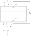
本実施の形態に係るオゾン生成装置は、図1に示すように、オゾン生成用素子10と、オゾン生成用素子10に交流電圧を印加する交流電源31と、を備える。オゾン生成用素子10は、長手方向と短手方向とを備える板形状であって、誘電体基板13と、一対の電極21A、21Bと、誘電体層12と、裏面電極25A、25Bと、プラグ26A、26Bと、を備える。以下、適宜図1におけるオゾン生成用素子10の厚さ方向をZ方向、Z方向において誘電体基板13から誘電体層12に向かう方向を+Z方向または上方とし、オゾン生成用素子10の厚さ方向に直交するオゾン生成用素子10の長手方向をX軸方向、Z軸方向およびX軸方向に直交するオゾン生成用素子10の短手方向をY軸方向として説明する。
誘電体基板13は、矩形板状の形状を有する。誘電体基板13の図1のY軸方向における両端部それぞれには、誘電体基板13を厚さ方向に貫通するコンタクトホール131A、131Bが形成されている。コンタクトホール131A、131B内には、それぞれプラグ26A、26Bが配されている。誘電体基板13は、CaO-B2O3-Al2O3-SiO2、Al2O3、SiO2、ZrO2、BaTiO3等の酸化物を含むセラミックス材料から形成されている。また、誘電体基板13は、LTCC(Low Temperature Co-fired Ceramics:低温同時焼結セラミックス)基板から形成されていてもよい。なお、誘電体基板13は、電気的絶縁性を有するものであればセラミックス材料に限定されるものではなく、エポキシ樹脂やポリイミド樹脂等の樹脂材料から形成されるものであってもよい。
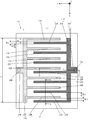
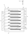
電極21A、21Bは、誘電体基板13の上面に設けられている。一対の電極21A、21Bは、図2に示すように、複数(図2では7本)の電極子部22A、22Bと、端子電極部23A、23Bと、舌片部24A、24Bと、を有する。電極21A、21Bは、Cu、Ag、Pd、Pt、W等の金属やRuO2のような導電性酸化物から形成されている。但し、オゾン生成用素子10の製造過程において焼成処理を行う場合、電極21A、21Bが金属であると、電極21A、21Bの焼成処理の際に誘電体基板13や誘電体層12へ拡散しうる。この場合、焼成処理において、誘電体基板13および誘電体層12の基となる誘電体材料の焼結が不十分となり誘電体基板13および誘電体層12の電圧耐性が低下する虞がある。従って、電極21A、21Bは、RuO2のような導電性酸化物から形成されていることが好ましい。また、電極21A、21Bの厚さは、10μm程度に設定される。なお、電極21A、21Bが本願発明の第1櫛形電極、第2櫛形電極に相当する。また、端子電極部23Aが本願発明の第1端子電極部に相当し、端子電極部23bが本願発明の第2端子電極部に相当する。電極子部22Aは本願発明の第1電極子部に相当し、電極子部22bが本願発明の第2電極子部に相当する。
複数の電極子部22A、22Bは、それぞれX軸方向に並んで配置されている。各電極子部22A、22Bは、長手方向と短手方向とを備える長細形状であり、端子電極部23A、23Bと交差してY軸方向に延びている。端子電極部23A(23B)は、長細形状であり、X軸方向に延びている。また、複数の電極子部22A(22B)は、端子電極部23A(23B)とともに、櫛形状の形状をなす。そして、電極21AのX軸方向で隣り合う2つの電極子部22Aの間に、電極21Bの電極子部22Bが配置されている。また、電極21BのX軸方向で隣り合う2つの電極子部22Bの間に、電極21Aの電極子部22Aが配置されている。即ち、一対の電極21A、21Bは、電極子部22Aと電極子部22BとがX軸方向に交互に並ぶように配置されたいわゆるインターディジタル型の構造を有する。
各電極子部22Bとその短手方向の一方側である+X方向側において隣り合って配置された電極子部22Aとの間の距離(第1距離)W11は、上記電極子部22Bとその短手方向の他方側である-X方向側において隣り合って配置された電極子部22Aとの間の距離(第2距離)W12と異なる。具体的には、距離W11は、距離W12に比べて短くなっている。距離W11は、隣り合う2つの電極子部22Aのうちの+X方向側の電極子部22Aと、それら2つの電極子部22Aの間に配置された電極子部22Bと、の間の距離に相当する。また、距離W12は、隣り合う2つの電極子部のうちの-X方向側の電極子部22Aと、それら2つの電極子部22Aの間に配置された電極子部22Bと、の間の距離に相当する。また、電極子部22A、22Bの線幅はW13である。
舌片部24Aは、端子電極部23AのX軸方向における中央部から-Y方向へ延出している。舌片部24Aは、コンタクトホール131A内に配されるプラグ26Aに電気的に接続される。舌片部24Bは、端子電極部23BのX軸方向における中央部から+Y方向へ延出している。舌片部24Bは、コンタクトホール131B内に配されるプラグ26Bに電気的に接続される。
誘電体層12は、図1に示すように、誘電体基板13の上面に設けられた電極21A、21Bを覆っている。誘電体層12は、CaO-B2O3-Al2O3-SiO2、Al2O3、SiO2、ZrO2、BaTiO3等の酸化物を含むセラミックス材料から形成されている。また、誘電体層12は、LTCC材から形成されていてもよい。なお、誘電体基板13は、電気的絶縁性を有するものであればセラミックス材料に限定されるものではなく、エポキシ樹脂やポリイミド樹脂等の樹脂材料から形成されるものであってもよい。但し、オゾン生成用素子10の動作時において、誘電体層12は、プラズマに曝されることにより高温になる。また、誘電体層12は、その表面近傍に生成したオゾンに曝されることからオゾンに対する耐浸食性も要求される。これらのことから、誘電体層12は、セラミックス材料から形成されていることが好ましい。また、誘電体層12は、その熱膨張率が誘電体基板13の熱膨張率と略等しい材料から形成されていることが好ましい。この場合、誘電体基板13と誘電体層12とがオゾン生成用素子10の動作時に生じる熱に起因して膨張および収縮した場合でも、誘電体基板13と誘電体層12との接合部分に歪みが生じにくい。従って、オゾン生成用素子10の動作時に生じる熱に起因した誘電体基板13と誘電体層12との接合部分の劣化が抑制されるという利点がある。更に、誘電体層12は、誘電体基板13と同一の材料から形成されていることがより好ましい。
裏面電極25A、25Bは、図3に示すように、誘電体基板13における誘電体層12側とは反対側の面において、少なくとも誘電体基板13のコンタクトホール131A、131Bを覆うように設けられている。プラグ26Aは、誘電体基板13のコンタクトホール131A内に配され、電極21Aと裏面電極25Aとを電気的に接続する。プラグ26Bは、誘電体基板13のコンタクトホール131B内に配され、電極21Bと裏面電極25Bとを電気的に接続する。裏面電極25A、25Bおよびプラグ26A、26Bは、電極21A、21Bと同様に、Cu、Ag、Pd、Pt、W等の金属やRuO2のような導電性材料から形成されている。
交流電源31は、裏面電極25A、25Bに電気的に接続され、一対の電極21A、21B間に交流電圧(正弦波電圧)を印加する。また、交流電源31は、周波数スイープ機能または共振周波数追従機能を有し、オゾン生成用素子10へ出力する交流電圧の周波数が交流電源31とオゾン生成用素子10とから構成される回路の共振周波数近傍となるように周波数を調整する。これにより上記回路での電力損失が低減される。なお、交流電源31は、矩形パルス列状の交流電圧を電極21A、21B間に印加するものであってもよい。
交流電源31からオゾン生成用素子10の一対の電極21A、21B間に交流電圧(正弦波電圧)が印加されると、誘電体層12の外表面近傍の各電極子部22A、22Bの間に位置する領域で沿面放電が生じる。放電現象は、空気中の絶縁破壊であり、各電極子部組22A、22Bの間に生じた電子が、各電極子部組22A、22Bの間に形成された電場のうち誘電体層12の外側に漏れ出ている成分により加速されることで発生する。同時に加速された電子は、誘電体層12の外表面近傍の各電極子部組22A、22Bの間に存在する酸素分子に衝突することによりオゾンが生成する。
次に、本実施の形態に係るオゾン生成用素子10について、放電開始電圧およびオゾン生成量を評価した結果について説明する。発明者らは、前述の本実施の形態に係るオゾン生成用素子10と後述する比較例に係るオゾン生成用素子とについて各評価を実施した。まず、発明者らが準備した評価用のオゾン生成用素子について説明する。
本実施の形態に係るオゾン生成用素子10として、図2に示す距離W12が55μm、65μm、75μm、100μm、125μm、150μm、200μmに設定された7種類を準備した。なお、これら7種類のオゾン生成用素子10は、全て電極子部22A、22BのX軸方向の幅が50μmであり、図2の距離W11が50μmである。また、誘電体基板13は平面視において10mm×10mmの正方形状であり、誘電体層12の厚さは15μmとした。そして、誘電体基板13と誘電体層12とを合わせた厚さは約600μmとした。更に、誘電体基板13上の電極21A、21Bにおける舌片部24A、24Bを除く部分が設けられる領域のX軸方向の長さL1を8mm、Y軸方向の長さL2を7mmとした。
図4に示すように、比較例に係るオゾン生成用素子910は、電極921Aの電極子部922Aと電極921Bの電極子部922Bとが交互に一定の間隔W91に配置されている。このオゾン生成用素子910として、図4に示す距離W91が50μmに設定されたものを準備した。なお、全ての電極子部922A、922BのX軸方向の幅は50μmである。また、誘電体基板13の形状、誘電体層12の厚さ、誘電体基板13と誘電体層12とを合わせた厚さ、誘電体基板13のうち、電極921A、921Bの複数の電極子部922A、922Bと端子電極部23A、23Bとが設けられる領域の寸法は、オゾン生成用素子10と同じとした。
次に、発明者らが、オゾン生成用素子10、910の放電開始電圧およびオゾン生成量を評価するために実施した放電開始電圧の測定およびオゾン生成量の測定の内容について説明する。放電開始電圧の測定では、オゾン生成用素子10の一対の電極21A、21B間またはオゾン生成用素子910の一対の電極921A、921B間に印加される交流電圧(正弦波電圧)の電圧振幅値を漸増させながら放電により生じるプラズマ発光の有無を観察した。プラズマ発光が観察された時点での電圧振幅値を放電開始電圧とした。
オゾン発生量の測定では、オゾン生成用素子10、910を容積が7リットルのアクリルケースの中に入れて、オゾン生成用素子10、910を3分間駆動したときのアクリルケース内のオゾン濃度をオゾン濃度計で測定した。ここにおいて、オゾン生成用素子10の一対の電極21A、21B間またはオゾン生成用素子910の一対の電極921A、921B間に、電圧振幅値2.3kVの交流電圧(正弦波電圧)を印加した。また、アクリルケース内にファンを設け、アクリルケース内の気体が攪拌されるようにした。オゾン濃度計は、荏原実業株式会社製の型式EG-3000を採用した。このオゾン発生量の測定では、実施の形態に係る7種類のオゾン生成用素子10と比較例に係るオゾン生成用素子910とをそれぞれ5個ずつ準備し、それぞれについて前述のようにしてオゾン濃度を測定した。
次に、オゾン生成用素子10、910について、放電開始電圧の測定と、オゾン生成量の測定と、を実施した結果について説明する。
放電開始電圧の測定では、実施の形態に係る7種類のオゾン生成用素子10と比較例に係るオゾン生成用素子910とのいずれについても、放電開始電圧の平均値が2.3kVであった。即ち、実施の形態に係るオゾン生成用素子10と比較例に係るオゾン生成用素子910とで、放電開始電圧に差異が確認されなかった。
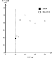
次に、オゾン生成用素子10、910についてオゾンの生成量の測定結果を図5に示す。図5では、横軸が図2に示す電極子部22A、22B間の距離W12であり、縦軸がオゾン濃度である。黒四角印は比較例に係るオゾン生成用素子910についての結果を示し、白四角印は実施の形態に係るオゾン生成用素子10についての結果を示している。オゾン生成用素子910の場合、オゾン濃度は39.50ppmであった。オゾン生成用素子10の場合、距離W12が55μm、65μm、75μm、100μm、125μm、150μm、200μmのものについて、オゾン濃度は、それぞれ、41.36ppm、40.65ppm、51.75ppm、55.19ppm、51.28ppm、49.53ppm、51.03ppmであった。この結果から、実施の形態に係るオゾン生成用素子10のオゾン濃度は、全て比較例に係るオゾン生成用素子910のオゾン濃度に比べて大きくなるという結果が得られた。即ち、電極子部22Bとその電極子部22Bの両側で隣り合う電極子部22Aそれぞれとの間の距離W11、W12、または、電極子部22Aとその電極子部22Aの両側で隣り合う電極子部22Bそれぞれとの間の距離W11、W12が互いに異なっているほうがオゾンの生成量が大きくなるという結果が得られた。特に、距離W12が75μm以上のオゾン生成用素子10で生成されるオゾンの濃度は、比較例に係るオゾン生成用素子910で生成されるオゾンの濃度に比べて約20%以上高くなるという結果も得られた。
図5に示す結果から、オゾン生成用素子10の距離W11に対する距離W12の比が、少なくとも1.1以上4.0以下であれば、比較例に係るオゾン生成用素子910に比べてオゾンの生成量が確実に増加することが判った。そして、オゾン生成用素子10の距離W11に対する距離W12の比が、1.5以上2.5以下であれば、比較例に係るオゾン生成用素子910に比べてオゾンの生成量が約20%以上増加することが判った。このことから、オゾン生成用素子10の距離W11に対する距離W12の比は、1.5以上2.5以下であることが好ましい。
次に、図5に示す実施の形態に係るオゾン生成用素子10と比較例に係るオゾン生成用素子910とでオゾンの生成量に差異が生じる理由について説明する。比較例に係るオゾン生成用素子910では、図6Aに示すように、電極子部922Aとその短手方向の他方側である-X方向で隣り合う電極子部922Bとの間の領域A91とその短手方向の一方側である+X方向で隣り合う電極子部922Bとの間の領域A92とで電場E91、E92が生じる。なお、図6Aでは、電極子部922Aの電位が電極子部922Bの電位よりも高い場合を示している。電場E91、E92の強さは領域A91、A92において同じである。電極子部922A、922B間での放電により領域A91、A92に生じた電子が、それぞれ電場E91、E92により加速されて誘電体層12近傍に存在する酸素分子に衝突することによりオゾンが発生する。なお、図6Aにおいて、V91は、領域A91において電場E91により加速される電子の加速度および加速方向を示す加速度ベクトルのX軸成分を示し、V92は、領域A92において電場E92により加速される電子の加速度および加速方向を示す加速度ベクトルのX軸成分を示す。
領域A91における電子の加速度ベクトルのX軸成分V91と領域A92における電子の加速度ベクトルのX軸成分V92の向きとが互いに逆になっている。また、隣り合う電極子部922A、922Bの間の距離は全て等しい。このため、領域A91、A92における電子の加速方向V91、V92の大きさは略同じになる。そうすると、例えば領域A91で+X方向へ加速された電子は、領域A92に入ると-X方向へ大きく減速されてしまう。特に、領域A91、A92の境界部分では、電場のX軸方向の成分が略ゼロとなり電子が加速されない領域となる。従って、比較例に係るオゾン生成用素子910では、電子に大きなエネルギを与えることができず、その分、オゾンの生成効率が低い。
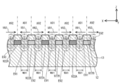
これに対して、本実施の形態に係るオゾン生成用素子10では、図6Bに示すように、電極子部22Aとその短手方向の他方側である-X方向で隣り合う電極子部22Bとの間の領域A1の電場E1は、電極子部22Aとその短手方向の一方側である+X方向で隣り合う電極子部22Bとの間の領域A2の電場E2に比べて強くなっている。なお、図6Bにおいて、V1は、領域A1において電場E1により加速される電子の加速度および加速方向を示す加速度ベクトルのX軸成分を示し、V2は、領域A2において電場E2により加速される電子の加速度および加速方向を示す加速度ベクトルのX軸成分を示す。図6Bに示すように、領域A1における電子の加速度ベクトルのX軸成分V1の大きさは、領域A2における電子の加速度ベクトルのX軸成分V2の大きさに比べて大きくなる。そうすると、例えば領域A1で+X方向へ加速された電子は、領域A2においてほとんど減速されず、その領域A2の+X方向で隣り合う他の領域A1で更に+X方向へ加速される。その結果、電子は大きなエネルギを持つことになる。このように、実施の形態に係るオゾン生成用素子10では、電子に比較的大きなエネルギを与えることができるので、その分、オゾンの生成効率が高い。
オゾン生成用素子10、910では、それらの動作時に発する熱により生成されたオゾンの一部が分解され、実効的なオゾン発生量が減少する。オゾン生成用素子910の場合、オゾン生成用素子910を冷却することにより、オゾンの分解による減少を抑制する必要がある。これに対して、オゾン生成用素子10は、前述のようにオゾン生成用素子910に比べてオゾンの生成効率が高く、その動作時に発する熱によるオゾンの分解によるオゾンの減少分を相殺するだけのオゾンを発生しうる。
一方、オゾン生成用素子10の電極子部22A、22B間の距離W12が極端に長い(例えば距離W11に対する距離W12の比が4.0を超える場合)と、電極子部22A、22Bの密度もそれに伴い減少する。すると、オゾンの生成源となる電極子部22A、22Bの密度減少により生成されるオゾン量が減少してしまう。従って、オゾン生成用素子10について、距離W11に対する距離W12の比に前述のような最適範囲(1.5以上2.5以下)が存在すると考えられる。
更に、実施の形態に係るオゾン生成用素子10の電極子部22A、22Bの数は、比較例に係るオゾン生成用素子910の電極子部922A、922Bの数よりも少ない。これにより、オゾン生成用素子10の電極21A、21B間の静電容量は、オゾン生成用素子910の電極921A、921B間の静電容量に比べて小さくなる。そうすると、交流電源31の負荷が小さくなるため、交流電源31を小型化することができる。
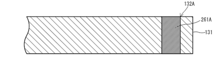
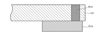
次に、本実施の形態に係るオゾン生成用素子10の製造方法の一例について図7A乃至図7D、図8Aおよび図8Bを参照しながら説明する。なお、図7A乃至図7D、図8Aおよび図8Bは、図2のB-B線におけるオゾン生成用素子10の断面矢視図に対応する各工程での断面図である。この製造方法では、まず、誘電体基板13および誘電体層12の基となる誘電体シートを形成し、次に、誘電体シートに電極21A、21B等の基となる金属ペーストパターンを形成する。その後、誘電体シートを積層してから、誘電体シートの積層体を焼成してオゾン生成用素子10を作製する。
まず、誘電体基板13および誘電体層12の基となる誘電体シート(いわゆるセラミックスグリーンシート)を形成する。詳細には、まず、CaO-B2O3-Al2O3-SiO2ガラスと、Al2O3と、トルエンとエタノールとの混合溶媒と、分散剤と、バインダと、を、ボールミルを用いて粉砕および混合することにより、スラリーを作製する。次に、ドクターブレード法により、得られたスラリーから誘電体シートを作製する。なお、シート形成工程で使用する材料は、前述の材料を含むものに限定されるものではなく、CaO-B2O3-Al2O3-SiO2ガラス以外の他の種類のガラスやSiO2、ZrO2、BaTiO3等の酸化物を含むものであってもよい。或いは、誘電体基板13および誘電体層12がエポキシ樹脂やポリイミド樹脂等の樹脂材料から形成される場合、シート形成工程においてエポキシ樹脂やポリイミド樹脂等の樹脂材料が使用されてもよい。
次に、誘電体基板13に使用する複数の誘電体シートにプラグ26A、26Bの基となる金属ペースト充填部を形成する。詳細には、図7Aに示すように、メカパンチャ等の穿孔装置を用いて、誘電体シート131に厚さ方向に貫通する貫通孔132Aを形成する。貫通孔132Aは、誘電体シート131が積層されたときに相対的に同一の位置となるように形成される。次に、図7Bに示すように、誘電体シート131の各貫通孔132AにAgペーストが充填される。これにより、誘電体シート131に金属ペースト充填部261Aが形成される。
続いて、スクリーン印刷技術を利用して、図7Cに示すように誘電体基板13の最上層に配置される誘電体シートに電極21A、21Bの基となる第1金属ペーストパターン211A、211Bを形成する。また、スクリーン印刷技術を利用して、図7Dに示すように誘電体基板13に使用する複数の誘電体シートのうち、誘電体基板13の最下層に配置される誘電体シートに裏面電極25A、25Bの基となる第2金属ペーストパターン251Aを形成する。第1金属ペーストパターン211A、211Bおよび第2金属ペーストパターン251Aは、RuO2ペーストからなる。
その後、まず、図8Aに示すように、誘電体基板13に使用する複数の誘電体シート131を積層するとともに誘電体基板13の最上部に配置される誘電体シート131上に誘電体層12の基となる1枚の誘電体シート121を積層する。次に、圧着機により誘電体シート121、131を圧着し積層体を得る。
続いて、得られた積層体を焼成温度900℃で焼成する。図8Bに示すように、誘電体シート121、131が焼結して誘電体層12、132が形成される。また、金属ペースト充填部261A、第1金属ペーストパターン211A、211Bおよび第2金属ペーストパターン251Aが焼結して導電部262A、電極21A、21Bおよび裏面電極25Aが形成される。
このオゾン生成用素子10の製造方法は、前述のように他の工程に比べて比較的手間がかかる焼成工程の回数が1回だけである。従って、オゾン生成用素子10の製造に携わる作業者の負担が軽減されるという利点がある。
以上説明したように、本実施の形態に係るオゾン生成用素子10は、距離W11が距離W12と異なる。これにより、オゾン生成用素子10は、比較例に係るオゾン生成用素子910に比べて、電極21A、21Bの電極子部22A、22B間に生じる電場から電極子部22A、22B間での放電により生じた電子に与えられるエネルギが高まるのでオゾンの生成がより活発化する。従って、本実施の形態に係るオゾン生成用素子10は、比較例に係るオゾン生成用素子910と比べて、オゾンの生成効率が高く、動作時に発する熱によるオゾンの分解によるオゾンの減少分を相殺するだけのオゾンを発生しうる。そして、オゾン生成用素子10はオゾン生成用素子910と同等以上のオゾン発生量を確保しうる。故に、オゾン生成用素子10は、誘電体基板13の厚みを厚くしたり、冷却器とともに使用したりする必要がないので、オゾン生成用素子10或いはオゾン生成用素子10を含むモジュール全体を小型化することができる。
また、本実施の形態に係るオゾン生成用素子10において、距離W11に対する距離W12の比が1.5以上2.5以下のものは、比較例に係るオゾン生成用素子910に比べてオゾンの生成効率が約20%以上高くなるという利点がある。
更に、本実施の形態に係るオゾン生成用素子10では、誘電体層12が誘電体基板13の電極21A、21Bが形成された一面を覆っている。これにより、電極21A、21Bが生成されたオゾンに曝されることがないので、電極21A、21Bの劣化が抑制されるという利点がある。
[変形例]
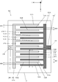
以上、本発明の実施の形態について説明したが、本発明は前述の実施の形態の構成に限定されるものではない。例えば、図9に示す変形例1に係るオゾン生成用素子210のように、電極子部222A、222Bが誘電体基板213の裏面に設けられた裏面電極228A、228Bにプラグ227A、227Bを介して電気的に接続されている構成であってもよい。ここにおいて、複数の電極子部222Aと複数のプラグ227Aとから裏面電極228Aに電気的に接続された電極221Aが構成され、複数の電極子部222Bと複数のプラグ227Bとから裏面電極228Bに電気的に接続された電極221Bが構成されている。
以上、本発明の実施の形態について説明したが、本発明は前述の実施の形態の構成に限定されるものではない。例えば、図9に示す変形例1に係るオゾン生成用素子210のように、電極子部222A、222Bが誘電体基板213の裏面に設けられた裏面電極228A、228Bにプラグ227A、227Bを介して電気的に接続されている構成であってもよい。ここにおいて、複数の電極子部222Aと複数のプラグ227Aとから裏面電極228Aに電気的に接続された電極221Aが構成され、複数の電極子部222Bと複数のプラグ227Bとから裏面電極228Bに電気的に接続された電極221Bが構成されている。
本構成によれば、オゾン生成用素子210の上面において電極子部が省略されている分、オゾン生成用素子210の上面の面積の縮小が図れる。従って、オゾン生成用素子210の小型化を図ることができる。
前述の実施の形態では、各電極子部22Bとその短手方向の他方側である-X方向に隣り合って配置された電極子部22Aとの間の距離W12が互いに等しい例について説明した。但し、これに限らず、例えば図10に示す変形例2に係るオゾン生成用素子310のように、電極子部22Bとその電極子部22Bの短手方向の他方側である-X方向に隣り合って配置された電極子部22Aとの間の距離W321、W322、W323が互いに異なっていてもよい。オゾン生成用素子310では、電極子部22Bとその電極子部22Bの-X方向に配置された電極子部22Aとの間の距離W321、W322、W323が+X方向側ほど大きくなっている。
本構成によれば、オゾン生成用素子310における電極子部22A、22Bの密度が低い部分(-X方向側)の温度は、電極子部22A、22Bの密度が高い部分(+X方向側)の温度に比べて低くなる。従って、オゾン生成用素子310は、例えばその+X方向側だけがヒートシンクに接触させた状態で使用されてもオゾン生成用素子310全体の温度が低下する。これにより、オゾン生成用素子310の誘電体層12近傍でのオゾン分解が抑制される。従って、ヒートシンクを小型化しつつ、オゾン生成用素子310でのオゾンの生成量を比較的高い水準で維持することが可能となる。
実施の形態では、誘電体基板13と誘電体層12とが熱膨張率の略等しい材料から形成される例について説明したが、これに限らず、誘電体基板13と誘電体層12とが熱膨張率の異なる材料から形成されていてもよい。
実施の形態では、誘電体層12を備える構成について説明したが、これに限らず、誘電体層12を備えない構成であってもよい。
各実施の形態では、交流電源31が裏面電極25A、25Bと電気的に接続される構成について説明したが、これに限らず、交流電源31が、裏面電極25A、25Bでなく、誘電体基板13の表面に設けられた電極21A、21Bの一部(例えば舌片部24A、24B)と電気的に接続される構成であってもよい。
各実施の形態では、電極21A、21Bがプラグ26A、26Bを介して裏面電極25A、25Bに接続される構成について説明したが、これに限らず、例えば電極21A、21Bがプラグを介して誘電体基板13の端面に設けられた取り出し用電極(図示せず)に接続される構成であってもよい。
実施の形態に係るオゾン生成用素子10の製造方法は、前述の実施形態で説明した製造方法に限定されるものではない。例えば予め誘電体シート131を積層したものを焼成することにより誘電体基板13を準備しておく方法であってもよい。この場合、準備した誘電体基板13の上面に電極21A、21Bを形成し、その後、誘電体基板13の上面にガラスペーストを印刷することにより誘電体層12を形成するものでもよい。或いは、第1金属ペーストパターン211A、211B等が形成された誘電体シート131と金属ペースト充電部261Aが形成された誘電体シート131を積層して焼成することにより、電極21A、21Bが設けられた誘電体基板13を準備する方法でもよい。この場合、準備した電極21A、21Bが設けられた誘電体基板13の上面に誘電体層12を別途形成する。
以上、本発明の実施の形態および変形例(なお書きに記載したものを含む。以下、同様。)について説明したが、本発明はこれらに限定されるものではない。本発明は、実施の形態および変形例が適宜組み合わされたもの、それに適宜変更が加えられたものを含む。
本出願は、2016年3月9日に出願された日本国特許出願特願2016-045478号に基づく。本明細書中に日本国特許出願特願2016-045478号の明細書、特許請求の範囲および図面全体を参照として取り込むものとする。
10,210,310:オゾン生成用素子、12,132:誘電体層、13,213:誘電体基板、21A,21B,221A,221B,321A,321B:電極、22A,22B,222A,222B:電極子部、23A,23B:電極子部、24A,24B:舌片部、25A,25B,228A,228B:裏面電極、26A,26B,227A,227B:プラグ、31:交流電源、121,131:誘電体シート、131A,131B:コンタクトホール、132A:貫通孔、211A,211B:第1金属ペーストパターン、251A:第2金属ペーストパターン、261A:金属ペースト充電部、262A:導電部、A1,A2:領域、E1,E2:電場
Claims (5)
- 誘電体基板と、
前記誘電体基板の一方主面に設けられた第1櫛形電極と第2櫛形電極とを備え、
前記第1櫛形電極は、第1端子電極部と、前記第1端子電極部と交差する複数の第1電極子部とを有し、
前記第2櫛形電極は、第2端子電極部と、前記第2端子電極部と交差する複数の第2電極子部とを有し、
前記第1電極子部と前記第2電極子部とは一方向に交互に並ぶように配置されており、
前記第1電極子部と、前記第1電極子部と一方向側において隣り合う第2電極子部との間隔である第1距離は、前記第1電極子部と、前記第1電極子部と他方向側において隣り合う第2電極子部との間隔である第2距離と異なり、
前記第1距離に対する前記第2距離の比は、1.1以上4.0以下である、
オゾン生成用素子。 - 前記第1距離に対する前記第2距離の比は、1.5以上2.5以下である、
請求項1に記載のオゾン生成用素子。 - 前記誘電体基板の前記一方主面を覆う誘電体層を更に備える、
請求項1または2に記載のオゾン生成用素子。 - 前記第1電極子部と前記第2電極子部とは、それぞれ、前記第1端子電極部、前記第2端子電極部に連なっている、
請求項1から3のいずれか1項に記載のオゾン生成用素子。 - 請求項1から4のいずれか1項に記載のオゾン生成用素子と、
前記第1櫛形電極と前記第2櫛形電極の間に交流電圧を印加する交流電源と、を備える、
オゾン生成装置。
Priority Applications (3)
| Application Number | Priority Date | Filing Date | Title |
|---|---|---|---|
| DE112017001230.9T DE112017001230B4 (de) | 2016-03-09 | 2017-01-12 | Ozongenerierungs-Bauelement und Ozongenerierungsvorrichtung |
| JP2018504022A JP6610771B2 (ja) | 2016-03-09 | 2017-01-12 | オゾン生成用素子およびオゾン生成装置 |
| CN201780015391.6A CN108712997B (zh) | 2016-03-09 | 2017-01-12 | 臭氧生成用元件以及臭氧生成装置 |
Applications Claiming Priority (2)
| Application Number | Priority Date | Filing Date | Title |
|---|---|---|---|
| JP2016-045478 | 2016-03-09 | ||
| JP2016045478 | 2016-03-09 |
Publications (1)
| Publication Number | Publication Date |
|---|---|
| WO2017154337A1 true WO2017154337A1 (ja) | 2017-09-14 |
Family
ID=59790173
Family Applications (1)
| Application Number | Title | Priority Date | Filing Date |
|---|---|---|---|
| PCT/JP2017/000752 Ceased WO2017154337A1 (ja) | 2016-03-09 | 2017-01-12 | オゾン生成用素子およびオゾン生成装置 |
Country Status (4)
| Country | Link |
|---|---|
| JP (1) | JP6610771B2 (ja) |
| CN (1) | CN108712997B (ja) |
| DE (1) | DE112017001230B4 (ja) |
| WO (1) | WO2017154337A1 (ja) |
Families Citing this family (1)
| Publication number | Priority date | Publication date | Assignee | Title |
|---|---|---|---|---|
| CN115594152B (zh) * | 2021-07-09 | 2024-07-09 | 财团法人工业技术研究院 | 臭氧产生装置以及臭氧产生方法 |
Citations (5)
| Publication number | Priority date | Publication date | Assignee | Title |
|---|---|---|---|---|
| JPH09286604A (ja) * | 1996-04-19 | 1997-11-04 | Toshiba Fa Syst Eng Kk | 放電処理装置 |
| JPH10245204A (ja) * | 1997-03-03 | 1998-09-14 | Toshiba Fa Syst Eng Kk | ガス放電装置 |
| JP2000072410A (ja) * | 1998-08-25 | 2000-03-07 | Toshiba Fa Syst Eng Corp | オゾン発生装置 |
| JP2001302215A (ja) * | 2000-04-21 | 2001-10-31 | Toshiba Fa Syst Eng Corp | オゾン発生装置 |
| JP2003089506A (ja) * | 2001-09-14 | 2003-03-28 | Toshiba Corp | オゾン発生装置 |
Family Cites Families (8)
| Publication number | Priority date | Publication date | Assignee | Title |
|---|---|---|---|---|
| RU2064890C1 (ru) * | 1993-11-26 | 1996-08-10 | Сергей Булигенович Акпанбетов | Способ получения озона и его генератор |
| CN2255425Y (zh) * | 1996-06-14 | 1997-06-04 | 清华大学 | 高效高浓度臭氧发生装置 |
| US20040197244A1 (en) * | 2003-04-03 | 2004-10-07 | Alan Kirby | Corona discharge plate electrode ozone generator |
| CN2609911Y (zh) * | 2003-04-16 | 2004-04-07 | 薛荃 | 臭氧发生器 |
| JP4208732B2 (ja) | 2004-02-02 | 2009-01-14 | 株式会社東芝 | オゾン発生ユニット及びオゾン発生装置 |
| JP4709712B2 (ja) * | 2006-08-24 | 2011-06-22 | 株式会社東芝 | オゾン発生装置 |
| CN202322375U (zh) * | 2011-11-10 | 2012-07-11 | 上海康特环保科技发展有限公司 | 一种臭氧发生片 |
| JP6354456B2 (ja) | 2014-08-27 | 2018-07-11 | 京セラドキュメントソリューションズ株式会社 | 電子機器および表示プログラム |
-
2017
- 2017-01-12 DE DE112017001230.9T patent/DE112017001230B4/de active Active
- 2017-01-12 CN CN201780015391.6A patent/CN108712997B/zh active Active
- 2017-01-12 WO PCT/JP2017/000752 patent/WO2017154337A1/ja not_active Ceased
- 2017-01-12 JP JP2018504022A patent/JP6610771B2/ja active Active
Patent Citations (5)
| Publication number | Priority date | Publication date | Assignee | Title |
|---|---|---|---|---|
| JPH09286604A (ja) * | 1996-04-19 | 1997-11-04 | Toshiba Fa Syst Eng Kk | 放電処理装置 |
| JPH10245204A (ja) * | 1997-03-03 | 1998-09-14 | Toshiba Fa Syst Eng Kk | ガス放電装置 |
| JP2000072410A (ja) * | 1998-08-25 | 2000-03-07 | Toshiba Fa Syst Eng Corp | オゾン発生装置 |
| JP2001302215A (ja) * | 2000-04-21 | 2001-10-31 | Toshiba Fa Syst Eng Corp | オゾン発生装置 |
| JP2003089506A (ja) * | 2001-09-14 | 2003-03-28 | Toshiba Corp | オゾン発生装置 |
Also Published As
| Publication number | Publication date |
|---|---|
| DE112017001230B4 (de) | 2024-10-02 |
| CN108712997B (zh) | 2021-11-30 |
| DE112017001230T5 (de) | 2018-12-13 |
| JPWO2017154337A1 (ja) | 2018-09-20 |
| CN108712997A (zh) | 2018-10-26 |
| JP6610771B2 (ja) | 2019-11-27 |
Similar Documents
| Publication | Publication Date | Title |
|---|---|---|
| US9595386B2 (en) | Multilayer ceramic electronic component and board having the same mounted thereon | |
| US20130119264A1 (en) | Ion Wind Generator and Ion Wind Generating Device | |
| KR20160131879A (ko) | 감전 방지 소자 및 이를 구비하는 전자기기 | |
| JP5795065B2 (ja) | プラズマ発生体及びプラズマ発生装置 | |
| JP5774960B2 (ja) | プラズマ発生体及びプラズマ発生装置 | |
| JP6610771B2 (ja) | オゾン生成用素子およびオゾン生成装置 | |
| US9036325B2 (en) | Ion wind generator and ion wind generating device | |
| JP6167445B2 (ja) | プラズマ発生体及びプラズマ発生装置 | |
| JPS6114103A (ja) | セラミツクを用いたオゾナイザ− | |
| JP5757372B2 (ja) | Esd保護デバイス | |
| JP6627963B2 (ja) | オゾン生成用素子およびオゾン生成装置 | |
| JP5668134B2 (ja) | イオン風発生体及びイオン風発生装置 | |
| JP6033651B2 (ja) | プラズマ発生体及びプラズマ発生装置 | |
| KR101253345B1 (ko) | 이온 발생 장치 및 그의 제조방법 | |
| JP6354865B2 (ja) | オゾン生成装置 | |
| JP6547826B2 (ja) | オゾン生成装置 | |
| JP6350680B2 (ja) | オゾン生成装置 | |
| JP5638362B2 (ja) | イオン風発生体及びイオン風発生装置 | |
| JP2013085005A (ja) | 放電ギャップパターン及び電源装置 | |
| JP2020025044A (ja) | セラミック配線基板 | |
| KR20170126840A (ko) | 적층형 소자 및 이를 구비하는 전자기기 |
Legal Events
| Date | Code | Title | Description |
|---|---|---|---|
| ENP | Entry into the national phase |
Ref document number: 2018504022 Country of ref document: JP Kind code of ref document: A |
|
| 121 | Ep: the epo has been informed by wipo that ep was designated in this application |
Ref document number: 17762684 Country of ref document: EP Kind code of ref document: A1 |
|
| 122 | Ep: pct application non-entry in european phase |
Ref document number: 17762684 Country of ref document: EP Kind code of ref document: A1 |