WO2017154228A1 - 超電導線及びその製造方法 - Google Patents
超電導線及びその製造方法 Download PDFInfo
- Publication number
- WO2017154228A1 WO2017154228A1 PCT/JP2016/065124 JP2016065124W WO2017154228A1 WO 2017154228 A1 WO2017154228 A1 WO 2017154228A1 JP 2016065124 W JP2016065124 W JP 2016065124W WO 2017154228 A1 WO2017154228 A1 WO 2017154228A1
- Authority
- WO
- WIPO (PCT)
- Prior art keywords
- superconducting wire
- superconducting
- reinforcing layer
- layer
- surface side
- Prior art date
- Legal status (The legal status is an assumption and is not a legal conclusion. Google has not performed a legal analysis and makes no representation as to the accuracy of the status listed.)
- Ceased
Links
Images











Classifications
-
- H—ELECTRICITY
- H01—ELECTRIC ELEMENTS
- H01F—MAGNETS; INDUCTANCES; TRANSFORMERS; SELECTION OF MATERIALS FOR THEIR MAGNETIC PROPERTIES
- H01F6/00—Superconducting magnets; Superconducting coils
- H01F6/06—Coils, e.g. winding, insulating, terminating or casing arrangements therefor
-
- H—ELECTRICITY
- H01—ELECTRIC ELEMENTS
- H01B—CABLES; CONDUCTORS; INSULATORS; SELECTION OF MATERIALS FOR THEIR CONDUCTIVE, INSULATING OR DIELECTRIC PROPERTIES
- H01B12/00—Superconductive or hyperconductive conductors, cables, or transmission lines
- H01B12/02—Superconductive or hyperconductive conductors, cables, or transmission lines characterised by their form
- H01B12/06—Films or wires on bases or cores
-
- H—ELECTRICITY
- H01—ELECTRIC ELEMENTS
- H01B—CABLES; CONDUCTORS; INSULATORS; SELECTION OF MATERIALS FOR THEIR CONDUCTIVE, INSULATING OR DIELECTRIC PROPERTIES
- H01B13/00—Apparatus or processes specially adapted for manufacturing conductors or cables
-
- H—ELECTRICITY
- H01—ELECTRIC ELEMENTS
- H01R—ELECTRICALLY-CONDUCTIVE CONNECTIONS; STRUCTURAL ASSOCIATIONS OF A PLURALITY OF MUTUALLY-INSULATED ELECTRICAL CONNECTING ELEMENTS; COUPLING DEVICES; CURRENT COLLECTORS
- H01R4/00—Electrically-conductive connections between two or more conductive members in direct contact, i.e. touching one another; Means for effecting or maintaining such contact; Electrically-conductive connections having two or more spaced connecting locations for conductors and using contact members penetrating insulation
- H01R4/58—Electrically-conductive connections between two or more conductive members in direct contact, i.e. touching one another; Means for effecting or maintaining such contact; Electrically-conductive connections having two or more spaced connecting locations for conductors and using contact members penetrating insulation characterised by the form or material of the contacting members
- H01R4/68—Connections to or between superconductive connectors
-
- H—ELECTRICITY
- H01—ELECTRIC ELEMENTS
- H01R—ELECTRICALLY-CONDUCTIVE CONNECTIONS; STRUCTURAL ASSOCIATIONS OF A PLURALITY OF MUTUALLY-INSULATED ELECTRICAL CONNECTING ELEMENTS; COUPLING DEVICES; CURRENT COLLECTORS
- H01R43/00—Apparatus or processes specially adapted for manufacturing, assembling, maintaining, or repairing of line connectors or current collectors or for joining electric conductors
-
- H—ELECTRICITY
- H01—ELECTRIC ELEMENTS
- H01R—ELECTRICALLY-CONDUCTIVE CONNECTIONS; STRUCTURAL ASSOCIATIONS OF A PLURALITY OF MUTUALLY-INSULATED ELECTRICAL CONNECTING ELEMENTS; COUPLING DEVICES; CURRENT COLLECTORS
- H01R43/00—Apparatus or processes specially adapted for manufacturing, assembling, maintaining, or repairing of line connectors or current collectors or for joining electric conductors
- H01R43/02—Apparatus or processes specially adapted for manufacturing, assembling, maintaining, or repairing of line connectors or current collectors or for joining electric conductors for soldered or welded connections
-
- Y—GENERAL TAGGING OF NEW TECHNOLOGICAL DEVELOPMENTS; GENERAL TAGGING OF CROSS-SECTIONAL TECHNOLOGIES SPANNING OVER SEVERAL SECTIONS OF THE IPC; TECHNICAL SUBJECTS COVERED BY FORMER USPC CROSS-REFERENCE ART COLLECTIONS [XRACs] AND DIGESTS
- Y02—TECHNOLOGIES OR APPLICATIONS FOR MITIGATION OR ADAPTATION AGAINST CLIMATE CHANGE
- Y02E—REDUCTION OF GREENHOUSE GAS [GHG] EMISSIONS, RELATED TO ENERGY GENERATION, TRANSMISSION OR DISTRIBUTION
- Y02E40/00—Technologies for an efficient electrical power generation, transmission or distribution
- Y02E40/60—Superconducting electric elements or equipment; Power systems integrating superconducting elements or equipment
Definitions
- the present invention relates to a superconducting wire and a method for manufacturing the same.
- This application claims priority based on Japanese Patent Application No. 2016-48786 filed on March 11, 2016, and incorporates all the content described in the above Japanese application.
- the superconducting wire is lengthened by sequentially connecting a plurality of superconducting wires.
- Patent Document 1 As a structure for connecting a plurality of superconducting wires, a connection structure described in JP 2011-238513 A (Patent Document 1) has been proposed.
- the first superconducting wire described in Patent Document 1 has a superconducting layer, an internal solder layer, and a reinforcing layer. Moreover, the superconducting wire described in Patent Document 1 has a terminal portion.
- the second superconducting wire described in Patent Document 1 has the same structure as the first superconducting wire.
- the superconducting layer has a first surface and a second surface.
- the reinforcing layer is provided on the first surface and the second surface. However, the reinforcing layer is not provided on the region located on the terminal portion side of the first surface. That is, the superconducting layer is exposed in the region located on the terminal portion side of the first surface.
- the internal solder layer is provided between the reinforcing layer and the first surface and the second surface, and joins the reinforcing layer and the superconducting layer.
- the connection structure of the superconducting wire described in Patent Document 1 has a first superconducting wire, a second superconducting member, and a connecting solder layer.
- the superconducting layer exposed in the region located on the terminal portion side of the first surface of the second superconducting member is exposed in the region located on the terminal portion side of the first surface of the first superconducting member.
- a superconducting layer exposed in a region located on the terminal portion side of the first surface of the first superconducting member, and a superconducting layer exposed in a region located on the terminal portion side of the first surface of the second superconducting member; Are joined by connecting solder.
- the superconducting wire of the present disclosure is a first superconducting wire having a first surface and a first back surface that is a surface opposite to the first surface, a second surface, and a surface opposite to the second surface.
- the first superconducting wire has a first superconducting layer and a first reinforcing layer provided on the first surface side and the first back surface side of the first superconducting layer.
- the second superconducting wire has a second superconducting layer and a second reinforcing layer provided on the second front surface side and the second back surface side of the second superconducting layer.
- the first superconducting wire has a first end from which at least a part of the first reinforcing layer on the first surface side is removed.
- the second superconducting wire has a second end from which at least a part of the second reinforcing layer on the second surface side is removed.
- the first surface located at the first end is joined to the second surface located other than the second end by the connecting member, and the second surface located at the second end is joined by the connecting member, It is joined to the first surface located other than the first end.
- the joint structure of the superconducting wire described in Patent Document 1 may not have sufficient mechanical properties when subjected to bending deformation, tensile deformation, or the like. That is, in the superconducting wire joint structure described in Patent Document 1, when subjected to bending deformation, tensile deformation, etc., stress concentration tends to occur at the ends of the portions where the superconducting layers face each other via the connecting solder. .
- the present disclosure has been made in view of such problems of the prior art. That is, the present disclosure provides a superconducting wire having excellent mechanical characteristics.
- a superconducting wire includes a first superconducting wire having a first surface, a first back surface opposite to the first surface, a second surface, and a second surface.
- a second superconducting wire having a second back surface opposite to the front surface; and a connecting member for joining the first superconducting wire and the second superconducting wire.
- the first superconducting wire has a first superconducting layer and a first reinforcing layer provided on the first surface side and the first back surface side of the first superconducting layer.
- the second superconducting wire has a second superconducting layer and a second reinforcing layer provided on the second front surface side and the second back surface side of the second superconducting layer.
- the first superconducting wire has a first end from which at least a part of the first reinforcing layer on the first surface side is removed.
- the second superconducting wire has a second end from which at least a part of the second reinforcing layer on the second surface side is removed.
- the first surface located at the first end is joined to the second surface located other than the second end by the connecting member, and the second surface located at the second end is joined by the connecting member, It is joined to the first surface located other than the first end.
- the superconducting wire (1) it becomes possible to obtain good mechanical properties against bending deformation, tensile deformation and the like.
- the superconducting wire (2) it is possible to reduce the connection resistance value between the first superconducting wire and the second superconducting wire.
- the superconducting wires of (1) and (2) include a conductive member having an electric resistance value lower than that of the connection member, and the conductive member includes a first surface located at the first end and a second surface. It arrange
- the superconducting wire (3) it is possible to reduce the connection resistance value between the first superconducting wire and the second superconducting wire.
- the superconducting wires of (1) to (3) further include a first reinforcing member provided on the first reinforcing layer on the first back surface side, and the first reinforcing member is a first reinforcing member. You may protrude from an edge part and may be joined to the 2nd reinforcement layer of the 2nd surface side.
- the superconducting wires of (1) to (4) further include a second reinforcing member provided on the second reinforcing layer on the second back surface side, and the second reinforcing member is the second reinforcing member. You may protrude from an edge part and may be joined to the 1st reinforcement layer of the 1st surface side.
- the superconducting wires of (1) to (5) have an allowable tensile strength of 80% or more of the smaller allowable tensile strength of the first superconducting wire and the second superconducting wire. It may be.
- the superconducting wires of (1) to (6) have an allowable bending diameter that is not more than four times the larger allowable bending diameter of the first superconducting wire and the second superconducting wire. It may be.
- a superconducting wire according to an embodiment of the present invention includes a first superconducting wire having a first surface, a first back surface opposite to the first surface, a second surface, and a second surface.
- a second superconducting wire having a second back surface opposite to the front surface; and a connecting member for joining the first superconducting wire and the second superconducting wire.
- the first superconducting wire has a first superconducting layer and a first reinforcing layer provided on the first surface side and the first back surface side of the first superconducting layer.
- the second superconducting wire has a second superconducting layer and a second reinforcing layer provided on the second front surface side and the second back surface side of the second superconducting layer.
- the first superconducting wire has a first end from which at least a part of the first reinforcing layer on the first surface side is removed.
- the second superconducting wire has a second end from which at least a part of the second reinforcing layer on the second surface side is removed.
- the first surface located at the first end and the second surface located at the second end are joined by a connecting member.
- the first reinforcing layer on the first back surface side has a first protruding portion that protrudes from the first end and is joined to the second reinforcing layer on the second surface side.
- the second reinforcing layer on the second back surface side has a second protruding portion that protrudes from the second end portion and is joined to the first reinforcing layer on the first surface side.
- a superconducting wire includes a first superconducting wire having a first surface, a first back surface that is a surface opposite to the first surface, a second surface, and a second surface.
- a second superconducting wire having a second back surface opposite to the front surface, a third reinforcing member disposed between the first surface and the second surface, the first superconducting wire, and a third And a connecting member that joins the second superconducting wire and the third reinforcing member.
- the 1st superconducting wire has the 1st superconducting layer and the 1st reinforcement layer provided in the 1st surface side and the 1st back side of the 1st superconducting layer.
- the first superconducting wire has a first end from which at least a part of the first reinforcing layer on the first surface side is removed.
- the second superconducting wire has a second superconducting layer and a second reinforcing layer provided on the second front surface side and the second back surface side of the second superconducting layer.
- the second superconducting wire has a second end from which at least a part of the second reinforcing layer on the second surface side is removed.
- the first surface located at the first end is disposed so as to face the second surface located other than the second end, and the second surface located at the second end is defined as the first end. It arrange
- the third reinforcing member has a lower electrical resistance value than the connecting member and a higher strength than the connecting member.
- the superconducting wire of (10) it becomes possible to obtain better mechanical characteristics against bending deformation, tensile deformation, etc., and the connection resistance value between the first superconducting wire and the second superconducting wire is reduced. It becomes possible to do.
- the superconducting wire of (11) it is possible to reduce the connection resistance value between the first superconducting wire and the second superconducting wire.
- the first reinforcing layer causes compressive strain to the first superconducting layer
- the second reinforcing layer is the second superconducting layer. Compressive strain may be generated.
- the compressive strain with respect to the first superconducting layer located at the first end is smaller than the compressive strain with respect to the first superconducting layer located outside the first end
- the compressive strain for the second superconducting layer located at the second end may be smaller than the compressive strain for the second superconducting layer located other than the second end.
- a method of manufacturing a superconducting wire according to an embodiment of the present invention includes a first superconducting wire having a first surface and a first back surface that is a surface opposite to the first surface, and a second surface. And a step of joining to a second superconducting wire having a second back surface that is a surface opposite to the second surface.
- the first superconducting wire has a first superconducting layer and a first reinforcing layer provided on the first front surface side and the first back surface side.
- the second superconducting wire has a second superconducting layer and a second reinforcing layer provided on the second front surface side and the second back surface side.
- the first superconducting wire has a first end portion from which at least a part of the first reinforcing layer on the first surface side is removed.
- the second superconducting wire has a second end portion from which at least a part of the second reinforcing layer on the second surface side has been removed.
- the first surface located at the first end is joined to the second surface located other than the second end by a connecting member.
- the second surface located at the second end is joined to the first surface located other than the first end by a connecting member.
- connection resistance value can be reduced.
- a conductive member is inserted between a first surface located at the first end and a second surface located at the second end. You may further provide the process.
- a method of manufacturing a superconducting wire according to an embodiment of the present invention includes a first superconducting wire having a first surface and a first back surface that is a surface opposite to the first surface, and a second surface. And a step of joining to a second superconducting wire having a second back surface that is a surface opposite to the second surface.
- the first superconducting wire has a first superconducting layer and a first reinforcing layer provided on the first front surface side and the first back surface side.
- the second superconducting wire has a second superconducting layer and a second reinforcing layer provided on the second front surface side and the second back surface side.
- the first superconducting wire has a first end portion from which at least a part of the first reinforcing layer on the first surface side is removed.
- the second superconducting wire has a second end portion from which at least a part of the second reinforcing layer on the second surface side has been removed.
- the first surface located at the first end is joined to the second surface located at the second end by a connecting member.
- the first reinforcing layer on the first back surface side has a first protruding portion protruding from the first end portion.
- the second reinforcing layer on the second back surface side has a second protruding portion protruding from the second end portion.
- the first protrusion is joined to the second reinforcing layer on the second surface side.
- the second protrusion is joined to the first reinforcing layer on the first surface side.
- a method of manufacturing a superconducting wire according to an embodiment of the present invention includes a first superconducting wire having a first surface, a first back surface that is a surface opposite to the first surface, and a second surface.
- the second superconducting wire having the second back surface, which is the surface opposite to the second surface, is joined to the third reinforcing member disposed between the first surface and the second surface by the connecting member. It has a process.
- the first superconducting wire has a first end from which at least a part of the first reinforcing layer on the first surface side is removed.
- the 1st superconducting wire has the 1st superconducting layer and the 1st reinforcement layer provided in the 1st surface side and the 1st back side.
- the second superconducting wire has a second end portion from which at least a part of the second reinforcing layer on the second surface side has been removed.
- the 2nd superconducting wire has the 2nd superconducting layer and the 2nd reinforcement layer provided in the 2nd surface side and the 2nd back side.
- the first surface located at the first end is disposed so as to face the second surface located other than the second end, and the second surface located at the second end is It arrange
- the third reinforcing member has a lower electrical resistance value than the connecting member and a higher strength than the connecting member.
- connection resistance value can be reduced.
- FIG. 1 is a top view of the superconducting wire according to the first embodiment.
- the superconducting wire according to the first embodiment includes a first superconducting wire 1, a second superconducting wire 2, and a connection member 3 (see FIG. 2A).
- connection member 3 for example, solder such as tin (Sn) lead (Pb) eutectic alloy, tin (Sn) indium (In) alloy, or the like is used.
- the first superconducting wire 1 and the second superconducting wire 2 have a sheet-like shape.
- the first superconducting wire 1 and the second superconducting wire 2 are joined by a connecting member 3.
- FIG. 1 only the first superconducting wire 1 and the second superconducting wire 2 are shown, but the superconducting wire according to the first embodiment is formed by joining a larger number of superconducting wires. It is also possible.
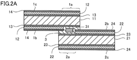
- FIG. 2A is a cross-sectional view of a portion where the first superconducting wire 1 and the second superconducting wire 2 are joined in the superconducting wire according to the first embodiment.
- the first superconducting wire 1 has a first superconducting layer 11, a first reinforcing layer 12, a first internal connection member 13, and a first surface connection member 14. is doing.
- the second superconducting wire 2 has a second superconducting layer 21, a second reinforcing layer 22, a second internal connection member 23, and a second surface connection member 24.
- the first superconducting wire 1 has a first end 1a.
- the second superconducting wire 2 has a second end 2a.
- the first end 1 a is a portion located at the end in the longitudinal direction of the first superconducting wire 1.
- the second end 2 a is a portion located at the end in the longitudinal direction of the second superconducting wire 2.
- the first superconducting wire 1 has a first surface 1b and a first back surface 1c.
- the first back surface 1c is a surface opposite to the first surface 1b.
- the second superconducting wire 2 has a second surface 2b and a second back surface 2c.
- the second back surface 2c is a surface opposite to the second surface 2b.
- the first superconducting layer 11 and the second superconducting layer 21 are layers containing, for example, a bismuth (Bi) high-temperature superconducting oxide in a silver (Ag) sheath.
- a bismuth (Bi) high-temperature superconducting oxide in a silver (Ag) sheath is not restricted to this.
- a nickel (Ni) alloy is used for the first reinforcing layer 12 and the second reinforcing layer 22.
- the material used for the first reinforcing layer 12 and the second reinforcing layer 22 is not limited to this.
- stainless steel, copper (Cu) alloy, or the like can be used as the first reinforcing layer 12 and the second reinforcing layer 22.
- the material used for the first reinforcing layer 12 may be the same material as the material used for the second reinforcing layer 22 or may be a different material.
- first internal connection member 13 and the second internal connection member 23 for example, lead-free solder such as tin (Sn) silver (Ag) alloy is used.
- the first internal connection member 13 and the second internal connection member 23 preferably have a melting point higher than that of the connection member 3.
- first surface connecting member 14 and the second surface connecting member 24 for example, lead-free solder such as tin (Sn) silver (Ag) alloy is used.
- the first surface connection member 14 and the second surface connection member 24 may be the same material as the first internal connection member 13 and the second internal connection member 23 or may be different materials. Good.
- the first surface connection member 14 and the second surface connection member 24 preferably have a melting point higher than that of the connection member 3.
- a first reinforcing layer 12 is provided on the first front surface 1b side and the first back surface 1c side of the first superconducting layer 11. On the first surface 1b side located at the first end 1a, all of the first reinforcing layer 12 is removed.
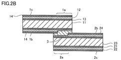
- FIG. 2B is a cross-sectional view of a portion where the first superconducting wire 1 and the second superconducting wire 2 are joined in the superconducting wire according to the first modification of the first embodiment. As shown in FIG. 2B, a part of the first reinforcing layer 12 may be removed on the first surface 1b side located at the first end 1a.
- the 1st surface 1b side of the 1st superconducting layer 11 located in the 1st edge part 1a is covered with the 1st reinforcement layer 12, the 1st surface located in the 1st edge part 1a
- the thickness of the first reinforcing layer 12 on the 1b side is thinner than the thickness of the first reinforcing layer 12 on the first surface 1b side, which is located other than the first end 1a.
- the 1st edge part 1a should just be a part from which at least one part of the 1st reinforcement layer 12 by the side of the 1st surface 1b was removed.
- a second reinforcing layer 22 is provided on the second surface 2b side and the second back surface 2c side of the second superconducting layer 21. On the second surface 2b side located at the second end 2a, the second reinforcing layer 22 is all removed.
- a part of the second reinforcing layer 22 may be removed on the second surface 2b side located at the second end 2a.
- the second surface 2b side of the second superconducting layer 21 located at the second end 2a is covered by the second reinforcing layer 22, but the second surface located at the second end 2a.
- the thickness of the second reinforcing layer 22 on the 2b side is thinner than the thickness of the second reinforcing layer 22 on the second surface 2b side, which is located other than the second end 2a.
- the 2nd edge part 2a should just be a part from which at least one part of the 2nd reinforcement layer 22 by the side of the 2nd surface 2b was removed.
- the first reinforcing layer 12 is provided on the first superconducting layer 11 in a state where tension is applied. As a result, the first reinforcing layer 12 causes a compressive strain to the first superconducting layer 11.
- the compressive strain generated in the first superconducting layer 11 positioned at the first end 1a may be smaller than the compressive strain generated in the first superconducting layer 11 positioned other than the first end 1a. Good.
- the compressive strain generated on the first surface 1b side of the first superconducting layer 11 located at the first end 1a is the first back surface 1c side of the first superconducting layer 11 located at the first end 1a.
- the width in the longitudinal direction of the first end portion 1a is preferably narrow. Specifically, in this case, the width in the longitudinal direction of the first end 1a is preferably 20 mm or less.
- the second reinforcing layer 22 is provided on the second superconducting layer 21 in a state where tension is applied. As a result, the second reinforcing layer 22 causes compressive strain with respect to the second superconducting layer 21. Even if the compressive strain generated in the second superconducting layer 21 positioned at the second end 2a is smaller than the compressive strain generated in the second superconducting layer 21 positioned other than the second end 2a. Good.
- the compressive strain generated on the second surface 2b side of the second superconducting layer 21 located at the second end 2a is caused by the second back surface 2c side of the second superconducting layer 21 located at the second end 2a. Is smaller than the compressive strain occurring in the second end portion 2a, the width in the longitudinal direction of the second end 2a is preferably narrow. Specifically, in this case, the width in the longitudinal direction of the second end 2a is preferably 20 mm or less.
- the compression strain is measured by X-ray or neutron diffraction. Further, the compression strain may be measured using a spring board.
- the first internal connection member 13 is provided between the first superconducting layer 11 and the first reinforcing layer 12. Thereby, the 1st superconducting layer 11 and the 1st reinforcement layer 12 are joined.
- the second internal connection member 23 is provided between the second superconducting layer 21 and the second reinforcing layer 22. Thereby, the 2nd superconducting layer 21 and the 2nd reinforcement layer 22 are joined.
- the 1st reinforcement layers 12 by the side of the 1st surface 1b located in the 1st edge part 1a are removed, the 1st by the side of the 1st surface 1b located in the 1st edge part 1a is 1st.
- the internal connection member 13 may be removed.
- the internal connection member 23 may be removed.
- the first surface connecting member 14 is provided on the first reinforcing layer 12 on the first surface 1b side and the first back surface 1c side.
- the second surface connecting member 24 is provided on the second reinforcing layer 22 on the second surface 2b side and the second back surface 2c side.
- the first surface 1b located at the first end 1a is joined to the second surface 2b located other than the second end 2a.
- the second surface connecting member on the second surface 2b side where the first inner connecting member 13 on the first surface 1b side located on the first end 1a is located on the other side than the second end 2a.
- the second surface 2b positioned at the second end 2a is joined to the first surface 1b positioned other than the first end 1a.
- the first surface connecting member on the first surface 1b side where the second inner connecting member 23 on the second surface 2b side located on the second end 2a is located on a side other than the first end 1a. 14.
- the first reinforcing layer 12 is provided on the first surface 1b side positioned at the first end 1a, and the second surface 2b side positioned on the second end 2a is the second side.
- the first reinforcing layer 12 on the first surface 1b side located at the first end 1a is on the second surface 2b side other than the second end 2a.
- the second reinforcing layer 22 on the second surface 2b side that is joined to the second surface connecting member 24 and located on the second end 2a is located on the first surface 1b side that is located on the side other than the first end 1a. It is joined to the first surface connecting member 14.
- a gap is provided between the end of the first reinforcing layer 12 on the first surface 1b side and the end of the second reinforcing layer on the second surface 2b side.
- the first internal connection member 13 on the first surface 1b side located on the first end 1a is the second on the second surface 2b side located on the second end 2a.
- the internal connection member 23 is joined.
- the first reinforcing layer 12 is provided on the first surface 1b side positioned at the first end 1a, and the second surface 2b side positioned on the second end 2a is the second side.
- the first reinforcing layer 12 on the first surface 1b side located at the first end 1a is on the second surface 2b side located on the second end 2a.
- the second reinforcing layer 22 is joined by the connecting member 3.
- a conductive member 31 may be provided in the connecting member 3 between the first surface 1b located at the first end 1a and the second surface 2b located at the second end 2a.
- a material having a higher electrical conductivity than that of the connection member 3 is used for the conductive member 31.
- the connecting member 3 is a solder such as an Sn alloy
- the conductive member 31 is made of Cu, Ag, gold (Au), or the like.
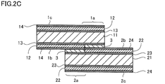
- FIG. 2C is a cross-sectional view at a portion where the first superconducting wire 1 and the second superconducting wire 2 are joined in the superconducting wire according to the second modification of the first embodiment.
- no gap may be provided between the end of the first reinforcing layer 12 on the first surface 1b side and the end of the second reinforcing layer on the second surface 2b side. . That is, the end of the first reinforcing layer 12 on the first surface 1b side and the end of the second reinforcing layer on the second surface 2b side may be in contact with each other.
- the 1st reinforcement layer 12 is provided in the 1st surface 1b side located in the 1st edge part 1a
- the 2nd reinforcement layer 22 is provided in the 2nd surface 2b side located in the 2nd edge part 2a.
- the end of the first reinforcing layer 12 on the first surface 1b side located outside the first end 1a is the second end on the second surface 2b side located outside the second end 2a. It may be in contact with the end of the reinforcing layer 22.
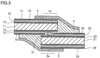
- FIG. 3 is a cross-sectional view of a third modification of the superconducting wire according to the first embodiment.
- the superconducting wire according to the first embodiment may have a first reinforcing member 4 and a second reinforcing member 5. Note that the superconducting wire according to the first embodiment may include only one of the first reinforcing member 4 and the second reinforcing member 5.
- the first reinforcing member 4 is provided on the first back surface 1 c of the first superconducting wire 1.
- the end of the first reinforcing member 4 protrudes from the first end 1 a and is joined to the second surface 2 b of the second superconducting wire 2 by the connecting member 3.
- the second reinforcing member 5 is provided on the second back surface 2 c of the second superconducting wire 2.
- the end of the second reinforcing member 5 protrudes from the second end 2 a and is joined to the first surface 1 b of the first superconducting wire 1 by the connecting member 3.
- the first reinforcing member 4 and the second reinforcing member 5 may be made of a material different from that of the first reinforcing layer 12 and the second reinforcing layer 22, or the same material may be used.
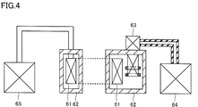
- FIG. 4 is a schematic diagram of the superconducting device 6 using the superconducting wire according to the first embodiment.
- the superconducting device 6 using the superconducting wire according to the first embodiment is, for example, a refrigerator-cooled superconducting magnet system.
- the apparatus using the superconducting wire which concerns on 1st Embodiment is not restricted to this.
- the superconducting device 6 using the superconducting wire according to the first embodiment has a superconducting coil body 61, for example.
- the superconducting wire according to the first embodiment is used for the superconducting coil body 61.
- the superconducting device 6 using the superconducting wire according to the first embodiment has, as other configurations, for example, a heat insulating container 62 for storing the superconducting coil body 61 and a refrigerator 63 for cooling the superconducting coil body 61. And a compressor 64 for driving the refrigerator 63, and a power source 65.
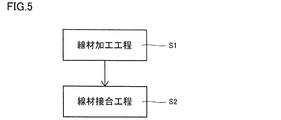
- FIG. 5 is a process diagram of the method of manufacturing a superconducting wire according to the first embodiment.
- the manufacturing method of the superconducting wire according to the first embodiment includes a wire rod processing step S1 and a wire rod bonding step S2.
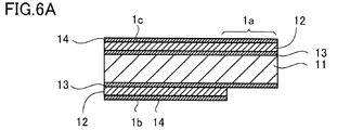
- FIG. 6A is a cross-sectional view of the first superconducting wire 1 after the wire processing step S1 is performed.
- FIG. 6B is a cross-sectional view of the second superconducting wire 2 after the wire processing step S1 is performed.
- the first reinforcing layer 12 on the first surface 1 b side located at the first end 1 a and the second surface located at the second end 2 a by the wire processing step S ⁇ b> 1. All of the second reinforcing layer 22 on the 2b side is removed.
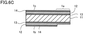
- FIG. 6C is a cross-sectional view of a modified example of the first superconducting wire 1 after the wire processing step S1 is performed.
- 6D is a cross-sectional view of a modified example of the second superconducting wire 2 after the wire processing step S1 is performed. As shown in FIG. 6C and FIG. 6D, the first reinforcing layer 12 on the first surface 1b side located at the first end 1a and the second surface located at the second end 2a by the wire rod processing step S1. A part of the second reinforcing layer 22 on the 2b side may be removed.
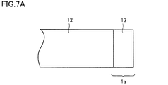
- FIG. 7A is a top view seen from the first surface 1b side of the first superconducting wire 1 after the wire processing step S1 is performed.
- the first reinforcing layer 12 on the first surface 1b side located at the first end 1a is such that the end of the first reinforcing layer 12 is perpendicular to the longitudinal direction of the first superconducting wire 1. May be removed.
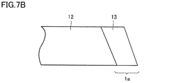
- FIG. 7B is a top view of the modified example of the first superconducting wire 1 after the wire processing step S1 is viewed from the first surface 1b side. As shown in FIG.
- FIG. 7B is a top view as seen from the first surface 1b side of another modified example of the first superconducting wire 1 after the wire processing step S1 is performed. As shown in FIG. 7C, when the end of the first superconducting wire 1 is removed so as to be inclined in the longitudinal direction of the first superconducting wire 1, the tip portion may be further removed.
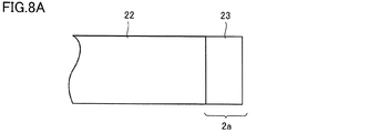
- FIG. 8A is a top view of the second superconducting wire 2 as viewed from the second surface 2b side after the wire material processing step S1 is performed.
- the second reinforcing layer 22 on the second surface 2b side located at the second end 2a is such that the end of the second reinforcing layer 22 is perpendicular to the longitudinal direction of the second superconducting wire 2. May be removed.
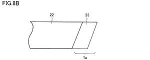
- FIG. 8B is a top view seen from the second surface 2b side of the modified example of the second superconducting wire 2 after the wire processing step S1 is performed. As shown in FIG.
- the second reinforcing layer 22 on the second surface 2b side located at the second end 2a has the end of the second reinforcing layer 22 in the longitudinal direction of the second superconducting wire 2.
- the end of the second superconducting wire 2 may be removed so as to be inclined with respect to the longitudinal direction of the second superconducting wire 2.
- the end of the second reinforcing layer 22 and the end of the second superconducting wire 2 are overlapped so that the first surface 1b and the second surface 2b face each other. It is preferably removed so as to be parallel to the end and the end of the first superconducting wire 1.
- FIG. 8C is a top view as seen from the second surface 2b side of another modification of the second superconducting wire 2 after the wire processing step S1 is performed. As shown in FIG. 8C, when the end of the second superconducting wire 2 is removed so as to be inclined in the longitudinal direction of the second superconducting wire 2, the tip portion may be further removed. By having such a shape, the stress concentration generated between the first superconducting wire 1 and the second superconducting wire 2 can be further relaxed.
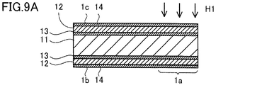
- FIG. 9A is a cross-sectional view when heating the first end 1a of the first superconducting wire 1 in the wire processing step S1.
- heat H1 is applied to the first end 1a of the first superconducting wire 1.
- the first internal connection member 13 located at the first end 1a is melted.
- the 1st reinforcement layer 12 is with respect to the 1st superconducting layer 11 located in the 1st edge part 1a. The compression strain that has been applied is released.
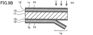
- FIG. 9B is a cross-sectional view when the first reinforcing layer 12 of the first superconducting wire 1 is peeled off in the wire material processing step S1.
- the first reinforcing layer 12 on the first surface 1b side is peeled off.
- the first reinforcing layer 12 on the first surface 1b side is peeled off in a state where the first internal connection member 13 located at the first end 1a is melted (that is, in a state where the heat H1 is applied). Is called.
- the portion where the first reinforcing layer 12 on the first surface 1b side is peeled off is removed by cutting or the like.
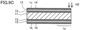
- FIG. 9C is a cross-sectional view when heating the first end 1a of the first superconducting wire 1 in the modification of the wire processing step S1.
- FIG. 9D is a cross-sectional view when the first reinforcing layer 12 of the first superconducting wire 1 is peeled off in a modification of the wire processing step S1.
- the first reinforcing layer 12 on the first surface 1b side is peeled off. May be. In this case, only the first internal connection member 13 located at the end on the first end 1a side is melted by the heat H2.
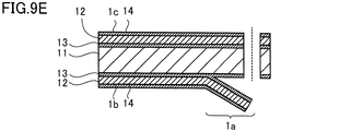
- FIG. 9E is a cross-sectional view when cutting a part of the first end 1a of the first superconducting wire 1 in the wire processing step S1.
- the part containing the 1st internal connection member 13 fuse
- the first reinforcing layer 12 on the first surface 1b side located at the first end 1a and a part of the second reinforcing layer 22 on the second surface 2b side located in the second end 2a are removed.
- the first reinforcing layer 12 on the first surface 1b side located on the first end 1a and the second reinforcing layer 22 on the second surface 2b side located on the second end 2a Polishing is performed.
- the second superconducting wire 2 is subjected to the same processing as that for the first superconducting wire 1, whereby the second reinforcing layer 22 on the second surface 2 b side located at the second end 2 a. All or a part of is removed.
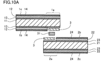
- FIG. 10A is a cross-sectional view of the superconducting wire according to the first embodiment before joining in the wire joining step S2.
- the first superconducting wire 1 and the second superconducting wire 2 are composed of a first surface 1b and a second end 2a located at the first end 1a.
- the second surface 2b located outside is opposed to the second surface 2b, and the second surface 2b located at the second end 2a is opposed to the first surface 1b located outside the first end 1a.
- FIG. 11A is a cross-sectional view of a superconducting wire according to a third modification of the first embodiment before joining in the wire joining step S2.
- the 1st reinforcement member 4 when the 1st reinforcement member 4 is provided, the 1st reinforcement member 4 is further arrange
- the second reinforcing member 5 when the second reinforcing member 5 is provided, the second reinforcing member 5 is further disposed on the second back surface 2c and the first front surface 1b side.
- the first end 1a is positioned between the first surface 1b positioned at the first end 1a and the second surface 2b positioned other than the second end.
- the connection member 3 is supplied.
- a conductive member 31 may be inserted between the connection members 3 between the first surface 1b located at the first end 1a and the second surface 2b located at the second end 2a.
- the connection member 3 is supplied with forms, such as a paste form and a sheet form, for example.
- flux may be applied to the first surface 1b of the first superconducting wire 1, the second surface 2b of the second superconducting wire 2, the surface of the connecting member 3, and the surface of the conductive member 31. Good.
- connection member 3 is also supplied between the reinforcing member 5 and the first surface 1b and the second back surface 2c.
- the first back surface 1c of the first superconducting wire 1, the second back surface 2c of the second superconducting wire 2, and the surface facing the second surface 2b of the first reinforcing member 4 The flux may also be applied to the surface of the second reinforcing member 5 that faces the first surface 1 b and the surface of the connecting member 3.
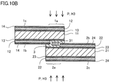
- FIG. 10B is a cross-sectional view of the superconducting wire according to the first embodiment at the time of joining in the wire joining step S2.
- the first superconducting wire 1 and the second superconducting wire 2 are joined. More specifically, the pressure P is applied to the portion where the first superconducting wire 1 and the second superconducting wire 2 overlap.
- the pressure P is preferably kept constant from the start of application of heat H3 (described later) to the end of cooling. Thereafter, heat H3 is applied to the first superconducting wire 1 and the second superconducting wire 2.
- the heating time for applying the heat H3 is preferably 10 seconds or longer. After the heating time is over, cooling is performed using, for example, a cooling fan. For safety reasons, the cooling is preferably performed until the temperature is 50 ° C. or lower. Thereby, joining with the 1st superconducting wire 1 and the 2nd superconducting wire 2 is performed.
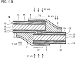
- FIG. 11B is a cross-sectional view of the superconducting wire according to the third modification of the first embodiment at the time of joining in the wire joining step S2.
- the 1st reinforcement member 4 and the 2nd reinforcement member 5 are provided, as shown to FIG. 11B, the part with which the 1st reinforcement member 4 and the 2nd reinforcement layer 22 by the side of the 2nd surface 2b overlap
- the pressure P is applied to the part which the 2nd reinforcement member 5 and the 1st reinforcement layer 12 by the side of the 1st surface 1b overlap.
- the pressure P is preferably kept constant from the start of application of heat H3 (described later) to the end of cooling. Thereafter, heat H3 is applied to the first superconducting wire 1 and the second superconducting wire 2.
- the heating time for applying the heat H3 is preferably 10 seconds or longer. After the heating time is over, cooling is performed using, for example, a cooling fan. For safety reasons, the cooling is preferably performed until the temperature is 50 ° C. or lower. Thereby, the connection member 3 is melted, the first reinforcing member 4 and the second reinforcing layer 22 on the second surface 2b side are joined, and the first reinforcing member 5 and the first surface 1b side are connected. The reinforcing layer 12 is joined.
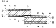
- FIG. 12 is a cross-sectional view of the superconducting wire according to the first comparative example.
- the superconducting wire according to the first comparative example has a first superconducting wire 1, a second superconducting wire 2, and a connecting member 3.
- the structures of the first superconducting wire 1 and the second superconducting wire 2 of the superconducting wire according to the first comparative example are the same as those of the superconducting wire according to the first embodiment.
- the first superconducting wire 1 and the second superconducting wire 2 have the first surface 1b of the first superconducting layer 11 located at the first end 1a. It is joined by the connecting member 3 so that the side faces the second surface 2b side of the second superconducting layer 21 located at the second end 2a.
- the first surface 1b side of the first superconducting layer 11 located at the first end 1a is the second superconducting layer 21 located at the second end 2a.
- the end of the portion where the 2 surface 2b side is joined becomes a stress concentration location.
- the first superconducting wire 1 and the second superconducting wire 2 of the superconducting wire according to the first embodiment and the superconducting wire according to the first comparative example used in the bending test and the tensile test have a width of 4.5 mm.
- the thickness is 0.31 mm
- the first internal connection member 13 and the second internal connection member 23 are Pb-free solder
- the connection member 3 is PbSn eutectic solder
- the first reinforcement layer 12 and the second reinforcement layer 22 Is a Ni alloy
- the overlapping length (wrap length) of the first superconducting wire 1 and the second superconducting wire 2 is 20 mm.
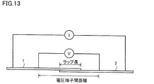
- FIG. 13 is a schematic diagram of critical current measurement.
- the critical current measurement is performed by a four-terminal method with a voltage terminal distance of 220 mm centering on a portion where the first superconducting wire 1 and the second superconducting wire 2 are joined in liquid nitrogen. This is performed by acquiring a voltage curve and reading a current value based on an electric field reference of 1 ⁇ V / cm in a curve calculated so as to exclude a resistance component found by Ohm's law from the acquired curve.
- the critical current is measured in a state after performing both bendings on the superconducting wire according to the first embodiment and the superconducting wire according to the first comparative example, and the critical current in the state after performing both bendings.
- the two bendings were performed by bending the first superconducting wire 1 along a jig having a predetermined diameter and then bending the second superconducting wire 2 along the jig at room temperature. . If the critical current is measured after both bends and exceeds 95% of the critical current measured prior to the bending test, double bending and critical current measurement are performed again using a jig with a smaller diameter. Was repeated.
- the allowable bending diameter of the superconducting wire according to the first comparative example was 180 mm (the first superconducting wire 1 and the second superconducting wire 2). (4.5 times that of a single case).
- the allowable bending diameter of the superconducting wire according to the first embodiment was 80 mm (the first superconducting wire 1 and the second superconducting wire.
- the superconducting wire according to the first embodiment exhibited a bending characteristic that was 2.25 times better than the superconducting wire according to the first comparative example.
- the allowable bending diameter when the conductive member 31 was provided was 90 mm.
- the tensile test is performed in liquid nitrogen.
- the critical current is measured in a state where a predetermined tensile tension is applied to the superconducting wire according to the first embodiment and the superconducting wire according to the first comparative example, and the critical current in the state where the tensile tension is applied is determined prior to the tensile test. This was done by measuring the tensile tension when it was below 95% of the measured critical current.
- the allowable tensile strength is calculated by tensile tension / wire width / wire thickness (when the first reinforcing layer 12 and the second reinforcing layer 22 are made of the same material, the wire width and wire thickness include the first The average values of the wire width and the wire thickness of the superconducting wire 1 and the second superconducting wire 2 are used. If the first reinforcing layer 12 and the second reinforcing layer are different materials, the wire width and the wire thickness are used. For the first superconducting wire 1 and the second superconducting wire 2, the wire width and wire thickness of the superconducting wire having a low tensile strength are used.
- the allowable tensile stress was 424 MPa.
- the allowable tensile strength of the superconducting wire according to the first comparative example was 165 MPa (first superconducting wire 1 and second superconducting wire 2. 39% of the case alone.
- the allowable tensile strength of the superconducting wire according to the first embodiment was 389 MPa (first superconducting wire 1, second superconducting wire). 91% of the case of wire 2 alone). That is, the superconducting wire according to the first embodiment exhibited 2.33 times better tensile properties than the superconducting wire according to the first comparative example.
- the allowable tensile strength when the conductive member 31 was provided in the superconducting wire according to the first embodiment was 389 MPa.
- the superconducting wire according to the first comparative example has a stress concentration portion and the reinforcing layer is interrupted in the longitudinal direction.
- the superconducting wire according to the first embodiment of the first embodiment does not have a significant stress concentration location, and the first reinforcing layer 12 and the second reinforcing layer 22 are joined without interruption in the longitudinal direction. Has been. Therefore, as shown in the bending test result, the superconducting wire according to the first embodiment can obtain good mechanical characteristics against bending deformation, tensile deformation, and the like.
- the first reinforcing layer 12 is not provided on the first surface 1b side located at the first end 1a (or other than the first end 1a).
- the second reinforcing layer 22 is not provided on the second surface 2b side located at the second end portion 2a (thinner layer is thinner than the first reinforcing layer 12 on the first surface 1b side located at the second side). (Alternatively, it is thinner than the second reinforcing layer 22 on the second surface 2b side located outside the second end portion 2a), so that the first reinforcing layer 12 and the second reinforcing layer 22 are the first.
- the increase in connection resistance due to the positioning between the superconducting layer 11 and the second superconducting layer 21 is suppressed. This point will be described below.
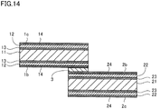
- FIG. 14 is a cross-sectional view of a superconducting wire according to the second comparative example.
- the superconducting wire according to the second comparative example has a first superconducting wire 1, a second superconducting wire 2, and a connecting member 3.
- the first superconducting wire 1 and the second superconducting wire 2 are connected so that the first surface 1b located at the first end 1a and the second surface 2b located at the second end 2a face each other.
- the first superconducting wire 1 in the superconducting wire according to the second comparative example is positioned other than the first reinforcing layer 12 on the first surface 1b side located at the first end 1a and the first end 1a. It differs from the superconducting wire according to the first embodiment in that the first reinforcing layer 12 on the first surface 1b side has the same thickness.
- the second superconducting wire 2 in the superconducting wire according to the second comparative example is other than the second reinforcing layer 22 on the second surface 2b side located at the second end 2a and the second end 2a. This is different from the superconducting wire according to the first embodiment in that the second reinforcing layer 22 on the second surface 2b side located at the same thickness has the same thickness.
- the first superconducting wire 1 and the second superconducting wire 2 of the superconducting wire according to the first embodiment and the superconducting wire according to the second comparative example have a width of 4.5 mm, a thickness of 0.31 mm, and a first
- the internal connection member 13 and the second internal connection member 23 are Pb-free solder
- the connection member 3 is PbSn eutectic solder
- the first reinforcing layer 12 and the second reinforcing layer 22 are Ni alloy
- the overlapping length (wrap length) of the second superconducting wire 2 is 20 mm.
- a current-voltage curve is obtained by the four-terminal method with a distance between the voltage terminals of 220 mm centering on the portion where the first superconducting wire 1 and the second superconducting wire 2 are joined in liquid nitrogen.
- the slope of the resistance component found by Ohm's law is calculated from the obtained curve.
- connection resistance of the superconducting wire according to the second comparative example was 696 n ⁇ .
- connection resistance of the superconducting wire according to the first embodiment was 109 n ⁇ .
- the superconducting wire according to the first embodiment exhibited a connection resistance 6.39 times better than the superconducting wire according to the first comparative example.
- the connection resistance was 73 n ⁇ .
- the allowable bending diameter was 150 mm and the allowable tensile strength was 424 MPa.
- the first reinforcing layer 12 on the first surface 1b side located at the first end 1a is not provided (or the first end).
- a second reinforcing layer 22 on the second surface 2b side located on the second end 2a is provided, which is thinner than the first reinforcing layer 12 on the first surface 1b side located outside the portion 1a). (Or thinner than the second reinforcing layer 22 on the second surface 2b side other than the second end 2a).
- the first reinforcing layer 12 on the side of the first surface 1b located other than the first end 1a and the first end 1a has an equal thickness.
- the second reinforcing layer 22 on the second surface 2b side, which is located other than the second end 2a and the second end 2a has an equal thickness.
- the superconducting wire according to the first embodiment is disposed between the first superconducting layer 11 and the second superconducting layer 21 as compared with the superconducting wire according to the second comparative example.
- the thicknesses of the first reinforcing layer 12 and the second reinforcing layer 22 having a relatively high electrical resistance value are reduced. Therefore, in the superconducting wire according to the first embodiment, an increase in connection resistance is suppressed.
- the first reinforcing layer 12 on the first surface 1b side located at the first end 1a is all removed, and the second located at the second end 2a.
- the first electric resistance value that is relatively high between the first superconducting layer 11 and the second superconducting layer 21 is disposed.
- the thickness of the reinforcement layer 12 and the 2nd reinforcement layer 22 is thinner. Therefore, in this case, the connection resistance value can be further reduced.
- the electric resistance value of the conductive member 31 is lower than that of the connecting member 3.
- the connection resistance with the second superconducting layer 21 can be further reduced.
- the superconducting wire according to the first embodiment includes the first reinforcing member 4 and the second reinforcing member 5
- the first reinforcing member 4 and the second reinforcing member 5 are the first by the connecting member 3.
- the superconducting wire 1 and the second superconducting wire 2 are reinforced. Therefore, in this case, it is possible to obtain better mechanical characteristics against bending deformation, tensile deformation, and the like.
- the first superconducting layer 11 has a compressive strain caused by the first reinforcing layer 12, and the second superconducting layer 21 is caused by the second reinforcing layer 22.
- compressive strain When compressive strain is generated, the tensile stress generated in the first superconducting layer 11 and the second superconducting layer 21 when bending deformation, tensile deformation, or the like is applied is relaxed. Therefore, in this case, it is possible to obtain better mechanical characteristics against bending deformation, tensile deformation, and the like.
- the compressive strain with respect to the first superconducting layer 11 located at the first end 1a is more than the compressive strain with respect to the first superconducting layer located other than the first end 1a. If the compressive strain on the second superconducting layer 21 located at the second end 2a is smaller than the compressive strain on the second superconducting layer 21 located outside the second end 2a, The first reinforcing layer 12 on the first surface 1b side located at the first end 1a and the second reinforcing layer 22 on the second surface 2b side located in the second end 2a are removed when the first reinforcing layer 12 is removed. The warp of the end 1a and the second end 2a is small. Therefore, in this case, the width of the first end portion 1a and the second end portion 2a can be widened. As a result, the connection resistance between the first superconducting wire 1 and the second superconducting wire 2 is reduced. Further reduction is possible.
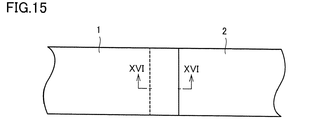
- FIG. 15 is a top view of the superconducting wire according to the second embodiment.
- the superconducting wire according to the second embodiment is the same as the superconducting wire according to the first embodiment, the first superconducting wire 1, the second superconducting wire 2, and the connecting member 3 ( 16A).
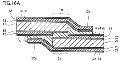
- FIG. 16A is a cross-sectional view of a portion where the first superconducting wire 1 and the second superconducting wire 2 are joined in the superconducting wire according to the second embodiment.
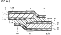
- FIG. 16B is a cross-sectional view of a portion where the first superconducting wire 1 and the second superconducting wire 2 are joined in a superconducting wire according to a modification of the second embodiment. 16A and 16B, the shape of the first reinforcing layer 12 on the first back surface 1c side of the first superconducting wire 1 and the second reinforcing layer 22 on the second back surface 2c side of the second superconducting wire 2 are shown. Is different from the superconducting wire according to the first embodiment.
- the first reinforcing layer 12 on the first back surface 1c side has a first protruding portion 12a protruding from the first end portion 1a.
- the first protrusion 12a is joined to the second reinforcing layer 22 on the second surface 2b side by the connecting member 3.
- the second reinforcing layer 22 on the second back surface 2c side has a second protruding portion 22a protruding from the second end 2a.
- the second protrusion 22a is joined to the first reinforcing layer 12 on the first surface 1b side by the connecting member 3.
- the 1st surface 1b located in the 1st edge part 1a is arrange
- the first internal connection member 13 on the first surface 1b located at the first end 1a is on the second surface 2b located at the second end 2a.
- the second internal connection member 23 is joined.
- the 1st reinforcement layer 12 is provided in the 1st surface 1b side of the 1st superconducting layer 11 located in the 1st edge part 1a, and it is located in the 2nd edge part 2a.
- the first reinforcing layer 12 on the first surface 1b side located in the first end 1a is The connecting member 3 is joined to the second reinforcing layer 22 on the second surface 2b side located at the second end 2a.
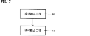
- FIG. 17 is a process diagram of the method of manufacturing a superconducting wire according to the second embodiment.
- the superconducting wire manufacturing method according to the second embodiment includes a wire rod processing step S1 and a wire rod bonding step S2, as shown in FIG. is doing.
- the wire joining step S2 of the superconducting wire manufacturing method according to the second embodiment is different from the wire joining step S2 of the superconducting wire manufacturing method according to the first embodiment.
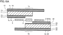
- FIG. 18A is a cross-sectional view of the superconducting wire according to the second embodiment before joining in the wire joining step S2.
- the first superconducting wire 1 and the second superconducting wire 2 are formed on the first surface 1b and the second end 2a located at the first end 1a.
- the 2nd surface 2b located is arrange
- the first protrusion 12a is arranged to face the second surface 2b
- the second protrusion 22a is arranged to face the first surface 1b.
- connection member 3 is supplied between the second protrusion 22a and the first surface 1b.
- the first surface 1b of the first superconducting wire 1, the second surface 2b of the second superconducting wire 2, the surface of the first projecting portion 12a facing the second surface 2b, the second surface A flux may be applied to the surface of the protrusion 22 a facing the first surface 1 b and the surface of the connecting member 3.
- FIG. 18B is a cross-sectional view of the superconducting wire according to the second embodiment at the time of joining in the wire joining step S2. Thereafter, as shown in FIG. 18B, the first superconducting wire 1 and the second superconducting wire 2 are joined. More specifically, heat H3 and pressure P are applied to the portion where the first superconducting wire 1 and the second superconducting wire 2 overlap. Thereby, the connection member 3 is melted, and the first superconducting wire 1 and the second superconducting wire 2 are joined.
- the superconducting wire according to the second embodiment is similar to the superconducting wire according to the first comparative example, and the first surface 1b located at the first end 1a and the second end 2a located at the second end 2a. There is a stress concentration point at the end of the joint with the two surfaces 2b.
- the first reinforcing layer 12 on the first back surface 1c side protrudes from the first end portion 1a and forms the second reinforcing layer 22 on the second surface 2b side. It is joined.
- the second reinforcing layer 22 on the second back surface 2c side protrudes from the second end 2a and is formed on the first reinforcing layer 12 on the first surface 1b side. It is joined.
- the joint between the first surface 1b located at the first end 1a and the second surface 2b located at the second end 2a is the first reinforcing layer 12 on the first back surface 1c side, the second Reinforced by the second reinforcing layer 22 on the back surface 2c side.
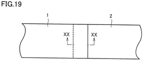
- FIG. 19 is a top view of a superconducting wire according to the third embodiment. As shown in FIG. 19, the superconducting wire according to the third embodiment is similar to the superconducting wire according to the first embodiment, in which the first superconducting wire 1, the second superconducting wire 2, and the connecting member 3 ( 20A)).
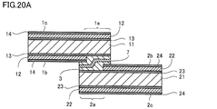
- FIG. 20A is a cross-sectional view of a portion where the first superconducting wire 1 and the second superconducting wire 2 are joined in the superconducting wire according to the third embodiment.
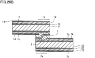
- FIG. 20B is a cross-sectional view of a portion where the first superconducting wire 1 and the second superconducting wire 2 are joined in the superconducting wire according to the first modification of the third embodiment.
- the superconducting wire according to the third embodiment is different from the superconducting wire according to the first embodiment in that it has a third reinforcing member 7.
- the first superconducting wire 1 and the second superconducting wire 2 are the first surface located at the first end 1a. 1b and the second surface 2b located outside the second end 2a face each other, and the second surface 2b located at the second end 2a and the first surface 1b other than the first end 1a It arrange
- the first reinforcing layer 12 on the first surface 1b side located at the first end 1a and the second surface 2b side located on the second end 2a are arranged.
- the first inner connecting member 13 on the first surface 1b side located at the first end 1a is located at the second surface other than the second end 2a.
- the second internal connection member 23 on the second surface 2b side that faces the second surface connection member 24 on the 2b side and is located at the second end 2a is located at a position other than the first end 1a. It faces the first surface connecting member 14 on the one surface 1b side.
- the first reinforcing layer 12 is provided on the first surface 1b side positioned at the first end 1a, and the second surface 2b side positioned on the second end 2a is second.
- the first reinforcing layer 12 on the first surface 1b side located at the first end 1a is on the second surface 2b side other than the second end 2a.
- the second reinforcing layer 22 facing the second surface connecting member 24 and located on the second end 2a on the second surface 2b side is located on the first surface 1b other than the first end 1a. It faces the first surface connecting member 14 on the side.
- the third reinforcing member 7 is provided between the first surface 1b and the second surface 2b in at least a part of the portion where the first superconducting wire 1 and the second superconducting wire 2 overlap. .
- the third reinforcing member 7 is provided between the first surface 1b and the second surface 2b over the entire length where the first superconducting wire 1 and the second superconducting wire 2 overlap. preferable.
- the third reinforcing member 7 has a first end between the first surface 1b located at the first end 1a and the second surface 2b located other than the second end 2a. Between the first surface 1b located at the part 1a and the second surface 2b located at the second end 2a, and between the first surface 1b and the second end 2a located other than the first end 1a It is provided between the second surface 2b.
- FIG. 21A is a cross-sectional view of a portion where a first superconducting member and a second superconducting member are joined in a superconducting wire according to a second modification of the third embodiment.
- FIG. 21B is a cross-sectional view of a portion where a first superconducting member and a second superconducting member are joined in a superconducting wire according to a third modification of the third embodiment.
- the third reinforcing member 7 may be composed of a plurality of members.
- the third reinforcing member 7 is joined to the first surface 1 b of the first superconducting wire 1 and the second surface 2 b of the second superconducting wire 2 using the connecting member 3.
- the third reinforcing member 7 preferably has a lower electrical resistance value than the connecting member 3.
- the third reinforcing member 7 is preferably stronger than the connecting member 3.
- the material used for the third reinforcing member is, for example, a Cu alloy.
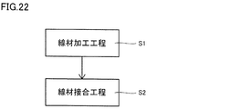
- FIG. 22 is a process diagram of the method of manufacturing a superconducting wire according to the third embodiment.
- the method of manufacturing a superconducting wire according to the third embodiment includes a wire rod processing step S1 and a wire rod bonding step S2.
- the wire processing step S1 in the method of manufacturing a superconducting wire according to the third embodiment is the same as that in the first embodiment.
- FIG. 23A is a cross-sectional view of the superconducting wire according to the third embodiment before joining in the wire joining step S2.
- the first superconducting wire 1 and the second superconducting wire 2 are other than the first surface 1b and the second end 2a located at the first end 1a.
- the second surface 2b located at the second end 2a is opposed, and the second surface 2b located at the second end 2a is opposed to the first surface 1b located other than the first end 1a. .
- the third reinforcing member 7 is inserted between the first surface 1b and the second surface 2b in at least a part of the portion where the first superconducting wire 1 and the second superconducting wire 2 overlap. Is done. Further, the connecting member 3 is supplied between the third reinforcing member 7 and the first surface 1b and between the third reinforcing member 7 and the second surface 2b. Prior to joining, flux is applied to the first surface 1b of the first superconducting wire 1, the second surface 2b of the second superconducting wire 2, the surface of the third reinforcing member 7, and the surface of the connecting member 3. May be.
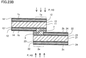
- FIG. 23B is a cross-sectional view of the superconducting wire according to the third embodiment at the time of joining in the wire joining step S2.
- the first superconducting wire 1 and the third reinforcing member 7 are joined and the second superconducting wire 2 and the third reinforcing member 7 are joined.
- heat H3 and pressure P are applied to the portion where the first superconducting wire 1 and the second superconducting wire 2 overlap.
- the connecting member 3 is melted, and the first superconducting wire 1 and the third reinforcing member 7 are joined and the second superconducting wire 2 and the third reinforcing member 7 are joined.
- the superconducting wire according to the third embodiment includes the third reinforcing member 7, and the third reinforcing member 7 has higher strength and lower electrical resistance than the connection member 3. Therefore, the superconducting wire according to the third embodiment has a lower connection resistance and a higher bending deformation than the case where the first superconducting wire 1 and the second superconducting wire 2 are directly joined by the connecting member 3. It is possible to obtain mechanical strength against tensile deformation and the like.
- SYMBOLS 1 1st superconducting wire, 1a 1st edge part, 1b 1st surface, 1c 1st back surface, 11 1st superconducting layer, 12 1st reinforcement layer, 12a 1st protrusion part, 13 1st inside Connecting member, 14 first surface connecting member, 2nd superconducting wire, 2a second end, 2b second surface, 2c second back surface, 21 second superconducting layer, 22 second reinforcing layer, 22a 2nd protrusion part, 23 2nd internal connection member, 24 2nd surface connection member, 3 connection member, 31 conductive member, 4 1st reinforcement member, 5 2nd reinforcement member, 6 superconducting equipment, 61 superconductivity Coil body, 62 insulation container, 63 refrigerator, 64 compressor, 65 power supply, 7 third reinforcing member, H1, H2, H3 heat, P pressure, S1 wire processing step, S2 wire joining step.
Landscapes
- Physics & Mathematics (AREA)
- Condensed Matter Physics & Semiconductors (AREA)
- General Physics & Mathematics (AREA)
- Engineering & Computer Science (AREA)
- Power Engineering (AREA)
- Manufacturing & Machinery (AREA)
- Superconductors And Manufacturing Methods Therefor (AREA)
- Manufacturing Of Electrical Connectors (AREA)
Abstract
第1表面と、第1表面の反対側の面である第1裏面とを有し、かつ第1の超電導層と、第1の補強層とを有する第1の超電導線材と、第2表面と、第2表面の反対側の面である第2裏面とを有し、かつ第2の超電導層と、第2の補強層とを有する第2の超電導線材と、第1の超電導線材と第2の超電導線材とを接合する接続部材とを備えている。第1の超電導線材は第1表面側の第1の補強層の少なくとも一部が除去されている第1の端部を有し、第2の超電導線材は第2表面側の第2の補強層の少なくとも一部が除去されている第2の端部を有している。第1の端部に位置する第1表面は、接続部材により、第2の端部以外に位置する第2表面に接合され、第2の端部に位置する第2表面は、接続部材により、第1の端部以外に位置する第1表面に接合されている。
Description
本発明は、超電導線及びその製造方法に関する。
本出願は、2016年3月11日出願の日本出願第2016-48786号に基づく優先権を主張し、前記日本出願に記載された全ての記載内容を援用するものである。
本出願は、2016年3月11日出願の日本出願第2016-48786号に基づく優先権を主張し、前記日本出願に記載された全ての記載内容を援用するものである。
超電導機器用の超電導線を作製するためには、長尺の超電導線材が必要とされる。通常、複数の超電導線材を順次接続していくことにより、超電導線材の長尺化が図られる。
複数の超電導線材を接続する構造として、特開2011-238513号公報(特許文献1)記載の接続構造が提案されている。特許文献1記載の第1の超電導線材は、超電導層と、内部はんだ層と、補強層とを有する。また、特許文献1記載の超電導線材は、端末部を有している。特許文献1記載の第2の超電導線材は、第1の超電導線材と同様の構造を有している。
超電導層は、第1面と、第2面とを有している。補強層は、第1面及び第2面上に設けられている。但し、第1面の端末部側に位置する領域上においては、補強層が設けられていない。すなわち、第1面の端末部側に位置する領域においては、超電導層が露出している。内部はんだ層は、補強層と第1面及び第2面との間に設けられており、補強層と超電導層とを接合している。
特許文献1記載の超電導線材の接続構造は、第1の超電導線材と、第2の超電導部材と、接続はんだ層とを有している。第1の超電導部材の第1面の端末部側に位置する領域において露出している超電導層が、第2の超電導部材の第1面の端末部側に位置する領域において露出している超電導層と対向するように配置されている。第1の超電導部材の第1面の端末部側に位置する領域において露出している超電導層と第2の超電導部材の第1面の端末部側に位置する領域において露出している超電導層とは、接続はんだにより接合されている。
本開示の超電導線は、第1表面と、第1表面の反対側の面である第1裏面とを有する第1の超電導線材と、第2表面と、第2表面の反対側の面である第2裏面とを有する第2の超電導線材と、第1の超電導線材と第2の超電導線材とを接合する接続部材とを備えている。第1の超電導線材は、第1の超電導層と、第1の超電導層の第1表面側及び第1裏面側に設けられた第1の補強層とを有する。第2の超電導線材は、かつ第2の超電導層と、第2の超電導層の第2表面側及び第2裏面側に設けられた第2の補強層とを有する。
第1の超電導線材は、第1表面側の第1の補強層の少なくとも一部が除去されている第1の端部を有している。第2の超電導線材は、第2表面側の第2の補強層の少なくとも一部が除去されている第2の端部を有している。
第1の端部に位置する第1表面は、接続部材により、第2の端部以外に位置する第2表面に接合され、第2の端部に位置する第2表面は、接続部材により、第1の端部以外に位置する第1表面に接合されている。
[本開示が解決しようとする課題]
特許文献1記載の超電導線材の接合構造は、曲げ変形、引張変形等を受けた際の機械的特性が十分ではない場合がある。すなわち、特許文献1記載の超電導線材の接合構造においては、曲げ変形、引張変形等を受けた場合に、超電導層が接続はんだを介して互いに対向している部分の端に、応力集中が生じやすい。
特許文献1記載の超電導線材の接合構造は、曲げ変形、引張変形等を受けた際の機械的特性が十分ではない場合がある。すなわち、特許文献1記載の超電導線材の接合構造においては、曲げ変形、引張変形等を受けた場合に、超電導層が接続はんだを介して互いに対向している部分の端に、応力集中が生じやすい。
本開示は、このような従来技術の問題点に鑑みてなされたものである。すなわち、本開示は、機械的特性に優れた超電導線を提供するものである。
[本開示の効果]
本開示によれば、曲げ変形、引張変形等に対する良好な機械的特性を得ることが可能となる。
本開示によれば、曲げ変形、引張変形等に対する良好な機械的特性を得ることが可能となる。
[本発明の実施形態の説明]
最初に本発明の実施態様を列記して説明する。
最初に本発明の実施態様を列記して説明する。
(1)本発明の一実施態様に係る超電導線は、第1表面と、第1表面の反対側の面である第1裏面とを有する第1の超電導線材と、第2表面と、第2表面の反対側の面である第2裏面とを有する第2の超電導線材と、第1の超電導線材と第2の超電導線材とを接合する接続部材とを備えている。第1の超電導線材は、第1の超電導層と、第1の超電導層の第1表面側及び第1裏面側に設けられた第1の補強層とを有する。第2の超電導線材は、かつ第2の超電導層と、第2の超電導層の第2表面側及び第2裏面側に設けられた第2の補強層とを有する。
第1の超電導線材は、第1表面側の第1の補強層の少なくとも一部が除去されている第1の端部を有している。第2の超電導線材は、第2表面側の第2の補強層の少なくとも一部が除去されている第2の端部を有している。
第1の端部に位置する第1表面は、接続部材により、第2の端部以外に位置する第2表面に接合され、第2の端部に位置する第2表面は、接続部材により、第1の端部以外に位置する第1表面に接合されている。
(1)の超電導線によると、曲げ変形、引張変形等に対する良好な機械的特性を得ることが可能となる。
(2)(1)において、第1表面側の第1補強層の全部は第1の端部において除去されており、第2表面側の第2補強層の全部は第2の端部において除去されていてもよい。
(2)の超電導線によると、第1の超電導線材と第2の超電導線材との間の接続抵抗値を低減することが可能となる。
(3)(1)及び(2)の超電導線は、接続部材よりも低い電気抵抗値を有する導電部材を備えており、導電部材は、第1の端部に位置する第1表面と第2の端部に位置する第2表面との間に配置されている。
(3)の超電導線によると、第1の超電導線材と第2の超電導線材との間の接続抵抗値を低減することが可能となる。
(4)(1)~(3)の超電導線は、第1裏面側の第1の補強層上に設けられた第1の補強部材をさらに備えており、第1の補強部材は第1の端部から突出して第2表面側の第2の補強層に接合されていてもよい。
(4)の超電導線によると、曲げ変形、引張変形等に対するさらに良好な機械的特性を得ることが可能となる。
(5)(1)~(4)の超電導線は、第2裏面側の第2補強層上に設けられている第2の補強部材をさらに備えており、第2の補強部材は第2の端部から突出して第1表面側の第1の補強層に接合されていてもよい。
(5)の超電導線によると、曲げ変形、引張変形等に対するさらに良好な機械的特性を得ることが可能となる。
(6)(1)~(5)の超電導線は、第1の超電導線材及び第2の超電導線材の許容引張強度のうちの小さい方の許容引張強度の80%以上の許容引張強度を有していてもよい。
(6)の超電導線によると、良好な引張特性を得ることが可能となる。
(7)(1)~(6)の超電導線は、第1の超電導線材及び第2の超電導線材の許容曲げ直径のうちの大きい方の許容曲げ直径の4倍以下の許容曲げ直径を有していてもよい。
(7)(1)~(6)の超電導線は、第1の超電導線材及び第2の超電導線材の許容曲げ直径のうちの大きい方の許容曲げ直径の4倍以下の許容曲げ直径を有していてもよい。
(7)の超電導線によると、良好な曲げ特性を得ることが可能となる。
(8)本発明の一実施態様に係る超電導線は、第1表面と、第1表面の反対側の面である第1裏面とを有する第1の超電導線材と、第2表面と、第2表面の反対側の面である第2裏面とを有する第2の超電導線材と、第1の超電導線材と第2の超電導線材とを接合する接続部材とを備えている。第1の超電導線材は、第1の超電導層と、第1の超電導層の第1表面側及び第1裏面側に設けられた第1の補強層とを有する。第2の超電導線材は、かつ第2の超電導層と、第2の超電導層の第2表面側及び第2裏面側に設けられた第2の補強層とを有する。
(8)本発明の一実施態様に係る超電導線は、第1表面と、第1表面の反対側の面である第1裏面とを有する第1の超電導線材と、第2表面と、第2表面の反対側の面である第2裏面とを有する第2の超電導線材と、第1の超電導線材と第2の超電導線材とを接合する接続部材とを備えている。第1の超電導線材は、第1の超電導層と、第1の超電導層の第1表面側及び第1裏面側に設けられた第1の補強層とを有する。第2の超電導線材は、かつ第2の超電導層と、第2の超電導層の第2表面側及び第2裏面側に設けられた第2の補強層とを有する。
第1の超電導線材は、第1表面側の第1の補強層の少なくとも一部が除去されている第1の端部を有している。第2の超電導線材は、第2表面側の第2の補強層の少なくとも一部が除去されている第2の端部を有している。
第1の端部に位置する第1表面と第2の端部に位置する第2表面とは、接続部材により接合されている。第1裏面側の第1の補強層は、第1の端部から突出して第2表面側の第2の補強層に接合されている第1の突出部を有している。第2裏面側の第2の補強層は、第2の端部から突出して第1表面側の第1の補強層に接合されている第2の突出部を有している。
(8)の超電導線によると、曲げ変形、引張変形等に対する良好な機械的特性を得ることが可能となる。
(9)(8)の超電導線において、第1表面側の第1補強層の全部は第1の端部において除去されており、第2表面側の第2補強層の全部は第2の端部において除去されていてもよい。
(9)の超電導線によると、第1の超電導線材と第2の超電導線材との間の接続抵抗値を低減することが可能となる。
(10)本発明の一実施形態に係る超電導線は、第1表面と、第1表面の反対側の面である第1裏面とを有する第1の超電導線材と、第2表面と、第2表面の反対側の面である第2裏面とを有する第2の超電導線材と、第1表面と第2表面との間に配置される第3の補強部材と、第1の超電導線材と第3の補強部材とを接合し、第2の超電導線材と第3の補強部材とを接合する接続部材とを備えている。第1の超電導線材は、第1の超電導層と、第1の超電導層の第1表面側及び第1裏面側に設けられた第1の補強層とを有している。第1の超電導線材は、第1表面側の第1の補強層の少なくとも一部が除去されている第1の端部を有している。第2の超電導線材は、第2の超電導層と、第2の超電導層の第2表面側及び第2裏面側に設けられた第2の補強層とを有している。第2の超電導線材は、第2表面側の第2の補強層の少なくとも一部が除去されている第2の端部を有している。
第1の端部に位置する第1表面は、第2の端部以外に位置する第2表面に対向するように配置され、第2の端部に位置する第2表面は、第1の端部以外に位置する第1表面に対向するように配置されている。第3の補強部材は、接続部材よりも電気抵抗値が低く、接続部材よりも強度が高い。
(10)の超電導線によると、曲げ変形、引張変形等に対するより良好な機械的特性及びを得ることが可能となり、第1の超電導線材と第2の超電導線材との間の接続抵抗値を低減することが可能となる。
(11)(10)において、第1表面側の第1補強層の全部は第1の端部において除去されており、第2表面側の第2補強層の全部は第2の端部において除去されていてもよい。
(11)の超電導線によると、第1の超電導線材と第2の超電導線材との間の接続抵抗値を低減することが可能となる。
(12)(1)~(11)の超電導線において、第1の補強層は、第1の超電導層に対して圧縮歪みを生じさせており、第2の補強層は、第2の超電導層に対して圧縮歪みを生じさせていてもよい。
(12)の超電導線によると、曲げ変形、引張変形等に対するより良好な機械的特性を得ることが可能となる。
(13)(12)の超電導線において、第1の端部に位置する第1の超電導層に対する圧縮歪みは、第1の端部以外に位置する第1の超電導層に対する圧縮歪みよりも小さく、第2の端部に位置する第2の超電導層に対する圧縮歪みは、第2の端部以外に位置する第2の超電導層に対する圧縮歪みよりも小さくてもよい。
(13)の超電導線によると、第1の超電導線材と第2の超電導線材との間の接続抵抗値を低減することが可能となる。
(14)本発明の一実施形態に係る超電導線の製造方法は、第1表面と、第1表面の反対側の面である第1裏面とを有する第1の超電導線材を、第2表面と、第2表面の反対側の面である第2裏面とを有する第2の超電導線材に接合する工程を備えている。第1の超電導線材は、第1の超電導層と、第1表面側及び第1裏面側に設けられた第1の補強層とを有する。第2の超電導線材は、第2の超電導層と、第2表面側及び第2裏面側に設けられた第2の補強層とを有する。
第1の超電導線材は、第1表面側の第1の補強層の少なくとも一部が除去された第1の端部を有している。第2の超電導線材は、第2表面側の第2の補強層の少なくとも一部が除去された第2の端部を有している。第1の端部に位置する第1表面は、接続部材により、第2の端部以外に位置する第2表面に接合されている。第2の端部に位置する第2表面は、接続部材により、第1の端部以外に位置する第1表面に接合されている。
(14)の超電導線の製造方法によると、曲げ変形、引張変形等に対するより良好な機械的特性を有する超電導線の接続を行うことが可能となる。
(15)(14)の超電導線の製造方法において、第1の端部に位置する第1表面側の第1の補強層及び第2の端部に位置する第2表面側の第2の補強層は全て除去されてもよい。
(15)の超電導線の製造方法によると、接続抵抗値を低減することが可能となる。
(16)(14)及び(15)の超電導線の製造方法は、第1の端部に位置する第1表面と第2の端部に位置する第2表面との間に導電部材を挿入する工程をさらに備えていてもよい。
(16)(14)及び(15)の超電導線の製造方法は、第1の端部に位置する第1表面と第2の端部に位置する第2表面との間に導電部材を挿入する工程をさらに備えていてもよい。
(16)の超電導線の製造方法によると、接続抵抗値をさらに低減することが可能となる。
(17)本発明の一実施形態に係る超電導線の製造方法は、第1表面と、第1表面の反対側の面である第1裏面とを有する第1の超電導線材を、第2表面と、第2表面の反対側の面である第2裏面とを有する第2の超電導線材に接合する工程を備えている。第1の超電導線材は、第1の超電導層と、第1表面側及び第1裏面側に設けられた第1の補強層とを有する。第2の超電導線材は、第2の超電導層と、第2表面側及び第2裏面側に設けられた第2の補強層とを有する。
第1の超電導線材は、第1表面側の第1の補強層の少なくとも一部が除去された第1の端部を有している。第2の超電導線材は、第2表面側の第2の補強層の少なくとも一部が除去された第2の端部を有している。第1の端部に位置する第1表面は、接続部材により、第2の端部に位置する第2表面に接合されている。
第1裏面側の第1の補強層は、第1の端部より突出した第1の突出部を有している。第2裏面側の第2の補強層は、第2の端部より突出した第2の突出部を有している。第1の突出部は、第2表面側の第2の補強層に接合されている。第2の突出部は、第1表面側の第1の補強層に接合されている。
(17)の超電導線の製造方法によると、曲げ変形、引張変形等に対するより良好な機械的特性を有する超電導線の接続を行うことが可能となる。
(18)(17)の超電導線の製造方法において、第1の端部に位置する第1表面側の第1の補強層及び第2の端部に位置する第2表面側の第2の補強層は全て除去されてもよい。
(18)の超電導線の製造方法によると、接続抵抗値を低減することが可能となる。
(19)本発明の一実施形態に係る超電導線の製造方法は、第1表面と、第1表面の反対側の面である第1裏面とを有する第1の超電導線材と、第2表面と、第2表面の反対側の面である第2裏面とを有する第2の超電導線材とを、接続部材により第1表面と第2表面との間に配置された第3の補強部材に接合する工程を備えている。第1の超電導線材は、第1表面側の第1の補強層の少なくとも一部が除去された第1の端部を有している。第1の超電導線材は、第1の超電導層と、第1表面側及び第1裏面側に設けられた第1の補強層とを有している。第2の超電導線材は、第2表面側の第2の補強層の少なくとも一部が除去された第2の端部を有している。第2の超電導線材は、第2の超電導層と、第2表面側及び第2裏面側に設けられた第2の補強層とを有している。記第1の端部に位置する第1表面は、第2の端部以外に位置する第2表面に対向するように配置されており、第2の端部に位置する第2表面は、第1の端部以外に位置する第1表面に対向するように配置されている。第3の補強部材は、接続部材よりも電気抵抗値が低く、接続部材よりも強度が高い。
(19)本発明の一実施形態に係る超電導線の製造方法は、第1表面と、第1表面の反対側の面である第1裏面とを有する第1の超電導線材と、第2表面と、第2表面の反対側の面である第2裏面とを有する第2の超電導線材とを、接続部材により第1表面と第2表面との間に配置された第3の補強部材に接合する工程を備えている。第1の超電導線材は、第1表面側の第1の補強層の少なくとも一部が除去された第1の端部を有している。第1の超電導線材は、第1の超電導層と、第1表面側及び第1裏面側に設けられた第1の補強層とを有している。第2の超電導線材は、第2表面側の第2の補強層の少なくとも一部が除去された第2の端部を有している。第2の超電導線材は、第2の超電導層と、第2表面側及び第2裏面側に設けられた第2の補強層とを有している。記第1の端部に位置する第1表面は、第2の端部以外に位置する第2表面に対向するように配置されており、第2の端部に位置する第2表面は、第1の端部以外に位置する第1表面に対向するように配置されている。第3の補強部材は、接続部材よりも電気抵抗値が低く、接続部材よりも強度が高い。
(19)の超電導線の製造方法によると、曲げ変形、引張変形等に対するより良好な機械的特性を有し、接続抵抗値が低減された超電導線の接続を行うことが可能となる。
(20)(19)の超電導線の製造方法において、第1の端部に位置する第1表面側の第1の補強層及び第2の端部に位置する第2表面側の第2の補強層は全て除去されてもよい。
(20)の超電導線の製造方法によると、接続抵抗値を低減することが可能となる。
[本発明の実施形態の詳細]
次に、実施の形態の詳細について説明する。
[本発明の実施形態の詳細]
次に、実施の形態の詳細について説明する。
(第1の実施形態)
以下に、第1の実施形態に係る超電導線の構成について、図を参照して説明する。
以下に、第1の実施形態に係る超電導線の構成について、図を参照して説明する。
図1は、第1の実施形態に係る超電導線の上面図である。図1に示すように、第1の実施形態に係る超電導線は、第1の超電導線材1と、第2の超電導線材2と、接続部材3(図2A参照)とを有している。接続部材3には、例えば、錫(Sn)鉛(Pb)共晶合金、錫(Sn)インジウム(In)合金等のはんだが用いられる。第1の超電導線材1及び第2の超電導線材2は、シート状の形状を有している。第1の超電導線材1と第2の超電導線材2とは、接続部材3により接合されている。なお、図1においては、第1の超電導線材1及び第2の超電導線材2のみが図示されているが、第1の実施形態に係る超電導線は、より多数の超電導線材を接合して形成することも可能である。
図2Aは、第1の実施形態に係る超電導線における第1の超電導線材1と第2の超電導線材2とが接合されている部分での断面図である。図2Aに示すように、第1の超電導線材1は、第1の超電導層11と、第1の補強層12と、第1の内部接続部材13と、第1の表面接続部材14とを有している。第2の超電導線材2は、第2の超電導層21と、第2の補強層22と、第2の内部接続部材23と、第2の表面接続部材24とを有している。第1の超電導線材1は、第1の端部1aを有している。第2の超電導線材2は、第2の端部2aを有している。第1の端部1aは、第1の超電導線材1の長手方向における端に位置する部分である。第2の端部2aは、第2の超電導線材2の長手方向における端に位置する部分である。
第1の超電導線材1は、第1表面1bと、第1裏面1cとを有している。第1裏面1cは、第1表面1bの反対側の面である。第2の超電導線材2は、第2表面2bと、第2裏面2cとを有している。第2裏面2cは、第2表面2bの反対側の面である。
第1の超電導層11及び第2の超電導層21は、例えば銀(Ag)のシース中にビスマス(Bi)系の高温超電導酸化物を含有する層である。但し、第1の超電導層11及び第2の超電導層21の構成はこれに限られるものではない。
第1の補強層12及び第2の補強層22には、例えばニッケル(Ni)合金が用いられる。但し、第1の補強層12及び第2の補強層22に用いられる材料はこれに限られるものではない。例えば、第1の補強層12及び第2の補強層22として、ステンレス鋼、銅(Cu)合金等を用いることができる。なお、第1の補強層12に用いられる材料は、第2の補強層22に用いられる材料と同一の材料であってもよく、異なる材料であってもよい。
第1の内部接続部材13及び第2の内部接続部材23には、例えば錫(Sn)銀(Ag)合金等の鉛フリーはんだが用いられる。第1の内部接続部材13及び第2の内部接続部材23は、接続部材3よりも融点が高いことが好ましい。
第1の表面接続部材14及び第2の表面接続部材24には、例えば錫(Sn)銀(Ag)合金等の鉛フリーはんだが用いられる。なお、第1の表面接続部材14及び第2の表面接続部材24は、第1の内部接続部材13及び第2の内部接続部材23と同一の材料であってもよく、異なる材料であってもよい。第1の表面接続部材14及び第2の表面接続部材24は、接続部材3よりも融点が高いことが好ましい。
第1の超電導層11の第1表面1b側及び第1裏面1c側には、第1の補強層12が設けられている。第1の端部1aに位置する第1表面1b側では、第1の補強層12が全て除去されている。
図2Bは、第1の実施形態の第1の変形例に係る超電導線における第1の超電導線材1と第2の超電導線材2とが接合されている部分での断面図である。なお、図2Bに示すように、第1の端部1aに位置する第1表面1b側においては、第1の補強層12の一部が除去されていてもよい。この場合、第1の端部1aに位置する第1の超電導層11の第1表面1b側は第1の補強層12により覆われているが、第1の端部1aに位置する第1表面1b側の第1の補強層12の厚さは、第1の端部1a以外に位置する第1表面1b側の第1の補強層12の厚さよりも薄くなっている。このように、第1の端部1aは、第1表面1b側の第1の補強層12の少なくとも一部が除去された部分であればよい。
図2Aに示すように、第2の超電導層21の第2表面2b側及び第2裏面2c側には、第2の補強層22が設けられている。第2の端部2aに位置する第2表面2b側では、第2の補強層22が全て除去されている。
なお、図2Bに示すように、第2の端部2aに位置する第2表面2b側においては、第2の補強層22の一部が除去されていてもよい。この場合、第2の端部2aに位置する第2の超電導層21の第2表面2b側は第2の補強層22により覆われているが、第2の端部2aに位置する第2表面2b側の第2の補強層22の厚さは、第2の端部2a以外に位置する第2表面2b側の第2の補強層22の厚さよりも薄くなっている。このように、第2の端部2aは、第2表面2b側の第2の補強層22の少なくとも一部が除去された部分であればよい。
第1の補強層12は、張力が付加された状態で、第1の超電導層11上に設けられている。これにより、第1の補強層12は、第1の超電導層11に対して、圧縮歪みを生じさせている。第1の端部1aに位置する第1の超電導層11に生じている圧縮歪みは、第1の端部1a以外に位置する第1の超電導層11に生じている圧縮歪みよりも小さくてもよい。第1の端部1aに位置する第1の超電導層11の第1表面1b側に生じている圧縮歪みが、第1の端部1aに位置する第1の超電導層11の第1裏面1c側に生じている圧縮歪みよりも小さい場合は、第1の端部1aの長手方向における幅は狭いほうが好ましい。具体的には、この場合には、第1の端部1aの長手方向における幅は、20mm以下であることが好ましい。
第2の補強層22は、張力が付加された状態で、第2の超電導層21上に設けられている。これにより、第2の補強層22は、第2の超電導層21に対して、圧縮歪みを生じさせている。第2の端部2aに位置する第2の超電導層21に生じている圧縮歪みは、第2の端部2a以外に位置する第2の超電導層21に生じている圧縮歪みよりも小さくてもよい。第2の端部2aに位置する第2の超電導層21の第2表面2b側に生じている圧縮歪みが、第2の端部2aに位置する第2の超電導層21の第2裏面2c側に生じている圧縮歪みよりも小さい場合は、第2の端部2aの長手方向における幅は狭いほうが好ましい。具体的には、この場合には、第2の端部2aの長手方向における幅は、20mm以下であることが好ましい。
なお、圧縮歪みの測定は、X線又は中性子回折法により行われる。また、圧縮歪みの測定は、スプリングボードを用いて測定されてもよい。
第1の内部接続部材13は、第1の超電導層11と、第1の補強層12との間に設けられている。これにより、第1の超電導層11と第1の補強層12とが接合されている。第2の内部接続部材23は、第2の超電導層21と、第2の補強層22との間に設けられている。これにより、第2の超電導層21と第2の補強層22とが接合されている。なお、第1の端部1aに位置する第1表面1b側の第1の補強層12の全てが除去されている場合、第1の端部1aに位置する第1表面1b側の第1の内部接続部材13は、除去されていてもよい。また、第2の端部2aに位置する第2表面2b側の第2の補強層22の全てが除去されている場合、第2の端部2aに位置する第2表面2b側の第2の内部接続部材23は、除去されていてもよい。
第1の表面接続部材14は、第1表面1b側及び第1裏面1c側の第1の補強層12上に設けられている。第2の表面接続部材24は、第2表面2b側及び第2裏面2c側の第2の補強層22上に設けられている。
第1の端部1aに位置する第1表面1bは、第2の端部2a以外に位置する第2表面2bに接合されている。具体的には、第1の端部1aに位置する第1表面1b側の第1の内部接続部材13が第2の端部2a以外に位置する第2表面2b側の第2の表面接続部材24に接合されている。
第2の端部2aに位置する第2表面2bは、第1の端部1a以外に位置する第1表面1bに接合されている。具体的には、第2の端部2aに位置する第2表面2b側の第2の内部接続部材23が第1の端部1a以外に位置する第1表面1b側の第1の表面接続部材14に接合されている。
なお、図2Bに示すように、第1の端部1aに位置する第1表面1b側に第1の補強層12が設けられ、第2の端部2aに位置する第2表面2b側に第2の補強層22が設けられている場合は、第1の端部1aに位置する第1表面1b側の第1の補強層12が第2の端部2a以外に位置する第2表面2b側の第2の表面接続部材24に接合され、第2の端部2aに位置する第2表面2b側の第2の補強層22が第1の端部1a以外に位置する第1表面1b側の第1の表面接続部材14に接合されている。
図2Aに示すように、第1表面1b側の第1の補強層12の端と第2表面2b側の第2の補強層の端との間には、間隔が設けられている。この間隔が設けられている位置では、第1の端部1aに位置する第1表面1b側の第1の内部接続部材13が第2の端部2aに位置する第2表面2b側の第2の内部接続部材23に接合されている。
なお、図2Bに示すように、第1の端部1aに位置する第1表面1b側に第1の補強層12が設けられ、第2の端部2aに位置する第2表面2b側に第2の補強層22が設けられている場合は、第1の端部1aに位置する第1表面1b側の第1の補強層12が、第2の端部2aに位置する第2表面2b側の第2の補強層22に、接続部材3により接合されている。
第1の端部1aに位置する第1表面1bと第2の端部2aに位置する第2表面2bの間には、接続部材3中に導電部材31が設けられていてもよい。導電部材31には、接続部材3よりも電気伝導率が高い材料が用いられる。例えば、接続部材3がSn合金等のはんだである場合、導電部材31にはCu、Ag、金(Au)等が用いられる。
図2Cは、第1の実施形態の第2の変形例に係る超電導線における第1の超電導線材1と第2の超電導線材2とが接合されている部分での断面図である。図2Cに示すように、第1表面1b側の第1の補強層12の端と第2表面2b側の第2の補強層の端との間には、間隔が設けられていなくてもよい。すなわち、第1表面1b側の第1の補強層12の端と第2表面2b側の第2の補強層の端とは、互いに接触していてもよい。なお、第1の端部1aに位置する第1表面1b側に第1の補強層12が設けられ、第2の端部2aに位置する第2表面2b側に第2の補強層22が設けられている場合、第1の端部1a以外に位置する第1表面1b側の第1の補強層12の端は、第2の端部2a以外に位置する第2表面2b側の第2の補強層22の端に接触していてもよい。
図3は、第1の実施形態に係る超電導線の第3の変形例の断面図である。図3に示すように、第1の実施形態に係る超電導線は、第1の補強部材4と、第2の補強部材5とを有していてもよい。なお、第1の実施形態に係る超電導線は、第1の補強部材4及び第2の補強部材5のいずれか一方のみを有していてもよい。
第1の補強部材4は、第1の超電導線材1の第1裏面1cに設けられている。第1の補強部材4は、その端が第1の端部1aから突出し、かつ接続部材3により第2の超電導線材2の第2表面2bに接合されている。第2の補強部材5は、第2の超電導線材2の第2裏面2cに設けられている。第2の補強部材5は、その端が第2の端部2aから突出し、かつ接続部材3により第1の超電導線材1の第1表面1bに接合されている。第1の補強部材4及び第2の補強部材5は、第1の補強層12及び第2の補強層22と異なる材料が用いられていてもよく、同一の材料が用いられていてもよい。
以下に、第1の実施形態に係る超電導線を用いた超電導機器の構造について説明する。図4は、第1の実施形態に係る超電導線を用いた超電導機器6の模式図である。第1の実施形態に係る超電導線を用いた超電導機器6は、例えば冷凍機冷却型の超電導マグネットシステムである。なお、第1の実施形態に係る超電導線を用いた機器はこれに限られない。
第1の実施形態に係る超電導線を用いた超電導機器6は、例えば超電導コイル体61を有している。超電導コイル体61には、第1の実施形態に係る超電導線が用いられている。また、第1の実施形態に係る超電導線を用いた超電導機器6は、その他の構成として、例えば、超電導コイル体61を格納する断熱容器62と、超電導コイル体61を冷却するための冷凍機63と、冷凍機63を駆動するコンプレッサ64と、電源65とを有している。
以下に、第1の実施形態に係る超電導線の製造方法について説明する。
図5は、第1の実施形態に係る超電導線の製造方法の工程図である。図5に示すように、第1の実施形態に係る超電導線の製造方法は、線材加工工程S1と、線材接合工程S2とを有している。
図5は、第1の実施形態に係る超電導線の製造方法の工程図である。図5に示すように、第1の実施形態に係る超電導線の製造方法は、線材加工工程S1と、線材接合工程S2とを有している。
図6Aは、線材加工工程S1が行われた後の第1の超電導線材1の断面図である。図6Bは、線材加工工程S1が行われた後の第2の超電導線材2の断面図である。図6A及び図6Bに示すように、線材加工工程S1により、第1の端部1aに位置する第1表面1b側の第1の補強層12及び第2の端部2aに位置する第2表面2b側の第2の補強層22は、全部が除去される。図6Cは、線材加工工程S1が行われた後の第1の超電導線材1の変形例の断面図である。図6Dは、線材加工工程S1が行われた後の第2の超電導線材2の変形例の断面図である。図6C及び図6Dに示すように、線材加工工程S1により、第1の端部1aに位置する第1表面1b側の第1の補強層12及び第2の端部2aに位置する第2表面2b側の第2の補強層22は、一部が除去されてもよい。
図7Aは、線材加工工程S1が行われた後の第1の超電導線材1の第1表面1b側からみた上面図である。図7Aに示すように、第1の端部1aに位置する第1表面1b側の第1の補強層12は、第1の補強層12の端が第1の超電導線材1の長手方向と直角をなすように除去されてもよい。図7Bは、線材加工工程S1が行われた後の第1の超電導線材1の変形例の第1表面1b側からみた上面図である。なお、図7Bに示すように、第1の端部1aに位置する第1表面1b側の第1の補強層12は、第1の補強層12の端が第1の超電導線材1の長手方向に対して傾くように除去されてもよく、第1の超電導線材1の端は、第1の超電導線材1の長手方向に対して傾くように除去されてもよい。図7Cは、線材加工工程S1が行われた後の第1の超電導線材1の別の変形例の第1表面1b側からみた上面図である。図7Cに示すように、第1の超電導線材1の端が第1の超電導線材1の長手方向に傾くように除去された場合、その先端部分がさらに除去されてもよい。
図8Aは、線材加工工程S1が行われた後の第2の超電導線材2の第2表面2b側からみた上面図である。図8Aに示すように、第2の端部2aに位置する第2表面2b側の第2の補強層22は、第2の補強層22の端が第2の超電導線材2の長手方向と直角をなすように除去されてもよい。図8Bは、線材加工工程S1が行われた後の第2の超電導線材2の変形例の第2表面2b側からみた上面図である。なお、図8Bに示すように、第2の端部2aに位置する第2表面2b側の第2の補強層22は、第2の補強層22の端が第2の超電導線材2の長手方向に対して傾くように除去されてもよく、第2の超電導線材2の端は、第2の超電導線材2の長手方向に対して傾くように除去されてもよい。この場合、第2の補強層22の端及び第2の超電導線材2の端は、第1表面1bと第2表面2bとが対向するように重ね合わせた際に、第1の補強層12の端及び第1の超電導線材1の端と平行になるように除去されることが好ましい。図8Cは、線材加工工程S1が行われた後の第2の超電導線材2の別の変形例の第2表面2b側からみた上面図である。なお、図8Cに示すように、第2の超電導線材2の端が第2の超電導線材2の長手方向に傾くように除去された場合、その先端部分がさらに除去されてもよい。このような形状を有することにより、第1の超電導線材1と第2の超電導線材2との間で生じる応力集中をより緩和することが可能となる。
図9Aは、線材加工工程S1において第1の超電導線材1の第1の端部1aを加熱する際の断面図である。図9Aに示すように、線材加工工程S1においては、まず、第1の超電導線材1の第1の端部1aに熱H1が加えられる。これによって、第1の端部1aに位置している第1の内部接続部材13が溶融する。なお、第1の端部1aに位置している第1の内部接続部材13が溶融することにより、第1の補強層12が第1の端部1aに位置する第1の超電導層11に対して付与していた圧縮歪みが解放される。
図9Bは、線材加工工程S1において第1の超電導線材1の第1の補強層12を引き剥がす際の断面図である。次に、図9Bに示すように、第1表面1b側の第1の補強層12が引き剥がされる。第1表面1b側の第1の補強層12の引き剥がしは、第1の端部1aに位置する第1の内部接続部材13が溶融した状態で(すなわち熱H1が加えられた状態で)行われる。第1表面1b側の第1の補強層12の引き剥がされた部分は、切断等により除去される。
図9Cは、線材加工工程S1の変形例において第1の超電導線材1の第1の端部1aを加熱する際の断面図である。図9Dは、線材加工工程S1の変形例において第1の超電導線材1の第1の補強層12を引き剥がす際の断面図である。図9C及び図9Dに示すように、第1の超電導線材1の第1の端部1a側の端のみに熱H2を加えた後に、第1表面1b側の第1の補強層12を引き剥がしてもよい。この場合、熱H2により、第1の端部1a側の端に位置している第1の内部接続部材13のみが溶融する。すなわち、第1の端部1aに位置している第1の内部接続部材13の大部分が溶融しない。そのため、第1の補強層12が第1の端部1aに位置する第1の超電導層11に対して付与していた圧縮歪みは解放されない。図9Eは、線材加工工程S1において第1の超電導線材1の第1の端部1aの一部を切断する際の断面図である。なお、図9Eに示すように、第1の端部1aのうち、熱H2により溶融した第1の内部接続部材13を含む部分については、切断により除去されてもよい。
なお、第1の端部1aに位置する第1表面1b側の第1の補強層12及び第2の端部2aに位置する第2表面2b側の第2の補強層22の一部が除去される場合には、第1の端部1aに位置する第1表面1b側の第1の補強層12及び第2の端部2aに位置する第2表面2b側の第2の補強層22に対する研磨が行われる。
第2の超電導線材2に対しても、第1の超電導線材1に対するのと同様の処理が行われることにより、第2の端部2aに位置する第2表面2b側の第2の補強層22の全部又は一部が除去される。
図10Aは、線材接合工程S2における接合前の第1の実施形態に係る超電導線の断面図である。図10Aに示すように、線材接合工程S2において、まず、第1の超電導線材1及び第2の超電導線材2は、第1の端部1aに位置する第1表面1bと第2の端部2a以外に位置する第2表面2bとが対向し、かつ第2の端部2aに位置する第2表面2bと第1の端部1a以外に位置する第1表面1bとが対向するように配置される。
図11Aは、線材接合工程S2における接合前の第1の実施形態の第3の変形例に係る超電導線の断面図である。図11Aに示すように、第1の補強部材4が設けられる場合には、さらに第1の補強部材4が第1裏面1c及び第2表面2b側に配置される。第2の補強部材5が設けられる場合には、さらに第2の補強部材5が第2裏面2c及び第1表面1b側に配置される。
この際、図11Aに示すように、第1の端部1aに位置する第1表面1bと第2の端部以外に位置する第2表面2bとの間、第1の端部1aに位置する第1表面1bと第2の端部2aに位置する第2表面2bとの間及び第1の端部以外に位置する第1表面1bと第2の端部2aに位置する第2表面2bとの間には、接続部材3が供給される。第1の端部1aに位置する第1表面1bと第2の端部2aに位置する第2表面2bとの間においては、接続部材3の間に、導電部材31が挿入されていてもよい。なお、接続部材3は、例えばペースト状、シート状等の形態で供給される。また、接合に先立ち、第1の超電導線材1の第1表面1b、第2の超電導線材2の第2表面2b、接続部材3の表面、導電部材31の表面には、フラックスが塗布されてもよい。
なお、第1の補強部材4、第2の補強部材5が設けられる場合、図11Aに示すように、第1の補強部材4と第1裏面1c及び第2表面2bとの間及び第2の補強部材5と第1表面1b及び第2裏面2cとの間にも接続部材3が供給される。この場合、接合に先立ち、第1の超電導線材1の第1裏面1c、第2の超電導線材2の第2裏面2c、第1の補強部材4の第2表面2bに対向している側の面、第2の補強部材5の第1表面1bに対向している側の面、接続部材3の表面にも、フラックスが塗布されてもよい。
図10Bは、線材接合工程S2における接合時の第1の実施形態に係る超電導線の断面図である。その後、図10Bに示すように、第1の超電導線材1と第2の超電導線材2との接合が行われる。より具体的には、第1の超電導線材1と第2の超電導線材2が重なり合っている部分に、圧力Pが加えられる。圧力Pは、後述する熱H3の印加開始から冷却終了に至るまで、一定に保持されることが好ましい。その後、第1の超電導線材1と第2の超電導線材2とに熱H3が加えられる。熱H3により第1の内部接続部材13、第1の表面接続部材14、第2の内部接続部材23、第2の表面接続部材24は溶融しない一方、接続部材3は溶融する。熱H3を加える加熱時間は、10秒以上であることが好ましい。加熱時間の終了後、例えば冷却ファン等を用いて冷却が行われる。冷却は、安全上、50℃以下となるまで行われることが好ましい。これにより、第1の超電導線材1と第2の超電導線材2との接合が行われる。
図11Bは、線材接合工程S2における接合時の第1の実施形態の第3の変形例に係る超電導線の断面図である。第1の補強部材4、第2の補強部材5が設けられる場合、図11Bに示すように、第1の補強部材4と第2表面2b側の第2の補強層22とが重なり合っている部分及び第2の補強部材5と第1表面1b側の第1の補強層12とが重なり合っている部分に、圧力Pが加えられる。圧力Pは、後述する熱H3の印加開始から冷却終了に至るまで、一定に保持されることが好ましい。その後、第1の超電導線材1と第2の超電導線材2とに熱H3が加えられる。熱H3により第1の内部接続部材13、第1の表面接続部材14、第2の内部接続部材23、第2の表面接続部材24は溶融しない一方、接続部材3は溶融する。熱H3を加える加熱時間は、10秒以上であることが好ましい。加熱時間の終了後、例えば冷却ファン等を用いて冷却が行われる。冷却は、安全上、50℃以下となるまで行われることが好ましい。これにより、接続部材3が溶融し、第1の補強部材4と第2表面2b側の第2の補強層22とが接合され、第2の補強部材5と第1表面1b側の第1の補強層12とが接合される。
以下に、第1の実施形態に係る超電導線の効果を、比較例と対比することにより説明する。
まず、比較例に係る超電導線の構造について説明する。図12は、第1の比較例に係る超電導線の断面図である。図12に示すように、第1の比較例に係る超電導線は、第1の超電導線材1と、第2の超電導線材2と、接続部材3とを有している。第1の比較例に係る超電導線の第1の超電導線材1及び第2の超電導線材2の構造は、第1の実施形態に係る超電導線と同様である。
しかしながら、第1の比較例に係る超電導線においては、第1の超電導線材1と第2の超電導線材2とが、第1の端部1aに位置する第1の超電導層11の第1表面1b側が第2の端部2aに位置する第2の超電導層21の第2表面2b側と対向するように、接続部材3により接合されている。第1の比較例に係る超電導線においては、第1の端部1aに位置する第1の超電導層11の第1表面1b側が第2の端部2aに位置する第2の超電導層21の第2表面2b側とが接合されている部分の端が、応力集中箇所となる。また、第1の比較例に係る超電導線においては、第1の補強層12と第2の補強層22とが長手方向において途中で接合されていない箇所がある(一旦補強層が途切れている)。
次に、第1の実施形態に係る超電導線及び第1の比較例に係る超電導線に対する曲げ試験結果及び引張試験結果について説明する。この曲げ試験及び引張試験に用いられた第1の実施形態に係る超電導線及び第1の比較例に係る超電導線の第1の超電導線材1及び第2の超電導線材2は、幅が4.5mm、厚さが0.31mm、第1の内部接続部材13及び第2の内部接続部材23がPbフリーはんだ、接続部材3がPbSn共晶はんだ、第1の補強層12及び第2の補強層22がNi合金、第1の超電導線材1と第2の超電導線材2の重なり合っている長さ(ラップ長)が20mmである。
曲げ試験及び引張試験に先立ち、第1の実施形態に係る超電導線及び第1の比較例に係る超電導線の臨界電流測定が行われる。図13は、臨界電流測定の模式図である。この臨界電流測定は、図13に示すように、液体窒素中で第1の超電導線材1と第2の超電導線材2が接合されている部分を中心として電圧端子間距離220mmで4端子法により電流電圧曲線を取得するとともに、取得された曲線からオームの法則で見られる抵抗成分を除くように計算させた曲線において、1μV/cmの電界基準での電流値を読み取ることにより行われる。
曲げ試験は、第1の実施形態に係る超電導線及び第1の比較例に係る超電導線に対する両曲げを行った後の状態で臨界電流測定を行い、両曲げを行った後の状態における臨界電流が、曲げ試験に先立って測定された臨界電流の95%を下回った際の曲げ半径(許容曲げ直径)を測定することにより行った。なお、両曲げは、室温において、第1の超電導線材1を所定の径を有する治具に沿うように曲げた後、第2の超電導線材2もその治具に沿うように曲げることにより行った。両曲げを行った後に臨界電流測定を行った結果、曲げ試験に先立って測定された臨界電流の95%を上回った場合には、再度より径の小さい治具を用いて両曲げ及び臨界電流測定を繰り返した。
第1の超電導線材1、第2の超電導線材2単独で上記の曲げ試験をおこなったところ、許容曲げ直径は40mmであった。第1の比較例に係る超電導線に対して上記の曲げ試験を行ったところ、第1の比較例に係る超電導線の許容曲げ直径は180mm(第1の超電導線材1、第2の超電導線材2単独の場合の4.5倍)であった。他方、第1の実施形態に係る超電導線に対して上記の曲げ試験を行ったところ、第1の実施形態に係る超電導線の許容曲げ直径は80mm(第1の超電導線材1、第2の超電導線材2単独の場合の2倍)であった。すなわち、第1の実施形態に係る超電導線は、第1の比較例に係る超電導線に対し、2.25倍優れた曲げ特性を示した。なお、第1の実施形態に係る超電導線において導電部材31を設けた場合の許容曲げ直径は、90mmであった。
引張試験は、液体窒素中で行われる。第1の実施形態に係る超電導線及び第1の比較例に係る超電導線に所定の引張張力を加えた状態で臨界電流測定を行い、引張張力を加えた状態における臨界電流が引張試験に先立って測定された臨界電流の95%を下回った際の引張張力を測定することにより行った。許容引張強度は、引張張力÷線材幅÷線材厚みにより算出される(第1の補強層12と第2の補強層22とが同一の材料である場合、線材幅、線材厚みには、第1の超電導線材1及び第2の超電導線材2の線材幅、線材厚さの平均値が用いられる。第1の補強層12と第2の補強層とが異なる材料である場合、線材幅、線材厚みには、第1の超電導線材1及び第2の超電導線材2のうち、引張強度の低い超電導線材の線材幅、線材厚みが用いられる。)。なお、引張張力を加えた状態で臨界電流測定を行った結果、引張試験に先立って測定された臨界電流の95%を上回った場合は、再度より高い引張張力を加えて臨界電流測定を繰り返した。
第1の超電導線材1、第2の超電導線材2単独で上記の引張試験をおこなったところ、許容引張応力は424MPaであった。第1の比較例に係る超電導線に対して上記の引張試験を行ったところ、第1の比較例に係る超電導線の許容引張強度は165MPa(第1の超電導線材1、第2の超電導線材2単独の場合の39%)であった。他方、第1の実施形態に係る超電導線に対して上記の引張試験を行ったところ、第1の実施形態に係る超電導線の許容引張強度は389MPa(第1の超電導線材1、第2の超電導線材2単独の場合の91%)であった。すなわち、第1の実施形態に係る超電導線は、第1の比較例に係る超電導線に対し、2.33倍優れた引張特性を示した。なお、第1の実施形態に係る超電導線において導電部材31を設けた場合の許容引張強度は、389MPaであった。
上記のとおり、第1の比較例に係る超電導線は、応力集中箇所を有しているとともに、補強層が長手方向において途中で途切れている。一方、第1の実施形第1の態に係る超電導線は、顕著な応力集中箇所を有しておらず、長手方向において第1の補強層12及び第2の補強層22が途切れることなく接合されている。そのため、上記の曲げ試験結果に示されるように、第1の実施形態に係る超電導線によると、曲げ変形、引張変形等に対する良好な機械的特性を得ることが可能となる。
なお、第1の実施形態に係る超電導線は、第1の端部1aに位置する第1表面1b側に第1の補強層12が設けられておらず(または、第1の端部1a以外に位置する第1表面1b側の第1の補強層12よりも薄くなっており)、第2の端部2aに位置する第2表面2b側に第2の補強層22が設けられていない(または、第2の端部2a以外に位置する第2表面2b側の第2の補強層22よりも薄くなっている)ため、第1の補強層12と第2の補強層22とが第1の超電導層11と第2の超電導層21との間に位置することに伴う接続抵抗の増加は抑制されている。この点を以下において説明する。
まず、第2の比較例に係る超電導線の構造について説明する。
図14は、第2の比較例に係る超電導線の断面図である。図14に示すように、第2の比較例に係る超電導線は、第1の超電導線材1と、第2の超電導線材2と、接続部材3とを有している。第1の超電導線材1及び第2の超電導線材2は、第1の端部1aに位置する第1表面1bと第2の端部2aに位置する第2表面2bとが対向するように、接続部材3により接合されている。
図14は、第2の比較例に係る超電導線の断面図である。図14に示すように、第2の比較例に係る超電導線は、第1の超電導線材1と、第2の超電導線材2と、接続部材3とを有している。第1の超電導線材1及び第2の超電導線材2は、第1の端部1aに位置する第1表面1bと第2の端部2aに位置する第2表面2bとが対向するように、接続部材3により接合されている。
第2の比較例に係る超電導線における第1の超電導線材1は、第1の端部1aに位置する第1表面1b側の第1の補強層12と、第1の端部1a以外に位置する第1表面1b側の第1の補強層12が同一の厚さを有している点において、第1の実施形態に係る超電導線と異なっている。また、第2の比較例に係る超電導線における第2の超電導線材2は、第2の端部2aに位置する第2表面2b側の第2の補強層22と、第2の端部2a以外に位置する第2表面2b側の第2の補強層22が同一の厚さを有している点において、第1の実施形態に係る超電導線と異なっている。
次に、第1の実施形態に係る超電導線及び第2の比較例に係る超電導線に対する接続抵抗測定試験について説明する。第1の実施形態に係る超電導線及び第2の比較例に係る超電導線の第1の超電導線材1及び第2の超電導線材2は、幅が4.5mm、厚さが0.31mm、第1の内部接続部材13及び第2の内部接続部材23がPbフリーはんだ、接続部材3がPbSn共晶はんだ、第1の補強層12及び第2の補強層22がNi合金、第1の超電導線材1と第2の超電導線材2の重なり合っている長さ(ラップ長)が20mmである。
なお、この接続抵抗測定試験は、液体窒素中で第1の超電導線材1と第2の超電導線材2が接合されている部分を中心として電圧端子間距離220mmで4端子法により電流電圧曲線を取得するとともに、取得された曲線からオームの法則で見られる抵抗成分の傾きを算出することにより行われた。
第2の比較例に係る超電導線に対して、上記の接続抵抗測定試験を行ったところ、第2の比較例に係る超電導線の接続抵抗は696nΩであった。他方、第1の実施形態に係る超電導線に対して上記の接続抵抗測定試験を行ったところ、第1の実施形態に係る超電導線の接続抵抗は109nΩであった。第1の実施形態に係る超電導線は、第1の比較例に係る超電導線に対し、6.39倍優れた接続抵抗を示した。なお、第1の実施形態に係る超電導線において導電部材31を設けた場合、接続抵抗は73nΩであった。
なお、参考として、第2の比較例に係る超電導線に対して、上記の曲げ試験及び引張試験を行ったところ、許容曲げ直径は150mm、許容引張強度は424MPaであった。
上記のとおり、第1の実施形態に係る超電導線においては、第1の端部1aに位置する第1表面1b側の第1の補強層12が設けられておらず(または、第1の端部1a以外に位置する第1表面1b側の第1の補強層12よりも薄くなっており)、第2の端部2aに位置する第2表面2b側の第2の補強層22が設けられていない(または、第2の端部2a以外に位置する第2表面2b側の第2の補強層22よりも薄くなっている)。他方、第2の比較例に係る超電導線においては、第1の端部1a及び第1の端部1a以外に位置する第1表面1b側の第1の補強層12が均等な厚さを有しており、第2の端部2a及び第2の端部2a以外に位置する第2表面2b側の第2の補強層22が均等な厚さを有している。
すなわち、第1の実施形態に係る超電導線おいては、第2の比較例に係る超電導線と比較して、第1の超電導層11と第2の超電導層21との間に配置されている相対的に電気抵抗値の高い第1の補強層12及び第2の補強層22の厚さが薄くなっている。そのため、第1の実施形態に係る超電導線においては、接続抵抗の増加は抑制されている。
第1の実施形態に係る超電導線において、第1の端部1aに位置する第1表面1b側の第1の補強層12が全て除去されており、第2の端部2aに位置する第2表面2b側の第2の補強層22が全て除去されている場合、第1の超電導層11と第2の超電導層21との間に配置されている相対的に電気抵抗値の高い第1の補強層12及び第2の補強層22の厚さがより薄くなっている。そのため、この場合には、接続抵抗値をさらに低減することが可能となる。
第1の実施形態に係る超電導線において、接続部材3中に、導電部材31を設けた場合、導電部材31の電気抵抗値が接続部材3よりも低いため、第1の超電導層11と第2の第2の超電導層21との接続抵抗をさらに低減することが可能となる。
第1の実施形態に係る超電導線が第1の補強部材4、第2の補強部材5を有している場合、第1の補強部材4、第2の補強部材5が接続部材3による第1の超電導線材1と第2の超電導線材2の接合を補強する。そのため、この場合には、曲げ変形、引張変形等に対するさらに良好な機械的特性を得ることが可能となる。
第1の実施形態に係る超電導線において、第1の超電導層11に対して第1の補強層12による圧縮歪みが生じており、第2の超電導層21に対して第2の補強層22による圧縮歪みが生じている場合には、曲げ変形、引張変形等が加わった際に第1の超電導層11及び第2の超電導層21に生じる引張応力が緩和される。そのため、この場合には、曲げ変形、引張変形等に対するさらに良好な機械的特性を得ることが可能となる。
第1の実施形態に係る超電導線において、第1の端部1aに位置する第1の超電導層11に対する圧縮歪みが、第1の端部1a以外に位置する第1の超電導層に対する圧縮歪みよりも小さく、第2の端部2aに位置する第2の超電導層21に対する圧縮歪みが、第2の端部2a以外に位置する第2の超電導層21に対する圧縮歪みよりも小さい場合には、第1の端部1aに位置する第1表面1b側の第1の補強層12及び第2の端部2aに位置する第2表面2b側の第2の補強層22を除去する際の第1の端部1a及び第2の端部2aの反りが小さい。そのため、この場合には、第1の端部1a及び第2の端部2aの幅を広くすることができ、その結果、第1の超電導線材1と第2の超電導線材2との接続抵抗をさらに低下させることが可能となる。
(第2の実施形態)
以下に、第2の実施形態に係る超電導線について説明する。なお、ここでは、第1の実施形態と異なる点について主に説明する。
以下に、第2の実施形態に係る超電導線について説明する。なお、ここでは、第1の実施形態と異なる点について主に説明する。
以下に、第2の実施形態に係る超電導線の構造について説明する。図15は、第2の実施形態に係る超電導線の上面図である。図15に示すように、第2の実施形態に係る超電導線は、第1の実施形態に係る超電導線と同様、第1の超電導線材1と、第2の超電導線材2と、接続部材3(図16A参照)とを有している。
図16Aは、第2の実施形態に係る超電導線における第1の超電導線材1と第2の超電導線材2とが接合されている部分での断面図である。図16Bは、第2の実施形態の変形例に係る超電導線における第1の超電導線材1と第2の超電導線材2とが接合されている部分での断面図である。図16A及び図16Bに示すとおり、第1の超電導線材1の第1裏面1c側の第1の補強層12の形状及び第2の超電導線材2の第2裏面2c側の第2の補強層22の形状が、第1の実施形態に係る超電導線と異なっている。
具体的には、第1裏面1c側の第1の補強層12は、第1の端部1aから突出している第1の突出部12aを有している。第1の突出部12aは、接続部材3により第2表面2b側の第2の補強層22に接合されている。第2裏面2c側の第2の補強層22は、第2の端部2aから突出している第2の突出部22aを有している。第2の突出部22aは、接続部材3により第1表面1b側の第1の補強層12に接合されている。
第1の端部1aに位置する第1表面1bは、第2の端部2aに位置する第2表面2bと対向するように配置され、接続部材3により、第2の端部2aに位置する第2表面2bと接合されている。この点においても、第2の実施形態に係る超電導線は、第1の実施形態に係る超電導線と異なっている。
具体的には、図16Aに示すように、第1の端部1aに位置する第1表面1b上の第1の内部接続部材13が、第2の端部2aに位置する第2表面2b上の第2の内部接続部材23に接合されている。なお、図16Bに示すように、第1の端部1aに位置する第1の超電導層11の第1表面1b側に第1の補強層12が設けられ、第2の端部2aに位置する第2の超電導層の第2表面2b側に第2の補強層22が設けられている場合には、第1の端部1aに位置する第1表面1b側の第1の補強層12が、接続部材3により、第2の端部2aに位置する第2表面2b側の第2の補強層22に接合されている。
以下に、第2の実施形態に係る超電導線の製造方法について説明する。
図17は、第2の実施形態に係る超電導線の製造方法の工程図である。第1の実施形態に係る超電導線の製造方法と同様に、第2の実施形態に係る超電導線の製造方法は、図17に示すように、線材加工工程S1と、線材接合工程S2とを有している。
図17は、第2の実施形態に係る超電導線の製造方法の工程図である。第1の実施形態に係る超電導線の製造方法と同様に、第2の実施形態に係る超電導線の製造方法は、図17に示すように、線材加工工程S1と、線材接合工程S2とを有している。
しかしながら、第2の実施形態に係る超電導線の製造方法の線材接合工程S2は、第1の実施形態に係る超電導線の製造方法の線材接合工程S2と異なっている。
図18Aは、線材接合工程S2における接合前の第2の実施形態に係る超電導線の断面図である。図18Aに示すように、線材接合工程S2においては、第1の超電導線材1及び第2の超電導線材2は、第1の端部1aに位置する第1表面1bと第2の端部2aに位置する第2表面2bとが対向して配置される。その結果、第1の突出部12aが第2表面2bに対向し、第2の突出部22aが第1表面1bに対向するように配置される。
この際に、第1の端部1aに位置する第1表面1bと第2の端部2aに位置する第2表面2bとの間、第1の突出部12aと第2表面2bとの間及び第2の突出部22aと第1表面1bとの間に、接続部材3が供給される。なお、接合に先立ち、第1の超電導線材1の第1表面1b、第2の超電導線材2の第2表面2b、第1の突出部12aの第2表面2bと対向する側の面、第2の突出部22aの第1表面1bと対向する側の面、接続部材3の表面には、フラックスが塗布されてもよい。
図18Bは、線材接合工程S2における接合時の第2の実施形態に係る超電導線の断面図である。その後、図18Bに示すように、第1の超電導線材1と第2の超電導線材2との接合が行われる。より具体的には、第1の超電導線材1と第2の超電導線材2が重なり合っている部分に、熱H3及び圧力Pが加えられる。これにより、接続部材3が溶融し、第1の超電導線材1と第2の超電導線材2との接合が行われる。
以下に、第2の実施形態に係る超電導線の効果について説明する。
第2の実施形態に係る超電導線においては、上記のとおり、第1の端部1aに位置する第1表面1bは、第2の端部2aに位置する第2表面2bと対向するように配置され、接続部材3により、第2の端部2aに位置する第2表面2bと接合されている。そのため、第2の実施形態に係る超電導線は、第1の比較例に係る超電導線と同様に、第1の端部1aに位置する第1表面1bと第2の端部2aに位置する第2表面2bとの接合部の端において、応力集中箇所を有している。
第2の実施形態に係る超電導線においては、上記のとおり、第1の端部1aに位置する第1表面1bは、第2の端部2aに位置する第2表面2bと対向するように配置され、接続部材3により、第2の端部2aに位置する第2表面2bと接合されている。そのため、第2の実施形態に係る超電導線は、第1の比較例に係る超電導線と同様に、第1の端部1aに位置する第1表面1bと第2の端部2aに位置する第2表面2bとの接合部の端において、応力集中箇所を有している。
しかしながら、第2の実施形態に係る超電導線においては、第1裏面1c側の第1の補強層12が、第1の端部1aから突出し、第2表面2b側の第2の補強層22に接合されている。また、第2の実施形態に係る超電導線においては、第2裏面2c側の第2の補強層22が、第2の端部2aから突出し、第1表面1b側の第1の補強層12に接合されている。
そのため、第1の端部1aに位置する第1表面1bと第2の端部2aに位置する第2表面2bとの接合部が、第1裏面1c側の第1の補強層12、第2裏面2c側の第2の補強層22により補強されている。その結果、第2の実施形態に係る超電導線によると、曲げ変形、引張変形等に対する良好な機械的特性を得ることが可能となる。
(第3の実施形態)
以下に、第3の実施形態に係る超電導線について説明する。なお、ここでは、第1の実施形態と異なる点について主に説明する。
以下に、第3の実施形態に係る超電導線について説明する。なお、ここでは、第1の実施形態と異なる点について主に説明する。
以下に、第3の実施形態に係る超電導線の構造について説明する。図19は、第3の実施形態に係る超電導線の上面図である。図19に示すように、第3の実施形態に係る超電導線は、第1の実施形態に係る超電導線と同様、第1の超電導線材1と、第2の超電導線材2と、接続部材3(図20A参照)とを有している。
図20Aは、第3の実施形態に係る超電導線における第1の超電導線材1と第2の超電導線材2とが接合されている部分での断面図である。図20Bは、第3の実施形態の第1の変形例に係る超電導線における第1の超電導線材1と第2の超電導線材2とが接合されている部分での断面図である。図20A及び図20Bに示すように、第3の実施形態に係る超電導線は、第3の補強部材7を有している点において、第1の実施形態に係る超電導線と異なっている。
図20A及び図20Bに示すように、第3の実施形態に係る超電導線においては、第1の超電導線材1と第2の超電導線材2とは、第1の端部1aに位置する第1表面1bと第2の端部2a以外に位置する第2表面2bとが対向し、かつ第2の端部2aに位置する第2表面2bと第1の端部1a以外の第1表面1bとが対向するように配置されている。
具体的には、図20Aに示すように、第1の端部1aに位置する第1表面1b側の第1の補強層12及び第2の端部2aに位置する第2表面2b側の第2の補強層22が全て除去されている場合、第1の端部1aに位置する第1表面1b側の第1の内部接続部材13が、第2の端部2a以外に位置する第2表面2b側の第2の表面接続部材24と対向し、かつ第2の端部2aに位置する第2表面2b側の第2の内部接続部材23が、第1の端部1a以外に位置する第1表面1b側の第1の表面接続部材14と対向している。
また、図20Bに示すように、第1の端部1aに位置する第1表面1b側に第1の補強層12が設けられ、第2の端部2aに位置する第2表面2b側に第2の補強層22が設けられている場合、第1の端部1aに位置する第1表面1b側の第1の補強層12が、第2の端部2a以外に位置する第2表面2b側の第2の表面接続部材24と対向し、かつ第2の端部2aに位置する第2表面2b側の第2の補強層22が、第1の端部1a以外に位置する第1表面1b側の第1の表面接続部材14と対向している。
第3の補強部材7は、第1の超電導線材1と第2の超電導線材2とが重なり合っている部分の少なくとも一部において、第1表面1bと第2表面2bとの間に設けられている。第3の補強部材7は、第1の超電導線材1と第2の超電導線材2とが重なり合っている部分の全長にわたって、第1表面1bと第2表面2bとの間に設けられていることが好ましい。
より具体的には、第3の補強部材7は、第1の端部1aに位置する第1表面1bと第2の端部2a以外に位置する第2表面2bとの間、第1の端部1aに位置する第1表面1bと第2の端部2aに位置する第2表面2bとの間、及び第1の端部1a以外に位置する第1表面1bと第2の端部2aに位置する第2表面2bとの間に設けられている。
図21Aは、第3の実施形態の第2の変形例に係る超電導線における第1の超電導部材と第2の超電導部材とが接合されている部分での断面図である。図21Bは、第3の実施形態の第3の変形例に係る超電導線における第1の超電導部材と第2の超電導部材とが接合されている部分での断面図である。図21A及び図21Bに示すように、第3の補強部材7は、複数の部材により構成されていてもよい。
第3の補強部材7は、第1の超電導線材1の第1表面1b及び第2の超電導線材2の第2表面2bに、接続部材3を用いて接合されている。
第3の補強部材7は、接続部材3よりも電気抵抗値が低いことが好ましい。第3の補強部材7は、接続部材3よりも強度が高いことが好ましい。第3の補強部材に用いられる材料は、例えばCu合金である。
以下に、第3の実施形態に係る超電導線の製造方法について説明する。
図22は、第3の実施形態に係る超電導線の製造方法の工程図である。図22に示すように、第3の実施形態に係る超電導線の製造方法は、線材加工工程S1と、線材接合工程S2とを有している。第3の実施形態に係る超電導線の製造方法における線材加工工程S1は、第1の実施形態と同様である。
図22は、第3の実施形態に係る超電導線の製造方法の工程図である。図22に示すように、第3の実施形態に係る超電導線の製造方法は、線材加工工程S1と、線材接合工程S2とを有している。第3の実施形態に係る超電導線の製造方法における線材加工工程S1は、第1の実施形態と同様である。
図23Aは、線材接合工程S2における接合前の第3の実施形態に係る超電導線の断面図である。図23Aに示すように、線材接合工程S2においては、第1の超電導線材1及び第2の超電導線材2は、第1の端部1aに位置する第1表面1bと第2の端部2a以外に位置する第2表面2bとが対向し、かつ第2の端部2aに位置する第2表面2bと第1の端部1a以外に位置する第1表面1bとが対向するように配置される。
この際、第1の超電導線材1と第2の超電導線材2とが重なり合っている部分の少なくとも一部において、第1表面1bと第2表面2bとの間に、第3の補強部材7が挿入される。また、第3の補強部材7と第1表面1bとの間及び第3の補強部材7と第2表面2bとの間には、接続部材3が供給される。なお、接合に先立ち、第1の超電導線材1の第1表面1b、第2の超電導線材2の第2表面2b、第3の補強部材7の表面、接続部材3の表面には、フラックスが塗布されてもよい。
図23Bは、線材接合工程S2における接合時の第3の実施形態に係る超電導線の断面図である。その後、図23Bに示すように、第1の超電導線材1と第3の補強部材7との接合及び第2の超電導線材2と第3の補強部材7との接合が行われる。より具体的には、第1の超電導線材1と第2の超電導線材2が重なり合っている部分に、熱H3及び圧力Pが加えられる。これにより、接続部材3が溶融し、第1の超電導線材1と第3の補強部材7との接合及び第2の超電導線材2と第3の補強部材7との接合が行われる。
以下に、第3の実施形態に係る超電導線の効果について説明する。
上記のとおり、第3の実施形態に係る超電導線は、第3の補強部材7を有しており、第3の補強部材7は接続部材3よりも強度が高く、電気抵抗値が低い。そのため、第3の実施形態に係る超電導線は、第1の超電導線材1と第2の超電導線材2とが接続部材3により直接接合される場合と比較し、より低い接続抵抗及びより高い曲げ変形、引張変形等に対する機械的強度を得ることが可能となる。
上記のとおり、第3の実施形態に係る超電導線は、第3の補強部材7を有しており、第3の補強部材7は接続部材3よりも強度が高く、電気抵抗値が低い。そのため、第3の実施形態に係る超電導線は、第1の超電導線材1と第2の超電導線材2とが接続部材3により直接接合される場合と比較し、より低い接続抵抗及びより高い曲げ変形、引張変形等に対する機械的強度を得ることが可能となる。
今回開示された実施の形態はすべての点で例示であって、制限的なものではないと考えられるべきである。本発明の範囲は上記した実施の形態ではなく請求の範囲によって示され、請求の範囲と均等の意味、および範囲内でのすべての変更が含まれることが意図される。
1 第1の超電導線材、1a 第1の端部、1b 第1表面、1c 第1裏面、11 第1の超電導層、12 第1の補強層、12a 第1の突出部、13 第1の内部接続部材、14 第1の表面接続部材、2 第2の超電導線材、2a 第2の端部、2b 第2表面、2c 第2裏面、21 第2の超電導層、22 第2の補強層、22a 第2の突出部、23 第2の内部接続部材、24 第2の表面接続部材、3 接続部材、31 導電部材、4 第1の補強部材、5 第2の補強部材、6 超電導機器、61 超電導コイル体、62 断熱容器、63 冷凍機、64 コンプレッサ、65 電源、7 第3の補強部材、H1,H2,H3 熱、P 圧力、S1 線材加工工程、S2 線材接合工程。
Claims (20)
- 第1表面と、前記第1表面の反対側の面である第1裏面とを有する第1の超電導線材と、
第2表面と、前記第2表面の反対側の面である第2裏面とを有する第2の超電導線材と、
前記第1の超電導線材を前記第2の超電導線材に接合する接続部材とを備え、
前記第1の超電導線材は、第1の超電導層と、前記第1の超電導層の前記第1表面側及び前記第1裏面側に設けられた第1の補強層とを有しており、
前記第1の超電導線材は、前記第1表面側の前記第1の補強層の少なくとも一部が除去されている第1の端部を有しており、
前記第2の超電導線材は、第2の超電導層と、前記第2の超電導層の前記第2表面側及び前記第2裏面側に設けられた第2の補強層とを有しており、
前記第2の超電導線材は、前記第2表面側の前記第2の補強層の少なくとも一部が除去されている第2の端部を有しており、
前記第1の端部に位置する前記第1表面は、前記接続部材により、前記第2の端部以外に位置する前記第2表面に接合され、前記第2の端部に位置する前記第2表面は、前記接続部材により、前記第1の端部以外に位置する前記第1表面に接合されている、超電導線。 - 前記第1の端部において前記第1表面側の前記第1の補強層は全て除去されており、前記第2の端部において前記第2表面側の前記第2の補強層は全て除去されている、請求項1に記載の超電導線。
- 前記接続部材よりも低い電気抵抗値を有し、前記第1の端部に位置する前記第1表面と前記第2の端部に位置する前記第2表面との間に配置されている導電部材を備えている、請求項1または2に記載の超電導線。
- 前記第1裏面側の前記第1の補強層上に設けられ、前記第1の端部から突出して前記第2表面側の前記第2の補強層に接合されている第1の補強部材をさらに備えている、請求項1~3のいずれか1項に記載の超電導線。
- 前記第2裏面側の前記第2の補強層上に設けられ、前記第2の端部から突出して前記第1表面側の前記第1の補強層に接合されている第2の補強部材をさらに備えている、請求項1~4のいずれか1項に記載の超電導線。
- 前記第1の超電導線材及び前記第2の超電導線材の許容引張強度のうちの小さい方の許容引張強度の80%以上の許容引張強度を有する、請求項1~5のいずれか1項に記載の超電導線。
- 前記第1の超電導線材及び前記第2の超電導線材の許容曲げ直径のうちの大きい方の許容曲げ直径の4倍以下の許容曲げ直径を有する、請求項1~6のいずれか1項に記載の超電導線。
- 第1表面と、前記第1表面の反対側の面である第1裏面とを有する第1の超電導線材と、
第2表面と、前記第2表面の反対側の面である第2裏面とを有する第2の超電導線材と、
前記第1の超電導線材を前記第2の超電導線材に接合する接続部材とを備え、
前記第1の超電導線材は、第1の超電導層と、前記第1の超電導層の前記第1表面側及び前記第1裏面側に設けられた第1の補強層とを有しており、
前記第1の超電導線材は、前記第1表面側の前記第1の補強層の少なくとも一部が除去されている第1の端部を有しており、
前記第2の超電導線材は、第2の超電導層と、前記第2の超電導層の前記第2表面側及び前記第2裏面側に設けられた第2の補強層とを有しており、
前記第2の超電導線材は、前記第2表面側の前記第2の補強層の少なくとも一部が除去されている第2の端部を有しており、
前記第1の端部に位置する前記第1表面は、前記接続部材により、前記第2の端部以外に位置する前記第2表面に接合され、前記第2の端部に位置する前記第2表面は、前記接続部材により、前記第1の端部以外に位置する前記第1表面に接合されており、
前記第1裏面側の前記第1の補強層は、前記第1の端部から突出し、前記第2表面側の前記第2の補強層に接合されている第1の突出部を含み、前記第2裏面側の前記第2の補強層は、前記第2の端部から突出し、前記第1表面側の前記第1の補強層に接合されている第2の突出部を含む、超電導線。 - 前記第1の端部において前記第1表面側の前記第1の補強層は全て除去されており、前記第2の端部において前記第2表面側の前記第2の補強層は全て除去されている、請求項8に記載の超電導線。
- 第1表面と、前記第1表面の反対側の面である第1裏面とを有する第1の超電導線材と、
第2表面と、前記第2表面の反対側の面である第2裏面とを有する第2の超電導線材と、
前記第1表面と前記第2表面との間に配置される第3の補強部材と、
前記第1の超電導線材と前記第3の補強部材とを接合し、前記第2の超電導線材と前記第3の補強部材とを接合する接続部材とを備え、
前記第1の超電導線材は、第1の超電導層と、前記第1の超電導層の前記第1表面側及び前記第1裏面側に設けられた第1の補強層とを有しており、
前記第1の超電導線材は、前記第1表面側の前記第1の補強層の少なくとも一部が除去されている第1の端部を有しており、
前記第2の超電導線材は、第2の超電導層と、前記第2の超電導層の前記第2表面側及び前記第2裏面側に設けられた第2の補強層とを有しており、
前記第2の超電導線材は、前記第2表面側の前記第2の補強層の少なくとも一部が除去されている第2の端部を有しており、
前記第1の端部に位置する前記第1表面は、前記第2の端部以外に位置する前記第2表面に対向するように配置され、
前記第2の端部に位置する前記第2表面は、前記第1の端部以外に位置する前記第1表面に対向するように配置され、
前記第3の補強部材は、前記接続部材よりも電気抵抗値が低く、前記接続部材よりも強度が高い、超電導線。 - 前記第1の端部において前記第1表面側の前記第1の補強層は全て除去されており、前記第2の端部において前記第2表面側の前記第2の補強層は全て除去されている、請求項10に記載の超電導線。
- 前記第1の補強層は前記第1の超電導層に対して圧縮歪みを生じさせており、前記第2の補強層は前記第2の超電導層に対して圧縮歪みを生じさせている、請求項1~11のいずれか1項に記載の超電導線。
- 前記第1の端部に位置する前記第1の超電導層に対する前記圧縮歪みは、前記第1の端部以外に位置する前記第1の超電導層に対する前記圧縮歪みよりも小さく、
前記第2の端部に位置する前記第2の超電導層に対する前記圧縮歪みは、前記第2の端部以外に位置する前記第2の超電導層に対する圧縮歪みよりも小さい、請求項12に記載の超電導線。 - 第1表面と、前記第1表面の反対側の面である第1裏面とを有する第1の超電導線材を、接続部材により、第2表面と、前記第2表面の反対側の面である第2裏面とを有する第2の超電導線材に接合する工程を備え、
前記第1の超電導線材は、第1の超電導層と、前記第1表面側及び前記第1裏面側に設けられた第1の補強層とを有し、
前記第1の超電導線材は、前記第1表面側の前記第1の補強層の少なくとも一部が除去された第1の端部を有し、
前記第2の超電導線材は、第2の超電導層と、前記第2表面側及び前記第2裏面側に設けられた第2の補強層とを有し、
前記第2の超電導線材は、前記第2表面側の前記第2の補強層の少なくとも一部が除去された第2の端部を有し、
前記第1の端部に位置する前記第1表面は、前記接続部材により、前記第2の端部以外に位置する前記第2表面に接合されており、前記第2の端部に位置する前記第2表面は、前記接続部材により、前記第1の端部以外に位置する前記第1表面に接合されている、超電導線の製造方法。 - 前記第1の端部に位置する前記第1表面側の前記第1の補強層及び前記第2の端部に位置する前記第2表面側の前記第2の補強層は、全て除去される、請求項14に記載の超電導線の製造方法。
- 前記第1の端部に位置する前記第1表面と前記第2の端部に位置する前記第2表面との間に、前記接続部材よりも低い電気抵抗値を有する導電部材を挿入する工程を備える、請求項14または15のいずれか1項に記載の超電導線の製造方法。
- 第1表面と、前記第1表面の反対側の面である第1裏面とを有する第1の超電導線材を、第2表面と、前記第2表面の反対側の面である第2裏面とを有する第2の超電導線材に接合する工程を備え、
前記第1の超電導線材は、第1の超電導層と、前記第1表面側及び前記第1裏面側に設けられた第1の補強層とを有し、
前記第1の超電導線材は、前記第1表面側の前記第1の補強層の少なくとも一部が除去された第1の端部を有し、
前記第2の超電導線材は、第2の超電導層と、前記第2表面側及び前記第2裏面側に設けられた第2の補強層とを有し、
前記第2の超電導線材は、前記第2表面側の前記第2の補強層の少なくとも一部が除去された第2の端部を有し、
前記第1の端部に位置する前記第1表面は、前記第2の端部に位置する前記第2表面に接合されており、
前記第1裏面側の前記第1の補強層は、前記第1の端部から突出している第1の突出部を有し、
前記第2裏面側の前記第2の補強層は、前記第2の端部から突出している第2の突出部を有し、
前記第1の突出部は前記第2表面に接合し、前記第2の突出部は前記第1表面に接合している、超電導線の製造方法。 - 前記第1の端部に位置する前記第1表面側の前記第1の補強層及び前記第2の端部に位置する前記第2表面側の前記第2の補強層は、全て除去される、請求項17に記載の超電導線の製造方法。
- 第1表面と、前記第1表面の反対側の面である第1裏面とを有する第1の超電導線材と、第2表面と、前記第2表面の反対側の面である第2裏面とを有する第2の超電導線材とを、接続部材により前記第1表面と前記第2表面との間に配置された第3の補強部材に接合する工程を備え、
前記第1の超電導線材は、第1の超電導層と、前記第1表面側及び前記第1裏面側に設けられた第1の補強層とを有し、
前記第1の超電導線材は、前記第1表面側の前記第1の補強層の少なくとも一部が除去された第1の端部を有し、
前記第2の超電導線材は、第2の超電導層と、前記第2表面側及び前記第2裏面側に設けられた第2の補強層とを有し、
前記第2の超電導線材は、前記第2表面側の前記第2の補強層の少なくとも一部が除去された第2の端部を有し、
前記第1の端部に位置する前記第1表面は、前記第2の端部以外に位置する前記第2表面に対向するように配置されており、前記第2の端部に位置する前記第2表面は、前記第1の端部以外に位置する前記第1表面に対向するように配置されており、
前記第3の補強部材は、前記接続部材よりも電気抵抗値が低く、前記接続部材よりも強度が高い、超電導線の製造方法。 - 前記第1の端部に位置する前記第1表面側の前記第1の補強層及び前記第2の端部に位置する前記第2表面側の前記第2の補強層は、全て除去される、請求項19に記載の超電導線の製造方法。
Priority Applications (3)
| Application Number | Priority Date | Filing Date | Title |
|---|---|---|---|
| CN201680001377.6A CN107438887B (zh) | 2016-03-11 | 2016-05-23 | 超导线和用于制造超导线的方法 |
| US15/306,844 US10262781B2 (en) | 2016-03-11 | 2016-05-23 | Superconducting wire and method for manufacturing the same |
| DE112016000034.0T DE112016000034B4 (de) | 2016-03-11 | 2016-05-23 | Supratleitender Draht und Verfahren zu seiner Herstellung |
Applications Claiming Priority (2)
| Application Number | Priority Date | Filing Date | Title |
|---|---|---|---|
| JP2016048786A JP2016106378A (ja) | 2016-03-11 | 2016-03-11 | 超電導線及びその製造方法 |
| JP2016-048786 | 2016-03-11 |
Publications (1)
| Publication Number | Publication Date |
|---|---|
| WO2017154228A1 true WO2017154228A1 (ja) | 2017-09-14 |
Family
ID=56120138
Family Applications (1)
| Application Number | Title | Priority Date | Filing Date |
|---|---|---|---|
| PCT/JP2016/065124 Ceased WO2017154228A1 (ja) | 2016-03-11 | 2016-05-23 | 超電導線及びその製造方法 |
Country Status (5)
| Country | Link |
|---|---|
| US (1) | US10262781B2 (ja) |
| JP (4) | JP2016106378A (ja) |
| CN (1) | CN107438887B (ja) |
| DE (1) | DE112016000034B4 (ja) |
| WO (1) | WO2017154228A1 (ja) |
Families Citing this family (13)
| Publication number | Priority date | Publication date | Assignee | Title |
|---|---|---|---|---|
| CN106911014B (zh) * | 2017-01-13 | 2019-01-04 | 中国科学院合肥物质科学研究院 | 一种利用铟丝搭接方法的超导接头盒 |
| CN107978548B (zh) * | 2017-11-20 | 2019-07-05 | 厦门市三安光电科技有限公司 | 微元件的巨量转移方法 |
| DE102018217612A1 (de) * | 2018-10-15 | 2020-04-16 | Siemens Aktiengesellschaft | Verfahren zur elektrischen Kontaktierung eines supraleitenden Bandleiters |
| US20220351880A1 (en) * | 2019-09-20 | 2022-11-03 | Sumitomo Electric Industries, Ltd. | Superconducting wire holding structure |
| US12119137B2 (en) | 2019-12-05 | 2024-10-15 | Furukawa Electric Co., Ltd. | Connection structure of high temperature superconducting wires, method for forming same, high temperature superconducting wire, and high temperature superconducting coil |
| WO2021113291A1 (en) * | 2019-12-06 | 2021-06-10 | Massachusetts Institute Of Technology | Cable joint for superconducting cables and related techniques |
| WO2021205495A1 (ja) * | 2020-04-06 | 2021-10-14 | 株式会社フジクラ | 酸化物超電導線材及び超電導コイル |
| CN111524653B (zh) * | 2020-04-30 | 2021-12-07 | 中国科学院电工研究所 | 一种第二代高温超导带材的连接方法及超导线 |
| CN114464365B (zh) * | 2020-11-10 | 2023-07-07 | 上海交通大学 | 复合超导带材、组合体及制备方法、接头连接或过渡方法 |
| CN112615168B (zh) * | 2020-12-07 | 2022-08-12 | 西安航天动力测控技术研究所 | 漆包线与导线紧凑连接器及方法 |
| CN115117650B (zh) * | 2021-03-23 | 2024-11-12 | 中国航天科工飞航技术研究院(中国航天海鹰机电技术研究院) | 一种超导线材焊接封装结构、封装阵列以及封装方法 |
| JP7574149B2 (ja) | 2021-07-30 | 2024-10-28 | 株式会社東芝 | 導電層の接続構造、導電線材、コイル、及び機器 |
| JP7615072B2 (ja) | 2022-02-24 | 2025-01-16 | 株式会社東芝 | 超電導層の接続構造、超電導線材、超電導コイル、超電導機器 |
Citations (4)
| Publication number | Priority date | Publication date | Assignee | Title |
|---|---|---|---|---|
| JP2007266149A (ja) * | 2006-03-28 | 2007-10-11 | Toshiba Corp | 超電導線材の接続方法及び超電導線材 |
| JP2008234957A (ja) * | 2007-03-20 | 2008-10-02 | Furukawa Electric Co Ltd:The | 薄膜超電導線の接続方法及びその接続構造体 |
| JP2011165435A (ja) * | 2010-02-08 | 2011-08-25 | Sumitomo Electric Ind Ltd | 超電導線材の接続構造体 |
| JP2014130730A (ja) * | 2012-12-28 | 2014-07-10 | Fujikura Ltd | 酸化物超電導線材の接続構造体及び接続方法並びに接続構造体を用いた酸化物超電導線材 |
Family Cites Families (15)
| Publication number | Priority date | Publication date | Assignee | Title |
|---|---|---|---|---|
| EP0545608A3 (en) * | 1991-12-02 | 1993-07-14 | General Electric Company | Superconducting joint for oxide superconductor tape |
| CN103474168B (zh) * | 2012-06-07 | 2016-08-03 | 清华大学 | 超导线材 |
| JP4609121B2 (ja) * | 2004-07-29 | 2011-01-12 | 住友電気工業株式会社 | 超電導ケーブル線路 |
| US20080191561A1 (en) * | 2007-02-09 | 2008-08-14 | Folts Douglas C | Parallel connected hts utility device and method of using same |
| JP5040668B2 (ja) * | 2008-01-16 | 2012-10-03 | 住友電気工業株式会社 | 超電導テープの製造方法および超電導テープの製造装置 |
| JP5191502B2 (ja) * | 2010-02-09 | 2013-05-08 | 日立ビークルエナジー株式会社 | リチウムイオン二次電池システムおよびリチウムイオン二次電池 |
| KR20110105679A (ko) * | 2010-03-19 | 2011-09-27 | 고려대학교 산학협력단 | 제 1세대 고온 초전도 선재의 초전도 접합 방법 |
| JP2011238513A (ja) | 2010-05-12 | 2011-11-24 | Sumitomo Electric Ind Ltd | 超電導線材の接続方法および接続構造 |
| WO2012060425A1 (ja) * | 2010-11-02 | 2012-05-10 | 古河電気工業株式会社 | 超電導線材用基材、超電導線材及び超電導線材の製造方法 |
| JP6040515B2 (ja) * | 2011-03-17 | 2016-12-07 | 富士電機株式会社 | 超電導コイルの製造方法 |
| EP2728590B9 (en) * | 2012-04-16 | 2018-09-05 | Furukawa Electric Co., Ltd. | Substrate for superconducting film, superconducting wire, and superconducting wire fabrication method |
| CN103474169B (zh) * | 2012-06-07 | 2016-12-14 | 清华大学 | 超导线材 |
| JP6101490B2 (ja) * | 2012-11-30 | 2017-03-22 | 株式会社フジクラ | 酸化物超電導線材の接続構造体及び超電導機器 |
| US9972423B2 (en) * | 2013-06-19 | 2018-05-15 | Sumitomo Electric Industries, Ltd. | Reinforced superconducting wire and method for manufacturing the same |
| JP6326804B2 (ja) * | 2013-12-17 | 2018-05-23 | 住友電気工業株式会社 | 超電導マグネットおよび測定装置 |
-
2016
- 2016-03-11 JP JP2016048786A patent/JP2016106378A/ja active Pending
- 2016-05-23 DE DE112016000034.0T patent/DE112016000034B4/de not_active Expired - Fee Related
- 2016-05-23 WO PCT/JP2016/065124 patent/WO2017154228A1/ja not_active Ceased
- 2016-05-23 US US15/306,844 patent/US10262781B2/en active Active
- 2016-05-23 CN CN201680001377.6A patent/CN107438887B/zh not_active Expired - Fee Related
- 2016-10-31 JP JP2016212900A patent/JP6743653B2/ja not_active Expired - Fee Related
-
2020
- 2020-06-12 JP JP2020102148A patent/JP2020170708A/ja not_active Withdrawn
-
2021
- 2021-06-10 JP JP2021097461A patent/JP7160144B2/ja not_active Expired - Fee Related
Patent Citations (4)
| Publication number | Priority date | Publication date | Assignee | Title |
|---|---|---|---|---|
| JP2007266149A (ja) * | 2006-03-28 | 2007-10-11 | Toshiba Corp | 超電導線材の接続方法及び超電導線材 |
| JP2008234957A (ja) * | 2007-03-20 | 2008-10-02 | Furukawa Electric Co Ltd:The | 薄膜超電導線の接続方法及びその接続構造体 |
| JP2011165435A (ja) * | 2010-02-08 | 2011-08-25 | Sumitomo Electric Ind Ltd | 超電導線材の接続構造体 |
| JP2014130730A (ja) * | 2012-12-28 | 2014-07-10 | Fujikura Ltd | 酸化物超電導線材の接続構造体及び接続方法並びに接続構造体を用いた酸化物超電導線材 |
Also Published As
| Publication number | Publication date |
|---|---|
| CN107438887B (zh) | 2020-05-22 |
| DE112016000034T5 (de) | 2018-01-25 |
| JP6743653B2 (ja) | 2020-08-19 |
| JP7160144B2 (ja) | 2022-10-25 |
| JP2016106378A (ja) | 2016-06-16 |
| JP2020170708A (ja) | 2020-10-15 |
| JP2017168424A (ja) | 2017-09-21 |
| CN107438887A (zh) | 2017-12-05 |
| US20180204658A1 (en) | 2018-07-19 |
| DE112016000034B4 (de) | 2021-06-10 |
| JP2021153192A (ja) | 2021-09-30 |
| US10262781B2 (en) | 2019-04-16 |
Similar Documents
| Publication | Publication Date | Title |
|---|---|---|
| JP2016106378A (ja) | 超電導線及びその製造方法 | |
| CN101647081B (zh) | 热熔断器 | |
| US10128628B2 (en) | Wire with terminal and manufacturing method therefor | |
| CN108934178B (zh) | 传感器元件及传感器元件的制造方法 | |
| JP6749541B2 (ja) | 超伝導導体 | |
| JP5369637B2 (ja) | 端子金具付き電線及びその製造方法 | |
| JP2013004406A (ja) | 端子付き電線の製造方法 | |
| JP5118990B2 (ja) | 超電導テープ線材及び欠陥部の補修方法 | |
| WO2016017013A1 (ja) | 端子と電線の接合方法および電線接続用の端子 | |
| KR102586402B1 (ko) | 전선접속용 단자 및 전선접속용 단자와 전선의 접합방법 | |
| US20180272462A1 (en) | Superconducting wire joining method | |
| GB2498961A (en) | Methods of joining superconducting wires | |
| CN1604417A (zh) | 用于超导电缆的接合结构件以及接合方法 | |
| JP2012195469A (ja) | 超電導コイルおよびその製造方法 | |
| JP2013020761A (ja) | アルミリッツ線の端子接続方法及び端子接続部 | |
| JP5268805B2 (ja) | 超電導線材の接続構造および超電導コイル装置 | |
| JP6074285B2 (ja) | 端子と電線の接合方法および電線接続用の端子 | |
| JP2013020833A (ja) | 電線結合構造、電線結合方法及び電線 | |
| JP5552805B2 (ja) | 酸化物超電導線の接続方法 | |
| CN104078162A (zh) | 超导电缆的末端构造体 | |
| WO2015049874A1 (ja) | 電気的接続部、モータ、電気機器、電気的接続部の製造方法、モータの製造方法、及び電気機器の製造方法 | |
| CN103578740A (zh) | 芯片线圈的制造方法 | |
| JPH0982447A (ja) | 電線接続方法 | |
| JP2009049036A (ja) | 超電導線用の端子および該端子が取り付けられた超電導コイル | |
| WO2022009498A1 (ja) | 端子接続構造、端子接続構造の製造方法、及び電力変換装置 |
Legal Events
| Date | Code | Title | Description |
|---|---|---|---|
| WWE | Wipo information: entry into national phase |
Ref document number: 15306844 Country of ref document: US |
|
| WWE | Wipo information: entry into national phase |
Ref document number: 112016000034 Country of ref document: DE |
|
| 121 | Ep: the epo has been informed by wipo that ep was designated in this application |
Ref document number: 16893552 Country of ref document: EP Kind code of ref document: A1 |
|
| 122 | Ep: pct application non-entry in european phase |
Ref document number: 16893552 Country of ref document: EP Kind code of ref document: A1 |