WO2017149663A1 - 基板処理装置、半導体装置の製造方法および記録媒体 - Google Patents
基板処理装置、半導体装置の製造方法および記録媒体 Download PDFInfo
- Publication number
- WO2017149663A1 WO2017149663A1 PCT/JP2016/056275 JP2016056275W WO2017149663A1 WO 2017149663 A1 WO2017149663 A1 WO 2017149663A1 JP 2016056275 W JP2016056275 W JP 2016056275W WO 2017149663 A1 WO2017149663 A1 WO 2017149663A1
- Authority
- WO
- WIPO (PCT)
- Prior art keywords
- substrate
- processing chamber
- wafer
- gas supply
- supply unit
- Prior art date
- Legal status (The legal status is an assumption and is not a legal conclusion. Google has not performed a legal analysis and makes no representation as to the accuracy of the status listed.)
- Ceased
Links
Images



Classifications
-
- H—ELECTRICITY
- H10—SEMICONDUCTOR DEVICES; ELECTRIC SOLID-STATE DEVICES NOT OTHERWISE PROVIDED FOR
- H10P—GENERIC PROCESSES OR APPARATUS FOR THE MANUFACTURE OR TREATMENT OF DEVICES COVERED BY CLASS H10
- H10P14/00—Formation of materials, e.g. in the shape of layers or pillars
- H10P14/20—Formation of materials, e.g. in the shape of layers or pillars of semiconductor materials
-
- H—ELECTRICITY
- H10—SEMICONDUCTOR DEVICES; ELECTRIC SOLID-STATE DEVICES NOT OTHERWISE PROVIDED FOR
- H10P—GENERIC PROCESSES OR APPARATUS FOR THE MANUFACTURE OR TREATMENT OF DEVICES COVERED BY CLASS H10
- H10P30/00—Ion implantation into wafers, substrates or parts of devices
- H10P30/20—Ion implantation into wafers, substrates or parts of devices into semiconductor materials, e.g. for doping
-
- H—ELECTRICITY
- H10—SEMICONDUCTOR DEVICES; ELECTRIC SOLID-STATE DEVICES NOT OTHERWISE PROVIDED FOR
- H10P—GENERIC PROCESSES OR APPARATUS FOR THE MANUFACTURE OR TREATMENT OF DEVICES COVERED BY CLASS H10
- H10P34/00—Irradiation with electromagnetic or particle radiation of wafers, substrates or parts of devices
- H10P34/40—Irradiation with electromagnetic or particle radiation of wafers, substrates or parts of devices with high-energy radiation
- H10P34/42—Irradiation with electromagnetic or particle radiation of wafers, substrates or parts of devices with high-energy radiation with electromagnetic radiation, e.g. laser annealing
-
- H—ELECTRICITY
- H10—SEMICONDUCTOR DEVICES; ELECTRIC SOLID-STATE DEVICES NOT OTHERWISE PROVIDED FOR
- H10P—GENERIC PROCESSES OR APPARATUS FOR THE MANUFACTURE OR TREATMENT OF DEVICES COVERED BY CLASS H10
- H10P95/00—Generic processes or apparatus for manufacture or treatments not covered by the other groups of this subclass
- H10P95/90—Thermal treatments, e.g. annealing or sintering
Definitions
- the present invention relates to a substrate processing apparatus, a semiconductor device manufacturing method, and a recording medium.
- a substrate in a processing chamber is heated using a heating device to change a composition or a crystal structure in a thin film formed on the surface of the substrate.
- an annealing process is required for a high-density substrate on which a pattern having a high aspect ratio is formed.
- the substrate cannot be heated uniformly, and the target film cannot be uniformly processed.
- An object of the present invention is to provide a technique capable of performing uniform substrate processing.
- a processing chamber in which a substrate holder for holding the substrate and the heat insulating plate is carried in to process the substrate;
- a heating device having a microwave supply section for supplying microwaves into the processing chamber;
- a gas supply unit for supplying a cooling gas into the processing chamber;
- the heating device and the gas supply unit are configured to control the heating device and the gas supply unit so as to maintain the substrate at a predetermined temperature by supplying a cooling gas from the gas supply unit when heating the substrate by the heating device.
- a technology including a control unit is provided.
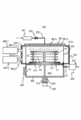
- FIG. 1 It is a schematic block diagram of the single wafer processing furnace of the substrate processing apparatus used suitably by 1st Embodiment in this invention, and is a figure which shows a processing furnace part with a longitudinal cross-sectional view. It is a schematic block diagram of the controller of the substrate processing apparatus used suitably by this invention. It is a figure which shows the flow of the substrate processing in this invention. It is the figure which showed the relationship between the carrier density and temperature of the board
- (B) It is the figure which showed an example of the relationship between the supply timing of a cooling gas, and the process chamber temperature in the 1st Embodiment of this invention.
- (A) It is the figure which showed the modification 1 of 1st Embodiment in this invention.
- (B) It is the figure which showed the modification 2 of 1st Embodiment in this invention.
- A) It is the figure which showed the modification 1 of 2nd Embodiment in this invention.
- (B) It is the figure which showed the modification 2 of 2nd Embodiment in this invention.
- the substrate processing apparatus 100 is configured as a single wafer heat treatment apparatus that performs various heat treatments on a wafer.
- a substrate processing apparatus 100 includes a case 102 as a cavity made of a material that reflects electromagnetic waves such as metal, and an upper and lower ends in a vertical direction that are accommodated in the case 102. It has a cylindrical reaction tube 103 whose part is open.
- the reaction tube 103 is made of a material that transmits electromagnetic waves, such as quartz.
- a cap flange (blocking plate) 104 made of a metal material is brought into contact with the upper end of the reaction tube 103 through an O-ring 220 as a sealing member (seal member) to close the upper end of the reaction tube.
- a processing vessel for processing a substrate such as a silicon wafer is mainly constituted by the case 102, the reaction tube 103, and the cap flange 104.
- the inner space of the reaction tube 103 is constituted as a processing chamber 201.
- a mounting table 210 is provided below the reaction tube 103, and a boat 217 serving as a substrate holder for holding the wafers 200 is mounted on the upper surface of the mounting table 210.
- a boat 217 serving as a substrate holder for holding the wafers 200 is mounted on the upper surface of the mounting table 210.
- the wafers 200 are respectively held above and below the wafer 200 so as to sandwich the wafers 200 at a predetermined interval.
- a not-shown protruding portion that protrudes in the radial direction of the mounting table 210 is provided on the bottom surface side of the mounting table 210.
- the protruding portion approaches or contacts a not-shown squeezing plate provided between the processing chamber 201 and a later-described transfer space 203, the atmosphere in the processing chamber 201 moves into the transfer space 203, or the transfer space.
- the atmosphere in 203 is prevented from moving into the processing chamber 201.
- a plurality of the heat insulating plates 101a and 101b may be installed according to the substrate processing temperature.
- the end plate (ceiling plate) of the boat 217 is provided with a measurement window for the temperature sensor 263.
- the surface temperature of the heat insulating plate 101a is measured by the temperature sensor 263, and the wafer 200 is measured based on the measured temperature.
- the processing temperature is controlled.
- the case 102 as an upper container has a circular cross section, for example, and is configured as a flat sealed container.
- the transport container 202 as a lower container is made of, for example, a metal material such as aluminum (Al) or stainless steel (SUS), quartz, or the like.
- a transfer space 203 for transferring a wafer 200 such as a silicon wafer as a substrate is formed below the processing container.
- a space surrounded by the case 102 or a space surrounded by the reaction tube 103 and above the bottom of the case 102 is referred to as a processing chamber 201 or a reaction area 201 and is surrounded by the transfer container 202.
- the space below the bottom of the case 102 may be referred to as a transfer area 203.
- a substrate loading / unloading port 206 adjacent to the gate valve 205 is provided on the side surface of the transfer container 202, and the wafer 2 moves between a substrate transfer chamber (not shown) via the substrate loading / unloading port 206.
- electromagnetic wave introduction ports 653-1 and 653-2 are formed on the side surface of the case 102.
- One end of waveguides 654-1 and 654-2 for supplying microwaves into the processing chamber 201 is connected to each of the electromagnetic wave introduction ports 653-1 and 653-2.
- microwave oscillators electromagnettic wave sources
- 655-1 and 655-2 are connected to the other ends of the waveguides 654-1 and 654-2 as heating sources for supplying and heating the electromagnetic wave into the processing chamber 201, respectively.
- the electromagnetic wave introduction ports 653-1 and 653-2, the waveguides 654-1 and 654-2, and the microwave oscillators 655-1 and 655-2 are respectively described in the general description.
- the electromagnetic wave introduction port 653, the waveguide 654, and the microwave oscillator 655 are representatively described.
- the mounting table 210 is supported by a shaft 255 as a rotating shaft.
- the shaft 255 passes through the bottom of the transport container 202 and is connected to a drive mechanism 267 that rotates and moves up and down outside the transport container 202.
- a drive mechanism 267 that rotates and moves up and down outside the transport container 202.
- the periphery of the lower end of the shaft 255 is covered with a bellows 212, and the processing space 201 and the conveyance space 203 are kept airtight.
- the mounting table 210 When the wafer 200 is transferred, the mounting table 210 is lowered so that the upper surface of the mounting table is positioned at the substrate loading / unloading port 206 (wafer transfer position). When the wafer 200 is processed, as shown in FIG. It moves up to a processing position (wafer processing position) in 201.
- An exhaust unit that exhausts the atmosphere of the processing chamber 201 is provided below the processing chamber 201 and on the outer peripheral side of the mounting table 210. As shown in FIG. 1, an exhaust port 221 is provided in the exhaust part. An exhaust pipe 231 is connected to the exhaust port 221, and a pressure regulator 244 such as an APC valve that controls the valve opening degree according to the pressure in the processing chamber 201 and a vacuum pump 246 are connected in series to the exhaust pipe 231. It is connected to the.
- the pressure regulator 244 is not limited to an APC valve as long as it can receive pressure information in the processing chamber 201 (a feedback signal from a pressure sensor 245 described later) and adjust the exhaust amount.
- the on-off valve and the pressure regulating valve may be used in combination.
- the exhaust port 221, the exhaust pipe 231, and the pressure regulator 244 mainly constitute an exhaust part (also referred to as an exhaust system or an exhaust line).
- an exhaust path may be provided so as to surround the processing chamber 201 so that gas can be exhausted from the entire periphery of the wafer 200.
- a nozzle 105 for supplying processing gases for processing various substrates such as an inert gas, a raw material gas, and a reactive gas into the processing chamber 201 is provided through the lower surface of the case 102.
- a gas supply hole 105 a for supplying gas is provided on the side surface of the nozzle 105.
- the gas supply hole 105 a is opened so as to face the center of the wafer 200, and supplies gas in parallel with the surface of the wafer 200.
- a plurality of the gas supply holes 105a are provided from the lower part to the upper part of the reaction tube 103, each having the same opening area, and further provided at the same opening pitch.
- a gas supply pipe 232 is connected to the nozzle 105.
- the gas supply pipe 232 is provided with a mass flow controller (MFC) 241 that is a flow rate controller (flow rate control unit) and a valve 243 that is an on-off valve in order from the upstream side.
- MFC mass flow controller
- N 2 nitrogen
- a supply pipe may be connected, or a plurality of nozzles may be provided independently according to the type of gas used.
- a gas supply unit (also referred to as a gas supply system) is mainly configured by the gas supply pipe 232, the MFC 241, and the valve 243.
- an inert gas supply unit (also referred to as an inert gas supply system) is mainly configured by the gas supply pipe 232, the MFC 241, and the valve 243.
- the inert gas for example, a rare gas such as Ar gas, He gas, Ne gas, or Xe gas can be used in addition to N 2 gas.
- the cap flange 104 is provided with a temperature sensor 263 as a non-contact type temperature detector.
- a temperature sensor 263 By adjusting the output of a microwave oscillator 655, which will be described later, based on the temperature information detected by the temperature sensor 263, the substrate is heated, and the substrate temperature has a desired temperature distribution.
- the temperature sensor 263 is configured by a radiation thermometer such as an IR (Infrared Radiation) sensor.
- the method for measuring the temperature of the substrate is not limited to the above-described radiation thermometer, and temperature measurement may be performed using a thermocouple, or temperature measurement may be performed using both a thermocouple and a radiation thermometer. Good.
- thermocouple when temperature measurement is performed using a thermocouple, it is necessary to perform temperature measurement by placing the thermocouple in the vicinity of the processing wafer 200 in order to improve the temperature measurement accuracy of the thermocouple. Since the thermocouple itself is heated by the supplied microwave, it is preferable to use a radiation thermometer as the temperature sensor 263. Further, the temperature sensor 263 is not limited to being provided on the cap flange 104 but may be provided on the mounting table 210. With such a configuration, it is possible to use a reaction tube whose upper end is closed, and it is possible to reduce the possibility of leakage of microwaves, processing gas, and the like supplied to the processing chamber 201.
- the temperature sensor 263 is not only directly installed on the cap flange 104 or the mounting table 210 but also indirectly measured by reflecting the radiated light from the measurement window provided on the cap flange 104 or the mounting table 210 with a mirror or the like. It may be configured to. With this configuration, it is possible to relax restrictions on the place where the temperature sensor 263 is installed.
- Electromagnetic wave introduction ports 653-1 and 653-2 are installed on the side wall of the case 102.
- One end of each of waveguides 654-1 and 654-2 for supplying electromagnetic waves into the processing chamber 201 is connected to each of the electromagnetic wave introduction ports 653-1 and 653-2.
- microwave oscillators electromagnettic wave sources
- the microwave oscillators 655-1 and 655-2 supply electromagnetic waves such as microwaves to the waveguides 654-1 and 654-2, respectively.
- the frequency of the electromagnetic wave generated by the microwave oscillator 655 is preferably controlled to be in the frequency range of 13.56 MHz to 24.125 GHz. More preferably, the frequency is preferably controlled to be 2.45 GHz or 5.8 GHz.
- two microwave oscillators 655 are described as being disposed on the side surface of the case 102, but the present invention is not limited to this, and one or more microwave oscillators may be provided. Further, the microwave oscillator 655 may be disposed so as to be provided on different side surfaces such as the opposite side surfaces of the case 102.
- the microwave generators 655-1 and 655-2, the waveguides 654-1 and 654-2, and the electromagnetic wave introduction ports 653-1 and 653-2 are used to supply a microwave (an electromagnetic wave supply device, an electromagnetic wave supply unit, a micro wave).
- a heating device as a wave supply device) is configured.
- a controller 121 (to be described later) is connected to each of the microwave oscillators 655-1 and 655-2.
- the controller 121 is connected to a heat insulating plate 101 a or 101 b housed in the processing chamber 201 or a temperature sensor 263 that measures the temperature of the wafer 200.
- the temperature sensor 263 measures the temperature of the heat insulating plate 101a or 101b or the wafer 200 and transmits it to the controller 121.
- the controller 121 controls the output of the microwave oscillators 655-1 and 655-2 to control the heating of the wafer 200. Control.
- the microwave oscillators 655-1 and 655-2 are controlled by the same control signal transmitted from the controller 121.
- the present invention is not limited to this, and the microwave oscillators 655-1 and 655-2 are individually controlled by transmitting individual control signals from the controller 121 to the microwave oscillators 655-1 and 655-2, respectively. May be.
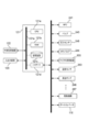
- the controller 121 which is a control unit (control means), is configured as a computer including a CPU (Central Processing Unit) 121a, a RAM (Random Access Memory) 121b, a storage device 121c, and an I / O port 121d.
- the RAM 121b, the storage device 121c, and the I / O port 121d are configured to exchange data with the CPU 121a via the internal bus 121e.
- an input / output device 122 configured as a touch panel or the like is connected to the controller 121.
- the storage device 121c includes, for example, a flash memory, an HDD (Hard Disk Drive), and the like.
- a control program for controlling the operation of the substrate processing apparatus, and an etching recipe and a process recipe that describe the later-described nozzle etching process and film forming process procedures and conditions are stored in a readable manner.
- the etching recipe and the process recipe are combined so that a predetermined result can be obtained by causing the controller 121 to execute each procedure in the substrate processing process described later, and functions as a program.
- the process recipe, the control program, and the like are collectively referred to simply as a program.
- An etching recipe or a process recipe is also simply called a recipe.
- the RAM 121b is configured as a memory area (work area) in which programs, data, and the like read by the CPU 121a are temporarily stored.
- the I / O port 121d is connected to the above-described MFCs 241a to 241d, valves 243a to 243d, pressure sensor 245, APC valve 244, vacuum pump 246, temperature sensor 263, drive mechanism 267, microwave oscillator 655, and the like.
- the CPU 121a is configured to read and execute a control program from the storage device 121c and to read a recipe from the storage device 121c in response to an operation command input from the input / output device 122 or the like.
- the CPU 121a adjusts the flow rate of various gases by the MFCs 241a to 241d, the opening / closing operation of the valves 243a to 243d, the opening / closing operation of the APC valve 244, and the pressure adjustment by the APC valve 244 based on the pressure sensor 245 so as to follow the contents of the read recipe.
- Control of operation, start and stop of vacuum pump 246, output adjustment operation of microwave oscillator based on temperature sensor 263, rotation and rotation speed adjustment operation of mounting table 210 (or boat 217) by driving mechanism 267, or raising / lowering operation, etc. Is configured to do.
- the controller 121 is stored in an external storage device 123 (for example, a magnetic tape, a magnetic disk such as a flexible disk or a hard disk, an optical disk such as a CD or a DVD, a magneto-optical disk such as an MO, or a semiconductor memory such as a USB memory or a memory card).
- the above-mentioned program can be configured by installing it in a computer.
- the storage device 121c and the external storage device 123 are configured as computer-readable recording media. Hereinafter, these are collectively referred to simply as a recording medium.
- recording medium When the term “recording medium” is used in this specification, it may include only the storage device 121c alone, may include only the external storage device 123 alone, or may include both.
- the program may be provided to the computer using a communication means such as the Internet or a dedicated line without using the external storage device 123.
- wafer when the term “wafer” is used in this specification, it means “wafer (product wafer) itself” or “lamination of a wafer and a predetermined layer or film formed on the surface thereof”.
- body that is, when referring to a wafer including a predetermined layer or film formed on the surface, a “target substrate (target wafer)” to be described later or a “dummy substrate (dummy wafer) to be described later ) "Or” both target substrate (target wafer) and dummy substrate (dummy wafer) ".
- wafer surface means “the surface of the wafer itself (exposed surface)” using the definition of “wafer” described above, or “formed on the wafer”. It may mean the surface of the predetermined layer or film, that is, the outermost surface of the wafer as a laminate.
- the predetermined gas is applied to the surface (exposed surface) of the wafer itself, using the definition of“ wafer ”described above. It means “to supply” or “to supply a predetermined gas to a layer or film formed on the wafer, that is, to the outermost surface of the wafer as a laminated body”. There is a case. Further, in this specification, when “describe a predetermined layer (or film) on the wafer” is described, “determine a predetermined layer (or film) on the surface (exposed surface) of the wafer itself”. , Or “to form a predetermined layer (or film) on the layer or film formed on the wafer, that is, on the outermost surface of the wafer as a laminate” There is.
- substrate is also synonymous with the term “wafer”.
- the drive mechanism 267 rotates the shaft 255 and rotates the wafer 200 via the boat 217 on the mounting table 210.
- an inert gas such as nitrogen gas is supplied from the nozzle 105 via the gas supply pipe 232 (S303).
- the pressure in the processing chamber 201 is a predetermined value in the range of 0 Pa to 200,000 Pa, and is adjusted to be, for example, 101300 Pa to 101,566 Pa.
- the microwave oscillators 655-1 and 655-2 cause the wafer 200 to have a temperature range of 100 ° C. to 700 ° C., preferably 200 ° C. to 600 ° C. It heats so that it may become a belt
- the wafer 200 becomes difficult to absorb the microwave, and the wafer 200 is efficiently heated. It becomes impossible to do.
- the temperature of the wafer 200 is estimated based on temperature conversion data stored in advance in the storage device 121 c or the external storage device 122 from the value obtained by measuring the surface temperature of the quartz susceptor 101 a with the temperature sensor 263.
- the microwave oscillators 655-1 and 655-2 supply microwaves from the electromagnetic wave introduction ports 653-1 and 653-2 into the processing chamber 201 via the waveguides 654-1 and 654-2. Since the microwave supplied into the processing chamber 201 enters the wafer 200 and is efficiently absorbed, the wafer 200 can be heated extremely effectively.
- the processing temperature is maintained for a predetermined time.
- the microwave oscillator 655 By controlling the microwave oscillator 655 in this manner, the amorphous silicon film formed on the surface of the microwave wafer 200 is modified.
- the microwave oscillators 655-1 and 655-2 can be controlled to increase the outputs of the microwave oscillators 655-1 and 655-2 while intermittently supplying the microwaves.
- the pulse control for intermittently supplying the microwave supply from the microwave oscillator and the power limit control for linearly controlling the outputs of the microwave oscillators 655-1 and 655-2 may be performed in combination.
- a standing wave is formed in the processing chamber 201 by supplying a pulsed microwave when the temperature of the wafer 200 is raised, and the region is heated by being concentrated on the wafer surface (microwave concentration region, hot spot). ) Is formed, a time during which the microwave is not supplied (OFF time) can be provided.
- the carrier density and carrier temperature dependence of the wafer 200 As shown in FIG. 4, when an example of the temperature dependence of the carrier density of the wafer 200 with the vertical axis representing carrier density (proportional to conductivity) and the horizontal axis representing temperature, the region (A) and the region depend on the temperature. It can be divided into (B) and region (C).
- the temperature that separates the regions (A) and (B) is 327 ° C.
- the temperature that separates the regions (B) and (C) is ⁇ 73 ° C.
- regions (A) and (C) the carrier density greatly increases as the temperature rises, but in region (B), the carrier density greatly increases even when the temperature rises. do not do.
- the amount of heat generated per unit time of the wafer 200 is proportional to the carrier density of the wafer 200, when the carrier density changes, the amount of generated heat also changes accordingly. For this reason, when microwave heating is performed in the region (A) where the change in carrier density is large, the rate at which the carrier density increases according to the temperature change is large. The heating rate of 200 increases. Therefore, it is preferable that heating by microwaves is performed in the region (A).
- the heating rate of the wafer 200 since the heating rate of the wafer 200 is large as described above, when the microwaves are locally concentrated, the concentrated portion becomes high temperature, and the temperature difference is partially large in the plane of the wafer 200. Thus, the wafer 200 is deformed due to the difference in thermal expansion. Therefore, by cooling the wafer 200 while performing microwave heating in the temperature zone of the region (A), it is possible to reduce the in-plane temperature difference of the wafer 200 and suppress the wafer 200 from being deformed. It becomes possible to improve the reforming treatment speed.
- an inert gas for example, N 2 gas
- N 2 gas an inert gas
- the MFC 241 is set so that the flow rate of the inert gas (N 2 gas) as the cooling gas at the timing when the microwave oscillator 655 is turned on is 0.1 slm or more and 10 slm or less.
- the wafer 200 can be maintained in a constant temperature range.
- the flow rate of the cooling gas supplied at the timing when the microwave oscillator 655 is turned on is set to 0.1 slm or less, the pressure in the processing chamber 201 may drop when the microwave is supplied, and plasma discharge may occur. . If plasma discharge occurs in the processing chamber 201, the wafer 200 may be damaged by the plasma discharge.
- the flow rate of the cooling gas supplied at the timing when the microwave oscillator 655 is turned ON is set to 10 slm or more, the wafer 200 cannot be heated and the substrate processing cannot be performed efficiently. End up.
- the flow rate of the cooling gas supplied at the timing when the microwave oscillator 655 is turned off is set to 0.1 slm or less, the wafer 200 cannot be efficiently cooled, and the substrate processing time becomes long.
- the flow rate of the cooling gas supplied at the timing when the microwave oscillator 655 is turned off is set to 30 slm or more, the pressure in the processing chamber 201 becomes excessively pressurized, and the wafer 200 and the processing apparatus are damaged. There is a possibility that it will end up.
- the temperature of the wafer 200 can be maintained at an optimum temperature.
- the gas supply unit and the exhaust unit may be controlled so as to increase or decrease the pressure in the processing chamber 201 in accordance with the timing of increasing or decreasing the gas supply flow rate. That is, at the timing when the microwave oscillator 655 is ON, the pressure in the processing chamber 201 is controlled to be a predetermined pressure suitable for substrate processing, and at the timing when the microwave oscillator 655 is OFF.
- the control of the substrate processing process can be simplified by not controlling the pressure in the processing chamber 201, that is, by turning off the control of the exhaust part (particularly the pressure adjusting part 244).
- the MFC 241 is controlled to supply 5 slm of cooling gas, and the pressure in the processing chamber 201 is 101300 Pa (or 101300 Pa or more).
- the pressure regulator 244 is controlled to be within a range of 101,566 Pa or less.
- the MFC 241 is controlled to control the cooling gas, the cooling gas is supplied by 15 slm, and the pressure adjusting unit 244 is turned OFF. Controls the microwave supply unit and the gas supply unit so that the pressure is increased to about 101966 Pa (or a range of 101433 Pa or more and 102232 Pa or less) by the supply of the cooling gas.
- the processing chamber 201 is suppressed to a pressure lower than the pressure at which a problem such as over-pressurization occurs by controlling the supply flow rate of the cooling gas. Therefore, it is effective when processing that does not require detailed control of pressure is performed.
- the gas supply unit may be controlled according to the temperature measured by the temperature sensor 263 or the temperature estimated by the previously stored temperature conversion data. . That is, the microwave oscillator 655 is always turned on, and gas is supplied at a timing when the temperature of the heated wafer 200 becomes higher than a predetermined target temperature (a temperature that becomes a threshold value, for example, 400 ° C. in FIG. 5B).
- the wafer 200 is cooled by increasing the flow rate of the cooling gas by increasing the opening of the MFC 241, specifically, the MFC 241.
- the opening degree of the MFC 241 is decreased, the flow rate of the cooling gas is decreased, and the wafer 200 is heated.
- the pulse width is, for example, 1 ⁇ 10 ⁇ 4 sec. It is preferable to be able to control at intervals. With this configuration, accurate temperature control can be performed both during wafer temperature rise and during wafer processing. Note that the pulse width may be controlled to be different between when the wafer is heated and when the wafer is processed. With this configuration, the temperature difference between the microwave concentration region on the surface of the wafer 200 and the other surface is likely to increase (the region other than the microwave concentration region is not heated). By making it smaller, the in-plane temperature uniformity can be improved.
- the temperature difference between the microwave concentration region and the other surface on the surface of the wafer 200 is unlikely to be large (the region other than the microwave concentration region is heated to some extent). It becomes possible to sufficiently irradiate the wafer surface with microwaves, and it is possible to perform sufficient wafer processing. Further, the time interval between the ON time and the OFF time of the pulse width may be controlled to be different. As described above, the heat treatment of the wafer 200 causes the amorphous silicon film formed on the surface of the wafer 200 to be modified (crystallized) into a polysilicon film. That is, the wafer 200 can be uniformly modified (S304).
- an inert gas such as N 2 gas is supplied, and the pressure in the processing chamber 201 is returned to atmospheric pressure.
- Substrate unloading step (S305) After returning the pressure in the processing chamber 201 to atmospheric pressure, the drive mechanism 267 lowers the mounting table 210 to open the furnace port and unload the boat 217 into the transfer space 203 (boat unloading). Thereafter, the wafer 200 placed on the boat is carried out to a transfer chamber located outside the transfer space 203 (S305). By repeating the above operation, the wafer 200 is modified.
- the wafer temperature can be maintained at a predetermined temperature, and the wafer temperature can be increased efficiently.
- the wafer temperature can be efficiently maintained by increasing or decreasing the flow rate of the inert gas in conjunction with the on / off of the microwave oscillator.
- the substrate processing apparatus in the present embodiment is not limited to the above-described aspect, and can be modified as in the following modification.
- the first modification of the first embodiment is configured such that a boat 217 can hold a plurality of wafers 200 in multiple stages.
- a plurality of wafers 200 are configured to be held in multiple horizontal stages at predetermined intervals between the heat insulating plates 101a and 101b held on the boat 217, and held in the order of the substrate processing steps described above.
- a plurality of wafers 200 are processed uniformly. With this configuration, a plurality of wafers 200 can be processed in a single process, and the throughput of substrate processing can be improved.
- the plurality of wafers 200 are held so as to be sandwiched between the heat insulating plates 101a and 101b.
- each of the plurality of wafers 200 is fixed to the plurality of heat insulating plates 101a. , 101b may be sandwiched and held. In this case, a plurality of heat insulating plates 101a and 101b are also provided. By configuring in this way, it becomes possible not only to heat the wafer 200 faster than in the first embodiment, but also to improve the temperature uniformity within the wafer surface.
- the second modification of the first embodiment is configured such that an exhaust nozzle 601 for exhaust is installed at a position facing the nozzle 105 with the boat 217 interposed therebetween.
- An exhaust port for exhausting the atmosphere in the processing chamber 201 is provided on the side surface of the exhaust nozzle 601 facing the gas supply nozzle side, and an exhaust pipe 231 is connected to the downstream side of the exhaust nozzle 601.
- the substrate processing apparatus is different from the first embodiment in that the gas supply unit penetrates the cap flange 104 without providing the gas supply nozzle, as shown in FIG.
- a cooling gas is supplied from above the wafer, and a gas rectifying unit 700 that suppresses direct injection of the cooling gas to the upper end plate (also referred to as a top plate) of the boat 217.
- components having the same functions as those in the first embodiment are denoted by the same reference numerals, and description thereof is omitted.
- a gas supply pipe 232 is installed so as to penetrate the cap flange 104 provided above the processing chamber 201, and a gas supply port 703 provided above the processing chamber 201. Cooling gas is supplied from At a position facing the gas supply port 703 provided above the processing chamber 201, the temperature of the boat 217 is locally cooled when the cooling gas directly hits the boat 217, so that the in-plane temperature uniformity of the wafer 200 is achieved.
- a gas rectifying unit 700 including a gas rectifying plate 701 that rectifies a gas flow and a fixing unit 702 for fixing the gas rectifying plate 701 to the cap flange 104 is provided.
- the gas rectifying unit 700 is provided at a position facing the gas supply port 703 so that the cooling gas supplied from the substantially central portion of the cap flange 104 flows from the outer peripheral side of the gas rectifying plate 701. It is possible to control the cooling gas to flow to a desired position by changing the diameter of the gas rectifying plate 701.
- the gas rectifying plate 701 is formed in a disk shape having a diameter larger than the outer diameter of the top plate of the boat 217, and is configured such that the cooling gas flows on the outer periphery of the boat 217. With this configuration, the control of the gas supply unit can be simplified as compared with the first embodiment without complicating the device structure. In addition, since it is possible to cool uniformly from the outer periphery of the wafer, the in-plane temperature uniformity of the wafer 200 can be improved.
- the substrate processing apparatus in the present embodiment is not limited to the above-described aspect, and can be changed as in the following modification.
- Modification 1 As shown in FIG. 8A, in the first modification of the second embodiment, the height of the boat 217 is increased, and the top plate portion of the boat 217 functions as a gas rectifier, so that the cooling gas is transferred to the wafer.
- the in-plane temperature uniformity of 200 is suppressed from being affected. With this configuration, it is not necessary to install a new part in the processing chamber, so that not only the cost is reduced but also the generation of particles can be suppressed.
- Modification 2 As shown in FIG. 8B, in the second modification of the second embodiment, the height direction of the boat 217 is increased as in the first modification, and the top plate portion of the boat 217 functions as a gas rectifying unit.
- the heat insulating plates 801-1 and 801-2 are held by the boat 217 so as to be positioned above the heat insulating plate 101a.
- the heat insulating plates 801-1 and 801-2 may be the same as the heat insulating plates 101a and 101b, or may have different materials and heat insulating properties.
- the substrate processing apparatus according to the present invention is different from the first and second embodiments in that a shower head is provided above the processing chamber 201 as shown in FIG. It is a point to supply.
- a shower head is provided above the processing chamber 201 as shown in FIG. It is a point to supply.
- components having the same functions as those in the first embodiment are denoted by the same reference numerals, and description thereof is omitted.
- a shower head 901 is installed at the downstream end of the gas supply pipe 232, and the cooling gas is dispersed from the dispersion plate 901 a of the shower head 901 so that the processing chamber 201 is directed downward from above. A gas flow is formed.
- the shower head 901 supplies the cooling gas supplied from the gas supply pipe 232 through a plurality of gas supply ports 901b provided in the dispersion plate 901a.
- the shower head 901 can form a desired gas flow by changing the installation position and number of the gas supply ports 901b provided in the dispersion plate 901 and the supply area of the gas supply ports.
- the gas supply port 901 provided on the outermost side is formed so as to be provided outside the outer diameter of the top plate of the boat 217, so that the cooling gas flows also on the outer peripheral side of the boat 217. With this configuration, even when the cooling gas is directly supplied to the top plate of the boat 217, the cooling gas can be supplied in a distributed manner, which affects the modification process of the wafer 200. It is possible to suppress cooling to such an extent that
- the process of modifying an amorphous silicon film into a polysilicon film as a film containing silicon as a main component has been described.
- the present invention is not limited to this, and oxygen (O), nitrogen (N ), Carbon (C), and hydrogen (H) may be supplied to supply a gas containing at least one or more to modify the film formed on the surface of the wafer 200.
- hafnium oxide film As a high dielectric film is formed on the wafer 200, by supplying a microwave and heating while supplying a gas containing oxygen, the hafnium oxide film The non-crystallized portion in the hafnium oxide film is replenished with oxygen and improved in characteristics of the high dielectric film, or heated by supplying a microwave while supplying nitrogen gas (N 2 gas). And the characteristics of the high dielectric film can be improved.
- the hafnium oxide film is shown here, the present invention is not limited to this, and at least one of Al, Ti, Zr, Ta, Nb, La, Ce, Y, Ba, Sr, Ca, Pb, Mo, W, etc.
- the present invention can also be suitably applied to the case of forming an oxide film containing a metal element containing metal, that is, a metal-based oxide film. That is, the above-described film forming sequence is performed on the wafer 200 on the Ti film, the TiN film, the TiOCN film, the TiOC film, the TiON film, the TiO film, the ZrN film, the ZrOCN film, the ZrOC film, the ZrON film, the ZrO film, the HfOCN film, HfOC film, HfON film, HfO film, TaOCN film, TaOC film, TaON film, TaO film, NbOCN film, NbOC film, NbON film, NbO film, AlOCN film, AlOC film, AlON film, AlO film, MoOCN film, MoOC film
- the present invention can also be suitably applied to the formation of MoON films, MoO films, W films, WOCN films, WOC films, WON films, and WO films.
- the film containing silicon as a main component examples include Si-based oxide films such as SiN films, SiO films, SiOC films, SiOCN films, and SiON films, Epi-Si films, and Epi-SiGe films.
- the impurity examples include at least one of B, C, N, Al, P, Ga, As, and the like.
- an Epi-Ge film or a film formed using a Group 3-5 element may be heated.
- a resist film based on at least one of methyl methacrylate resin (PMMA), epoxy resin, novolac resin, polyvinyl phenyl resin, and the like may be used.
- the present invention is not limited to this. Patterning process in the liquid crystal panel manufacturing process, patterning process in the solar cell manufacturing process, and patterning process in the power device manufacturing process.
- the present invention can also be applied to a technique for processing a substrate.
- the present invention can provide a technique that enables uniform substrate processing.
- Substrate processing apparatus 101a, 101b ... heat insulating plates (quartz plate, Si plate) 102 ... Case (cavity), 103 ... reaction tube, 105 ... Nozzle, 121... Controller (control unit), 200: Wafer (substrate), 201 ... processing chamber, 217 ... Boat (substrate holder), 655 ... Microwave oscillator (heating device).
Abstract
基板と断熱板を保持する基板保持具が搬入されて前記基板を処理する処理室と、前記処理室内にマイクロ波を供給するマイクロ波供給部を有する加熱装置と、前記処理室内に冷却ガスを供給するガス供給部と、前記加熱装置によって前記基板を加熱する加熱時に前記ガス供給部から冷却ガスを供給することで前記基板を所定の温度に維持するように前記加熱装置と前記ガス供給部とを制御するよう構成される制御部とを有する技術が提供できる。
Description
本発明は、基板処理装置、半導体装置の製造方法および記録媒体に関するものである。
半導体装置の製造工程の一工程として、例えば、加熱装置を用いて処理室内の基板を加熱し、基板の表面に成膜された薄膜中の組成や結晶構造を変化させるアニール処理がある。近年の半導体デバイスにおいては、微細化に伴い、高いアスペクト比を有するパターンが形成された高密度の基板へのアニール処理が求められている。
従来のアニール処理では、基板を均一に加熱することができず、対象膜の均一な処理ができなかった。
本発明の目的は、均一な基板処理を行うことが可能となる技術を提供することにある。
本発明の一態様によれば、
基板と断熱板を保持する基板保持具が搬入されて前記基板を処理する処理室と、
前記処理室内にマイクロ波を供給するマイクロ波供給部を有する加熱装置と、
前記処理室内に冷却ガスを供給するガス供給部と、
前記加熱装置によって前記基板を加熱する加熱時に前記ガス供給部から冷却ガスを供給することで前記基板を所定の温度に維持するように前記加熱装置と前記ガス供給部とを制御するよう構成される制御部と
を有する技術が提供される。
基板と断熱板を保持する基板保持具が搬入されて前記基板を処理する処理室と、
前記処理室内にマイクロ波を供給するマイクロ波供給部を有する加熱装置と、
前記処理室内に冷却ガスを供給するガス供給部と、
前記加熱装置によって前記基板を加熱する加熱時に前記ガス供給部から冷却ガスを供給することで前記基板を所定の温度に維持するように前記加熱装置と前記ガス供給部とを制御するよう構成される制御部と
を有する技術が提供される。
本発明によれば、均一な基板処理を行うことが可能となる技術を提供することができる。
<本発明の第1の実施形態>
以下に本発明の第1の実施形態を図面に基づいて説明する。
以下に本発明の第1の実施形態を図面に基づいて説明する。
(1)基板処理装置の構成
本実施の形態において、本発明に係る基板処理装置100は、ウエハに各種の熱処理を施す枚葉式熱処理装置として構成されている。
本実施の形態において、本発明に係る基板処理装置100は、ウエハに各種の熱処理を施す枚葉式熱処理装置として構成されている。
(処理室)
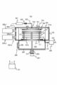
図1に示すように、本実施形態に係る基板処理装置100は、金属などの電磁波を反射する材料で構成されるキャビティとしてのケース102と、ケース102の内部に収容され、垂直方向の上下端部が開放された筒形状の反応管103を有している。反応管103は、石英などの電磁波を透過する材料で構成される。また、金属材料で構成されたキャップフランジ(閉塞板)104が、封止部材(シール部材)としてのOリング220を介して反応管103の上端と当接されて反応管の上端を閉塞する。主にケース102と反応管103、および、キャップフランジ104によってシリコンウエハ等の基板を処理する処理容器を構成し、特に反応管103の内側空間を処理室201として構成している。
図1に示すように、本実施形態に係る基板処理装置100は、金属などの電磁波を反射する材料で構成されるキャビティとしてのケース102と、ケース102の内部に収容され、垂直方向の上下端部が開放された筒形状の反応管103を有している。反応管103は、石英などの電磁波を透過する材料で構成される。また、金属材料で構成されたキャップフランジ(閉塞板)104が、封止部材(シール部材)としてのOリング220を介して反応管103の上端と当接されて反応管の上端を閉塞する。主にケース102と反応管103、および、キャップフランジ104によってシリコンウエハ等の基板を処理する処理容器を構成し、特に反応管103の内側空間を処理室201として構成している。
反応管103の下方には載置台210が設けられており、載置台210の上面には、ウエハ200を保持する基板保持具としてのボート217が載置されている。ボート217には、処理対象としてのウエハ200と、例えばダミーウエハなどの石英板やシリコンプレート(Si板)などで形成されたウエハ200の温度を維持(保温)するための断熱板101a、101bが、所定の間隔でウエハ200を挟み込むようにウエハ200の上下にそれぞれ保持されている。また、載置台210の側壁には、載置台210の径方向に向かって突出した図示しない突出部が載置台210の底面側に設けられる。この突出部が、処理室201と後述する搬送空間203との間に設けられる図示しないしきり板と接近または接触することで処理室201内の雰囲気が搬送空間203内へ移動することや、搬送空間203内の雰囲気が処理室201内へ移動することを抑制する。
ここで、断熱板101a、101bは基板処理温度に応じて複数枚ずつ設置してもよい。このように複数枚ずつ設置することによってウエハ200が載置されている領域において放熱されることを抑制することが可能となり、ウエハ200の面内または面間温度均一性を向上させることが可能となる。また、ボート217の端板(天井板)には、温度センサ263の測定窓が設けられており、温度センサ263によって断熱板101aの表面温度が測定され、測定された温度に基づいてウエハ200の処理温度が制御される。
ここで、断熱板101a、101bは基板処理温度に応じて複数枚ずつ設置してもよい。このように複数枚ずつ設置することによってウエハ200が載置されている領域において放熱されることを抑制することが可能となり、ウエハ200の面内または面間温度均一性を向上させることが可能となる。また、ボート217の端板(天井板)には、温度センサ263の測定窓が設けられており、温度センサ263によって断熱板101aの表面温度が測定され、測定された温度に基づいてウエハ200の処理温度が制御される。
上部容器としてのケース102は、例えば横断面が円形であり、平らな密閉容器として構成されている。また、下部容器としての搬送容器202は、例えばアルミニウム(Al)やステンレス(SUS)などの金属材料または、石英などにより構成されている。処理容器の下方には、基板としてのシリコンウエハ等のウエハ200を搬送する搬送空間203が形成されている。なお、ケース102に囲まれた空間、または、反応管103に囲まれた空間であって、ケース102の底部よりも上方の空間を処理室201又は反応エリア201と称し、搬送容器202に囲まれた空間であって、ケース102の底部よりも下方の空間を搬送エリア203と称する場合もある。
搬送容器202の側面には、ゲートバルブ205に隣接した基板搬入出口206が設けられており、ウエハ2は基板搬入出口206を介して図示しない基板搬送室との間を移動する。
ケース102の側面には、電磁波導入ポート653-1、653-2が穿設されている。電磁波導入ポート653-1、653-2のそれぞれには処理室201内にマイクロ波を供給するための導波管654-1、654-2の一端が接続されている。導波管654-1、654-2の他端のそれぞれには処理室201内に電磁波を供給して加熱する加熱源としてのマイクロ波発振器(電磁波源)655-1、655-2が接続されている。
ここで、電磁波導入ポート653-1、653-2、導波管654-1、654-2、マイクロ波発振器655-1、655-2は、一般的な説明等をする場合には、それぞれを代表して電磁波導入ポート653、導波管654、マイクロ波発振器655と記載する。
ここで、電磁波導入ポート653-1、653-2、導波管654-1、654-2、マイクロ波発振器655-1、655-2は、一般的な説明等をする場合には、それぞれを代表して電磁波導入ポート653、導波管654、マイクロ波発振器655と記載する。
載置台210は回転軸としてのシャフト255によって支持される。シャフト255は、搬送容器202の底部を貫通しており、更には搬送容器202の外部で回転、昇降動作を行う駆動機構267に接続されている。駆動機構267を作動させてシャフト255及び載置台210を回転、昇降させることにより、ボート217上に載置されるウエハ200を回転または昇降させることが可能となっている。なお、シャフト255下端部の周囲はベローズ212により覆われており、処理空間201および搬送空間203内は気密に保持されている。
載置台210は、ウエハ200の搬送時には、載置台上面が基板搬入出口206の位置(ウエハ搬送位置)となるよう下降し、ウエハ200の処理時には図1で示されるように、ウエハ200が処理室201内の処理位置(ウエハ処理位置)まで上昇する。
(排気部)
処理室201の下方であって、載置台210の外周側には、処理室201の雰囲気を排気する排気部が設けられている。図1に示すように、排気部には排気口221が設けられている。排気口221には排気管231が接続されており、排気管231には、処理室201内の圧力に応じて弁開度を制御するAPCバルブなどの圧力調整器244、真空ポンプ246が順に直列に接続されている。
ここで、圧力調整器244は、処理室201内の圧力情報(後述する圧力センサ245からのフィードバック信号)を受信して排気量を調整することができるものであればAPCバルブに限らず、通常の開閉バルブと圧力調整弁を併用するように構成されていてもよい。
処理室201の下方であって、載置台210の外周側には、処理室201の雰囲気を排気する排気部が設けられている。図1に示すように、排気部には排気口221が設けられている。排気口221には排気管231が接続されており、排気管231には、処理室201内の圧力に応じて弁開度を制御するAPCバルブなどの圧力調整器244、真空ポンプ246が順に直列に接続されている。
ここで、圧力調整器244は、処理室201内の圧力情報(後述する圧力センサ245からのフィードバック信号)を受信して排気量を調整することができるものであればAPCバルブに限らず、通常の開閉バルブと圧力調整弁を併用するように構成されていてもよい。
主に、排気口221、排気管231、圧力調整器244により排気部(排気系または排気ラインとも称する)が構成される。なお、処理室201を囲むように排気路を設け、ウエハ200の全周からガスを排気可能に構成してもよい。また、排気部の構成に、真空ポンプ246を加えるようにしてもよい。
(ガス供給部)
反応管103の内側には不活性ガス、原料ガス、反応ガスなどの各種基板処理のための処理ガスを処理室201内に供給するためのノズル105がケース102の下面を介して設けられている。ノズル105の側面にはガスを供給するガス供給孔105aが設けられている。ガス供給孔105aはウエハ200の中心を向くように開口し、ウエハ200の表面と平行にガスを供給する。このガス供給孔105aは反応管103の下部から上部にわたって複数設けられ、それぞれが同一の開口面積を有し、さらに同じ開口ピッチで設けられている。ノズル105には、ガス供給管232が接続されている。ガス供給管232には、上流から順に、流量制御器(流量制御部)であるマスフローコントローラ(MFC)241、開閉弁であるバルブ243が設けられている。ガス供給管232の上流側には、例えば不活性ガスである窒素(N2)ガス源が接続され、MFC241、バルブ243を介して処理室201内へ供給される。基板処理の際に複数種類のガスを使用する場合には、ガス供給管232のバルブ243よりも下流側に上流方向から順に、流量制御器であるMFCおよび開閉弁であるバルブが設けられたガス供給管が接続されていてもよいし、使用するガスの種類に応じて複数のノズルが独立して設けられるように構成されていても良い。主に、ガス供給管232、MFC241、バルブ243によりガス供給部(ガス供給系とも称する)が構成される。
反応管103の内側には不活性ガス、原料ガス、反応ガスなどの各種基板処理のための処理ガスを処理室201内に供給するためのノズル105がケース102の下面を介して設けられている。ノズル105の側面にはガスを供給するガス供給孔105aが設けられている。ガス供給孔105aはウエハ200の中心を向くように開口し、ウエハ200の表面と平行にガスを供給する。このガス供給孔105aは反応管103の下部から上部にわたって複数設けられ、それぞれが同一の開口面積を有し、さらに同じ開口ピッチで設けられている。ノズル105には、ガス供給管232が接続されている。ガス供給管232には、上流から順に、流量制御器(流量制御部)であるマスフローコントローラ(MFC)241、開閉弁であるバルブ243が設けられている。ガス供給管232の上流側には、例えば不活性ガスである窒素(N2)ガス源が接続され、MFC241、バルブ243を介して処理室201内へ供給される。基板処理の際に複数種類のガスを使用する場合には、ガス供給管232のバルブ243よりも下流側に上流方向から順に、流量制御器であるMFCおよび開閉弁であるバルブが設けられたガス供給管が接続されていてもよいし、使用するガスの種類に応じて複数のノズルが独立して設けられるように構成されていても良い。主に、ガス供給管232、MFC241、バルブ243によりガス供給部(ガス供給系とも称する)が構成される。
ガス供給管232から不活性ガスを供給する場合、主に、ガス供給管232、MFC241、バルブ243により不活性ガス供給部(不活性ガス供給系とも称する)が構成される。不活性ガスとしては、N2ガスの他、例えば、Arガス、Heガス、Neガス、Xeガス等の希ガスを用いることができる。
(温度センサ)
キャップフランジ104には、非接触式の温度検出器として温度センサ263が設置されている。温度センサ263により検出された温度情報に基づき後述するマイクロ波発振器655の出力を調整することで、基板を加熱し、基板温度が所望の温度分布となる。温度センサ263は、例えばIR(Infrared Radiation)センサなどの放射温度計で構成されている。
なお、基板の温度を測定する方法として、上述した放射温度計に限らず、熱電対を用いて温度測定を行ってもよいし、熱電対と放射温度計を併用して温度測定を行ってもよい。ただし、熱電対を用いて温度測定を行った場合、熱電対の測温精度を向上させるために処理ウエハ200の近傍に配置して温度測定を行う必要があることから、後述するマイクロ波発振器から供給されたマイクロ波によって熱電対自体が加熱されてしまうため、放射温度計を温度センサ263として用いることが好ましい。
また、温度センサ263は、キャップフランジ104に設けることに限らず、載置台210に設けるようにしてもよい。このように構成することによって、上端が閉塞された反応管を用いることが可能となり、処理室201に供給されるマイクロ波や処理ガス等が漏洩する可能性を低減することが可能となる。
また、温度センサ263は、キャップフランジ104や載置台210に直接設置するだけでなく、キャップフランジ104や載置台210に設けられた測定窓からの放射光を鏡等で反射させて間接的に測定するように構成されていてもよい。このように構成することによって、温度センサ263を設置する場所の制限を緩和することが可能となる。
キャップフランジ104には、非接触式の温度検出器として温度センサ263が設置されている。温度センサ263により検出された温度情報に基づき後述するマイクロ波発振器655の出力を調整することで、基板を加熱し、基板温度が所望の温度分布となる。温度センサ263は、例えばIR(Infrared Radiation)センサなどの放射温度計で構成されている。
なお、基板の温度を測定する方法として、上述した放射温度計に限らず、熱電対を用いて温度測定を行ってもよいし、熱電対と放射温度計を併用して温度測定を行ってもよい。ただし、熱電対を用いて温度測定を行った場合、熱電対の測温精度を向上させるために処理ウエハ200の近傍に配置して温度測定を行う必要があることから、後述するマイクロ波発振器から供給されたマイクロ波によって熱電対自体が加熱されてしまうため、放射温度計を温度センサ263として用いることが好ましい。
また、温度センサ263は、キャップフランジ104に設けることに限らず、載置台210に設けるようにしてもよい。このように構成することによって、上端が閉塞された反応管を用いることが可能となり、処理室201に供給されるマイクロ波や処理ガス等が漏洩する可能性を低減することが可能となる。
また、温度センサ263は、キャップフランジ104や載置台210に直接設置するだけでなく、キャップフランジ104や載置台210に設けられた測定窓からの放射光を鏡等で反射させて間接的に測定するように構成されていてもよい。このように構成することによって、温度センサ263を設置する場所の制限を緩和することが可能となる。
(マイクロ波供給部)
ケース102の側壁には電磁波導入ポート653-1、653-2が設置されている。電磁波導入ポート653-1、653-2のそれぞれには処理室201内に電磁波を供給するための導波管654-1、654-2のそれぞれの一端が接続されている。導波管654-1、654-2それぞれの他端には処理室201内に電磁波を供給して加熱する加熱源としてのマイクロ波発振器(電磁波源)655-1、655-2が接続されている。マイクロ波発振器655-1、655-2はマイクロ波などの電磁波を導波管654-1、654-2にそれぞれ供給する。また、マイクロ波発振器655-1、655-2は、マグネトロンやクライストロンなどが用いられる。マイクロ波発振器655によって生じる電磁波の周波数は、好ましくは13.56MHz以上24.125GHz以下の周波数範囲となるように制御される。さらに好適には、2.45GHzまたは5.8GHzの周波数となるように制御されることが好ましい。
また、本実施形態において、マイクロ波発振器655は、ケース102の側面に2つ配置されるように記載されているが、これに限らず、1つ以上設けられていればよい。
また、マイクロ波発振器655は、ケース102の対向する側面等の異なる側面に設けられるように配置してもよい。このように構成することによって、後述するマイクロ波がウエハ200上で部分的に吸収される領域が生じることを抑制する、すなわち、ウエハ200が部分的に加熱されることを抑制することが可能となり、ウエハ200の面内温度均一性を向上させることが可能となる。
主に、マイクロ波発振器655-1、655-2、導波管654-1、654-2および電磁波導入ポート653-1、653-2によってマイクロ波供給部(電磁波供給装置、電磁波供給部、マイクロ波供給装置)としての加熱装置が構成される。
ケース102の側壁には電磁波導入ポート653-1、653-2が設置されている。電磁波導入ポート653-1、653-2のそれぞれには処理室201内に電磁波を供給するための導波管654-1、654-2のそれぞれの一端が接続されている。導波管654-1、654-2それぞれの他端には処理室201内に電磁波を供給して加熱する加熱源としてのマイクロ波発振器(電磁波源)655-1、655-2が接続されている。マイクロ波発振器655-1、655-2はマイクロ波などの電磁波を導波管654-1、654-2にそれぞれ供給する。また、マイクロ波発振器655-1、655-2は、マグネトロンやクライストロンなどが用いられる。マイクロ波発振器655によって生じる電磁波の周波数は、好ましくは13.56MHz以上24.125GHz以下の周波数範囲となるように制御される。さらに好適には、2.45GHzまたは5.8GHzの周波数となるように制御されることが好ましい。
また、本実施形態において、マイクロ波発振器655は、ケース102の側面に2つ配置されるように記載されているが、これに限らず、1つ以上設けられていればよい。
また、マイクロ波発振器655は、ケース102の対向する側面等の異なる側面に設けられるように配置してもよい。このように構成することによって、後述するマイクロ波がウエハ200上で部分的に吸収される領域が生じることを抑制する、すなわち、ウエハ200が部分的に加熱されることを抑制することが可能となり、ウエハ200の面内温度均一性を向上させることが可能となる。
主に、マイクロ波発振器655-1、655-2、導波管654-1、654-2および電磁波導入ポート653-1、653-2によってマイクロ波供給部(電磁波供給装置、電磁波供給部、マイクロ波供給装置)としての加熱装置が構成される。
マイクロ波発振器655-1、655-2それぞれには後述するコントローラ121が接続されている。コントローラ121には処理室201内に収容される断熱板101aまたは101b、若しくはウエハ200の温度を測定する温度センサ263が接続されている。温度センサ263は、断熱板101aまたは101b、若しくはウエハ200の温度を測定してコントローラ121に送信し、コントローラ121によってマイクロ波発振器655-1、655-2の出力を制御し、ウエハ200の加熱を制御する。
ここで、マイクロ波発振器655-1、655-2は、コントローラ121から送信される同一の制御信号によって制御される。しかし、これに限らず、マイクロ波発振器655-1、655-2それぞれにコントローラ121から個別の制御信号を送信することでマイクロ波発振器655-1、655-2が個々に制御されるように構成してもよい。
ここで、マイクロ波発振器655-1、655-2は、コントローラ121から送信される同一の制御信号によって制御される。しかし、これに限らず、マイクロ波発振器655-1、655-2それぞれにコントローラ121から個別の制御信号を送信することでマイクロ波発振器655-1、655-2が個々に制御されるように構成してもよい。
(制御装置)
図2に示すように、制御部(制御手段)であるコントローラ121は、CPU(Central Processing Unit)121a、RAM(Random Access Memory)121b、記憶装置121c、I/Oポート121dを備えたコンピュータとして構成されている。RAM121b、記憶装置121c、I/Oポート121dは、内部バス121eを介して、CPU121aとデータ交換可能なように構成されている。コントローラ121には、例えばタッチパネル等として構成された入出力装置122が接続されている。
図2に示すように、制御部(制御手段)であるコントローラ121は、CPU(Central Processing Unit)121a、RAM(Random Access Memory)121b、記憶装置121c、I/Oポート121dを備えたコンピュータとして構成されている。RAM121b、記憶装置121c、I/Oポート121dは、内部バス121eを介して、CPU121aとデータ交換可能なように構成されている。コントローラ121には、例えばタッチパネル等として構成された入出力装置122が接続されている。
記憶装置121cは、例えばフラッシュメモリ、HDD(Hard Disk Drive)等で構成されている。記憶装置121c内には、基板処理装置の動作を制御する制御プログラムや、後述するノズルのエッチング処理や成膜処理の手順や条件等が記載されたエッチングレシピやプロセスレシピ等が、読み出し可能に格納されている。エッチングレシピやプロセスレシピは、後述する基板処理工程における各手順をコントローラ121に実行させ、所定の結果を得ることが出来るように組み合わされたものであり、プログラムとして機能する。以下、このプロセスレシピや制御プログラム等を総称して、単に、プログラムともいう。また、エッチングレシピやプロセスレシピを、単にレシピともいう。本明細書においてプログラムという言葉を用いた場合は、レシピ単体のみを含む場合、制御プログラム単体のみを含む場合、または、その両方を含む場合がある。RAM121bは、CPU121aによって読み出されたプログラムやデータ等が一時的に保持されるメモリ領域(ワークエリア)として構成されている。
I/Oポート121dは、上述のMFC241a~241d、バルブ243a~243d、圧力センサ245、APCバルブ244、真空ポンプ246、温度センサ263、駆動機構267、マイクロ波発振器655等に接続されている。
CPU121aは、記憶装置121cから制御プログラムを読み出して実行すると共に、入出力装置122からの操作コマンドの入力等に応じて記憶装置121cからレシピを読み出すように構成されている。CPU121aは、読み出したレシピの内容に沿うように、MFC241a~241dによる各種ガスの流量調整動作、バルブ243a~243dの開閉動作、APCバルブ244の開閉動作および圧力センサ245に基づくAPCバルブ244による圧力調整動作、真空ポンプ246の起動および停止、温度センサ263に基づくマイクロ波発振器の出力調整動作、駆動機構267による載置台210(またはボート217)の回転および回転速度調節動作、または、昇降動作等を制御するように構成されている。
コントローラ121は、外部記憶装置(例えば、磁気テープ、フレキシブルディスクやハードディスク等の磁気ディスク、CDやDVD等の光ディスク、MO等の光磁気ディスク、USBメモリやメモリカード等の半導体メモリ)123に格納された上述のプログラムを、コンピュータにインストールすることにより構成することができる。記憶装置121cや外部記憶装置123は、コンピュータ読み取り可能な記録媒体として構成されている。以下、これらを総称して、単に、記録媒体ともいう。本明細書において記録媒体という言葉を用いた場合は、記憶装置121c単体のみを含む場合、外部記憶装置123単体のみを含む場合、または、その両方を含む場合がある。なお、コンピュータへのプログラムの提供は、外部記憶装置123を用いず、インターネットや専用回線等の通信手段を用いて行ってもよい。
(2)基板処理工程
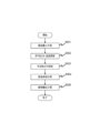
次に、上述の基板処理装置100の処理炉を用いて、半導体装置(デバイス)の製造工程の一工程として、例えば、基板上に形成されたシリコン含有膜としてのアモルファスシリコン膜の改質(結晶化)方法の一例について図3に示した処理フローに沿って説明する。以下の説明において、基板処理装置100を構成する各部の動作はコントローラ121により制御される。
次に、上述の基板処理装置100の処理炉を用いて、半導体装置(デバイス)の製造工程の一工程として、例えば、基板上に形成されたシリコン含有膜としてのアモルファスシリコン膜の改質(結晶化)方法の一例について図3に示した処理フローに沿って説明する。以下の説明において、基板処理装置100を構成する各部の動作はコントローラ121により制御される。
ここで、本明細書において「ウエハ」という言葉を用いた場合は、「ウエハ(プロダクトウエハ)そのもの」を意味する場合や、「ウエハとその表面に形成された所定の層や膜等との積層体(集合体)」を意味する場合、すなわち、表面に形成された所定の層や膜等を含めてウエハと称する場合、後述する「ターゲット基板(ターゲットウエハ)」または後述する「ダミー基板(ダミーウエハ)」もしくは「ターゲット基板(ターゲットウエハ)とダミー基板(ダミーウエハ)の両方」を意味する場合がある。また、本明細書において「ウエハの表面」という言葉を用いた場合は、上述した「ウエハ」の定義を用いた「ウエハそのものの表面(露出面)」を意味する場合や、「ウエハ上に形成された所定の層や膜等の表面、すなわち、積層体としてのウエハの最表面」を意味する場合がある。
従って、本明細書において「ウエハに対して所定のガスを供給する」と記載した場合は、上述した「ウエハ」の定義を用いた「ウエハそのものの表面(露出面)に対して所定のガスを供給する」ことを意味する場合や、「ウエハ上に形成されている層や膜等に対して、すなわち、積層体としてのウエハの最表面に対して所定のガスを供給する」ことを意味する場合がある。また、本明細書において「ウエハ上に所定の層(または膜)を形成する」と記載した場合は、「ウエハそのものの表面(露出面)上に所定の層(または膜)を形成する」ことを意味する場合や、「ウエハ上に形成されている層や膜等の上、すなわち、積層体としてのウエハの最表面の上に所定の層(または膜)を形成する」ことを意味する場合がある。
また、本明細書において「基板」という言葉を用いた場合も、「ウエハ」という言葉を用いた場合と同義である。
(基板搬入工程(S301))
図1に示されているように、所定枚数のウエハ200がボート217に移載されると、駆動機構267は、載置台210を上昇させることでボート217を反応管103内側の処理室201に搬入(ボートローディング)する(S301)。
図1に示されているように、所定枚数のウエハ200がボート217に移載されると、駆動機構267は、載置台210を上昇させることでボート217を反応管103内側の処理室201に搬入(ボートローディング)する(S301)。
(炉内圧力・温度調整工程(S302))
処理室201内へのボート217の搬入が完了したら、処理室201内が所定の圧力(例えば10~100Pa)となるよう処理室201内の雰囲気を排気する。具体的には、真空ポンプ246により排気しつつ、圧力センサ245により検出された圧力情報に基づいて圧力調整器244の弁開度をフィードバック制御し、処理室201内を所定の圧力とする。また、同時に予備加熱としてマイクロ波供給部を制御し、所定の温度まで加熱を行うように制御してもよい(S302)。
処理室201内へのボート217の搬入が完了したら、処理室201内が所定の圧力(例えば10~100Pa)となるよう処理室201内の雰囲気を排気する。具体的には、真空ポンプ246により排気しつつ、圧力センサ245により検出された圧力情報に基づいて圧力調整器244の弁開度をフィードバック制御し、処理室201内を所定の圧力とする。また、同時に予備加熱としてマイクロ波供給部を制御し、所定の温度まで加熱を行うように制御してもよい(S302)。
(不活性ガス供給工程(S303))
駆動機構267は、シャフト255を回転させ、載置台210上のボート217を介してウエハ200を回転させる。このとき、窒素ガス等の不活性ガスがガス供給管232を介してノズル105から供給される(S303)。処理室201内の圧力は0Pa以上200,000Pa以下の範囲となる所定の値であって、例えば101300Pa以上101566Pa以下となるように調整される。
駆動機構267は、シャフト255を回転させ、載置台210上のボート217を介してウエハ200を回転させる。このとき、窒素ガス等の不活性ガスがガス供給管232を介してノズル105から供給される(S303)。処理室201内の圧力は0Pa以上200,000Pa以下の範囲となる所定の値であって、例えば101300Pa以上101566Pa以下となるように調整される。
(基板処理工程(S304))
処理室201内を所定の圧力となるように維持すると、マイクロ波発振器655-1、655-2はウエハ200を100℃以上700℃以下の温度帯、好適には200℃以上600℃以下の温度帯となるように加熱し、さらに好適には、200℃以上400℃以下となるように加熱する。ウエハ200が100℃より低い温度で処理しようとした場合や、700℃よりも高い温度で処理しようとした場合、ウエハ200がマイクロ波を吸収し難くなってしまい、ウエハ200を効率的に加熱することができなくなってしまう。
処理室201内を所定の圧力となるように維持すると、マイクロ波発振器655-1、655-2はウエハ200を100℃以上700℃以下の温度帯、好適には200℃以上600℃以下の温度帯となるように加熱し、さらに好適には、200℃以上400℃以下となるように加熱する。ウエハ200が100℃より低い温度で処理しようとした場合や、700℃よりも高い温度で処理しようとした場合、ウエハ200がマイクロ波を吸収し難くなってしまい、ウエハ200を効率的に加熱することができなくなってしまう。
ウエハ200の温度は、石英サセプタ101aの表面温度を温度センサ263によって測定した値から、記憶装置121cまたは外部記憶装置122に予め記憶された温度変換データによって推測される。マイクロ波発振器655-1、655-2は、導波管654-1と654-2を介して電磁波導入ポート653-1と653-2からマイクロ波を処理室201内に供給する。処理室201内に供給されたマイクロ波はウエハ200に入射して効率的に吸収されるために、ウエハ200を極めて効果的に加熱することが可能となる。
マイクロ波発振器655を制御することでウエハ200を上述した所定の処理温度まで加熱すると、予め定められた時間、当該処理温度を維持する。このようにマイクロ波発振器655を制御することでマイクロ波ウエハ200の表面上に形成されたアモルファスシリコン膜の改質処理を行う。
ウエハ200を加熱する場合、マイクロ波発振器655-1、655-2は、マイクロ波を間欠的に供給しながらマイクロ波発振器655-1、655-2の出力を大きくするように制御されることが好ましい。すなわち、マイクロ波発振器からのマイクロ波供給を間欠的に供給するパルス制御と、マイクロ波発振器655-1、655-2の出力を線形的に制御するパワーリミット制御を組合せて行うようにすることが好ましい。
このようにウエハ200の昇温時にマイクロ波をパルス制御して供給することによって処理室201内に定在波が形成されてウエハ表面に集中して加熱される領域(マイクロ波集中領域、ホットスポット)が形成されたとしても、マイクロ波を供給しない時間(OFF時間)を設けることができる。マイクロ波を供給しないタイミングを設けることによって、マイクロ波集中領域に生じた熱がウエハ200の面内全体に伝達され、ウエハ200の面内温度を均一に維持することが可能となる。このようにウエハ200の面内で熱伝達が起きる期間を設けることによって、マイクロ波集中領域が集中して加熱されてしまうことを抑制することが可能となる。
したがって、マイクロ波をパルス制御して供給することによって、マイクロ波集中領域だけが集中して加熱され、マイクロ波集中領域とその他のウエハ面との温度差が大きくなることを抑制することができる。すなわち、マイクロ波集中領域のみが集中的かつ連続的に加熱されることによってウエハ200の表面に温度差が生じることを抑制でき、生じた温度差によってウエハ200が割れたり、反ったり、歪んだりするといったウエハ変形を抑制することが可能となる。
このようにウエハ200の昇温時にマイクロ波をパルス制御して供給することによって処理室201内に定在波が形成されてウエハ表面に集中して加熱される領域(マイクロ波集中領域、ホットスポット)が形成されたとしても、マイクロ波を供給しない時間(OFF時間)を設けることができる。マイクロ波を供給しないタイミングを設けることによって、マイクロ波集中領域に生じた熱がウエハ200の面内全体に伝達され、ウエハ200の面内温度を均一に維持することが可能となる。このようにウエハ200の面内で熱伝達が起きる期間を設けることによって、マイクロ波集中領域が集中して加熱されてしまうことを抑制することが可能となる。
したがって、マイクロ波をパルス制御して供給することによって、マイクロ波集中領域だけが集中して加熱され、マイクロ波集中領域とその他のウエハ面との温度差が大きくなることを抑制することができる。すなわち、マイクロ波集中領域のみが集中的かつ連続的に加熱されることによってウエハ200の表面に温度差が生じることを抑制でき、生じた温度差によってウエハ200が割れたり、反ったり、歪んだりするといったウエハ変形を抑制することが可能となる。
ここで、ウエハ200を効率よく加熱する、すなわち、ウエハ200がマイクロ波を効率よく吸収させるためには、ウエハ200のキャリア密度とキャリア温度依存性について検討する必要がある。図4に示すように、縦軸をキャリア密度(導電率に比例)、横軸を温度としたウエハ200のキャリア密度の温度依存性の一例を示した場合、温度によって、領域(A)、領域(B)、領域(C)に分けることができる。ウエハ200がシリコン(Si)基板である場合、例えば領域(A)と(B)を分ける温度は327℃、領域(B)と(C)とを分ける温度は-73℃である。図4から明らかであるように、領域(A)と(C)は温度上昇とともに、キャリア密度も大きく上昇するが、領域(B)は温度が上昇した場合であっても、キャリア密度は大きく上昇しない。
ウエハ200の単位時間当たりの発熱量はウエハ200のキャリア密度に比例するため、キャリア密度が変動するとそれに伴って発熱量も変化する。このため、キャリア密度の変化が大きい領域(A)で、マイクロ波加熱を行った場合、温度変化に応じてキャリア密度が増加する割合が大きいため、照射されるマイクロ波の電力が同じでも、ウエハ200の昇温速度が大きくなる。したがって、領域(A)において、マイクロ波による加熱が行われることが好ましい。
また、領域(A)は、上述したようにウエハ200の昇温速度が大きいため、マイクロ波が局所的に集中すると、集中した箇所が高温となりウエハ200の面内で部分的に温度差が大きくなり、熱膨張差でウエハ200が変形してしまう。このため、領域(A)の温度帯でマイクロ波による加熱を行いつつウエハ200を冷却することで、ウエハ200の面内温度差を小さくしてウエハ200が変形することを抑制しつつ、ウエハ200の改質処理速度を向上させることが可能となる。
マイクロ波による加熱を行いつつウエハ200を冷却するためには、例えば図5に示すようにマイクロ波発振器655のON/OFFに合わせて冷却ガスとしての不活性ガス(例えばN2ガスなど)の供給流量を増減するように制御するとよい。具体的には、図5に示すように、マイクロ波発振器655がONとなったタイミングにおける冷却ガスとしての不活性ガス(N2ガス)の流量が0.1slm以上10slm以下となるようにMFC241を制御し、マイクロ波発振器655がOFFとなったタイミングにおけるN2ガスの流量が0.1slm以上30slm以下となるようにMFC241を制御することで、ウエハ200を一定の温度帯に維持することができる。マイクロ波発振器655がONとなったタイミングで供給する冷却ガスの流量を0.1slm以下とした場合、マイクロ波を供給する際に処理室201内の圧力が下がり、プラズマ放電が生じる可能性がある。処理室201内でプラズマ放電が生じてしまうと、ウエハ200がプラズマ放電によるダメージを受ける可能性がある。同様に、マイクロ波発振器655がONとなったタイミングで供給する冷却ガスの流量を10slm以上とした場合、ウエハ200を加熱することができなくなってしまい、効率よく基板処理を行うことができなくなってしまう。また、マイクロ波発振器655がOFFとなったタイミングで供給する冷却ガスの流量を0.1slm以下とした場合、ウエハ200を効率よく冷却することができず、基板処理時間が長くなってしまう。同様に、マイクロ波発振器655がOFFとなったタイミングで供給する冷却ガスの流量を30slm以上とした場合、処理室201内の圧力が過加圧となってしまい、ウエハ200や処理装置が破損してしまう可能性も生じてしまう。このようにガス供給部とマイクロ波供給部とを制御することによって、ウエハ200の温度を最適な温度に維持することが可能となる。
また、ガス供給流量を増減するタイミングに合わせて処理室201内の圧力を増減するようにガス供給部と排気部を制御することとしてもよい。すなわち、マイクロ波発振器655がONとなっているタイミングにおいては、処理室201内の圧力は基板処理に適した所定の圧力となるように制御され、マイクロ波発振器655がOFFとなっているタイミングにおいては、処理室201内の圧力は特に制御しないようにする、すなわち、排気部(特に圧力調整部244)の制御をOFFにすることで、基板処理工程の制御を単純化することができる。
例えば、図5(A)に示すようにマイクロ波発振器655がONとなっているタイミングにおいては、MFC241を制御して冷却ガスを5slm供給するとともに、処理室201内の圧力が101300Pa(または101300Pa以上101566Pa以下の範囲)となるように圧力調整器244を制御する。また、マイクロ波発振器655がOFFとなっているタイミングにおいては、MFC241を制御して冷却ガスを制御して冷却ガスを15slm供給し、圧力調整部244をOFFとする為、処理室201内の圧力は冷却ガスを供給した分だけ昇圧された略101966Pa(または、101433Pa以上102232Pa以下の範囲)となるようにマイクロ波供給部とガス供給部を制御する。このように処理室201内の圧力について積極的に制御しない場合であっても、冷却ガスの供給流量を制御することによって、処理室201内を過加圧などの不具合が生じる圧力以下に抑えることが可能であるため、圧力について詳細な制御を不要とする処理を行う場合には有効である。
また、図5(B)に示すように、温度センサ263によって測定した温度、または、上述した予め記憶された温度変換データによって推測された温度に応じてガス供給部を制御するようにしてもよい。すなわち、マイクロ波発振器655を常時ONとし、加熱されたウエハ200の温度が所定の目標温度(閾値となる温度、例えば図5(B)では400℃)よりも高い温度となったタイミングでガス供給部、具体的にはMFC241の開度を大きくして冷却ガスの流量を増加させ、ウエハ200を冷却する。逆にウエハ200の温度が所定の目標温度よりも低い温度となったタイミングでMFC241の開度を小さくして冷却ガスの流量を低下させ、ウエハ200を加熱する。このようにマイクロ波供給部とガス供給部を制御することによって、ガス供給部のみを詳細に制御することで足りるため、ウエハ200の温度制御を単純化することが可能となる。
さらに、マイクロ波発振器655-1、655-2によってマイクロ波を供給する時間(ON時間)と、マイクロ波を供給しない時間(OFF時間)の間隔、すなわちパルス幅は、例えば1×10⁻⁴sec間隔で制御できるようにすることが好ましい。このように構成することで、ウエハ昇温時とウエハ処理時の両方において正確な温度制御を可能とする。
なお、ウエハ昇温時とウエハ処理時で異なるパルス幅になるよう制御してもよい。このように構成することによって、ウエハ200の表面におけるマイクロ波集中領域とそれ以外の面の温度差が大きくなり易い(マイクロ波集中領域以外の領域が加熱されていない)ウエハ昇温時にはパルス幅を小さくすることで、面内温度均一性を向上させることが可能となる。同様に、ウエハ200の表面におけるマイクロ波集中領域とそれ以外の面の温度差が大きくなり難い(マイクロ波集中領域以外の領域がある程度加熱されている)ウエハ処理時にはパルス幅を大きくすることで、ウエハ表面にマイクロ波を十分に照射することが可能となり、十分なウエハ処理を行うことが可能となる。
また、パルス幅のON時間とOFF時間との時間間隔をそれぞれ異なるように制御してもよい。
以上のようにウエハ200を加熱処理することによってウエハ200表面上に形成されているアモルファスシリコン膜がポリシリコン膜へと改質(結晶化)されることとなる。すなわち、ウエハ200を均一に改質することが可能となる(S304)。
なお、ウエハ昇温時とウエハ処理時で異なるパルス幅になるよう制御してもよい。このように構成することによって、ウエハ200の表面におけるマイクロ波集中領域とそれ以外の面の温度差が大きくなり易い(マイクロ波集中領域以外の領域が加熱されていない)ウエハ昇温時にはパルス幅を小さくすることで、面内温度均一性を向上させることが可能となる。同様に、ウエハ200の表面におけるマイクロ波集中領域とそれ以外の面の温度差が大きくなり難い(マイクロ波集中領域以外の領域がある程度加熱されている)ウエハ処理時にはパルス幅を大きくすることで、ウエハ表面にマイクロ波を十分に照射することが可能となり、十分なウエハ処理を行うことが可能となる。
また、パルス幅のON時間とOFF時間との時間間隔をそれぞれ異なるように制御してもよい。
以上のようにウエハ200を加熱処理することによってウエハ200表面上に形成されているアモルファスシリコン膜がポリシリコン膜へと改質(結晶化)されることとなる。すなわち、ウエハ200を均一に改質することが可能となる(S304)。
予め設定された処理時間が経過すると、ボート217の回転、ガスの供給、マイクロ波の供給および排気管の排気が停止する。
基板処理工程の終了後、N2ガスなどの不活性ガスを供給し、処理室201内の圧力を大気圧に復帰する。
(基板搬出工程(S305))
処理室201内の圧力を大気圧復帰させた後に、駆動機構267は載置台210を下降させることにより、炉口を開口するとともに、ボート217を搬送空間203に搬出(ボートアンローディング)する。その後ボートに載置されているウエハ200を搬送空間203の外部に位置する搬送室に搬出する(S305)。
以上の動作が繰り返されることにより、ウエハ200が改質処理されることとなる。
処理室201内の圧力を大気圧復帰させた後に、駆動機構267は載置台210を下降させることにより、炉口を開口するとともに、ボート217を搬送空間203に搬出(ボートアンローディング)する。その後ボートに載置されているウエハ200を搬送空間203の外部に位置する搬送室に搬出する(S305)。
以上の動作が繰り返されることにより、ウエハ200が改質処理されることとなる。
(3)本実施形態による効果
本実施形態によれば以下に示す1つまたは複数の効果を奏する。
本実施形態によれば以下に示す1つまたは複数の効果を奏する。
(a)ウエハの加熱を行うとともに冷却ガスとしての不活性ガスを供給することによって、ウエハの温度を所定の温度に維持することが可能となり、効率的にウエハを昇温することが可能となる。
(b)効率的にウエハを昇温することが可能となるため、基板処理時間を短くすることが可能となる。
(c)マイクロ波発振器のON/OFFに連動して不活性ガスの流量を増減させることで、効率的にウエハ温度を維持することが可能となる。
(d)ウエハを冷却するタイミングでは処理室内の圧力制御を行わないようにすることで、圧力制御を単純化することが可能となる。
(4)第1の実施形態の変形例
本実施形態における基板処理装置は、上述の態様に限定されず、以下に示す変形例のように変更することができる。
本実施形態における基板処理装置は、上述の態様に限定されず、以下に示す変形例のように変更することができる。
(変形例1)
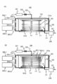
図6(A)に示すように、第1の実施形態における変形例1は、ボート217がウエハ200を複数多段に保持可能に構成している。具体的には、ボート217に保持された断熱板101aと101bの間に複数枚のウエハ200を所定の間隔で水平多段に保持するように構成し、上述した基板処理工程の順番で保持された複数枚のウエハ200が均等に処理される。このように構成することによって、一度の処理で複数枚のウエハ200が処理可能となり、基板処理のスループットを向上させることが可能となる。
ここで、図6(A)では、複数枚のウエハ200は断熱板101a、101bの間に挟まれるように保持されているが、これに限らず、複数のウエハ200それぞれを複数の断熱板101a、101bで挟み込んで保持するように構成してもよい。この場合、断熱板101aと101bも複数枚設けられることとなる。このように構成することによって、第1の実施形態と比較してウエハ200をより早く加熱することが可能となるばかりでなく、ウエハ面内の温度均一性を向上させることが可能となる。
図6(A)に示すように、第1の実施形態における変形例1は、ボート217がウエハ200を複数多段に保持可能に構成している。具体的には、ボート217に保持された断熱板101aと101bの間に複数枚のウエハ200を所定の間隔で水平多段に保持するように構成し、上述した基板処理工程の順番で保持された複数枚のウエハ200が均等に処理される。このように構成することによって、一度の処理で複数枚のウエハ200が処理可能となり、基板処理のスループットを向上させることが可能となる。
ここで、図6(A)では、複数枚のウエハ200は断熱板101a、101bの間に挟まれるように保持されているが、これに限らず、複数のウエハ200それぞれを複数の断熱板101a、101bで挟み込んで保持するように構成してもよい。この場合、断熱板101aと101bも複数枚設けられることとなる。このように構成することによって、第1の実施形態と比較してウエハ200をより早く加熱することが可能となるばかりでなく、ウエハ面内の温度均一性を向上させることが可能となる。
(変形例2)
図6(B)に示すように、第1の実施形態における変形例2は、ボート217を挟んでノズル105に対向する位置に排気用の排気ノズル601を設置するように構成している。ガス供給ノズル側に面する排気ノズル601の側面には処理室201内の雰囲気を排気するための排気口が設けられ、排気ノズル601の下流側には排気管231が接続されている。このように構成することによって、処理室201内の圧力が大気圧または微加圧の状態であっても、ウエハ側面から水平に冷却ガスを供給し、水平なガス流れを形成することが可能となり、ウエハ200を均一に冷却することが可能となる。したがって、ウエハ面内の温度均一性を向上させることが可能となる。
図6(B)に示すように、第1の実施形態における変形例2は、ボート217を挟んでノズル105に対向する位置に排気用の排気ノズル601を設置するように構成している。ガス供給ノズル側に面する排気ノズル601の側面には処理室201内の雰囲気を排気するための排気口が設けられ、排気ノズル601の下流側には排気管231が接続されている。このように構成することによって、処理室201内の圧力が大気圧または微加圧の状態であっても、ウエハ側面から水平に冷却ガスを供給し、水平なガス流れを形成することが可能となり、ウエハ200を均一に冷却することが可能となる。したがって、ウエハ面内の温度均一性を向上させることが可能となる。
<本発明の第2の実施形態>
次に本発明の第2の実施形態を図7を用いて説明する。
次に本発明の第2の実施形態を図7を用いて説明する。
第2の実施形態において、本発明に係る基板処理装置が第1の実施形態と異なる点は、図7に示すように、ガス供給部がガス供給ノズルを設けずにキャップフランジ104を貫通するように設けられ、ウエハ上方より冷却ガスが供給される点と、冷却ガスがボート217の上側端板(天板とも称する)に直接噴射されることを抑制するガス整流部700を有する点である。
なお、本実施形態において、第1の実施形態と同一の機能を有する構成要素には、同一の参照番号を付し、説明を省略する。
なお、本実施形態において、第1の実施形態と同一の機能を有する構成要素には、同一の参照番号を付し、説明を省略する。
図7に示すように、本実施形態では、処理室201の上方に設けられたキャップフランジ104を貫通するようにガス供給管232を設置し、処理室201の上方に設けられたガス供給口703から冷却ガスを供給している。処理室201の上方に設けられたガス供給口703に対向する位置には、冷却ガスがボート217に直接当たることでボート217の温度が局所的に冷却され、ウエハ200の面内温度均一性に影響が生じることを避けるため、ガスの流れを整流するガス整流板701と、ガス整流板701をキャップフランジ104に固定するための固定部702によって構成されるガス整流部700が設けられている。
ガス整流部700は、ガス供給口703に対向する位置に設けられることで、キャップフランジ104の略中心部から供給される冷却ガスがガス整流板701の外周側から流れるように冷却ガス流れの方向を変えるために設けられており、ガス整流板701の直径を変化させることで所望する位置に冷却ガスが流れるように制御することが可能となる。例えば、ガス整流板701はボート217の天板外径よりも大きな直径を有する円盤形状に形成され、ボート217の外周に冷却ガスが流れるように構成される。このように構成することによって、装置構造を複雑化することなく第1の実施形態と比べてガス供給部の制御を単純化することが可能となる。また、ウエハ外周から均等に冷却することが可能となるため、ウエハ200の面内温度均一性を向上させることが可能となる。
(5)本実施形態による効果
本実施形態によれば、第1の実施形態と同様の効果を得られるだけでなく、以下に示す1つまたは複数の効果を奏する。
本実施形態によれば、第1の実施形態と同様の効果を得られるだけでなく、以下に示す1つまたは複数の効果を奏する。
(e)冷却ガスを上方から供給するとともにガス整流部を設けることによって、ウエハ外周から均等に冷却することが可能となる。
(f)ガス整流部を設けることによって、装置構造を複雑化することなく、ガス供給部の制御を単純化することが可能となる。
(6)第2の実施形態の変形例
本実施形態における基板処理装置は、上述の態様に限定されず、以下に示す変形例のように変更することができる。
本実施形態における基板処理装置は、上述の態様に限定されず、以下に示す変形例のように変更することができる。
(変形例1)
図8(A)に示すように、第2の実施形態における変形例1は、ボート217の高さ方向を高くし、ボート217の天板部をガス整流部として機能させることで冷却ガスがウエハ200の面内温度均一性に影響を与えることを抑制するように構成している。このように構成することによって、新たな部品を処理室内に設置する必要が無くなるため、コスト低減となるだけでなく、パーティクルの発生を抑制することが可能となる。
(変形例2)
図8(B)に示すように、第2の実施形態における変形例2は、変形例1と同様にボート217の高さ方向を高くし、ボート217の天板部をガス整流部として機能させるとともに、断熱板101aの上方に位置するように断熱板801-1、801-2をボート217に保持させる構成している。このように構成することによって、変形例1よりもさらに高い断熱性を有することが可能となり、ボート217からの伝導熱によってウエハ200の処理に影響を与えることをより抑制することが可能となる。ここで、断熱板801-1、801-2は、断熱板101a、101bと同一のものであってもよいし、異なる材質、断熱性を有するものであってもよい。
図8(A)に示すように、第2の実施形態における変形例1は、ボート217の高さ方向を高くし、ボート217の天板部をガス整流部として機能させることで冷却ガスがウエハ200の面内温度均一性に影響を与えることを抑制するように構成している。このように構成することによって、新たな部品を処理室内に設置する必要が無くなるため、コスト低減となるだけでなく、パーティクルの発生を抑制することが可能となる。
(変形例2)
図8(B)に示すように、第2の実施形態における変形例2は、変形例1と同様にボート217の高さ方向を高くし、ボート217の天板部をガス整流部として機能させるとともに、断熱板101aの上方に位置するように断熱板801-1、801-2をボート217に保持させる構成している。このように構成することによって、変形例1よりもさらに高い断熱性を有することが可能となり、ボート217からの伝導熱によってウエハ200の処理に影響を与えることをより抑制することが可能となる。ここで、断熱板801-1、801-2は、断熱板101a、101bと同一のものであってもよいし、異なる材質、断熱性を有するものであってもよい。
<本発明の第3の実施形態>
次に本発明の第3の実施形態を図9を用いて説明する。
次に本発明の第3の実施形態を図9を用いて説明する。
第3の実施形態において、本発明に係る基板処理装置が第1の実施形態および第2の実施形態と異なる点は、図9に示すように、処理室201上方にシャワーヘッドを設けて冷却ガスを供給する点である。
なお、本実施形態において、第1の実施形態と同一の機能を有する構成要素には、同一の参照番号を付し、説明を省略する。
なお、本実施形態において、第1の実施形態と同一の機能を有する構成要素には、同一の参照番号を付し、説明を省略する。
図9に示すように、本実施形態では、ガス供給管232の下流端にシャワーヘッド901を設置し、シャワーヘッド901の分散板901aから冷却ガスを分散して処理室201上方から下方に向けてガス流れを形成する。
シャワーヘッド901は、ガス供給管232から供給された冷却ガスを分散板901aに設けた複数のガス供給口901bを介して供給する。また、シャワーヘッド901は、分散板901に設けられた複数のガス供給口901bの設置位置や設置数、ガス供給口の供給面積を変化させることで所望のガス流れを形成することを可能としている。例えば、最外側に設けられたガス供給口901をボート217の天板外径よりも外側に設けるように形成することで、ボート217の外周側にも冷却ガスが流れる様に構成される。このように構成することによって、ボート217の天板に直接冷却ガスが供給される場合であっても、冷却ガスを分散して供給することが可能となるため、ウエハ200の改質処理に影響を与えるほどの冷却が行われることを抑制することができる。
(7)本実施形態による効果
本実施形態によれば、第1の実施形態または第2の実施形態と同様の効果を得られるだけでなく、以下に示す1つまたは複数の効果を奏する。
本実施形態によれば、第1の実施形態または第2の実施形態と同様の効果を得られるだけでなく、以下に示す1つまたは複数の効果を奏する。
(g)冷却ガスをシャワーヘッドを介して供給することによって、処理室内に供給する冷却ガスを分散して供給することが可能となり、ウエハ200の処理時に影響を与えるほど冷却されてしまうことを抑制することが可能となる。
以上、本発明を実施形態に沿って説明してきたが、上述の各実施形態や各変形例等は、適宜組み合わせて用いることができ、その効果も得ることができる。
また、例えば、上述の各実施形態では、シリコンを主成分とする膜として、アモルファスシリコン膜をポリシリコン膜に改質する処理について記載したが、これに限らず、酸素(O)、窒素(N)、炭素(C)、水素(H)のうち、少なくとも1つ以上を含むガスを供給させて、ウエハ200の表面に形成された膜を改質しても良い。例えば、ウエハ200に、高誘電体膜としてのハフニウム酸化膜(HfxOy膜)が形成されている場合に、酸素を含むガスを供給しながらマイクロ波を供給して加熱させることによって、ハフニウム酸化膜中の欠損した酸素を補充し、高誘電体膜の特性を向上させたり、窒素ガス(N2ガス)を供給しながらマイクロ波を供給して加熱させることによって、ハフニウム酸化膜中の未結晶化部分を結晶化し、高誘電体膜の特性を向上させたりすることができる。
なお、ここでは、ハフニウム酸化膜について示したが、これに限らず、Al、Ti、Zr、Ta、Nb、La、Ce、Y、Ba、Sr、Ca、Pb、Mo、W等の少なくともいずれかを含む金属元素を含む酸化膜、すなわち、金属系酸化膜を形成する場合においても、好適に適用可能である。すなわち、上述の成膜シーケンスは、ウエハ200上に、Ti膜、TiN膜、TiOCN膜、TiOC膜、TiON膜、TiO膜、ZrN膜、ZrOCN膜、ZrOC膜、ZrON膜、ZrO膜、HfOCN膜、HfOC膜、HfON膜、HfO膜、TaOCN膜、TaOC膜、TaON膜、TaO膜、NbOCN膜、NbOC膜、NbON膜、NbO膜、AlOCN膜、AlOC膜、AlON膜、AlO膜、MoOCN膜、MoOC膜、MoON膜、MoO膜、W膜、WOCN膜、WOC膜、WON膜、WO膜を形成する場合にも、好適に適用することが可能となる。
なお、ここでは、ハフニウム酸化膜について示したが、これに限らず、Al、Ti、Zr、Ta、Nb、La、Ce、Y、Ba、Sr、Ca、Pb、Mo、W等の少なくともいずれかを含む金属元素を含む酸化膜、すなわち、金属系酸化膜を形成する場合においても、好適に適用可能である。すなわち、上述の成膜シーケンスは、ウエハ200上に、Ti膜、TiN膜、TiOCN膜、TiOC膜、TiON膜、TiO膜、ZrN膜、ZrOCN膜、ZrOC膜、ZrON膜、ZrO膜、HfOCN膜、HfOC膜、HfON膜、HfO膜、TaOCN膜、TaOC膜、TaON膜、TaO膜、NbOCN膜、NbOC膜、NbON膜、NbO膜、AlOCN膜、AlOC膜、AlON膜、AlO膜、MoOCN膜、MoOC膜、MoON膜、MoO膜、W膜、WOCN膜、WOC膜、WON膜、WO膜を形成する場合にも、好適に適用することが可能となる。
また、高誘電体膜に限らず、不純物がドーピングされたシリコンを主成分とする膜を加熱させるようにしてもよい。シリコンを主成分とする膜としては、SiN膜、SiO膜、SiOC膜、SiOCN膜、SiON膜等のSi系酸化膜、Epi-Si膜、Epi-SiGe膜等がある。不純物としては、例えば、B、C、N、Al、P、Ga、Asなどの少なくとも1つ以上を含む。なお、上述したシリコンを主成分とする膜や金属酸化膜の他、Epi-Ge膜や、3-5族元素を用いて形成する膜を加熱するようにしてもよい。
また、メタクリル酸メチル樹脂(Polymethyl methacrylate:PMMA)、エポキシ樹脂、ノボラック樹脂、ポリビニルフェニール樹脂などの少なくともいずれかをベースとするレジスト膜であってもよい。
また、上述では、半導体装置の製造工程の一工程について記したが、これに限らず、液晶パネルの製造工程のパターニング処理、太陽電池の製造工程のパターニング処理や、パワーデバイスの製造工程のパターニング処理などの、基板を処理する技術にも適用可能である。
以上述べたように、本発明は、均一な基板処理を行うことが可能となる技術を提供することができる。
100・・・基板処理装置、
101a、101b・・・断熱板(石英板、Si板)
102・・・ケース(キャビティ)、
103・・・反応管、
105・・・ノズル、
121・・・コントローラ(制御部)、
200・・・ウエハ(基板)、
201・・・処理室、
217・・・ボート(基板保持具)、
655・・・マイクロ波発振器(加熱装置)。
101a、101b・・・断熱板(石英板、Si板)
102・・・ケース(キャビティ)、
103・・・反応管、
105・・・ノズル、
121・・・コントローラ(制御部)、
200・・・ウエハ(基板)、
201・・・処理室、
217・・・ボート(基板保持具)、
655・・・マイクロ波発振器(加熱装置)。
Claims (10)
- 基板と断熱板を保持する基板保持具が搬入されて前記基板を処理する処理室と、
前記処理室内にマイクロ波を供給するマイクロ波供給部を有する加熱装置と、
前記処理室内に冷却ガスを供給するガス供給部と、
前記加熱装置によって前記基板を加熱する加熱時に前記ガス供給部から冷却ガスを供給することで前記基板を所定の温度に維持するように前記加熱装置と前記ガス供給部とを制御するよう構成される制御部と、
を有する基板処理装置。 - 前記制御部は、前記基板の加熱を間欠的に行うように前記加熱装置を制御するよう構成され、
さらに、前記加熱装置による加熱を行うタイミングでは前記冷却ガスの供給流量を少なくし、前記加熱装置による加熱を停止しているタイミングで前記冷却ガスの供給流量を増加させるように前記ガス供給部を制御するよう構成される請求項1に記載の基板処理装置。 - 前記制御部は、前記加熱装置による加熱を行うタイミングで供給する前記冷却ガスの流量を0.1slm以上10slm以下とし、前記加熱装置による加熱を停止しているタイミングで供給する前記冷却ガスの流量を0.1slm以上30slm以下とするように前記ガス供給部を制御するよう構成される請求項2に記載の基板処理装置。
- 前記制御部は、前記基板が100℃以上700℃以下の温度で処理されるように前記加熱装置と前記冷却装置を制御するよう構成される請求項1に記載の基板処理装置。
- 前記ガス供給部に対向する位置に設けられ、前記処理室内の雰囲気を排気する排気ノズルをさらに有する請求項1に記載の基板処理装置。
- 前記ガス供給部は、前記処理室の天井面から前記冷却ガスを供給するように設置され、
前記ガス供給部に対向する位置であって前記基板保持具よりも上方に前記冷却ガスを整流するガス整流部をさらに有する請求項1に記載の基板処理装置。 - 前記ガス供給部は、前記処理室の天井部に前記冷却ガスを分散して供給するシャワーヘッドを有する請求項1に記載の基板処理装置。
- 前記断熱板は前記基板を挟み込むように上下に配置されて前記基板保持具に保持される請求項1に記載の基板処理装置。
- 基板と断熱板を保持する基板保持具が搬入されて前記基板を処理する処理室と、前記処理室内にマイクロ波を供給するマイクロ波供給部を有する加熱装置と、前記処理室内に冷却ガスを供給するガス供給部と、前記加熱装置によって前記基板を加熱する加熱時に前記ガス供給部から冷却ガスを供給することで前記基板を所定の温度に維持するように前記加熱装置と前記ガス供給部とを制御する制御部と、を有する基板処理装置の前記処理室内に前記基板を搬入する工程と、
前記基板を加熱して所定の処理を行う工程と、
前記基板を前記処理室から搬出する工程と、
を有する半導体装置の製造方法。 - 基板と断熱板を保持する基板保持具が搬入されて前記基板を処理する処理室と、前記処理室内にマイクロ波を供給するマイクロ波供給部を有する加熱装置と、前記処理室内に冷却ガスを供給するガス供給部と、前記加熱装置によって前記基板を加熱する加熱時に前記ガス供給部から冷却ガスを供給することで前記基板を所定の温度に維持するように前記加熱装置と前記ガス供給部とを制御する制御部と、を有する基板処理装置の前記処理室内に前記基板を搬入する手順と、
前記基板を加熱して所定の処理を行う手順と、
前記基板を前記処理室から搬出する手順と、
をコンピュータによって基板処理装置に実行させるプログラムを記録したコンピュータ読み取り可能な記録媒体。
Priority Applications (2)
| Application Number | Priority Date | Filing Date | Title |
|---|---|---|---|
| JP2018502912A JP6731471B2 (ja) | 2016-03-01 | 2016-03-01 | 基板処理装置、半導体装置の製造方法および記録媒体 |
| PCT/JP2016/056275 WO2017149663A1 (ja) | 2016-03-01 | 2016-03-01 | 基板処理装置、半導体装置の製造方法および記録媒体 |
Applications Claiming Priority (1)
| Application Number | Priority Date | Filing Date | Title |
|---|---|---|---|
| PCT/JP2016/056275 WO2017149663A1 (ja) | 2016-03-01 | 2016-03-01 | 基板処理装置、半導体装置の製造方法および記録媒体 |
Publications (1)
| Publication Number | Publication Date |
|---|---|
| WO2017149663A1 true WO2017149663A1 (ja) | 2017-09-08 |
Family
ID=59743578
Family Applications (1)
| Application Number | Title | Priority Date | Filing Date |
|---|---|---|---|
| PCT/JP2016/056275 Ceased WO2017149663A1 (ja) | 2016-03-01 | 2016-03-01 | 基板処理装置、半導体装置の製造方法および記録媒体 |
Country Status (2)
| Country | Link |
|---|---|
| JP (1) | JP6731471B2 (ja) |
| WO (1) | WO2017149663A1 (ja) |
Cited By (12)
| Publication number | Priority date | Publication date | Assignee | Title |
|---|---|---|---|---|
| JPWO2019186655A1 (ja) * | 2018-03-26 | 2021-02-12 | 株式会社Kokusai Electric | 基板処理装置、半導体装置の製造方法およびプログラム |
| JP2021019143A (ja) * | 2019-07-23 | 2021-02-15 | 株式会社Kokusai Electric | 基板処理装置、半導体装置の製造方法およびプログラム |
| JPWO2019180966A1 (ja) * | 2018-03-23 | 2021-02-18 | 株式会社Kokusai Electric | 基板処理装置、半導体装置の製造方法及びプログラム |
| US11239098B2 (en) | 2018-03-22 | 2022-02-01 | Kokusai Electric Corporation | Substrate processing apparatus, method of manufacturing semiconductor device, and recording medium |
| KR20220111666A (ko) | 2021-02-02 | 2022-08-09 | 가부시키가이샤 코쿠사이 엘렉트릭 | 기판 처리 장치, 기판 보유 지지 장치, 반도체 장치의 제조 방법 및 프로그램 |
| CN115838920A (zh) * | 2021-09-21 | 2023-03-24 | 铠侠股份有限公司 | 半导体制造装置、半导体装置的制造方法以及成膜方法 |
| JP2023092250A (ja) * | 2021-12-21 | 2023-07-03 | キヤノン株式会社 | 基板処理装置および基板処理方法 |
| JP2023141761A (ja) * | 2022-03-24 | 2023-10-05 | 株式会社Kokusai Electric | 半導体装置の製造方法、基板処理方法、プログラム、及び基板処理装置 |
| JP2023143716A (ja) * | 2022-03-24 | 2023-10-06 | 株式会社Kokusai Electric | 基板処理装置、半導体装置の製造方法およびプログラム |
| KR20230140485A (ko) * | 2022-03-24 | 2023-10-06 | 가부시키가이샤 코쿠사이 엘렉트릭 | 기판 처리 장치, 반도체 장치의 제조 방법 및 프로그램 |
| JP2024044808A (ja) * | 2022-09-21 | 2024-04-02 | 株式会社Kokusai Electric | 基板処理装置、半導体装置の製造方法およびプログラム |
| WO2025158724A1 (ja) * | 2024-01-24 | 2025-07-31 | 株式会社Kokusai Electric | 基板処理方法、半導体装置の製造方法、基板処理装置、およびプログラム |
Citations (8)
| Publication number | Priority date | Publication date | Assignee | Title |
|---|---|---|---|---|
| JPS6143417A (ja) * | 1984-08-08 | 1986-03-03 | Hitachi Ltd | 加熱処理方法とそれを用いた加熱装置 |
| JP2006032386A (ja) * | 2004-07-12 | 2006-02-02 | Hitachi Kokusai Electric Inc | 熱処理装置 |
| JP2010080555A (ja) * | 2008-09-24 | 2010-04-08 | Hitachi Kokusai Electric Inc | 基板処理装置 |
| JP2012191158A (ja) * | 2011-02-23 | 2012-10-04 | Tokyo Electron Ltd | マイクロ波照射装置 |
| JP2013152919A (ja) * | 2011-12-28 | 2013-08-08 | Tokyo Electron Ltd | マイクロ波加熱処理装置および処理方法 |
| JP2014033014A (ja) * | 2012-08-01 | 2014-02-20 | Tokyo Electron Ltd | マイクロ波照射装置 |
| JP2014033003A (ja) * | 2012-08-01 | 2014-02-20 | Tokyo Electron Ltd | 被処理体の処理方法 |
| JP2015103726A (ja) * | 2013-11-27 | 2015-06-04 | 東京エレクトロン株式会社 | マイクロ波加熱処理装置及びマイクロ波加熱処理方法 |
Family Cites Families (2)
| Publication number | Priority date | Publication date | Assignee | Title |
|---|---|---|---|---|
| JPH09260300A (ja) * | 1996-03-21 | 1997-10-03 | Kokusai Electric Co Ltd | 半導体製造装置 |
| JP2009302177A (ja) * | 2008-06-11 | 2009-12-24 | Hitachi Kokusai Electric Inc | 基板処理装置 |
-
2016
- 2016-03-01 WO PCT/JP2016/056275 patent/WO2017149663A1/ja not_active Ceased
- 2016-03-01 JP JP2018502912A patent/JP6731471B2/ja active Active
Patent Citations (8)
| Publication number | Priority date | Publication date | Assignee | Title |
|---|---|---|---|---|
| JPS6143417A (ja) * | 1984-08-08 | 1986-03-03 | Hitachi Ltd | 加熱処理方法とそれを用いた加熱装置 |
| JP2006032386A (ja) * | 2004-07-12 | 2006-02-02 | Hitachi Kokusai Electric Inc | 熱処理装置 |
| JP2010080555A (ja) * | 2008-09-24 | 2010-04-08 | Hitachi Kokusai Electric Inc | 基板処理装置 |
| JP2012191158A (ja) * | 2011-02-23 | 2012-10-04 | Tokyo Electron Ltd | マイクロ波照射装置 |
| JP2013152919A (ja) * | 2011-12-28 | 2013-08-08 | Tokyo Electron Ltd | マイクロ波加熱処理装置および処理方法 |
| JP2014033014A (ja) * | 2012-08-01 | 2014-02-20 | Tokyo Electron Ltd | マイクロ波照射装置 |
| JP2014033003A (ja) * | 2012-08-01 | 2014-02-20 | Tokyo Electron Ltd | 被処理体の処理方法 |
| JP2015103726A (ja) * | 2013-11-27 | 2015-06-04 | 東京エレクトロン株式会社 | マイクロ波加熱処理装置及びマイクロ波加熱処理方法 |
Cited By (20)
| Publication number | Priority date | Publication date | Assignee | Title |
|---|---|---|---|---|
| US11239098B2 (en) | 2018-03-22 | 2022-02-01 | Kokusai Electric Corporation | Substrate processing apparatus, method of manufacturing semiconductor device, and recording medium |
| JPWO2019180966A1 (ja) * | 2018-03-23 | 2021-02-18 | 株式会社Kokusai Electric | 基板処理装置、半導体装置の製造方法及びプログラム |
| JP7079317B2 (ja) | 2018-03-23 | 2022-06-01 | 株式会社Kokusai Electric | 基板処理装置、半導体装置の製造方法及びプログラム |
| JP7033651B2 (ja) | 2018-03-26 | 2022-03-10 | 株式会社Kokusai Electric | 基板処理装置、半導体装置の製造方法、プログラム、および、基板処理方法 |
| JPWO2019186655A1 (ja) * | 2018-03-26 | 2021-02-12 | 株式会社Kokusai Electric | 基板処理装置、半導体装置の製造方法およびプログラム |
| JP2021019143A (ja) * | 2019-07-23 | 2021-02-15 | 株式会社Kokusai Electric | 基板処理装置、半導体装置の製造方法およびプログラム |
| US12387969B2 (en) | 2021-02-02 | 2025-08-12 | Kokusai Electric Corporation | Substrate processing apparatus, substrate holding apparatus, and method of manufacturing semiconductor device |
| KR20220111666A (ko) | 2021-02-02 | 2022-08-09 | 가부시키가이샤 코쿠사이 엘렉트릭 | 기판 처리 장치, 기판 보유 지지 장치, 반도체 장치의 제조 방법 및 프로그램 |
| CN115838920A (zh) * | 2021-09-21 | 2023-03-24 | 铠侠股份有限公司 | 半导体制造装置、半导体装置的制造方法以及成膜方法 |
| JP2023092250A (ja) * | 2021-12-21 | 2023-07-03 | キヤノン株式会社 | 基板処理装置および基板処理方法 |
| JP7737303B2 (ja) | 2021-12-21 | 2025-09-10 | キヤノン株式会社 | 基板処理装置および基板処理方法 |
| JP2023143716A (ja) * | 2022-03-24 | 2023-10-06 | 株式会社Kokusai Electric | 基板処理装置、半導体装置の製造方法およびプログラム |
| JP7534458B2 (ja) | 2022-03-24 | 2024-08-14 | 株式会社Kokusai Electric | 基板処理装置、半導体装置の製造方法およびプログラム |
| JP7571073B2 (ja) | 2022-03-24 | 2024-10-22 | 株式会社Kokusai Electric | 半導体装置の製造方法、基板処理方法、プログラム、及び基板処理装置 |
| KR102822702B1 (ko) * | 2022-03-24 | 2025-06-18 | 가부시키가이샤 코쿠사이 엘렉트릭 | 기판 처리 장치, 반도체 장치의 제조 방법 및 프로그램 |
| KR20230140485A (ko) * | 2022-03-24 | 2023-10-06 | 가부시키가이샤 코쿠사이 엘렉트릭 | 기판 처리 장치, 반도체 장치의 제조 방법 및 프로그램 |
| JP2023141761A (ja) * | 2022-03-24 | 2023-10-05 | 株式会社Kokusai Electric | 半導体装置の製造方法、基板処理方法、プログラム、及び基板処理装置 |
| JP2024044808A (ja) * | 2022-09-21 | 2024-04-02 | 株式会社Kokusai Electric | 基板処理装置、半導体装置の製造方法およびプログラム |
| JP7719759B2 (ja) | 2022-09-21 | 2025-08-06 | 株式会社Kokusai Electric | 基板処理装置、半導体装置の製造方法、基板処理方法およびプログラム |
| WO2025158724A1 (ja) * | 2024-01-24 | 2025-07-31 | 株式会社Kokusai Electric | 基板処理方法、半導体装置の製造方法、基板処理装置、およびプログラム |
Also Published As
| Publication number | Publication date |
|---|---|
| JPWO2017149663A1 (ja) | 2018-12-20 |
| JP6731471B2 (ja) | 2020-07-29 |
Similar Documents
| Publication | Publication Date | Title |
|---|---|---|
| JP6731471B2 (ja) | 基板処理装置、半導体装置の製造方法および記録媒体 | |
| JP6454425B2 (ja) | 半導体装置の製造方法、基板処理装置およびプログラム | |
| US11265977B2 (en) | Substrate processing apparatus, method of manufacturing semiconductor device, and recording medium | |
| US11239098B2 (en) | Substrate processing apparatus, method of manufacturing semiconductor device, and recording medium | |
| US20200013646A1 (en) | Substrate processing apparatus, method of manufacturing semiconductor device, and recording medium | |
| TWI808537B (zh) | 基板處理裝置,基板保持裝置,半導體裝置的製造方法及程式 | |
| JPWO2019167235A1 (ja) | 基板処理装置、半導体装置の製造方法およびプログラム | |
| US20210407865A1 (en) | Method of Manufacturing Semiconductor Device, Substrate Processing Apparatus and Non-transitory Computer-readable Recording Medium | |
| WO2019186655A1 (ja) | 基板処理装置、半導体装置の製造方法およびプログラム | |
| KR102822702B1 (ko) | 기판 처리 장치, 반도체 장치의 제조 방법 및 프로그램 | |
| TWI793744B (zh) | 基板處理裝置、半導體裝置之製造方法及程式 | |
| JP7719759B2 (ja) | 基板処理装置、半導体装置の製造方法、基板処理方法およびプログラム | |
| JP6986562B2 (ja) | 基板処理装置、半導体装置の製造方法およびプログラム | |
| TWI916674B (zh) | 基板處理裝置、半導體裝置的製造方法及程式 | |
| JP7534458B2 (ja) | 基板処理装置、半導体装置の製造方法およびプログラム | |
| JP6949080B2 (ja) | 基板処理装置、半導体装置の製造方法およびプログラム | |
| WO2026023163A1 (ja) | 基板処理装置、基板処理方法、半導体装置の製造方法およびプログラム | |
| CN116805587A (zh) | 基板处理装置、半导体装置的制造方法以及记录介质 |
Legal Events
| Date | Code | Title | Description |
|---|---|---|---|
| WWE | Wipo information: entry into national phase |
Ref document number: 2018502912 Country of ref document: JP |
|
| NENP | Non-entry into the national phase |
Ref country code: DE |
|
| 121 | Ep: the epo has been informed by wipo that ep was designated in this application |
Ref document number: 16892507 Country of ref document: EP Kind code of ref document: A1 |
|
| 122 | Ep: pct application non-entry in european phase |
Ref document number: 16892507 Country of ref document: EP Kind code of ref document: A1 |