WO2017142086A1 - 電気モジュール及び電気モジュールの製造方法 - Google Patents
電気モジュール及び電気モジュールの製造方法 Download PDFInfo
- Publication number
- WO2017142086A1 WO2017142086A1 PCT/JP2017/005998 JP2017005998W WO2017142086A1 WO 2017142086 A1 WO2017142086 A1 WO 2017142086A1 JP 2017005998 W JP2017005998 W JP 2017005998W WO 2017142086 A1 WO2017142086 A1 WO 2017142086A1
- Authority
- WO
- WIPO (PCT)
- Prior art keywords
- electrode
- conductive
- conductive particles
- base material
- dye
- Prior art date
- Legal status (The legal status is an assumption and is not a legal conclusion. Google has not performed a legal analysis and makes no representation as to the accuracy of the status listed.)
- Ceased
Links
Images





Classifications
-
- H—ELECTRICITY
- H01—ELECTRIC ELEMENTS
- H01G—CAPACITORS; CAPACITORS, RECTIFIERS, DETECTORS, SWITCHING DEVICES, LIGHT-SENSITIVE OR TEMPERATURE-SENSITIVE DEVICES OF THE ELECTROLYTIC TYPE
- H01G9/00—Electrolytic capacitors, rectifiers, detectors, switching devices, light-sensitive or temperature-sensitive devices; Processes of their manufacture
- H01G9/20—Light-sensitive devices
-
- H—ELECTRICITY
- H01—ELECTRIC ELEMENTS
- H01G—CAPACITORS; CAPACITORS, RECTIFIERS, DETECTORS, SWITCHING DEVICES, LIGHT-SENSITIVE OR TEMPERATURE-SENSITIVE DEVICES OF THE ELECTROLYTIC TYPE
- H01G9/00—Electrolytic capacitors, rectifiers, detectors, switching devices, light-sensitive or temperature-sensitive devices; Processes of their manufacture
- H01G9/20—Light-sensitive devices
- H01G9/2022—Light-sensitive devices characterized by he counter electrode
-
- H—ELECTRICITY
- H01—ELECTRIC ELEMENTS
- H01G—CAPACITORS; CAPACITORS, RECTIFIERS, DETECTORS, SWITCHING DEVICES, LIGHT-SENSITIVE OR TEMPERATURE-SENSITIVE DEVICES OF THE ELECTROLYTIC TYPE
- H01G9/00—Electrolytic capacitors, rectifiers, detectors, switching devices, light-sensitive or temperature-sensitive devices; Processes of their manufacture
- H01G9/0029—Processes of manufacture
-
- Y—GENERAL TAGGING OF NEW TECHNOLOGICAL DEVELOPMENTS; GENERAL TAGGING OF CROSS-SECTIONAL TECHNOLOGIES SPANNING OVER SEVERAL SECTIONS OF THE IPC; TECHNICAL SUBJECTS COVERED BY FORMER USPC CROSS-REFERENCE ART COLLECTIONS [XRACs] AND DIGESTS
- Y02—TECHNOLOGIES OR APPLICATIONS FOR MITIGATION OR ADAPTATION AGAINST CLIMATE CHANGE
- Y02E—REDUCTION OF GREENHOUSE GAS [GHG] EMISSIONS, RELATED TO ENERGY GENERATION, TRANSMISSION OR DISTRIBUTION
- Y02E10/00—Energy generation through renewable energy sources
- Y02E10/50—Photovoltaic [PV] energy
- Y02E10/542—Dye sensitized solar cells
-
- Y—GENERAL TAGGING OF NEW TECHNOLOGICAL DEVELOPMENTS; GENERAL TAGGING OF CROSS-SECTIONAL TECHNOLOGIES SPANNING OVER SEVERAL SECTIONS OF THE IPC; TECHNICAL SUBJECTS COVERED BY FORMER USPC CROSS-REFERENCE ART COLLECTIONS [XRACs] AND DIGESTS
- Y02—TECHNOLOGIES OR APPLICATIONS FOR MITIGATION OR ADAPTATION AGAINST CLIMATE CHANGE
- Y02P—CLIMATE CHANGE MITIGATION TECHNOLOGIES IN THE PRODUCTION OR PROCESSING OF GOODS
- Y02P70/00—Climate change mitigation technologies in the production process for final industrial or consumer products
- Y02P70/50—Manufacturing or production processes characterised by the final manufactured product
Definitions
- the present invention relates to an electric module and a method for manufacturing the electric module.
- This application claims priority based on Japanese Patent Application No. 2016-028968 filed in Japan on February 18, 2016 and Japanese Patent Application No. 2016-161884 filed in Japan on August 22, 2016. Is hereby incorporated by reference.
- a dye-sensitized solar cell has high photoelectric conversion efficiency and is inexpensive and easily mass-produced. Therefore, its structure and manufacturing method are widely studied.
- Patent Document 1 discloses a photoelectric conversion in which photoelectric conversion elements each including a transparent electrode, a counter electrode, and a sealing insulating portion that seals and insulates these electrodes are arranged in the same plane.
- a module is disclosed.
- this photoelectric conversion module in order to electrically connect adjacent photoelectric conversion elements, a part of the transparent electrode member of the first photoelectric conversion element and a part of the counter electrode member of the second photoelectric conversion element Are arranged so as to face each other, and a conductive material is disposed between the first and second photoelectric conversion elements. Thereby, the serial structure between several cells is formed.
- the conventional conductive paste does not have sufficient conductive performance to ensure electrical connection between the photoelectric conversion elements in the electric module.
- the conventional conductive paste has a problem in that the followability to a substrate such as a film is low, and the contact between the conductive paste and the substrate cannot be obtained when the conductive paste is peeled off from the substrate. Therefore, the electrical module using the conductive paste has a problem that the quality stability is low.
- the present invention has been made in view of the above circumstances, and provides an electrical module capable of ensuring the ease of cutting and the high stability of quality, and a method for manufacturing the electrical module.
- the electrical module according to the present invention is in contact with the first electrode on the first substrate and the second electrode on the second substrate, and is provided between the first electrode and the second electrode.
- the conductive material includes conductive particles that allow electrical connection between the first electrode and the second electrode, and the conductive particles include a part or all of the first electrode and the second electrode. And is biting into at least one of the first electrode and the second electrode.
- the conductive particles are dispersed in the extending direction of the electrodes.
- the conductive particles in the extending direction of the electrodes are relatively soft and easily cut.
- a contact between the electrodes is easily and reliably obtained by a portion of the conductive particles that bites into at least one of the first electrode and the second electrode, and the electrodes are electrically connected.
- the conductive particles “bite into” at least one of the first electrode and the second electrode since the conductive particles “bite into” at least one of the first electrode and the second electrode, the bonding strength between the conductive particles and the electrode is increased, and the electrode is difficult to peel off from the conductive material containing the conductive particles.
- the relative positional relationship with the conductive material becomes difficult to shift, and the thickness dimension between the electrodes is kept constant for a long time. As a result, the conductive performance of the electric module is reliably maintained, and the quality is stably stabilized.
- the part or all of the conductive particles penetrate both or any one of the first electrode and the second electrode.
- the conductive particles pass through the first electrode and / or the second electrode, the conductive particles contact the electrode throughout the thickness direction. Conductivity is better. Thereby, the conductive performance of the electric module is more reliably maintained, and the quality is more stably stabilized.
- the part or all of the conductive particles are in contact with both the first electrode and the second electrode, and both or any of the first base material and the second base material. It is preferable to bite into one of them.
- the conductive particles are in contact with both the first electrode and the second electrode, thereby forming both a contact point between the first electrode and the conductive particle and a contact point between the second electrode and the conductive particle.
- Contact between the electrodes can be obtained more easily and reliably, and the electrodes are electrically connected.
- the conductive particles “bite into” the first base material and / or the second base material since at least some of the conductive particles “bite into” the first base material and / or the second base material, the area and thickness dimension where the conductive particles and the electrode are in contact with each other are increased, and The bonding strength between the particles and the electrode is further increased. Thereby, the conductive performance of the electric module is more reliably maintained, and the quality is more stably stabilized.
- the distance between the first electrode and the second electrode is preferably 30% to 250% of the average particle diameter of the group of conductive particles.
- the first electrode and the first electrode are arranged such that part or all of the conductive particles are in contact with both the first electrode and the second electrode and bite into at least one of the first electrode and the second electrode.
- a distance from the two electrodes is preferred. Accordingly, the binder-only portion between the conductive particles in the extending direction of the electrode is relatively soft and easy to cut.
- the electrical performance of the electrical module is reliably maintained, and the quality is stably stabilized.
- the conductive material may further include an auxiliary conductive material having a diameter smaller than a distance in the thickness direction between the first electrode and the second electrode.
- the auxiliary conductive material is disposed in the gap between the conductive particles between the electrodes, the contact between the electrodes can be obtained more easily, and the electrodes can be more electrically connected. Thereby, the conductive performance of the electric module is more reliably maintained, and the quality is more stably stabilized.
- the first electrode or the second electrode may contain a photosensitizing dye.
- electrons are transferred from the photosensitizing dye that has been stimulated such as being irradiated with light to the first electrode or the second electrode, and electrons are further transferred to the other electrode via the conductive particles. Passed.
- a dye-sensitized electric module based on such a principle is obtained, and its conductive performance is more reliably maintained, and the quality is more stably stabilized.
- An electrical module manufacturing method is an electrical module manufacturing method, wherein the first electrode and the second electrode are opposed to each other at an arbitrary distance, and the first electrode and the second electrode Between the first step of arranging at least the conductive particles, pressing the first base material and the second base material close to each other, and bonding the first base material and the second base material together And a second step of combining.
- the first electrode and the second electrode are arranged to face each other at an arbitrary distance in the first step, and the first base material and the second base material are bonded via the conductive material in the second step.
- the conductive paste (conductive material) of the present invention is disposed between the electrodes constituting the electric module, the conductive particles are dispersed in the extending direction of the electrodes. Thereby, since it becomes comparatively soft between the electroconductive particles of the extension direction of an electrode, the electric module which is easy to cut
- the first base material and the second base material are bonded together, the first base material and the second base material are pressed so as to approach each other, so that the thickness direction between the electrodes ,
- the conductive particles bite into at least one of the first electrode and the second electrode.
- Contact between the electrodes can be obtained easily and reliably, the electrodes are electrically connected, and the conductive particles “bite” into at least one of the first electrode and the second electrode, thereby increasing the bonding strength between the conductive particles and the electrode. Therefore, the conductive performance of the electric module is reliably maintained, and the quality is stably stabilized.
- the distance between the first electrode and the second electrode is 30% to 250% of the average particle diameter of the group of conductive particles. Is preferred.
- the distance between the first electrode and the second electrode is 30% or more and 250% or less of the average particle diameter of the group of conductive particles.
- the distance between the first electrode and the second electrode is suitable so as to contact both the second electrode and bite into at least one of the first electrode and the second electrode. Therefore, the part of the binder only between the conductive particles in the extending direction of the electrode becomes relatively soft, and an electric module that is easy to cut can be obtained. In addition, an electric module in which the conductive performance is reliably maintained and the quality is stable can be obtained.
- the first base material and the second base material are pressed with a force of 0.4 N or more per conductive particle so that the first base material and the second base material are brought close to each other. It is preferable to do.
- the semiconductor electrode and the counter electrode, the first base material, and the second base material are appropriately extruded toward the outside in the thickness direction of the conductive particles by both ends in the thickness direction of the conductive particles.
- the bonding strength between the first electrode and the second electrode is increased, and conduction between the electrodes is stabilized.
- an electrical module that can be easily disconnected electrically, can easily disconnect the conducting material between the first electrode and the second electrode, and can conduct electricity between the electrodes in a highly stable manner. It is done.
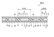
- FIG. 2 is a view showing a dye-sensitized solar cell according to an embodiment of the present invention, and is a cross-sectional view taken along the line AA shown in FIG.
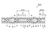
- FIG. 1 shows the 1st modification of the dye-sensitized solar cell which is one Embodiment of this invention, and is the cross section which looked at the position corresponding to the BB line
- FIG. 10 is a view showing a third modification of the dye-sensitized solar cell according to one embodiment of the present invention, and is a cross-sectional view taken along the line BB shown in FIG. 1 in the modification of the dye-sensitized solar cell.
- a semiconductor electrode (first electrode) 7 and a counter electrode (second electrode) 8 are arranged to face each other with a conductive material 6 interposed therebetween. This is an electrical module.
- a dye-sensitized solar cell 1A will be described as an example of an embodiment of the electric module 1 according to the present invention.
- this embodiment is provided between the first base material 2 and the second base material 4.
- the plurality of formed cells C are sealed, and the cells C, C. ..., it is applicable to various electric modules that require electrical series connection or parallel connection between C.
- the dye-sensitized solar cell 1 ⁇ / b> A includes a first base material 2, a second base material 4, a semiconductor electrode 7, a counter electrode 8, an electrolyte 9, and a conductive material 6. .
- the semiconductor electrode 7 includes a transparent conductive film 3 stacked on the first base material 2 and a porous semiconductor layer 10 stacked on the transparent conductive film 3.
- the counter electrode 8 includes a counter conductive film 5 stacked on the second substrate 4 and a catalyst layer 11 stacked on the counter conductive film 5.
- Sealing materials 12 and 12 are arranged on both sides of the conductive material 6 of the dye-sensitized solar cell 1A.
- the conductive material 6 and the sealing material 12 bond the electrodes (that is, between the semiconductor electrode 7 and the counter electrode 8).
- insulation and adhesion are performed by means such as ultrasonic fusion (hereinafter, the insulated portion is referred to as “insulating portion 13”).
- the cells C each having the semiconductor layer 10 are sealed in a liquid-tight manner.
- the conductive particles 20 included in the conductive material 6 form a gap in the thickness direction between the semiconductor electrode 7 and the counter electrode 8, and the electrolyte 9 is sealed in the gap.
- the conductive material 6 is in direct contact with the transparent conductive film 3 and the counter conductive film 5 constituting the semiconductor electrode 7 and the counter electrode 8.
- a plurality of patterning portions 25 insulated by laser irradiation or the like are provided at predetermined locations of the transparent conductive film 3 and the counter conductive film 5.
- the transparent conductive film 3 and the counter conductive film 5 between the adjacent cells C and C are divided into a plurality of parts by the patterning unit 25, and a pattern of the plurality of transparent conductive films 3 and the counter conductive film 5 is formed.
- the opposing conductive film 5 constituting the opposing electrode 8 of the first cell C1 and the transparent conductive film 3 constituting the semiconductor electrode 7 of the second cell C2 adjacent to the first cell C1.
- the first cell C1 and the second cell C2 are connected in series.
- the material of the first base material 2 and the second base material 4 is not particularly limited, and examples thereof include insulators such as resins, semiconductors, metals, and glass.
- the resin include poly (meth) acrylic acid ester, polycarbonate, polyester, polyimide, polystyrene, polyvinyl chloride, and polyamide.
- the substrate is preferably made of a transparent resin, more preferably a polyethylene terephthalate (PET) film or a polyethylene naphthalate (PEN) film.
- PET polyethylene terephthalate
- PEN polyethylene naphthalate
- the material of the 1st base material 2 and the material of the 2nd base material 4 may differ.
- the type and material of the transparent conductive film 3 and the counter conductive film 5 are not particularly limited, and a conductive film used for a known dye-sensitized solar cell is applicable.
- a thin film made of a metal oxide is used.
- the metal oxide include tin-doped indium oxide (ITO), fluorine-doped tin oxide (FTO), aluminum-doped zinc oxide (ATO), indium oxide / zinc oxide (IZO), and gallium-doped zinc oxide (GZO). it can.
- the semiconductor layer 10 is made of a material capable of receiving electrons from the adsorbed photosensitizing dye, and is usually preferably porous.
- the material which comprises the semiconductor layer 10 is not specifically limited, The material of the well-known semiconductor layer 10 is applicable, For example, metal oxide semiconductors, such as a titanium oxide, a zinc oxide, a tin oxide, are mentioned.
- the photosensitizing dye supported on the semiconductor layer 10 is not particularly limited, and examples thereof include known dyes such as organic dyes and metal complex dyes. Examples of the organic dye include coumarin, polyene, cyanine, hemicyanine, and thiophene. As said metal complex pigment
- the material constituting the catalyst layer 11 is not particularly limited, and known materials can be applied.
- carbons such as platinum and carbon nanotubes, poly (3,4-ethylenedioxythiophene) -poly (styrenesulfone)
- conductive polymers such as (acid) (PEDOT / PSS).
- Electrolyte 9 is not particularly limited, and an electrolyte used in a known dye-sensitized solar cell can be applied.
- Examples of the electrolyte 9 include an electrolytic solution in which iodine and sodium iodide are dissolved in an organic solvent.
- a known photosensitizing dye (not shown) is adsorbed on the surface including the porous interior.
- the conductive material 6 is disposed between the plurality of semiconductor layers 10 extending in parallel and in one direction, is in contact with the semiconductor electrode 7 on the first base material 2 and the counter electrode 8 on the second base material 4, and It is provided between the semiconductor electrode 7 and the counter electrode 8.
- the conductive material 6 is configured so that the conductive particles 20 are easily arranged in a single layer without overlapping in the thickness direction by leveling or pressurizing the conductive material 6 in application or disposition of the conductive material 6. Therefore, as shown in FIG. 3, the conductive particles 20 of the conductive material 6 are arranged in a single layer in the thickness direction between the transparent conductive film 3 and the counter conductive film 5 by a leveling operation such as pressurization. Yes. Note that the conductive particles 20 do not necessarily have to be arranged in a single layer between the transparent conductive film 3 and the counter conductive film 5.
- the conductive material 6 includes at least conductive particles 20.
- the conductive material 6 further includes a binder 18 and is obtained by curing the conductive paste.
- the conductive paste is also interpreted as the conductive material 6 in a broad sense.
- electrical_connection material 6 may suppress the fluidity
- a polymer binder used for forming a semiconductor layer of a known dye-sensitized solar cell is applicable, and examples thereof include ethyl cellulose, nitrocellulose, polyacrylic acid ester, and polyethylene glycol. It is done.
- the binder 18 one kind may be used alone, or two or more kinds may be used in combination, and even if the binder 18 is not a polymer, the fluidity may be moderately suppressed.
- the conductive particles 20 are a substance that is dispersed in a conductive paste and enables conduction between the electrodes of the dye-sensitized solar cell 1A.
- the conductive particles 20 may be electrically conductive, such as metal particles, and may be particles formed of a metal layer having at least a surface having conductivity.
- the conductive particles 20 enable conduction between the semiconductor electrode 7 and the counter electrode 8. Some or all of the conductive particles 20 are in contact with both the semiconductor electrode 7 and the counter electrode 8 and bite into at least one of the semiconductor electrode 7 and the counter electrode 8 as shown in FIGS. 2 and 3. .
- some or all of the conductive particles 20 penetrate through both or either of the semiconductor electrode 7 and the counter electrode 8, and / or both of the first substrate 2 and the second substrate 4. It is preferable to bite into one side.
- all of the conductive particles 20 penetrate both the semiconductor electrode 7 and the counter electrode 8 and bite into both the first base material 2 and the second base material 4.
- a dye-sensitized solar cell 1B shown in FIG. 4 is a first modification of the dye-sensitized solar cell 1A.
- part or all of the conductive particles 20 are in contact with both the semiconductor electrode 7 and the counter electrode 8, and both end portions in the thickness direction of the conductive particles 20 are both the semiconductor electrode 7 and the counter electrode 8 or It may be arranged inside either one. With such an arrangement, the surface of the conductive particle 20 and the surface of the semiconductor electrode 7 and the counter electrode 8 in the portion where the conductive particle 20 is embedded are reliably in contact with each other.
- the shape of the conductive particles 20 shown in FIGS. 2 and 4 is an example, and the shape of the conductive particles 20 is particularly limited if the conductive particles 20 can be disposed between the electrodes as described above and serve as a spacer. Not. Examples of the shape of such conductive particles include a polygonal shape, an elliptical shape, a needle shape, a star shape, and a substantially spherical shape.
- a dye-sensitized solar cell 1C shown in FIG. 5 is a second modification of the dye-sensitized solar cell 1A.
- the conductive particles 20 of the dye-sensitized solar cells 1A and 1B have a polygonal shape, whereas the conductive particles 20 of the dye-sensitized solar cell 1C are, for example, spherical as shown in FIG. Part or all of the spherical conductive particles 20 are in contact with both the semiconductor electrode 7 and the counter electrode 8, and both end portions in the thickness direction of the conductive particles 20 bite into both or either of the semiconductor electrode 7 and the counter electrode 8. It is out. That is, both or both ends of the conductive particles 20 in the thickness direction are located inside both the semiconductor electrode 7 and the counter electrode 8 or any one of them.
- the surface of the conductive particle 20 and the surface of the semiconductor electrode 7 and the counter electrode 8 where the conductive particle 20 is embedded are reliably in contact with each other.
- the conductive particles are resistant to bending of the entire dye-sensitized solar cell 1C. The position of 20 is not easily displaced, and the conduction between the conductive particles 20 and the semiconductor electrode 7 and the counter electrode 8 is reliably maintained.
- a dye-sensitized solar cell 1D shown in FIG. 6 is a third modification of the dye-sensitized solar cell 1A.
- the conductive particles 20 of the dye-sensitized solar cell 1D are, for example, spherical, like the conductive particles 20 of the dye-sensitized solar cell 1C.
- part or all of the spherical conductive particles 20 are in contact with both the semiconductor electrode 7 and the counter electrode 8. At least the semiconductor electrode 7 and the counter electrode 8 are extruded outward in the thickness direction by both end portions of the spherical conductive particles 20 in the thickness direction.
- the first substrate 2 and the second substrate 4 are also extruded outward in the thickness direction of the conductive particles 20.
- the semiconductor electrode 7 and the counter electrode 8 are pushed outward in the thickness direction by both ends in the thickness direction of the conductive particles 20, for example, the dye-sensitized solar cell 1C.
- the conductive particles 20 of the dye-sensitized solar cell 1 ⁇ / b> D are harder than the conductive particles 20, the semiconductor electrode 7 of the dye-sensitized solar cell 1 ⁇ / b> D is compared to the semiconductor electrode 7 and the counter electrode 8 of the dye-sensitized solar cell 1 ⁇ / b> C.
- the counter electrode 8 may be soft or highly elastic.
- the 1st base material 2 and the 2nd base material 4 are made into the thickness direction. Affix together at a predetermined interval. At this time, when the gap between the first base material 2 and the second base material 4 is narrowed and the conductive particles 20 are crushed so that the shape of the conductive particles 20 is restored after the bonding, the sealing material If 12 or the conductive material 6 is in an uncured state, the semiconductor electrode 7 and the counter electrode 8 may be pushed outward in the thickness direction by both ends of the conductive particles 20 in the thickness direction.
- the first substrate 2 and the second substrate 2 are crushed so that the conductive particles 20 are crushed by 10% or more of the average particle size, that is, the conductive particles 20 are crushed so that the thickness dimension of the conductive particles 20 is 90% or less of the average particle size.
- the semiconductor electrode 7 and the counter electrode 8 the first base material 2, and the second base material 4 are moderately directed outward in the thickness direction of the conductive particles 20 by both ends of the conductive particles 20 in the thickness direction. It is thought that it is pushed out.
- the first base material 2 and the second base material 4 are exposed from the outside of the first base material 2. It is considered that the force applied to 2 and the second substrate 4 is preferably 0.4 N or more per one conductive particle 20.
- the shape of the conductive particles 20 is not particularly limited as described above, and may be a polygonal shape, an elliptical shape, a needle shape, a star shape, or the like. Other shapes may be used. Even when the conductive particles 20 having such a shape other than the spherical shape are used, a part or all of both ends of the conductive particles 20 in the thickness direction are formed of the semiconductor electrode 7 and the counter electrode 8 as shown in FIG. As shown in FIG. 6, the semiconductor electrode 7 and the counter electrode 8 are at least partly or entirely in the thickness direction of both ends of the conductive particles 20 as shown in FIG. It can be in a state of being pushed outward in the thickness direction.
- the surface of the conductive particle 20 and the surface of the semiconductor electrode 7 and the counter electrode 8 where the conductive particle 20 is embedded are reliably in contact with each other. Further, since the semiconductor electrode 7 and the counter electrode 8 are in contact with the entire both ends of the conductive particle 20 in the thickness direction, the contact area between the conductive particle 20, the semiconductor electrode 7 and the counter electrode 8 is the dye-sensitized solar cell 1A, 1B. , 1C, and the conduction between the conductive particles 20, the semiconductor electrode 7 and the counter electrode 8 is more reliably maintained.
- both ends in the thickness direction of the conductive particles 20 are fixed at predetermined positions by the semiconductor electrode 7 and / or the counter electrode 8, the conductive particles can be bent even when the entire dye-sensitized solar cell 1D is bent.
- the position of 20 is not easily displaced, and the conduction between the conductive particles 20 and the semiconductor electrode 7 and the counter electrode 8 is reliably maintained.
- the average particle diameter of the conductive particles 20 is, for example, 5 ⁇ m or more and 500 ⁇ m or less.
- the conductive particles 20 having a desired average particle diameter are 1% by mass or more of a plurality of conductive substances included in the conductive paste. , Preferably 10% by weight or more, more preferably 40% by weight or more, still more preferably 70% by weight or more. Thereby, it becomes easy to keep the distance between electrodes constant.
- the distance between the semiconductor electrode 7 and the counter electrode 8 is appropriately set in consideration of physical properties such as elasticity of the conductive particles 20 used and the degree of variation in shape and particle diameter.
- the distance between the semiconductor electrode 7 and the counter electrode 8 is, for example, preferably 30% or more and 250% or less, more preferably 40% or more and 150% or less of the average particle diameter of the group of conductive particles 20, 50 % Is more preferably 120% or more and particularly preferably 60% or more and 90% or less.
- both end portions in the thickness direction of the conductive particles 20 are easily arranged inside the semiconductor electrode 7 and the counter electrode 8.
- the thickness interval between the semiconductor electrode 7 and the counter electrode 8 is the group of conductive particles 20.
- the conductive particles 20 penetrate the semiconductor electrode 7 and the counter electrode 8 and easily bite into the first base material 2 and the second base material 4.
- the material of the conductive particles 20 is not particularly limited as long as it has a hardness that can penetrate into the first base material 2 and the second base material 4, has conductivity, or can impart conductivity.
- Examples thereof include metal particles such as gold, silver, copper, chromium, titanium, platinum, nickel, tin, zinc, lead, tungsten, iron, and aluminum.
- grains which consist of electroconductive resin, or carbon-type particles, such as carbon black, are mentioned.
- grains etc. are mentioned.
- the conductive particles 20 are appropriately dispersed in the conductive paste, 99.9% by mass to 30% by mass of the binder 18 is included with respect to 0.1% by mass to 80% by mass of the conductive particles 20. It is preferable that By including the binder 18 and the conductive particles 20 in the conductive paste at such a mass ratio, the conductive particles 20 are appropriately dispersed in the conductive paste as described above, and the hardness of the conductive paste is arranged on the electrode. It will be a convenient level. Further, in the conductive paste and the conductive material 6, the conductive particles 20 suitable for achieving stable conduction between the electrodes can be held, and the conductive material 6 can be easily insulated or cut with ultrasonic waves or the like. , Conductive particles 20 are included. The conductive paste and the conductive material 6 may contain an appropriate amount of a thickening agent in order to increase the viscosity or prevent the conductive particles 20 made of metal particles from settling.
- a dye-sensitized solar cell 1A ′ shown in FIG. 7 is a fourth modification of the dye-sensitized solar cell 1A.
- the conductive material 6 preferably includes an auxiliary conductive material 21 in addition to the binder 18 and the conductive particles 20.
- the auxiliary conductive material 21 is in the form of particles, the conductive material 21 has a diameter smaller than the interval in the thickness direction between the electrodes when arranged in the conductive material 6 between the electrodes.
- 7 illustrates a configuration including the auxiliary conductive material 21 as a modification of the dye-sensitized solar cell 1A illustrated in FIGS. 1 to 3, but the dye-sensitized solar cell 1B illustrated in FIGS. , 1C, 1D can be applied to the same configuration.
- the average particle diameter of the auxiliary conductive material 21 is preferably 80% or less, for example, 50% or less of the average particle diameter of the conductive particles 20. Is more preferable, and it is still more preferable that it is 30% or less. Thereby, the above-mentioned purpose is achieved, and the conductivity of the conductive material 6 is further enhanced, so that the electrodes are electrically and stably electrically connected.
- the auxiliary conductive material 21 may be any material that has conductivity and does not hinder the conductivity of the conductive particles 20.
- Examples of the auxiliary conductive material 21 include particulate materials and fibers having a smaller diameter than the conductive particles 20.
- Examples of the material of the auxiliary conductive material 21 include metals such as gold, silver, copper, chromium, titanium, platinum, nickel, tin, zinc, lead, tungsten, iron, and aluminum, compounds containing these metals, conductive resins, or The thing which consists of carbon materials, such as carbon black, etc. are mentioned. The same substance as the conductive particles 20 may be used.
- the fiber diameter of the auxiliary conductive material 21 is preferably 45% or less and more preferably 30% or less with respect to the average particle size of the group of conductive particles 20. More preferably, it is 15% or less.
- the aspect ratio of the fiber length of the auxiliary conductive material 21 is, for example, about 2 or more and 500 or less. The fiber diameter and the aspect ratio can be adjusted as appropriate so as not to hinder the conductivity of the conductive particles 20.
- the shape and size of the auxiliary conductive material 21 may be uniform or non-uniform and are not particularly limited.
- the conductive paste may contain an adhesive, an adhesive, an organic solvent, a thickener, etc. in addition to the binder 18, the conductive particles 20, and the auxiliary conductive material 21.
- This adhesive has a function of maintaining a state in which the electrodes of the dye-sensitized solar cells 1A, 1B, 1C, 1D, and 1A ′ illustrated in FIGS. It is.
- the adhesive include, but are not limited to, resin materials including at least one thermoplastic resin, thermosetting resin, or ultraviolet curable resin.
- adhesive resin materials include vinyl acetate resin emulsion adhesives, ethylene / vinyl acetate copolymer resins, EVA (ethylene-vinyl acetate-vinyl chloride terpolymer) emulsion adhesives, ⁇ - Olefin (isobutene-maleic anhydride resin) adhesive, acrylic resin emulsion adhesive, styrene / butadiene rubber latex adhesive, vinyl acetate resin solvent adhesive, acrylic resin solvent adhesive, vinyl chloride Resin solvent type adhesive, chloroprene rubber type solvent type adhesive, chloroprene rubber type solvent type mastic type adhesive, nitrile rubber type solvent type adhesive, recycled rubber type solvent type styrene butadiene rubber (SBR) type Solvent-type adhesive, urethane resin-based adhesive, silicon Resin-based adhesive, modified silicone resin-based adhesive, epoxy / modified silicone resin-based adhesive, acrylic resin-based (second generation of acrylic adhesives: SGA) adhesive, starch-based adhesive, polymer cement
- an adhesive having a high viscosity can be used as an adhesive as long as it has a function of maintaining a state in which electrodes are arranged to face each other with a predetermined interval.
- the adhesive material having high viscosity include, but are not limited to, rubber-based, acrylic-based, silicone-based, and urethane-based materials. Specific examples include natural rubber, acrylate copolymer, silicone rubber, urethane resin, and the like.
- the organic solvent contained in the conductive paste is an auxiliary medium for maintaining the dispersed state of the conductive particles and the binder resin.
- organic solvents include, but are not limited to, water, ethyl acetate, ester-based, alcohol-based and ketone-based solvents, tetrahydrofuran, hexane, and aromatic solvents.
- the manufacturing method of the present embodiment is a manufacturing method of the dye-sensitized solar cell 1 ⁇ / b> A, in which the semiconductor electrode 7 and the counter electrode 8 are opposed to each other with an arbitrary distance, and between the semiconductor electrode 7 and the counter electrode 8. And a first step of arranging at least the conductive particles 20 and a second step of pressing and bonding the first base material and the second base material close to each other.
- each step will be specifically described.
- the counter conductive film 5 is formed at a predetermined position for forming cells on the second substrate 4 continuously conveyed in a predetermined direction P by using a known method for manufacturing a dye-sensitized solar cell. Thereafter, the catalyst layer 11 is formed at a predetermined position. Thereby, as shown in FIG. 9, the bonding base material 32 provided with the counter electrode 8 is obtained.
- the gap (between the first electrode and the second electrode) S of the bonded base material 31 contains at least the binder 18 and the conductive particles 20 from the conductive paste supply unit 34.
- the conductive material 6 is filled to make a conductive material 6.
- the conductive paste may be filled slightly thicker than a predetermined thickness in consideration of the fact that the sealing material 12 and the wiring material are crushed and expanded in the second step described later.
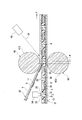
- the semiconductor layer 10 of the bonded base material 31 and the catalyst layer 11 of the bonded base material 32 are opposed to each other, and the bonded base material 31 and the bonded base material 32 are brought close to each other.
- the bonded base material (first base material) 31 and the bonded base material 31 are bonded.
- the laminated base material (second base material) 32 is pressed so as to be closer to each other.
- the bonded base material 31 and the bonded base material 32 are bonded together by irradiating the ultraviolet light UV vertically downward from the ultraviolet irradiation unit 46 and curing the sealing material 12 made of an ultraviolet curable resin. Thereafter, with the passage of time, the fluidity and the like of the conductive paste decreases and is cured appropriately. Thereby, dispersion
- the distance between the semiconductor electrode 7 and the counter electrode 8, that is, the thickness interval is preferably 30% or more and 250% or less, and 40% or more and 150% or less of the average particle diameter of the group of conductive particles 20. More preferably, it is 50% or more and 120%, more preferably 60% or more and 90% or less. Moreover, it is preferable to adjust appropriately the space
- the dye-sensitized solar cell 1A shown in FIGS. 1 and 3 is obtained by the first and second steps described above.
- the distance between the semiconductor electrode 7 and the counter electrode 8 is set in the thickness direction of at least a part of the conductive particles 20 in the second step.
- the method is the same as that of the dye-sensitized solar cell 1A described above, except that both ends are appropriately adjusted so as to be disposed in the semiconductor electrode 7 and the counter electrode 8.
- the manufacturing method of the dye-sensitized solar cell 1A ′ shown in FIG. 7 is the same as the manufacturing method of the dye-sensitized solar cell 1A described above, except that the auxiliary conductive material 21 is contained in the conductive paste.
- the electric module 1 exemplified by the dye-sensitized solar cells 1A, 1B, 1C, 1D, and 1A ′ described above and the manufacturing method thereof, at least between the semiconductor electrode 7 and the counter electrode 8 that constitute the electric module 1.
- the conductive paste containing the binder 18 and the conductive particles 20 is disposed, the conductive particles 20 are dispersed in the extending direction of the semiconductor electrode 7 and the counter electrode 8.
- the first base member 2 and the second base member 4 including the semiconductor electrode 7 and the counter electrode 8 are leveled by pressing and the like so as to be close to each other, and bonded, whereby the conductive particles 20 are placed on the same surface (that is, the electrode surface).
- One side) is easy to be arranged in a single layer.
- the conductive particles 20 are singularly (ie, in a single layer) interposed in the gap S in the thickness direction between the electrodes. .
- the part only of the binder 18 or adhesive agent between the electroconductive particles 20 of the extension direction of an electrode is comparatively soft, and can obtain the electric module 1 which is easy to cut
- the semiconductor electrode 7 is formed by a portion of the conductive particles 20 that bites into at least one of the semiconductor electrode 7 and the counter electrode 8 in the thickness direction between the semiconductor electrode 7 and the counter electrode 8. And the contact between the opposing electrodes 8 is obtained easily and reliably, and the electrodes are electrically connected. Furthermore, since the conductive particles 20 “bite into” at least one of the semiconductor electrode 7 and the counter electrode 8, the bonding strength between the conductive particles 20 and these electrodes is increased, and the conductive material 20 includes the conductive material 20 including the conductive particles 20.
- the electrical module 1 and the manufacturing method thereof the electrical performance of the electrical module 1 can be reliably maintained, and the quality of the electrical module 1 can be stably stabilized. That is, it is possible to obtain an electrical module 1 that can be easily electrically disconnected, can easily disconnect the conductive material 6 between the semiconductor electrode 7 and the counter electrode 8, and can conduct electricity between the electrodes with high stability. it can.
- the conductive particles 20 “bite into” the first base material 2 and / or the second base material 4.
- the thickness dimension at which the conductive particles 20 are in contact with the semiconductor electrode 7 and the counter electrode 8 is increased, and the bonding strength between the conductive particles 20 and these electrodes is further increased.
- a part or all of the conductive particles 20 penetrates both or one of the semiconductor electrode 7 and the counter electrode 8.
- the conduction between the conductive particles 20 and the semiconductor electrode 7 and the counter electrode 8 can be improved.
- the conductive performance of the dye-sensitized solar cells 1A, 1B, 1C, 1D, and 1A ' is more reliably maintained, and the quality of the dye-sensitized solar cells 1A, 1B, 1C, 1D, and 1A' is further improved. It can be well stabilized.
- a part or all of the distance between the semiconductor electrode 7 and the counter electrode 8 is set to be 30% or more and 250% or less of the average particle diameter of the group of conductive particles 20.
- the distance between the semiconductor electrode 7 and the counter electrode 8 can be made suitable so that the conductive particles 20 are in contact with both the semiconductor electrode 7 and the counter electrode 8 and bite into at least one of the semiconductor electrode 7 and the counter electrode 8. . Accordingly, only the binder 18 between the conductive particles 20 in the extending direction of the electrode can be made relatively soft and easy to cut.
- the conductive material 6 further includes the auxiliary conductive material 21, so that the auxiliary conductive material 21 is disposed in the gap between the conductive particles 20 between the electrodes, and the contact between the electrodes is provided. Furthermore, it can form easily and can conduct
- the conductive material 6 itself may serve as the sealing material 12 and may also serve as the sealing material 12.
- the conductive particles 20 and the conductive material 6 in which the conductive particles 20 are directly dispersed in the binder 18 are exemplified and described.
- the conductive particles 20 may be a suitable auxiliary material (not shown) or They may be held indirectly by an adhesive via a sealing material, and these may be integrated.
- the binder 18 may be omitted.
- a non-conductive material that can constitute such an auxiliary material for example, a resin material containing at least one resin such as a thermoplastic resin, a thermosetting resin, and an ultraviolet curable resin, or a fiber material constituting a known fiber , Materials such as cellulose and polyvinyl alcohol.
- a dye-sensitized solar cell 1D (see FIG. 6) was manufactured.
- Example 1 When manufacturing the dye-sensitized solar cell 1D, a micro pearl: AU100 (average diameter: 100 ⁇ m, manufacturer: Sekisui Chemical Co., Ltd.) is used as the conductive particles 20, and a compression tester (model number: DUH-W201, manufacturer: stock) In order to crush the conductive particles 20 from the outside in the thickness direction of the first base material 2 and the second base material 4 by Shimadzu Corporation, 0.4N per one of the conductive particles 20 was applied and bonded together. In the obtained dye-sensitized solar cell 1D, as shown in FIG. 6, the semiconductor electrode 7 and the counter electrode 8 are extruded outward in the thickness direction of the conductive particles 20 by both ends of the conductive particles 20 in the thickness direction.
- Convex portions were formed on the first base material 2 and the second base material 4 of the wiring portion where 20 was disposed.
- the convex portions have substantially the same shape as the spherical notches at both ends in the thickness direction of the substantially spherical micropearl that is the conductive particles 20, and rise from the respective surfaces of the first base material 2 and the second base material 4. It is a part that.
- the rearward in the crushing direction that is, the upper side in FIG. 6.
- the dimension of the second substrate 4 side) to be pushed outward in the thickness direction of the conductive particles 20 was increased.
- the bonding strength between the conductive particles 20 and the semiconductor electrode 7 or the counter electrode 8 can be increased. Seem.
- Example 2 A dye-sensitized solar cell 1D was produced in the same manner as in Example 1 except that copper powder having an acicular shape (average dimension of the longest part: 90 ⁇ m) was used as the conductive particles 20. Also in the dye-sensitized solar cell 1D of Example 2, convex portions were formed on the first base material 2 and the second base material 4 of the wiring portion where the conductive particles 20 were arranged. In the convex portion, it was confirmed that both end portions of the conductive particles 20 in the thickness direction bite into the semiconductor electrode 7 and the counter electrode 8 and also bite into the first base material 2 and the second base material.
- SYMBOLS 1 Electric module, 1A, 1B, 1C, 1D, 1A ', 1B ... Dye-sensitized solar cell (electric module), 2 ... First base material, 4 ... Second base material, 6 ... Conductive material, 7 ... Semiconductor Electrode (first electrode), 8 ... Counter electrode (second electrode), 18 ... Binder, 20 ... Conductive particles, 21 ... Auxiliary conductive material
Landscapes
- Engineering & Computer Science (AREA)
- Power Engineering (AREA)
- Microelectronics & Electronic Packaging (AREA)
- Manufacturing & Machinery (AREA)
- Hybrid Cells (AREA)
- Photovoltaic Devices (AREA)
Abstract
Description
上述の問題を解決する一方法として、接着剤に導電性フィラーを備えた導電性ペーストを用いて電気的な接続を図る方法が知られている。
また、電極間の厚み方向において、導電粒子のうち第一電極と第二電極の少なくとも一方に食い込んでいる部分によって電極間の接点が容易且つ確実に得られ、電極同士が導通される。さらに、導電粒子が第一電極と第二電極の少なくとも一方に「食い込んでいる」ことによって、導電粒子と電極との接合強度が高まり、電極が導電粒子を含む導通材から剥がれ難くなり、電極と導通材との相対位置関係がずれ難くなると共に、電極間の厚み寸法が長期にわたり一定に保たれる。これにより、電気モジュールの導電性能が確実に保持され、品質が良好に安定する。
このような原理に基づいた色素増感型の電気モジュールが得られ、その導電性能がより確実に保持され、品質がより良好に安定する。
上述の工程によれば、例えば、電気モジュールを構成する電極間に本発明の導電性ペースト(導電材)を配した際に、電極の延在方向に導電粒子が分散される。これにより、電極の延在方向の導電粒子同士の間は比較的柔らかくなるので、切断し易い電気モジュールが得られる。
また、第二工程において、第一基材と第二基材が貼り合される際に、第一基材と第二基材とが互いに近づけるように押圧されることで、電極間の厚み方向において、導電粒子が第一電極と第二電極の少なくとも一方に食い込む。電極間の接点が容易且つ確実に得られ、電極同士が導通され、導電粒子が第一電極と第二電極の少なくとも一方に「食い込む」ことによって、導電粒子と電極との接合強度が高まる。従って、電気モジュールの導電性能が確実に保持され、品質が良好に安定する。
図1から図3に示すように、色素増感太陽電池(電気モジュール)1Aは、半導体電極(第一電極)7と対向電極(第二電極)8とが導通材6を介して対向配置されてなる電気モジュールである。
対向電極8は、第二基材4上に積層された対向導電膜5と、対向導電膜5上に積層された触媒層11と、を備えている。
半導体層10に担持される光増感色素は特に限定されず、例えば有機色素、金属錯体色素等の公知の色素が挙げられる。前述の有機色素としては、例えば、クマリン系、ポリエン系、シアニン系、ヘミシアニン系、チオフェン系等が挙げられる。前記金属錯体色素としては、例えば、ルテニウム錯体等が好適に用いられる。
導通材6は、導通材6の塗工又は配設において均したり加圧したりすることで、導電粒子20が厚さ方向に重なることなく単層で配されやすく構成されている。従って、導通材6の導電粒子20は、図3に示すように、透明導電膜3と対向導電膜5との間に、加圧等の均す作業により厚さ方向に単層で配されている。なお、導電粒子20は、透明導電膜3と対向導電膜5との間に必ずしも単層で配されていなくてもよい。
バインダー18は、一種を単独で使用してもよいし、二種以上を併用してもよく、高分子でなくとも、流動性が適度に抑えられていればよい。
このような配置により、導電粒子20の表面と導電粒子20が貫通した部分の半導体電極7ならびに対向電極8の内壁とが確実に接触すると共に、導電粒子20の厚み方向両端部が第一基材2ならびに第二基材4の内部に埋め込まれた状態とされている。
図4に示すように、導電粒子20の一部又は全部は、半導体電極7と対向電極8との両方に接し、導電粒子20の厚み方向の両端部が半導体電極7ならびに対向電極8の双方もしくは何れか一方の内部に配置されていてもよい。
このような配置により、導電粒子20の表面と導電粒子20が埋め込まれた部分の半導体電極7ならびに対向電極8の表面とが確実に接触する。
色素増感太陽電池1A,1Bの導電粒子20が多角体形状であるのに対し、図5に示すように、色素増感太陽電池1Cの導電粒子20は、例えば球状である。球状の導電粒子20の一部又は全部は、半導体電極7と対向電極8との両方に接し、導電粒子20の厚み方向の両端部が半導体電極7ならびに対向電極8の双方もしくは何れか一方に食い込んでいる。即ち、導電粒子20の一部又は全部の厚み方向の両端部が半導体電極7ならびに対向電極8の双方もしくは何れか一方の内方に位置している。
色素増感太陽電池1Dの導電粒子20は、色素増感太陽電池1Cの導電粒子20と同様に例えば球状である。図6に示すように、球状の導電粒子20の一部又は全部は、半導体電極7と対向電極8との両方に接している。少なくとも半導体電極7と対向電極8は、球状の導電粒子20の厚み方向の両端部によって厚み方向外方に押し出されている。図6に例示する構成では、第一基材2及び第二基材4も導電粒子20の厚み方向外方に押し出されている。
なお、導電性ペースト中に導電粒子20の他に導電性物質が含まれる場合、所望の平均粒子径を有する導電粒子20は、導電性ペーストに含まれる複数の導電性物質のうち1質量%以上、好ましくは10重量%以上、より好ましくは40重量%以上、さらに好ましくは70重量%以上含まれている。これにより、電極間の距離が一定に保持され易くなる。
図7に示すように、導通材6は、バインダー18と、導電粒子20との他に、補助導電物質21を備えていることが好ましい。例えば補助導電物質21が粒子状であれば、電極間に導通材6に含まれて配置された際に、電極間の厚み方向の間隔よりも小さい径寸法を有する。なお、図7では、図1から図3に示す色素増感太陽電池1Aの変形例として補助導電物質21を備えている構成を例示するが、図4から図6に示す色素増感太陽電池1B,1C,1Dにも同様の構成を適用することができる。
補助導電物質21の材料としては、金、銀、銅、クロム、チタン、白金、ニッケル、錫、亜鉛、鉛、タングステン、鉄、アルミニウム等の金属、これらの金属を含む化合物、導電性樹脂、又はカーボンブラック等の炭素材料からなるもの等が挙げられる。導電粒子20と同一の物質であってもよい。
補助導電物質21の形状や大きさは、均一でも不均一でもよく、特に限定されない。
次いで、本発明に係る電気モジュール1の製造方法の一実施形態について、色素増感太陽電池1Aの製造方法(以下、単に「製造方法」ともいう。)を例に挙げて説明する。
先ず、ロール・ツー・ロール方式を用いた公知の色素増感太陽電池の製造方法を用いて、所定の方向Pに連続搬送される第一基材2上のセルを形成するための所定の位置に透明導電膜3を形成し、その後、所定の位置に半導体層10を形成し、半導体層10の両側(即ち、周囲)に封止材12を形成した後、電解質9を積層する。これにより、図8に示すように、半導体電極7及び封止材12を備えると共に、適所に隙間Sが形成された貼り合わせ基材31を得る。なお、所定の方向Pは製造上の都合等を勘案して自由に設定されればよく、例えば導通材6の延在方向に平行な方向であってもよい。
続いて図10に示すように、貼り合わせ基材31の半導体層10と貼り合わせ基材32の触媒層11とを対向させ、貼り合わせ基材31と貼り合わせ基材32とを互いに近づける。貼り合わせ基材31,32の厚み方向に所定の間隔をあけた状態で該厚み方向に沿って配置され一対のローラー41,42を用いて、貼り合わせ基材(第一基材)31と貼り合わせ基材(第二基材)32とを互いにより近づけるように押圧する。紫外線照射部46から紫外線UVを鉛直下向きに照射し、紫外線硬化樹脂からなる封止材12を硬化させることで貼り合わせ基材31と貼り合わせ基材32とを貼り合わせる。この後、時間の経過に伴って、導電性ペーストの流動性等が低下し、適度に硬化される。これにより、導通材6における導電粒子20の分散等が安定する。
なお、図4から図6に示す色素増感太陽電池1B,1C,1Dの製造方法は、第二工程において半導体電極7と対向電極8との距離を導電粒子20の少なくとも一部の厚み方向の両端部が半導体電極7ならびに対向電極8内に配されるように適宜調整すること以外は、上述した色素増感太陽電池1Aの製造方法と同様である。また、図7に示す色素増感太陽電池1A´の製造方法は、導電性ペーストに補助導電物質21が含有されること以外は、上述した色素増感太陽電池1Aの製造方法と同様である。
色素増感太陽電池1Dを製造する際に、導電粒子20としてミクロパール:AU100(平均直径:100μm、製造元:積水化学工業株式会社)を用い、圧縮試験機(型番:DUH-W201、製造元:株式会社島津製作所)によって第一基材2及び第二基材4の厚み方向外方から導電粒子20を押し潰すように、導電粒子20の一つ当たり0.4Nの力を加えて貼り合わせた。得られた色素増感太陽電池1Dでは、図6に示すように、半導体電極7と対向電極8が導電粒子20の厚み方向の両端部によって導電粒子20の厚み方向外方に押し出され、導電粒子20を配置した配線部分の第一基材2及び第二基材4に凸部分が形成された。この凸部分は、導電粒子20である略球状のミクロパールの厚み方向の両端部の球欠と略同様の形状を有し、第一基材2及び第二基材4のそれぞれの表面から盛り上がっている部分である。また、本実施例では、押し潰す方向において前方(すなわち、図6における下側であって、第一基材2の側)に比べて、押し潰す方向において後方(すなわち、図6における上側であって、第二基材4の側)の方が導電粒子20の厚み方向外方に押し出される寸法が大きくなった。
このように、0.4Nの力を加えて第一基材2及び第二基材4を貼り合わせた場合、導電粒子20と半導体電極7又は対向電極8との接合強度を高めることができると思われる。
導電粒子20として針状形状を有する銅粉末(最長部の平均寸法:90μm)を用いたこと以外は実施例1と同様にして、色素増感太陽電池1Dを製造した。実施例2の色素増感太陽電池1Dにおいても、導電粒子20を配置した配線部分の第一基材2及び第二基材4に凸部分が形成された。凸部分では、導電粒子20の厚み方向の両端部が半導体電極7及び対向電極8に食い込み、第一基材2及び第二基材にも食い込んでいることを確認した。
上述の実施例1及び実施例2に対し、色素増感太陽電池1Dを製造する際に、導電粒子20として柔軟なコアを有するミクロパール(平均直径:100μm、製造元:積水化学工業株式会社)、すなわち実施例1で用いたミクロパールとはコアのみ異なる該ミクロパールの類似品(平均直径:100μm、製造元:積水化学工業(株))を用い、上述の圧縮試験機によって第一基材2及び第二基材4の厚み方向外方から導電粒子20を押し潰すように0.065Nの力を加えて貼り合わせた。得られた色素増感太陽電池1Dでは、凸部分は形成されなかった。
このように、0.065Nの力を加えて第一基材2及び第二基材4を貼り合わせた場合、導電粒子20を配置した配線部分の導電粒子20と半導体電極7又は対向電極8とが接合していない部分が存在する虞があり、導電粒子20と半導体電極7又は対向電極8との接合強度を高めることが難しいと思われる。
Claims (9)
- 第一基材上の第一電極と第二基材上の第二電極とに接し、且つ前記第一電極と前記第二電極との間に設けられた導通材を備え、
前記導通材は、前記第一電極と前記第二電極との間を導通可能とする導電粒子を含み、
一部又は全部の前記導電粒子は、前記第一電極と前記第二電極との両方に接し、且つ前記第一電極と前記第二電極の少なくとも一方に食い込んでいる電気モジュール。 - 前記の一部又は全部の導電粒子は、前記第一電極ならびに前記第二電極の双方もしくは何れか一方を貫通している請求項1に記載の電気モジュール。
- 前記の一部又は全部の導電粒子は、前記第一電極と前記第二電極との両方に接し、且つ前記第一基材ならびに前記第二基材の双方もしくは何れか一方に食い込んでいる請求項1又は請求項2に記載の電気モジュール。
- 前記第一電極と前記第二電極との距離は、前記導電粒子の群の平均粒子径の30%以上250%以下である請求項1から請求項3の何れか一項に記載の電気モジュール。
- 前記導通材は前記第一電極と前記第二電極との間の厚み方向の間隔よりも小さい径寸法の補助導電物質をさらに含む請求項1から請求項4の何れか一項に記載の電気モジュール。
- 前記第一電極又は前記第二電極が光増感色素を含む請求項1から請求項5の何れか一項に記載の電気モジュール。
- 請求項1から請求項6に記載の何れか一項に記載の電気モジュールの製造方法であって、
前記第一電極と前記第二電極とを任意の距離を空けて対向させ、前記第一電極と前記第二電極との間に、少なくとも前記導電粒子を配する第一工程と、
前記第一基材と前記第二基材とを互いに近づけるように押圧し、前記第一基材と前記第二基材とを貼り合わせる第二工程と、を備える電気モジュールの製造方法。 - 前記第二工程は、前記第一電極と前記第二電極との距離を前記導電粒子の群の平均粒子径の30%以上250%以下とする請求項7に記載の電気モジュールの製造方法。
- 前記第二工程において、前記第一基材と前記第二基材とを互いに近づけるように、前記導電粒子の一つ当たり0.4N以上の力で押圧する請求項7又は請求項8に記載の電気モジュールの製造方法。
Priority Applications (3)
| Application Number | Priority Date | Filing Date | Title |
|---|---|---|---|
| JP2018500236A JP6916162B2 (ja) | 2016-02-18 | 2017-02-17 | 電気モジュール及び電気モジュールの製造方法 |
| KR1020187017815A KR20180113979A (ko) | 2016-02-18 | 2017-02-17 | 전기 모듈 및 전기 모듈의 제조 방법 |
| CN201780005230.9A CN108475583A (zh) | 2016-02-18 | 2017-02-17 | 电组件及电组件的制造方法 |
Applications Claiming Priority (4)
| Application Number | Priority Date | Filing Date | Title |
|---|---|---|---|
| JP2016028968 | 2016-02-18 | ||
| JP2016-028968 | 2016-02-18 | ||
| JP2016161884 | 2016-08-22 | ||
| JP2016-161884 | 2016-08-22 |
Publications (1)
| Publication Number | Publication Date |
|---|---|
| WO2017142086A1 true WO2017142086A1 (ja) | 2017-08-24 |
Family
ID=59626112
Family Applications (1)
| Application Number | Title | Priority Date | Filing Date |
|---|---|---|---|
| PCT/JP2017/005998 Ceased WO2017142086A1 (ja) | 2016-02-18 | 2017-02-17 | 電気モジュール及び電気モジュールの製造方法 |
Country Status (5)
| Country | Link |
|---|---|
| JP (1) | JP6916162B2 (ja) |
| KR (1) | KR20180113979A (ja) |
| CN (1) | CN108475583A (ja) |
| TW (1) | TW201737501A (ja) |
| WO (1) | WO2017142086A1 (ja) |
Cited By (3)
| Publication number | Priority date | Publication date | Assignee | Title |
|---|---|---|---|---|
| WO2018174247A1 (ja) * | 2017-03-24 | 2018-09-27 | 積水化学工業株式会社 | 太陽電池モジュール、太陽電池モジュールの製造方法 |
| JP2020038877A (ja) * | 2018-09-03 | 2020-03-12 | 積水化学工業株式会社 | 電気モジュールおよび電気モジュールの製造方法 |
| JP2020038876A (ja) * | 2018-09-03 | 2020-03-12 | 積水化学工業株式会社 | 電気モジュール |
Families Citing this family (1)
| Publication number | Priority date | Publication date | Assignee | Title |
|---|---|---|---|---|
| KR102415359B1 (ko) | 2020-10-26 | 2022-07-01 | 한국해양대학교 산학협력단 | 해양탐사 수신센서 심도유지를 위한 수중예인장치 및 그 동작 방법 |
Citations (6)
| Publication number | Priority date | Publication date | Assignee | Title |
|---|---|---|---|---|
| JP2001357897A (ja) * | 2000-06-14 | 2001-12-26 | Fuji Xerox Co Ltd | 光電変換モジュール |
| JP2002322456A (ja) * | 2001-04-23 | 2002-11-08 | Asahi Glass Co Ltd | 異方性導電ペースト |
| JP2003243052A (ja) * | 2002-02-13 | 2003-08-29 | Canon Inc | 光電変換モジュール |
| WO2009017200A1 (ja) * | 2007-08-02 | 2009-02-05 | Hitachi Chemical Company, Ltd. | 回路接続材料、それを用いた回路部材の接続構造及び回路部材の接続方法 |
| WO2009057704A1 (ja) * | 2007-11-02 | 2009-05-07 | Nippon Kayaku Kabushiki Kaisha | 色素増感太陽電池モジュール |
| JP2012164454A (ja) * | 2011-02-04 | 2012-08-30 | Sony Chemical & Information Device Corp | 導電性粒子及びこれを用いた異方性導電材料 |
Family Cites Families (2)
| Publication number | Priority date | Publication date | Assignee | Title |
|---|---|---|---|---|
| JP4467721B2 (ja) * | 2000-06-26 | 2010-05-26 | 富士通マイクロエレクトロニクス株式会社 | コンタクタ及びコンタクタを使用した試験方法 |
| JP4737179B2 (ja) * | 2007-11-02 | 2011-07-27 | トヨタ自動車株式会社 | 車両制御装置及び車両制御方法 |
-
2017
- 2017-02-17 CN CN201780005230.9A patent/CN108475583A/zh active Pending
- 2017-02-17 TW TW106105248A patent/TW201737501A/zh unknown
- 2017-02-17 WO PCT/JP2017/005998 patent/WO2017142086A1/ja not_active Ceased
- 2017-02-17 JP JP2018500236A patent/JP6916162B2/ja not_active Expired - Fee Related
- 2017-02-17 KR KR1020187017815A patent/KR20180113979A/ko not_active Ceased
Patent Citations (6)
| Publication number | Priority date | Publication date | Assignee | Title |
|---|---|---|---|---|
| JP2001357897A (ja) * | 2000-06-14 | 2001-12-26 | Fuji Xerox Co Ltd | 光電変換モジュール |
| JP2002322456A (ja) * | 2001-04-23 | 2002-11-08 | Asahi Glass Co Ltd | 異方性導電ペースト |
| JP2003243052A (ja) * | 2002-02-13 | 2003-08-29 | Canon Inc | 光電変換モジュール |
| WO2009017200A1 (ja) * | 2007-08-02 | 2009-02-05 | Hitachi Chemical Company, Ltd. | 回路接続材料、それを用いた回路部材の接続構造及び回路部材の接続方法 |
| WO2009057704A1 (ja) * | 2007-11-02 | 2009-05-07 | Nippon Kayaku Kabushiki Kaisha | 色素増感太陽電池モジュール |
| JP2012164454A (ja) * | 2011-02-04 | 2012-08-30 | Sony Chemical & Information Device Corp | 導電性粒子及びこれを用いた異方性導電材料 |
Cited By (5)
| Publication number | Priority date | Publication date | Assignee | Title |
|---|---|---|---|---|
| WO2018174247A1 (ja) * | 2017-03-24 | 2018-09-27 | 積水化学工業株式会社 | 太陽電池モジュール、太陽電池モジュールの製造方法 |
| JP2020038877A (ja) * | 2018-09-03 | 2020-03-12 | 積水化学工業株式会社 | 電気モジュールおよび電気モジュールの製造方法 |
| JP2020038876A (ja) * | 2018-09-03 | 2020-03-12 | 積水化学工業株式会社 | 電気モジュール |
| JP7107788B2 (ja) | 2018-09-03 | 2022-07-27 | 積水化学工業株式会社 | 電気モジュールおよび電気モジュールの製造方法 |
| JP7164362B2 (ja) | 2018-09-03 | 2022-11-01 | 積水化学工業株式会社 | 電気モジュール |
Also Published As
| Publication number | Publication date |
|---|---|
| JP6916162B2 (ja) | 2021-08-11 |
| JPWO2017142086A1 (ja) | 2018-12-06 |
| KR20180113979A (ko) | 2018-10-17 |
| TW201737501A (zh) | 2017-10-16 |
| CN108475583A (zh) | 2018-08-31 |
Similar Documents
| Publication | Publication Date | Title |
|---|---|---|
| JP6626494B2 (ja) | 電気モジュール及び電気モジュールの製造方法 | |
| JP6916162B2 (ja) | 電気モジュール及び電気モジュールの製造方法 | |
| CN102176482B (zh) | 粘接带及使用其的太阳能电池模块 | |
| CN207009539U (zh) | 极片及电芯 | |
| CN103901692B (zh) | 电致变色结构 | |
| JP5446420B2 (ja) | 太陽電池モジュール及びその製造方法 | |
| CN103050170A (zh) | 各向异性导电膜片及其制作方法 | |
| CN102483969A (zh) | 太阳能电池集流条与太阳能电池主栅的连接以及由此制得的太阳能电池 | |
| CN109478468B (zh) | 太阳能电池模块及太阳能电池模块的制造方法 | |
| JPWO2009057704A1 (ja) | 色素増感太陽電池モジュール | |
| CN108323213A (zh) | 光伏模块互连接头 | |
| Jo et al. | Plasticized polymer interlayer for low-temperature fabrication of a high-quality silver nanowire-based flexible transparent and conductive film | |
| CN105097068B (zh) | 导电胶、太阳能电池串及其制备方法 | |
| JP2018128595A (ja) | 調光フィルム、及びそれを用いた調光装置並びにスクリーン | |
| JP2013508912A (ja) | 箔(ホイル)を用いた染料感応太陽電池モジュールの製造方法およびこれによって製造される染料感応太陽電池モジュール | |
| US20120085383A1 (en) | Solar cell module and method of manufacturing the same | |
| US20130129935A1 (en) | Highly Transparent and Electrically Conductive Substrate | |
| JP5692347B2 (ja) | 導電接着剤 | |
| CN210073349U (zh) | 一种导电膜 | |
| CN105593947A (zh) | 背接触式的太阳能电池模块用导电性粒子、导电材料及太阳能电池模块 | |
| WO2015105120A1 (ja) | バックコンタクト方式の太陽電池モジュール用導電性粒子、導電材料及び太陽電池モジュール | |
| JP6008184B2 (ja) | 太陽電池 | |
| JP2020126875A (ja) | 電気モジュール及びその製造方法 | |
| JP2020126876A (ja) | 電気モジュール | |
| JP2017059832A (ja) | 太陽電池 |
Legal Events
| Date | Code | Title | Description |
|---|---|---|---|
| 121 | Ep: the epo has been informed by wipo that ep was designated in this application |
Ref document number: 17753340 Country of ref document: EP Kind code of ref document: A1 |
|
| ENP | Entry into the national phase |
Ref document number: 20187017815 Country of ref document: KR Kind code of ref document: A |
|
| WWE | Wipo information: entry into national phase |
Ref document number: 2018500236 Country of ref document: JP |
|
| NENP | Non-entry into the national phase |
Ref country code: DE |
|
| 122 | Ep: pct application non-entry in european phase |
Ref document number: 17753340 Country of ref document: EP Kind code of ref document: A1 |