WO2017138185A1 - 基板処理装置、基板保持具及び載置具 - Google Patents
基板処理装置、基板保持具及び載置具 Download PDFInfo
- Publication number
- WO2017138185A1 WO2017138185A1 PCT/JP2016/078220 JP2016078220W WO2017138185A1 WO 2017138185 A1 WO2017138185 A1 WO 2017138185A1 JP 2016078220 W JP2016078220 W JP 2016078220W WO 2017138185 A1 WO2017138185 A1 WO 2017138185A1
- Authority
- WO
- WIPO (PCT)
- Prior art keywords
- substrate
- support
- column
- mounting
- support column
- Prior art date
- Legal status (The legal status is an assumption and is not a legal conclusion. Google has not performed a legal analysis and makes no representation as to the accuracy of the status listed.)
- Ceased
Links
Images





Classifications
-
- H—ELECTRICITY
- H10—SEMICONDUCTOR DEVICES; ELECTRIC SOLID-STATE DEVICES NOT OTHERWISE PROVIDED FOR
- H10P—GENERIC PROCESSES OR APPARATUS FOR THE MANUFACTURE OR TREATMENT OF DEVICES COVERED BY CLASS H10
- H10P72/00—Handling or holding of wafers, substrates or devices during manufacture or treatment thereof
- H10P72/04—Apparatus for manufacture or treatment
- H10P72/0402—Apparatus for fluid treatment
-
- H—ELECTRICITY
- H10—SEMICONDUCTOR DEVICES; ELECTRIC SOLID-STATE DEVICES NOT OTHERWISE PROVIDED FOR
- H10P—GENERIC PROCESSES OR APPARATUS FOR THE MANUFACTURE OR TREATMENT OF DEVICES COVERED BY CLASS H10
- H10P72/00—Handling or holding of wafers, substrates or devices during manufacture or treatment thereof
- H10P72/70—Handling or holding of wafers, substrates or devices during manufacture or treatment thereof for supporting or gripping
-
- C—CHEMISTRY; METALLURGY
- C23—COATING METALLIC MATERIAL; COATING MATERIAL WITH METALLIC MATERIAL; CHEMICAL SURFACE TREATMENT; DIFFUSION TREATMENT OF METALLIC MATERIAL; COATING BY VACUUM EVAPORATION, BY SPUTTERING, BY ION IMPLANTATION OR BY CHEMICAL VAPOUR DEPOSITION, IN GENERAL; INHIBITING CORROSION OF METALLIC MATERIAL OR INCRUSTATION IN GENERAL
- C23C—COATING METALLIC MATERIAL; COATING MATERIAL WITH METALLIC MATERIAL; SURFACE TREATMENT OF METALLIC MATERIAL BY DIFFUSION INTO THE SURFACE, BY CHEMICAL CONVERSION OR SUBSTITUTION; COATING BY VACUUM EVAPORATION, BY SPUTTERING, BY ION IMPLANTATION OR BY CHEMICAL VAPOUR DEPOSITION, IN GENERAL
- C23C16/00—Chemical coating by decomposition of gaseous compounds, without leaving reaction products of surface material in the coating, i.e. chemical vapour deposition [CVD] processes
- C23C16/22—Chemical coating by decomposition of gaseous compounds, without leaving reaction products of surface material in the coating, i.e. chemical vapour deposition [CVD] processes characterised by the deposition of inorganic material, other than metallic material
- C23C16/30—Deposition of compounds, mixtures or solid solutions, e.g. borides, carbides, nitrides
- C23C16/34—Nitrides
-
- C—CHEMISTRY; METALLURGY
- C23—COATING METALLIC MATERIAL; COATING MATERIAL WITH METALLIC MATERIAL; CHEMICAL SURFACE TREATMENT; DIFFUSION TREATMENT OF METALLIC MATERIAL; COATING BY VACUUM EVAPORATION, BY SPUTTERING, BY ION IMPLANTATION OR BY CHEMICAL VAPOUR DEPOSITION, IN GENERAL; INHIBITING CORROSION OF METALLIC MATERIAL OR INCRUSTATION IN GENERAL
- C23C—COATING METALLIC MATERIAL; COATING MATERIAL WITH METALLIC MATERIAL; SURFACE TREATMENT OF METALLIC MATERIAL BY DIFFUSION INTO THE SURFACE, BY CHEMICAL CONVERSION OR SUBSTITUTION; COATING BY VACUUM EVAPORATION, BY SPUTTERING, BY ION IMPLANTATION OR BY CHEMICAL VAPOUR DEPOSITION, IN GENERAL
- C23C16/00—Chemical coating by decomposition of gaseous compounds, without leaving reaction products of surface material in the coating, i.e. chemical vapour deposition [CVD] processes
- C23C16/44—Chemical coating by decomposition of gaseous compounds, without leaving reaction products of surface material in the coating, i.e. chemical vapour deposition [CVD] processes characterised by the method of coating
- C23C16/455—Chemical coating by decomposition of gaseous compounds, without leaving reaction products of surface material in the coating, i.e. chemical vapour deposition [CVD] processes characterised by the method of coating characterised by the method used for introducing gases into reaction chamber or for modifying gas flows in reaction chamber
- C23C16/45523—Pulsed gas flow or change of composition over time
- C23C16/45525—Atomic layer deposition [ALD]
-
- C—CHEMISTRY; METALLURGY
- C23—COATING METALLIC MATERIAL; COATING MATERIAL WITH METALLIC MATERIAL; CHEMICAL SURFACE TREATMENT; DIFFUSION TREATMENT OF METALLIC MATERIAL; COATING BY VACUUM EVAPORATION, BY SPUTTERING, BY ION IMPLANTATION OR BY CHEMICAL VAPOUR DEPOSITION, IN GENERAL; INHIBITING CORROSION OF METALLIC MATERIAL OR INCRUSTATION IN GENERAL
- C23C—COATING METALLIC MATERIAL; COATING MATERIAL WITH METALLIC MATERIAL; SURFACE TREATMENT OF METALLIC MATERIAL BY DIFFUSION INTO THE SURFACE, BY CHEMICAL CONVERSION OR SUBSTITUTION; COATING BY VACUUM EVAPORATION, BY SPUTTERING, BY ION IMPLANTATION OR BY CHEMICAL VAPOUR DEPOSITION, IN GENERAL
- C23C16/00—Chemical coating by decomposition of gaseous compounds, without leaving reaction products of surface material in the coating, i.e. chemical vapour deposition [CVD] processes
- C23C16/44—Chemical coating by decomposition of gaseous compounds, without leaving reaction products of surface material in the coating, i.e. chemical vapour deposition [CVD] processes characterised by the method of coating
- C23C16/455—Chemical coating by decomposition of gaseous compounds, without leaving reaction products of surface material in the coating, i.e. chemical vapour deposition [CVD] processes characterised by the method of coating characterised by the method used for introducing gases into reaction chamber or for modifying gas flows in reaction chamber
- C23C16/45587—Mechanical means for changing the gas flow
- C23C16/45591—Fixed means, e.g. wings, baffles
-
- C—CHEMISTRY; METALLURGY
- C23—COATING METALLIC MATERIAL; COATING MATERIAL WITH METALLIC MATERIAL; CHEMICAL SURFACE TREATMENT; DIFFUSION TREATMENT OF METALLIC MATERIAL; COATING BY VACUUM EVAPORATION, BY SPUTTERING, BY ION IMPLANTATION OR BY CHEMICAL VAPOUR DEPOSITION, IN GENERAL; INHIBITING CORROSION OF METALLIC MATERIAL OR INCRUSTATION IN GENERAL
- C23C—COATING METALLIC MATERIAL; COATING MATERIAL WITH METALLIC MATERIAL; SURFACE TREATMENT OF METALLIC MATERIAL BY DIFFUSION INTO THE SURFACE, BY CHEMICAL CONVERSION OR SUBSTITUTION; COATING BY VACUUM EVAPORATION, BY SPUTTERING, BY ION IMPLANTATION OR BY CHEMICAL VAPOUR DEPOSITION, IN GENERAL
- C23C16/00—Chemical coating by decomposition of gaseous compounds, without leaving reaction products of surface material in the coating, i.e. chemical vapour deposition [CVD] processes
- C23C16/44—Chemical coating by decomposition of gaseous compounds, without leaving reaction products of surface material in the coating, i.e. chemical vapour deposition [CVD] processes characterised by the method of coating
- C23C16/458—Chemical coating by decomposition of gaseous compounds, without leaving reaction products of surface material in the coating, i.e. chemical vapour deposition [CVD] processes characterised by the method of coating characterised by the method used for supporting substrates in the reaction chamber
-
- C—CHEMISTRY; METALLURGY
- C23—COATING METALLIC MATERIAL; COATING MATERIAL WITH METALLIC MATERIAL; CHEMICAL SURFACE TREATMENT; DIFFUSION TREATMENT OF METALLIC MATERIAL; COATING BY VACUUM EVAPORATION, BY SPUTTERING, BY ION IMPLANTATION OR BY CHEMICAL VAPOUR DEPOSITION, IN GENERAL; INHIBITING CORROSION OF METALLIC MATERIAL OR INCRUSTATION IN GENERAL
- C23C—COATING METALLIC MATERIAL; COATING MATERIAL WITH METALLIC MATERIAL; SURFACE TREATMENT OF METALLIC MATERIAL BY DIFFUSION INTO THE SURFACE, BY CHEMICAL CONVERSION OR SUBSTITUTION; COATING BY VACUUM EVAPORATION, BY SPUTTERING, BY ION IMPLANTATION OR BY CHEMICAL VAPOUR DEPOSITION, IN GENERAL
- C23C16/00—Chemical coating by decomposition of gaseous compounds, without leaving reaction products of surface material in the coating, i.e. chemical vapour deposition [CVD] processes
- C23C16/44—Chemical coating by decomposition of gaseous compounds, without leaving reaction products of surface material in the coating, i.e. chemical vapour deposition [CVD] processes characterised by the method of coating
- C23C16/458—Chemical coating by decomposition of gaseous compounds, without leaving reaction products of surface material in the coating, i.e. chemical vapour deposition [CVD] processes characterised by the method of coating characterised by the method used for supporting substrates in the reaction chamber
- C23C16/4582—Rigid and flat substrates, e.g. plates or discs
- C23C16/4583—Rigid and flat substrates, e.g. plates or discs the substrate being supported substantially horizontally
-
- C—CHEMISTRY; METALLURGY
- C23—COATING METALLIC MATERIAL; COATING MATERIAL WITH METALLIC MATERIAL; CHEMICAL SURFACE TREATMENT; DIFFUSION TREATMENT OF METALLIC MATERIAL; COATING BY VACUUM EVAPORATION, BY SPUTTERING, BY ION IMPLANTATION OR BY CHEMICAL VAPOUR DEPOSITION, IN GENERAL; INHIBITING CORROSION OF METALLIC MATERIAL OR INCRUSTATION IN GENERAL
- C23C—COATING METALLIC MATERIAL; COATING MATERIAL WITH METALLIC MATERIAL; SURFACE TREATMENT OF METALLIC MATERIAL BY DIFFUSION INTO THE SURFACE, BY CHEMICAL CONVERSION OR SUBSTITUTION; COATING BY VACUUM EVAPORATION, BY SPUTTERING, BY ION IMPLANTATION OR BY CHEMICAL VAPOUR DEPOSITION, IN GENERAL
- C23C16/00—Chemical coating by decomposition of gaseous compounds, without leaving reaction products of surface material in the coating, i.e. chemical vapour deposition [CVD] processes
- C23C16/44—Chemical coating by decomposition of gaseous compounds, without leaving reaction products of surface material in the coating, i.e. chemical vapour deposition [CVD] processes characterised by the method of coating
- C23C16/458—Chemical coating by decomposition of gaseous compounds, without leaving reaction products of surface material in the coating, i.e. chemical vapour deposition [CVD] processes characterised by the method of coating characterised by the method used for supporting substrates in the reaction chamber
- C23C16/4582—Rigid and flat substrates, e.g. plates or discs
- C23C16/4583—Rigid and flat substrates, e.g. plates or discs the substrate being supported substantially horizontally
- C23C16/4585—Devices at or outside the perimeter of the substrate support, e.g. clamping rings, shrouds
-
- H—ELECTRICITY
- H10—SEMICONDUCTOR DEVICES; ELECTRIC SOLID-STATE DEVICES NOT OTHERWISE PROVIDED FOR
- H10P—GENERIC PROCESSES OR APPARATUS FOR THE MANUFACTURE OR TREATMENT OF DEVICES COVERED BY CLASS H10
- H10P14/00—Formation of materials, e.g. in the shape of layers or pillars
- H10P14/40—Formation of materials, e.g. in the shape of layers or pillars of conductive or resistive materials
-
- H—ELECTRICITY
- H10—SEMICONDUCTOR DEVICES; ELECTRIC SOLID-STATE DEVICES NOT OTHERWISE PROVIDED FOR
- H10P—GENERIC PROCESSES OR APPARATUS FOR THE MANUFACTURE OR TREATMENT OF DEVICES COVERED BY CLASS H10
- H10P72/00—Handling or holding of wafers, substrates or devices during manufacture or treatment thereof
- H10P72/04—Apparatus for manufacture or treatment
- H10P72/0431—Apparatus for thermal treatment
- H10P72/0434—Apparatus for thermal treatment mainly by convection
-
- H—ELECTRICITY
- H10—SEMICONDUCTOR DEVICES; ELECTRIC SOLID-STATE DEVICES NOT OTHERWISE PROVIDED FOR
- H10P—GENERIC PROCESSES OR APPARATUS FOR THE MANUFACTURE OR TREATMENT OF DEVICES COVERED BY CLASS H10
- H10P72/00—Handling or holding of wafers, substrates or devices during manufacture or treatment thereof
- H10P72/10—Handling or holding of wafers, substrates or devices during manufacture or treatment thereof using carriers specially adapted therefor, e.g. front opening unified pods [FOUP]
- H10P72/12—Vertical boat type carrier whereby the substrates are horizontally supported, e.g. comprising rod-shaped elements
-
- H—ELECTRICITY
- H10—SEMICONDUCTOR DEVICES; ELECTRIC SOLID-STATE DEVICES NOT OTHERWISE PROVIDED FOR
- H10P—GENERIC PROCESSES OR APPARATUS FOR THE MANUFACTURE OR TREATMENT OF DEVICES COVERED BY CLASS H10
- H10P72/00—Handling or holding of wafers, substrates or devices during manufacture or treatment thereof
- H10P72/10—Handling or holding of wafers, substrates or devices during manufacture or treatment thereof using carriers specially adapted therefor, e.g. front opening unified pods [FOUP]
- H10P72/12—Vertical boat type carrier whereby the substrates are horizontally supported, e.g. comprising rod-shaped elements
- H10P72/127—Vertical boat type carrier whereby the substrates are horizontally supported, e.g. comprising rod-shaped elements characterised by the substrate support
-
- H—ELECTRICITY
- H10—SEMICONDUCTOR DEVICES; ELECTRIC SOLID-STATE DEVICES NOT OTHERWISE PROVIDED FOR
- H10P—GENERIC PROCESSES OR APPARATUS FOR THE MANUFACTURE OR TREATMENT OF DEVICES COVERED BY CLASS H10
- H10P72/00—Handling or holding of wafers, substrates or devices during manufacture or treatment thereof
- H10P72/50—Handling or holding of wafers, substrates or devices during manufacture or treatment thereof for positioning, orientation or alignment
-
- H—ELECTRICITY
- H10—SEMICONDUCTOR DEVICES; ELECTRIC SOLID-STATE DEVICES NOT OTHERWISE PROVIDED FOR
- H10P—GENERIC PROCESSES OR APPARATUS FOR THE MANUFACTURE OR TREATMENT OF DEVICES COVERED BY CLASS H10
- H10P72/00—Handling or holding of wafers, substrates or devices during manufacture or treatment thereof
- H10P72/70—Handling or holding of wafers, substrates or devices during manufacture or treatment thereof for supporting or gripping
- H10P72/76—Handling or holding of wafers, substrates or devices during manufacture or treatment thereof for supporting or gripping using mechanical means, e.g. clamps or pinches
- H10P72/7604—Handling or holding of wafers, substrates or devices during manufacture or treatment thereof for supporting or gripping using mechanical means, e.g. clamps or pinches the wafers being placed on a susceptor, stage or support
- H10P72/7624—Handling or holding of wafers, substrates or devices during manufacture or treatment thereof for supporting or gripping using mechanical means, e.g. clamps or pinches the wafers being placed on a susceptor, stage or support characterised by the mechanical construction of the susceptor, stage or support
Definitions
- the present invention relates to a substrate processing apparatus, a substrate holder, and a mounting tool.
- a boat loaded with wafers as a substrate is placed in a furnace heated to a predetermined temperature by a heater as a heating means, and the furnace is evacuated. Then, the reaction gas is introduced from the reaction gas introduction pipe, the processing is performed on the wafer surface, and the exhaust gas is exhausted from the exhaust pipe. Further, the boat has a plurality of pillars, and a plurality of wafers are horizontally held by grooves formed in the pillars.
- Prior Art Document 1 discloses a structure in which a boat that holds a wafer and is loaded into a vertical furnace is opened throughout. Furthermore, since the portion (heat insulation region) to which the heat insulating plate is loaded is completely opened by such a configuration, the effect that the reaction gas does not stay in the furnace when the gas is purged after the processing is described. Has been.
- the distance between the boat and the wafer is close, and the film is also formed on the boat surface during film formation. Therefore, the gas concentration around the boat tends to decrease. With the recent pattern miniaturization, there is a possibility that the influence of gas consumption by such a boat may lead to a decrease in substrate quality.
- An object of the present invention is to provide a configuration in which the influence of gas consumption by a boat can be ignored.
- a substrate holder including a support column to which a mounting unit for mounting a substrate is attached and an auxiliary column to which the mounting unit is not attached. Is provided so that the end of the substrate and the support are separated by a predetermined length when the substrate is held by the mounting portion.
- the present invention it is possible to suppress the deterioration of the substrate quality without being affected by the gas consumption by the boat.
- FIG. 2 is a vertical sectional view taken along line AA in FIG. 1. It is an illustration example of the controller structure used suitably for embodiment of this invention. It is a flowchart which shows the substrate processing process used suitably for embodiment of this invention. It is a figure which shows the comparative example of the board
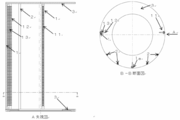
- FIG. 2 is a schematic view showing an example of a substrate holder suitably used in an embodiment of the present invention, and a cross-sectional view showing a cross section AA.
- A It is a figure for demonstrating the difference of the distance of the conventional substrate holder and a wafer edge part, and the distance of the substrate holder of this invention, and a wafer edge part.
- A It is a general-view figure which shows one Example of the mounting part attached to the support
- B is a cross-sectional view showing an example of a mounting portion attached to a column of a substrate holder preferably used in an embodiment of the present invention. It is sectional drawing which shows the positional relationship of the support
- FIG. 6 is a side view showing another example of a substrate holder suitably used in the embodiment of the present invention and a cross-sectional view showing a BB cross section.
- FIG. 1 and 2 show a substrate processing apparatus 10 preferably used in an embodiment of the present invention.
- the substrate processing apparatus 10 is configured as an example of a semiconductor manufacturing apparatus used for manufacturing a semiconductor device (device).
- the processing furnace 202 is provided with a heater 207 as a heating unit for heating the wafer (substrate) 200.
- a reaction tube 203 constituting a reaction vessel (processing vessel) concentrically with the heater 207 is disposed.
- the reaction tube 203 is made of a heat-resistant material such as quartz (SiO 2 ), and is formed in a cylindrical shape having a closed upper end and an opened lower end.
- a manifold 209 made of, for example, stainless steel is attached to the lower end of the reaction tube 203.
- the manifold 209 is formed in a cylindrical shape, and its lower end opening is airtightly closed by a seal cap 219 that is a lid.
- O-rings 220 are provided between the reaction tube 203, the manifold 209, and the seal cap 219, respectively.
- the reaction chamber 203, the manifold 209, and the seal cap 219 form a processing chamber 201.
- a boat 217 as a substrate holding unit is erected on the seal cap 219 via a boat support base 218.
- a plurality of wafers 200 to be batch-processed are stacked in a horizontal posture in multiple stages in the vertical direction.
- the boat 217 can be moved up and down with respect to the reaction tube 203 by the boat elevator 115.
- a boat rotation mechanism 267 that rotates the boat 217 is provided at the lower end of the boat support 218 in order to improve processing uniformity.
- the heater 207 heats the wafer 200 inserted into the processing chamber 201 to a predetermined temperature.
- a nozzle 410 (first nozzle 410), a nozzle 420 (second nozzle 420), and a nozzle 430 (third nozzle 430) are provided so as to penetrate the lower part of the reaction tube 203.
- the nozzle 410, the nozzle 420, and the nozzle 430 include a gas supply pipe 310 (first gas supply pipe 310), a gas supply pipe 320 (second gas supply pipe 320), and a gas supply pipe 330 (first gas supply line) as gas supply lines. 3 gas supply pipes 330) are connected to each other.
- the reaction tube 203 is provided with the three nozzles 410, 420, and 430 and the three gas supply tubes 310, 320, and 330.
- the gas (processing gas) can be supplied.
- the gas supply pipe 310 is provided with a mass flow controller (abbreviation: MFC) 312 which is a flow rate control device (flow rate control unit) and a valve 314 which is an on-off valve in order from the upstream side.
- MFC mass flow controller
- a nozzle 410 is connected to the tip of the gas supply pipe 310.
- the nozzle 410 is configured as an L-shaped long nozzle, and its horizontal portion is provided so as to penetrate the side wall of the manifold 209. The vertical portion of the nozzle 410 rises upward (in the loading direction of the wafer 200) along the inner wall of the reaction tube 203 in an arc-shaped space formed between the inner wall of the reaction tube 203 and the wafer 200.
- the nozzle 410 is provided on the side of the wafer arrangement area where the wafers 200 are arranged, in a region that horizontally surrounds the wafer arrangement area, along the wafer arrangement area.
- a gas supply hole 410 a for supplying gas is provided on the side surface of the nozzle 410.
- the gas supply hole 410 a is opened to face the center of the reaction tube 203.
- a plurality of the gas supply holes 410a are provided from the lower part to the upper part of the reaction tube 203, have the same or inclined opening areas, and are provided at the same opening pitch.
- the first gas supply system is mainly configured by the gas supply pipe 310, the MFC 312, the valve 314, and the nozzle 410.
- a carrier gas supply pipe 510 for supplying a carrier gas is connected to the gas supply pipe 310.
- a carrier gas supply pipe 510, MFC 512, and valve 514 mainly constitute a first carrier gas supply system.
- the gas supply pipe 320 is provided with an MFC 322 as a flow rate control device (flow rate control unit) and a valve 324 as an on-off valve in order from the upstream side.
- a nozzle 420 is connected to the tip of the gas supply pipe 320.
- the nozzle 420 is configured as an L-shaped long nozzle similar to the nozzle 410.
- the configuration of the horizontal portion and the vertical portion of the nozzle 420 is the same as that of the nozzle 410.
- a gas supply hole 420 a for supplying gas is provided on the side surface of the nozzle 420.
- the gas supply hole 420a has the same configuration as the gas supply hole 410a.
- a second gas supply system is mainly configured by the gas supply pipe 320, the MFC 322, the valve 324, and the nozzle 420.
- a carrier gas supply pipe 520 for supplying a carrier gas is connected to the gas supply pipe 320.
- the carrier gas supply pipe 520, MFC 522, and valve 524 mainly constitute a second carrier gas supply system.
- the gas supply pipe 330 is provided with an MFC 332 as a flow rate control device (flow rate control unit) and a valve 334 as an on-off valve in order from the upstream side.
- a nozzle 430 is connected to the tip of the gas supply pipe 330.
- the nozzle 430 is configured as an L-shaped long nozzle. The configuration of the horizontal portion and the vertical portion of the nozzle 430 is the same as that of the nozzles 410 and 420.
- a gas supply hole 430 a for supplying gas is provided on the side surface of the nozzle 430.
- the gas supply hole 430a is provided with the same configuration as the gas supply holes 410a and 420a.
- the third gas supply system is mainly configured by the gas supply pipe 330, the MFC 332, the valve 334, and the nozzle 430.
- a carrier gas supply pipe 530 for supplying a carrier gas is connected to the gas supply pipe 330.
- a third carrier gas supply system is mainly configured by the carrier gas supply pipe 530, the MFC 532, and the valve 534.
- the gas supply method includes a nozzle 410 arranged in an arc-like vertically long space defined by the inner wall of the reaction tube 203 and the ends of a plurality of stacked wafers 200,
- the gas is conveyed through 420 and 430, and the gas is jetted into the reaction tube 203 for the first time in the vicinity of the wafer 200 from the gas supply holes 410a, 420b and 430c opened in the nozzles 410, 420 and 430, respectively.
- the main flow of gas in the reaction tube 203 is set in a direction parallel to the surface of the wafer 200, that is, in a horizontal direction.
- the residual gas after the reaction flows toward the exhaust port, that is, the direction of the exhaust pipe 231 described later.
- the direction of the residual gas flow is appropriately specified by the position of the exhaust port and is limited to the vertical direction. It is not a thing.
- titanium tetrachloride which is a Ti-containing raw material containing at least titanium (Ti) element
- TiCl 4 titanium tetrachloride
- 314 is supplied into the processing chamber 201 through the nozzle 410.
- a liquid material that is in a liquid state at normal temperature and pressure such as TiCl 4
- the liquid material is vaporized by a vaporization system such as a vaporizer or bubbler and supplied as TiCl 4 gas that is a Ti-containing gas. It becomes.
- TMA trimethylaluminum. (CH 3 ) 3 Al) containing at least a carbon (C) element and an aluminum (Al) element.
- C carbon
- Al aluminum
- TMA trimethylaluminum.
- a liquid raw material will be vaporized by vaporization systems, such as a vaporizer and a bubbler, and will be supplied as C and Al containing gas.
- ammonia (NH 3 ) is supplied into the processing chamber 201 through the MFC 332, the valve 334, and the nozzle 430 as a source gas containing nitrogen element.
- nitrogen (N 2 ) gas is supplied into the processing chamber 201 through MFCs 512, 522 and 532, valves 514, 524 and 534, and nozzles 410, 420 and 430, respectively. Is done.
- the first gas supply system constitutes a metal-containing raw material supply system.
- the second gas supply system constitutes a carbon-containing raw material supply system.
- a nitrogen-containing raw material supply system is configured by the third gas supply system.
- the second gas supply system may constitute a metal-containing raw material supply system in the same manner as the first gas supply system, and may constitute a nitrogen-containing raw material supply system as in the third gas supply system. May be.
- the reaction tube 203 is provided with an exhaust pipe 231 for exhausting the atmosphere in the processing chamber 201.
- the exhaust pipe 231 is provided at a position facing the nozzles 410, 420, and 430 in the manifold 209 so as to penetrate the side wall of the manifold 209.
- the exhaust pipe 231 includes, in order from the upstream side, a pressure sensor 245 as a pressure detector (pressure detector) for detecting the pressure in the processing chamber 201, an APC (Auto Pressure Controller) valve 243, and a vacuum pump as a vacuum exhaust device. 246 is connected.
- the APC valve 243 is an exhaust valve and functions as a pressure adjustment unit.
- An exhaust system, that is, an exhaust line, is mainly configured by the exhaust pipe 231, the APC valve 243, and the pressure sensor 245. Note that the vacuum pump 246 may be included in the exhaust system.
- the APC valve 243 is configured to be able to adjust the pressure in the processing chamber 201 by adjusting the valve opening while the vacuum pump 246 is operated.
- a temperature sensor 263 as a temperature detector is installed in the reaction tube 203, and the temperature in the processing chamber 201 is adjusted by adjusting the energization amount to the heater 207 based on the temperature information detected by the temperature sensor 263. It is configured to have a desired temperature distribution.
- the temperature sensor 263 is configured in an L shape similarly to the nozzles 410, 420, and 430, and is provided along the inner wall of the reaction tube 203.
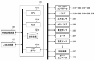
- the controller 121 is configured as a computer including a CPU (Central Processing Unit) 121a, a RAM (Random Access Memory) 121b, a storage device 121c, and an I / O port 121d.
- the RAM 121b, the storage device 121c, and the I / O port 121d are configured to exchange data with the CPU 121a via an internal bus.
- an input / output device 122 configured as a touch panel or the like is connected to the controller 121.
- the storage device 121c includes, for example, a flash memory, an HDD (Hard Disk Drive), and the like.
- a control program that controls the operation of the substrate processing apparatus, a process recipe that describes the procedure and conditions of the substrate processing described later, and the like are stored in a readable manner.
- the process recipe is a combination of functions so that a predetermined result can be obtained by causing the controller 121 to execute each procedure in a substrate processing step to be described later, and functions as a program.
- the process recipe, the control program, and the like may be collectively referred to simply as a program.
- the RAM 121b is configured as a memory area (work area) in which programs, data, and the like read by the CPU 121a are temporarily stored.
- the I / O port 121d includes the above-described MFC 312, 322, 332, 512, 522, 532, valves 314, 324, 334, 514, 524, 534, APC valve 243, pressure sensor 245, vacuum pump 246, heater 207, temperature The sensor 263, the rotation mechanism 267, the boat elevator 115 and the like are connected.
- the CPU 121a is configured to read out and execute a control program from the storage device 121c, and to read out a process recipe from the storage device 121c in response to an operation command input from the input / output device 122 or the like. Then, according to the read process recipe, the CPU 121a adjusts the flow rates of various gases by the MFCs 312, 322, 332, 512, 522, 532, the opening / closing operations of the valves 314, 324, 334, 514, 524, 534, and the APC valve 243.
- the boat elevator 115 is configured to control the lifting and lowering operation of the boat 217 and the like.
- the controller 121 is not limited to being configured as a dedicated computer, but may be configured as a general-purpose computer.
- the controller 121 according to the present embodiment is configured by installing the program in a general-purpose computer using an external storage device 123 (for example, a semiconductor memory such as a USB memory or a memory card) that stores the above-described program. be able to.
- the means for supplying the program to the computer is not limited to supplying the program via the external storage device 123.
- the program may be supplied without using the external storage device 123 by using communication means such as the Internet or a dedicated line.
- the storage device 121c and the external storage device 123 are configured as computer-readable recording media. Hereinafter, these are collectively referred to simply as a recording medium. Note that when the term “recording medium” is used in this specification, it may include only the storage device 121c alone, may include only the external storage device 123 alone, or may include both.
- the metal film forming step is performed as one step of the semiconductor device manufacturing process using the processing furnace 202 of the substrate processing apparatus 10 described above.
- substrate in this specification is the same as the term “wafer”. In that case, in the above description, “wafer” is replaced with “substrate”. Good.
- metal film means a film made of a conductive substance containing a metal atom, and includes a conductive metal nitride film, a conductive metal oxide film, and a conductive film.
- Metal oxynitride film, conductive metal composite film, conductive metal alloy film, conductive metal silicide film, conductive metal carbide film (metal carbide film), conductive metal carbonitride film (metal carbonitride film) ) Etc. are included.
- FIG. 4 is a process flow diagram showing an example of a process for forming a metal film (TiN film).
- the operation of each part constituting the substrate processing apparatus 10 is controlled by the controller 121.
- the inside of the processing chamber 201 is evacuated by the vacuum pump 246 so that a desired pressure (degree of vacuum) is obtained. At this time, the pressure in the processing chamber 201 is measured by the pressure sensor 245, and the APC valve 243 is feedback-controlled based on the measured pressure information (pressure adjustment). Further, the processing chamber 201 is heated by the heater 207 so as to have a desired temperature. At this time, the energization amount to the heater 207 is feedback-controlled based on the temperature information detected by the temperature sensor 263 so that the processing chamber 201 has a desired temperature distribution (temperature adjustment). Subsequently, the rotation mechanism 267 starts the rotation of the boat 217 and the wafer 200.
- the vacuum pump 246 is always operated until at least the processing on the wafer 200 is completed, and the heating in the processing chamber 201 by the heater 207 and the rotation of the boat 217 and the wafer 200 by the rotation mechanism 267 are continued. Done.
- Step 11 a process of forming a TiN layer (Step 11 to Step 14) is performed.
- Step 11> TiCl 4 Gas Supply
- the valve 314 of the gas supply pipe 310 is opened, and TiCl 4 gas as the first raw material is caused to flow in the gas supply pipe 310.
- the flow rate of the TiCl 4 gas that has flowed through the gas supply pipe 310 is adjusted by the MFC 312.
- the flow-adjusted TiCl 4 gas is supplied into the processing chamber 201 from the gas supply hole 410 a of the nozzle 410 and is exhausted from the exhaust pipe 231. At this time, TiCl 4 gas is supplied to the wafer 200.
- the valve 514 is opened, and an inert gas such as N 2 gas is allowed to flow into the carrier gas supply pipe 510.
- the flow rate of the N 2 gas that has flowed through the carrier gas supply pipe 510 is adjusted by the MFC 512.
- the N 2 gas whose flow rate has been adjusted is supplied into the processing chamber 201 together with the TiCl 4 gas, and is exhausted from the exhaust pipe 231.
- the valves 524 and 534 are opened, and N 2 gas is allowed to flow into the carrier gas supply pipe 520 and the carrier gas supply pipe 530.
- the N 2 gas is supplied into the processing chamber 201 through the gas supply pipe 320, the gas supply pipe 330, the nozzle 420, and the nozzle 430 and is exhausted from the exhaust pipe 231.
- the APC valve 243 is appropriately adjusted so that the pressure in the processing chamber 201 is, for example, in the range of 1 to 10,000 Pa.
- the supply flow rate of TiCl 4 gas controlled by the MFC 312 is, for example, a flow rate in the range of 10 to 10,000 sccm.
- the supply flow rate of N 2 gas controlled by the MFCs 512, 522, and 532 is set to a flow rate within a range of 10 to 10,000 sccm, for example.
- the time for supplying the TiCl 4 gas to the wafer 200, that is, the gas supply time (irradiation time) is, for example, a time within the range of 0.1 to 120 seconds.
- the temperature of the heater 207 is set to such a temperature that the temperature of the wafer 200 becomes a temperature within a range of 200 to 500 ° C., for example.
- a Ti-containing layer having a thickness of, for example, less than one atomic layer to several atomic layers is formed on the wafer 200.
- Step 12> (Residual Gas Removal) After the Ti-containing layer is formed, the valve 314 of the gas supply pipe 310 is closed, and the supply of TiCl 4 gas is stopped. At this time, the APC valve 243 of the exhaust pipe 231 is kept open, the inside of the processing chamber 201 is evacuated by the vacuum pump 246, and TiCl 4 after remaining in the processing chamber 201 or contributing to the formation of the Ti-containing layer. The gas is removed from the processing chamber 201. At this time, the valves 514, 524, and 534 are kept open, and the supply of N 2 gas into the processing chamber 201 is maintained. The N 2 gas acts as a purge gas, which can enhance the effect of removing the unreacted or residual TiCl 4 gas that has contributed to the formation of the Ti-containing layer from the processing chamber 201.
- Step 13> (NH 3 Gas Supply) After removing the residual gas in the processing chamber 201, the valve 334 of the gas supply pipe 330 is opened, and NH 3 gas is caused to flow into the gas supply pipe 330. The flow rate of NH 3 gas that has flowed through the gas supply pipe 330 is adjusted by the MFC 332. The NH 3 gas whose flow rate has been adjusted is supplied into the processing chamber 201 from the gas supply hole 430 a of the nozzle 430. The NH 3 gas supplied into the processing chamber 201 is activated by heat and then exhausted from the exhaust pipe 231. At this time, NH 3 gas activated by heat is supplied to the wafer 200.
- the valve 534 is opened, and N 2 gas is caused to flow into the carrier gas supply pipe 530.
- the flow rate of the N 2 gas flowing through the carrier gas supply pipe 530 is adjusted by the MFC 532.
- the N 2 gas is supplied into the processing chamber 201 together with the NH 3 gas, and is exhausted from the exhaust pipe 231.
- the valves 514 and 524 are opened, and the N 2 gas is allowed to flow into the carrier gas supply pipes 510 and 520.
- the N 2 gas is supplied into the processing chamber 201 through the gas supply pipes 310 and 320, the nozzle 410 and the nozzle 420, and is exhausted from the exhaust pipe 231.
- the APC valve 243 is appropriately adjusted so that the pressure in the processing chamber 201 is, for example, in the range of 1 to 10,000 Pa.
- the supply flow rate of NH 3 gas controlled by the MFC 332 is set to a flow rate in the range of 10 to 50000 sccm, for example.
- the supply flow rate of N 2 gas controlled by the MFCs 512, 522, and 532 is set to a flow rate within a range of 10 to 10,000 sccm, for example.
- the time for supplying the NH 3 gas activated by heat to the wafer 200, that is, the gas supply time (irradiation time) is, for example, a time within the range of 0.1 to 120 seconds.
- the temperature of the heater 207 at this time is set to such a temperature that the temperature of the wafer 200 becomes a temperature in the range of 200 to 500 ° C., for example, as in step 11.
- the gas flowing into the processing chamber 201 is NH 3 gas that is thermally activated by increasing the pressure in the processing chamber 201, and this activated NH 3 gas is converted into the wafer in step 11. Reacts with at least a portion of the Ti-containing layer formed on 200. As a result, the Ti-containing layer is nitrided and modified into a titanium nitride layer (TiN layer).
- Step 14> (Residual gas removal)
- the valve 334 of the gas supply pipe 330 is closed to stop the supply of NH 3 gas.
- the APC valve 243 of the exhaust pipe 231 is kept open, the inside of the processing chamber 201 is evacuated by the vacuum pump 246, and the NH 3 gas remaining in the processing chamber 201 and contributing to the formation of the TiN layer remains.
- reaction by-products are removed from the processing chamber 201.
- the valves 514, 524, and 534 are kept open, and the supply of N 2 gas into the processing chamber 201 is maintained.
- the N 2 gas acts as a purge gas, thereby enhancing the effect of removing NH 3 gas and reaction by-products remaining in the processing chamber 201 and contributing to formation of the TiN layer from the processing chamber 201. Can do.
- step 11 to step 14 is executed X times (first predetermined number of times) set in advance. That is, the process from step 11 to step 14 is set as one set, and these processes are executed for X sets.
- TiTi 4 gas supply and NH 3 gas supply are alternately performed X times to form a TiN layer (first layer) having a predetermined thickness (for example, 0.03 to 20 nm).
- the seal cap 219 is lowered by the boat elevator 115 to open the lower end of the reaction tube 203 and the processed wafer 200 is supported by the boat 217 in the state where the reaction tube 203 is supported. It is carried out of the reaction tube 203 from the lower end. Thereafter, the processed wafer 200 is taken out from the boat 217.
- the distance between the end of the wafer 200 and the column 100 is insufficient, and the gas consumption by the column 100 is reduced.
- the uniformity of the film thickness on the surface of the wafer 200 cannot be secured.
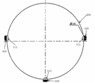
- the boat 217 in the present embodiment shown in FIG. 6 is provided on each outer periphery of the top plate 3 and the bottom plate 4, and is provided on each outer periphery of the column 1 holding the wafer 200, and each of the top plate 3 and the bottom plate 4.
- the auxiliary strut 2 has a smaller diameter than the strut 1.
- the support column 1 is provided with support pins (hereinafter also referred to as a mounting tool) 11 as a mounting portion on which the wafer 200 is mounted. When the wafer 200 is placed on the placement unit 11, the end of the wafer 200 and the support column 1 are separated from each other by a predetermined length.
- the support column 1 and the auxiliary support column 2 are provided on the outer periphery of the top plate 3 and the bottom plate 4, respectively, by reducing the diameters of the support column 1 and the auxiliary support column 2, respectively, The distance between the end of 200 and each of the support column 1 and the auxiliary support column 2 can be separated.
- the diameter of the support column 1 is such that the wafer 200 is supported by the mounted mounting unit 11 while maintaining the strength with which the wafer 200 can be mounted on the mounted mounting unit 11.
- the distance from the end is configured to be a predetermined length.
- the mounting unit 11 includes a contact unit 12 that comes into contact with the wafer 200 and a main body unit 13 that forms a space between the support column 1 and the contact unit 12. For example, it is preferable to provide a step at the boundary between the contact portion 12 and the main body portion 13. Due to such a configuration, when the wafer 200 is held on the mounting portion 11 (or the contact portion 12), the distance between the end portion of the wafer 200 and the surface of the support column 1 is approximately the same as that of the main body portion 13. Is done. Accordingly, the length of the main body 13 is determined so that the predetermined length becomes an optimum value. Moreover, the mounting part 11 (contact part 12, the main-body part 13) is cylindrical shape, and a cross section is a circle.
- the mounting portion 11 attached to the boat 217 according to the present invention has at least a main body portion 13 attached to a groove of the boat 217 and a contact portion 12 on which the wafer 200 is placed. It is a configuration.
- the contact portion 12 and the main body portion 13 are provided with a step so that the wafer 200 can be positioned. Further, because of such a configuration, the predetermined length from the support column 1 to the end of the wafer 200 can be changed by changing the length of the main body 13. That is, the main body is configured to be appropriately selected according to the diameter of the support column 1 and the diameter of the wafer 200. Thus, the support pin (mounting tool) 11 is configured by the contact portion 12 and the main body portion 13.
- pillar 2 is provided in the position which divides
- the boat 217 is configured to be equidistant between the support column 1 and the auxiliary support column 2 or between the auxiliary support columns 2 in the circumferential direction.
- the boat 217 includes a plurality of support columns 1, a reference support column 1 a is provided in the direction in which the wafer 200 is placed, and the support column 1 is attached to the wafer 200 around the reference support column 1 a. It is configured to be provided at a position that is symmetrical with respect to the mounting direction.
- the strut 1 and the auxiliary strut 2 in the boat 217 are left and right with respect to the direction in which the wafer 200 is placed with the reference strut 1a as the center. It is provided at a symmetrical position.
- pillar 2 is smaller than the diameter of the support
- three struts 1 and four auxiliary struts 2 are equally provided between the struts 1 and the auxiliary struts 2 or between the auxiliary struts 2 in the circumferential direction of the wafer 200.
- the present invention is not limited to this form, and various configurations are conceivable as shown in FIG.
- the column 1 of the boat 217 of the present invention is configured to be thinner than the column 1 of the conventional boat 217, several are attached for the purpose of ensuring strength.
- the diameter of the pillar 1 of the conventional boat 217 shown in FIG. 5 is 19 mm
- the diameter of the pillar 1 of the boat 217 of the present invention shown in FIG. 6 is 13 mm
- the diameter of the auxiliary pillar 2 is 10 mm.
- the diameter ( ⁇ 13 mm) of the column 1 of the boat 217 of the present invention shown in FIG. 6 is 6 mm thinner than the diameter ( ⁇ 19 mm) of the column 100 of the conventional boat 217 shown in FIG.
- the distance from the support column 1 to the end of the wafer 200 can be maintained at least twice (5 mm or more).
- the diameter of the support column 1 is set in advance so as to have a strength capable of mounting the wafer 200 on the mounting unit 11. Therefore, the diameter ( ⁇ 13 mm) of the support 1 in this embodiment is an example, and the present embodiment also includes a case where the diameter having a strength capable of mounting the wafer 200 is 10 mm or less due to the material of the diameter of the support 1. included.
- the auxiliary strut 2 is preferably as small as possible because the supporting strut 2 is not required to have a strength that can be supported by the wafer 200 by providing the mounting portion 11.
- the diameter is too small, the deformation due to heat becomes remarkable, so ⁇ 8 mm or more is preferable.
- the boat 217 of the present invention shown in FIG. 6 has a configuration including a separating plate 5 that separates a substrate processing region which is a region for holding a substrate and a heat insulating region which is a region for holding a heat insulating plate. Grooves are engraved on the entire support column 1 from the substrate processing region to the heat insulation region, and a mounting portion 11 is attached to the groove of the support column 1 in the substrate processing region. Even in the groove of the support 1, a groove for placing the heat insulating plate is formed in the heat insulating region.
- the auxiliary support column 2 is not engraved with a groove throughout, so that the wafer 200 and the heat insulating plate cannot be placed.
- the boat 217 shown in FIG. 13 has a configuration excluding the heat insulating region of the boat 217 in the present embodiment, and the other configurations are the same. That is, this boat 217 also has the same effect as the boat 217 in this embodiment shown in FIG.
- the diameter of the auxiliary column 2 is smaller than the diameter of the column 1, and when the wafer 200 is held by the mounting unit 11, the distance between the end of the wafer 200 and the surface of the column 1. Are separated by a predetermined length.
- the support column 1 of the boat 207 is configured to be thin enough to hold the wafer 200 by the mounting unit 11, and by appropriately selecting the length of the main body 13 of the mounting unit 11, A predetermined length between the end portion and the support column 1 can be freely determined.
- pillar 2 can be considered.
- the column 1 and the end of the wafer 200 need only have a predetermined length or more. For example, when the wafer 200 is held by the boat 217, if the distance between the column 1 and the end of the wafer 200 is sufficiently long, It is good also as a structure which enlarges the support
- FIG. 10 is a diagram for simply explaining a method of calculating the distance (predetermined length) between the boat 217 and the end of the wafer 200 (hereinafter also referred to as a wafer edge).
- a wafer edge a method of calculating the distance (predetermined length) between the boat 217 and the end of the wafer 200
- the distance (2 mm) between the current boat 217 and the wafer edge is 14 mm which is a difference of 3 mm from the sum of 15 mm.
- E / E Edge Exclusion
- a range excluded when measuring the film thickness of the wafer is 3 mm.
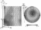
- FIG. 11 shows a film thickness measurement result obtained by forming a TiN film on the wafer 200 and measuring the film thickness.
- a temperature of 380 ° C., a TiCl 4 gas flow rate of 0.45 slm (carrier N 2 gas flow rate of 1.5 slm), and an NH 3 gas flow rate of 7.5 slm (carrier N 2 gas flow rate of 3.4 slm) are alternated for a predetermined pressure and a predetermined time
- the diameter ⁇ of the column of the boat 217 is 19 mm, and the pitch is 7.7 mm.
- the influence of the column 1 of the boat 217 was verified with the film thickness in the vicinity of the column 1 of the boat 217 (the portion surrounded by the square) in the overall view (enlarged view A) of the wafer 200 on the right side. . Since the verification method does not change in other parts, only the A part will be described here. Specifically, the influence on the film thickness of the column 1 of the boat 217 is verified using the enlarged view on the left side.
- the black dots shown in FIG. 11 are film thickness measurement points, and the portions having the same film thickness are indicated by solid lines.
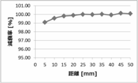
- the vertical axis indicates the attenuation factor
- the horizontal axis indicates the distance from the wafer edge.
- the attenuation rate reaches 99% is defined as a limit point at which the influence of the support column 1 can be ignored, it can be understood that the influence of the support column 1 can be ignored if it is 5 mm or more.
- the distance between the end portion of the substrate and the substrate holder is held so as to be equal to or longer than a predetermined length, so that it is affected by gas consumption by the substrate holder. Therefore, a decrease in film thickness uniformity can be suppressed.
- the predetermined length should just be 5 mm or more, 10 mm or more is preferable and 25 mm or more is still more preferable.
- the support of the substrate holder is provided with a mounting portion for holding the substrate, and by placing the substrate on the mounting portion, the support and the end of the substrate have a predetermined length ( 5 mm) or more. Since it is such a structure, the fall of the uniformity of a film thickness can be suppressed without being influenced by the gas consumption by a support
- the placement portion has a contact portion that supports the substrate and a main body portion that constitutes between the support column and the contact portion.
- the support portion and the end portion of the substrate Is configured to be the length of the main body. Therefore, by adjusting the length of the main body, the length of the support and the end of the substrate can be adjusted.
- the placement portion is configured such that a step is provided between the contact portion and the main body portion, and the substrate is placed on the contact portion. Accordingly, by adjusting the length of the main body, the length of the support and the end of the substrate can be adjusted. Moreover, it is preferable that the length of the contact portion is substantially the same as the length of E / E.
- a substrate holder provided with a support column to which a mounting unit for mounting a substrate is mounted is provided, and the diameter of the column can be mounted on the mounted mounting unit
- the distance from the end of the substrate is set to a predetermined length (5 mm or more). Accordingly, it is possible to suppress a decrease in film thickness uniformity without being affected by gas consumption by the substrate holder.
- the substrate holder is provided with the support column to which the mounting unit for mounting the substrate is mounted and the auxiliary column to which the mounting unit is not mounted.
- the end portion of the substrate and the support column are separated from each other by a predetermined length (5 mm or more). Accordingly, it is possible to suppress a decrease in film thickness uniformity without being affected by gas consumption by the substrate holder.
- the present invention is not limited to such an embodiment.
- the present invention can be suitably applied to a case where a film or the like formed on the wafer 200 is subjected to processes such as an oxidation process, a diffusion process, an annealing process, and an etching process.
- the present invention is not limited to this, and a cold wall type processing furnace is provided.
- the present invention can also be suitably applied when forming a thin film using a substrate processing apparatus.
- the present invention can be applied not only to a semiconductor manufacturing apparatus that processes a semiconductor wafer such as the substrate processing apparatus according to the present embodiment, but also to an LCD (Liquid Crystal Display) manufacturing apparatus that processes a glass substrate.
- a semiconductor manufacturing apparatus that processes a semiconductor wafer
- LCD Liquid Crystal Display
- a substrate in which a boat loaded with a substrate is loaded into a furnace, and a reaction gas is introduced from a reaction gas introduction pipe and processed into the substrate while the furnace is depressurized to a predetermined pressure and set to a predetermined temperature. Applies to processing equipment.
Landscapes
- Chemical & Material Sciences (AREA)
- General Chemical & Material Sciences (AREA)
- Chemical Kinetics & Catalysis (AREA)
- Engineering & Computer Science (AREA)
- Materials Engineering (AREA)
- Mechanical Engineering (AREA)
- Metallurgy (AREA)
- Organic Chemistry (AREA)
- Inorganic Chemistry (AREA)
- Chemical Vapour Deposition (AREA)
- Container, Conveyance, Adherence, Positioning, Of Wafer (AREA)
Abstract
Description
Claims (17)
- 基板を載置する載置部が取り付けられた支柱と前記載置部が取り付けられていない補助支柱を備えた基板保持具が設けられ、前記基板保持具は、前記補助支柱の径が前記支柱の径より小さく構成され、前記基板を前記載置部で保持する際、前記基板の端部と前記支柱の間が所定長さ離間するよう構成されている基板処理装置。
- 前記所定長さは、5mm以上である請求項1記載の基板処理装置。
- 前記支柱の径は、取り付けられた前記載置部に前記基板を載置可能な強度を保持するよう構成されている請求項1記載の基板処理装置。
- 前記載置部は、前記基板を支持する接触部と、前記接触部と前記支柱との間を構成する本体部がそれぞれ設けられ、前記基板保持具は、前記基板の端部と前記支柱の間を前記本体部の長さ離間させて、前記基板を前記接触部で保持するよう構成されている請求項1記載の基板処理装置。
- 前記載置部は、前記接触部と前記本体部との間に段差が設けられるよう構成されている請求項4記載の基板処理装置。
- 前記基板保持具は、複数の前記支柱及び前記補助支柱を有し、前記支柱の内、前記基板の載置される方向に基準支柱が設けられ、前記基準支柱を中心にして前記支柱及び補助支柱を前記基板の載置される方向に対して左右対称となる位置に設けられるよう構成されている請求項1記載の基板処理装置。
- 前記支柱と前記補助支柱は、前記支柱と前記補助支柱の間、及び前記補助支柱間を周方向に等間隔になるよう設けられている請求項6記載の基板処理装置。
- 基板を載置する載置部が取り付けられた支柱と前記載置部が取り付けられていない補助支柱を備えた基板保持具であって、前記補助支柱の径が前記支柱の径より小さく構成され、前記基板を前記載置部で保持する際、前記基板の端部と前記支柱の間が所定長さ離間するよう構成されている基板保持具。
- 基板を載置する載置部が取り付けられた支柱を備えた基板保持具が設けられ、前記支柱は、取り付けられた前記載置部に前記基板を載置可能な強度を保持するよう設定され、且つ、取り付けられた前記載置部で基板を支持させる際、前記基板の端部との距離が所定長さ設けられるよう構成されている基板処理装置。
- 基板を載置する載置部が取り付けられた支柱を備えた基板保持具であって、前記支柱は、取り付けられた前記載置部に前記基板を載置可能な強度を保持するよう設定され、且つ、取り付けられた前記載置部で基板を支持させる際、前記基板の端部との距離が所定長さ設けられるよう構成されている基板保持具。
- 基板を載置する載置部が取り付けられた支柱を備えた基板保持具であって、前記載置部は、前記基板を支持する接触部と、前記接触部と前記支柱との間を構成する本体部と、を有し、前記基板の端部と前記支柱の間を前記本体部の長さ離間させて、前記基板を前記接触部で保持するよう構成されている基板保持具。
- 前記載置部は、前記接触部と前記本体部との間に段差が設けられるよう構成されている請求項11記載の基板保持具。
- 更に、前記載置部が取り付けられていない補助支柱を有し、前記補助支柱の径は、前記の支柱の径より小さく構成されている請求項11記載の基板保持具。
- 更に、複数の前記支柱及び前記補助支柱を有し、複数の前記支柱のうち、前記基板の載置される方向に基準支柱が設けられ、前記基準支柱を中心にして前記支柱及び前記補助支柱を前記基板の載置される方向に対して左右対称となる位置に設けられるよう構成されている請求項11記載の基板保持具。
- 基板を載置する支柱に設けられ、前記基板を支持する接触部と、前記接触部と前記支柱との間を構成する本体部と、を含む載置具であって、前記基板を前記接触部で保持する際に、前記基板の端部と前記支柱の間を前記本体部の長さ離間させるよう構成されている載置具。
- 前記本体部は、前記支柱の径の大きさ、及び/又は、前記基板の径の大きさに応じて選択されるよう構成されている請求項15記載の載置具。
- 基板が載置される載置部が取付られた支柱を少なくとも備えた基板保持具を有し、前記載置部は、基板を支持する接触部と、前記接触部と前記支柱との間を構成する本体部がそれぞれ設けられ、前記基板保持具は、前記基板の端部と前記支柱の間を前記本体部の長さ離間させて、前記基板を前記接触部で保持するよう構成されている基板処理装置。
Priority Applications (4)
| Application Number | Priority Date | Filing Date | Title |
|---|---|---|---|
| KR1020187022564A KR102253522B1 (ko) | 2016-02-10 | 2016-09-26 | 기판 처리 장치, 기판 유지구, 적재구 및 반도체 장치의 제조 방법 |
| CN201680079936.5A CN109075069A (zh) | 2016-02-10 | 2016-09-26 | 衬底处理装置、衬底保持件及载置件 |
| JP2017566505A JP6560767B2 (ja) | 2016-02-10 | 2016-09-26 | 基板処理装置、基板保持具及び半導体装置の製造方法 |
| US16/100,384 US11031270B2 (en) | 2016-02-10 | 2018-08-10 | Substrate processing apparatus, substrate holder and mounting tool |
Applications Claiming Priority (2)
| Application Number | Priority Date | Filing Date | Title |
|---|---|---|---|
| JP2016-023625 | 2016-02-10 | ||
| JP2016023625 | 2016-02-10 |
Related Child Applications (1)
| Application Number | Title | Priority Date | Filing Date |
|---|---|---|---|
| US16/100,384 Continuation US11031270B2 (en) | 2016-02-10 | 2018-08-10 | Substrate processing apparatus, substrate holder and mounting tool |
Publications (1)
| Publication Number | Publication Date |
|---|---|
| WO2017138185A1 true WO2017138185A1 (ja) | 2017-08-17 |
Family
ID=59563227
Family Applications (1)
| Application Number | Title | Priority Date | Filing Date |
|---|---|---|---|
| PCT/JP2016/078220 Ceased WO2017138185A1 (ja) | 2016-02-10 | 2016-09-26 | 基板処理装置、基板保持具及び載置具 |
Country Status (5)
| Country | Link |
|---|---|
| US (1) | US11031270B2 (ja) |
| JP (1) | JP6560767B2 (ja) |
| KR (1) | KR102253522B1 (ja) |
| CN (1) | CN109075069A (ja) |
| WO (1) | WO2017138185A1 (ja) |
Cited By (1)
| Publication number | Priority date | Publication date | Assignee | Title |
|---|---|---|---|---|
| KR20210044849A (ko) | 2018-09-20 | 2021-04-23 | 가부시키가이샤 코쿠사이 엘렉트릭 | 기판 처리 장치, 반도체 장치의 제조 방법 및 프로그램 |
Families Citing this family (7)
| Publication number | Priority date | Publication date | Assignee | Title |
|---|---|---|---|---|
| JP6811147B2 (ja) * | 2017-06-23 | 2021-01-13 | 東京エレクトロン株式会社 | ガス供給系を検査する方法 |
| CN111433390B (zh) | 2017-12-22 | 2022-09-27 | 株式会社村田制作所 | 成膜装置 |
| CN111465714B (zh) * | 2017-12-22 | 2022-06-28 | 株式会社村田制作所 | 成膜装置 |
| KR102034766B1 (ko) * | 2018-04-12 | 2019-10-22 | 주식회사 유진테크 | 기판 처리 장치 및 기판 처리 방법 |
| WO2020175314A1 (ja) * | 2019-02-28 | 2020-09-03 | 株式会社Kokusai Electric | 半導体装置の製造方法、基板処理装置及びプログラム |
| CN113518836B (zh) * | 2019-03-06 | 2023-11-24 | 株式会社国际电气 | 半导体装置的制造方法、记录介质、基板处理装置和基板处理方法 |
| JP1651622S (ja) * | 2019-07-17 | 2020-01-27 |
Citations (2)
| Publication number | Priority date | Publication date | Assignee | Title |
|---|---|---|---|---|
| JPS6216516A (ja) * | 1985-07-15 | 1987-01-24 | Mitsubishi Electric Corp | 半導体製造装置 |
| JP2005228991A (ja) * | 2004-02-13 | 2005-08-25 | Hitachi Kokusai Electric Inc | 基板処理装置 |
Family Cites Families (15)
| Publication number | Priority date | Publication date | Assignee | Title |
|---|---|---|---|---|
| US5169453A (en) * | 1989-03-20 | 1992-12-08 | Toyoko Kagaku Co., Ltd. | Wafer supporting jig and a decompressed gas phase growth method using such a jig |
| US5458688A (en) * | 1993-03-09 | 1995-10-17 | Tokyo Electron Kabushiki Kaisha | Heat treatment boat |
| JP3672583B2 (ja) | 1993-07-22 | 2005-07-20 | 株式会社日立国際電気 | 半導体製造装置及び半導体製造方法 |
| JP3122364B2 (ja) * | 1996-02-06 | 2001-01-09 | 東京エレクトロン株式会社 | ウエハボート |
| JP3507624B2 (ja) * | 1996-06-28 | 2004-03-15 | 東京エレクトロン株式会社 | 熱処理用ボ−ト及び熱処理装置 |
| TWI250604B (en) * | 1999-07-29 | 2006-03-01 | Ibm | Improved ladder boat for supporting wafers |
| JP3167301B1 (ja) * | 1999-12-29 | 2001-05-21 | 株式会社半導体先端テクノロジーズ | ウェーハボートおよびウェーハボートを用いた熱処理装置 |
| JPWO2004003995A1 (ja) * | 2002-06-27 | 2005-11-04 | 株式会社日立国際電気 | 基板処理装置および半導体装置の製造方法 |
| KR100891259B1 (ko) * | 2003-11-27 | 2009-04-01 | 가부시키가이샤 히다치 고쿠사이 덴키 | 기판 처리 장치, 기판 보관 유지 장비, 및 반도체 장치의 제조 방법 |
| KR100557857B1 (ko) * | 2004-06-04 | 2006-03-10 | 주식회사 테라세미콘 | 반도체 제조장치의 웨이퍼 보트 |
| JP2006165134A (ja) * | 2004-12-03 | 2006-06-22 | Hitachi Kokusai Electric Inc | 基板処理装置 |
| US7661544B2 (en) * | 2007-02-01 | 2010-02-16 | Tokyo Electron Limited | Semiconductor wafer boat for batch processing |
| JP2014103280A (ja) * | 2012-11-20 | 2014-06-05 | Tokyo Electron Ltd | 保温体構造、基板保持ボート、処理装置及び処理システム |
| JP6054213B2 (ja) * | 2013-03-11 | 2016-12-27 | 東京エレクトロン株式会社 | 支持部材及び半導体製造装置 |
| JP6469046B2 (ja) * | 2016-07-15 | 2019-02-13 | クアーズテック株式会社 | 縦型ウエハボート |
-
2016
- 2016-09-26 JP JP2017566505A patent/JP6560767B2/ja active Active
- 2016-09-26 WO PCT/JP2016/078220 patent/WO2017138185A1/ja not_active Ceased
- 2016-09-26 CN CN201680079936.5A patent/CN109075069A/zh active Pending
- 2016-09-26 KR KR1020187022564A patent/KR102253522B1/ko active Active
-
2018
- 2018-08-10 US US16/100,384 patent/US11031270B2/en active Active
Patent Citations (2)
| Publication number | Priority date | Publication date | Assignee | Title |
|---|---|---|---|---|
| JPS6216516A (ja) * | 1985-07-15 | 1987-01-24 | Mitsubishi Electric Corp | 半導体製造装置 |
| JP2005228991A (ja) * | 2004-02-13 | 2005-08-25 | Hitachi Kokusai Electric Inc | 基板処理装置 |
Cited By (3)
| Publication number | Priority date | Publication date | Assignee | Title |
|---|---|---|---|---|
| KR20210044849A (ko) | 2018-09-20 | 2021-04-23 | 가부시키가이샤 코쿠사이 엘렉트릭 | 기판 처리 장치, 반도체 장치의 제조 방법 및 프로그램 |
| US11898247B2 (en) | 2018-09-20 | 2024-02-13 | Kokusai Electric Corporation | Substrate processing apparatus, method of manufacturing semiconductor device and non-transitory computer-readable recording medium |
| KR20240056777A (ko) | 2018-09-20 | 2024-04-30 | 가부시키가이샤 코쿠사이 엘렉트릭 | 기판 처리 장치, 반도체 장치의 제조 방법, 프로그램 및 기판 처리 방법 |
Also Published As
| Publication number | Publication date |
|---|---|
| CN109075069A (zh) | 2018-12-21 |
| JPWO2017138185A1 (ja) | 2018-11-22 |
| US11031270B2 (en) | 2021-06-08 |
| KR102253522B1 (ko) | 2021-05-18 |
| JP6560767B2 (ja) | 2019-08-14 |
| KR20180100632A (ko) | 2018-09-11 |
| US20180374734A1 (en) | 2018-12-27 |
Similar Documents
| Publication | Publication Date | Title |
|---|---|---|
| JP6560767B2 (ja) | 基板処理装置、基板保持具及び半導体装置の製造方法 | |
| TWI693381B (zh) | 溫度感測器、基板處理裝置及半導體裝置之製造方法 | |
| TWI668810B (zh) | 半導體裝置之製造方法、基板裝填方法及記錄媒體 | |
| JPWO2015041376A1 (ja) | 基板処理装置、半導体装置の製造方法および反応管 | |
| JP6647260B2 (ja) | 半導体装置の製造方法、基板処理装置及びプログラム | |
| KR102880793B1 (ko) | 기판 처리 방법, 기판 처리 장치, 프로그램 및 반도체 장치의 제조 방법 | |
| JP7539481B2 (ja) | 基板処理方法、プログラム及び基板処理装置 | |
| JP2018078323A (ja) | 基板処理装置 | |
| CN114941130A (zh) | 基板处理装置、基板处理方法、半导体装置的制造方法和存储介质 | |
| CN108695138A (zh) | 衬底支承件、衬底处理装置及半导体器件的制造方法 | |
| JP7539480B2 (ja) | 基板処理方法、プログラム、基板処理装置及び半導体装置の製造方法 | |
| JP7558287B2 (ja) | 基板処理方法、プログラム、基板処理装置及び半導体装置の製造方法 | |
| JP6753881B2 (ja) | 基板支持具、基板処理装置、及び半導体装置の製造方法 | |
| JP2011071412A (ja) | 基板処理装置 | |
| JP7844697B2 (ja) | 基板処理方法、半導体装置の製造方法、基板処理装置およびプログラム | |
| KR20200107762A (ko) | 기판 처리 장치, 반도체 장치의 제조 방법 및 기록 매체 | |
| JP7329133B2 (ja) | 基板処理装置、半導体装置の製造方法及びプログラム | |
| KR102880791B1 (ko) | 가스 공급 시스템, 기판 처리 장치 및 반도체 장치의 제조 방법 | |
| KR20250029973A (ko) | 기판 처리 장치, 기판 지지구, 기판 처리 방법, 반도체 장치의 제조 방법 및 프로그램 | |
| KR20230136556A (ko) | 기판 처리 방법, 반도체 장치의 제조 방법, 프로그램 및 기판 처리 장치 | |
| KR20240167810A (ko) | 기판 처리 장치, 가스 공급 시스템, 기판 처리 방법, 반도체 장치의 제조 방법 및 프로그램 | |
| CN118435321A (zh) | 基板处理装置、基板处理方法、半导体装置的制造方法、程序及气体供给单元 |
Legal Events
| Date | Code | Title | Description |
|---|---|---|---|
| 121 | Ep: the epo has been informed by wipo that ep was designated in this application |
Ref document number: 16889886 Country of ref document: EP Kind code of ref document: A1 |
|
| WWE | Wipo information: entry into national phase |
Ref document number: 2017566505 Country of ref document: JP |
|
| ENP | Entry into the national phase |
Ref document number: 20187022564 Country of ref document: KR Kind code of ref document: A |
|
| WWE | Wipo information: entry into national phase |
Ref document number: 1020187022564 Country of ref document: KR |
|
| NENP | Non-entry into the national phase |
Ref country code: DE |
|
| 122 | Ep: pct application non-entry in european phase |
Ref document number: 16889886 Country of ref document: EP Kind code of ref document: A1 |