WO2017130601A1 - 電力変換装置 - Google Patents
電力変換装置 Download PDFInfo
- Publication number
- WO2017130601A1 WO2017130601A1 PCT/JP2016/087701 JP2016087701W WO2017130601A1 WO 2017130601 A1 WO2017130601 A1 WO 2017130601A1 JP 2016087701 W JP2016087701 W JP 2016087701W WO 2017130601 A1 WO2017130601 A1 WO 2017130601A1
- Authority
- WO
- WIPO (PCT)
- Prior art keywords
- circuit
- switch element
- winding
- snubber
- switch
- Prior art date
- Legal status (The legal status is an assumption and is not a legal conclusion. Google has not performed a legal analysis and makes no representation as to the accuracy of the status listed.)
- Ceased
Links
Images





Classifications
-
- H—ELECTRICITY
- H02—GENERATION; CONVERSION OR DISTRIBUTION OF ELECTRIC POWER
- H02M—APPARATUS FOR CONVERSION BETWEEN AC AND AC, BETWEEN AC AND DC, OR BETWEEN DC AND DC, AND FOR USE WITH MAINS OR SIMILAR POWER SUPPLY SYSTEMS; CONVERSION OF DC OR AC INPUT POWER INTO SURGE OUTPUT POWER; CONTROL OR REGULATION THEREOF
- H02M3/00—Conversion of DC power input into DC power output
- H02M3/22—Conversion of DC power input into DC power output with intermediate conversion into AC
- H02M3/24—Conversion of DC power input into DC power output with intermediate conversion into AC by static converters
- H02M3/28—Conversion of DC power input into DC power output with intermediate conversion into AC by static converters using discharge tubes with control electrode or semiconductor devices with control electrode to produce the intermediate AC
Definitions
- This invention relates to the power converter device provided with the snubber circuit.
- Patent Document 1 discloses a snubber circuit that suppresses spike voltage.
- the snubber circuit described in Patent Document 1 includes a series circuit of a diode and a capacitor provided on the secondary side of the transformer of the switching regulator, and a switch element that discharges the charging voltage of the capacitor.
- the snubber circuit charges the generated spike voltage to the capacitor and immediately turns on the switch element to discharge the charge voltage as part of the output voltage.
- the power conversion efficiency is improved by regenerating the spike voltage stored in the capacitor without being consumed by the snubber circuit.
- a switching regulator using a transformer for example, there is a DC-DC converter.
- a system that full-wave rectifies the current output from the transformer may be employed.
- a circuit system such as a full bridge, a half bridge, or a push-pull is adopted on the primary side of the transformer.
- a full-wave rectification method there are a bridge rectification method and an intermediate tap method, but depending on the required characteristics (for example, reduction of conduction loss), a method of full-wave rectifying the current output from the transformer by the intermediate tap method May be adopted.
- An example in which the intermediate tap method is employed is Patent Document 2 and the like.
- the snubber circuit described in Patent Document 1 and the DC-DC converter described in Patent Document 2 can prevent a decrease in power conversion efficiency.
- the snubber circuit described in Patent Document 1 is applied to the DC-DC converter described in Patent Document 2, the following problems occur.
- the voltage cycle on the secondary side is 1 ⁇ 2 of the switching cycle on the primary side.
- the switch element of the snubber circuit is turned on even during the ON period of the rectifying switch to be protected. Period occurs, and excessive power stress is applied to the snubber circuit. As a result, the snubber circuit may be damaged or overheating may occur.
- an object of the present invention is to provide a power conversion device including a snubber circuit and a center tap type rectifier circuit, in which the power stress of the snubber circuit connected to the rectifying switch element is suppressed. is there.
- the power conversion device includes a transformer having a primary winding to which an AC voltage is applied, a secondary winding including a first end, a second end, and a center tap, the first end, and the first end.
- a first switch element connected between the output section, a second switch element connected between the second end and the first output section, and between the center tap and the second output section.
- a snubber circuit having a connected choke coil, a third switch element and a capacitor connected in series, and connected in parallel to at least one of the first switch element and the second switch element; and the third switch element A control circuit for turning on and off, the control circuit having a series circuit of a transformer auxiliary winding magnetically coupled to the primary winding of the transformer and a coil coupling winding magnetically coupled to the choke coil. And said straight The circuit is connected between a control terminal of the third switch element and the first end of the secondary winding, and the center tap and the second of the secondary winding and the secondary winding.
- a winding ratio between one end of the winding portion between one end or the winding portion between the center tap and the second end and the transformer auxiliary winding is represented by N1: N2: N3,
- the third switch element is turned on only when the first switch element or the second switch element that is the rectifying switch element to be protected is turned off. Therefore, it is possible to suppress an excessive power stress from being applied to the snubber circuit, particularly the third switch element. Further, it is possible to reduce the spike voltage generated in the rectifying switch element to be protected by the snubber circuit while preventing the third switch element from being damaged.
- the series circuit further includes a second capacitor
- the power converter further includes a resistance element connected between the control terminal of the third switch element and the first end of the secondary winding.
- a differential circuit may be formed by the second capacitor and the resistance element.
- the ON period of the third switch element can be adjusted by the differentiation circuit. Thereby, it is possible to prevent the third switch element from being turned on during the on period of the first switch element or the second switch element provided with the snubber circuit. As a result, the discharge current from the capacitor during the ON period of the first switch element or the second switch element can be prevented.
- the power converter may include a diode having a cathode connected to the control terminal of the third switch element and an anode connected to a reference potential terminal of the third switch element.
- This configuration can prevent an excessive reverse voltage from being applied to the control terminal of the third switch element.
- the power converter includes: a fourth switch element connected between a control terminal of the third switch element and a reference potential terminal; and the fourth switch with a set time constant when the third switch element is turned on. And a time constant circuit for turning on the element, and the third switch element may be turned off when the fourth switch element is turned on.
- the present invention it is possible to prevent an excessive power stress from being applied to the snubber circuit even if a center tap type transformer is used. As a result, it is possible to suppress the snubber circuit from being damaged or causing overheating.
- FIG. 1 is a circuit diagram of the power conversion apparatus according to the first embodiment.
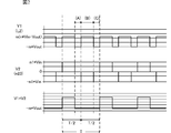
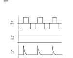
- FIG. 2 is a diagram illustrating waveforms of the voltage across the coil, the voltage across the auxiliary winding, and the total voltage thereof.
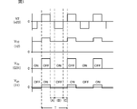
- FIG. 3 is a diagram illustrating waveforms of the voltage across the auxiliary winding, the charging voltage of the capacitor, the drain-source voltage of the switching element, and the gate voltage of the snubber switch.
- FIG. 4 is a circuit diagram of the power conversion apparatus according to the second embodiment.
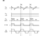
- FIG. 5 is a diagram showing waveforms of the gate voltage of the snubber switch, the charging voltage of the capacitor, the drain-source voltage of the switching element, the total voltage, and the voltage across the auxiliary winding.
- FIG. 6 is a circuit diagram of the power conversion apparatus according to the third embodiment.
- FIG. 7 is a diagram illustrating waveforms of the voltage across the auxiliary winding, the charging voltage of the capacitor, and the gate voltage of the snubber switch.
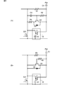
- FIG. 8A and FIG. 8B are diagrams illustrating a discharge circuit.
- 9A and 9B are diagrams illustrating a discharge circuit.
- FIG. 10 is a diagram showing waveforms of the voltage across the auxiliary winding, the charging voltage of the capacitor, and the gate voltage of the snubber switch.
- FIG. 11 is a circuit diagram of the power conversion apparatus according to the fifth embodiment.
- FIG. 1 is a circuit diagram of a power conversion device 1 according to the first embodiment.
- the power conversion device 1 is a DC-DC converter including a center tap rectifier circuit.
- the power conversion apparatus 1 includes input units IN1 and IN2 that input a DC voltage Vin and output units OUT1 and OUT2 that output a DC voltage Vout.
- the output unit OUT1 corresponds to a “first output unit” according to the present invention
- the output unit OUT2 corresponds to a “second output unit” according to the present invention.
- a switching circuit is connected to the input sections IN1 and IN2.
- the switching circuit is configured by connecting a series circuit of switching elements Q11 and Q12 and a series circuit of switching elements Q21 and Q22 in parallel.
- This switching circuit is switching-controlled by a driver (not shown), and switching elements Q11 and Q22 and switching elements Q12 and Q21 are alternately turned on and off.
- the switching elements Q11, Q12, Q21, and Q22 are MOSFETs, but may be elements having other structures such as IGBTs.
- the primary winding n11 of the transformer T1 is connected between the connection point of the switching elements Q11 and Q12 and the connection point of the switching elements Q21 and Q22.
- the secondary winding of the transformer T1 is configured by connecting a first winding n21 and a second winding n22 in series.
- a connection point P between the first winding n21 and the second winding n22 is a center tap of the secondary winding.
- connection point P is connected to the output part OUT2 via the choke coil L1.
- the choke coil L1 is a primary winding of the transformer T2.
- One end of the first winding n21 opposite to the connection point P (corresponding to the “first end” in the present invention) is connected to the output part OUT1 via the switching element Q31.
- One end of the second winding n22 opposite to the connection point P (corresponding to the “second end” in the present invention) is connected to the output part OUT1 via the switching element Q32.
- a smoothing capacitor Co is connected between the output parts OUT1 and OUT2.
- Switching elements Q31 and Q32 are MOSFETs. Switching element Q31 is turned on / off in synchronization with on / off of switching elements Q12, Q21. Switching element Q32 is turned on / off in synchronization with on / off of switching elements Q11, Q22.
- the switching element Q31 corresponds to a “first switch element” according to the present invention.
- the switching element Q32 corresponds to a “second switch element” according to the present invention.
- the power conversion device 1 When the switching elements Q11, Q22, and Q32 are on and the switching elements Q12, Q21, and Q31 are off (hereinafter, this state is referred to as a first state), the power conversion device 1 has a path indicated by a solid arrow shown in FIG. Current flows. When the switching elements Q11, Q22, and Q32 are off and the switching elements Q12, Q21, and Q31 are on (hereinafter, this state is referred to as a second state), the power conversion device 1 has a broken-line arrow shown in FIG. Current flows through the path.
- the snubber circuit 10 is connected in parallel to the switching element Q31.
- the snubber circuit 10 is a protection circuit that absorbs a spike voltage generated when the switching element Q31 is turned off and protects the switching element Q31 and surrounding components.
- the snubber circuit 10 is a series circuit of a snubber switch 11 and a capacitor 12.
- the snubber switch 11 is a MOSFET, the source of the snubber switch 11 is connected to the drain of the switching element Q31, and the drain of the snubber switch 11 is connected to the source of the switching element Q31 via the capacitor 12.
- the snubber switch 11 corresponds to a “third switch element” according to the present invention.
- a control circuit described later is connected to the gate (control terminal) of the snubber switch 11 and is turned on / off by the control circuit.
- the snubber switch 11 is turned on during the off period of the switching element Q31 and is turned off during the on period of the switching element Q31.
- the switching element Q31 is turned off, the voltage across the switching element Q31 rises rapidly. That is, a spike voltage is generated.
- the snubber switch 11 is turned on, the spike voltage is absorbed (charged) in the capacitor 12. As a result, the switching element Q31 and its peripheral components can be prevented from being damaged by the spike voltage.
- the control circuit is a series circuit of the coil L2 and the auxiliary winding n23. This series circuit is connected between the gate and source of the snubber switch 11.
- the control circuit in the present embodiment corresponds to a “control circuit” according to the present invention.
- the capacitor C1 is a capacitor for adjusting the voltage between the gate and the source of the snubber switch 11.
- the coil L2 is a secondary winding of the transformer T2, and is magnetically coupled to the choke coil L1 of the primary winding. In either case of the first state or the second state, the current flowing through the choke coil L1 is in the same direction. For this reason, the polarity of the voltage induced in the coil L2 magnetically coupled to the choke coil L1 is the same.
- the coil L2 corresponds to a “coil coupling winding” according to the present invention.
- the auxiliary winding n23 of the control circuit is magnetically coupled to the primary winding n11 of the transformer T1.
- An AC voltage is applied to the primary winding n11 by switching of the switching circuit.
- the polarity of the voltage induced in the auxiliary winding n23 is alternately inverted.
- the polarity of the voltage induced in the auxiliary winding n23 is the same as the polarity of the voltage induced in the coil L2.
- the polarity of the voltage induced in the auxiliary winding n23 is opposite to the polarity of the voltage induced in the coil L2.
- the auxiliary winding n23 corresponds to a “transformer auxiliary winding” according to the present invention.
- the control circuit outputs a total voltage (V1 + V2) of the voltage V1 induced in the coil L2 and the voltage V2 induced in the auxiliary winding n23. This total voltage (V1 + V2) is applied to the gate of the snubber switch 11.
- the total voltage (V1 + V2) output from the control circuit has a rectangular wave shape that turns on the snubber switch 11 when the switching element Q31 is off and turns off the snubber switch 11 when the switching element Q31 is on.
- Each element of the power converter 1 is set to a constant.
- the turns ratio of the primary winding n11, the first winding n21, and the auxiliary winding n23 is represented by N1: N2: N3, and the turns ratio of the choke coil L1 and the coil L2 is represented by N4: N5. .
- the snubber switch 11 is turned off when the switching element Q31 is turned on and turned on when the switching element Q31 is turned off. The reason will be described below.
- FIG. 2 is a diagram showing waveforms of the voltage V1 across the coil L2, the voltage V2 across the auxiliary winding n23, and the total voltage (V1 + V2) thereof.
- VL1 n * Vin ⁇ Vout.
- the repetition period of V2 is a switching period T.
- the total voltage (V1 + V2) is expressed by the following formula (1).
- the total voltage (V1 + V2) becomes the same potential as the total voltage (V1 + V2) in the periods (A) and (C). It becomes a pulse voltage.
- V1 + V2 ⁇ m * Vout. That is, the total voltage (V1 + V2) in the periods (A), (B), and (C) is ⁇ m * Vout, which is the same potential.
- the total voltage (V1 + V2) is applied to the gate of the snubber switch 11, so that the snubber switch 11 is turned on / off in a cycle T.
- the voltage output from the control circuit is only the voltage V1 across the coil L2.
- a voltage V 1 is applied to the gate of the snubber switch 11. Since the cycle of the voltage V1 is T / 2, the snubber switch 11 is turned on / off at a cycle of T / 2. Since the cycle of the switching element Q31 is T, the timing when the snubber switch 11 is turned on occurs when the switching element Q31 is turned on. In this case, the electric charge of the capacitor 12 is discharged through the switching element Q31, and power stress is applied to the snubber switch 11 and the capacitor 12.
- the power stress applied to the snubber circuit 10, in particular, the snubber switch 11, can be suppressed by providing the auxiliary winding n23, and the snubber circuit 10 can be prevented from being damaged and overheated.
- FIG. 3 is a diagram showing waveforms of the voltage V2 across the auxiliary winding n23, the charging voltage V12 of the capacitor 12, the drain-source voltage Vds of the switching element Q31, and the gate voltage Vgs of the snubber switch 11.
- the periods (A), (B), and (C) shown in FIG. 3 are the same as the periods (A), (B), and (C) shown in FIG.
- the gate voltage Vgs is applied to the snubber switch 11 and the capacitor 12 is charged with a spike voltage when the switching element Q31 is turned off. Then, when the snubber switch 11 is turned off when the switching element Q31 is turned on, the loss of electric charge (discharge) of the capacitor 12 can be reduced. In the present embodiment, since a slight delay occurs between the turn-on of the switching element Q31 and the turn-off of the snubber switch 11, the charging voltage V12 of the capacitor 12 shown in FIG.
- the snubber switch 11 can be prevented from being damaged by making the on / off cycle of the snubber switch 11 the same as the switching cycle of the primary side of the transformer T1.
- FIG. 4 is a circuit diagram of the power conversion device 2 according to the second embodiment.
- the power conversion device 2 is different from the first embodiment in that it includes a differentiation circuit.
- the resistor R1 is connected between the gate and source of the snubber switch 11.
- a differential circuit is configured by the resistor R1 and the capacitor C1. This differentiation circuit adjusts the on period of the snubber switch 11 by changing the pulsed gate voltage applied to the snubber switch 11.
- the differentiation circuit is set to a constant so that the on period of the snubber switch 11 is shorter than the off period of the switching element Q31.
- FIG. 5 is a diagram showing waveforms of the gate voltage Vgs of the snubber switch 11, the charging voltage V12 of the capacitor 12, the drain-source voltage Vds of the switching element Q31, the total voltage (V1 + V2), and the voltage V2 across the auxiliary winding n23. It is.
- the waveform of the gate voltage Vgs applied to the snubber switch 11 gradually decreases after rising. For this reason, the on period of the snubber switch 11 is shorter than when the pulsed gate voltage Vgs is applied. As a result, the on period of the snubber switch 11 is shorter than the off period of the switching element Q31. Thus, it is possible to reliably prevent a period in which the snubber switch 11 is turned on during the on period of the switching element Q31 and the charging voltage of the capacitor 12 is discharged. Therefore, as shown in FIG. 5, the charging voltage V12 of the capacitor 12 is substantially constant.
- the snubber circuit 10 can be appropriately protected by preventing the capacitor 12 from discharging and flowing a large current.
- FIG. 6 is a circuit diagram of the power conversion device 3 according to the third embodiment.
- This example is different from the second embodiment in that a diode D1 is connected in parallel to the resistor R1 of the power conversion device 2 according to the second embodiment.
- the anode of the diode D1 is connected to the source (reference potential terminal) of the snubber switch 11, and the cathode is connected to the gate of the snubber switch 11.
- the gate voltage Vgs becomes a negative voltage by providing a differentiating circuit.
- the snubber switch 11 that is a MOSFET
- the breakdown voltage between the drain and the source decreases.
- the negative gate voltage Vgs is suppressed to be equal to or lower than the forward voltage of the diode D1.
- FIG. 7 is a diagram showing waveforms of the voltage V2 across the auxiliary winding n23, the charging voltage V12 of the capacitor 12, and the gate voltage Vgs of the snubber switch 11.
- the absolute value of the negative gate voltage Vgs is lower than the positive gate voltage Vgs, and the negative gate voltage Vgs decreases almost only to the forward voltage ( ⁇ Vf).
- Embodiment 4 This embodiment is different from the third embodiment in that a discharge circuit for discharging the gate charge of the snubber switch 11 and turning off the snubber switch 11 at a higher speed is provided.
- FIG. 8A, FIG. 8B, FIG. 9A, and FIG. 9B are diagrams showing a discharge circuit.
- the discharge circuit shown in FIG. 8 (A) includes a resistor R2, a capacitor C2, and a switching element Q4.
- the switching element Q4 is a MOSFET having a drain connected to the gate of the snubber switch 11 and a source connected to the source of the snubber switch 11.
- the circuit of the resistor R1 and the capacitor C2 is a time constant circuit, and its connection point is connected to the gate of the switching element Q4.
- the resistor R2 is a discharging resistor for the capacitor C2.
- the switching element Q4 corresponds to a “fourth switch element” according to the present invention.
- the discharge circuit shown in FIG. 8B includes a series circuit of a resistor R2 and a capacitor C2, a switching element Q5, and a diode D2.
- the switching element Q5 is a transistor, the collector is connected to the gate of the snubber switch 11, and the emitter is connected to the source of the snubber switch 11.
- the diode D2 is connected between the collector and the emitter of the switching element Q5.
- the series circuit of the resistor R2 and the capacitor C2 is a time constant circuit, and is connected between the gate and source of the snubber switch 11.
- the connection point between the resistor R2 and the capacitor C2 is connected to the base of the switching element Q5.
- the switching element Q5 corresponds to a “fourth switching element” according to the present invention.
- the discharge circuit shown in FIG. 9A includes a series circuit of a resistor R2 and a capacitor C2, a switching element Q5, a diode D2, and a resistor R4.
- the resistor R4 is connected between the emitter of the switching element Q5 and the source of the snubber switch 11.
- the discharge circuit shown in FIG. 9B includes a resistor R5, a switching element Q5, and a diode D2.
- the resistor R5 is connected between the gate of the snubber switch 11 and the base of the switching element Q5.
- the switching element Q4 of the discharge circuit shown in FIG. 8A has a body diode, and a diode D2 is connected to the switching element Q5 shown in FIGS. 8B, 9A, and 9B.
- the body diode and the diode D2 function in the same manner as the diode D1 (see FIG. 6) described in the third embodiment, and can prevent a negative gate voltage from being applied to the snubber switch 11.
- the time for extracting the gate charge of the snubber switch 11 can be shortened. That is, the snubber switch 11 can be turned off by lowering the gate voltage Vgs faster than in the third embodiment.
- FIG. 10 is a diagram showing waveforms of the voltage V2 across the auxiliary winding n23, the charging voltage V12 of the capacitor 12, and the gate voltage Vgs of the snubber switch 11. As described above, since the gate voltage Vgs can be reduced at a high speed, the snubber switch 11 is turned off at a higher speed than in the third embodiment.
- FIG. 11 is a circuit diagram of the power converter 5 according to the fifth embodiment.
- This example is different from the first embodiment in that the snubber circuit 20 is also provided in the switching element Q32.
- a transformer T3 in which the choke coil L1 and the coils L2 and L3 are magnetically coupled is provided instead of the transformer T2.
- the snubber circuit 20 is a series circuit of a snubber switch 21 and a capacitor 22.
- the snubber switch 21 is a MOSFET and corresponds to a “third switch element” according to the present invention.
- a control circuit which will be described later, is connected to the gate of the snubber switch 21 and is turned on and off by the control circuit.
- the snubber switch 21 is turned on when the switching element Q32 is turned off and turned off when the switching element Q32 is turned on.
- the control circuit is a series circuit in which the coil L3 and the auxiliary winding n24 are sequentially connected in series.
- the coil L3 side is connected to one end side of the second winding n22 of the transformer T1
- the capacitor C3 side is connected to the gate of the snubber switch 21.
- the capacitor C3 is a capacitor for adjusting the voltage between the gate and the source of the snubber switch 21.
- the coil L3 is magnetically coupled to the choke coil L1.
- the coil L3 corresponds to a “coil coupling winding” according to the present invention.
- the auxiliary winding n24 of the control circuit is magnetically coupled to the primary winding n11 of the transformer T1.
- the auxiliary winding n24 has a winding direction opposite to that of the auxiliary winding n23.
- the auxiliary winding n23 corresponds to a “transformer auxiliary winding” according to the present invention.
- the choke coil L1 has its winding start side (the side with the black circle of the choke coil L1 in the drawing) connected to the center tap (connection point P).
- the coil L2 is connected to the auxiliary winding n23 at the winding start side (the side with the black circle of the coil L2 in the drawing) and is connected to the source side of the snubber switch 11 at the winding end side.
- the coil L3 has its winding start side (the side with the black circle of the coil L3 in the drawing) connected to the auxiliary winding n24 and its winding end side connected to the source side of the snubber switch 21.
- the winding start side of the choke coil L1 When the winding start side of the choke coil L1 is connected to the output part OUT2, the winding end side of the coils L2, L3 is connected to the auxiliary windings n23, n24, and the winding start side of the coils L2, L3 is
- the snubber switches 11 and 21 may be connected to the source side.
- control circuit for controlling the snubber switch 21 of the snubber circuit 20 is the same as the control circuit for the snubber circuit 10 described in the first embodiment, the description thereof is omitted.
- the spike voltage generated when the switching element Q32 is turned off is absorbed by the capacitor 22, and damage to the switching element Q32 and its peripheral components can be prevented. Further, by adopting the above-described configuration such as providing the auxiliary winding n24, the power stress applied to the snubber switch 21 can be suppressed, and the snubber switch 21 can be prevented from being damaged.
- the snubber circuits 10 and 20 in both of the switching elements Q31 and Q32, the spike voltage generated when each of the switching elements Q31 and Q32 is turned off can be absorbed. Further, as described above, the switching elements Q31 and Q32 and their peripheral circuits can be appropriately protected.
- the snubber circuit and the corresponding control circuit may be provided only for the switching element Q32. Further, the configurations of the second to fourth embodiments may be combined with the power conversion device 5 of the fifth embodiment. In addition, the configurations of the respective embodiments may be arbitrarily combined as appropriate.
Landscapes
- Engineering & Computer Science (AREA)
- Power Engineering (AREA)
- Dc-Dc Converters (AREA)
Abstract
電力変換装置(1)は、センタータップを有するトランス(T1)の一端に接続されたスイッチング素子(Q31)に、スナバ回路(10)が設けられる。スナバ回路(10)はスナバ用スイッチ(11)とキャパシタ(12)との直列回路である。スナバ用スイッチ(11)をオンオフする制御回路は、トランス(T1)の1次巻線(n11)と磁気結合する補助巻線(n23)と、センタータップに接続されたチョークコイル(L1)と磁気結合するコイル(L2)との直列回路であり、スナバ用スイッチ(11)のゲート-ソース間に接続される。1次巻線(n11)と、第1巻線(n21)と、補助巻線(n23)との巻き数比を、N1:N2:N3で表し、チョークコイル(L1)とコイル(L2)との巻き数比を、N4:N5で表し、m=N5/N4、n=N2/N1、n1=N3/N1とすると、mn-n1=0を満たす。
Description
本発明は、スナバ回路を備えた電力変換装置に関する。
特許文献1には、スパイク電圧を抑制するスナバ回路が開示されている。特許文献1に記載のスナバ回路は、スイッチングレギュレータのトランスの2次側に設けられたダイオード及びコンデンサの直列回路と、コンデンサの充電電圧を放電するスイッチ素子とを備えている。このスナバ回路は、発生するスパイク電圧をコンデンサに充電し、直後にスイッチ素子をオンすることで、充電電圧を出力電圧の一部として放電する。コンデンサに蓄えられたスパイク電圧をスナバ回路で消費することなく回生することで、電力変換効率は向上する。
ところで、トランスを用いたスイッチングレギュレータとして、例えばDC-DCコンバータがある。このDC-DCコンバータにおいて、トランスの一次側の回路方式によっては、トランスから出力される電流を全波整流する方式が採用される場合がある。例えば、トランスの一次側に、フルブリッジ、ハーフブリッジ、プッシュプルなどの回路方式を採用した場合等である。また、全波整流方式としては、ブリッジ整流方式や中間タップ方式があるが、求められる特性(例えば導通損失の低減等)によっては、トランスから出力される電流を中間タップ方式によって全波整流する方式が採用される場合がある。なお、中間タップ方式を採用する例としては、特許文献2等があげられる。
特許文献1に記載のスナバ回路、及び、特許文献2に記載のDC-DCコンバータは、電力変換効率の低下を防ぐことができる。しかしながら、特許文献2に記載のDC-DCコンバータに、特許文献1に記載のスナバ回路を適用させた場合、以下のような課題が発生する。センタータップ方式の整流回路では、2次側の電圧周期は1次側のスイッチング周期の1/2となる。このため、単純に、特許文献2に記載のDC-DCコンバータに、特許文献1に記載のスナバ回路を適用させてしまうと、保護対象の整流用スイッチのオン期間でもスナバ回路のスイッチ素子がオンする期間が生じてしまい、スナバ回路に過大な電力ストレスがかかってしまう。その結果、スナバ回路が破損したり、過熱を引き起こしたりするおそれがある。
そこで、本発明の目的は、スナバ回路と、センタータップ方式の整流回路を備えた電力変換装置において、整流用スイッチ素子に接続されたスナバ回路の電力ストレスを抑制した電力変換装置を提供することにある。
本発明に係る電力変換装置は、交流電圧が印加される1次巻線と、第1端、第2端及びセンタータップを備える2次巻線とを有するトランスと、前記第1端と第1出力部との間に接続された第1スイッチ素子と、前記第2端と前記第1出力部との間に接続された第2スイッチ素子と、前記センタータップと第2出力部との間に接続されたチョークコイルと、直列接続される第3スイッチ素子とキャパシタとを有し、前記第1スイッチ素子又は前記第2スイッチ素子の少なくとも一方に並列接続されたスナバ回路と、前記第3スイッチ素子をオンオフする制御回路と、を備え、前記制御回路は、前記トランスの前記1次巻線と磁気結合するトランス補助巻線と、前記チョークコイルと磁気結合するコイル結合巻線との直列回路を有し、前記直列回路は、前記第3スイッチ素子の制御端子と前記2次巻線の前記第1端との間に接続され、前記1次巻線と、前記2次巻線のうち、前記センタータップと前記第1端との間の巻線部分、又は前記センタータップと前記第2端との間の巻線部分の一方と、前記トランス補助巻線との巻き数比を、N1:N2:N3で表し、前記チョークコイルと前記コイル結合巻線との巻き数比を、N4:N5で表し、m=N5/N4、n=N2/N1、n1=N3/N1とすると、mn-n1=0を満たすことを特徴とする。
この構成によれば、第3スイッチ素子は保護対象の整流用スイッチ素子である第1スイッチ素子又は第2スイッチ素子のオフ時にのみオンする。そのため、スナバ回路、特に第3スイッチ素子へ過大な電力ストレスがかかるのを抑制できる。そして、第3スイッチ素子の破損を抑えて、スナバ回路により、保護対象の整流用スイッチ素子に発生するスパイク電圧を低減することも可能となる。
前記直列回路はさらに第2キャパシタを含み、前記電力変換装置は、前記第3スイッチ素子の前記制御端子と前記2次巻線の前記第1端との間に接続された抵抗素子を、さらに備え、前記第2キャパシタと前記抵抗素子とで微分回路が形成されてもよい。
この構成では、微分回路により、第3スイッチ素子のオン期間を調整できる。これにより、スナバ回路を設ける第1スイッチ素子又は第2スイッチ素子のオン期間に、第3スイッチ素子がオンすることを防止できる。その結果、第1スイッチ素子又は第2スイッチ素子のオン期間でのキャパシタからの放電電流を防止できる。
前記電力変換装置は、カソードが前記第3スイッチ素子の前記制御端子に接続され、アノードが前記第3スイッチ素子の基準電位端子に接続されたダイオード、を備えていてもよい。
この構成では、第3スイッチ素子の制御端子に、過大な逆電圧が印加されることを防止できる。
前記電力変換装置は、前記第3スイッチ素子の制御端子と基準電位端子との間に接続された第4スイッチ素子と、前記第3スイッチ素子のオン時に、設定された時定数で前記第4スイッチ素子のオンする時定数回路とを備え、前記第4スイッチ素子がオンすることにより、前記第3スイッチ素子がオフする構成でもよい。
この構成では、第4スイッチ素子をオンすることで、第3スイッチ素子の制御端子の電荷を抜き、第3スイッチ素子をより高速にオフできる。その結果、スナバ回路を設ける第1スイッチ素子又は第2スイッチ素子のオン期間に第3スイッチ素子がオンすることによるキャパシタからの放電電流を防止できる。
本発明によれば、センタータップ方式のトランスを用いても、スナバ回路へ過大な電力ストレスがかかるのを抑制できる。その結果、スナバ回路が破損したり、過熱を引き起こしたりすることを抑制できる。
(実施形態1)
図1は、実施形態1に係る電力変換装置1の回路図である。電力変換装置1は、センタータップ方式の整流回路を備えたDC-DCコンバータである。電力変換装置1は、直流電圧Vinを入力する入力部IN1,IN2と、直流電圧Voutを出力する出力部OUT1,OUT2とを備えている。出力部OUT1は本発明に係る「第1出力部」に相当し、出力部OUT2は本発明に係る「第2出力部」に相当する。
図1は、実施形態1に係る電力変換装置1の回路図である。電力変換装置1は、センタータップ方式の整流回路を備えたDC-DCコンバータである。電力変換装置1は、直流電圧Vinを入力する入力部IN1,IN2と、直流電圧Voutを出力する出力部OUT1,OUT2とを備えている。出力部OUT1は本発明に係る「第1出力部」に相当し、出力部OUT2は本発明に係る「第2出力部」に相当する。
入力部IN1,IN2にはスイッチング回路が接続されている。スイッチング回路は、スイッチング素子Q11,Q12の直列回路と、スイッチング素子Q21,Q22の直列回路とが並列接続されて構成されている。このスイッチング回路は不図示のドライバによりスイッチング制御され、スイッチング素子Q11,Q22と、スイッチング素子Q12,Q21とが交互にオンオフされる。図1では、スイッチング素子Q11,Q12,Q21,Q22はMOSFETとしているが、IGBT等、他の構造の素子であってもよい。
スイッチング素子Q11,Q12の接続点と、スイッチング素子Q21,Q22の接続点との間には、トランスT1の1次巻線n11が接続されている。トランスT1の2次巻線は、第1巻線n21と第2巻線n22とが直列接続されて構成されている。第1巻線n21と第2巻線n22との接続点Pは、2次巻線のセンタータップである。
接続点PはチョークコイルL1を介して出力部OUT2に接続されている。チョークコイルL1は、トランスT2の1次巻線である。接続点Pと反対側の第1巻線n21の一端(本発明の「第1端」に相当)は、スイッチング素子Q31を介して、出力部OUT1に接続されている。接続点Pと反対側の第2巻線n22の一端(本発明の「第2端」に相当)は、スイッチング素子Q32を介して、出力部OUT1に接続されている。出力部OUT1,OUT2間には、平滑コンデンサCoが接続されている。
スイッチング素子Q31,Q32はMOSFETである。スイッチング素子Q31は、スイッチング素子Q12、Q21のオンオフに同期して、オンオフされる。スイッチング素子Q32は、スイッチング素子Q11、Q22のオンオフに同期して、オンオフされる。スイッチング素子Q31は、本発明に係る「第1スイッチ素子」に相当する。スイッチング素子Q32は、本発明に係る「第2スイッチ素子」に相当する。
スイッチング素子Q11,Q22,Q32がオン、スイッチング素子Q12,Q21,Q31がオフの場合(以下、この状態を第1の状態という)、電力変換装置1には、図1に示す実線矢印の経路で電流が流れる。また、スイッチング素子Q11,Q22,Q32がオフ、スイッチング素子Q12,Q21,Q31がオンの場合(以下、この状態を第2の状態という)、電力変換装置1には、図1に示す破線矢印の経路で電流が流れる。
スイッチング素子Q31にはスナバ回路10が並列接続されている。スナバ回路10は、スイッチング素子Q31のオフ時に生じるスパイク電圧を吸収し、スイッチング素子Q31及び周囲部品を保護する保護回路である。スナバ回路10はスナバ用スイッチ11とキャパシタ12との直列回路である。
スナバ用スイッチ11はMOSFETであり、スナバ用スイッチ11のソースはスイッチング素子Q31のドレインに接続され、スナバ用スイッチ11のドレインは、キャパシタ12を介してスイッチング素子Q31のソースに接続されている。スナバ用スイッチ11は、本発明に係る「第3スイッチ素子」に相当する。
スナバ用スイッチ11のゲート(制御端子)には、後述の制御回路が接続され、その制御回路によりオンオフされる。スナバ用スイッチ11は、スイッチング素子Q31のオフ期間にオンとなり、スイッチング素子Q31のオン期間にオフとなる。スイッチング素子Q31がオフされると、スイッチング素子Q31の両端電圧が急上昇する。すなわち、スパイク電圧が生じる。このとき、スナバ用スイッチ11がオンされることで、そのスパイク電圧はキャパシタ12に吸収(充電)される。これにより、スパイク電圧によるスイッチング素子Q31及びその周囲部品の破損を防止できる。
制御回路は、コイルL2及び補助巻線n23の直列回路である。この直列回路は、スナバ用スイッチ11のゲート-ソース間に接続されている。本実施形態における制御回路が、本発明に係る「制御回路」に相当する。なお、キャパシタC1は、スナバ用スイッチ11のゲート-ソース間の電圧調整用のキャパシタである。
コイルL2はトランスT2の2次巻線であり、1次巻線のチョークコイルL1と磁気結合する。第1の状態と第2の状態の何れの場合でも、チョークコイルL1に流れる電流は同方向である。このため、チョークコイルL1と磁気結合するコイルL2に誘起される電圧の極性は同じである。コイルL2は、本発明に係る「コイル結合巻線」に相当する。
制御回路の補助巻線n23は、トランスT1の1次巻線n11と磁気結合する。1次巻線n11には、スイッチング回路のスイッチングにより交流電圧が印加される。このため、補助巻線n23に誘起される電圧の極性は交互に反転する。第1の状態の場合、補助巻線n23に誘起される電圧の極性は、コイルL2に誘起される電圧の極性と同じである。第2の状態の場合、補助巻線n23に誘起される電圧の極性は、コイルL2に誘起される電圧の極性と反対である。補助巻線n23は、本発明に係る「トランス補助巻線」に相当する。
制御回路は、コイルL2に誘起される電圧V1と、補助巻線n23に誘起される電圧V2との合計電圧(V1+V2)を出力する。この合計電圧(V1+V2)は、スナバ用スイッチ11のゲートに印加される。
制御回路から出力される合計電圧(V1+V2)は、スイッチング素子Q31がオフのときにスナバ用スイッチ11をオンし、スイッチング素子Q31がオンのときにスナバ用スイッチ11をオフする矩形波状となるよう、電力変換装置1の各素子は定数設定されている。
ここで、1次巻線n11、第1巻線n21、補助巻線n23の巻き数比をN1:N2:N3で表し、チョークコイルL1とコイルL2との巻き数比を、N4:N5で表す。また、m=N5/N4、n=N2/N1、n1=N3/N1とする。この場合において、mn-n1=0の条件を満たすと、スナバ用スイッチ11は、スイッチング素子Q31がオンのときオフされ、スイッチング素子Q31がオフのときオンされる。以下、その理由について説明する。
図2は、コイルL2の両端電圧V1、補助巻線n23の両端電圧V2、及びこれらの合計電圧(V1+V2)の波形を示す図である。
チョークコイルL1の両端電圧をVL1で表すと、VL1=n*Vin-Voutである。このチョークコイルL1と磁気結合するコイルL2の両端電圧V1は、V1=m*VL1=m(n*Vin-Vout)である。トランスT1の1次側のスイッチング回路のスイッチング周期をTで表すと、V1の繰り返し周期はT/2となる。また、補助巻線n23の両端電圧V2は、V2=n1*Vinである。V2の繰り返し周期は、スイッチング周期Tである。
合計電圧(V1+V2)は、以下の式(1)で表せられる。
V1+V2=m(n*Vin-Vout)+(-n1*Vin)
=(mn-n1)Vin-m*Vout … (1)
図2に示す期間(A)、(C)では、V2=0である。すなわち、Vin=0である。この場合、V1=-m*Voutである。そして、式(1)より、V1+V2=-m*Voutである。
=(mn-n1)Vin-m*Vout … (1)
図2に示す期間(A)、(C)では、V2=0である。すなわち、Vin=0である。この場合、V1=-m*Voutである。そして、式(1)より、V1+V2=-m*Voutである。
図2の期間(B)において、合計電圧(V1+V2)が、期間(A)、(C)での合計電圧(V1+V2)と同電位となることで、合計電圧(V1+V2)は、スイッチング周期Tのパルス状の電圧となる。式(1)において、上述の通り本発明ではmn-n1=0としているため、V1+V2=-m*Voutである。すなわち、期間(A)、(B)、(C)での合計電圧(V1+V2)は何れも-m*Voutであり、同電位となる。この合計電圧(V1+V2)がスナバ用スイッチ11のゲートに印加されることで、スナバ用スイッチ11は周期Tでオンオフされる。
ここで、仮に図1の補助巻線n23が設けられていないとする。この場合、制御回路から出力される電圧は、コイルL2の両端電圧V1のみである。スナバ用スイッチ11のゲートには電圧V1が印加される。電圧V1の周期はT/2であるため、スナバ用スイッチ11は、T/2の周期でオンオフされる。スイッチング素子Q31の周期はTであるため、スイッチング素子Q31がオンのときに、スナバ用スイッチ11がオンするタイミングが生じる。この場合、キャパシタ12の電荷がスイッチング素子Q31を介して放電し、スナバ用スイッチ11及びキャパシタ12に電力ストレスがかかる。
本実施形態は、補助巻線n23を設ける等、上記の構成とすることで、スナバ回路10、特に、スナバ用スイッチ11にかかる電力ストレスを抑え、スナバ回路10の破損、過熱を防止できる。
なお、本発明において、「mn-n1=0」としているが、例えば、製造誤差や部品ばらつきに起因する誤差、ばらつき等を有している場合には、mn-n1が完全にゼロとなるわけではなく、その場合には、mn-n1≒0であればよい。すなわち、実質的に「mn-n1=0」を満たしていればよい。
図3は、補助巻線n23の両端電圧V2、キャパシタ12の充電電圧V12、スイッチング素子Q31のドレイン-ソース間電圧Vds、及びスナバ用スイッチ11のゲート電圧Vgsの波形を示す図である。図3に示す期間(A)、(B)、(C)は、図2に示す期間(A)、(B)、(C)と同じである。
図3に示すように、スイッチング素子Q31のオフのタイミングで、スナバ用スイッチ11にはゲート電圧Vgsが印加され、キャパシタ12にはスパイク電圧が充電される。そして、スイッチング素子Q31のターンオン時にスナバ用スイッチ11がターンオフされることで、キャパシタ12の電荷の抜け(放電)を低減できる。なお、本実施形態においては、スイッチング素子Q31のターンオンとスナバ用スイッチ11のターンオフには多少の遅延が発生するため、図3に示すキャパシタ12の充電電圧V12は低下している。
このように、本実施形態では、スナバ用スイッチ11のオンオフ周期を、トランスT1の1次側のスイッチング周期と同じにすることで、スナバ用スイッチ11の破損を防止できる。
(実施形態2)
図4は、実施形態2に係る電力変換装置2の回路図である。この例では、電力変換装置2は、微分回路を備えている点で、実施形態1と相違する。
図4は、実施形態2に係る電力変換装置2の回路図である。この例では、電力変換装置2は、微分回路を備えている点で、実施形態1と相違する。
スナバ用スイッチ11のゲート-ソース間に、抵抗R1が接続されている。抵抗R1と、キャパシタC1とで微分回路が構成されている。この微分回路は、スナバ用スイッチ11に印加されるパルス状のゲート電圧を変化させて、スナバ用スイッチ11のオン期間を調整する。微分回路は、スナバ用スイッチ11のオン期間がスイッチング素子Q31のオフ期間よりも短くなるよう、定数設定されている。
図5は、スナバ用スイッチ11のゲート電圧Vgs、キャパシタ12の充電電圧V12、スイッチング素子Q31のドレイン-ソース間電圧Vds、合計電圧(V1+V2)及び補助巻線n23の両端電圧V2の波形を示す図である。
スナバ用スイッチ11の制御端子(ゲート)の入力側に微分回路を設けることで、スナバ用スイッチ11に印加されるゲート電圧Vgsの波形は、立ち上がった後、徐々に低くなる。このため、パルス状のゲート電圧Vgsが印加される場合と比べて、スナバ用スイッチ11のオン期間は短い。この結果、スナバ用スイッチ11のオン期間は、スイッチング素子Q31のオフ期間よりも短くなる。これにより、スイッチング素子Q31のオン期間にスナバ用スイッチ11がオンして、キャパシタ12の充電電圧が放電されるといった期間が生じることを確実に防止できる。そのため、図5に示すように、キャパシタ12の充電電圧V12は略一定である。
このように、本実施形態では、キャパシタ12が放電して大電流が流れることを防止して、スナバ回路10を適切に保護できる。
(実施形態3)
図6は、実施形態3に係る電力変換装置3の回路図である。
図6は、実施形態3に係る電力変換装置3の回路図である。
この例では、実施形態2に係る電力変換装置2の抵抗R1に、ダイオードD1を並列接続している点で、実施形態2と相違する。ダイオードD1のアノードはスナバ用スイッチ11のソース(基準電位端子)に接続され、カソードはスナバ用スイッチ11のゲートに接続されている。
実施形態2の図5に示すように、微分回路を設けることでゲート電圧Vgsは、負電圧となるタイミングがある。MOSFETであるスナバ用スイッチ11に、負のゲート電圧が印加されると、ドレイン-ソース間の耐圧(ドレイン-ソース間に印加できる最大電圧)が低下する。本実施形態では、ダイオードD1を設けることで、負のゲート電圧Vgsは、ダイオードD1の順方向電圧以下に抑えられる。
図7は、補助巻線n23の両端電圧V2、キャパシタ12の充電電圧V12、及びスナバ用スイッチ11のゲート電圧Vgsの波形を示す図である。
図5に示したゲート電圧Vgsは、正負の絶対値がほぼ同じであった。これに対し、本実施形態では、負のゲート電圧Vgsの絶対値は、正のゲート電圧Vgsよりも低く、負のゲート電圧Vgsは、ほぼ順方向電圧(-Vf)までしか低下しない。
このように、スナバ用スイッチ11のゲート-ソース間にダイオードD1を設けることで、過大な負のゲート電圧がスナバ用スイッチ11に印加されることを防止できる。
(実施形態4)
本実施形態では、スナバ用スイッチ11のゲート電荷を放電し、スナバ用スイッチ11をより高速にオフする放電回路を設けた点で、実施形態3と相違する。
本実施形態では、スナバ用スイッチ11のゲート電荷を放電し、スナバ用スイッチ11をより高速にオフする放電回路を設けた点で、実施形態3と相違する。
図8(A)、図8(B)、図9(A)及び図9(B)は、放電回路を示す図である。
図8(A)に示す放電回路は、抵抗R2、キャパシタC2、スイッチング素子Q4を備えている。スイッチング素子Q4は、MOSFETであり、ドレインがスナバ用スイッチ11のゲートに接続され、ソースがスナバ用スイッチ11のソースに接続されている。抵抗R1とキャパシタC2との回路は時定数回路であり、その接続点は、スイッチング素子Q4のゲートに接続されている。抵抗R2は、キャパシタC2の放電用抵抗である。スイッチング素子Q4は、本発明に係る「第4スイッチ素子」に相当する。
図8(B)に示す放電回路は、抵抗R2とキャパシタC2との直列回路、スイッチング素子Q5、及びダイオードD2を備えている。スイッチング素子Q5はトランジスタであり、コレクタがスナバ用スイッチ11のゲートに接続され、エミッタがスナバ用スイッチ11のソースに接続されている。ダイオードD2は、スイッチング素子Q5のコレクタ-エミッタ間に接続されている。抵抗R2とキャパシタC2との直列回路は時定数回路であって、スナバ用スイッチ11のゲート-ソース間に接続されている。また、抵抗R2とキャパシタC2との接続点はスイッチング素子Q5のベースに接続されている。スイッチング素子Q5は、本発明に係る「第4スイッチ素子」に相当する。
図9(A)に示す放電回路は、抵抗R2とキャパシタC2との直列回路、スイッチング素子Q5、ダイオードD2及び抵抗R4を備えている。抵抗R4は、スイッチング素子Q5のエミッタとスナバ用スイッチ11のソースとの間に接続されている。
図9(B)に示す放電回路は、抵抗R5、スイッチング素子Q5及びダイオードD2を備えている。抵抗R5は、スナバ用スイッチ11のゲートと、スイッチング素子Q5のベースとの間に接続されている。
図8(A)に示す放電回路のスイッチング素子Q4はボディーダイオードを有し、図8(B)、図9(A)、(B)に示すスイッチング素子Q5にはダイオードD2が接続されている。これらボディーダイオード及びダイオードD2は、実施形態3で説明したダイオードD1(図6参照)と同様に機能し、スナバ用スイッチ11に負のゲート電圧が印加されることを防止できる。
また、スイッチング素子Q4、Q5を設け、スイッチング素子Q4、Q5をオンする時間を時定数回路で短くすることで、スナバ用スイッチ11のゲート電荷を引き抜く時間を短くできる。すなわち、ゲート電圧Vgsを実施形態3の場合よりも高速に低下させて、スナバ用スイッチ11をオフできる。
図10は、補助巻線n23の両端電圧V2、キャパシタ12の充電電圧V12、及びスナバ用スイッチ11のゲート電圧Vgsの波形を示す図である。前記のように、ゲート電圧Vgsを高速に低下させることができるため、実施形態3の場合よりも、高速にスナバ用スイッチ11はオフされる。
(実施形態5)
図11は、実施形態5に係る電力変換装置5の回路図である。この例では、スイッチング素子Q32にもスナバ回路20が設けられている点で、実施形態1と相違する。この例では、トランスT2に変えて、チョークコイルL1と、コイルL2,L3とが磁気結合するトランスT3を設けている。
図11は、実施形態5に係る電力変換装置5の回路図である。この例では、スイッチング素子Q32にもスナバ回路20が設けられている点で、実施形態1と相違する。この例では、トランスT2に変えて、チョークコイルL1と、コイルL2,L3とが磁気結合するトランスT3を設けている。
スナバ回路20はスナバ用スイッチ21とキャパシタ22との直列回路である。スナバ用スイッチ21はMOSFETであり、本発明に係る「第3スイッチ素子」に相当する。スナバ用スイッチ21のゲートには、後述の制御回路が接続され、その制御回路によりオンオフされる。スナバ用スイッチ21は、スイッチング素子Q32のオフ時にオンされ、スイッチング素子Q32のオン時にオフされる。
制御回路は、コイルL3及び補助巻線n24が順に直列接続された直列回路である。この直列回路は、コイルL3側がトランスT1の第2巻線n22の一端側に接続され、キャパシタC3側がスナバ用スイッチ21のゲートに接続されている。なお、キャパシタC3は、スナバ用スイッチ21のゲート-ソース間の電圧調整用のキャパシタである。
コイルL3はチョークコイルL1と磁気結合する。コイルL3は、本発明に係る「コイル結合巻線」に相当する。制御回路の補助巻線n24は、トランスT1の1次巻線n11と磁気結合する。補助巻線n24は、補助巻線n23と巻線方向が反対である。補助巻線n23は、本発明に係る「トランス補助巻線」に相当する。
本実施形態においては、チョークコイルL1は、その巻き始め側(図中ではチョークコイルL1の黒丸がある側)が、センタータップ(接続点P)に接続されている。コイルL2は、その巻き始め側(図中ではコイルL2の黒丸がある側)が補助巻線n23と接続され、巻き終わり側がスナバ用スイッチ11のソース側に接続されている。また、コイルL3は、その巻き始め側(図中ではコイルL3の黒丸がある側)が補助巻線n24と接続され、巻き終わり側がスナバ用スイッチ21のソース側に接続されている。なお、チョークコイルL1の巻き始め側が出力部OUT2に接続されている場合は、コイルL2,L3の巻き終わり側が補助巻線n23,n24に接続されるようにし、コイルL2,L3の巻き始め側は、スナバ用スイッチ11,21のソース側に接続されるようにすればよい。
スナバ回路20のスナバ用スイッチ21をスイッチング制御する制御回路は、実施形態1で説明した、スナバ回路10用の制御回路と同じであるため、説明は省略する。
スナバ回路20を設けることで、スイッチング素子Q32のオフ時に生じるスパイク電圧をキャパシタ22により吸収し、スイッチング素子Q32及びその周囲部品の損傷を防ぐことができる。また、補助巻線n24を設ける等、上述の構成を採用することで、スナバ用スイッチ21にかかる電力ストレスを抑え、スナバ用スイッチ21の破損を防ぐことができる。
このように、スイッチング素子Q31,Q32の両方にスナバ回路10,20を設けることで、スイッチング素子Q31,Q32それぞれのオフ時に生じるスパイク電圧を吸収できる。また、上述の通り、スイッチング素子Q31,Q32及びその周辺回路を適切に保護できる。
なお、スナバ回路及びそれに対応する制御回路は、スイッチング素子Q32に対してのみ設けるようにしてもよい。また、実施形態5の電力変換装置5に、実施形態2~4の構成を組み合わせるようにしてもよい。その他、各実施形態の構成を適宜任意に組み合わせてもよい。
C1,C2,C3…キャパシタ
Co…平滑コンデンサ
D1,D2…ダイオード
IN1,IN2…入力部
L1…チョークコイル
L2,L3…コイル
n11…1次巻線
n21…第1巻線
n22…第2巻線
n23,n24…補助巻線
OUT1,OUT2…出力部
P…接続点(センタータップ)
Q11,Q12,Q21,Q22…スイッチング素子
Q31,Q32…スイッチング素子
Q4,Q5…スイッチング素子
R1,R2,R4,R5…抵抗
T1,T2,T3…トランス
1,2,3,5…電力変換装置
10,20…スナバ回路
11,21…スナバ用スイッチ
12,22…キャパシタ
Co…平滑コンデンサ
D1,D2…ダイオード
IN1,IN2…入力部
L1…チョークコイル
L2,L3…コイル
n11…1次巻線
n21…第1巻線
n22…第2巻線
n23,n24…補助巻線
OUT1,OUT2…出力部
P…接続点(センタータップ)
Q11,Q12,Q21,Q22…スイッチング素子
Q31,Q32…スイッチング素子
Q4,Q5…スイッチング素子
R1,R2,R4,R5…抵抗
T1,T2,T3…トランス
1,2,3,5…電力変換装置
10,20…スナバ回路
11,21…スナバ用スイッチ
12,22…キャパシタ
Claims (4)
- 交流電圧が印加される1次巻線と、第1端、第2端及びセンタータップを備える2次巻線とを有するトランスと、
前記第1端と第1出力部との間に接続された第1スイッチ素子と、
前記第2端と前記第1出力部との間に接続された第2スイッチ素子と、
前記センタータップと第2出力部との間に接続されたチョークコイルと、
直列接続された第3スイッチ素子と第1キャパシタとを有し、前記第1スイッチ素子又は前記第2スイッチ素子の少なくとも一方に並列接続されたスナバ回路と、
前記第3スイッチ素子をオンオフする制御回路と、
を備え、
前記制御回路は、前記トランスの前記1次巻線と磁気結合するトランス補助巻線と、前記チョークコイルと磁気結合するコイル結合巻線との直列回路を有し、
前記直列回路は、前記第3スイッチ素子の制御端子と前記2次巻線の前記第1端との間に接続され、
前記1次巻線と、前記2次巻線のうち、前記センタータップと前記第1端との間の巻線部分、又は前記センタータップと前記第2端との間の巻線部分の一方と、前記トランス補助巻線との巻き数比を、N1:N2:N3で表し、前記チョークコイルと前記コイル結合巻線との巻き数比を、N4:N5で表し、m=N5/N4、n=N2/N1、n1=N3/N1とすると、
mn-n1=0を満たす、
電力変換装置。 - 前記直列回路はさらに第2キャパシタを含み、
前記第3スイッチ素子の前記制御端子と前記2次巻線の前記第1端との間に接続された抵抗素子を、さらに備え、
前記第2キャパシタと前記抵抗素子とで微分回路が形成された、
請求項1に記載の電力変換装置。 - カソードが前記第3スイッチ素子の前記制御端子に接続され、アノードが前記第3スイッチ素子の基準電位端子に接続されたダイオード、
を備える請求項1又は2に記載の電力変換装置。 - 前記第3スイッチ素子の制御端子と基準電位端子との間に接続された第4スイッチ素子と、
前記第3スイッチ素子のオン時に、設定された時定数で前記第4スイッチ素子をオンする時定数回路と、
を備え、
前記第4スイッチ素子がオンすることにより、前記第3スイッチ素子がオフする、
請求項1から3の何れかに記載の電力変換装置。
Priority Applications (1)
| Application Number | Priority Date | Filing Date | Title |
|---|---|---|---|
| JP2017563738A JP6394823B2 (ja) | 2016-01-29 | 2016-12-19 | 電力変換装置 |
Applications Claiming Priority (2)
| Application Number | Priority Date | Filing Date | Title |
|---|---|---|---|
| JP2016015015 | 2016-01-29 | ||
| JP2016-015015 | 2016-01-29 |
Publications (1)
| Publication Number | Publication Date |
|---|---|
| WO2017130601A1 true WO2017130601A1 (ja) | 2017-08-03 |
Family
ID=59397667
Family Applications (1)
| Application Number | Title | Priority Date | Filing Date |
|---|---|---|---|
| PCT/JP2016/087701 Ceased WO2017130601A1 (ja) | 2016-01-29 | 2016-12-19 | 電力変換装置 |
Country Status (2)
| Country | Link |
|---|---|
| JP (1) | JP6394823B2 (ja) |
| WO (1) | WO2017130601A1 (ja) |
Cited By (1)
| Publication number | Priority date | Publication date | Assignee | Title |
|---|---|---|---|---|
| CN113054807A (zh) * | 2019-12-27 | 2021-06-29 | 日本电产东测株式会社 | 马达驱动用控制基板以及电动油泵 |
Citations (3)
| Publication number | Priority date | Publication date | Assignee | Title |
|---|---|---|---|---|
| JPH01202161A (ja) * | 1988-02-05 | 1989-08-15 | Fanuc Ltd | スナバ回路 |
| WO2013021819A1 (ja) * | 2011-08-05 | 2013-02-14 | 株式会社村田製作所 | スナバ回路 |
| JP2014158343A (ja) * | 2013-02-15 | 2014-08-28 | Hitachi Automotive Systems Ltd | Dc−dcコンバータの制御装置 |
Family Cites Families (1)
| Publication number | Priority date | Publication date | Assignee | Title |
|---|---|---|---|---|
| JP5844226B2 (ja) * | 2012-07-06 | 2016-01-13 | Fdk株式会社 | アクティブクランプ方式のdc−dcコンバータとスイッチング電源装置とその駆動方法 |
-
2016
- 2016-12-19 WO PCT/JP2016/087701 patent/WO2017130601A1/ja not_active Ceased
- 2016-12-19 JP JP2017563738A patent/JP6394823B2/ja active Active
Patent Citations (3)
| Publication number | Priority date | Publication date | Assignee | Title |
|---|---|---|---|---|
| JPH01202161A (ja) * | 1988-02-05 | 1989-08-15 | Fanuc Ltd | スナバ回路 |
| WO2013021819A1 (ja) * | 2011-08-05 | 2013-02-14 | 株式会社村田製作所 | スナバ回路 |
| JP2014158343A (ja) * | 2013-02-15 | 2014-08-28 | Hitachi Automotive Systems Ltd | Dc−dcコンバータの制御装置 |
Cited By (2)
| Publication number | Priority date | Publication date | Assignee | Title |
|---|---|---|---|---|
| CN113054807A (zh) * | 2019-12-27 | 2021-06-29 | 日本电产东测株式会社 | 马达驱动用控制基板以及电动油泵 |
| CN113054807B (zh) * | 2019-12-27 | 2024-04-12 | 日本电产东测株式会社 | 马达驱动用控制基板以及电动油泵 |
Also Published As
| Publication number | Publication date |
|---|---|
| JP6394823B2 (ja) | 2018-09-26 |
| JPWO2017130601A1 (ja) | 2018-09-20 |
Similar Documents
| Publication | Publication Date | Title |
|---|---|---|
| US10644607B2 (en) | Auxiliary power supply apparatus and method for isolated power converters | |
| TWI713685B (zh) | 一種同步整流器驅動器 | |
| US7602156B2 (en) | Boost converter | |
| JP5018960B2 (ja) | 絶縁型スイッチング電源装置 | |
| JP6281748B2 (ja) | Dc−dcコンバータ | |
| US9564819B2 (en) | Switching power supply circuit | |
| US20100182807A1 (en) | Synchronous Rectifier Circuit Capable of Preventing Flow-Through Current | |
| US9748851B2 (en) | Switching power supply apparatus with snubber circuit | |
| US6487094B1 (en) | High efficiency DC-DC power converter | |
| US6477064B1 (en) | High efficiency DC-DC power converter with turn-off snubber | |
| JP6631701B2 (ja) | アクティブスナバー回路付きスイッチ回路およびdc−dcコンバータ | |
| US20070115697A1 (en) | Method of controlling DC-to-DC converter whereby switching control sequence applied to switching elements suppresses voltage surges at timings of switch-off of switching elements | |
| JP5040268B2 (ja) | スイッチング電源装置 | |
| JP6394823B2 (ja) | 電力変換装置 | |
| US6903944B2 (en) | Active clamp DC/DC converter with resonant transition system | |
| JP7053291B2 (ja) | 電力変換装置 | |
| JP2005295627A (ja) | 全波整流平滑回路およびスイッチング電源装置 | |
| KR102525753B1 (ko) | 절연형 스위칭 전원 공급 장치 | |
| CN110326200A (zh) | 开关控制装置 | |
| JP6945429B2 (ja) | 絶縁型スイッチング電源 | |
| JP3790256B2 (ja) | スイッチング電源装置の制御方法 | |
| JP2017034793A (ja) | アクティブクランプ型dc−dcコンバータ回路 | |
| JP2009055685A (ja) | ドライブ回路 | |
| JP4717621B2 (ja) | 電源回路 | |
| KR102537358B1 (ko) | 절연형 스위칭 전원 |
Legal Events
| Date | Code | Title | Description |
|---|---|---|---|
| 121 | Ep: the epo has been informed by wipo that ep was designated in this application |
Ref document number: 16888185 Country of ref document: EP Kind code of ref document: A1 |
|
| ENP | Entry into the national phase |
Ref document number: 2017563738 Country of ref document: JP Kind code of ref document: A |
|
| NENP | Non-entry into the national phase |
Ref country code: DE |
|
| 122 | Ep: pct application non-entry in european phase |
Ref document number: 16888185 Country of ref document: EP Kind code of ref document: A1 |