WO2017130530A1 - 配線基板の配線修正装置、配線基板の製造方法、配線基板、および表示装置 - Google Patents
配線基板の配線修正装置、配線基板の製造方法、配線基板、および表示装置 Download PDFInfo
- Publication number
- WO2017130530A1 WO2017130530A1 PCT/JP2016/084126 JP2016084126W WO2017130530A1 WO 2017130530 A1 WO2017130530 A1 WO 2017130530A1 JP 2016084126 W JP2016084126 W JP 2016084126W WO 2017130530 A1 WO2017130530 A1 WO 2017130530A1
- Authority
- WO
- WIPO (PCT)
- Prior art keywords
- wiring
- wiring pattern
- correction
- insulating film
- wiring board
- Prior art date
- Legal status (The legal status is an assumption and is not a legal conclusion. Google has not performed a legal analysis and makes no representation as to the accuracy of the status listed.)
- Ceased
Links
Images





Classifications
-
- G—PHYSICS
- G02—OPTICS
- G02F—OPTICAL DEVICES OR ARRANGEMENTS FOR THE CONTROL OF LIGHT BY MODIFICATION OF THE OPTICAL PROPERTIES OF THE MEDIA OF THE ELEMENTS INVOLVED THEREIN; NON-LINEAR OPTICS; FREQUENCY-CHANGING OF LIGHT; OPTICAL LOGIC ELEMENTS; OPTICAL ANALOGUE/DIGITAL CONVERTERS
- G02F1/00—Devices or arrangements for the control of the intensity, colour, phase, polarisation or direction of light arriving from an independent light source, e.g. switching, gating or modulating; Non-linear optics
- G02F1/01—Devices or arrangements for the control of the intensity, colour, phase, polarisation or direction of light arriving from an independent light source, e.g. switching, gating or modulating; Non-linear optics for the control of the intensity, phase, polarisation or colour
- G02F1/13—Devices or arrangements for the control of the intensity, colour, phase, polarisation or direction of light arriving from an independent light source, e.g. switching, gating or modulating; Non-linear optics for the control of the intensity, phase, polarisation or colour based on liquid crystals, e.g. single liquid crystal display cells
-
- H—ELECTRICITY
- H05—ELECTRIC TECHNIQUES NOT OTHERWISE PROVIDED FOR
- H05K—PRINTED CIRCUITS; CASINGS OR CONSTRUCTIONAL DETAILS OF ELECTRIC APPARATUS; MANUFACTURE OF ASSEMBLAGES OF ELECTRICAL COMPONENTS
- H05K3/00—Apparatus or processes for manufacturing printed circuits
- H05K3/22—Secondary treatment of printed circuits
Definitions
- the present invention relates to a wiring board wiring correction device, a wiring board manufacturing method, a wiring board, and a display device used for correcting wiring defects in a wiring board of a liquid crystal panel, for example.
- a wiring defect that causes poor continuity occurs in the manufacturing process, it is possible to improve the product yield and quality by forming a wiring pattern for correction and correcting the wiring defect. . More specifically, by forming a hole in the insulating film that covers the wiring patterns on both sides of the defective conduction point and connecting the exposed wiring patterns with the correcting wiring pattern, the defective wiring can be corrected.
- Patent Document 1 As a technique for forming the correction wiring pattern, a method using thin film formation by a laser CVD (chemical vapor deposition) method is known (for example, see Patent Document 1). In addition, a technique for applying a conductive film using an inkjet apparatus or a needle having a conductive paste attached to the tip is also known (see, for example, Patent Document 2).
- the conductive film is formed by application of a conductive paste
- the hole opened in the insulating film is small, the conductive paste is difficult to enter to the depth of the hole, so that it is difficult to apply when the wiring pattern pitch and wiring width are short. .
- the present invention can easily reduce the resistance value of a wiring pattern for correcting a wiring defect and suppress damage to an insulating film, and the wiring defect even when the pitch of the wiring pattern is short.
- the purpose of this is to make it possible to easily correct this.
- the present invention provides: A wiring board wiring correction device for correcting a wiring defect due to a conduction failure of a wiring board in which a wiring pattern and an insulating film are formed on the board, An insulating film removing device for exposing the wiring pattern by forming a hole in the insulating film; A CVD apparatus for forming an electrode portion on the exposed portion of the wiring pattern; A wiring pattern forming apparatus for correction that forms a wiring pattern for correction by attaching and solidifying a conductive material having fluidity to a region connecting the electrode section and the plurality of electrode sections in the wiring board; A controller for sequentially operating the insulating film removing device, the CVD device, and the correction wiring pattern forming device; It is characterized by having.
- the electrode part formed by the CVD and the correction wiring pattern formed by adhering and solidifying the conductive material having fluidity are actually clearly defined by the thickness, properties, material, etc. of the film to be formed. Although these are specified, these indicators vary in various ways according to various specific aspects of the manufacturing method, and these specific aspects cannot be comprehensively expressed. It is impossible or impractical to identify directly.
- the film formation by the CVD process makes it possible to reliably form the electrode portion even when a fine hole is formed in the insulating film so that the conductive ink does not easily adhere to the inside.
- An increase in contact resistance with the normal wiring portion can be avoided, and a wiring pattern for correction can be formed by physical adhesion of a conductive material having fluidity, thereby forming a wiring pattern with a significantly small resistance value.
- the present invention it is possible to easily reduce the resistance value of the wiring pattern for correcting the wiring defect and to suppress the damage of the insulating film, and to easily correct the wiring defect even when the wiring pattern pitch is short. Will be possible.
- the wiring correction apparatus 100 of this embodiment includes an XY table 101, a microscope unit 102, a pulse laser unit 103 (insulating film removing apparatus), a laser CVD unit 104 (CVD apparatus), and an inkjet wiring unit 105 ( A correction wiring pattern forming device), a heater unit 106, and a control unit 107 (control device).
- the wiring substrate 200 is formed by laminating a wiring pattern 202 such as a gate line or a source line made of aluminum or copper and an insulating film 203 on a glass substrate 201.
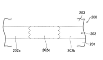
- a wiring defect portion 202c due to disconnection is generated between the normal wiring portions 202a and 202b of the wiring pattern 202 is shown.
- the microscope unit 102 observes the wiring board 200 placed on the XY table 101 to detect a wiring defect, check a correction result, and the like. Such detection or confirmation may be performed with the naked eye, or may be performed with an image captured by a camera, or automatic detection or automatic verification may be performed based on the captured image. Good.
- the pulse laser unit 103 includes, for example, a YAG laser device or the like, and forms holes 204 and 205 in the insulating film 203 of the wiring substrate 200 as will be described later to expose the normal wiring portions 202a and 202b of the wiring pattern 202. .
- the laser CVD unit 104 includes, for example, a CW laser (Continuous wave laser), supplies tungsten hexacarbonyl (W (CO) 6 ) or the like as a source gas, and is wired by light, heat, or a CVD process using light and heat. It is deposited on the substrate 200 to form a tungsten film resistant to oxidation.
- CW laser Continuous wave laser
- W (CO) 6 tungsten hexacarbonyl
- the inkjet wiring unit 105 is made to adhere to the wiring substrate 200 by ejecting a metal fine particle paste, metal ink, conductive polymer ink or the like by an inkjet method as disclosed in, for example, JP-A-2004-165588.
- it is an apparatus capable of drawing and forming a wiring pattern having a line width of 10 ⁇ m or less.
- the heater unit 106 solidifies the wiring pattern attached to the wiring board 200 by, for example, blowing heated air or irradiating laser light, by sintering or drying.
- the control unit 107 controls a sequence for sequentially operating the above units and their operations.
- the wiring defect portion 202c is detected by the microscope unit 102 while the wiring board 200 placed on the XY table 101 is scanned and moved vertically and horizontally.
- the wiring normal portions 202a and 202b on both sides of the wiring defect portion 202c are moved so as to be positioned below the pulse laser unit 103 as shown in FIG.
- the insulating film 203 covering 202 is removed by irradiation with the pulsed laser beam 211 by the pulsed laser unit 103.
- the diameter is several tens of ⁇ m, or the fineness of the wiring pattern is 10 ⁇ m or 5 ⁇ m or less, 2 to 3 ⁇ m. Are formed (zapping process).
- the holes 204 and 205 are moved so as to be positioned below the laser CVD unit 104, and a CVD laser beam 213 is irradiated while a CVD source gas 212 is supplied as schematically shown in FIG.
- electrode portions 206 and 207 contact holes made of a tungsten film are formed.
- the electrode portions 206 and 207 as described above are minute, even when more efficient CVD is performed by light and heat, deterioration of the insulating film 203 and a semiconductor element (not shown) can be easily suppressed. .
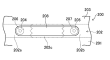
- a correction wiring pattern 208 is formed as shown in FIG. Specifically, for example, a correction wiring pattern 208 having a wiring length of 131 ⁇ m, a wiring width of 6.03 ⁇ m, an average thickness of 0.35 ⁇ m, a resistance value of 24.1 ⁇ , and a resistivity of 38.8 ⁇ ⁇ cm is formed.
- such a correction wiring pattern 208 can easily increase the film thickness and reduce the wiring resistance to, for example, 100 ⁇ / 100 ⁇ m or less, and can be connected to the normal wiring portions 202a and 202b. Since it is performed via the electrode portions 206 and 207, it is possible to easily ensure a reliable conduction state such as a contact resistance of 100 ⁇ or less. In addition, since a wide area on the wiring substrate 200 is not heated unlike a case where a wiring pattern is formed by a thermal CVD process, deterioration of the insulating film 203 and the semiconductor element can also be suppressed.
- the correction wiring pattern 208 is heated by the heater unit 106 as necessary, and is solidified by baking or drying.
- the conductive material to be deposited is a material that solidifies in a short time by evaporation of the solvent, the above-described heating is not necessarily performed.
- ultraviolet rays may be irradiated.
- the wiring defect portion 202c is not limited to the case where the wiring pattern 202 is simply interrupted as described above.
- the correction wiring pattern 208 may be formed so as to bypass the foreign substance 301 so that the wiring quality can be easily ensured.
- the electrode portions 206 and 207 are surely formed even in the minute holes 204 and 205 in which the conductive ink is difficult to adhere to the inside, and the normal wiring portion is formed.
- An increase in contact resistance with 202a and 202b can be avoided, and a wiring pattern with a significantly smaller resistance value can be formed by forming the correction wiring pattern 208 by physical adhesion of a conductive material having fluidity.
- deterioration of the insulating film 203 and the semiconductor element can be easily avoided.
- the inkjet wiring unit 105 is used to form the correction wiring pattern 208.
- the correction wiring pattern 208 is formed by adhering and solidifying a conductive material having fluidity.
- the present invention is not limited to this.
- a paste is attached to a needle having a flat tip shape to be attached to the wiring board 200, or by various printing methods.
- a wiring pattern having a remarkably small resistance value can be formed by physically attaching a conductive material having fluidity in this way.
- the XY table 101 is used to move the wiring board 200.
- the present invention is not limited to this, and the units 102 to 106 (heads) and the like are moved to the wiring board 200. It is only necessary to change the relative position of.
- correction of wiring defects as described above is not limited to the above-described series of sequences for each defect, but for each of the detected wiring defects or for all the wiring defects.
- the steps may be sequentially performed together.
- the correction of the wiring defect is not limited to the connection of the disconnection point as described above, and the wiring of defective insulation and the shorted wiring may be cut at the same time.
Landscapes
- Physics & Mathematics (AREA)
- Engineering & Computer Science (AREA)
- Nonlinear Science (AREA)
- Manufacturing & Machinery (AREA)
- Microelectronics & Electronic Packaging (AREA)
- Chemical & Material Sciences (AREA)
- Crystallography & Structural Chemistry (AREA)
- General Physics & Mathematics (AREA)
- Optics & Photonics (AREA)
- Internal Circuitry In Semiconductor Integrated Circuit Devices (AREA)
- Manufacturing Of Printed Wiring (AREA)
- Liquid Crystal (AREA)
Abstract
配線基板の欠陥を修正する配線修正装置は、配線基板200の基板上の配線パターン202上に形成された絶縁膜203に孔204を形成する絶縁膜除去装置(パルスレーザユニット103)、そこに電極部206を形成するCVD装置(レーザCVDユニット104)、配線基板200に流動性を有する導電性材料を付着固化させて修正用配線パターン208を形成する修正用配線パターン形成装置(インクジェット配線ユニット105)、これらを順次作動させる制御装置(制御部107)を有する。
Description
本発明は、例えば液晶パネルの配線基板における配線欠陥の修正等に用いられる配線基板の配線修正装置、配線基板の製造方法、配線基板、および表示装置に関するものである。
液晶パネル等の配線基板では、製造過程において導通不良となる配線欠陥が生じた場合に、修正用配線パターンを形成し、配線欠陥を修正することによって、製品の歩留まりや品質向上を図ることができる。より詳しくは、導通不良箇所の両側の配線パターンを覆う絶縁膜に孔を開けて、露出した配線パターンどうしを修正用配線パターンで接続することによって、導通不良の配線欠陥を修正することができる。
上記修正用配線パターンを形成する技術としては、レーザCVD(chemical vapor deposition)法による薄膜形成を用いる方法が知られている(例えば、特許文献1参照。)。また、インクジェット装置や先端に導電性ペーストを付着させた針を用いて導電性膜を塗布する技術も知られている(例えば、特許文献2参照。)。
しかしながら、レーザCVDを用いる場合、配線パターンとなるタングステン等の膜を厚く形成することが困難であるため、配線の抵抗値を小さくすることなどが困難であった。また、十分に製膜するためには基板の表面温度を500℃以上などにする必要がある。このため、有機材料からなる絶縁膜や半導体素子の損傷等を招きがちであるという問題点を有していた。
一方、導電性膜を導電性ペーストの塗布によって形成する場合には、その導電性ペーストを絶縁膜に開けられた孔に入り込ませて、配線パターンに確実に導通させる必要がある。ところが、絶縁膜に開けられた孔が小さいと導電性ペーストが孔の奥まで入りにくくなるため、配線パターンのピッチや配線幅が短い場合には適用が困難であるという問題点を有していた。
本発明は、上記の点に鑑み、配線欠陥修正用配線パターンの抵抗値を小さく抑えるとともに絶縁膜の損傷等を抑制することが容易にでき、しかも、配線パターンのピッチが短い場合などでも配線欠陥の修正を容易に可能にすることを目的としている。
上記の目的を達成するため、本発明は、
基板上に配線パターンと絶縁膜とが形成された配線基板の導通不良による配線欠陥を修正する配線基板の配線修正装置であって、
上記絶縁膜に孔を形成して上記配線パターンを露出させる絶縁膜除去装置と、
上記配線パターンの露出部に電極部を形成するCVD装置と、
上記配線基板における電極部、および複数の電極部を結ぶ領域に、流動性を有する導電性材料を付着、固化させて修正用配線パターンを形成する修正用配線パターン形成装置と、
上記絶縁膜除去装置、CVD装置、および修正用配線パターン形成装置を順次作動させる制御装置と、
を有することを特徴とする。
基板上に配線パターンと絶縁膜とが形成された配線基板の導通不良による配線欠陥を修正する配線基板の配線修正装置であって、
上記絶縁膜に孔を形成して上記配線パターンを露出させる絶縁膜除去装置と、
上記配線パターンの露出部に電極部を形成するCVD装置と、
上記配線基板における電極部、および複数の電極部を結ぶ領域に、流動性を有する導電性材料を付着、固化させて修正用配線パターンを形成する修正用配線パターン形成装置と、
上記絶縁膜除去装置、CVD装置、および修正用配線パターン形成装置を順次作動させる制御装置と、
を有することを特徴とする。
また、
基板上に配線パターンと絶縁膜とが形成されるとともに上記配線パターンの導通不良による配線欠陥が修正された配線基板を製造する配線基板の製造方法であって、
上記絶縁膜に孔を形成して上記配線パターンを露出させる絶縁膜除去行程と、
CVDにより上記配線パターンの露出部に電極部を形成する電極部形成行程と、
上記配線基板における電極部、および複数の電極部を結ぶ領域に、流動性を有する導電性材料を付着、固化させて修正用配線パターンを形成する修正用配線パターン形成行程と、
を有することを特徴とする。
基板上に配線パターンと絶縁膜とが形成されるとともに上記配線パターンの導通不良による配線欠陥が修正された配線基板を製造する配線基板の製造方法であって、
上記絶縁膜に孔を形成して上記配線パターンを露出させる絶縁膜除去行程と、
CVDにより上記配線パターンの露出部に電極部を形成する電極部形成行程と、
上記配線基板における電極部、および複数の電極部を結ぶ領域に、流動性を有する導電性材料を付着、固化させて修正用配線パターンを形成する修正用配線パターン形成行程と、
を有することを特徴とする。
また、
基板上に配線パターンと絶縁膜とが形成された配線基板であって、
導通不良による配線欠陥を有する配線パターンが、CVDによって形成された電極部と、
上記電極部、および複数の電極部を結ぶ領域に、流動性を有する導電性材料が付着、固化して成る修正用配線パターンによって接続されていることを特徴とする。
基板上に配線パターンと絶縁膜とが形成された配線基板であって、
導通不良による配線欠陥を有する配線パターンが、CVDによって形成された電極部と、
上記電極部、および複数の電極部を結ぶ領域に、流動性を有する導電性材料が付着、固化して成る修正用配線パターンによって接続されていることを特徴とする。
ここで、上記CVDによって形成された電極部や、流動性を有する導電性材料が付着、固化して成る修正用配線パターンは、実際上、形成される膜の厚さや性状、材料などによって明確に特定されるものであるが、これらの指標は製造方法の種々の具体的態様によって多様に変化し、かつ、それら具体的態様を包括的に表現することもできないため、当該物を構造または特性により直接特定することが不可能または非現実的なものである。
これらにより、CVDプロセスによる膜形成が行われることによって、導電性インクが内部に付着しにくいような微細な孔が絶縁膜に形成される場合でも、確実に電極部を形成して、配線パターンの配線正常部との接触抵抗の増大を回避できるとともに、流動性を有する導電性材料の物理的な付着によって修正用配線パターンを形成することによって、大幅に小さな抵抗値の配線パターンを形成することができ、しかも、絶縁膜や半導体素子の劣化等を回避することが容易にできる。
本発明によれば、配線欠陥修正用配線パターンの抵抗値を小さく抑えるとともに絶縁膜の損傷等を抑制することが容易にでき、しかも、配線パターンのピッチが短い場合などでも配線欠陥の修正が容易に可能になる。
以下、本発明の実施形態を図面に基づいて詳細に説明する。
(配線修正装置100の構成)
本実施形態の配線修正装置100は、図1に示すように、XYテーブル101、顕微鏡ユニット102、パルスレーザユニット103(絶縁膜除去装置)、レーザCVDユニット104(CVD装置)、インクジェット配線ユニット105(修正用配線パターン形成装置)、ヒータユニット106、および制御部107(制御装置)を備えて構成されている。
本実施形態の配線修正装置100は、図1に示すように、XYテーブル101、顕微鏡ユニット102、パルスレーザユニット103(絶縁膜除去装置)、レーザCVDユニット104(CVD装置)、インクジェット配線ユニット105(修正用配線パターン形成装置)、ヒータユニット106、および制御部107(制御装置)を備えて構成されている。
上記XYテーブル101は、例えば図2、図3に模式的に示すような液晶表示パネルや有機EL(electroluminescent)表示パネル等を構成する配線基板200が載置されて、その処理対象部分を各ユニットの下方に移動させるものである。上記配線基板200は、例えば、ガラス基板201上にアルミニウムや銅から成るゲート線やソース線などの配線パターン202、および絶縁膜203が積層されて形成されたもので、同図に示す例では、配線パターン202の配線正常部202a・202bの間に断線による配線欠陥部202cが生じている状態を示している。
上記顕微鏡ユニット102は、XYテーブル101上に載置された配線基板200を観察して配線欠陥の検出や修正結果の確認等を行うものである。なお、このような検出や確認等は肉眼で行われたり、カメラで撮像した画像で行われたりしてもよく、また、撮像した画像に基づいて自動検出や自動検証が行われるなどしてもよい。
パルスレーザユニット103は、例えばYAGレーザ装置等を備え、配線基板200の絶縁膜203に後述するように孔204・205を形成して配線パターン202の配線正常部202a・202bを露出させるものである。
レーザCVDユニット104は、例えば、CWレーザ(Continuous wave laser)を備え、タングステンヘキサカルボニル(W(CO)6) 等を原料ガスとして供給して、光、熱、または光および熱によるCVDプロセスにより配線基板200上に堆積させ、酸化に強いタングステン膜を形成するものである。
インクジェット配線ユニット105は、例えば特開2004-165587号公報に示されるようなインクジェット方式により、金属微粒子のペーストや、金属インク、導電性高分子のインク等を吐出して配線基板200に付着させ、例えば10μm以下の線幅の配線パターンを描画して形成し得る装置である。
ヒータユニット106は、例えば加熱空気の吹きつけやレーザ光の照射などによって配線基板200に付着させた配線パターンを焼成(sintering)や乾燥によって固化させるものである。
制御部107は、上記各部を順次作動させるシーケンスや、それらの動作を制御するものである。
(配線修正装置100の動作)
次に、上記のように構成された配線修正装置100による配線基板200の配線パターンの修正について説明する。
次に、上記のように構成された配線修正装置100による配線基板200の配線パターンの修正について説明する。
(1)まず、XYテーブル101に載置された配線基板200が縦横に走査移動させられながら、顕微鏡ユニット102によって配線欠陥部202cが検出される。
(2)配線欠陥部202cが検出されると、図4に示すように配線欠陥部202cの両側の配線正常部202a・202bがパルスレーザユニット103の下方に位置するように移動させられ、配線パターン202を覆っている絶縁膜203がパルスレーザユニット103によるパルスレーザビーム211の照射によって除去されることにより、例えば直径が数十μmや、配線パターンの微細程度によっては10μmや5μm以下、2~3μmなどの微細な孔204・205が形成される(zappingプロセス)。
(3)次に、上記孔204・205がレーザCVDユニット104の下方に位置するように移動させられ、図5に模式的に示すようにCVD原料ガス212が供給されながらCVDレーザビーム213が照射されることによって、タングステン膜による電極部206・207(コンタクトホール)が形成される。ここで、上記のようなCVDプロセスによる膜形成が行われることによって、導電性インクが内部に付着しにくいような微細な孔204・205でも、確実に電極部206・207を形成することが容易にできる。また、上記のような電極部206・207は微小なので、光および熱によって、より効率のよいCVDが行われる場合でも、絶縁膜203や図示しない半導体素子の劣化などを抑制することが容易にできる。
(4)その後、配線欠陥部202cを挟む配線正常部202a・202bに亘る領域が、インクジェット配線ユニット105の下方を通過するように移動させられながら、流動性を有する導電性材料が配線基板200に付着して描画されることにより、図6に示すように修正用配線パターン208が形成される。具体的には、例えば配線長が131μm、配線幅が6.03μm、平均厚さが0.35μm、抵抗値が24.1Ω、抵抗率が38.8μΩ・cmの修正用配線パターン208が形成される。このような修正用配線パターン208は、CVDプロセスに比べて、膜厚を厚くして配線抵抗を例えば100Ω/100μm以下にすることなどが容易にできるとともに、配線正常部202a・202bとの接続が電極部206・207を介して行われるので、例えば接触抵抗が100Ω以下などの確実な導通状態を確保することが容易にできる。また、熱CVDプロセスによって配線パターンが形成される場合のように配線基板200上の広範な領域が加熱されることもないので、やはり絶縁膜203や半導体素子の劣化などを抑制することができる。
(5)上記修正用配線パターン208は、必要に応じてヒータユニット106により加熱され、焼成や乾燥によって固化する。なお、付着させる導電性材料として、溶剤の蒸発により短時間に固化するものが用いられる場合には必ずしも上記のような加熱をしなくてもよい。また、例えば紫外線によって固化するような材料が用いられる場合には、紫外線を照射するようにしたりしてもよい。
(変形例)
配線欠陥部202cは、上記のように単に配線パターン202が途切れたものに限らず、例えば図8に示すように異物301の付着によって配線欠陥部202cが生じたような場合には、同図に示すように異物301を迂回するように修正用配線パターン208を形成するなどして、配線品質を容易に確保できるようにしてもよい。
配線欠陥部202cは、上記のように単に配線パターン202が途切れたものに限らず、例えば図8に示すように異物301の付着によって配線欠陥部202cが生じたような場合には、同図に示すように異物301を迂回するように修正用配線パターン208を形成するなどして、配線品質を容易に確保できるようにしてもよい。
上記のように、CVDプロセスによる膜形成が行われることによって、導電性インクが内部に付着しにくいような微細な孔204・205でも、確実に電極部206・207を形成して、配線正常部202a・202bとの接触抵抗の増大を回避できるとともに、流動性を有する導電性材料の物理的な付着によって修正用配線パターン208を形成することによって、大幅に小さな抵抗値の配線パターンを形成することができ、しかも、絶縁膜203や半導体素子の劣化等を回避することが容易にできる。
(その他の事項)
なお、上記の例では修正用配線パターン208を形成するためにインクジェット配線ユニット105が用いられる例を示したが、流動性を有する導電性材料を付着、固化させることによる修正用配線パターン208の形成は、これに限らず、例えば特開平8-292442号公報に開示されているように先端形状を平坦にした針にペーストを付着させて配線基板200に付着させるようにしたり、種々の印刷手法によって付着させるようにしたりしてもよく、このように流動性を有する導電性材料を物理的に付着することによって、大幅に小さな抵抗値の配線パターンを形成することができる。
なお、上記の例では修正用配線パターン208を形成するためにインクジェット配線ユニット105が用いられる例を示したが、流動性を有する導電性材料を付着、固化させることによる修正用配線パターン208の形成は、これに限らず、例えば特開平8-292442号公報に開示されているように先端形状を平坦にした針にペーストを付着させて配線基板200に付着させるようにしたり、種々の印刷手法によって付着させるようにしたりしてもよく、このように流動性を有する導電性材料を物理的に付着することによって、大幅に小さな抵抗値の配線パターンを形成することができる。
また、上記の例ではXYテーブル101を用いて配線基板200を移動させる例を示したが、これに限らず、各ユニット102~106(ヘッド)等を移動させるなどして、これらと配線基板200との相対位置が変えられるようにされればよい。
また、上記のような配線欠陥の修正は、各欠陥ごとに上記のような一連のシーケンスを行うのに限らず、検出された複数の配線欠陥ごとに、または全ての配線欠陥に対して、各工程が順次まとめて行われるようにしてもよい。
また、配線欠陥の修正は、上記のように断線箇所の接続だけが行われるのに限らず、絶縁不良の配線やショートした配線の切断も併せて行われるようにしてもよい。
100 配線修正装置
101 XYテーブル
102 顕微鏡ユニット
103 パルスレーザユニット
104 レーザCVDユニット
105 インクジェット配線ユニット
106 ヒータユニット
107 制御部
200 配線基板
201 ガラス基板
202 配線パターン
202a・202b 配線正常部
202c 配線欠陥部
203 絶縁膜
204・205 孔
206・207 電極部
208 修正用配線パターン
211 パルスレーザビーム
212 CVD原料ガス
213 CVDレーザビーム
301 異物
101 XYテーブル
102 顕微鏡ユニット
103 パルスレーザユニット
104 レーザCVDユニット
105 インクジェット配線ユニット
106 ヒータユニット
107 制御部
200 配線基板
201 ガラス基板
202 配線パターン
202a・202b 配線正常部
202c 配線欠陥部
203 絶縁膜
204・205 孔
206・207 電極部
208 修正用配線パターン
211 パルスレーザビーム
212 CVD原料ガス
213 CVDレーザビーム
301 異物
Claims (8)
- 基板上に配線パターンと絶縁膜とが形成された配線基板の導通不良による配線欠陥を修正する配線基板の配線修正装置であって、
上記絶縁膜に孔を形成して上記配線パターンを露出させる絶縁膜除去装置と、
上記配線パターンの露出部に電極部を形成するCVD装置と、
上記配線基板における電極部、および複数の電極部を結ぶ領域に、流動性を有する導電性材料を付着、固化させて修正用配線パターンを形成する修正用配線パターン形成装置と、
上記絶縁膜除去装置、CVD装置、および修正用配線パターン形成装置を順次作動させる制御装置と、
を有することを特徴とする配線修正装置。 - 請求項1の配線修正装置であって、
上記絶縁膜除去装置は、パルスレーザによって上記絶縁膜に孔を形成するように構成され、
上記CVD装置は、原料ガスの供給、およびレーザ光の照射によって上記電極部を形成するように構成されていることを特徴とする配線修正装置。 - 請求項1または請求項2の配線修正装置であって、
上記絶縁膜除去装置は、上記絶縁膜に直径が10μm以下の上記孔を形成するように構成されていることを特徴とする配線修正装置。 - 請求項1から請求項3のうち何れか1項の配線修正装置であって、
上記修正用配線パターン形成装置は、上記流動性を有する導電性材料をインクジェットまたは塗布により上記配線基板に付着させるように構成されていることを特徴とする配線修正装置。 - 基板上に配線パターンと絶縁膜とが形成されるとともに上記配線パターンの導通不良による配線欠陥が修正された配線基板を製造する配線基板の製造方法であって、
上記絶縁膜に孔を形成して上記配線パターンを露出させる絶縁膜除去行程と、
CVDにより上記配線パターンの露出部に電極部を形成する電極部形成行程と、
上記配線基板における電極部、および複数の電極部を結ぶ領域に、流動性を有する導電性材料を付着、固化させて修正用配線パターンを形成する修正用配線パターン形成行程と、
を有することを特徴とする配線基板の製造方法。 - 基板上に配線パターンと絶縁膜とが形成された配線基板であって、
導通不良による配線欠陥を有する配線パターンが、CVDによって形成された電極部と、
上記電極部、および複数の電極部を結ぶ領域に、流動性を有する導電性材料が付着、固化して成る修正用配線パターンによって接続されていることを特徴とする配線基板。 - 請求項6の配線基板が用いられた表示パネルを有することを特徴とする表示装置。
- 請求項7の表示装置であって、
上記表示パネルが、液晶表示パネル、または有機EL表示パネルであることを特徴とする表示装置。
Applications Claiming Priority (2)
| Application Number | Priority Date | Filing Date | Title |
|---|---|---|---|
| JP2016-015675 | 2016-01-29 | ||
| JP2016015675A JP2017135318A (ja) | 2016-01-29 | 2016-01-29 | 配線基板の配線修正装置、配線基板の製造方法、配線基板、および表示装置 |
Publications (1)
| Publication Number | Publication Date |
|---|---|
| WO2017130530A1 true WO2017130530A1 (ja) | 2017-08-03 |
Family
ID=59397759
Family Applications (1)
| Application Number | Title | Priority Date | Filing Date |
|---|---|---|---|
| PCT/JP2016/084126 Ceased WO2017130530A1 (ja) | 2016-01-29 | 2016-11-17 | 配線基板の配線修正装置、配線基板の製造方法、配線基板、および表示装置 |
Country Status (3)
| Country | Link |
|---|---|
| JP (1) | JP2017135318A (ja) |
| TW (1) | TWI707614B (ja) |
| WO (1) | WO2017130530A1 (ja) |
Families Citing this family (2)
| Publication number | Priority date | Publication date | Assignee | Title |
|---|---|---|---|---|
| CN109613773B (zh) * | 2019-01-08 | 2021-12-07 | 京东方科技集团股份有限公司 | 一种基板中不良导线的修复方法 |
| CN111446173A (zh) * | 2020-03-16 | 2020-07-24 | 林杰 | 一种布线断线修复工艺 |
Citations (7)
| Publication number | Priority date | Publication date | Assignee | Title |
|---|---|---|---|---|
| JPH09237768A (ja) * | 1995-12-28 | 1997-09-09 | Nippon Steel Corp | 半導体装置及びその製造方法 |
| JPH11145142A (ja) * | 1997-11-07 | 1999-05-28 | Toshiba Corp | 半導体装置及びその製造方法 |
| JP2002359446A (ja) * | 2001-05-31 | 2002-12-13 | Hitachi Ltd | 配線基板およびその製造方法 |
| JP2006171610A (ja) * | 2004-12-20 | 2006-06-29 | Toshiba Matsushita Display Technology Co Ltd | 液晶表示装置及びその製造方法 |
| JP2007059890A (ja) * | 2005-07-29 | 2007-03-08 | Semiconductor Energy Lab Co Ltd | 半導体装置およびその作製方法 |
| JP2010514926A (ja) * | 2006-12-26 | 2010-05-06 | コーウィン ディーエスティー カンパニー リミテッド | レーザーを用いた金属薄膜形成装置およびその方法 |
| JP2012199404A (ja) * | 2011-03-22 | 2012-10-18 | Ntn Corp | パターン修正方法 |
Family Cites Families (1)
| Publication number | Priority date | Publication date | Assignee | Title |
|---|---|---|---|---|
| TW201034080A (en) * | 2009-03-10 | 2010-09-16 | Chi Mei Optoelectronics Corp | Substrate and method for repairing matrix wire thereof |
-
2016
- 2016-01-29 JP JP2016015675A patent/JP2017135318A/ja active Pending
- 2016-11-17 WO PCT/JP2016/084126 patent/WO2017130530A1/ja not_active Ceased
- 2016-12-07 TW TW105140425A patent/TWI707614B/zh not_active IP Right Cessation
Patent Citations (7)
| Publication number | Priority date | Publication date | Assignee | Title |
|---|---|---|---|---|
| JPH09237768A (ja) * | 1995-12-28 | 1997-09-09 | Nippon Steel Corp | 半導体装置及びその製造方法 |
| JPH11145142A (ja) * | 1997-11-07 | 1999-05-28 | Toshiba Corp | 半導体装置及びその製造方法 |
| JP2002359446A (ja) * | 2001-05-31 | 2002-12-13 | Hitachi Ltd | 配線基板およびその製造方法 |
| JP2006171610A (ja) * | 2004-12-20 | 2006-06-29 | Toshiba Matsushita Display Technology Co Ltd | 液晶表示装置及びその製造方法 |
| JP2007059890A (ja) * | 2005-07-29 | 2007-03-08 | Semiconductor Energy Lab Co Ltd | 半導体装置およびその作製方法 |
| JP2010514926A (ja) * | 2006-12-26 | 2010-05-06 | コーウィン ディーエスティー カンパニー リミテッド | レーザーを用いた金属薄膜形成装置およびその方法 |
| JP2012199404A (ja) * | 2011-03-22 | 2012-10-18 | Ntn Corp | パターン修正方法 |
Also Published As
| Publication number | Publication date |
|---|---|
| TWI707614B (zh) | 2020-10-11 |
| JP2017135318A (ja) | 2017-08-03 |
| TW201728243A (zh) | 2017-08-01 |
Similar Documents
| Publication | Publication Date | Title |
|---|---|---|
| US9111886B2 (en) | Method of repairing a defect of an organic EL display | |
| WO2015155662A1 (en) | Pulsed-mode direct-write laser metallization | |
| JP2007504661A (ja) | インクジェット技術を利用した細線形成方法およびシステム | |
| JP2017135318A (ja) | 配線基板の配線修正装置、配線基板の製造方法、配線基板、および表示装置 | |
| WO2011118092A1 (ja) | プリント配線板の製造方法 | |
| WO2013129165A1 (ja) | ガラス基板を製造する方法、およびガラス基板 | |
| JP5254627B2 (ja) | 電子回路のパターン欠損修復方法およびその装置 | |
| TW201725768A (zh) | 有機el顯示裝置之製造方法 | |
| WO2008078944A1 (en) | Apparatus and method for forming thin metal film using laser | |
| JP2016072362A (ja) | 金属配線基板の欠陥修正方法、電子素子の製造方法、および金属配線基板の欠陥修正装置 | |
| JP2011071376A (ja) | 回路基板の欠陥修正方法、回路基板及び半導体装置 | |
| US20210168942A1 (en) | Conductive pattern, method for forming conductive pattern, and disconnection repairing method | |
| CN103548174B (zh) | 用于制造图案化层的制造设备和方法以及电学器件 | |
| JP3649221B2 (ja) | Tft基板の配線修正方法 | |
| CN120435683A (zh) | 用于接触pdlc坯件的方法 | |
| JPH088514A (ja) | 電子回路基板上への液体材料の局所供給方法及びその装置 | |
| Feng et al. | Laser patterning of printed silver for selective lighting of electroluminescence film | |
| KR102781067B1 (ko) | 비아 홀 전극의 형성 방법, 비아 홀 전극의 리페어 방법, 및 인쇄회로기판 | |
| KR102454738B1 (ko) | 잉크젯 방식으로 배선을 제조하는 방법 및 장치 | |
| KR102060222B1 (ko) | 미세 배선 형성 방법 | |
| KR20210120301A (ko) | 미세 전극의 리페어 방법 | |
| JP2009103965A (ja) | 欠陥修正方法 | |
| JP5339342B2 (ja) | 表示装置の修正方法およびその装置 | |
| JP2012199404A (ja) | パターン修正方法 | |
| JP6996007B2 (ja) | 回路製造システム |
Legal Events
| Date | Code | Title | Description |
|---|---|---|---|
| 121 | Ep: the epo has been informed by wipo that ep was designated in this application |
Ref document number: 16888115 Country of ref document: EP Kind code of ref document: A1 |
|
| NENP | Non-entry into the national phase |
Ref country code: DE |
|
| 122 | Ep: pct application non-entry in european phase |
Ref document number: 16888115 Country of ref document: EP Kind code of ref document: A1 |