WO2017126185A1 - 水晶振動子及びその製造方法 - Google Patents
水晶振動子及びその製造方法 Download PDFInfo
- Publication number
- WO2017126185A1 WO2017126185A1 PCT/JP2016/082531 JP2016082531W WO2017126185A1 WO 2017126185 A1 WO2017126185 A1 WO 2017126185A1 JP 2016082531 W JP2016082531 W JP 2016082531W WO 2017126185 A1 WO2017126185 A1 WO 2017126185A1
- Authority
- WO
- WIPO (PCT)
- Prior art keywords
- crystal resonator
- crystal
- frame body
- package member
- recess
- Prior art date
- Legal status (The legal status is an assumption and is not a legal conclusion. Google has not performed a legal analysis and makes no representation as to the accuracy of the status listed.)
- Ceased
Links
Images








Classifications
-
- H—ELECTRICITY
- H03—ELECTRONIC CIRCUITRY
- H03H—IMPEDANCE NETWORKS, e.g. RESONANT CIRCUITS; RESONATORS
- H03H9/00—Networks comprising electromechanical or electro-acoustic elements; Electromechanical resonators
- H03H9/15—Constructional features of resonators consisting of piezoelectric or electrostrictive material
- H03H9/17—Constructional features of resonators consisting of piezoelectric or electrostrictive material having a single resonator
- H03H9/19—Constructional features of resonators consisting of piezoelectric or electrostrictive material having a single resonator consisting of quartz
-
- H—ELECTRICITY
- H03—ELECTRONIC CIRCUITRY
- H03H—IMPEDANCE NETWORKS, e.g. RESONANT CIRCUITS; RESONATORS
- H03H3/00—Apparatus or processes specially adapted for the manufacture of impedance networks, resonating circuits, resonators
- H03H3/007—Apparatus or processes specially adapted for the manufacture of impedance networks, resonating circuits, resonators for the manufacture of electromechanical resonators or networks
- H03H3/02—Apparatus or processes specially adapted for the manufacture of impedance networks, resonating circuits, resonators for the manufacture of electromechanical resonators or networks for the manufacture of piezoelectric or electrostrictive resonators or networks
-
- H—ELECTRICITY
- H03—ELECTRONIC CIRCUITRY
- H03H—IMPEDANCE NETWORKS, e.g. RESONANT CIRCUITS; RESONATORS
- H03H9/00—Networks comprising electromechanical or electro-acoustic elements; Electromechanical resonators
- H03H9/02—Details
- H03H9/05—Holders or supports
- H03H9/0595—Holders or supports the holder support and resonator being formed in one body
-
- H—ELECTRICITY
- H03—ELECTRONIC CIRCUITRY
- H03H—IMPEDANCE NETWORKS, e.g. RESONANT CIRCUITS; RESONATORS
- H03H9/00—Networks comprising electromechanical or electro-acoustic elements; Electromechanical resonators
- H03H9/02—Details
- H03H9/05—Holders or supports
- H03H9/10—Mounting in enclosures
- H03H9/1007—Mounting in enclosures for bulk acoustic wave [BAW] devices
- H03H9/1035—Mounting in enclosures for bulk acoustic wave [BAW] devices the enclosure being defined by two sealing substrates sandwiching the piezoelectric layer of the BAW device
-
- H—ELECTRICITY
- H03—ELECTRONIC CIRCUITRY
- H03H—IMPEDANCE NETWORKS, e.g. RESONANT CIRCUITS; RESONATORS
- H03H9/00—Networks comprising electromechanical or electro-acoustic elements; Electromechanical resonators
- H03H9/02—Details
- H03H9/125—Driving means, e.g. electrodes, coils
- H03H9/13—Driving means, e.g. electrodes, coils for networks consisting of piezoelectric or electrostrictive materials
-
- H—ELECTRICITY
- H03—ELECTRONIC CIRCUITRY
- H03H—IMPEDANCE NETWORKS, e.g. RESONANT CIRCUITS; RESONATORS
- H03H3/00—Apparatus or processes specially adapted for the manufacture of impedance networks, resonating circuits, resonators
- H03H3/007—Apparatus or processes specially adapted for the manufacture of impedance networks, resonating circuits, resonators for the manufacture of electromechanical resonators or networks
- H03H3/02—Apparatus or processes specially adapted for the manufacture of impedance networks, resonating circuits, resonators for the manufacture of electromechanical resonators or networks for the manufacture of piezoelectric or electrostrictive resonators or networks
- H03H2003/022—Apparatus or processes specially adapted for the manufacture of impedance networks, resonating circuits, resonators for the manufacture of electromechanical resonators or networks for the manufacture of piezoelectric or electrostrictive resonators or networks the resonators or networks being of the cantilever type
Definitions
- the present invention relates to a crystal resonator and a manufacturing method thereof.
- a crystal resonator used for an oscillation device or a bandpass filter a crystal resonator having a thickness-shear vibration as a main vibration is widely used.
- a structure having a crystal diaphragm and a pair of sealing members respectively disposed on the upper and lower surfaces of the crystal diaphragm via a bonding material is known (Patent Document 1). reference).
- the bonding material is formed of a metal brazing material or the like, and the vibration portion of the crystal vibration plate is hermetically sealed by bonding the crystal vibration plate to each sealing member through the bonding material.
- Patent Document 1 when the quartz crystal diaphragm and each sealing member are joined by a joining material, a space corresponding to the thickness of the joining material is generated inside the crystal unit, and the wafer is separated into individual pieces. In some cases, wafer cracking is likely to occur during the cutting process.
- the quartz diaphragm and each sealing member are directly joined, the joining strength between the quartz diaphragm and each sealing member may be reduced due to the influence of the protrusion of the extraction electrode formed in the joining region.
- the present invention has been made in view of such circumstances, and it is intended to improve the bonding strength between the frame body of the crystal resonator element and the package member for housing the crystal piece, and to improve the reliability of the product. Objective.
- a crystal resonator includes a crystal piece in which a pair of excitation electrodes facing each other is formed, a frame body that surrounds the outer periphery of the crystal piece, and a connecting member that connects the frame body and the crystal piece.
- a crystal vibration element including: a package member joined to the entire circumference of the frame body on at least one side of the pair of excitation electrodes; and an extraction electrode electrically connected to one of the pair of excitation electrodes, At least one of the frame body and the package member is formed with a recess in a joint region where the frame body and the package member are joined, and the extraction electrode has a thickness not exceeding the depth of the recess in the joint region. Provided in the recess.
- the present invention it is possible to improve the bonding strength between the frame of the crystal resonator element and the package member for housing the crystal piece, and to improve the reliability of the product.
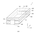
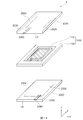
- FIG. 1 is an exploded perspective view of the crystal resonator according to the first embodiment of the present invention.
- FIG. 2 is a perspective view of the crystal resonator according to the first embodiment of the present invention.
- FIG. 3 is a plan view of the crystal resonator element according to the first embodiment of the invention.
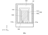
- FIG. 4 is a plan view of the crystal resonator element according to the first embodiment of the invention.
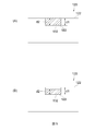
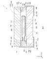
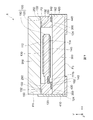
- 5A and 5B are cross-sectional views taken along line VV in FIG. 6 is a cross-sectional view taken along line VI-VI in FIG. 7 is a cross-sectional view taken along line VII-VII in FIG.
- FIG. 8 is a flowchart showing a method for manufacturing a crystal resonator according to the first embodiment of the present invention.
- FIGS. 1 is an exploded perspective view of the crystal resonator according to the first embodiment of the present invention.
- FIG. 2 is a perspective view of the crystal resonator according to the first embodiment of the present invention
- FIG. 9A to 9C are views for explaining a method of manufacturing a crystal resonator according to the first embodiment of the present invention.
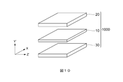
- FIG. 10 is a perspective view of the substrate for explaining the manufacturing method of the crystal unit according to the first embodiment of the present invention.
- FIG. 11 is a perspective view of a laminated member for explaining the method for manufacturing a crystal resonator according to the first embodiment of the present invention.
- FIG. 12 is an exploded perspective view of a crystal resonator according to a modification of the first embodiment of the present invention.
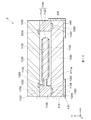
- 13 is a cross-sectional view taken along line XIII-XIII in FIG.
- FIG. 14 is an exploded perspective view of the crystal resonator according to the second embodiment of the invention.
- FIG. 10 is a perspective view of the substrate for explaining the manufacturing method of the crystal unit according to the first embodiment of the present invention.
- FIG. 11 is a perspective view of a laminated member for explaining the method for manufacturing a crystal resonator according to the first embodiment of
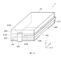
- FIG. 15 is a perspective view of a crystal resonator according to the second embodiment of the present invention.
- FIG. 16 is an exploded perspective view of a crystal resonator according to a modification of the second embodiment of the present invention.
- FIG. 17 is an exploded perspective view of a crystal resonator according to another modification of the second embodiment of the present invention.
- FIG. 1 is an exploded perspective view of the crystal resonator according to the present embodiment
- FIG. 2 is a perspective view of the crystal resonator
- FIGS. 3 and 4 are plan views of the crystal resonator element.
- 5A and 5B are cross-sectional views taken along line VV in FIG. 3
- FIG. 6 is a cross-sectional view taken along line VI-VI in FIG. 1
- FIG. 7 is a cross-sectional view taken along line VII-VII in FIG. .
- the crystal resonator 1 includes a crystal resonator element 100 (Quartz Crystal Resonator), a lid member 200, a base member 300, and external electrodes 410, 420, and 430. , 440.
- the external electrodes 410, 420, 430, and 440 are omitted, and the same applies to the following exploded perspective views (FIGS. 12, 14, 16, and 17).
- the crystal resonator element 100 is formed of, for example, an AT cut crystal substrate.
- the AT-cut quartz substrate has an X-axis, a Y-axis, and a Z-axis which are crystal axes of the artificial quartz, and the Y-axis and the Z-axis are 35 degrees 15 minutes ⁇ 1 in the direction from the Y-axis to the Z-axis
- the axes rotated for 30 minutes are defined as the Y ′ axis and the Z ′ axis, respectively, the surfaces parallel to the plane specified by the X axis and the Z ′ axis are cut out.
- a quartz resonator element using an AT-cut quartz substrate has extremely high frequency stability over a wide temperature range, is excellent in aging characteristics, and can be manufactured at low cost.
- the AT-cut crystal resonator element often uses a thickness shear vibration mode as a main vibration.
- each configuration of the crystal resonator will be described with reference to the axial direction of the AT cut.
- the lid member 200 and the base member 300 are both examples of package members, and are joined to the crystal resonator element 100 so as to accommodate a part of the crystal resonator element 100 (at least a crystal piece).
- the crystal resonator element 100, the lid member 200, and the base member 300 have substantially the same planar shape (for example, a rectangular shape) in plan view as viewed from the thickness direction of each member.
- the crystal resonator element 100 includes a crystal piece 110 (Quartz Crystal Blank), a frame body 120 that surrounds the outer periphery of the crystal piece 110, and connecting members 111 a and 111 b that connect the crystal piece 110 and the frame body 120.
- the crystal piece 110, the frame body 120, and the connecting members 111a and 111b are all formed from, for example, an AT-cut crystal substrate.
- the quartz resonator element 100 as a whole has a long side parallel to the X axis, a short side parallel to the Z ′ axis, and a thickness parallel to the Y ′ axis.
- the crystal piece 110 is provided apart from the frame body 120, and both are connected by at least one connecting member (two connecting members 111a and 111b in the example shown in FIG. 1). As shown in FIG. 1, the connecting members 111 a and 111 b are disposed at one end (X-axis negative direction side) of the crystal piece 110 in the X-axis direction.
- the number of connecting members and the arrangement thereof are not particularly limited. For example, one connecting member may be provided at one end of the crystal piece 110 in the X-axis direction, or two connecting members may be provided. One of the members may be provided at one end of the crystal piece 110 in the X-axis direction, and the other may be provided at the other end in the X-axis direction.
- the thickness of the crystal resonator element 100 parallel to the Y ′ axis is not particularly limited, but for example, the thickness gradually decreases in the order of the frame body 120, the crystal piece 110, and the connecting members 111a and 111b ( 6 and 7).
- a space in which the crystal piece 110 can vibrate can be easily obtained when a package member (for example, the lid member 200 or the base member 300) is joined to the crystal piece 110. Can be secured.
- the frame member and the crystal piece have the same thickness, and the lid member and the base member are bonded to the surface of the crystal vibration element on the side where Y ′ is formed so as to form an internal space in which the crystal piece is accommodated.
- An axial recess may be provided.
- FIG. 3 is a plan view seen from the first surface 112 of the crystal piece 110 according to the present embodiment and the first surface 122 side of the frame body 120
- FIG. 4 is a second view of the crystal piece 110 according to the present embodiment
- FIG. 6 is a plan view of the surface 114 and the frame body 120 as viewed from the second surface 124 side.
- the first excitation electrode 130 and the second excitation electrode 140 are formed on the pair of main surfaces of the crystal piece 110.
- the first excitation electrode 130 is formed on the first surface 112 (the surface on the Y′-axis positive direction side) of the crystal piece 110
- the second excitation electrode 140 is the second surface of the crystal piece 110.
- 114 surface on the Y′-axis negative direction side.
- the 1st excitation electrode 130 and the 2nd excitation electrode 140 are arrange
- an extraction electrode 132 that is electrically connected to the first excitation electrode 130 is formed on the first surface 122 of the frame body 120.
- an extraction electrode 142 that is electrically connected to the second excitation electrode 140 is formed on the second surface 124 of the frame body 120.
- the extraction electrode 132 is extracted from the first excitation electrode 130 through the one coupling member 111 a onto the first surface 122 of the frame body 120, and on the X axis negative direction side on the surface. It is pulled out so as to be in contact with one side L1.
- the extraction electrode 142 is extracted from the second excitation electrode 140 through the other coupling member 111 b onto the second surface 124 of the frame body 120, and the X-axis positive direction on the surface It is pulled out so as to be in contact with one side L2 (side opposite to L1).
- an external electrode (described later) that is electrically connected to one of the extraction electrodes 132 and 142 can be provided on each of opposite sides in the X-axis direction.
- the direction in which the extraction electrodes 132 and 142 are extracted is not limited to the X-axis direction, and may be, for example, the Z′-axis direction, and can be appropriately changed according to the formation position of the external electrode.
- the extraction electrode 132 is extracted so as to surround the entire circumference of the first surface 122 of the frame body 120 (see FIG. 3), while the extraction electrode 142 is the entire circumference of the second surface 124 of the frame body 120. (See FIG. 4), and in a plan view viewed from the Y′-axis direction, the respective extraction electrodes 132 and 142 are provided so that at least a part thereof does not overlap with each other. More specifically, in the illustrated example, the extraction electrode 132 is provided near the inner periphery of the frame body 120 except for at least one side (for example, one side L1), while the extraction electrode 142 is provided near the outer periphery of the frame body 120. It is done. Thereby, since the distance between both extraction electrodes 132 and 142 can be ensured long, the influence of the noise which one extraction electrode exerts on the other extraction electrode can be reduced.
- the extraction electrodes 132 and 142 are formed so as to surround the entire circumference on the first surface 122 and the second surface 124 of the frame body 120, but the arrangement of these extraction electrodes is particularly limited. It is not something. That is, the extraction electrodes 132 and 142 need only be extracted until they are in contact with one of the end surfaces of the frame 120, and do not need to surround the entire circumference of the frame 120.
- An inspection electrode 134 is formed on the first surface 122 of the frame 120.
- the inspection electrode 134 is electrically connected to an extraction electrode 142 (electrically connected to the second excitation electrode 140) formed on the second surface 124 side facing the first surface 122.
- electrical inspection of the first and second excitation electrodes 130 and 140 can be performed from one side of the frame body 120 (for example, the first surface 122 side). Therefore, an electrical test for confirming the operation of the crystal resonator element 100 can be easily performed.
- the extraction electrodes 132 and 142 and the inspection electrode 134 are provided in the recesses formed in the first surface 122 and the second surface 124 of the frame body 120. The same applies to a perspective view and a plan view described later.
- the electrodes including the first and second excitation electrodes 130 and 140 and the extraction electrodes 132 and 142 include, for example, a base made of a chromium (Cr) layer and a gold (Au) layer formed on the surface of the chromium layer.
- the material is not limited.
- the lid member 200 is disposed on the first surface 122 side (one side) of the frame body 120, and the base member 300 is disposed on the second surface 124 side (side of the frame body 120).
- the lid member 200, the crystal resonator element 100, and the base member 300 are arranged on the other side, and have a three-layer structure in the order of the lamination.
- the thicknesses of the lid member 200, the crystal resonator element 100, and the base member 300 are not particularly limited.
- the lid member 200 and the base member 300 are slightly more than the frame body 120 of the crystal resonator element 100. It may be thick.
- the lid member 200 is bonded to the entire circumference of the first surface 122 of the frame body 120 of the crystal resonator element 100, and the base member 300 is bonded to the entire periphery of the second surface 124 of the frame body 120 of the crystal resonator element 100. Yes.
- the crystal piece 110 is hermetically sealed in the internal space (cavity).
- the bonding region 250 of the lid member 200 (the region where the frame body 120 is bonded in the surface on the Y′-axis negative direction side of the lid member 200) and the first surface 122 (bonding region) of the frame body 120 are adhesives.
- a bonding member 350 for bonding both of them such as a glass bonding material, and a bonding region 350 of the base member 300 (the frame body 120 is bonded to the surface of the base member 300 on the Y′-axis positive direction side). Area) and the second surface 124 (bonding area) of the frame 120 are also directly bonded in the same manner. This eliminates the need for a bonding member and can suppress, for example, bonding peeling due to stress concentration caused by a difference in thermal expansion or elastic modulus of the bonding member with respect to the crystal resonator element 100, the lid member 200, and the base member 300. .
- the lid member 200 and the frame body 120 and the base member 300 and the frame body 120 may be joined via the joining member.
- the material of the bonding member is not limited as long as the bonding regions can be bonded together and the internal space can be hermetically sealed.
- glass bonding such as low melting point glass (for example, lead borate or tin phosphate) is possible. It may be a material, or a resin adhesive (for example, an epoxy adhesive) may be used.
- the material of the lid member 200 and the base member 300 is not particularly limited, for example, the lid member 200 and the base member 300 are preferably made of the same material as the crystal resonator element 100, and may be made of, for example, crystal. According to this, since each member to be joined is made of the same material, the thermal expansion coefficient is approximated, and the residual stress at the time of joining can be reduced. In particular, when the lid member 200 and the base member 300 are made of the same AT-cut quartz crystal as that of the quartz resonator element 100, in addition to the same material, the crystal axis direction is also the same, so the thermal expansion coefficient is The residual stress at the time of joining can be further reduced.
- the lid member 200 and the base member 300 may be made of a material other than quartz, for example, a glass material, a quartz material, or a glass epoxy resin in which a glass fiber is impregnated with an epoxy resin.
- the lid member 200 and the base member 300 are, for example, flat members as shown in FIG. Further, the first surface 122 and the second surface 124 of the frame body 120, the joining region 250 of the lid member 200, and the joining region 350 of the base member 300 may have a root mean square roughness (Rms) of less than 1 nm. preferable. Thereby, the joining force by intermolecular force increases, and when each member is joined directly, sealing performance improves more. Furthermore, in order to increase the bonding force, Rms is more preferably 0.7 nm or less.
- the crystal resonator 1 includes an end face (the end faces of the crystal resonator element 100, the lid member 200, and the base member 300) and a bottom surface (the crystal resonator element 100 in the base member 300).
- External electrodes 410, 420, 430, and 440 are formed on the surface opposite to the surface.
- the external electrodes 410, 420, 430, 440 are electrically connected to one of the first excitation electrode 130 and the second excitation electrode 140 to ensure the mountability of the crystal unit 1.
- the external electrode 410 has a quartz vibrating element 100 or a lid member 200 and the extraction electrode 132 on the surface F1 on the X axis negative direction side from which the extraction electrode 132 is extracted, of the end face of the crystal unit 1. It is provided so as to cover at least a part of the boundary (see FIGS. 2 and 6).
- the external electrode 420 has at least a boundary between the crystal resonator element 100 or the base member 300 and the extraction electrode 142 on the surface F2 on the X axis positive direction side from which the extraction electrode 142 is extracted, of the end surface of the crystal resonator 1. It is provided so as to cover a part (see FIGS. 2 and 7).
- the external electrode 430 is electrically connected to the external electrode 410 and provided on the bottom surface F3 (surface on the Y′-axis negative direction side) of the crystal unit 1, while the external electrode 440 is electrically connected to the external electrode 420. Connected to each other and provided on the bottom surface F3 of the crystal unit 1.
- the crystal resonator 1 having the external electrodes 410 and 430 electrically connected to the first excitation electrode 130 and the external electrodes 420 and 440 electrically connected to the second excitation electrode 140 is obtained. be able to.
- the quartz crystal piece 110 is vibrated in a predetermined vibration mode such as a thickness-shear vibration mode, and resonance characteristics associated with the vibration can be obtained.
- the first excitation electrode 130 and the second excitation electrode 140 can be electrically connected to an external electrode without forming a via electrode (internal through electrode). Therefore, the reliability of the product is improved as compared with the configuration in which the via electrode is formed.
- the surface on which the external electrodes 410, 420, 430, and 440 are provided is not particularly limited as long as the external electrodes 410, 420, 430, and 440 are electrically connected to the extraction electrode.
- the external electrode may be formed on the end face of the crystal resonator so as to cover the entire boundary between the crystal resonator element, the lid member, or the base member and the extraction electrode. By covering the boundary, the sealing performance of the crystal resonator can be further improved.
- a recess is formed in a joining region (the first surface 122 or the second surface 124) where the frame body 120 and the lid member 200 or the base member 300 are joined.
- the recess is provided in the recess so as to have a thickness not exceeding the depth of the recess.
- the relationship between the recess and the extraction electrode will be described by taking the first surface 122 (joining region) of the frame 120 as an example with reference to FIGS.
- the frame body 120 is formed with a recess 160 having a depth d1, and an extraction electrode 132 having a thickness d2 is provided inside the recess 160.
- the thickness d2 of the extraction electrode 132 has a relationship of d2 ⁇ d1 with respect to the depth d1 of the recess 160.
- d2 ⁇ d1 may be satisfied, and the surface of the extraction electrode 132 may be recessed from the first surface 122 of the surrounding frame 120.
- the depth d1 of the recess is preferably 0.05 ⁇ m or more and 0.5 ⁇ m or less, as will be described later. In the present embodiment, the depth d1 of the recess is 0.1 ⁇ m.
- the extraction electrode 132 can be formed without protruding from the first surface 122 of the frame body 120 (joining region with the lid member 200). Therefore, the joining area
- the relationship between the recess and the extraction electrode can be similarly applied to the extraction electrode 142 on the second surface 124 side of the frame 120.
- the extraction electrode 132 is provided inside the recess 160 in the entire first surface 122 (joining region) of the frame body 120, and the extraction electrode 142 is the second electrode of the frame body 120.
- the entire surface 124 (joining region) is provided inside the recess 162. Therefore, the first surface 122 and the second surface 124 of the frame body 120 are both smooth surfaces without causing protrusions due to the extraction electrodes 132 and 142. Further, the joining regions 250 and 350 of the lid member 200 and the base member 300 are flush with each other. Therefore, the bonding strength between the frame body 120 and the lid member 200 and between the frame body 120 and the base member 300 is improved in each bonding region.
- the crystal vibrating element 100, the lid member 200, the base member 300, and the extraction electrodes 132 and 142 are flush with each other. Thereby, mixing of foreign matters such as dust into the crystal unit 1 and cracking of the crystal unit 1 can be suppressed.
- the manufacturing method of the crystal unit in the present embodiment includes manufacturing by applying a wafer level packaging technique for packaging in a wafer state.
- a first substrate 10 and a plurality of second substrates 20 and 30 are prepared (S10 in FIG. 8).
- the first substrate 10 has a region corresponding to the plurality of crystal resonator elements 100
- any one second substrate 20 has a region corresponding to the plurality of lid members 200
- the substrate 30 has a region corresponding to the plurality of base members 300.
- the first substrate 10 and the second substrates 20 and 30 have substantially the same outer shape in plan view when viewed in the thickness direction, and are bonded to each other and separated into a plurality of crystals.
- the vibrator 1 can be obtained.
- the same components and the same state as after being singulated are denoted by the same terms and symbols for convenience of explanation. It explains using.
- the first substrate 10 is a substrate for forming a plurality of crystal resonator elements 100.
- the contents described for the above-described quartz resonator element 100 can be applied.
- a quartz substrate obtained by cutting a quartz material from an artificial quartz or a natural quartz ore into a wafer at a predetermined cut angle. Can be used.
- the contents described for the lid member 200 and the base member 300 can also be applied to the materials of the second substrates 20 and 30.
- both the first substrate 10 and the second substrates 20 and 30 can be made of quartz, and in that case, quartz substrates having the same cut angle (for example, AT cut) may be used.
- the crystal piece 110 of the crystal resonator element 100, the frame body 120 surrounding the outer periphery of the crystal piece 110, and the crystal are formed by processes such as photolithography, etching, and film formation for each predetermined region.
- Various electrodes including the connecting members 111a and 111b for connecting the piece 110 and the frame body 120, a pair of the first excitation electrode 130, the second excitation electrode 140, and the extraction electrodes 132 and 142 are formed.
- 9A to 9C show a process for the first surface 122 (bonding region) of the frame 120 as an example of a process for forming the extraction electrode.
- a recess 160 is formed in the frame body 120 of the first substrate 10 by photolithography and etching (FIG. 9A).
- a conductive material 170 is formed over the region including the recess 160 by sputtering or the like to cover the recess 160 (FIG. 9B).
- the covering with the conductive material 170 may be performed over the entire surface on which the recess 160 is formed.
- the conductive material 170 may be provided at least in the recess 160, and may be provided only in the recess 160.
- the conductive material 170 is ground to the virtual line 180 where the frame body 120 formed on the first substrate 10 is exposed, and the conductive material 170 is left inside the recess 160. .
- the surface of the quartz substrate around the recess 160 may be ground together with the conductive material 170.
- the grinding step may be performed using a CMP (Chemical Mechanical Polishing) method.
- the lead electrode 132 made of the conductive material 170 can be formed in the recess 160, and the surface roughness of the substrate surface can be adjusted.
- the extraction electrode 132 having a thickness not exceeding the depth of the recess 160 can be formed in the recess 160 (FIG. 9C).
- the method of forming the recess and the extraction electrode can be similarly applied to the extraction electrode 142 on the second surface 124 side of the frame 120.
- the root mean square roughness of the bonded region of the first substrate 10 after grinding It is preferable to grind the bonding region so that (Rms) is less than 1 nm.
- the depth of a recessed part is 0.05 micrometer or more and 0.5 micrometer or less. If the recess is deeper than 0.5 ⁇ m, the conductive material cannot be filled in the entire interior of the recess when forming the conductive material, and the surface of the extraction electrode can be recessed after grinding, which can cause cracks. .
- the substrate on which the recess and the extraction electrode are formed is not limited to the first substrate 10.
- the recess and the extraction electrode may be formed only on the second substrates 20 and 30 as shown in the embodiments described below, or may be formed on any substrate.
- the extraction electrode is provided by forming a conductive material in the recess after forming the recess, but the method of providing the extraction electrode in the recess is not limited thereto.
- the thickness of the extraction electrode does not exceed the depth of the recess when bonding the substrates, and the extraction electrode only needs to be accommodated inside the recess when bonding the substrates.
- a recess may be formed in the bonding region of the frame of the first substrate, and an extraction electrode may be formed in a region corresponding to the recess when the substrates are bonded in the second substrate.
- an extraction electrode may be formed in the bonding region of the frame of the first substrate, and a recess may be formed in a region of the second substrate corresponding to the extraction electrode when the substrates are bonded.
- the plurality of second substrates 20 and 30 are substrates for forming the lid member 200 and the base member 300, respectively.
- the second substrates 20 and 30 are quartz substrates, it is preferable that the surface mean square roughness (Rms) is less than 1 nm by grinding the bonding region with the first substrate 10.
- Rms surface mean square roughness
- the crystal resonator receives an external force, the stress acting on the bonding region can be reduced.
- the above-mentioned formation method is applicable.
- the second substrate 20 is bonded to the upper surface of the first substrate 10 (the side where the first excitation electrode 130 is formed on the crystal piece 110), and the lower surface of the first substrate 10 (the second crystal substrate 110 is connected to the second piece).
- substrate 30 is joined to the side in which the excitation electrode 140 was formed, and the laminated member 1000 is obtained (S11 of FIG. 8).
- the second substrate 20, the first substrate 10, and the second substrate 30 are stacked in this order in the Y′-axis direction and bonded together.
- the second substrates 20 and 30 are bonded to the entire circumference of each surface of the frame body 120 of the first substrate 10.
- the plurality of crystal pieces 110 on the first substrate 10 are hermetically sealed by bonding the second substrates 20 and 30.
- all the substrates are quartz substrates, the bonding force due to the intermolecular force is increased, and the sealing performance is further improved.
- it joins without using a joining member the increase in a number of parts can be suppressed.
- step S11 the first substrate 10 and the second substrates 20 and 30 may be pressed and bonded at a pressure of 1.7 MPa or more.
- the temperature environment in step S11 may be, for example, a heating atmosphere of 400 degrees or more and 550 degrees or less.
- the atmospheric pressure in step S11 may be an atmosphere reduced in pressure from atmospheric pressure (1.013 ⁇ 10 5 Pa) or a vacuum atmosphere.
- the inside of the sealed space of the crystal unit can be easily depressurized, rather than bonding the substrates in an atmosphere at atmospheric pressure or higher.
- an adsorption force can be obtained between the first substrate 10 and the second substrates 20 and 30.
- substrates 20 and 30 can be enlarged.
- the influence of oxidation of the metal material in the sealed space can be reduced.
- the predetermined pressure and heating can be performed for about 1 hour, for example, and it is preferable to clean the surface of each substrate by ozone water cleaning immediately before step S11.
- the laminated member 1000 is cut out to obtain a plurality of pieces (S12 in FIG. 8).
- the laminated member 1000 is cut out in the Y′-axis direction by dicing, wire cutting, or the like, and is separated into pieces for each crystal resonator.
- the external electrodes are formed by appropriately combining the methods or the plating methods. By forming the external electrode, the mountability of the crystal resonator is ensured.
- an external electrode is formed on the end face of the crystal resonator so as to cover at least a part of the boundary between the crystal resonator element, the lid member, or the base member and the lead electrode drawn to the end face. May be.
- the boundary between the extraction electrode and the quartz vibrating element, the lid member, or the base member, which are different materials from each other, is covered with the external electrode, so that the sealing performance is further improved.
- FIG. 12 is an exploded perspective view of a crystal resonator according to a modification of the first embodiment of the present invention
- FIG. 13 is a sectional view taken along line XIII-XIII in FIG.
- the following modifications differ from the above embodiment in that the extraction electrode and the recess in which the extraction electrode is accommodated are formed in a lid member and a base member that are package members.
- points different from the above-described content will be described, and the same applies to other embodiments.
- the crystal resonator (crystal resonator 2) according to this embodiment includes a crystal resonator element 1100, a lid member 1200, a base member 1300, and external electrodes 410, 420, 430. , 440.
- the crystal resonator element 1100 includes a first excitation electrode 1130 formed on the first surface 1112 of the crystal piece 1110 and an extraction electrode 1132 electrically connected to the first excitation electrode 1130.
- the extraction electrode 1132 is extracted from the first excitation electrode 1130 through the one connecting member 1111a in the direction of the first surface 1122 of the frame body 1120, but does not protrude from the first surface 1122, and the first surface An end face is provided on 1122 (see FIG. 13).
- the lid member 1200 includes an extraction electrode 1230 and a recess 1260 that accommodates the extraction electrode 1230
- the base member 1300 includes an extraction electrode 1330 and a recess 1360 that accommodates the extraction electrode 1330.
- the extraction electrode 1230 and the recess 1260 are arranged on the surface (surface on the Y′-axis negative direction side) 1220 including the bonding region 1250 of the lid member 1200 with the crystal resonator element 1100 over the entire circumference of the surface. It forms so that it may surround (refer FIG. 12).
- the extraction electrode 1330 and the recess 1360 are formed on the surface (surface on the Y′-axis positive direction side) 1320 including the bonding region 1350 of the base member 1300 with the crystal resonator element 1100 so as to surround the entire circumference on the surface. (See FIG. 12).
- the extraction electrode 1230 is electrically connected to the extraction electrode 1132 (electrically connected to the first excitation electrode 1130) included in the crystal resonator element 1100 in the bonding region 1250 (see FIG. 13).
- the electrode 1330 is electrically connected to an extraction electrode (electrically connected to the second excitation electrode 1140) included in the crystal resonator element 1100 in the bonding region 1350.
- the extraction electrode 1330 is formed on the surface 1320 so as to be extracted to the X-axis positive direction side in a region corresponding to the extraction electrode extracted to the coupling member 1111b of the crystal resonator element 1100 (see FIG. 12). .
- the extraction electrode 1230 is extracted so as to be in contact with one side L3 on the X axis negative direction side on the surface 1220
- the extraction electrode 1330 is extracted so as to be in contact with one side L4 on the X axis positive direction side on the surface 1320 (FIG. 12). reference).
- external electrodes that are electrically connected to either of the extraction electrodes 1230 and 1330 can be provided on opposite sides in the X-axis direction.
- the direction in which the extraction electrodes 1230 and 1330 are extracted is not limited to the X-axis direction, and may be, for example, the Z′-axis direction, and can be appropriately changed according to the formation position of the external electrode.
- the extraction electrode 1230 and the extraction electrode 1330 are respectively connected to the surface 1220 of the lid member 1200 (including the bonding region 1250 with the crystal vibration element 1100) and the surface 1320 of the base member 1300 (with the crystal vibration element 1100). In other words, it can be formed without projecting more than (including the junction region 1350). Therefore, the joining area
- the extraction electrodes 1230 and 1330 are formed on the lid member 1200 and the base member 1300, for example, in the step of preparing the second substrates 20 and 30 in step S10 shown in FIG.
- the recesses and the extraction electrodes are formed on the second substrates 20 and 30.
- FIG. 14 is an exploded perspective view of the crystal resonator according to the second embodiment of the present invention
- FIG. 15 is a perspective view of the crystal resonator according to the second embodiment of the present invention.
- each configuration of the extraction electrode and the external electrode is different from that of the crystal unit 1 shown in the first embodiment.
- the crystal resonator (crystal resonator 3) according to this embodiment includes a crystal resonator element 2100, a lid member 200, a base member 300, and external electrodes 430, 440 and 450. , 460, 470.
- the crystal resonator element 2100 is different from the crystal resonator element 100 in the configuration of the extraction electrode.
- the extraction electrode 2132 included in the crystal resonator element 2100 is extracted from the first excitation electrode 2130 through the one connection member 2111a onto the first surface 2122 of the frame body 2120, and the one side L5 on the X axis negative direction side on the surface. (See FIG. 14).
- the extraction electrode 2142 is drawn from the second excitation electrode through the other connecting member 2111b onto the second surface 2124 of the frame 2120, and the negative direction of the X-axis on the surface It is pulled out so as to be in contact with one side L6.
- an external electrode that is electrically connected to either of the extraction electrodes 2132 and 2142 can be provided.
- the direction in which the extraction electrodes 2132 and 2142 are extracted is not limited to the X-axis direction, and may be, for example, the Z′-axis direction, and can be appropriately changed according to the formation position of the external electrode.
- lid member 200 and the base member 300 are the same as the configuration of the crystal unit 1, and thus detailed description thereof is omitted.
- one of the extraction electrodes (for example, the extraction electrode 2142) is an external electrode.
- 460 and 470 lead to the opposite surface (the end surface F5 on the X axis positive direction side of the crystal unit 3).
- the external electrode 450 has a crystal resonator element 2100 or a lid member on the surface F4 on the negative side of the X axis from which the extraction electrode 2132 is extracted, of the end surface of the crystal unit 3.
- the external electrode 460 has at least the boundary between the crystal vibrating element 2100 or the base member 300 and the extraction electrode 2142 on the surface F4 on the X axis negative direction side from which the extraction electrode 2142 is extracted, of the end surface of the crystal resonator 3. Although it is provided so as to cover a part (all in the crystal unit 3), it is routed along the end surface of the crystal unit 3 to the surface F5 on the X axis positive direction side (see FIG. 15).
- the external electrode 470 is provided on the surface F5 so as to be electrically connected to the external electrode 460 (see FIG. 15).
- the external electrodes 430 and 440 are the same as those of the crystal unit 1. Even in such a configuration, the quartz resonator element 2100 is interposed between the pair of first and second excitation electrodes via the one external electrode 450 430 and the other external electrode 460 470 440.
- the crystal piece 2110 can be vibrated in a predetermined vibration mode such as a thickness shear vibration mode, and resonance characteristics associated with the vibration can be obtained.
- the external electrodes 450 and 460 cover the entire boundary of the extraction electrodes 2132 and 2142 extracted to the surface F4. Thereby, compared with the case where a part of the boundary is covered, the boundary area covered by the external electrode is enlarged, and the sealing performance is further improved.
- the extraction electrodes 2132 and 2142 are provided inside the recesses 2160 and 2162, the extraction electrodes 2132 and 2142 can be formed without projecting from the joining region of the frame body 2120. Therefore, the joining region can be kept smooth, and a decrease in joining strength between the frame body 2120, the lid member 200, and the base member 300 caused by the extraction electrode protruding in the thickness direction in the joining region can be suppressed. it can. Accordingly, the airtightness of the crystal piece 2110 can be sufficiently ensured, and the reliability of the crystal unit 3 can be improved.
- FIG. 16 is an exploded perspective view of a crystal resonator according to a modification of the second embodiment of the present invention.
- the following modifications differ from the above embodiment in that the extraction electrode and the recess in which the extraction electrode is accommodated are formed in a lid member and a base member that are package members.
- the crystal resonator (crystal resonator 4) according to the present embodiment includes a crystal resonator element 1100, a lid member 2200, a base member 2300, and an external electrode (not shown). .
- the crystal resonator element 1100 is as described for the crystal resonator 2 (see FIG. 12).
- the external electrode is the same as the configuration described for the crystal unit 3 (see FIG. 15), and detailed description and illustration are omitted.
- the lid member 2200 includes an extraction electrode 2230 and a recess 2260 that accommodates the extraction electrode 2230
- the base member 2300 includes an extraction electrode 2330 and a recess 2360 that accommodates the extraction electrode 2330.
- the extraction electrode 2230 and the recess 2260 are formed on a surface (surface on the Y′-axis negative direction side) 2220 including the bonding region 2250 of the lid member 2200 with the crystal resonator element 1100, and in the bonding region 2250, It is electrically connected to an extraction electrode (electrically connected to the first excitation electrode) included in the crystal resonator element 1100.
- the extraction electrode 2330 and the recess 2360 are formed on a surface (surface on the Y′-axis positive direction side) 2320 including the bonding region 2350 of the base member 2300 with the crystal vibration device 1100, and the crystal vibration device 1100 is formed in the bonding region 2350. Is electrically connected to the extraction electrode (electrically connected to the second excitation electrode).
- the extraction electrode 2230 is extracted so as to be in contact with one side L7 on the X axis negative direction side on the surface 2220, and the extraction electrode 2330 is extracted so as to be in contact with one side L8 on the X axis negative direction side on the surface 2320 (FIG. 16). reference).
- an external electrode that is electrically connected to one of the extraction electrodes 2230 and 2330 can be provided.
- the direction in which the extraction electrodes 2230 and 2330 are extracted is not limited to the X-axis negative direction, and may be, for example, the Z′-axis direction, and can be appropriately changed according to the formation position of the external electrode.
- the quartz crystal can be used in a predetermined vibration mode such as a thickness-shear vibration mode.
- the piece 1110 can be vibrated, and resonance characteristics associated with the vibration can be obtained.
- the extraction electrodes 2230 and 2330 are provided inside the recesses 2260 and 2360, the extraction electrodes 2230 and 2330 are connected to the bonding region 2250 of the lid member 2200 and the bonding region 2350 of the base member 2300 (bonding to the crystal resonator element 1100).
- the region can be formed without projecting from the region. Therefore, the joining region can be kept smooth, and a reduction in joining strength between the frame body 1120, the lid member 2200, and the base member 2300 caused by the extraction electrode protruding in the thickness direction in the joining region can be suppressed. it can. Therefore, the airtightness of the crystal piece 1110 can be sufficiently secured, and the reliability of the crystal unit 4 can be improved.
- FIG. 17 is an exploded perspective view of a crystal resonator according to another modification of the second embodiment of the present invention.
- the extraction electrode and the concave portion in which the extraction electrode is accommodated are different from the above-described aspect in that they are formed in each of the crystal resonator element, the lid member, and the base member.
- the crystal resonator (crystal resonator 5) according to the present embodiment includes a crystal resonator element 2100, a lid member 2200, a base member 2300, and an external electrode.
- the external electrodes are the same as the configuration described for the crystal unit 3 (see FIG. 15), and detailed description and illustration are omitted.
- the bonding region can be kept smooth, and the decrease in bonding strength is suppressed. be able to. Therefore, the airtightness of the crystal piece 2110 can be sufficiently secured, and the reliability of the crystal unit 5 can be improved.
- a recess is formed in at least one of a frame body and a package member (lid member or base member) included in the crystal resonator element in a bonding region where the frame body and the package member are bonded.
- the extraction electrode is provided in the recess so as to have a thickness not exceeding the depth of the recess in the bonding region.
- the crystal resonators 1 to 5 may further include an external electrode in which the extraction electrode is extracted to the end face of the crystal oscillation element and the package member and is electrically connected to the extraction electrode.
- an external electrode in which the extraction electrode is extracted to the end face of the crystal oscillation element and the package member and is electrically connected to the extraction electrode.
- the crystal resonators 1 to 5 may be formed so that the external electrode covers at least a part of the boundary between the crystal resonator element or the package member and the extraction electrode on the end faces of the crystal resonator element and the package member. . Thereby, sealing performance further increases.
- the depth of the recess may be 0.05 ⁇ m or more and 0.5 ⁇ m or less.
- the extraction electrode is filled in the entire inside of the recess, and cracking of the crystal resonator can be suppressed.
- end surfaces of the crystal resonator element, the package member, and the extraction electrode may be formed flush with each other. Thereby, mixing of foreign substances such as dust into the crystal unit and cracking of the crystal unit can be suppressed.
- the package member may be made of crystal, for example, the crystal resonator element and the package member may be made of crystal formed by AT cut.
- the crystal resonator element and the package member can be directly joined. Therefore, the bonding strength of the bonding region is improved, the airtightness of the crystal piece can be sufficiently secured, and the reliability of the crystal resonator can be improved.
- the root mean square roughness (Rms) of the bonding region between the frame of the crystal resonator element and the package member may be less than 1 nm.
- each of the crystal resonators 1 to 5 includes a lid member and a base member as package members, and each is joined to the entire circumference of the frame of the crystal resonator element. Thereby, the crystal piece is hermetically sealed in the internal space by the lid member and the base member.
- a) preparing a first substrate made of crystal for forming a plurality of crystal resonator elements Providing a first substrate comprising: a crystal piece on which a pair of excitation electrodes facing each other is formed; a frame surrounding the outer periphery of the crystal piece; and a connecting member for connecting the crystal piece and the frame; (B) preparing a second substrate for forming a plurality of package members; and (c) connecting the package members to the entire circumference of the frame on at least one side of the pair of excitation electrodes. Joining at least one of the frame body and the package member in at least one of (a) and (b), joining the first board and the second board.
- a recess is formed in the region, and a pair of excitations Electrically connected to the lead electrode and one of the electrodes, in the joining region, so as to have a thickness not exceeding the depth of the recess provided in the recess.
- region can be kept smooth and the fall of joining strength can be suppressed. Therefore, it is possible to manufacture a crystal resonator in which the airtightness of the crystal piece is sufficiently ensured and the reliability is improved.
- the recess may be formed in the junction region of the frame of the crystal resonator element, the extraction electrode may be formed in the recess, the recess may be formed in the junction region of the package member, and the extraction electrode may be formed in the recess. Also good. Further, the recess may be formed in the bonding region of the frame of the crystal resonator element, and the extraction electrode may be formed in the region corresponding to the recess in the bonding region of the package member, or the extraction electrode may be formed in the frame of the crystal resonator element. A recess may be formed in a region corresponding to the extraction electrode in the bonding region of the package member.
- forming the extraction electrode includes forming a conductive material in a region including the recess in the frame or package member of the crystal vibration element, and applying the conductive material to the frame of the crystal vibration element or Grinding until the package member is exposed and leaving the conductive material in the recess may include forming the extraction electrode in the recess.
- the root mean square surface roughness (Rms) of the bonding region is less than 1 nm. It is preferable to grind the joining region.
- the first substrate and the second substrate are pressurized and bonded with a pressure of 1.7 MPa or more in a heating atmosphere of 400 ° C. or more and 550 ° C. or less. May be.
- the inside of the sealed space of the crystal unit can be easily depressurized, rather than bonding the substrates in an atmosphere at atmospheric pressure or higher. Further, if the inside of the sealed space is changed from the atmospheric pressure to a negative pressure, an adsorption force can be obtained between the first substrate and the second substrate. As a result, the bonding force between the first substrate and the second substrate can be increased. Furthermore, the influence of oxidation of the metal material in the sealed space can be reduced by using a reduced pressure atmosphere.
- a plurality of second substrates are prepared, and the first substrate and the second substrate are joined so that the package member is bonded to the entire periphery of the frame formed on the first substrate. Two substrates may be joined. Thereby, the crystal piece is hermetically sealed in the internal space by the lid member and the base member.
- the crystal resonator is cut out from the laminated member in which the first substrate and the second substrate are bonded, and the crystal resonator element, the lid member, or the base member is formed on the end surfaces of the crystal resonator element and the package member And forming an external electrode so as to cover at least a part of the boundary between the crystal resonator element and the extraction electrode drawn out to the end face of the package member.
- an AT-cut crystal resonator element an aspect having a long side parallel to the X axis and a short side parallel to the Z ′ axis is described.
- the present invention is not limited to this.
- the present invention may be applied to an AT-cut quartz crystal resonator element having a long side parallel to the Z ′ axis and a short side parallel to the X axis.
- a crystal resonator element having a crystal substrate with a different cut (for example, a BT cut) other than the AT cut may be used.
- each embodiment described above is for facilitating understanding of the present invention, and is not intended to limit the present invention.
- the present invention can be changed / improved without departing from the spirit thereof, and the present invention includes equivalents thereof.
- those obtained by appropriately modifying the design of each embodiment by those skilled in the art are also included in the scope of the present invention as long as they include the features of the present invention.
- each element included in each embodiment and its arrangement, material, condition, shape, size, and the like are not limited to those illustrated, and can be changed as appropriate.
- each element included in each embodiment can be combined as much as technically possible, and combinations thereof are included in the scope of the present invention as long as they include the features of the present invention.
- Crystal resonator 100 1100, 2100 Crystal resonator element 110, 1110, 2110 Crystal piece 111a, 111b, 1111a, 1111b, 2111a, 2111b Connecting member 120, 1120, 2120 Frame body 130, 1130 , 2130 First excitation electrode 132, 142, 1132, 1230, 1330, 2132, 2142, 2230, 2330 Extraction electrode 134 Inspection electrode 140, 1140 Second excitation electrode 250, 350, 1250, 1350, 2250, 2350 Junction region 200 , 1200, 2200 Lid member 300, 1300, 2300 Base member 410, 420, 430, 440, 450, 460, 470 External electrode 160, 162, 1260, 1360, 2160, 2162, 2260, 2 60 recess
Landscapes
- Physics & Mathematics (AREA)
- Acoustics & Sound (AREA)
- Engineering & Computer Science (AREA)
- Manufacturing & Machinery (AREA)
- Piezo-Electric Or Mechanical Vibrators, Or Delay Or Filter Circuits (AREA)
Abstract
水晶振動子(1)は、互いに対向する一対の励振電極が形成された水晶片(110)と、当該水晶片の外周を囲む枠体(120)と、当該枠体と水晶片を連結する連結部材(111a,111b)と、を含む水晶振動素子(100)と、一対の励振電極の少なくとも一方側において枠体の全周に接合されたパッケージ部材と、一対の励振電極のいずれかと電気的に接続された引出電極(132,142)と、を備え、枠体とパッケージ部材の少なくとも一方には、枠体とパッケージ部材とが接合された接合領域に凹部(160,162)が形成され、引出電極が、接合領域において、凹部の深さを超えない厚さを有するように凹部内に設けられる。
Description
本発明は、水晶振動子及びその製造方法に関する。
発振装置や帯域フィルタなどに用いられる水晶振動子として、厚みすべり振動を主振動とする水晶振動子が広く用いられている。また、水晶振動子の一態様として、水晶振動板と、水晶振動板の上面及び下面に接合材を介してそれぞれ配置される一対の封止部材とを有する構造が知られている(特許文献1参照)。接合材は金属ろう材等で形成され、接合材の介在により、水晶振動板が各封止部材に接合されることによって水晶振動板の振動部が密封封止される。
しかしながら、例えば、特許文献1に示されるように、水晶振動板と各封止部材を接合材により接合すると、水晶振動子の内部に接合材の厚み分の空間が発生し、ウエハから個片に切り出す過程においてウエハ割れが発生しやすくなる場合があった。一方、水晶振動板と各封止部材を直接接合すると、接合領域に形成される引出電極の突起の影響により、水晶振動板と各封止部材との接合強度が低下する場合があった。
従って、従来の構成によれば、水晶振動板の気密性を十分に確保できずに、水晶振動子の信頼性が高いとは言えなかった。
本発明はこのような事情に鑑みてなされたものであり、水晶振動素子の枠体と水晶片を収容するためのパッケージ部材との接合強度を向上させ、製品の信頼性の向上を図ることを目的とする。
本発明の一側面に係る水晶振動子は、互いに対向する一対の励振電極が形成された水晶片と、当該水晶片の外周を囲む枠体と、当該枠体と水晶片を連結する連結部材と、を含む水晶振動素子と、一対の励振電極の少なくとも一方側において枠体の全周に接合されたパッケージ部材と、一対の励振電極のいずれかと電気的に接続された引出電極と、を備え、枠体とパッケージ部材の少なくとも一方には、枠体とパッケージ部材とが接合された接合領域に凹部が形成され、引出電極が、接合領域において、凹部の深さを超えない厚さを有するように凹部内に設けられる。
本発明によれば、水晶振動素子の枠体と水晶片を収容するためのパッケージ部材との接合強度を向上させ、製品の信頼性の向上を図ることができる。
以下に本発明の実施の形態を説明する。以下の図面の記載において、同一又は類似の構成要素は同一又は類似の符号で表している。図面は例示であり、各部の寸法や形状は模式的なものであり、本願発明の技術的範囲を当該実施の形態に限定して解するべきではない。
図1~図7を参照しつつ、本発明の第1実施形態に係る水晶振動子を説明する。ここで、図1は、本実施形態に係る水晶振動子の分解斜視図であり、図2は水晶振動子の斜視図であり、図3及び図4は水晶振動素子の平面図であり、図5(A)及び(B)は図3のV-V線断面図であり、図6は図1のVI-VI線断面図であり、図7は図1のVII-VII線断面図である。
図1及び図2に示されるように、本実施形態に係る水晶振動子1は、水晶振動素子100(Quartz Crystal Resonator)と、リッド部材200と、ベース部材300と、外部電極410,420,430,440と、を備える。なお、図1においては、外部電極410,420,430,440を省略して図示しており、以下の分解斜視図(図12、図14、図16、図17)についても同様とする。
水晶振動素子100は、例えばATカットの水晶基板から構成されている。ATカットの水晶基板は、人工水晶の結晶軸であるX軸、Y軸、Z軸のうち、Y軸及びZ軸をX軸の周りにY軸からZ軸の方向に35度15分±1分30秒回転させた軸をそれぞれY´軸及びZ´軸とした場合、X軸及びZ´軸によって特定される面と平行な面を主面として切り出されたものである。ATカット水晶基板を用いた水晶振動素子は、広い温度範囲で極めて高い周波数安定性を有し、また、経時変化特性にも優れている上、低コストで製造することが可能である。また、ATカット水晶振動素子は、厚みすべり振動モード(Thickness Shear Mode)を主振動として用いられることが多い。以下、ATカットの軸方向を基準として水晶振動子の各構成を説明する。
リッド部材200及びベース部材300は、いずれもパッケージ部材の一例であり、水晶振動素子100の一部(少なくとも水晶片)を収容するように水晶振動素子100に接合されている。水晶振動素子100、リッド部材200、及びベース部材300は、各部材の厚さ方向から見た平面視においてそれぞれ略同一の平面形状(例えば矩形形状)を有している。
水晶振動素子100は、水晶片110(Quartz Crystal Blank)と、水晶片110の外周を囲む枠体120と、水晶片110と枠体120を連結する連結部材111a,111bと、を備える。水晶片110、枠体120、及び連結部材111a,111bはいずれも例えばATカットの水晶基板から形成されたものである。水晶振動素子100は、全体として、X軸に平行な長辺と、Z´軸に平行な短辺と、Y´軸に平行な厚さとを有している。水晶片110は、枠体120から離間して設けられており、両者は少なくとも一つ以上の連結部材(図1に示される例では2つの連結部材111a,111b)によって連結されている。図1に示されるように、連結部材111a,111bは、水晶片110のX軸方向の一方端(X軸負方向側)に配置されている。なお、連結部材の個数やその配置等は特に限定されるものではなく、例えば、1つの連結部材が水晶片110のX軸方向の一方端に設けられていてもよいし、あるいは、2つの連結部材のうち一方が水晶片110のX軸方向の一方端に設けられ、他方がX軸方向の他方端に設けられていてもよい。
水晶振動素子100のY´軸に平行な厚さは、特に限定されるものではないが、例えば、枠体120、水晶片110、連結部材111a,111bの順番で次第に厚みが小さくなっている(図6及び図7参照)。このように枠体120を水晶片110よりも厚く形成することによって、水晶片110にパッケージ部材(例えばリッド部材200又はベース部材300)を接合したときに、水晶片110が振動可能な空間を容易に確保することができる。あるいは、例えば、枠体と水晶片が等しい厚さを有し、水晶片が収容される内部空間を形成するように、リッド部材及びベース部材が水晶振動素子と接合される側の面にY´軸方向の凹部を設けてもよい。
次に、図3~図7を参照しつつ、水晶振動素子100に形成された各電極について説明する。図3は、本実施形態に係る水晶片110の第1面112及び枠体120の第1面122側から見た平面図であり、図4は、本実施形態に係る水晶片110の第2面114及び枠体120の第2面124側から見た平面図である。
図3及び図4に示されるように、水晶片110の一対の主面には第1励振電極130及び第2励振電極140が形成されている。具体的には、第1励振電極130は、水晶片110の第1面112(Y´軸正方向側の面)に形成され、他方、第2励振電極140は、水晶片110の第2面114(Y´軸負方向側の面)に形成されている。第1励振電極130及び第2励振電極140は、一対の電極として略全体が重なり合うように配置されている。また、枠体120の第1面122には、第1励振電極130に電気的に接続された引出電極132が形成されている。他方、枠体120の第2面124には、第2励振電極140に電気的に接続された引出電極142が形成されている。
引出電極132は、図3に示されるように、第1励振電極130から一方の連結部材111aを通って枠体120における第1面122上に引き出され、当該面上におけるX軸負方向側の一辺L1に接するように引き出される。一方、引出電極142は、図4に示されるように、第2励振電極140から他方の連結部材111bを通って枠体120における第2面124上に引き出され、当該面上におけるX軸正方向側の一辺L2(L1と反対の辺)に接するように引き出される。これにより、X軸方向の相対する各辺に、それぞれ、引出電極132,142のいずれかと電気的に接続する外部電極(後述する)を設けることができる。なお、引出電極132,142が引き出される方向はX軸方向に限られるものではなく、例えばZ´軸方向であってもよく、外部電極の形成位置に応じて適宜変更することができる。
本実施形態においては、引出電極132は枠体120の第1面122の全周を囲むように引き出され(図3参照)、他方、引出電極142は枠体120の第2面124の全周を囲むように引き出され(図4参照)、Y´軸方向から見た平面視において、それぞれの引出電極132,142は互いに少なくとも一部同士が重ならないように設けられている。より具体的には、図示する例では、少なくとも一辺(例えば一辺L1)を除き、引出電極132が枠体120の内周付近に設けられ、他方で引出電極142が枠体120の外周付近に設けられる。これにより、引出電極132,142の両者間の距離を長く確保することができるため、一方の引出電極が他方の引出電極に及ぼすノイズの影響を軽減することができる。
なお、本実施形態においては、引出電極132,142が、枠体120の第1面122、第2面124において全周を囲むように形成されているが、これら引出電極の配置は特に限定されるものではない。すなわち、引出電極132,142は、枠体120のいずれかの端面に接するまで引き出されていればよく、枠体120の全周を囲まなくてもよい。
枠体120の第1面122には検査用電極134が形成されている。検査用電極134は、第1面122と対向する第2面124側に形成された引出電極142(第2励振電極140に電気的に接続されている)に電気的に接続されており、これによって、枠体120の一方面側(例えば第1面122側)から第1及び第2励振電極130,140に対する電気的検査を行うことができる。従って、水晶振動素子100の動作確認等のための電気的検査を容易に行うことができる。
なお、後述するように、引出電極132,142、及び検査用電極134は、枠体120の第1面122及び第2面124に形成された凹部内に設けられている。また、後述する斜視図及び平面図においても同様である。
第1及び第2励振電極130,140並びに引出電極132,142を含む上記各電極は、例えば、下地をクロム(Cr)層で形成し、クロム層の表面に金(Au)層を形成してもよく、その材料は限定されるものではない。
図6及び図7に示されるように、リッド部材200は、枠体120の第1面122の側(一方側)に配置され、ベース部材300は、枠体120の第2面124の側(他方側)に配置され、リッド部材200、水晶振動素子100及びベース部材300はこの積層の順番で3層構造をなしている。リッド部材200、水晶振動素子100及びベース部材300の各厚さは特に限定されるものではないが、例えば図示するようにリッド部材200及びベース部材300は水晶振動素子100の枠体120よりも若干厚くてもよい。
リッド部材200は、水晶振動素子100の枠体120の第1面122の全周に接合され、ベース部材300は、水晶振動素子100の枠体120の第2面124の全周に接合されている。こうして、水晶片110が内部空間(キャビティ)に密封封止される。この場合、リッド部材200の接合領域250(リッド部材200におけるY´軸負方向側の面のうち枠体120が接合される領域)と枠体120の第1面122(接合領域)は接着剤やガラス接合材などの両者を接合するための接合部材を用いることなく互いに直接接合され、ベース部材300の接合領域350(ベース部材300におけるY´軸正方向側の面のうち枠体120が接合される領域)と枠体120の第2面124(接合領域)も、同様に直接接合されている。これにより、接合部材が不要となるとともに、例えば、水晶振動素子100、リッド部材200、及びベース部材300に対する接合部材の熱膨張差又は弾性率の差に起因する応力集中に伴う接合はがれが抑制できる。なお、本発明においては接合部材の適用を排除するものではなく、リッド部材200と枠体120、及びベース部材300と枠体120は、接合部材を介して接合してもよい。接合部材は、接合領域同士を接合するとともに内部空間を密封封止できればその材料は限定されるものではなく、例えば、低融点ガラス(例えば鉛ホウ酸系や錫リン酸系等)などのガラス接着材料であってもよいし、あるいは、樹脂接着剤(例えばエポキシ系接着剤)を用いてもよい。
リッド部材200及びベース部材300の材質は特に限定されるものではないが、例えば、水晶振動素子100と同一材料から構成されることが好ましく、例えば水晶から構成されていてもよい。これによれば、接合される各部材が同一材料であるため熱膨張係数が近似し、接合時の残留応力を小さくすることができる。特に、リッド部材200及びベース部材300を水晶振動素子100と同一のATカット水晶から構成した場合には、材料が同一であることに加えて、結晶軸方向も同一となるため、熱膨張係数が一致し、接合時の残留応力をさらに小さくすることができる。あるいは、リッド部材200及びベース部材300は、水晶以外の材料を用いてもよく、例えばガラス材料、水晶材料又はガラス繊維にエポキシ系樹脂を含浸させたガラスエポキシ樹脂などで形成してもよい。
リッド部材200及びベース部材300は、図1に示されるように、例えば平板な部材である。また、枠体120の第1面122及び第2面124、リッド部材200の接合領域250、及びベース部材300の接合領域350は、その自乗平均面粗さ(Rms)が1nm未満であることが好ましい。これにより、分子間力による接合力が高まり、各部材同士を直接接合させた場合、封止性がより向上する。さらに、接合力を高めるためには、Rmsが0.7nm以下であることがより好ましい。
次に、外部電極について、図2、図6、図7を参照しつつ説明する。図2に示されるように、本実施形態に係る水晶振動子1には、端面(水晶振動素子100、リッド部材200、及びベース部材300の各端面)及び底面(ベース部材300における水晶振動素子100とは反対側の面)に外部電極410,420,430,440が形成されている。
外部電極410,420,430,440は、第1励振電極130及び第2励振電極140のいずれかの励振電極に電気的に接続され、水晶振動子1の実装性を確保する。具体的には、外部電極410は、水晶振動子1の端面のうち、引出電極132が引き出されたX軸負方向側の面F1に、水晶振動素子100又はリッド部材200と引出電極132との境界の少なくとも一部を覆うように設けられている(図2、図6参照)。一方、外部電極420は、水晶振動子1の端面のうち、引出電極142が引き出されたX軸正方向側の面F2に、水晶振動素子100又はベース部材300と引出電極142との境界の少なくとも一部を覆うように設けられている(図2、図7参照)。また、外部電極430は、外部電極410と電気的に接続され、水晶振動子1の底面F3(Y´軸負方向側の面)に設けられ、一方、外部電極440は、外部電極420と電気的に接続され、水晶振動子1の底面F3に設けられる。以上の構成により、第1励振電極130に電気的に接続された外部電極410,430と、第2励振電極140に電気的に接続された外部電極420,440とを有する水晶振動子1を得ることができる。これにより、水晶振動子1の一方側の外部電極410,430及び他方側の外部電極420,440を介して、水晶振動素子100の一対の第1励振電極130及び第2励振電極140の間に交流電圧を印加することにより、厚みすべり振動モードなどの所定の振動モードで水晶片110を振動させ、該振動に伴う共振特性を得ることができる。
また、上述の構成によれば、ビア電極(内部貫通電極)を形成することなく第1励振電極130及び第2励振電極140を外部の電極と電気的に接続することができる。従って、ビア電極を形成する構成に比べ、製品の信頼性が向上する。なお、外部電極410,420,430,440を水晶振動子1のいずれの面に設けるかは特に限定されるものではなく、引出電極と電気的に接続されていればよい。また、後述するように外部電極は水晶振動子の端面において、水晶振動素子、リッド部材、又はベース部材と引出電極との境界の全てを覆うように形成されていてもよい。当該境界を覆うことにより、水晶振動子の封止性をさらに向上させることができる。
本実施形態においては、枠体120において、枠体120とリッド部材200又はベース部材300とが接合される接合領域(第1面122又は第2面124)に凹部が形成され、各引出電極が、当該凹部の深さを超えない厚さを有するように凹部内に設けられている。凹部と引出電極との関係については、図5(A)及び(B)を参照しつつ、枠体120の第1面122(接合領域)を例に説明する。
図5(A)に示されるように、枠体120には深さd1の凹部160が形成され、凹部160の内部に厚さd2を有する引出電極132が設けられている。引出電極132の厚さd2は、凹部160の深さd1に対し、d2≦d1の関係を有している。例えば、図5(A)に示されるように、d1=d2を満たし、枠体120の第1面122と引出電極132の表面が面一となるように形成されていてもよい。あるいは、図5(B)に示されるように、d2<d1を満たし、引出電極132の表面がその周囲の枠体120の第1面122よりも窪んでいてもよい。凹部の深さd1は、後述するように、0.05μm以上0.5μm以下であることが好ましい。本実施形態では、凹部の深さd1を0.1μmとした。
これによれば、引出電極132を、枠体120の第1面122(リッド部材200との接合領域)よりも突出させることなく形成することができる。従って、枠体120におけるリッド部材200との接合領域を平滑に保つことができ、接合領域における引出電極が突出することに起因する枠体120とリッド部材200との接合強度の低下を抑制することができる。従って、水晶片110の気密性を十分に確保することができ、水晶振動子1の信頼性を向上させることができる。なお、凹部と引出電極との関係は、枠体120の第2面124側の引出電極142についても同様に適用することができる。
図6及び図7に示されるように、引出電極132は、枠体120の第1面122(接合領域)の全体において凹部160の内部に設けられ、引出電極142は、枠体120の第2面124(接合領域)の全体において凹部162の内部に設けられている。従って、枠体120の第1面122及び第2面124は、引出電極132,142による突起が生じることなく、ともに平滑な面となる。また、リッド部材200及びベース部材300の接合領域250,350は面一になっている。従って、各接合領域において、枠体120とリッド部材200、及び枠体120とベース部材300の接合強度がそれぞれ向上する。
なお、図6及び図7に示されるように、水晶振動素子100、リッド部材200、ベース部材300、及び引出電極132,142は、それらの端面同士が面一となっている。これにより、水晶振動子1への埃等の異物の混入、及び水晶振動子1の割れを抑制することができる。
次に、図8のフローチャートに基づいて、図9~図11を参照しつつ、本発明の一実施形態に係る水晶振動子の製造方法について説明する。本実施形態では、一例として、図1~図7に示される水晶振動子1を製造する方法を説明する。本実施形態における水晶振動子の製造方法は、ウエハ状態でパッケージングを行うウエハレベルパッケージング技術を適用して製造することを含む。
まず、図10に示されるように、第1の基板10と複数の第2の基板20,30とを用意する(図8のS10)。第1の基板10は、複数の水晶振動素子100に対応する領域を有し、いずれか一つの第2の基板20は、複数のリッド部材200に対応する領域を有し、他の第2の基板30は、複数のベース部材300に対応する領域を有する。第1の基板10及び第2の基板20,30は厚さ方向に見た平面視において略同じ外形を有しており、それらの基板を互いに接合した後に個片化することによって、複数の水晶振動子1を得ることができる。なお、以下においては、複数の水晶振動子1に個片化する前の状態における構成要素のうち、個片化した後の状態と同一の構成要素は、説明の便宜上、同一の用語及び符号を用いて説明する。
第1の基板10は、複数の水晶振動素子100を形成するための基板である。第1の基板10の材料は上述の水晶振動素子100について説明した内容を適用することができ、例えば、水晶材料を人工水晶又は天然水晶の原石から所定のカット角でウエハ状に切り出した水晶基板を用いることができる。なお、第2の基板20,30の各材料についても、上述のリッド部材200及びベース部材300について説明した内容を適用することができる。例えば第1の基板10及び第2の基板20,30はいずれも水晶とすることができ、その場合、同一カット角(例えばATカット)を有する水晶基板であってもよい。
第1の基板10について、所定の領域ごとにフォトリソグラフィー、エッチング及び成膜などの各プロセスによって、上述した水晶振動素子100の水晶片110と、水晶片110の外周を囲む枠体120と、水晶片110と枠体120を連結する連結部材111a,111bと、一対の第1励振電極130及び第2励振電極140並びに引出電極132,142を含む各種の電極を形成する。
ここで、図9(A)~(C)を参照しつつ、第1の基板10における引出電極の形成工程について具体的に説明する。なお、図9(A)~(C)は、引出電極を形成する工程の一例として、枠体120の第1面122(接合領域)に対する処理を示したものである。
まず、フォトリソグラフィー及びエッチングによって、第1の基板10の枠体120に凹部160を形成する(図9(A))。次に、凹部160を含む領域に、スパッタリングなどによって導電性材料170を成膜し、凹部160を被覆する(図9(B))。ここで、図示するように、導電性材料170による被覆は、凹部160を形成した面全体に渡って行ってもよい。あるいは、導電性材料170は少なくとも凹部160内に設けられれば良く、凹部160内のみに設けてもよい。次に、凹部160を形成した面全体について、導電性材料170を、第1の基板10に形成された枠体120が露出する仮想線180まで研削し、導電性材料170を凹部160内部に残す。この場合、導電性材料170とともに、凹部160の周囲の水晶基板の表面も研削してもよい。研削工程はCMP(Chemical Mechanical Polishing)法を用いて行ってもよい。これにより、凹部160内に導電性材料170からなる引出電極132を形成するとともに、基板表面の面粗さを調整することができる。こうして、凹部160の深さを超えない厚さを有する引出電極132を凹部160内部に形成することができる(図9(C))。なお、凹部と引出電極の形成方法は、枠体120の第2面124側の引出電極142についても同様に適用することができる。
ここで、第1の基板10及び第2の基板20,30が水晶基板である場合は、表面状態を滑らかにするため、研削後の第1の基板10の接合領域の自乗平均面粗さ(Rms)が1nm未満となるように接合領域を研削加工することが好ましい。
なお、凹部の深さは、0.05μm以上0.5μm以下であることが好ましい。凹部が0.5μmより深いと、導電性材料を成膜する際に凹部の内部全体に導電性材料を充填できず、研削後に引出電極の表面に窪みができ、割れの原因となり得るからである。
なお、本実施形態においては、凹部160及び引出電極132を第1の基板10に形成する方法を示したが、凹部及び引出電極を形成する基板は第1の基板10に限られない。凹部及び引出電極は、以下に説明する実施形態に示されるように、第2の基板20,30のみに形成してもよく、また、いずれの基板に形成してもよい。
また、本実施形態においては、凹部を形成した後に凹部内に導電性材料を成膜することにより引出電極を設けるが、凹部内に引出電極を設ける方法はこれに限られない。具体的には、各基板の接合時に、引出電極の厚さが凹部の深さを超えず、基板接合時に当該凹部内部に当該引出電極が収容されていればよい。例えば、第1の基板の枠体の接合領域に凹部を形成し、第2の基板のうち、各基板の接合時に当該凹部に対応する領域に引出電極を形成してもよい。また、反対に、第1の基板の枠体の接合領域に引出電極を形成し、第2の基板のうち、各基板の接合時に当該引出電極に対応する領域に凹部を形成してもよい。
複数の第2の基板20,30は、各々、リッド部材200及びベース部材300を形成するための基板である。第2の基板20,30が水晶基板である場合は、第1の基板10との接合領域について、研削によって表面の自乗平均面粗さ(Rms)を1nm未満とすることが好ましい。これにより、接合面積が増加するため、接合強度が増加する。また、水晶振動子が外力を受ける場合、接合領域に作用する応力を減少させることができる。また、第2の基板20,30に凹部及び引出電極を形成する場合は、上述の形成方法を適用することができる。
次に、第1の基板10の上面(水晶片110に第1励振電極130が形成された側)に第2の基板20を接合し、第1の基板10の下面(水晶片110に第2励振電極140が形成された側)に第2の基板30を接合し、積層部材1000を得る(図8のS11)。
図10に示されるように、第2の基板20、第1の基板10、第2の基板30を、この順番でY´軸方向に積層し、接合する。この際、第1の基板10の枠体120の各々の面における全周に第2の基板20,30が接合される。このように、第2の基板20,30を接合することにより、第1の基板10における複数の水晶片110が密封封止される。本実施形態においては、いずれの基板も水晶基板であるため、分子間力による接合力が高まり、封止性がより向上する。また、接合部材を用いることなく接合するため、部品点数の増加を抑制することができる。
ここで、ステップS11において、第1の基板10と、第2の基板20,30を1.7MPa以上の圧力で加圧して接合してもよい。
また、ステップS11における温度環境は、例えば、400度以上550度以下の加熱雰囲気であってもよい。
また、ステップS11における気圧は、大気圧(1.013×10⁵Pa)よりも減圧された雰囲気であってもよく、真空雰囲気であってもよい。これにより、大気圧以上の雰囲気において基板を接合するよりも、水晶振動子の封止空間内を容易に減圧することができる。また、封止空間内を大気圧より負圧にすれば、第1の基板10及び第2の基板20,30との間で吸着力が得られる。これにより、第1の基板10及び第2の基板20,30の接合力を大きくすることができる。さらに、封止空間内の金属材料の酸化の影響を低減させることができる。なお、上記所定の加圧力及び加熱は例えば1時間程度行うことができ、また、ステップS11の直前にオゾン水洗浄などによって各基板の表面を洗浄化することが好ましい。
次に、積層部材1000を切り出して、複数の個片を得る(図8のS12)。
図11に示されるように、積層部材1000は、ダイシング又はワイヤーカットなどによってY´軸方向に切り出され、水晶振動子ごとに個片化される。
その後、各水晶振動子に外部電極を形成する(図8のS13)。
水晶振動子の端面(水晶振動素子100、リッド部材200、及びベース部材300の各端面)及び底面(ベース部材300における水晶振動素子100とは反対側の面)に、例えば、スパッタ法、真空蒸着法又はメッキ法を適宜組み合わせて外部電極を形成する。外部電極を形成することにより、水晶振動子の実装性が確保される。
ここで、ステップS13において、水晶振動子の端面において、水晶振動素子、リッド部材、又はベース部材と、当該端面に引き出された引出電極との境界の少なくとも一部を覆うように外部電極を形成してもよい。これにより、引出電極と、引出電極とは異種材料である水晶振動素子、リッド部材、又はベース部材との境界が外部電極により覆われるため、封止性がさらに高まる。
次に、図12及び図13を参照しつつ、本発明の第1実施形態の変形例に係る水晶振動子を説明する。ここで、図12は、本発明の第1実施形態の変形例に係る水晶振動子の分解斜視図であり、図13は、図12のXIII-XIII線断面図である。以下の変形例においては、引出電極及び当該引出電極が収容される凹部が、パッケージ部材であるリッド部材及びベース部材に形成されている点で上記態様と異なっている。なお、以下の説明においては、上述した内容と異なる点を説明し、他の実施形態についても同様とする。
図12及び図13に示されるように、本実施形態に係る水晶振動子(水晶振動子2)は、水晶振動素子1100と、リッド部材1200と、ベース部材1300と、外部電極410,420,430,440と、を備える。
水晶振動素子1100は、水晶振動素子100と同様に、水晶片1110の第1面1112に形成された第1励振電極1130、及び第1励振電極1130に電気的に接続された引出電極1132を備える。ここで、引出電極1132は、第1励振電極1130から一方の連結部材1111aを通って枠体1120における第1面1122の方向に引き出されるが、第1面1122から突出することなく、第1面1122上に端面を備える(図13参照)。
リッド部材1200は、引出電極1230、及び引出電極1230を収容する凹部1260を備え、ベース部材1300は、引出電極1330、及び引出電極1330を収容する凹部1360を備える。本実施形態においては、引出電極1230及び凹部1260は、リッド部材1200の水晶振動素子1100との接合領域1250を含む面(Y´軸負方向側の面)1220に、当該面上の全周を囲むように形成される(図12参照)。一方、引出電極1330及び凹部1360は、ベース部材1300の水晶振動素子1100との接合領域1350を含む面(Y´軸正方向側の面)1320に、当該面上の全周を囲むように形成される(図12参照)。これにより、引出電極1230は、接合領域1250において、水晶振動素子1100が備える引出電極1132(第1励振電極1130に電気的に接続されている)と電気的に接続され(図13参照)、引出電極1330は、接合領域1350において、水晶振動素子1100が備える引出電極(第2励振電極1140に電気的に接続されている)と電気的に接続される。なお、引出電極1330は、面1320上において、水晶振動素子1100の連結部材1111bに引き出された引出電極に対応する領域において、X軸正方向側に引き出されて形成されている(図12参照)。
また、引出電極1230は面1220上におけるX軸負方向側の一辺L3に接するように引き出され、引出電極1330は面1320上におけるX軸正方向側の一辺L4に接するように引き出される(図12参照)。これにより、X軸方向の相対する各辺に、それぞれ、引出電極1230,1330のいずれかと電気的に接続する外部電極を設けることができる。なお、引出電極1230,1330が引き出される方向はX軸方向に限られるものではなく、例えばZ´軸方向であってもよく、外部電極の形成位置に応じて適宜変更することができる。
外部電極410,420,430,440については、図2に示される水晶振動子1と同様であるため、詳細な説明は省略する。
上述の構成においても、引出電極1230及び引出電極1330を、各々、リッド部材1200の面1220(水晶振動素子1100との接合領域1250を含む)、及びベース部材1300の面1320(水晶振動素子1100との接合領域1350を含む)よりも突出させることなく形成することができる。従って、リッド部材1200及びベース部材1300における枠体1120との接合領域を平滑に保つことができ、接合領域において引出電極が厚み方向に突出することに起因する枠体1120とリッド部材1200及びベース部材1300との接合強度の低下を抑制することができる。従って、水晶片1110の気密性を十分に確保することができ、水晶振動子2の信頼性を向上させることができる。
なお、リッド部材1200及びベース部材1300に引出電極1230,1330を形成する場合は、例えば、図8に示されるステップS10の第2の基板20,30を用意する工程において、上述の方法により、第2の基板20,30に凹部及び引出電極を形成する。
次に、図14及び図15を参照しつつ、本発明の第2実施形態に係る水晶振動子を説明する。ここで、図14は、本発明の第2実施形態に係る水晶振動子の分解斜視図であり、図15は、本発明の第2実施形態に係る水晶振動子の斜視図である。本実施形態においては、引出電極及び外部電極の各構成が上記第1実施形態に示される水晶振動子1と異なっている。
図14及び図15に示されるように、本実施形態に係る水晶振動子(水晶振動子3)は、水晶振動素子2100と、リッド部材200と、ベース部材300と、外部電極430,440,450,460,470と、を備える。
水晶振動素子2100は、水晶振動素子100と比較して、引出電極の構成が異なっている。水晶振動素子2100が備える引出電極2132は、第1励振電極2130から一方の連結部材2111aを通って枠体2120における第1面2122上に引き出され、当該面上におけるX軸負方向側の一辺L5に接するように引き出される(図14参照)。また、第2励振電極の側も同様に、引出電極2142が第2励振電極から他方の連結部材2111bを通って枠体2120における第2面2124上に引き出され、当該面上におけるX軸負方向側の一辺L6に接するように引き出される。これにより、引出電極2132,2142のいずれかと電気的に接続する外部電極を設けることができる。なお、引出電極2132,2142が引き出される方向はX軸方向に限られるものではなく、例えばZ´軸方向であってもよく、外部電極の形成位置に応じて適宜変更することができる。
なお、リッド部材200及びベース部材300については、水晶振動子1の構成と同様であるため、詳細な説明は省略する。
次に、図15を参照しつつ、外部電極の構成について説明する。本実施形態においては、引出電極2132,2142が同一面(水晶振動子3のX軸負方向側の端面F4)側に引き出されるため、一方の引出電極(例えば、引出電極2142)について、外部電極460,470によって反対の面(水晶振動子3のX軸正方向側の端面F5)側に引き回される。具体的には、外部電極450は、外部電極410と同様に、水晶振動子3の端面のうち、引出電極2132が引き出されたX軸負方向側の面F4に、水晶振動素子2100又はリッド部材200と引出電極2132との境界の少なくとも一部(水晶振動子3においては全部)を覆うように設けられている(図15参照)。一方、外部電極460は、水晶振動子3の端面のうち、引出電極2142が引き出されたX軸負方向側の面F4に、水晶振動素子2100又はベース部材300と引出電極2142との境界の少なくとも一部(水晶振動子3においては全部)を覆うように設けられるが、水晶振動子3の端面に沿ってX軸正方向側の面F5まで引き回される(図15参照)。また、外部電極470は、当該面F5に、外部電極460と電気的に接続されるように設けられている(図15参照)。なお、外部電極430,440については、水晶振動子1と同様である。このような構成においても、水晶振動子3の一方の外部電極450,430及び他方の外部電極460,470,440を介して、水晶振動素子2100の一対の第1及び第2励振電極の間に交流電圧を印加することにより、厚みすべり振動モードなどの所定の振動モードで水晶片2110を振動させ、該振動に伴う共振特性を得ることができる。
なお、外部電極450及び460は、面F4に引き出された引出電極2132,2142の境界の全部を覆っていることが好ましい。これにより、当該境界の一部を覆う場合に比べ、外部電極によって覆われる境界の領域が拡大し、封止性がさらに向上する。
このような構成においても、引出電極2132,2142が、凹部2160,2162の内部に設けられるため、引出電極2132,2142を、枠体2120の接合領域よりも突出させることなく形成することができる。従って、当該接合領域を平滑に保つことができ、接合領域において引出電極が厚み方向に突出することに起因する枠体2120とリッド部材200及びベース部材300との接合強度の低下を抑制することができる。従って、水晶片2110の気密性を十分に確保することができ、水晶振動子3の信頼性を向上させることができる。
次に、図16を参照しつつ、本発明の第2実施形態の変形例に係る水晶振動子を説明する。ここで、図16は、本発明の第2実施形態の変形例に係る水晶振動子の分解斜視図である。以下の変形例においては、引出電極及び当該引出電極が収容される凹部が、パッケージ部材であるリッド部材及びベース部材に形成されている点で上記態様と異なっている。
図16に示されるように、本実施形態に係る水晶振動子(水晶振動子4)は、水晶振動素子1100と、リッド部材2200と、ベース部材2300と、外部電極(不図示)と、を備える。
水晶振動素子1100については、水晶振動子2について説明したとおりである(図12参照)。また、外部電極については水晶振動子3について説明した構成(図15参照)と同様であり、詳細な説明及び図示は省略する。
リッド部材2200は、引出電極2230、及び引出電極2230を収容する凹部2260を備え、ベース部材2300は、引出電極2330、及び引出電極2330を収容する凹部2360を備える。本実施形態においては、引出電極2230及び凹部2260は、リッド部材2200の水晶振動素子1100との接合領域2250を含む面(Y´軸負方向側の面)2220に形成され、接合領域2250において、水晶振動素子1100が備える引出電極(第1励振電極に電気的に接続されている)と電気的に接続される。また、引出電極2330及び凹部2360は、ベース部材2300の水晶振動素子1100との接合領域2350を含む面(Y´軸正方向側の面)2320に形成され、接合領域2350において、水晶振動素子1100が備える引出電極(第2励振電極に電気的に接続されている)と電気的に接続される。
また、引出電極2230は面2220上におけるX軸負方向側の一辺L7に接するように引き出され、引出電極2330は面2320上におけるX軸負方向側の一辺L8に接するように引き出される(図16参照)。これにより、それぞれ、引出電極2230,2330のいずれかと電気的に接続する外部電極を設けることができる。なお、引出電極2230,2330が引き出される方向はX軸負方向に限られるものではなく、例えばZ´軸方向であってもよく、外部電極の形成位置に応じて適宜変更することができる。
このような構成においても、外部電極を介して、水晶振動素子1100の一対の第1及び第2励振電極の間に交流電圧を印加することにより、厚みすべり振動モードなどの所定の振動モードで水晶片1110を振動させ、該振動に伴う共振特性を得ることができる。
また、引出電極2230,2330が、凹部2260,2360の内部に設けられるため、引出電極2230,2330を、リッド部材2200の接合領域2250及びベース部材2300の接合領域2350(水晶振動素子1100との接合領域)よりも突出させることなく形成することができる。従って、当該接合領域を平滑に保つことができ、接合領域において引出電極が厚み方向に突出することに起因する枠体1120とリッド部材2200及びベース部材2300との接合強度の低下を抑制することができる。従って、水晶片1110の気密性を十分に確保することができ、水晶振動子4の信頼性を向上させることができる。
次に、図17を参照しつつ、本発明の第2実施形態の他の変形例に係る水晶振動子を説明する。ここで、図17は、本発明の第2実施形態の他の変形例に係る水晶振動子の分解斜視図である。以下の変形例においては、引出電極及び当該引出電極が収容される凹部が、水晶振動素子、リッド部材及びベース部材のそれぞれに形成されている点で上記態様と異なっている。
図17に示されるように、本実施形態に係る水晶振動子(水晶振動子5)は、水晶振動素子2100と、リッド部材2200と、ベース部材2300と、外部電極と、を備える。なお、外部電極については水晶振動子3について説明した構成(図15参照)と同様であり、詳細な説明及び図示は省略する。
このような構成においても、枠体2120、リッド部材2200、及びベース部材2300のいずれの引出電極も凹部の内部に設けられるため、接合領域を平滑に保つことができ、接合強度の低下を抑制することができる。従って、水晶片2110の気密性を十分に確保することができ、水晶振動子5の信頼性を向上させることができる。
以上、本発明の例示的な実施形態について説明した。水晶振動子1~5は、水晶振動素子が備える枠体とパッケージ部材(リッド部材又はベース部材)の少なくとも一方に、当該枠体と当該パッケージ部材とが接合された接合領域に凹部が形成され、引出電極が、当該接合領域において、凹部の深さを超えない厚さを有するように凹部内に設けられる。これにより、当該接合領域を平滑に保つことができ、接合強度の低下を抑制することができる。従って、水晶片の気密性を十分に確保することができ、水晶振動子の信頼性を向上させることができる。
また、水晶振動子1~5は、引出電極が水晶振動素子及びパッケージ部材の端面に引き出され、引出電極と電気的に接続された外部電極をさらに備えていてもよい。これにより、外部電極を介して、水晶振動素子の一対の第1及び第2励振電極の間に交流電圧を印加することにより、厚みすべり振動モードなどの所定の振動モードで水晶片を振動させ、該振動に伴う共振特性を得ることができる。
また、水晶振動子1~5は、外部電極が、水晶振動素子及びパッケージ部材の端面において、水晶振動素子又はパッケージ部材と引出電極との境界の少なくとも一部を覆うように形成されていてもよい。これにより、封止性がさらに高まる。
また、水晶振動子1~5は、凹部の深さが0.05μm以上0.5μm以下であってもよい。これにより、凹部の内部全体に引出電極が充填され、水晶振動子の割れを抑制することができる。
また、水晶振動子1~5は、水晶振動素子と、パッケージ部材と、引出電極との端面が面一に形成されていてもよい。これにより、水晶振動子への埃等の異物の混入、及び水晶振動子の割れを抑制することができる。
また、水晶振動子1~5は、パッケージ部材が水晶からなっていてもよく、例えば、水晶振動素子とパッケージ部材とがATカットで形成された水晶からなっていてもよい。これにより、水晶振動素子とパッケージ部材とを直接接合することができる。従って、接合領域の接合強度が向上し、水晶片の気密性を十分に確保することができ、水晶振動子の信頼性を向上させることができる。
また、水晶振動子1~5は、水晶振動素子の枠体とパッケージ部材との接合領域の自乗平均面粗さ(Rms)が1nm未満であってもよい。これにより、各部材同士を直接接合させた場合、分子間力による接合力が高まり封止性がより向上する。
また、水晶振動子1~5は、パッケージ部材としてリッド部材とベース部材とを含み、各々、水晶振動素子の枠体の全周に接合されていることが好ましい。これにより、水晶片がリッド部材及びベース部材によって内部空間に密封封止される。
また、本実施形態に係る水晶振動子の製造方法によれば、(a)複数の水晶振動素子を形成するための水晶からなる第1の基板を用意することであって、水晶振動素子が、互いに対向する一対の励振電極が形成された水晶片と、水晶片の外周を囲む枠体と、水晶片と枠体とを連結する連結部材と、を備える、第1の基板を用意すること、(b)複数のパッケージ部材を形成するための第2の基板を用意すること、及び、(c)一対の励振電極の少なくとも一方側において枠体の全周にパッケージ部材を接合するように、第1の基板と第2の基板を接合すること、を含み、(a)及び(b)の少なくとも一方において、枠体とパッケージ部材の少なくとも一方のうち、枠体とパッケージ部材とが接合される接合領域に凹部を形成し、一対の励振電極のいずれかと電気的に接続された引出電極を、接合領域において、凹部の深さを超えない厚さを有するように凹部内に設ける。これにより、当該接合領域を平滑に保つことができ、接合強度の低下を抑制することができる。従って、水晶片の気密性が十分に確保され、信頼性が向上した水晶振動子を製造することができる。
なお、凹部を水晶振動素子の枠体の接合領域に形成し、引出電極を凹部内に形成してもよいし、凹部をパッケージ部材の接合領域に形成し、引出電極を凹部内に形成してもよい。また、凹部を水晶振動素子の枠体の接合領域に形成し、パッケージ部材の接合領域のうち、凹部に対応する領域に引出電極を形成してもよいし、引出電極を水晶振動素子の枠体の接合領域に形成し、パッケージ部材の接合領域のうち、引出電極に対応する領域に凹部を形成してもよい。
また、引出電極を形成することは、水晶振動素子の枠体又はパッケージ部材のうち、凹部を含む領域に導電性材料を成膜すること、及び、導電性材料を、水晶振動素子の枠体又はパッケージ部材が露出するまで研削し、導電性材料を凹部内に残すことによって、引出電極を凹部内に形成すること、を含んでいてもよい。
また、第2の基板が水晶からなるとき、水晶振動素子の枠体及びパッケージ部材において、表面状態を滑らかにするため、接合領域の自乗平均面粗さ(Rms)が1nm未満となるように、接合領域を研削加工することが好ましい。これにより、互いに同じ水晶材料である各部材同士を直接接合させた場合、分子間力による接合力が高まり封止性がより向上する。
また、第1の基板及び第2の基板を接合する工程において、400度以上550度以下の加熱雰囲気で、第1の基板と第2の基板を1.7MPa以上の圧力で加圧して接合してもよい。
また、第1の基板及び第2の基板を接合する工程において、大気圧よりも減圧された雰囲気で基板同士を接合することが好ましい。これにより、大気圧以上の雰囲気において基板を接合するよりも、水晶振動子の封止空間内を容易に減圧することができる。また、封止空間内を大気圧より負圧にすれば、第1の基板及び第2の基板との間で吸着力が得られる。これにより、第1の基板及び第2の基板の接合力を大きくすることができる。さらに、減圧雰囲気にすることで、封止空間内の金属材料の酸化の影響を低減させることができる。
また、第2の基板を用意する工程において、複数の第2の基板を用意し、第1の基板に形成された枠体の全周にパッケージ部材を接合するように、第1の基板と第2の基板を接合してもよい。これにより、水晶片がリッド部材及びベース部材によって内部空間に密封封止される。
また、第1の基板と第2の基板とが接合された積層部材から、水晶振動子を切り出すこと、及び、水晶振動素子及びパッケージ部材の端面において、水晶振動素子、リッド部材、又はベース部材と、水晶振動素子及びパッケージ部材の端面に引き出された引出電極との境界の少なくとも一部を覆うように外部電極を形成すること、をさらに含んでいてもよい。これにより、引出電極と、引出電極とは異種材料である水晶振動素子、リッド部材、又はベース部材との境界が外部電極により覆われるため、封止性がさらに高まる。
なお、以上説明した各実施形態(変形例を含む。)においては、ATカット水晶振動素子の一例として、X軸に平行な長辺、及び、Z´軸に平行な短辺を有する態様を説明したが、本発明はこれに限定されるものではなく、例えば、Z´軸に平行な長辺、及び、X軸に平行な短辺を有するATカット水晶振動素子に本発明を適用してもよい。あるいは、ATカット以外の異なるカット(例えばBTカットなど)の水晶基板を有する水晶振動素子を用いてもよい。
なお、以上説明した各実施形態は、本発明の理解を容易にするためのものであり、本発明を限定して解釈するためのものではない。本発明は、その趣旨を逸脱することなく、変更/改良され得るととともに、本発明にはその等価物も含まれる。即ち、各実施形態に当業者が適宜設計変更を加えたものも、本発明の特徴を備えている限り、本発明の範囲に包含される。例えば、各実施形態が備える各要素およびその配置、材料、条件、形状、サイズなどは、例示したものに限定されるわけではなく適宜変更することができる。また、各実施形態が備える各要素は、技術的に可能な限りにおいて組み合わせることができ、これらを組み合わせたものも本発明の特徴を含む限り本発明の範囲に包含される。
1,2,3,4,5 水晶振動子
100,1100,2100 水晶振動素子
110,1110,2110 水晶片
111a,111b,1111a,1111b,2111a,2111b 連結部材
120,1120,2120 枠体
130,1130,2130 第1励振電極
132,142,1132,1230,1330,2132,2142,2230,2330 引出電極
134 検査用電極
140,1140 第2励振電極
250,350,1250,1350,2250,2350 接合領域
200,1200,2200 リッド部材
300,1300,2300 ベース部材
410,420,430,440,450,460,470 外部電極
160,162,1260,1360,2160,2162,2260,2360 凹部
100,1100,2100 水晶振動素子
110,1110,2110 水晶片
111a,111b,1111a,1111b,2111a,2111b 連結部材
120,1120,2120 枠体
130,1130,2130 第1励振電極
132,142,1132,1230,1330,2132,2142,2230,2330 引出電極
134 検査用電極
140,1140 第2励振電極
250,350,1250,1350,2250,2350 接合領域
200,1200,2200 リッド部材
300,1300,2300 ベース部材
410,420,430,440,450,460,470 外部電極
160,162,1260,1360,2160,2162,2260,2360 凹部
Claims (23)
- 互いに対向する一対の励振電極が形成された水晶片と、当該水晶片の外周を囲む枠体と、当該枠体と前記水晶片を連結する連結部材と、を含む水晶振動素子と、
前記一対の励振電極の少なくとも一方側において前記枠体の全周に接合されたパッケージ部材と、
前記一対の励振電極のいずれかと電気的に接続された引出電極と、
を備え、
前記枠体と前記パッケージ部材の少なくとも一方には、前記枠体と前記パッケージ部材とが接合された接合領域に凹部が形成され、
前記引出電極が、前記接合領域において、前記凹部の深さを超えない厚さを有するように前記凹部内に設けられた、水晶振動子。 - 前記凹部が、前記パッケージ部材の前記接合領域に形成された、請求項1記載の水晶振動子。
- 前記凹部が、前記水晶振動素子の前記枠体の前記接合領域に形成された、請求項1又は2記載の水晶振動子。
- 前記引出電極は、前記水晶振動素子及び前記パッケージ部材の端面に引き出され、
前記引出電極と電気的に接続された外部電極をさらに備える、請求項1~3のいずれか一項に記載の水晶振動子。 - 前記外部電極は、前記水晶振動素子及び前記パッケージ部材の端面において、前記水晶振動素子又は前記パッケージ部材と前記引出電極との境界の少なくとも一部を覆うように形成された、請求項4記載の水晶振動子。
- 前記凹部の深さが0.05μm以上0.5μm以下である、請求項1~5のいずれか一項に記載の水晶振動子。
- 前記水晶振動素子と、前記パッケージ部材と、前記引出電極との端面が面一に形成された、請求項1~6のいずれか一項に記載の水晶振動子。
- 前記パッケージ部材が水晶からなる、請求項1~7のいずれか一項に記載の水晶振動子。
- 前記水晶振動素子の前記枠体と前記パッケージ部材とが、前記接合領域において直接接合された、請求項8記載の水晶振動子。
- 前記水晶振動素子と前記パッケージ部材とが、ともにATカットで形成された水晶からなる、請求項8又は9記載の水晶振動子。
- 前記水晶振動素子の前記枠体と前記パッケージ部材との前記接合領域の自乗平均面粗さ(Rms)が1nm未満である、請求項8~10のいずれか一項に記載の水晶振動子。
- 前記パッケージ部材として、リッド部材と、ベース部材と、を含み、
前記リッド部材は、前記一対の励振電極の一方側において前記枠体の全周に接合され、
前記ベース部材は、前記一対の励振電極の他方側において前記枠体の全周に接合された、請求項1~11のいずれか一項に記載の水晶振動子。 - (a)複数の水晶振動素子を形成するための水晶からなる第1の基板を用意することであって、前記水晶振動素子が、互いに対向する一対の励振電極が形成された水晶片と、前記水晶片の外周を囲む枠体と、前記水晶片と前記枠体とを連結する連結部材と、を備える、第1の基板を用意すること、
(b)複数のパッケージ部材を形成するための第2の基板を用意すること、及び、
(c)前記一対の励振電極の少なくとも一方側において前記枠体の全周に前記パッケージ部材を接合するように、前記第1の基板と前記第2の基板を接合すること、
を含み、
前記(a)及び前記(b)の少なくとも一方において、前記枠体と前記パッケージ部材の少なくとも一方のうち、前記枠体と前記パッケージ部材とが接合される接合領域に凹部を形成し、前記一対の励振電極のいずれかと電気的に接続された引出電極を、前記接合領域において、前記凹部の深さを超えない厚さを有するように前記凹部内に設ける、水晶振動子の製造方法。 - 前記(a)において、前記凹部を前記水晶振動素子の前記枠体の前記接合領域に形成し、前記引出電極を前記凹部内に形成する、請求項13記載の水晶振動子の製造方法。
- 前記(b)において、前記凹部を前記パッケージ部材の前記接合領域に形成し、前記引出電極を前記凹部内に形成する、請求項13記載の水晶振動子の製造方法。
- 前記(a)において、前記凹部を前記水晶振動素子の前記枠体の前記接合領域に形成し、前記(b)において、前記パッケージ部材の前記接合領域のうち、前記凹部に対応する領域に前記引出電極を形成する、請求項13記載の水晶振動子の製造方法。
- 前記(a)において、前記引出電極を前記水晶振動素子の前記枠体の前記接合領域に形成し、前記(b)において、前記パッケージ部材の前記接合領域のうち、前記引出電極に対応する領域に前記凹部を形成する、請求項13記載の水晶振動子の製造方法。
- 前記引出電極を形成することは、
前記水晶振動素子の前記枠体又は前記パッケージ部材のうち、前記凹部を含む領域に導電性材料を成膜すること、及び、
前記導電性材料を、前記水晶振動素子の前記枠体又は前記パッケージ部材が露出するまで研削し、前記導電性材料を前記凹部内に残すことによって、前記引出電極を前記凹部内に形成すること、
を含む、請求項14又は15記載の水晶振動子の製造方法。 - 前記第2の基板は水晶からなり、
前記研削において、前記水晶振動素子の前記枠体及び前記パッケージ部材のうち、前記接合領域を自乗平均面粗さ(Rms)が1nm未満となるように研削する、請求項18記載の水晶振動子の製造方法。 - 前記(c)において、400度以上550度以下の加熱雰囲気で、前記第1の基板と前記第2の基板を1.7MPa以上の圧力で加圧して接合する、請求項13~19のいずれか一項に記載の水晶振動子の製造方法。
- 前記(c)において、大気圧よりも減圧された雰囲気で行う、請求項20記載の水晶振動子の製造方法。
- 前記(b)において、複数の前記第2の基板を用意し、
前記(c)において、
前記一対の励振電極の一方側において前記枠体の全周に前記パッケージ部材を接合するように、前記第1の基板と前記複数の第2の基板のいずれか一つを接合し、
前記一対の励振電極の他方側において前記枠体の全周に前記パッケージ部材を接合するように、前記第1の基板と前記複数の第2の基板の他の一つを接合する、請求項13~21のいずれか一項に記載の水晶振動子の製造方法。 - (d)前記第1の基板と前記第2の基板とが接合された部材から、前記水晶振動子を切り出すこと、及び、
(e)前記水晶振動素子及び前記パッケージ部材の端面において、前記水晶振動素子又は前記パッケージ部材と、前記水晶振動素子及び前記パッケージ部材の端面に引き出された前記引出電極との境界の少なくとも一部を覆うように外部電極を形成すること、
をさらに含む、請求項13~22のいずれか一項に記載の水晶振動子の製造方法。
Priority Applications (4)
| Application Number | Priority Date | Filing Date | Title |
|---|---|---|---|
| JP2017562441A JP6579344B2 (ja) | 2016-01-21 | 2016-11-02 | 水晶振動子及びその製造方法 |
| CN201680079326.5A CN108496307B (zh) | 2016-01-21 | 2016-11-02 | 水晶振子及其制造方法 |
| TW105139020A TWI625873B (zh) | 2016-01-21 | 2016-11-28 | Crystal vibration element and manufacturing method thereof |
| US16/032,159 US11233499B2 (en) | 2016-01-21 | 2018-07-11 | Quartz crystal unit and method of manufacturing the same |
Applications Claiming Priority (2)
| Application Number | Priority Date | Filing Date | Title |
|---|---|---|---|
| JP2016-010084 | 2016-01-21 | ||
| JP2016010084 | 2016-01-21 |
Related Child Applications (1)
| Application Number | Title | Priority Date | Filing Date |
|---|---|---|---|
| US16/032,159 Continuation US11233499B2 (en) | 2016-01-21 | 2018-07-11 | Quartz crystal unit and method of manufacturing the same |
Publications (1)
| Publication Number | Publication Date |
|---|---|
| WO2017126185A1 true WO2017126185A1 (ja) | 2017-07-27 |
Family
ID=59362716
Family Applications (1)
| Application Number | Title | Priority Date | Filing Date |
|---|---|---|---|
| PCT/JP2016/082531 Ceased WO2017126185A1 (ja) | 2016-01-21 | 2016-11-02 | 水晶振動子及びその製造方法 |
Country Status (5)
| Country | Link |
|---|---|
| US (1) | US11233499B2 (ja) |
| JP (1) | JP6579344B2 (ja) |
| CN (1) | CN108496307B (ja) |
| TW (1) | TWI625873B (ja) |
| WO (1) | WO2017126185A1 (ja) |
Cited By (6)
| Publication number | Priority date | Publication date | Assignee | Title |
|---|---|---|---|---|
| WO2019044488A1 (ja) * | 2017-09-01 | 2019-03-07 | 株式会社村田製作所 | 水晶振動子 |
| KR20190107895A (ko) * | 2018-03-13 | 2019-09-23 | 삼성전자주식회사 | 열 방출 소자, 이를 포함하는 반도체 패키지 및 반도체 소자 |
| CN110999079A (zh) * | 2017-09-01 | 2020-04-10 | 株式会社村田制作所 | 压电振子 |
| JP2022097055A (ja) * | 2020-12-18 | 2022-06-30 | 株式会社大真空 | 圧電振動デバイス |
| JP2022099603A (ja) * | 2020-12-23 | 2022-07-05 | 株式会社大真空 | 圧電振動デバイス |
| JP2025169855A (ja) * | 2024-05-03 | 2025-11-14 | 台灣晶技股▲ふん▼有限公司 | 共振装置 |
Families Citing this family (10)
| Publication number | Priority date | Publication date | Assignee | Title |
|---|---|---|---|---|
| CN106233624B (zh) * | 2014-04-24 | 2018-12-21 | 株式会社村田制作所 | 水晶振动装置以及其制造方法 |
| CN109644171B (zh) * | 2016-08-31 | 2022-04-08 | 杜塞尔多夫华为技术有限公司 | 滤波后的多载波通信 |
| US11239823B1 (en) | 2017-06-16 | 2022-02-01 | Hrl Laboratories, Llc | Quartz MEMS piezoelectric resonator for chipscale RF antennae |
| US11101786B1 (en) | 2017-06-20 | 2021-08-24 | Hrl Laboratories, Llc | HF-VHF quartz MEMS resonator |
| US10921360B2 (en) * | 2018-02-09 | 2021-02-16 | Hrl Laboratories, Llc | Dual magnetic and electric field quartz sensor |
| US10819276B1 (en) | 2018-05-31 | 2020-10-27 | Hrl Laboratories, Llc | Broadband integrated RF magnetic antenna |
| JP6760430B1 (ja) * | 2019-03-27 | 2020-09-23 | 株式会社大真空 | 水晶振動デバイス |
| US11563420B1 (en) | 2019-03-29 | 2023-01-24 | Hrl Laboratories, Llc | Femto-tesla MEMS RF antenna with integrated flux concentrator |
| US11988727B1 (en) | 2019-07-31 | 2024-05-21 | Hrl Laboratories, Llc | Magnetostrictive MEMS magnetic gradiometer |
| JP7311152B2 (ja) * | 2020-03-18 | 2023-07-19 | 有限会社マクシス・ワン | 水晶振動子の電極構造、水晶振動子、水晶発振器 |
Citations (3)
| Publication number | Priority date | Publication date | Assignee | Title |
|---|---|---|---|---|
| JPH09331224A (ja) * | 1996-06-13 | 1997-12-22 | Matsushita Electric Ind Co Ltd | 振動子の製造方法 |
| JP2009060479A (ja) * | 2007-09-03 | 2009-03-19 | Nippon Dempa Kogyo Co Ltd | 水晶デバイス及び水晶デバイスの製造方法 |
| JP2012060628A (ja) * | 2010-08-07 | 2012-03-22 | Nippon Dempa Kogyo Co Ltd | 圧電デバイス及びその製造方法 |
Family Cites Families (8)
| Publication number | Priority date | Publication date | Assignee | Title |
|---|---|---|---|---|
| US5585687A (en) * | 1994-02-23 | 1996-12-17 | Citizen Watch Co., Ltd. | Piezolelectric oscillator |
| JP2002190716A (ja) * | 2000-12-21 | 2002-07-05 | Toyo Commun Equip Co Ltd | 高周波圧電デバイスの構造 |
| JP2005026846A (ja) * | 2003-06-30 | 2005-01-27 | Toyo Commun Equip Co Ltd | 圧電振動子の構造 |
| JP5163725B2 (ja) * | 2010-10-01 | 2013-03-13 | セイコーエプソン株式会社 | 振動素子、振動子及び発振器 |
| JP2013207686A (ja) * | 2012-03-29 | 2013-10-07 | Nippon Dempa Kogyo Co Ltd | 水晶発振器 |
| CN105144578B (zh) * | 2013-05-01 | 2018-05-11 | 株式会社村田制作所 | 水晶振动装置及其制造方法 |
| CN105706363B (zh) * | 2013-11-13 | 2018-04-10 | 株式会社大真空 | 压电晶片、压电振动片及压电振子 |
| JP6330370B2 (ja) | 2014-03-03 | 2018-05-30 | 株式会社大真空 | 圧電振動デバイスの製造方法 |
-
2016
- 2016-11-02 CN CN201680079326.5A patent/CN108496307B/zh active Active
- 2016-11-02 JP JP2017562441A patent/JP6579344B2/ja active Active
- 2016-11-02 WO PCT/JP2016/082531 patent/WO2017126185A1/ja not_active Ceased
- 2016-11-28 TW TW105139020A patent/TWI625873B/zh active
-
2018
- 2018-07-11 US US16/032,159 patent/US11233499B2/en active Active
Patent Citations (3)
| Publication number | Priority date | Publication date | Assignee | Title |
|---|---|---|---|---|
| JPH09331224A (ja) * | 1996-06-13 | 1997-12-22 | Matsushita Electric Ind Co Ltd | 振動子の製造方法 |
| JP2009060479A (ja) * | 2007-09-03 | 2009-03-19 | Nippon Dempa Kogyo Co Ltd | 水晶デバイス及び水晶デバイスの製造方法 |
| JP2012060628A (ja) * | 2010-08-07 | 2012-03-22 | Nippon Dempa Kogyo Co Ltd | 圧電デバイス及びその製造方法 |
Cited By (16)
| Publication number | Priority date | Publication date | Assignee | Title |
|---|---|---|---|---|
| CN110999079A (zh) * | 2017-09-01 | 2020-04-10 | 株式会社村田制作所 | 压电振子 |
| JPWO2019044488A1 (ja) * | 2017-09-01 | 2020-08-27 | 株式会社村田製作所 | 水晶振動子 |
| JPWO2019044490A1 (ja) * | 2017-09-01 | 2020-09-17 | 株式会社村田製作所 | 圧電振動子 |
| US11251774B2 (en) | 2017-09-01 | 2022-02-15 | Murata Manufacturing Co., Ltd.. | Quartz crystal resonator unit |
| US11283425B2 (en) | 2017-09-01 | 2022-03-22 | Murata Manufacturing Co., Ltd. | Piezoelectric resonator unit |
| WO2019044488A1 (ja) * | 2017-09-01 | 2019-03-07 | 株式会社村田製作所 | 水晶振動子 |
| CN110999079B (zh) * | 2017-09-01 | 2023-04-28 | 株式会社村田制作所 | 压电振子 |
| KR102492530B1 (ko) | 2018-03-13 | 2023-01-31 | 삼성전자주식회사 | 열 방출 소자, 이를 포함하는 반도체 패키지 및 반도체 소자 |
| KR20190107895A (ko) * | 2018-03-13 | 2019-09-23 | 삼성전자주식회사 | 열 방출 소자, 이를 포함하는 반도체 패키지 및 반도체 소자 |
| CN110277361A (zh) * | 2018-03-13 | 2019-09-24 | 三星电子株式会社 | 热辐射装置、包括其的半导体封装件和半导体装置 |
| JP2022097055A (ja) * | 2020-12-18 | 2022-06-30 | 株式会社大真空 | 圧電振動デバイス |
| JP7517135B2 (ja) | 2020-12-18 | 2024-07-17 | 株式会社大真空 | 圧電振動デバイス |
| JP2022099603A (ja) * | 2020-12-23 | 2022-07-05 | 株式会社大真空 | 圧電振動デバイス |
| JP7543899B2 (ja) | 2020-12-23 | 2024-09-03 | 株式会社大真空 | 圧電振動デバイス |
| JP2025169855A (ja) * | 2024-05-03 | 2025-11-14 | 台灣晶技股▲ふん▼有限公司 | 共振装置 |
| JP7778194B2 (ja) | 2024-05-03 | 2025-12-01 | 台灣晶技股▲ふん▼有限公司 | 共振装置 |
Also Published As
| Publication number | Publication date |
|---|---|
| US11233499B2 (en) | 2022-01-25 |
| US20180323768A1 (en) | 2018-11-08 |
| JP6579344B2 (ja) | 2019-09-25 |
| CN108496307A (zh) | 2018-09-04 |
| CN108496307B (zh) | 2021-07-23 |
| TWI625873B (zh) | 2018-06-01 |
| TW201727956A (zh) | 2017-08-01 |
| JPWO2017126185A1 (ja) | 2018-11-08 |
Similar Documents
| Publication | Publication Date | Title |
|---|---|---|
| JP6579344B2 (ja) | 水晶振動子及びその製造方法 | |
| US10523173B2 (en) | Quartz crystal resonator and method for manufacturing the same, and quartz crystal resonator unit and method for manufacturing the same | |
| JP2007258917A (ja) | 圧電デバイス | |
| CN102273071A (zh) | 压电振动设备的制造方法 | |
| US11108377B2 (en) | Quartz crystal resonator and quartz crystal resonator unit | |
| US20170366162A1 (en) | Quartz crystal resonator unit | |
| WO2017208866A1 (ja) | 水晶振動子及びその製造方法 | |
| JP7689659B2 (ja) | 水晶振動素子及びその製造方法 | |
| CN107615652B (zh) | 压电振动元件搭载用基板以及压电振子及其制造方法 | |
| CN120377814A (zh) | 振动器件以及振动器件的制造方法 | |
| US11233497B2 (en) | Piezoelectric vibrator | |
| CN109690940B (zh) | 水晶振子及其制造方法 | |
| JP2020092357A (ja) | 圧電発振器の製造方法 | |
| CN116633306A (zh) | 振动器件以及振动器件的制造方法 | |
| WO2022183491A1 (zh) | 石英薄膜体声波谐振器及其加工方法、电子设备 | |
| JP7800850B2 (ja) | 圧電振動子 | |
| WO2026083715A1 (ja) | 圧電振動素子及びその製造方法 | |
| JP7061275B2 (ja) | 水晶振動素子および水晶振動子 | |
| WO2017022504A1 (ja) | 電子部品及びその製造方法 | |
| WO2023032342A1 (ja) | 圧電振動子 | |
| JP2025018517A (ja) | 振動デバイス | |
| WO2016136009A1 (ja) | 水晶振動デバイス | |
| JP2013005324A (ja) | 超小型水晶振動子およびその製造方法 |
Legal Events
| Date | Code | Title | Description |
|---|---|---|---|
| 121 | Ep: the epo has been informed by wipo that ep was designated in this application |
Ref document number: 16886424 Country of ref document: EP Kind code of ref document: A1 |
|
| WWE | Wipo information: entry into national phase |
Ref document number: 2017562441 Country of ref document: JP |
|
| NENP | Non-entry into the national phase |
Ref country code: DE |
|
| 122 | Ep: pct application non-entry in european phase |
Ref document number: 16886424 Country of ref document: EP Kind code of ref document: A1 |