WO2017126175A1 - Power conversion system and control method therefor - Google Patents
Power conversion system and control method therefor Download PDFInfo
- Publication number
- WO2017126175A1 WO2017126175A1 PCT/JP2016/081043 JP2016081043W WO2017126175A1 WO 2017126175 A1 WO2017126175 A1 WO 2017126175A1 JP 2016081043 W JP2016081043 W JP 2016081043W WO 2017126175 A1 WO2017126175 A1 WO 2017126175A1
- Authority
- WO
- WIPO (PCT)
- Prior art keywords
- converter
- voltage
- power
- storage battery
- conversion system
- Prior art date
Links
Images


Classifications
-
- H—ELECTRICITY
- H02—GENERATION; CONVERSION OR DISTRIBUTION OF ELECTRIC POWER
- H02M—APPARATUS FOR CONVERSION BETWEEN AC AND AC, BETWEEN AC AND DC, OR BETWEEN DC AND DC, AND FOR USE WITH MAINS OR SIMILAR POWER SUPPLY SYSTEMS; CONVERSION OF DC OR AC INPUT POWER INTO SURGE OUTPUT POWER; CONTROL OR REGULATION THEREOF
- H02M7/00—Conversion of ac power input into dc power output; Conversion of dc power input into ac power output
- H02M7/42—Conversion of dc power input into ac power output without possibility of reversal
- H02M7/44—Conversion of dc power input into ac power output without possibility of reversal by static converters
- H02M7/48—Conversion of dc power input into ac power output without possibility of reversal by static converters using discharge tubes with control electrode or semiconductor devices with control electrode
-
- H—ELECTRICITY
- H02—GENERATION; CONVERSION OR DISTRIBUTION OF ELECTRIC POWER
- H02J—CIRCUIT ARRANGEMENTS OR SYSTEMS FOR SUPPLYING OR DISTRIBUTING ELECTRIC POWER; SYSTEMS FOR STORING ELECTRIC ENERGY
- H02J3/00—Circuit arrangements for ac mains or ac distribution networks
- H02J3/28—Arrangements for balancing of the load in a network by storage of energy
- H02J3/32—Arrangements for balancing of the load in a network by storage of energy using batteries with converting means
-
- H—ELECTRICITY
- H02—GENERATION; CONVERSION OR DISTRIBUTION OF ELECTRIC POWER
- H02J—CIRCUIT ARRANGEMENTS OR SYSTEMS FOR SUPPLYING OR DISTRIBUTING ELECTRIC POWER; SYSTEMS FOR STORING ELECTRIC ENERGY
- H02J3/00—Circuit arrangements for ac mains or ac distribution networks
- H02J3/38—Arrangements for parallely feeding a single network by two or more generators, converters or transformers
- H02J3/381—Dispersed generators
-
- H—ELECTRICITY
- H02—GENERATION; CONVERSION OR DISTRIBUTION OF ELECTRIC POWER
- H02J—CIRCUIT ARRANGEMENTS OR SYSTEMS FOR SUPPLYING OR DISTRIBUTING ELECTRIC POWER; SYSTEMS FOR STORING ELECTRIC ENERGY
- H02J7/00—Circuit arrangements for charging or depolarising batteries or for supplying loads from batteries
- H02J7/0068—Battery or charger load switching, e.g. concurrent charging and load supply
-
- H—ELECTRICITY
- H02—GENERATION; CONVERSION OR DISTRIBUTION OF ELECTRIC POWER
- H02J—CIRCUIT ARRANGEMENTS OR SYSTEMS FOR SUPPLYING OR DISTRIBUTING ELECTRIC POWER; SYSTEMS FOR STORING ELECTRIC ENERGY
- H02J7/00—Circuit arrangements for charging or depolarising batteries or for supplying loads from batteries
- H02J7/34—Parallel operation in networks using both storage and other dc sources, e.g. providing buffering
- H02J7/35—Parallel operation in networks using both storage and other dc sources, e.g. providing buffering with light sensitive cells
-
- H—ELECTRICITY
- H02—GENERATION; CONVERSION OR DISTRIBUTION OF ELECTRIC POWER
- H02M—APPARATUS FOR CONVERSION BETWEEN AC AND AC, BETWEEN AC AND DC, OR BETWEEN DC AND DC, AND FOR USE WITH MAINS OR SIMILAR POWER SUPPLY SYSTEMS; CONVERSION OF DC OR AC INPUT POWER INTO SURGE OUTPUT POWER; CONTROL OR REGULATION THEREOF
- H02M3/00—Conversion of dc power input into dc power output
- H02M3/02—Conversion of dc power input into dc power output without intermediate conversion into ac
- H02M3/04—Conversion of dc power input into dc power output without intermediate conversion into ac by static converters
- H02M3/10—Conversion of dc power input into dc power output without intermediate conversion into ac by static converters using discharge tubes with control electrode or semiconductor devices with control electrode
- H02M3/145—Conversion of dc power input into dc power output without intermediate conversion into ac by static converters using discharge tubes with control electrode or semiconductor devices with control electrode using devices of a triode or transistor type requiring continuous application of a control signal
- H02M3/155—Conversion of dc power input into dc power output without intermediate conversion into ac by static converters using discharge tubes with control electrode or semiconductor devices with control electrode using devices of a triode or transistor type requiring continuous application of a control signal using semiconductor devices only
- H02M3/156—Conversion of dc power input into dc power output without intermediate conversion into ac by static converters using discharge tubes with control electrode or semiconductor devices with control electrode using devices of a triode or transistor type requiring continuous application of a control signal using semiconductor devices only with automatic control of output voltage or current, e.g. switching regulators
- H02M3/158—Conversion of dc power input into dc power output without intermediate conversion into ac by static converters using discharge tubes with control electrode or semiconductor devices with control electrode using devices of a triode or transistor type requiring continuous application of a control signal using semiconductor devices only with automatic control of output voltage or current, e.g. switching regulators including plural semiconductor devices as final control devices for a single load
-
- H—ELECTRICITY
- H02—GENERATION; CONVERSION OR DISTRIBUTION OF ELECTRIC POWER
- H02M—APPARATUS FOR CONVERSION BETWEEN AC AND AC, BETWEEN AC AND DC, OR BETWEEN DC AND DC, AND FOR USE WITH MAINS OR SIMILAR POWER SUPPLY SYSTEMS; CONVERSION OF DC OR AC INPUT POWER INTO SURGE OUTPUT POWER; CONTROL OR REGULATION THEREOF
- H02M7/00—Conversion of ac power input into dc power output; Conversion of dc power input into ac power output
- H02M7/42—Conversion of dc power input into ac power output without possibility of reversal
- H02M7/44—Conversion of dc power input into ac power output without possibility of reversal by static converters
- H02M7/48—Conversion of dc power input into ac power output without possibility of reversal by static converters using discharge tubes with control electrode or semiconductor devices with control electrode
- H02M7/53—Conversion of dc power input into ac power output without possibility of reversal by static converters using discharge tubes with control electrode or semiconductor devices with control electrode using devices of a triode or transistor type requiring continuous application of a control signal
- H02M7/537—Conversion of dc power input into ac power output without possibility of reversal by static converters using discharge tubes with control electrode or semiconductor devices with control electrode using devices of a triode or transistor type requiring continuous application of a control signal using semiconductor devices only, e.g. single switched pulse inverters
- H02M7/5387—Conversion of dc power input into ac power output without possibility of reversal by static converters using discharge tubes with control electrode or semiconductor devices with control electrode using devices of a triode or transistor type requiring continuous application of a control signal using semiconductor devices only, e.g. single switched pulse inverters in a bridge configuration
- H02M7/53871—Conversion of dc power input into ac power output without possibility of reversal by static converters using discharge tubes with control electrode or semiconductor devices with control electrode using devices of a triode or transistor type requiring continuous application of a control signal using semiconductor devices only, e.g. single switched pulse inverters in a bridge configuration with automatic control of output voltage or current
-
- H—ELECTRICITY
- H02—GENERATION; CONVERSION OR DISTRIBUTION OF ELECTRIC POWER
- H02J—CIRCUIT ARRANGEMENTS OR SYSTEMS FOR SUPPLYING OR DISTRIBUTING ELECTRIC POWER; SYSTEMS FOR STORING ELECTRIC ENERGY
- H02J2300/00—Systems for supplying or distributing electric power characterised by decentralized, dispersed, or local generation
- H02J2300/20—The dispersed energy generation being of renewable origin
- H02J2300/22—The renewable source being solar energy
- H02J2300/24—The renewable source being solar energy of photovoltaic origin
- H02J2300/26—The renewable source being solar energy of photovoltaic origin involving maximum power point tracking control for photovoltaic sources
-
- H—ELECTRICITY
- H02—GENERATION; CONVERSION OR DISTRIBUTION OF ELECTRIC POWER
- H02M—APPARATUS FOR CONVERSION BETWEEN AC AND AC, BETWEEN AC AND DC, OR BETWEEN DC AND DC, AND FOR USE WITH MAINS OR SIMILAR POWER SUPPLY SYSTEMS; CONVERSION OF DC OR AC INPUT POWER INTO SURGE OUTPUT POWER; CONTROL OR REGULATION THEREOF
- H02M1/00—Details of apparatus for conversion
- H02M1/0067—Converter structures employing plural converter units, other than for parallel operation of the units on a single load
- H02M1/007—Plural converter units in cascade
-
- Y—GENERAL TAGGING OF NEW TECHNOLOGICAL DEVELOPMENTS; GENERAL TAGGING OF CROSS-SECTIONAL TECHNOLOGIES SPANNING OVER SEVERAL SECTIONS OF THE IPC; TECHNICAL SUBJECTS COVERED BY FORMER USPC CROSS-REFERENCE ART COLLECTIONS [XRACs] AND DIGESTS
- Y02—TECHNOLOGIES OR APPLICATIONS FOR MITIGATION OR ADAPTATION AGAINST CLIMATE CHANGE
- Y02E—REDUCTION OF GREENHOUSE GAS [GHG] EMISSIONS, RELATED TO ENERGY GENERATION, TRANSMISSION OR DISTRIBUTION
- Y02E10/00—Energy generation through renewable energy sources
- Y02E10/50—Photovoltaic [PV] energy
- Y02E10/56—Power conversion systems, e.g. maximum power point trackers
Definitions
- the present invention relates to a power conversion system and a control method thereof.
- This application claims priority based on Japanese Patent Application No. 2016-006999 filed on Jan. 18, 2016, and incorporates all the description content described in the above Japanese application.
- a power conditioner for photovoltaic power generation performs an operation of converting a direct-current generated power into an alternating current and grid-connecting to a commercial power system.
- the generated voltage is boosted by a booster circuit to a constant voltage higher than the peak voltage on the AC side, and then converted into an AC voltage by an inverter.
- the booster circuit and the inverter always perform a high-speed switching operation.
- Such a composite type power conditioner can connect the output from one or a plurality of photovoltaic power generation panels and the output of the storage battery to one power conditioner.
- a DC / DC converter (chopper circuit) and an inverter are mounted in the power conditioner as necessary for each power source, and system interconnection operation with the commercial power system can be performed.
- the present invention is a power conversion system in which a DC power supply circuit and a power conditioner are connected to each other, wherein the power conditioner is provided between a first DC power supply circuit and a DC bus.
- a DC / DC converter, and an inverter that is provided between the DC bus and the AC circuit, and that performs a switching operation alternately with the first DC / DC converter in the AC half cycle while having a pause period.
- the DC power supply circuit includes a storage battery, and a bidirectional second DC / DC converter provided between the storage battery and the first DC / DC converter and including a DC reactor.
- a power conversion system having a control unit that controls the current flowing through the DC reactor of the second DC / DC converter to have a constant value.
- a DC power supply circuit and a power conditioner are connected to each other, and the power conditioner is a first DC / DC converter provided between the DC power supply circuit and a DC bus. And an inverter provided between the DC bus and the AC circuit, and the DC power supply circuit is provided between the storage battery, the storage battery and the first DC / DC converter, and a DC reactor. Including a bidirectional second DC / DC converter, and a control method thereof, wherein the second DC / DC converter is a voltage of the storage battery.
- the first DC / DC converter and the inverter Switching operation while having a rest period alternately in Le performs control for a current flowing through the DC reactor of the second DC / DC converter to a constant value, a method of controlling a power conversion system.
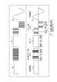
- FIG. 1 shows an example of schematic structure of a power conversion system. It is an example of the circuit diagram which shows the detail of the power conversion system which paid attention only to the storage battery in FIG.
- It is a wave form diagram (horizontal writing) which shows simply the characteristic of operation of a DC / DC converter and an inverter in a minimum switching conversion system.
- It is a wave form diagram (vertical writing) which shows simply the feature of operation of a DC / DC converter and an inverter in a minimum switching conversion system.
- It is a voltage control block diagram on the high voltage side of the second DC / DC converter.
- FIG. 3 is a circuit diagram in which a second DC / DC converter is deleted from FIG. 2 for comparison. It is a wave form diagram of the system
- the charge / discharge current flowing in the storage battery becomes a pulsating flow.
- the reactive current resulting from the fact that the voltage of the DC bus is not a constant voltage cannot be completely absorbed by the electrolytic capacitor connected in parallel to the storage battery. This does not cause a problem immediately, but when the constant DC current and the pulsating current are compared, the latter has a larger loss caused by the internal resistance of the storage battery.
- an object of the present disclosure is to improve versatility for various storage batteries and reduce loss of the storage battery in a power conversion system.
- the gist of the embodiment of the present invention includes at least the following.
- This is a power conversion system in which a DC power supply circuit and a power conditioner are connected to each other, and the power conditioner is provided between a first DC power supply circuit and a DC bus.
- a DC / DC converter, and an inverter that is provided between the DC bus and the AC circuit, and that performs a switching operation alternately with the first DC / DC converter in the AC half cycle
- the DC power supply circuit includes a storage battery, and a bidirectional second DC / DC converter provided between the storage battery and the first DC / DC converter and including a DC reactor, It is a power conversion system which has a control part which performs control which makes the electric current which flows into the said DC reactor of 2 DC / DC converters into a constant value.
- the voltage can be stepped up and down, and the applicable range of voltage is widened. Therefore, various storage batteries having different output voltages can be connected to the power conditioner via the second DC / DC converter. Further, in the minimum switching conversion method in which the first DC / DC converter and the inverter alternately have a switching pause period in the AC half cycle, the current of the pulsating waveform is on the low voltage side of the first DC / DC converter.
- the control unit attempts to flow, the control unit controls the current flowing through the DC reactor of the second DC / DC converter to a constant value, for example, the low voltage side (second DC / DC converter) of the first DC / DC converter.
- a constant value for example, the low voltage side (second DC / DC converter) of the first DC / DC converter.
- the control unit sets the high voltage side voltage target value to a low voltage as an operation amount of the high voltage side voltage feedback control of the second DC / DC converter.
- a value averaged at a constant cycle is defined as a charge / discharge current target value
- the high voltage side of the second DC / DC converter is set to a constant voltage. You may control to.
- an averaged flat direct current can be passed to the low voltage side of the second DC / DC converter. That is, the second DC / DC converter can control the charge / discharge current of the storage battery to a constant current that is not a pulsating current waveform.
- T is the period
- igdc_ref is the charge / discharge current target value
- ipwm_ref_pi_vdc is the manipulated variable
- vdc_ref is the voltage target value
- vgdc is the detected voltage value
- the control unit averages a compensation amount based on a voltage feedback on the low voltage side of the first DC / DC converter in an AC half cycle.
- a current target value of a direct current reactor included in the first DC / DC converter may be determined, and the low voltage side of the first DC / DC converter may be controlled to a constant voltage.
- an averaged flat direct current can be flowed to the low voltage side of the first DC / DC converter. Therefore, the voltage on the low voltage side of the first DC / DC converter can be set to a constant value.
- the power conditioner is a composite power conditioner that is also connected to one or a plurality of photovoltaic power generation panels, and the second DC The / DC converter may output a voltage matching the highest voltage among the output voltages of the photovoltaic power generation panel to the high voltage side.
- the power conditioner optimizes the operation of the minimum switching conversion method. be able to.
- the power conditioner of (4) is a composite power conditioner connected to one or a plurality of photovoltaic power generation panels, and the first DC / DC converter includes the sunlight.
- a voltage that matches the highest voltage among the output voltages of the power generation panel may be output to the low voltage side.
- the second DC / DC The DC converter may perform communication for receiving a voltage target value to be constant from the power conditioner.
- the output voltage target value on the high voltage side can be notified from the power conditioner to the second DC / DC converter by communication.
- the output voltage target value can be notified to the second DC / DC converter when the voltage matching the highest voltage among the output voltages of the photovoltaic power generation panel is used as the voltage of the DC bus.
- the 2nd DC / DC converter can output the voltage which corresponds with the highest voltage among the output voltages of a photovoltaic power generation panel to the high voltage side.
- the first DC / DC converter has an increased switching stop period, which contributes to optimization of the operation of the minimum switching conversion method.
- the first DC / DC converter when the first DC / DC converter controls its low voltage side to a constant voltage, the first DC / DC converter You may make it perform communication which transmits an output electric power command value to a said 2nd DC / DC converter. In this case, by notifying the second DC / DC converter of the output power command value, the second DC / DC converter can control the charge / discharge current to a constant current based on the output power command value.
- a DC power supply circuit and a power conditioner are connected to each other, and the power conditioner is a first DC provided between the DC power supply circuit and the DC bus.
- a DC / DC converter and an inverter provided between the DC bus and the AC circuit, and the DC power supply circuit is provided between the storage battery, the storage battery and the first DC / DC converter.
- a control method using a power conversion system having a bidirectional DC / DC converter including a direct current reactor as an execution subject The second DC / DC converter boosts the voltage of the storage battery to a voltage on the low voltage side of the first DC / DC converter, or steps down the voltage in the opposite direction, so that the first DC / DC converter
- the inverter performs a switching operation while alternately having a pause period in an AC half cycle, and performs control to set the current flowing through the DC reactor of the second DC / DC converter to a constant value.
- the second DC / DC converter can act as a voltage mediator between the two. it can. Therefore, various storage batteries having different output voltages can be connected to the power conditioner via the second DC / DC converter. Further, in the minimum switching conversion method in which the first DC / DC converter and the inverter alternately have a switching pause period in the AC half cycle, the current of the pulsating waveform is on the low voltage side of the first DC / DC converter.
- the control is performed so that the current flowing through the DC reactor of the second DC / DC converter is a constant value
- the low voltage side of the first DC / DC converter (the high voltage of the second DC / DC converter is By performing the control in such a manner that the voltage on the voltage side) is a constant value, only a direct current flows through the storage battery, and no current with a pulsating waveform flows. Thereby, the loss by the internal resistance of a storage battery can be suppressed, deterioration of a storage battery can be delayed, and the performance of a storage battery can fully be exhibited.
- the power conversion system can also be expressed as follows, separately from (1). That is, this is a power conversion system in which a DC power supply circuit and a power conditioner are connected to each other, and the power conditioner is connected to a first DC / DC provided between the DC power supply circuit and a DC bus. A DC converter, and an inverter provided between the DC bus and the AC circuit, and performing switching operation alternately with a pause period in the AC half cycle with the first DC / DC converter.
- the power supply circuit includes a storage battery, and a bidirectional second DC / DC converter that is provided between the storage battery and the first DC / DC converter and includes a direct current reactor.
- a conversion system includes a capacitor provided between the first DC / DC converter and the second DC / DC converter, and the first DC / DC converter.
- the pulsating component and the direct current component of the pulsating current flowing through the capacitor the pulsating component is supplied by the capacitor, and the direct current component is supplied by the second DC / DC converter.
- a control unit that controls the current flowing through the DC reactor of the DC converter to have a constant value.
- FIG. 1 is a diagram illustrating an example of a schematic configuration of a power conversion system 100.
- the power conversion system 100 is configured by connecting a plurality of types of DC power supplies to the composite power conditioner 1 and can be connected to the commercial power system 3.
- a consumer's load 4 is connected to an AC power line 5 between the commercial power system 3 and the power conditioner 1.
- three photovoltaic power generation panels 7A, 7B, and 7C are connected to the composite power conditioner 1.
- the “three” is only an example.
- a storage battery 6 is connected to the power conditioner 1 via a bidirectional DC / DC converter 8. Specifically, the low voltage side (left side in the figure) of the DC / DC converter 8 is connected to the storage battery 6, and the high voltage side (right side in the figure) is connected to the power conditioner 1.
- the voltage of the commercial power system 3 is AC202V
- the peak value (peak value) in that case is about 286V
- the voltage input to a DC converter (not shown) and subjected to MPPT (Maximum Power Point Tracking) control is DC 250V.
- This voltage becomes the DC bus voltage in the power conditioner 1.
- the voltage of the storage battery 6 is DC39 to 53V. Therefore, the voltage of the storage battery 6 is boosted by the DC / DC converter 8 and further boosted to DC 250 V by the DC / DC converter 11 (FIG. 2) in the power conditioner 1.
- the basic effect of providing the DC / DC converter 8 is that, even if there is a large difference in input / output voltage between the power conditioner 1 and the storage battery 6, it is possible to increase / decrease the voltage, and the application range of the voltage is wide. It is to become. Therefore, various storage batteries 6 having different output voltages can be connected to the power conditioner 1 via the DC / DC converter 8.
- FIG. 2 is an example of a circuit diagram showing details of the power conversion system 100 focusing only on the storage battery 6 in FIG.
- a power conditioner 1 and a DC / DC converter 8 are provided between the AC circuit 5 and the storage battery 6.
- the AC electric circuit 5 is provided with a power monitor 30 for the AC electric circuit 5.
- the storage battery 6 is actually configured as a power storage system, not just a battery, and has a monitor function for monitoring its own state and a communication function for exchanging information with the outside (details will be described later). .
- the power conditioner 1 is connected to a DC / DC converter 11, a high voltage side DC bus 12, an inverter 13 connected to the DC bus 12, and a low voltage side of the DC / DC converter 11 as main circuit elements.
- the low voltage side capacitor 14, the intermediate capacitor 15 connected to the DC bus 12, the AC reactor 16, and the AC side capacitor 17 are provided.
- the high voltage side of the DC / DC converter 8 is connected to the low voltage side of the DC / DC converter 11.
- the inverter 13 is connected to the high voltage side of the DC / DC converter 11.
- the DC / DC converter 11 is connected to a DC reactor 11L as circuit elements constituting a chopper circuit, a high-side switching element Q3 and a diode d3 connected in antiparallel, and a low-side switching element Q4 and antiparallel. And a diode d4.
- the inverter 13 is a full-bridge connection of switching elements Q5, Q6, Q7, and Q8. Diodes d5, d6, d7, and d8 are connected in antiparallel to switching elements Q5, Q6, Q7, and Q8, respectively.
- Both the DC / DC converter 8 and the DC / DC converter 11 can be used in both directions.
- the storage battery 6 When the storage battery 6 is discharged, it becomes a step-up chopper, and when the storage battery 6 is charged, it becomes a step-down chopper.
- the inverter 13 can not only perform conversion from direct current to alternating current but also be a bidirectional DC / AC converter, and can also perform conversion from alternating current to direct current in the reverse direction.
- switching elements Q3 to Q8 for example, illustrated IGBT (Insulated Gate Bipolar Transistor) or MOSFET (Metal-Oxide Semiconductor Field-Effect Transistor) can be used.
- the AC reactor 16 and the AC side capacitor 17 constitute a filter circuit and prevent high frequency components generated by the inverter 13 from leaking into the AC circuit 5.
- a voltage sensor 18 for detecting the voltage across the low-voltage side capacitor 14 a current sensor 19 for detecting the current flowing through the DC reactor 11 ⁇ / b> L, and the voltage of the DC bus 12, that is, the voltage across the intermediate capacitor 15.
- a current sensor 21 for detecting the current flowing through the AC reactor 16 and a voltage sensor 22 for detecting the voltage across the AC capacitor 17.
- the detection output signal of each sensor is sent to the control unit 10.
- Control unit 10 controls on / off of switching elements Q3, Q4, Q5 to Q8.
- the control unit 10 includes, for example, a computer, and a necessary control function is realized by the software (computer program) being executed by the computer.
- the software is stored in a storage device (not shown) of the control unit.
- the DC / DC converter 8 includes a DC reactor 8L as a chopper circuit, a high-side switching element Q1 and a diode d1 connected in reverse parallel, a low-side switching element Q2 and a diode d2 connected in reverse parallel. And.
- a low voltage side capacitor 81 is connected to the low voltage side of the DC / DC converter 8, and a high voltage side capacitor 82 is connected to the high voltage side.
- the switching elements Q1, Q2 for example, an IGBT or a MOSFET can be used.
- a voltage sensor 83 for detecting the voltage across the capacitor 81
- a current sensor 84 for detecting the current flowing through the DC reactor 8L
- a voltage sensor 85 for detecting the voltage across the high-voltage side capacitor 82. Is provided. The detection output signal of each sensor is sent to the control unit 80.
- Control unit 80 controls on / off of switching elements Q1, Q2.
- the control unit 80 includes, for example, a computer, and realizes necessary control functions by causing the computer to execute software (computer program).
- the software is stored in a storage device (not shown) of the control unit.
- the DC / DC converter 8 and the storage battery 6 constitute a DC power supply circuit 9. That is, the power conversion system 100 is configured by connecting the DC power supply circuit 9 and the power conditioner 1 to each other.
- the power conditioner 1 is provided between the first DC / DC converter 11 provided between the DC power supply circuit 9 and the DC bus 12, the DC bus 12 and the AC circuit 5, and is connected to the AC half cycle.
- the first DC / DC converter 11 and the inverter 13 that performs a switching operation alternately with a pause period are provided.
- the second DC / DC converter 8 of the DC power supply circuit 9 is a bidirectional converter that is provided between the storage battery 6 and the first DC / DC converter 11 and includes a DC reactor 8L. .
- control unit 10 and the control unit 80 have a communication function, and the control unit 10 can perform necessary communication with the power monitor 30 and the control unit 80.
- the control unit 80 can perform necessary communication with the storage battery 6 and the control unit 10.
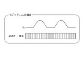
- FIG. 3 and FIG. 4 are waveform diagrams simply showing the characteristics of the operation of the DC / DC converter 11 and the inverter 13 in the minimum switching conversion method. Although both figures show the same contents, FIG. 3 is displayed horizontally so that the amplitude relationship from DC input to AC output is easy to see, and FIG. 4 is particularly displayed vertically so that the timing of control is easy to see. ing.
- the upper part of FIG. 3 and the left column of FIG. 4 are waveform diagrams representing traditional switching control that is not the minimum switching conversion method, for comparison. Further, the lower part of FIG. 3 and the right column of FIG. 4 are waveform diagrams showing the operation of the minimum switching conversion method.
- the output of the DC / DC converter with respect to the input DC voltage V dc is a pulse train of equal intervals higher than V dc. Is. This output is smoothed by the intermediate capacitor, the DC bus, appears as voltage V O.
- the inverter performs PWM (Pulse Width Modulation) controlled switching while inverting the polarity in a half cycle. As a result, a sinusoidal AC voltage V ac is obtained through final smoothing.
- the DC / DC converter 11 corresponds to the comparison result between the absolute value of the instantaneous value of the voltage target value V ac of the AC waveform and the input DC voltage V dc.
- the inverter 13 operate. That is, when V ac ⁇ V dc (or V ac ⁇ V dc ) in the absolute value of the voltage target value V ac , the DC / DC converter 11 stops (“ST” in the figure), and V ac ⁇ V dc When (or V ac > V dc ), the DC / DC converter 11 performs a boosting operation (“OP” in the figure).
- the output of the DC / DC converter 11 is smoothed by the intermediate capacitor 15, the DC bus 12, it appears as voltage V O shown.
- the intermediate capacitor 15 has a small capacity (for example, a microfarad level). Therefore, a part of the waveform around the peak of the absolute value of the AC waveform remains without being smoothed. That is, the smoothing works to the extent that the trace of the high frequency switching by the DC / DC converter 11 is erased, but the intermediate capacitor 15 has a small capacity so that the low frequency about twice the commercial frequency cannot be smoothed. It has become.
- the inverter 13 performs high-frequency switching when V ac ⁇ V dc (or V ac ⁇ V dc ) according to the comparison result between the absolute value of the voltage target value V ac and the DC voltage V dc. If it is performed (“OP” in the figure) and V ac ⁇ V dc (or V ac > V dc ), high-frequency switching is stopped (“ST” in the figure). When the high frequency switching is stopped, the inverter 13 selects one of the switching elements Q5 and Q8 being on, Q6 and Q7 being off, and the switching elements Q5 and Q8 being off and Q6 and Q7 being on. By doing so, only necessary polarity inversion is performed. The output of the inverter 13 is smoothed by the AC reactor 16 and the AC side capacitor 17, and a desired AC output is obtained.
- the DC / DC converter 11 and the inverter 13 are alternately performing high-frequency switching operations, and when the DC / DC converter 11 is performing a boosting operation.
- the inverter 13 stops high-frequency switching and performs only necessary polarity inversion with respect to the voltage of the DC bus 12. Conversely, when the inverter 13 performs high-frequency switching operation, the DC / DC converter 11 stops and the voltage across the low-voltage side capacitor 14 appears on the DC bus 12 via the DC reactor 11L and the diode d3.
- FIG. 5 is a voltage control block diagram on the high voltage side of the DC / DC converter 8.
- the control execution subject is the control unit 80.
- the control unit 80 uses a voltage detection value vdc on the high voltage side detected by the voltage sensor 85 (FIG. 2) as a control amount, and calculates an error amount dvdc between the voltage target value vdc_ref on the high voltage side and the control amount vdc. calculate.
- the control unit 80 passes the error amount dvdc through the PI compensator and calculates the operation amount ipwm_ref_pi_vdc.
- the manipulated variable ipwm_ref_pi_vdc calculated in the voltage control block diagram on the high voltage side physically means the current input / output to / from the high voltage side capacitor 82 of the DC / DC converter 8. Therefore, in calculating the current target value of the DC reactor 8L in the DC / DC converter 8, the voltage target value vdc_ref on the high voltage side is divided by the voltage detection value vgdc on the storage battery side detected by the voltage sensor 83 (FIG. 2). The value is multiplied by the manipulated variable ipwm_ref_pi_vdc to convert it into a current target value of the DC reactor 8L.
- the converted value is averaged at a constant period T longer than the PWM period to obtain the current target value igdc_ref of the DC reactor 8L. Since the purpose is to remove the AC component, T is set to an AC cycle (for example, 1/60 [seconds]) or 1/2 thereof.
- FIG. 6 is a current control block diagram of the DC reactor 8L in the DC / DC converter 8.
- the control unit 80 calculates an error amount digdc from the target current value igdc_ref of the DC reactor 8L using the current detection value igdc of the DC reactor 8L detected by the current sensor 84 as a control amount. Then, the control unit 80 passes the error amount digdc through the PI compensator, adds the voltage detection value vgdc on the storage battery side as disturbance compensation to the calculation result, and further divides by the voltage detection value vdc on the high voltage side. Thereby, the operation amount th_sw is calculated. The duty of the switching elements Q1, Q2 of the DC / DC converter 8 is determined using this manipulated variable.
- the DC / DC converter 8 outputs to the high voltage side a voltage that matches the highest voltage among the output voltages of the photovoltaic power generation panels 7A, 7B, and 7C.
- the switching stop period of the DC / DC converter 11 increases. To do. This contributes to optimization of the operation of the minimum switching conversion method in the power conditioner 1.
- the DC / DC converter 11 can output a voltage matching the highest voltage among the output voltages of the photovoltaic power generation panels 7A, 7B, and 7C to the low voltage side.
- FIG. 7 is a circuit diagram in which the DC / DC converter 8 is omitted from FIG. 2 for comparison.
- FIG. 8 is a waveform diagram of the system current (frequency is 50 Hz) detected by the current sensor 21 in the circuit of FIG.
- FIG. 9 is a waveform diagram of the system voltage (frequency is 50 Hz) detected by the voltage sensor 22 in the circuit of FIG.
- FIG. 10 is a waveform diagram of the charging current to the storage battery 6 detected by the current sensor 19 in the circuit of FIG.
- the charging current is pulsating
- the average value is 29.6 [A]
- the peak value viewed from 0 is 68 [A]
- the pulsating cycle is 1 of the alternating cycle. / 2.
- the waveform diagram of the system current (frequency is 50 Hz) detected by the current sensor 21 and the waveform diagram of the system voltage (frequency is 50 Hz) detected by the voltage sensor 22 are the same as those in FIGS. 8 and 9, respectively. .
- FIG. 11 is a waveform diagram of a voltage at an interconnection point between the DC / DC converter 8 detected by the voltage sensors 18 and 85 and the power conditioner 1.
- the scale is enlarged in the vertical axis direction.
- the average value is 200 [V]
- the peak-to-peak value is 6 [V].
- FIG. 12 is a waveform diagram of the charging current to the storage battery 6 detected by the current sensor 84 in the circuit of FIG. As shown in the figure, it can be seen that the charging current is in a state that can be said to be a direct current, although there are extremely small fluctuations.
- the average value of the current is 30.2 [A]
- the peak-to-peak value is 1.8 [A].
- the charging current to the storage battery 6 becomes DC by providing the DC / DC converter 8 between the storage battery 6 and the power conditioner 1 and performing predetermined control.
- the discharge current is also a direct current when the storage battery 6 is discharged.
- the loss due to the internal resistance of the storage battery 6 is reduced to 2/3 as compared with the case where charging / discharging is performed with the pulsating current having the same average value.
- the control unit 80 of the DC / DC converter 8 can act as an intermediary for communication. For example, if various communication interface functions are installed in the DC / DC converter 8 for communication with the storage battery 6, even if the storage battery 6 having various communication specifications by the storage battery manufacturer is used, for example, the DC / DC converter 8 can be communicated. From the viewpoint of the power conditioner 1, as long as communication with the DC / DC converter 8 is possible, the communication specification of the storage battery 6 is not limited, which is practically convenient.
- FIG. 13 is a diagram showing an example of information signal transmission / reception.
- Signals S 1 and S 2 are transmitted and received between the DC / DC converter 8 and the storage battery 6.
- Signals S3 and S4 are transmitted and received between the power conditioner 1 and the DC / DC converter 8.
- Signals S5 and S6 are transmitted and received between the power monitor 30 and the power conditioner 1.
- PCS is an abbreviation that means a power conditioner
- PV is a solar power generation panel
- DC / DC is a DC / DC converter 8.
- S1 Operation start instruction
- operation stop instruction S2: Storage battery voltage, cell voltage, system operation information, current
- SOC State of Charge
- S3 DC / DC operation instruction
- PCS operation status S4: DC / DC operation mode, request state to PCS
- storage battery operation information S5: PCS operation instruction, storage battery operation instruction, storage battery charge / discharge target value, PCS output power maximum value
- S6 PCS operation content, storage battery operation content, PCS output power, each PV generated power, storage battery charge / discharge power, storage battery capacity (SOC), PCS state, storage battery state, log code
- the current flowing through the DC reactor 8L of the second DC / DC converter 8 is set to a constant value (in other words, the voltage on the high voltage side of the DC / DC converter 8 is set to a constant value).
- Control only the direct current flows through the storage battery 6 and the current of the pulsating waveform does not flow. Thereby, the loss by the internal resistance of the storage battery 6 can be suppressed, the deterioration of the storage battery 6 can be delayed, and the performance of the storage battery 6 can be exhibited sufficiently.
- the second DC / DC converter 8 controls its high voltage side to a constant voltage
- the second DC / DC converter 8 receives a voltage target value to be made constant from the power conditioner 1. I do.
- the output voltage target value on the high voltage side can be notified from the power conditioner 1 to the second DC / DC converter 8.
- the output voltage target value can be notified to the second DC / DC converter 8 when the voltage matching the highest voltage among the output voltages of the photovoltaic power generation panel is used as the voltage of the DC bus 12.
- the 2nd DC / DC converter 8 can output the voltage which corresponds with the highest voltage among the output voltages of a photovoltaic power generation panel to the high voltage side.
- the first DC / DC converter 11 has an increased switching stop period, which contributes to optimization of the operation of the minimum switching conversion method.
- the power conversion system (including its control method) of the second embodiment will be described.
- the circuit configuration and minimum switching conversion are the same as in the first embodiment.
- the constant current control of the second DC / DC converter 8 in the first embodiment is “subordinate”, and the DC / DC converter 11 in the power conditioner 1 is led by the low DC / DC 11. Constant voltage control for controlling the voltage side to a constant voltage is performed.
- I dc Current detection value of DC reactor 11
- I * dc Current target value of DC reactor 11
- V dc Storage battery unit input voltage detection value (detection value of voltage sensor 18)
- V * dc storage battery unit input voltage target value
- Cdc combined capacity of capacitors 14 and 82
- I * ac AC output current target value
- Cac Capacitance of the AC side capacitor 17
- I * inv Current target value of the AC reactor 16
- V * inv Voltage target value Rinv on the AC side of the inverter 13: Resistance of the inverter 13 Component (mainly resistance component of AC reactor 16)
- L inv Inductance
- C o of AC reactor 16 Capacity
- V o of intermediate capacitor 15 Voltage detection value of intermediate capacitor 15 (detection value of voltage sensor 20)
- V * o Voltage target value Rdc of the intermediate capacitor 15: Resistance component of the DC / DC
- the current detection value I dc of the DC reactor 11L can be written as in equation (1) by the combined capacity C dc and the storage battery unit input voltage detection value V dc .
- T is an AC half cycle
- K dc is a compensation coefficient
- the current target value of the DC reactor 11L is (the power on the DC side of the inverter 13) + (the charge / discharge power of the intermediate capacitor 15), and the voltage between the collector and the emitter of the switching element Q4 (this is the case of the IGBT). In the case of a MOSFET, it can be obtained by dividing by the voltage between the drain and source.
- the collector of the switching element Q4 - emitter voltage can be calculated by considering the voltage drop due to the inductance L dc DC reactor 11L and a resistance component from the storage battery unit input voltage detection value V dc. That is, the current target value of the DC reactor 11L is expressed by the following equation (4).
- equation (5) is obtained.
- the charging / discharging power of the intermediate capacitor 15 and the voltage drop of the DC reactor 11L are 0 when taking the average in the AC half cycle, and can be written as shown in Equation (6).
- Symbol ⁇ > represents an average value.
- the current target value I * inv of the AC reactor 16 is expressed by the equation (7) by the AC output current target value I * ac and the charge / discharge current of the AC capacitor Cac .
- the voltage target value V * inv of the inverter 13 is expressed by the following equation (9) in consideration of the voltage drop due to the resistance component and the inductance component of the AC reactor 16 in the AC system voltage detection value Vac .
- FIG. 14A and 14B are diagrams illustrating two examples of the switching operation of the DC / DC converter 11.
- the voltage target value V dc * of the intermediate capacitor 15 is set to a constant voltage, but when the voltage value that is the maximum value of the generated voltage during solar power generation is V pv-max , V dc * ⁇ V pv-max If there is, the minimum voltage of the voltage V o of the intermediate capacitor 15 becomes V pv-max , so that the DC / DC converter 11 always performs the step-up or step-down operation, and the conversion efficiency is not reduced without the minimum switching conversion.
- Invite (FIG. 14A). For this reason, by setting the set value of V dc * to V pv-max , the useless boosting operation of the DC / DC converter 11 is eliminated, leading to improved conversion efficiency (FIG. 14B).
- the value obtained by averaging the compensation amount based on the voltage feedback on the low voltage side of the first DC / DC converter 11 in the half cycle of the AC is the first DC / DC converter 11.
- the current target value of the DC reactor 11L is determined, and the low voltage side of the first DC / DC converter 11 can be controlled to a constant voltage.
- the second DC / DC converter 8 is led by the first DC / DC converter 11 by performing constant voltage control in which the voltage on the low voltage side of the first DC / DC converter 11 is a constant value.
- the current flowing through the second DC / DC converter 8 can be made constant.
- the first DC / DC converter 11 controls its low voltage side to a constant voltage
- the first DC / DC converter 11 transmits an output power command value to the second DC / DC converter 8.
- Communication can be performed.
- the second DC / DC converter 8 can control the charge / discharge current to a constant current based on the output power command value. it can.
Abstract
Provided is a power conversion system that is formed by connecting a direct-current power supply circuit and a power conditioner to each other. The power conditioner is equipped with: a first DC/DC converter that is provided between the direct-current power supply circuit and a DC bus; and an inverter that is provided between the DC bus and an alternating-current electrical path, and that performs a switching operation while having an idle period that alternates with that of the first DC/DC converter within an alternating-current half cycle. The direct-current power supply circuit includes a storage battery and a bidirectional second DC/DC converter that is provided between the storage battery and the first DC/DC converter and that includes a direct-current reactor. The direct-current power supply circuit has a control unit that performs control to make a current that flows to the direct-current reactor of the second DC-DC converter have a constant value.
Description
本発明は、電力変換システム及びその制御方法に関する。
本出願は、2016年1月18日出願の日本出願第2016-006999号に基づく優先権を主張し、前記日本出願に記載された全ての記載内容を援用するものである。 The present invention relates to a power conversion system and a control method thereof.
This application claims priority based on Japanese Patent Application No. 2016-006999 filed on Jan. 18, 2016, and incorporates all the description content described in the above Japanese application.
例えば太陽光発電用のパワーコンディショナ(電力変換装置)は、直流の発電電力を交流に変換して、商用電力系統へ系統連系する運転を行う。伝統的なパワーコンディショナの変換動作によれば、発電した電圧を、交流側のピーク電圧より高い一定電圧まで昇圧回路で昇圧した後、インバータで交流電圧に変換している。この場合、昇圧回路及びインバータは、常時高速なスイッチング動作を行っている。
For example, a power conditioner (power conversion device) for photovoltaic power generation performs an operation of converting a direct-current generated power into an alternating current and grid-connecting to a commercial power system. According to the conversion operation of a conventional power conditioner, the generated voltage is boosted by a booster circuit to a constant voltage higher than the peak voltage on the AC side, and then converted into an AC voltage by an inverter. In this case, the booster circuit and the inverter always perform a high-speed switching operation.
一方、かかるパワーコンディショナでは、変換効率を向上させることが重要である。そこで、直流側の電圧と交流側の瞬時電圧の絶対値とを常に比較して、昇圧回路については昇圧が必要な期間のみスイッチング動作させ、インバータについては降圧が必要な期間のみスイッチング動作させる、という制御(以下、最小スイッチング変換方式という。)が提案されている(例えば特許文献1,2参照。)。このような最小スイッチング変換方式によって昇圧回路及びインバータにスイッチング動作の休止期間ができると、その分、スイッチング損失等が低減されるので、変換効率を向上させることができる。
On the other hand, in such a power conditioner, it is important to improve the conversion efficiency. Therefore, the DC side voltage is always compared with the absolute value of the instantaneous voltage on the AC side, and the booster circuit is switched only during the period that requires boosting, and the inverter is switched only during the period that requires stepping down. Control (hereinafter referred to as a minimum switching conversion method) has been proposed (see, for example, Patent Documents 1 and 2). If the boosting circuit and the inverter have a pause period of the switching operation by such a minimum switching conversion method, the switching loss and the like are reduced accordingly, so that the conversion efficiency can be improved.
また、近年、太陽電池と蓄電池という2種類の直流電源を用いて、直流/交流の電力変換を行う、いわゆる複合型のパワーコンディショナが提案されている(例えば、特許文献3,4参照。)。このような複合型のパワーコンディショナは、1又は複数の太陽光発電パネルからの出力と、蓄電池の出力とを1台のパワーコンディショナに繋ぎ込むことができる。パワーコンディショナ内には各電源の必要に応じてDC/DCコンバータ(チョッパ回路)、及び、インバータが搭載され、商用電力系統との系統連系運転を行うことができる。
In recent years, so-called composite power conditioners that perform DC / AC power conversion using two types of DC power sources, that is, a solar battery and a storage battery, have been proposed (see, for example, Patent Documents 3 and 4). . Such a composite type power conditioner can connect the output from one or a plurality of photovoltaic power generation panels and the output of the storage battery to one power conditioner. A DC / DC converter (chopper circuit) and an inverter are mounted in the power conditioner as necessary for each power source, and system interconnection operation with the commercial power system can be performed.
一表現による本発明は、直流電源回路とパワーコンディショナとを互いに接続して成る電力変換システムであって、前記パワーコンディショナは、前記直流電源回路とDCバスとの間に設けられた第1のDC/DCコンバータと、前記DCバスと交流電路との間に設けられ、交流半サイクル内で前記第1のDC/DCコンバータと交互に休止期間を有しつつスイッチング動作するインバータと、を備え、前記直流電源回路は、蓄電池と、前記蓄電池と前記第1のDC/DCコンバータとの間に設けられ、直流リアクトルを含む、双方向性の第2のDC/DCコンバータと、を備えたものであり、前記第2のDC/DCコンバータの前記直流リアクトルに流れる電流を一定値とする制御を行う制御部を有する電力変換システムである。
The present invention according to one expression is a power conversion system in which a DC power supply circuit and a power conditioner are connected to each other, wherein the power conditioner is provided between a first DC power supply circuit and a DC bus. A DC / DC converter, and an inverter that is provided between the DC bus and the AC circuit, and that performs a switching operation alternately with the first DC / DC converter in the AC half cycle while having a pause period. The DC power supply circuit includes a storage battery, and a bidirectional second DC / DC converter provided between the storage battery and the first DC / DC converter and including a DC reactor. And a power conversion system having a control unit that controls the current flowing through the DC reactor of the second DC / DC converter to have a constant value.
また、他の観点からは、直流電源回路とパワーコンディショナとを互いに接続して成り、前記パワーコンディショナは、前記直流電源回路とDCバスとの間に設けられた第1のDC/DCコンバータと、前記DCバスと交流電路との間に設けられたインバータとを有し、前記直流電源回路は、蓄電池と、前記蓄電池と前記第1のDC/DCコンバータとの間に設けられ、直流リアクトルを含む、双方向性の第2のDC/DCコンバータとを有するものである電力変換システムを実行主体とした、その制御方法であって、前記第2のDC/DCコンバータは、前記蓄電池の電圧を前記第1のDC/DCコンバータの低電圧側の電圧に昇圧し、又は、その逆方向に降圧し、前記第1のDC/DCコンバータと、前記インバータとは、交流半サイクル内で交互に休止期間を有しつつスイッチング動作し、前記第2のDC/DCコンバータの前記直流リアクトルに流れる電流を一定値とする制御を行う、電力変換システムの制御方法である。
From another point of view, a DC power supply circuit and a power conditioner are connected to each other, and the power conditioner is a first DC / DC converter provided between the DC power supply circuit and a DC bus. And an inverter provided between the DC bus and the AC circuit, and the DC power supply circuit is provided between the storage battery, the storage battery and the first DC / DC converter, and a DC reactor. Including a bidirectional second DC / DC converter, and a control method thereof, wherein the second DC / DC converter is a voltage of the storage battery. Is boosted to a voltage on the low voltage side of the first DC / DC converter, or in the opposite direction, the first DC / DC converter and the inverter Switching operation while having a rest period alternately in Le performs control for a current flowing through the DC reactor of the second DC / DC converter to a constant value, a method of controlling a power conversion system.
[本開示が解決しようとする課題]
複合型のパワーコンディショナにおいては、特に、各種の蓄電池を接続したい現実的なニーズがある。ところが、色々な種類の蓄電池を使用することを想定すると、その端子電圧は広範囲に及ぶ。現実にはさらに、想定した範囲外の電圧の蓄電池を使用したい場合もあり、現状ではパワーコンディショナ側の対応が十分ではない。 [Problems to be solved by the present disclosure]
In the hybrid power conditioner, there is a practical need to connect various storage batteries. However, assuming that various types of storage batteries are used, the terminal voltage ranges widely. In reality, there is a case where it is desired to use a storage battery having a voltage outside the assumed range, and the power conditioner side is not sufficient at present.
一方、蓄電池を直流電源として最小スイッチング変換方式を適用した場合、蓄電池に流れる充放電電流が脈流になる。これは、DCバスの電圧が一定電圧ではないことに起因する無効電流を、蓄電池に並列接続された電解コンデンサによって完全には吸収できないからである。このことは、直ちに問題となることではないが、一定値の直流電流と脈流電流とを比べると、後者の方が、蓄電池の内部抵抗によって発生する損失が大きい。
On the other hand, when the minimum switching conversion method is applied using the storage battery as a DC power supply, the charge / discharge current flowing in the storage battery becomes a pulsating flow. This is because the reactive current resulting from the fact that the voltage of the DC bus is not a constant voltage cannot be completely absorbed by the electrolytic capacitor connected in parallel to the storage battery. This does not cause a problem immediately, but when the constant DC current and the pulsating current are compared, the latter has a larger loss caused by the internal resistance of the storage battery.
かかる課題に鑑み、本開示は、電力変換システムにおいて、各種の蓄電池に対する汎用性を高め、かつ、蓄電池の損失を低減することを目的とする。
In view of such a problem, an object of the present disclosure is to improve versatility for various storage batteries and reduce loss of the storage battery in a power conversion system.
[本開示の効果]
本開示によれば、電力変換システムにおいて、各種の蓄電池に対する汎用性を高め、かつ、蓄電池の損失を低減することができる。 [Effects of the present disclosure]
According to the present disclosure, in the power conversion system, versatility with respect to various storage batteries can be improved, and loss of the storage batteries can be reduced.
本開示によれば、電力変換システムにおいて、各種の蓄電池に対する汎用性を高め、かつ、蓄電池の損失を低減することができる。 [Effects of the present disclosure]
According to the present disclosure, in the power conversion system, versatility with respect to various storage batteries can be improved, and loss of the storage batteries can be reduced.
[実施形態の要旨]
本発明の実施形態の要旨としては、少なくとも以下のものが含まれる。 [Summary of Embodiment]
The gist of the embodiment of the present invention includes at least the following.
本発明の実施形態の要旨としては、少なくとも以下のものが含まれる。 [Summary of Embodiment]
The gist of the embodiment of the present invention includes at least the following.
(1)これは、直流電源回路とパワーコンディショナとを互いに接続して成る電力変換システムであって、前記パワーコンディショナは、前記直流電源回路とDCバスとの間に設けられた第1のDC/DCコンバータと、前記DCバスと交流電路との間に設けられ、交流半サイクル内で前記第1のDC/DCコンバータと交互に休止期間を有しつつスイッチング動作するインバータと、を備え、前記直流電源回路は、蓄電池と、前記蓄電池と前記第1のDC/DCコンバータとの間に設けられ、直流リアクトルを含む、双方向性の第2のDC/DCコンバータと、を備え、前記第2のDC/DCコンバータの前記直流リアクトルに流れる電流を一定値とする制御を行う制御部を有する電力変換システムである。
(1) This is a power conversion system in which a DC power supply circuit and a power conditioner are connected to each other, and the power conditioner is provided between a first DC power supply circuit and a DC bus. A DC / DC converter, and an inverter that is provided between the DC bus and the AC circuit, and that performs a switching operation alternately with the first DC / DC converter in the AC half cycle, The DC power supply circuit includes a storage battery, and a bidirectional second DC / DC converter provided between the storage battery and the first DC / DC converter and including a DC reactor, It is a power conversion system which has a control part which performs control which makes the electric current which flows into the said DC reactor of 2 DC / DC converters into a constant value.
このように構成された電力変換システムでは、パワーコンディショナと蓄電池との間に入出力電圧の大きな差があっても、昇降圧が可能となり、しかも電圧の適用範囲が広くなる。従って、出力電圧の異なる各種の蓄電池を第2のDC/DCコンバータ経由でパワーコンディショナに接続することができる。また、第1のDC/DCコンバータとインバータとが交流半サイクル内で交互にスイッチングの休止期間を有する最小スイッチング変換方式では、脈流波形の電流が第1のDC/DCコンバータの低電圧側に流れようとするが、制御部が、第2のDC/DCコンバータの直流リアクトルに流れる電流を一定値とする制御を、例えば、第1のDC/DCコンバータの低電圧側(第2のDC/DCコンバータの高電圧側)の電圧を一定値とする制御において行うことにより、蓄電池には直流電流のみが流れ、脈流波形の電流は流れない。これにより、蓄電池の内部抵抗による損失を抑制し、蓄電池の劣化を遅らせ、また、蓄電池の性能を充分に発揮させることができる。
In the power conversion system configured as described above, even if there is a large difference in input / output voltage between the power conditioner and the storage battery, the voltage can be stepped up and down, and the applicable range of voltage is widened. Therefore, various storage batteries having different output voltages can be connected to the power conditioner via the second DC / DC converter. Further, in the minimum switching conversion method in which the first DC / DC converter and the inverter alternately have a switching pause period in the AC half cycle, the current of the pulsating waveform is on the low voltage side of the first DC / DC converter. Although the control unit attempts to flow, the control unit controls the current flowing through the DC reactor of the second DC / DC converter to a constant value, for example, the low voltage side (second DC / DC converter) of the first DC / DC converter. By performing the control in such a manner that the voltage on the high voltage side of the DC converter) is a constant value, only a direct current flows through the storage battery, and no pulsating current flows. Thereby, the loss by the internal resistance of a storage battery can be suppressed, deterioration of a storage battery can be delayed, and the performance of a storage battery can fully be exhibited.
(2)また、(1)の電力変換システムにおいて、前記制御部は、前記第2のDC/DCコンバータの高電圧側の電圧フィードバック制御の操作量に、高電圧側の電圧目標値を低電圧側の電圧検出値で除した値を乗じて算出される値について、一定の周期で平均化した値を充放電電流目標値と定め、前記第2のDC/DCコンバータの高電圧側を一定電圧に制御してもよい。
この場合、第2のDC/DCコンバータの低電圧側には、平均化処理された平坦な直流電流を流すことができる。すなわち、第2のDC/DCコンバータは、蓄電池の充放電電流を、脈流波形ではない一定電流に制御することができる。 (2) In the power conversion system according to (1), the control unit sets the high voltage side voltage target value to a low voltage as an operation amount of the high voltage side voltage feedback control of the second DC / DC converter. For the value calculated by multiplying the value divided by the detected voltage value on the side, a value averaged at a constant cycle is defined as a charge / discharge current target value, and the high voltage side of the second DC / DC converter is set to a constant voltage. You may control to.
In this case, an averaged flat direct current can be passed to the low voltage side of the second DC / DC converter. That is, the second DC / DC converter can control the charge / discharge current of the storage battery to a constant current that is not a pulsating current waveform.
(3)また、(2)の電力変換システムにおいて、例えば、
Tは前記周期、
igdc_refは前記充放電電流目標値、
ipwm_ref_pi_vdcは前記操作量、
vdc_refは前記電圧目標値、及び、
vgdcは前記電圧検出値であるとした場合、
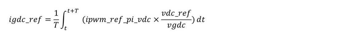 である。
である。
この演算により、蓄電池の充放電電流目標値を、脈流でない一定電流に制御することができる。 (3) In the power conversion system of (2), for example,
T is the period,
igdc_ref is the charge / discharge current target value,
ipwm_ref_pi_vdc is the manipulated variable,
vdc_ref is the voltage target value, and
If vgdc is the detected voltage value,
It is.
By this calculation, the charge / discharge current target value of the storage battery can be controlled to a constant current that is not pulsating.
Tは前記周期、
igdc_refは前記充放電電流目標値、
ipwm_ref_pi_vdcは前記操作量、
vdc_refは前記電圧目標値、及び、
vgdcは前記電圧検出値であるとした場合、
この演算により、蓄電池の充放電電流目標値を、脈流でない一定電流に制御することができる。 (3) In the power conversion system of (2), for example,
T is the period,
igdc_ref is the charge / discharge current target value,
ipwm_ref_pi_vdc is the manipulated variable,
vdc_ref is the voltage target value, and
If vgdc is the detected voltage value,
By this calculation, the charge / discharge current target value of the storage battery can be controlled to a constant current that is not pulsating.
(4)また、(1)の電力変換システムにおいて、前記制御部は、前記第1のDC/DCコンバータの低電圧側の電圧フィードバックに基づく補償量を交流半周期で平均化した値を、前記第1のDC/DCコンバータに含まれる直流リアクトルの電流目標値と定め、前記第1のDC/DCコンバータの低電圧側を一定電圧に制御するようにしてもよい。
この場合、第1のDC/DCコンバータの低電圧側には、平均化処理された平坦な直流電流を流すことができる。そのため、第1のDC/DCコンバータの低電圧側の電圧を一定値とすることができる。 (4) In the power conversion system of (1), the control unit averages a compensation amount based on a voltage feedback on the low voltage side of the first DC / DC converter in an AC half cycle. A current target value of a direct current reactor included in the first DC / DC converter may be determined, and the low voltage side of the first DC / DC converter may be controlled to a constant voltage.
In this case, an averaged flat direct current can be flowed to the low voltage side of the first DC / DC converter. Therefore, the voltage on the low voltage side of the first DC / DC converter can be set to a constant value.
(5)また、(2)又は(3)の電力変換システムにおいて、前記パワーコンディショナは、1又は複数の太陽光発電パネルとも接続される複合型のパワーコンディショナであり、前記第2のDC/DCコンバータは、前記太陽光発電パネルの出力電圧のうち最も高い電圧と一致する電圧を高電圧側に出力するようにしてもよい。
第2のDC/DCコンバータが太陽光発電パネルの出力電圧のうち最も高い電圧と一致する電圧を高電圧側に出力した場合には、パワーコンディショナは、最小スイッチング変換方式の動作を最適化することができる。 (5) Moreover, in the power conversion system of (2) or (3), the power conditioner is a composite power conditioner that is also connected to one or a plurality of photovoltaic power generation panels, and the second DC The / DC converter may output a voltage matching the highest voltage among the output voltages of the photovoltaic power generation panel to the high voltage side.
When the second DC / DC converter outputs a voltage matching the highest voltage among the output voltages of the photovoltaic power generation panel to the high voltage side, the power conditioner optimizes the operation of the minimum switching conversion method. be able to.
(6)同様に、(4)の前記パワーコンディショナは、1又は複数の太陽光発電パネルとも接続される複合型のパワーコンディショナであり、前記第1のDC/DCコンバータは、前記太陽光発電パネルの出力電圧のうち最も高い電圧と一致する電圧を低電圧側に出力するようにしてもよい。
(6) Similarly, the power conditioner of (4) is a composite power conditioner connected to one or a plurality of photovoltaic power generation panels, and the first DC / DC converter includes the sunlight. A voltage that matches the highest voltage among the output voltages of the power generation panel may be output to the low voltage side.
(7)また、(2)、(3)又は(5)の電力変換システムにおいて、前記第2のDC/DCコンバータが自己の高電圧側を一定電圧に制御する場合、前記第2のDC/DCコンバータは、一定にすべき電圧目標値を前記パワーコンディショナから受信する通信を行うようにしてもよい。
この場合、通信により、パワーコンディショナから第2のDC/DCコンバータに対して高電圧側の出力電圧目標値を知らせることができる。例えば、太陽光発電パネルの出力電圧のうち最も高い電圧と一致する電圧をDCバスの電圧とする場合に、出力電圧目標値を第2のDC/DCコンバータに知らせることができる。これにより、第2のDC/DCコンバータは、太陽光発電パネルの出力電圧のうち最も高い電圧と一致する電圧を高電圧側に出力することができる。また、その結果、第1のDC/DCコンバータは、スイッチング停止期間が増加し、このことが、最小スイッチング変換方式の動作の最適化に寄与する。 (7) In the power conversion system according to (2), (3), or (5), when the second DC / DC converter controls its high voltage side to a constant voltage, the second DC / DC The DC converter may perform communication for receiving a voltage target value to be constant from the power conditioner.
In this case, the output voltage target value on the high voltage side can be notified from the power conditioner to the second DC / DC converter by communication. For example, the output voltage target value can be notified to the second DC / DC converter when the voltage matching the highest voltage among the output voltages of the photovoltaic power generation panel is used as the voltage of the DC bus. Thereby, the 2nd DC / DC converter can output the voltage which corresponds with the highest voltage among the output voltages of a photovoltaic power generation panel to the high voltage side. As a result, the first DC / DC converter has an increased switching stop period, which contributes to optimization of the operation of the minimum switching conversion method.
(8)また、(4)又は(6)の電力変換システムにおいて、前記第1のDC/DCコンバータが自己の低電圧側を一定電圧に制御する場合、前記第1のDC/DCコンバータは、前記第2のDC/DCコンバータへ出力電力指令値を送信する通信を行うようにしてもよい。
この場合、第2のDC/DCコンバータに出力電力指令値を知らせることで、第2のDC/DCコンバータは、充放電電流を、出力電力指令値に基づいた定電流に制御することができる。 (8) In the power conversion system according to (4) or (6), when the first DC / DC converter controls its low voltage side to a constant voltage, the first DC / DC converter You may make it perform communication which transmits an output electric power command value to a said 2nd DC / DC converter.
In this case, by notifying the second DC / DC converter of the output power command value, the second DC / DC converter can control the charge / discharge current to a constant current based on the output power command value.
(9)一方、方法の観点からは、直流電源回路とパワーコンディショナとを互いに接続して成り、前記パワーコンディショナは、前記直流電源回路とDCバスとの間に設けられた第1のDC/DCコンバータと、前記DCバスと交流電路との間に設けられたインバータとを有し、前記直流電源回路は、蓄電池と、前記蓄電池と前記第1のDC/DCコンバータとの間に設けられ、直流リアクトルを含む、双方向性の第2のDC/DCコンバータとを有するものである電力変換システムを実行主体とした、その制御方法であって、
前記第2のDC/DCコンバータは、前記蓄電池の電圧を前記第1のDC/DCコンバータの低電圧側の電圧に昇圧し、又は、その逆方向に降圧し、前記第1のDC/DCコンバータと、前記インバータとは、交流半サイクル内で交互に休止期間を有しつつスイッチング動作し、前記第2のDC/DCコンバータの前記直流リアクトルに流れる電流を一定値とする制御を行う、電力変換システムの制御方法である。 (9) On the other hand, from the viewpoint of the method, a DC power supply circuit and a power conditioner are connected to each other, and the power conditioner is a first DC provided between the DC power supply circuit and the DC bus. A DC / DC converter and an inverter provided between the DC bus and the AC circuit, and the DC power supply circuit is provided between the storage battery, the storage battery and the first DC / DC converter. A control method using a power conversion system having a bidirectional DC / DC converter including a direct current reactor as an execution subject,
The second DC / DC converter boosts the voltage of the storage battery to a voltage on the low voltage side of the first DC / DC converter, or steps down the voltage in the opposite direction, so that the first DC / DC converter And the inverter performs a switching operation while alternately having a pause period in an AC half cycle, and performs control to set the current flowing through the DC reactor of the second DC / DC converter to a constant value. This is a system control method.
このような電力変換システムの制御方法によれば、パワーコンディショナと蓄電池との間に入出力電圧の差があっても、第2のDC/DCコンバータが、双方の電圧仲介役をすることができる。従って、出力電圧の異なる各種の蓄電池を第2のDC/DCコンバータ経由でパワーコンディショナに接続することができる。また、第1のDC/DCコンバータとインバータとが交流半サイクル内で交互にスイッチングの休止期間を有する最小スイッチング変換方式では、脈流波形の電流が第1のDC/DCコンバータの低電圧側に流れようとするが、第2のDC/DCコンバータの直流リアクトルに流れる電流を一定値とする制御を、例えば、第1のDC/DCコンバータの低電圧側(第2のDC/DCコンバータの高電圧側)の電圧を一定値とする制御において行うことにより、蓄電池には直流電流のみが流れ、脈流波形の電流は流れない。これにより、蓄電池の内部抵抗による損失を抑制し、蓄電池の劣化を遅らせ、また、蓄電池の性能を充分に発揮させることができる。
According to such a control method of the power conversion system, even if there is a difference in input / output voltage between the power conditioner and the storage battery, the second DC / DC converter can act as a voltage mediator between the two. it can. Therefore, various storage batteries having different output voltages can be connected to the power conditioner via the second DC / DC converter. Further, in the minimum switching conversion method in which the first DC / DC converter and the inverter alternately have a switching pause period in the AC half cycle, the current of the pulsating waveform is on the low voltage side of the first DC / DC converter. Although the control is performed so that the current flowing through the DC reactor of the second DC / DC converter is a constant value, for example, the low voltage side of the first DC / DC converter (the high voltage of the second DC / DC converter is By performing the control in such a manner that the voltage on the voltage side) is a constant value, only a direct current flows through the storage battery, and no current with a pulsating waveform flows. Thereby, the loss by the internal resistance of a storage battery can be suppressed, deterioration of a storage battery can be delayed, and the performance of a storage battery can fully be exhibited.
(10)なお、電力変換システムは、(1)とは別に、以下のように表現することもできる。すなわちこれは、直流電源回路とパワーコンディショナとを互いに接続して成る電力変換システムであって、前記パワーコンディショナは、前記直流電源回路とDCバスとの間に設けられた第1のDC/DCコンバータと、前記DCバスと交流電路との間に設けられ、交流半サイクル内で前記第1のDC/DCコンバータと交互に休止期間を有しつつスイッチング動作するインバータと、を備え、前記直流電源回路は、蓄電池と、前記蓄電池と前記第1のDC/DCコンバータとの間に設けられ、直流リアクトルを含む、双方向性の第2のDC/DCコンバータと、を備え、また、当該電力変換システムは、前記第1のDC/DCコンバータと前記第2のDC/DCコンバータとの間に設けられたコンデンサと、前記第1のDC/DCコンバータに流れる脈動する電流のうちの脈動成分及び直流成分について、前記脈動成分は前記コンデンサが供給し、前記直流成分は前記第2のDC/DCコンバータが供給することで、前記第2のDC/DCコンバータの前記直流リアクトルに流れる電流を一定値とする制御を行う制御部と、を有するものである。
(10) The power conversion system can also be expressed as follows, separately from (1). That is, this is a power conversion system in which a DC power supply circuit and a power conditioner are connected to each other, and the power conditioner is connected to a first DC / DC provided between the DC power supply circuit and a DC bus. A DC converter, and an inverter provided between the DC bus and the AC circuit, and performing switching operation alternately with a pause period in the AC half cycle with the first DC / DC converter. The power supply circuit includes a storage battery, and a bidirectional second DC / DC converter that is provided between the storage battery and the first DC / DC converter and includes a direct current reactor. A conversion system includes a capacitor provided between the first DC / DC converter and the second DC / DC converter, and the first DC / DC converter. As for the pulsating component and the direct current component of the pulsating current flowing through the capacitor, the pulsating component is supplied by the capacitor, and the direct current component is supplied by the second DC / DC converter. And a control unit that controls the current flowing through the DC reactor of the DC converter to have a constant value.
[実施形態の詳細]
以下、実施形態の詳細について図面を参照して説明する。 [Details of the embodiment]
Hereinafter, the details of the embodiment will be described with reference to the drawings.
以下、実施形態の詳細について図面を参照して説明する。 [Details of the embodiment]
Hereinafter, the details of the embodiment will be described with reference to the drawings.
<第1実施形態>
まず、第1実施形態に係る電力変換システム(その制御方法も含む。)について説明する。 <First Embodiment>
First, the power conversion system (including its control method) according to the first embodiment will be described.
まず、第1実施形態に係る電力変換システム(その制御方法も含む。)について説明する。 <First Embodiment>
First, the power conversion system (including its control method) according to the first embodiment will be described.
《回路構成》
図1は、電力変換システム100の概略構成の一例を示す図である。この電力変換システム100は、複数且つ複数種類の直流電源を複合型のパワーコンディショナ1に接続して構成され、商用電力系統3との系統連系が可能である。商用電力系統3とパワーコンディショナ1との間の交流電路5には、需要家の負荷4が接続されている。図において、複合型のパワーコンディショナ1には、例えば3つの太陽光発電パネル7A,7B,7Cが接続されている。なお、この「3つ」というのは一例に過ぎない。また、パワーコンディショナ1には、蓄電池6が、双方向性のDC/DCコンバータ8を介して、接続されている。具体的には、DC/DCコンバータ8の低電圧側(図の左側)が蓄電池6に接続され、高電圧側(図の右側)がパワーコンディショナ1に接続されている。 <Circuit configuration>
FIG. 1 is a diagram illustrating an example of a schematic configuration of apower conversion system 100. The power conversion system 100 is configured by connecting a plurality of types of DC power supplies to the composite power conditioner 1 and can be connected to the commercial power system 3. A consumer's load 4 is connected to an AC power line 5 between the commercial power system 3 and the power conditioner 1. In the figure, for example, three photovoltaic power generation panels 7A, 7B, and 7C are connected to the composite power conditioner 1. The “three” is only an example. In addition, a storage battery 6 is connected to the power conditioner 1 via a bidirectional DC / DC converter 8. Specifically, the low voltage side (left side in the figure) of the DC / DC converter 8 is connected to the storage battery 6, and the high voltage side (right side in the figure) is connected to the power conditioner 1.
図1は、電力変換システム100の概略構成の一例を示す図である。この電力変換システム100は、複数且つ複数種類の直流電源を複合型のパワーコンディショナ1に接続して構成され、商用電力系統3との系統連系が可能である。商用電力系統3とパワーコンディショナ1との間の交流電路5には、需要家の負荷4が接続されている。図において、複合型のパワーコンディショナ1には、例えば3つの太陽光発電パネル7A,7B,7Cが接続されている。なお、この「3つ」というのは一例に過ぎない。また、パワーコンディショナ1には、蓄電池6が、双方向性のDC/DCコンバータ8を介して、接続されている。具体的には、DC/DCコンバータ8の低電圧側(図の左側)が蓄電池6に接続され、高電圧側(図の右側)がパワーコンディショナ1に接続されている。 <Circuit configuration>
FIG. 1 is a diagram illustrating an example of a schematic configuration of a
ここで、例えば数値例を挙げると、商用電力系統3の電圧はAC202V、その場合のピーク値(波高値)は約286V、太陽光発電パネル7A,7B,7Cからパワーコンディショナ1内のDC/DCコンバータ(図示せず。)に入力されMPPT(Maximum Power Point Tracking)制御を経た電圧はDC250Vである。この電圧がパワーコンディショナ1内のDCバス電圧となる。一方、蓄電池6の電圧はDC39~53Vである。従って、蓄電池の6の電圧はDC/DCコンバータ8によって昇圧され、さらに、パワーコンディショナ1内のDC/DCコンバータ11(図2)によってDC250Vまで昇圧される。
Here, to give a numerical example, for example, the voltage of the commercial power system 3 is AC202V, the peak value (peak value) in that case is about 286V, and the DC / DC in the power conditioner 1 from the photovoltaic power generation panels 7A, 7B, 7C The voltage input to a DC converter (not shown) and subjected to MPPT (Maximum Power Point Tracking) control is DC 250V. This voltage becomes the DC bus voltage in the power conditioner 1. On the other hand, the voltage of the storage battery 6 is DC39 to 53V. Therefore, the voltage of the storage battery 6 is boosted by the DC / DC converter 8 and further boosted to DC 250 V by the DC / DC converter 11 (FIG. 2) in the power conditioner 1.
DC/DCコンバータ8を設けることの基本的な効果は、パワーコンディショナ1と蓄電池6との間に入出力電圧の大きな差があっても、昇降圧が可能となり、しかも電圧の適用範囲が広くなることである。従って、出力電圧の異なる各種の蓄電池6を、DC/DCコンバータ8経由で、パワーコンディショナ1に接続することができる。
The basic effect of providing the DC / DC converter 8 is that, even if there is a large difference in input / output voltage between the power conditioner 1 and the storage battery 6, it is possible to increase / decrease the voltage, and the application range of the voltage is wide. It is to become. Therefore, various storage batteries 6 having different output voltages can be connected to the power conditioner 1 via the DC / DC converter 8.
図2は、図1における蓄電池6にのみ注目した電力変換システム100の詳細を示す回路図の一例である。交流電路5と蓄電池6との間には、パワーコンディショナ1と、DC/DCコンバータ8とが設けられている。交流電路5には、図1では省略したが、交流電路5の電力モニタ30が設けられている。
なお、蓄電池6は、実際には単なる電池のみではなく蓄電システムとして構成されており、自己の状態を監視するモニタ機能及び、外部と情報交換するための通信機能を有している(詳細後述)。 FIG. 2 is an example of a circuit diagram showing details of thepower conversion system 100 focusing only on the storage battery 6 in FIG. A power conditioner 1 and a DC / DC converter 8 are provided between the AC circuit 5 and the storage battery 6. Although not shown in FIG. 1, the AC electric circuit 5 is provided with a power monitor 30 for the AC electric circuit 5.
Thestorage battery 6 is actually configured as a power storage system, not just a battery, and has a monitor function for monitoring its own state and a communication function for exchanging information with the outside (details will be described later). .
なお、蓄電池6は、実際には単なる電池のみではなく蓄電システムとして構成されており、自己の状態を監視するモニタ機能及び、外部と情報交換するための通信機能を有している(詳細後述)。 FIG. 2 is an example of a circuit diagram showing details of the
The
パワーコンディショナ1は、主回路要素として、DC/DCコンバータ11と、その高電圧側のDCバス12と、DCバス12に接続されたインバータ13と、DC/DCコンバータ11の低電圧側に接続された低電圧側コンデンサ14と、DCバス12に接続された中間コンデンサ15と、交流リアクトル16と、交流側コンデンサ17とを備えている。DC/DCコンバータ8の高電圧側は、DC/DCコンバータ11の低電圧側と互いに接続されている。インバータ13は、DC/DCコンバータ11の高電圧側と互いに接続されている。
The power conditioner 1 is connected to a DC / DC converter 11, a high voltage side DC bus 12, an inverter 13 connected to the DC bus 12, and a low voltage side of the DC / DC converter 11 as main circuit elements. The low voltage side capacitor 14, the intermediate capacitor 15 connected to the DC bus 12, the AC reactor 16, and the AC side capacitor 17 are provided. The high voltage side of the DC / DC converter 8 is connected to the low voltage side of the DC / DC converter 11. The inverter 13 is connected to the high voltage side of the DC / DC converter 11.
DC/DCコンバータ11は、チョッパ回路を構成する回路要素としての、直流リアクトル11Lと、ハイサイドのスイッチング素子Q3及び逆並列に接続されたダイオードd3と、ローサイドのスイッチング素子Q4及び逆並列に接続されたダイオードd4とを備えている。
インバータ13は、スイッチング素子Q5,Q6,Q7,Q8をフルブリッジ接続したものである。スイッチング素子Q5,Q6,Q7,Q8にはそれぞれ、逆並列にダイオードd5,d6,d7,d8が接続されている。 The DC /DC converter 11 is connected to a DC reactor 11L as circuit elements constituting a chopper circuit, a high-side switching element Q3 and a diode d3 connected in antiparallel, and a low-side switching element Q4 and antiparallel. And a diode d4.
Theinverter 13 is a full-bridge connection of switching elements Q5, Q6, Q7, and Q8. Diodes d5, d6, d7, and d8 are connected in antiparallel to switching elements Q5, Q6, Q7, and Q8, respectively.
インバータ13は、スイッチング素子Q5,Q6,Q7,Q8をフルブリッジ接続したものである。スイッチング素子Q5,Q6,Q7,Q8にはそれぞれ、逆並列にダイオードd5,d6,d7,d8が接続されている。 The DC /
The
DC/DCコンバータ8及びDC/DCコンバータ11は共に、双方向に使用することができ、蓄電池6の放電時は昇圧チョッパとなり、蓄電池6の充電時は降圧チョッパとなる。また、インバータ13は、直流から交流への変換を行うだけでなく双方向性のDC/ACコンバータとなることができ、逆方向の、交流から直流への変換も行うことができる。
Both the DC / DC converter 8 and the DC / DC converter 11 can be used in both directions. When the storage battery 6 is discharged, it becomes a step-up chopper, and when the storage battery 6 is charged, it becomes a step-down chopper. Further, the inverter 13 can not only perform conversion from direct current to alternating current but also be a bidirectional DC / AC converter, and can also perform conversion from alternating current to direct current in the reverse direction.
スイッチング素子Q3~Q8としては、例えば図示しているIGBT(Insulated Gate Bipolar Transistor)や、MOSFET(Metal-Oxide Semiconductor Field-Effect Transistor)を使用することができる。
交流リアクトル16及び交流側コンデンサ17は、フィルタ回路を構成し、インバータ13で発生する高周波成分が交流電路5に漏れ出ることを防止している。 As the switching elements Q3 to Q8, for example, illustrated IGBT (Insulated Gate Bipolar Transistor) or MOSFET (Metal-Oxide Semiconductor Field-Effect Transistor) can be used.
TheAC reactor 16 and the AC side capacitor 17 constitute a filter circuit and prevent high frequency components generated by the inverter 13 from leaking into the AC circuit 5.
交流リアクトル16及び交流側コンデンサ17は、フィルタ回路を構成し、インバータ13で発生する高周波成分が交流電路5に漏れ出ることを防止している。 As the switching elements Q3 to Q8, for example, illustrated IGBT (Insulated Gate Bipolar Transistor) or MOSFET (Metal-Oxide Semiconductor Field-Effect Transistor) can be used.
The
計測用の回路要素としては、低電圧側コンデンサ14の両端電圧を検出する電圧センサ18と、直流リアクトル11Lに流れる電流を検出する電流センサ19と、DCバス12の電圧すなわち中間コンデンサ15の両端電圧を検出する電圧センサ20と、交流リアクトル16に流れる電流を検出する電流センサ21と、交流側コンデンサ17の両端電圧を検出する電圧センサ22とが設けられている。各センサの検出出力信号は、制御部10に送られる。
As circuit elements for measurement, a voltage sensor 18 for detecting the voltage across the low-voltage side capacitor 14, a current sensor 19 for detecting the current flowing through the DC reactor 11 </ b> L, and the voltage of the DC bus 12, that is, the voltage across the intermediate capacitor 15. Are provided, a current sensor 21 for detecting the current flowing through the AC reactor 16, and a voltage sensor 22 for detecting the voltage across the AC capacitor 17. The detection output signal of each sensor is sent to the control unit 10.
制御部10は、スイッチング素子Q3,Q4,Q5~Q8のオン・オフを制御する。
制御部10は例えば、コンピュータを含み、ソフトウェア(コンピュータプログラム)をコンピュータが実行することで、必要な制御機能を実現する。ソフトウェアは、制御部の記憶装置(図示せず。)に格納される。但し、コンピュータを含まないハードウェアのみの回路で制御部10を構成することも可能ではある。Control unit 10 controls on / off of switching elements Q3, Q4, Q5 to Q8.
Thecontrol unit 10 includes, for example, a computer, and a necessary control function is realized by the software (computer program) being executed by the computer. The software is stored in a storage device (not shown) of the control unit. However, it is also possible to configure the control unit 10 with a hardware-only circuit that does not include a computer.
制御部10は例えば、コンピュータを含み、ソフトウェア(コンピュータプログラム)をコンピュータが実行することで、必要な制御機能を実現する。ソフトウェアは、制御部の記憶装置(図示せず。)に格納される。但し、コンピュータを含まないハードウェアのみの回路で制御部10を構成することも可能ではある。
The
一方、DC/DCコンバータ8は、チョッパ回路としての、直流リアクトル8Lと、ハイサイドのスイッチング素子Q1及び逆並列に接続されたダイオードd1と、ローサイドのスイッチング素子Q2及び逆並列に接続されたダイオードd2とを備えている。また、DC/DCコンバータ8の低電圧側には低電圧側コンデンサ81が接続され、高電圧側には高電圧側コンデンサ82が接続されている。スイッチング素子Q1,Q2としては例えばIGBTやMOSFETを用いることができる。
On the other hand, the DC / DC converter 8 includes a DC reactor 8L as a chopper circuit, a high-side switching element Q1 and a diode d1 connected in reverse parallel, a low-side switching element Q2 and a diode d2 connected in reverse parallel. And. A low voltage side capacitor 81 is connected to the low voltage side of the DC / DC converter 8, and a high voltage side capacitor 82 is connected to the high voltage side. As the switching elements Q1, Q2, for example, an IGBT or a MOSFET can be used.
計測用の回路要素としては、コンデンサ81の両端電圧を検出する電圧センサ83と、直流リアクトル8Lに流れる電流を検出する電流センサ84と、高電圧側コンデンサ82の両端電圧を検出する電圧センサ85とが設けられている。各センサの検出出力信号は、制御部80に送られる。
As circuit elements for measurement, there are a voltage sensor 83 for detecting the voltage across the capacitor 81, a current sensor 84 for detecting the current flowing through the DC reactor 8L, and a voltage sensor 85 for detecting the voltage across the high-voltage side capacitor 82. Is provided. The detection output signal of each sensor is sent to the control unit 80.
制御部80は、スイッチング素子Q1,Q2のオン・オフを制御する。
制御部80は例えば、コンピュータを含み、ソフトウェア(コンピュータプログラム)をコンピュータが実行することで、必要な制御機能を実現する。ソフトウェアは、制御部の記憶装置(図示せず。)に格納される。但し、コンピュータを含まないハードウェアのみの回路で制御部80を構成することも可能ではある。Control unit 80 controls on / off of switching elements Q1, Q2.
Thecontrol unit 80 includes, for example, a computer, and realizes necessary control functions by causing the computer to execute software (computer program). The software is stored in a storage device (not shown) of the control unit. However, it is also possible to configure the control unit 80 with a hardware-only circuit that does not include a computer.
制御部80は例えば、コンピュータを含み、ソフトウェア(コンピュータプログラム)をコンピュータが実行することで、必要な制御機能を実現する。ソフトウェアは、制御部の記憶装置(図示せず。)に格納される。但し、コンピュータを含まないハードウェアのみの回路で制御部80を構成することも可能ではある。
The
DC/DCコンバータ8及び蓄電池6は、直流電源回路9を構成している。すなわち、電力変換システム100は、直流電源回路9とパワーコンディショナ1とを互いに接続して成るものである。そして、パワーコンディショナ1は、直流電源回路9とDCバス12との間に設けられた第1のDC/DCコンバータ11と、DCバス12と交流電路5との間に設けられ、交流半サイクル内で第1のDC/DCコンバータ11と交互に休止期間を有しつつスイッチング動作するインバータ13とを備えている。
また、直流電源回路9の第2のDC/DCコンバータ8は、蓄電池6と第1のDC/DCコンバータ11との間に設けられており、直流リアクトル8Lを含む、双方向性のコンバータである。 The DC /DC converter 8 and the storage battery 6 constitute a DC power supply circuit 9. That is, the power conversion system 100 is configured by connecting the DC power supply circuit 9 and the power conditioner 1 to each other. The power conditioner 1 is provided between the first DC / DC converter 11 provided between the DC power supply circuit 9 and the DC bus 12, the DC bus 12 and the AC circuit 5, and is connected to the AC half cycle. The first DC / DC converter 11 and the inverter 13 that performs a switching operation alternately with a pause period are provided.
The second DC /DC converter 8 of the DC power supply circuit 9 is a bidirectional converter that is provided between the storage battery 6 and the first DC / DC converter 11 and includes a DC reactor 8L. .
また、直流電源回路9の第2のDC/DCコンバータ8は、蓄電池6と第1のDC/DCコンバータ11との間に設けられており、直流リアクトル8Lを含む、双方向性のコンバータである。 The DC /
The second DC /
また、制御部10及び制御部80は、通信機能を有しており、制御部10は、電力モニタ30及び制御部80と、必要な通信を行うことができる。制御部80は、蓄電池6及び制御部10と、必要な通信を行うことができる。
Further, the control unit 10 and the control unit 80 have a communication function, and the control unit 10 can perform necessary communication with the power monitor 30 and the control unit 80. The control unit 80 can perform necessary communication with the storage battery 6 and the control unit 10.
《最小スイッチング変換方式の説明》
図3及び図4は、最小スイッチング変換方式における、DC/DCコンバータ11及びインバータ13の動作の特徴を簡略に示す波形図である。両図は同じ内容を示しているが、図3は特に、直流入力から交流出力までの振幅の関係が見やすいように横書き表示し、図4は特に、制御のタイミングが見やすいように縦書き表示している。図3の上段及び図4の左欄はそれぞれ、比較のために、最小スイッチング変換方式ではない伝統的なスイッチング制御を表す波形図である。また、図3の下段及び図4の右欄はそれぞれ、最小スイッチング変換方式の動作を示す波形図である。 <Description of minimum switching conversion method>
FIG. 3 and FIG. 4 are waveform diagrams simply showing the characteristics of the operation of the DC /DC converter 11 and the inverter 13 in the minimum switching conversion method. Although both figures show the same contents, FIG. 3 is displayed horizontally so that the amplitude relationship from DC input to AC output is easy to see, and FIG. 4 is particularly displayed vertically so that the timing of control is easy to see. ing. The upper part of FIG. 3 and the left column of FIG. 4 are waveform diagrams representing traditional switching control that is not the minimum switching conversion method, for comparison. Further, the lower part of FIG. 3 and the right column of FIG. 4 are waveform diagrams showing the operation of the minimum switching conversion method.
図3及び図4は、最小スイッチング変換方式における、DC/DCコンバータ11及びインバータ13の動作の特徴を簡略に示す波形図である。両図は同じ内容を示しているが、図3は特に、直流入力から交流出力までの振幅の関係が見やすいように横書き表示し、図4は特に、制御のタイミングが見やすいように縦書き表示している。図3の上段及び図4の左欄はそれぞれ、比較のために、最小スイッチング変換方式ではない伝統的なスイッチング制御を表す波形図である。また、図3の下段及び図4の右欄はそれぞれ、最小スイッチング変換方式の動作を示す波形図である。 <Description of minimum switching conversion method>
FIG. 3 and FIG. 4 are waveform diagrams simply showing the characteristics of the operation of the DC /
まず、図3の上段(又は図4の左欄)において、伝統的なスイッチング制御では、入力される直流電圧Vdcに対するDC/DCコンバータの出力は、Vdcよりも高い値の等間隔のパルス列状である。この出力は中間コンデンサによって平滑化され、DCバスに、電圧VOとして現れる。これに対してインバータは、PWM(Pulse Width Modulation)制御されたスイッチングを半周期で極性反転しながら行う。この結果、最終的な平滑化を経て、正弦波の交流電圧Vacが得られる。
First, in the upper part of FIG. 3 (or the left column of FIG. 4), in the traditional switching control, the output of the DC / DC converter with respect to the input DC voltage V dc is a pulse train of equal intervals higher than V dc. Is. This output is smoothed by the intermediate capacitor, the DC bus, appears as voltage V O. In contrast, the inverter performs PWM (Pulse Width Modulation) controlled switching while inverting the polarity in a half cycle. As a result, a sinusoidal AC voltage V ac is obtained through final smoothing.
次に、図3の下段の最小スイッチング変換方式では、交流波形の電圧目標値Vacの瞬時値の絶対値と、入力である直流電圧Vdcとの比較結果に応じて、DC/DCコンバータ11とインバータ13とが動作する。すなわち、電圧目標値Vacの絶対値においてVac<Vdc(又はVac≦Vdc)のときは、DC/DCコンバータ11は停止し(図中の「ST」)、Vac≧Vdc(又はVac>Vdc)のときは、DC/DCコンバータ11が昇圧動作を行う(図中の「OP」)。DC/DCコンバータ11の出力は中間コンデンサ15により平滑化され、DCバス12に、図示の電圧VOとして現れる。
Next, in the minimum switching conversion method in the lower stage of FIG. 3, the DC / DC converter 11 corresponds to the comparison result between the absolute value of the instantaneous value of the voltage target value V ac of the AC waveform and the input DC voltage V dc. And the inverter 13 operate. That is, when V ac <V dc (or V ac ≦ V dc ) in the absolute value of the voltage target value V ac , the DC / DC converter 11 stops (“ST” in the figure), and V ac ≧ V dc When (or V ac > V dc ), the DC / DC converter 11 performs a boosting operation (“OP” in the figure). The output of the DC / DC converter 11 is smoothed by the intermediate capacitor 15, the DC bus 12, it appears as voltage V O shown.
ここで、中間コンデンサ15が小容量(例えばマイクロファラッドのレベル)である。そのため、交流波形の絶対値のピーク前後となる一部の波形が平滑化されずにそのまま残る。すなわち、平滑は、DC/DCコンバータ11による高周波のスイッチングの痕跡を消す程度には作用するが、商用周波数の2倍程度の低周波を平滑化することはできないように中間コンデンサ15が小容量になっている。
Here, the intermediate capacitor 15 has a small capacity (for example, a microfarad level). Therefore, a part of the waveform around the peak of the absolute value of the AC waveform remains without being smoothed. That is, the smoothing works to the extent that the trace of the high frequency switching by the DC / DC converter 11 is erased, but the intermediate capacitor 15 has a small capacity so that the low frequency about twice the commercial frequency cannot be smoothed. It has become.
これに対してインバータ13は、電圧目標値Vacの絶対値と、直流電圧Vdcとの比較結果に応じて、Vac<Vdc(又はVac≦Vdc)のときは、高周波スイッチングを行い(図中の「OP」)、Vac≧Vdc(又はVac>Vdc)のときは、高周波スイッチングを停止する(図中の「ST」)。高周波スイッチングを停止しているときのインバータ13は、スイッチング素子Q5,Q8がオン、Q6,Q7がオフの状態と、スイッチング素子Q5,Q8がオフ、Q6,Q7がオンの状態のいずれかを選択することにより、必要な極性反転のみを行う。インバータ13の出力は交流リアクトル16及び交流側コンデンサ17により平滑化され、所望の交流出力が得られる。
On the other hand, the inverter 13 performs high-frequency switching when V ac <V dc (or V ac ≦ V dc ) according to the comparison result between the absolute value of the voltage target value V ac and the DC voltage V dc. If it is performed (“OP” in the figure) and V ac ≧ V dc (or V ac > V dc ), high-frequency switching is stopped (“ST” in the figure). When the high frequency switching is stopped, the inverter 13 selects one of the switching elements Q5 and Q8 being on, Q6 and Q7 being off, and the switching elements Q5 and Q8 being off and Q6 and Q7 being on. By doing so, only necessary polarity inversion is performed. The output of the inverter 13 is smoothed by the AC reactor 16 and the AC side capacitor 17, and a desired AC output is obtained.
ここで、図4の右欄に示すように、DC/DCコンバータ11とインバータ13とは、交互に高周波スイッチングの動作をしており、DC/DCコンバータ11が昇圧の動作をしているときは、インバータ13は高周波スイッチングを停止し、DCバス12の電圧に対して必要な極性反転のみを行っている。逆に、インバータ13が高周波スイッチング動作するときは、DC/DCコンバータ11は停止して、低電圧側コンデンサ14の両端電圧が、直流リアクトル11L及びダイオードd3を介してDCバス12に現れる。
Here, as shown in the right column of FIG. 4, the DC / DC converter 11 and the inverter 13 are alternately performing high-frequency switching operations, and when the DC / DC converter 11 is performing a boosting operation. The inverter 13 stops high-frequency switching and performs only necessary polarity inversion with respect to the voltage of the DC bus 12. Conversely, when the inverter 13 performs high-frequency switching operation, the DC / DC converter 11 stops and the voltage across the low-voltage side capacitor 14 appears on the DC bus 12 via the DC reactor 11L and the diode d3.
以上のようにして、DC/DCコンバータ11とインバータ13とによる最小スイッチング変換方式の動作が行われる。
As described above, the operation of the minimum switching conversion method by the DC / DC converter 11 and the inverter 13 is performed.
《第2のDC/DCコンバータの制御》
次に、第2の(外付けの)DC/DCコンバータ8の制御について説明する。
図5は、DC/DCコンバータ8の高電圧側の電圧制御ブロック線図である。制御の実行主体は制御部80である。図において、制御部80は、電圧センサ85(図2)が検出する高電圧側の電圧検出値vdcを制御量として、高電圧側の電圧目標値vdc_refと、制御量vdcとの誤差量dvdcを計算する。そして、制御部80は、誤差量dvdcをPI補償器に通して、操作量ipwm_ref_pi_vdcを算出する。 << Control of Second DC / DC Converter >>
Next, control of the second (external) DC /DC converter 8 will be described.
FIG. 5 is a voltage control block diagram on the high voltage side of the DC /DC converter 8. The control execution subject is the control unit 80. In the figure, the control unit 80 uses a voltage detection value vdc on the high voltage side detected by the voltage sensor 85 (FIG. 2) as a control amount, and calculates an error amount dvdc between the voltage target value vdc_ref on the high voltage side and the control amount vdc. calculate. Then, the control unit 80 passes the error amount dvdc through the PI compensator and calculates the operation amount ipwm_ref_pi_vdc.
次に、第2の(外付けの)DC/DCコンバータ8の制御について説明する。
図5は、DC/DCコンバータ8の高電圧側の電圧制御ブロック線図である。制御の実行主体は制御部80である。図において、制御部80は、電圧センサ85(図2)が検出する高電圧側の電圧検出値vdcを制御量として、高電圧側の電圧目標値vdc_refと、制御量vdcとの誤差量dvdcを計算する。そして、制御部80は、誤差量dvdcをPI補償器に通して、操作量ipwm_ref_pi_vdcを算出する。 << Control of Second DC / DC Converter >>
Next, control of the second (external) DC /
FIG. 5 is a voltage control block diagram on the high voltage side of the DC /
以下に、直流リアクトル8Lの電流目標値igdc_refを求める式を示す。
なお、文字フォントの違い(立体/イタリック体)には意味は無く、同じ文字は同じ量を表している(以下同様)。 Below, the formula which calculates | requires the electric current target value igdc_ref of theDC reactor 8L is shown.
Note that the difference between character fonts (solid / italic) has no meaning, and the same character represents the same amount (the same applies hereinafter).
なお、文字フォントの違い(立体/イタリック体)には意味は無く、同じ文字は同じ量を表している(以下同様)。 Below, the formula which calculates | requires the electric current target value igdc_ref of the
Note that the difference between character fonts (solid / italic) has no meaning, and the same character represents the same amount (the same applies hereinafter).

上記の式において、高電圧側の電圧制御ブロック線図で算出した操作量ipwm_ref_pi_vdcは、物理的にはDC/DCコンバータ8の高電圧側コンデンサ82に入出する電流を意味している。従って、DC/DCコンバータ8における直流リアクトル8Lの電流目標値の算出にあたっては、高電圧側の電圧目標値vdc_refを、電圧センサ83(図2)が検出する蓄電池側の電圧検出値vgdcで除した値を、操作量ipwm_ref_pi_vdcに乗算して、直流リアクトル8Lの電流目標値に換算する。そして、その換算値をPWM周期よりも長い一定の周期Tで平均化して直流リアクトル8Lの電流目標値igdc_refとする。交流成分を取り除くことが目的であるためTは交流周期(例えば1/60[秒])、またはその1/2とする。
In the above equation, the manipulated variable ipwm_ref_pi_vdc calculated in the voltage control block diagram on the high voltage side physically means the current input / output to / from the high voltage side capacitor 82 of the DC / DC converter 8. Therefore, in calculating the current target value of the DC reactor 8L in the DC / DC converter 8, the voltage target value vdc_ref on the high voltage side is divided by the voltage detection value vgdc on the storage battery side detected by the voltage sensor 83 (FIG. 2). The value is multiplied by the manipulated variable ipwm_ref_pi_vdc to convert it into a current target value of the DC reactor 8L. Then, the converted value is averaged at a constant period T longer than the PWM period to obtain the current target value igdc_ref of the DC reactor 8L. Since the purpose is to remove the AC component, T is set to an AC cycle (for example, 1/60 [seconds]) or 1/2 thereof.
図6は、DC/DCコンバータ8における直流リアクトル8Lの電流制御ブロック線図である。制御部80は、電流センサ84が検出する直流リアクトル8Lの電流検出値igdcを制御量として、直流リアクトル8Lの電流目標値igdc_refとの誤差量digdcを計算する。そして、制御部80は、誤差量digdcをPI補償器に通し、その計算結果に外乱補償として蓄電池側の電圧検出値vgdcを加算して、さらに高電圧側の電圧検出値vdcで除算する。これにより、操作量th_swが算出される。この操作量を用いてDC/DCコンバータ8のスイッチング素子Q1,Q2のデューティを決定する。
FIG. 6 is a current control block diagram of the DC reactor 8L in the DC / DC converter 8. The control unit 80 calculates an error amount digdc from the target current value igdc_ref of the DC reactor 8L using the current detection value igdc of the DC reactor 8L detected by the current sensor 84 as a control amount. Then, the control unit 80 passes the error amount digdc through the PI compensator, adds the voltage detection value vgdc on the storage battery side as disturbance compensation to the calculation result, and further divides by the voltage detection value vdc on the high voltage side. Thereby, the operation amount th_sw is calculated. The duty of the switching elements Q1, Q2 of the DC / DC converter 8 is determined using this manipulated variable.
なお、DC/DCコンバータ8は、太陽光発電パネル7A,7B,7Cの出力電圧のうち最も高い電圧と一致する電圧を高電圧側に出力する。
DC/DCコンバータ8が、太陽光発電パネル7A,7B,7Cの出力電圧のうち最も高い電圧と一致する電圧を高電圧側に出力した場合には、DC/DCコンバータ11のスイッチング停止期間が増加する。このことは、パワーコンディショナ1における最小スイッチング変換方式の動作の最適化に寄与する。
なお、同様に、DC/DCコンバータ11が、太陽光発電パネル7A,7B,7Cの出力電圧のうち最も高い電圧と一致する電圧を低電圧側に出力することもできる。 The DC /DC converter 8 outputs to the high voltage side a voltage that matches the highest voltage among the output voltages of the photovoltaic power generation panels 7A, 7B, and 7C.
When the DC /DC converter 8 outputs a voltage that matches the highest voltage among the output voltages of the photovoltaic power generation panels 7A, 7B, and 7C to the high voltage side, the switching stop period of the DC / DC converter 11 increases. To do. This contributes to optimization of the operation of the minimum switching conversion method in the power conditioner 1.
Similarly, the DC /DC converter 11 can output a voltage matching the highest voltage among the output voltages of the photovoltaic power generation panels 7A, 7B, and 7C to the low voltage side.
DC/DCコンバータ8が、太陽光発電パネル7A,7B,7Cの出力電圧のうち最も高い電圧と一致する電圧を高電圧側に出力した場合には、DC/DCコンバータ11のスイッチング停止期間が増加する。このことは、パワーコンディショナ1における最小スイッチング変換方式の動作の最適化に寄与する。
なお、同様に、DC/DCコンバータ11が、太陽光発電パネル7A,7B,7Cの出力電圧のうち最も高い電圧と一致する電圧を低電圧側に出力することもできる。 The DC /
When the DC /
Similarly, the DC /
《検証》
上記のDC/DCコンバータ8の制御の結果を検証する。これは、一例として、約1.5kWの電力を、商用電力系統3から蓄電池6に充電する場合である。
図7は、比較のために、図2からDC/DCコンバータ8を削除した回路図である。図8は、図7の回路における電流センサ21によって検出される系統電流(周波数は50Hz)の波形図である。また、図9は、図7の回路における電圧センサ22によって検出される系統電圧(周波数は50Hz)の波形図である。そして、図10は、図7の回路における電流センサ19によって検出される蓄電池6への充電電流の波形図である。前述の最小スイッチング変換方式により、充電電流は脈流となっており、平均値として29.6[A]、0から見たピーク値は68[A]、脈流の周期は交流の周期の1/2である。 <Verification>
The control result of the DC /DC converter 8 is verified. As an example, this is a case where about 1.5 kW of power is charged from the commercial power system 3 to the storage battery 6.
FIG. 7 is a circuit diagram in which the DC /DC converter 8 is omitted from FIG. 2 for comparison. FIG. 8 is a waveform diagram of the system current (frequency is 50 Hz) detected by the current sensor 21 in the circuit of FIG. FIG. 9 is a waveform diagram of the system voltage (frequency is 50 Hz) detected by the voltage sensor 22 in the circuit of FIG. FIG. 10 is a waveform diagram of the charging current to the storage battery 6 detected by the current sensor 19 in the circuit of FIG. According to the above-described minimum switching conversion method, the charging current is pulsating, the average value is 29.6 [A], the peak value viewed from 0 is 68 [A], and the pulsating cycle is 1 of the alternating cycle. / 2.
上記のDC/DCコンバータ8の制御の結果を検証する。これは、一例として、約1.5kWの電力を、商用電力系統3から蓄電池6に充電する場合である。
図7は、比較のために、図2からDC/DCコンバータ8を削除した回路図である。図8は、図7の回路における電流センサ21によって検出される系統電流(周波数は50Hz)の波形図である。また、図9は、図7の回路における電圧センサ22によって検出される系統電圧(周波数は50Hz)の波形図である。そして、図10は、図7の回路における電流センサ19によって検出される蓄電池6への充電電流の波形図である。前述の最小スイッチング変換方式により、充電電流は脈流となっており、平均値として29.6[A]、0から見たピーク値は68[A]、脈流の周期は交流の周期の1/2である。 <Verification>
The control result of the DC /
FIG. 7 is a circuit diagram in which the DC /
次に、図2の回路に示す電力変換システム100についての波形図を示す。
電流センサ21によって検出される系統電流(周波数は50Hz)の波形図、及び、電圧センサ22によって検出される系統電圧(周波数は50Hz)の波形図は、それぞれ、図8及び図9と同じである。 Next, a waveform diagram of thepower conversion system 100 shown in the circuit of FIG. 2 is shown.
The waveform diagram of the system current (frequency is 50 Hz) detected by thecurrent sensor 21 and the waveform diagram of the system voltage (frequency is 50 Hz) detected by the voltage sensor 22 are the same as those in FIGS. 8 and 9, respectively. .
電流センサ21によって検出される系統電流(周波数は50Hz)の波形図、及び、電圧センサ22によって検出される系統電圧(周波数は50Hz)の波形図は、それぞれ、図8及び図9と同じである。 Next, a waveform diagram of the
The waveform diagram of the system current (frequency is 50 Hz) detected by the
図11は、電圧センサ18,85によって検出されるDC/DCコンバータ8と、パワーコンディショナ1との相互接続点での電圧の波形図である。この波形図は、縦軸方向にスケールを拡大している。平均値は200[V]、ピーク・トゥー・ピークの値は、6[V]である。
そして、図12は、図2の回路における電流センサ84によって検出される蓄電池6への充電電流の波形図である。図示のように、極めて微小な変動はあるものの、充電電流は直流と言える状態となっていることがわかる。電流の平均値は、30.2[A]、ピーク・トゥー・ピークの値は、1.8[A]である。 FIG. 11 is a waveform diagram of a voltage at an interconnection point between the DC /DC converter 8 detected by the voltage sensors 18 and 85 and the power conditioner 1. In this waveform diagram, the scale is enlarged in the vertical axis direction. The average value is 200 [V], and the peak-to-peak value is 6 [V].
FIG. 12 is a waveform diagram of the charging current to thestorage battery 6 detected by the current sensor 84 in the circuit of FIG. As shown in the figure, it can be seen that the charging current is in a state that can be said to be a direct current, although there are extremely small fluctuations. The average value of the current is 30.2 [A], and the peak-to-peak value is 1.8 [A].
そして、図12は、図2の回路における電流センサ84によって検出される蓄電池6への充電電流の波形図である。図示のように、極めて微小な変動はあるものの、充電電流は直流と言える状態となっていることがわかる。電流の平均値は、30.2[A]、ピーク・トゥー・ピークの値は、1.8[A]である。 FIG. 11 is a waveform diagram of a voltage at an interconnection point between the DC /
FIG. 12 is a waveform diagram of the charging current to the
以上の検証結果より、DC/DCコンバータ8を蓄電池6とパワーコンディショナ1との間に設け、所定の制御を行うことで、蓄電池6への充電電流が直流になることが示された。なお、ここでは充電について記載したが、蓄電池6の放電時にも同様に、放電電流は直流となる。
充放電電流が直流になると、平均値が同じ値である脈流で充放電する場合と比べて、蓄電池6の内部抵抗による損失は2/3に低下する。 From the above verification results, it was shown that the charging current to thestorage battery 6 becomes DC by providing the DC / DC converter 8 between the storage battery 6 and the power conditioner 1 and performing predetermined control. Although charging is described here, the discharge current is also a direct current when the storage battery 6 is discharged.
When the charging / discharging current becomes a direct current, the loss due to the internal resistance of thestorage battery 6 is reduced to 2/3 as compared with the case where charging / discharging is performed with the pulsating current having the same average value.
充放電電流が直流になると、平均値が同じ値である脈流で充放電する場合と比べて、蓄電池6の内部抵抗による損失は2/3に低下する。 From the above verification results, it was shown that the charging current to the
When the charging / discharging current becomes a direct current, the loss due to the internal resistance of the
《通信について》
DC/DCコンバータ8を蓄電池6とパワーコンディショナ1との間に置くことによって、DC/DCコンバータ8の制御部80に通信の仲介役をさせることができる。例えば、DC/DCコンバータ8に、蓄電池6との通信に関して、各種の通信インターフェース機能を搭載すれば、例えば蓄電池メーカーによって各種の通信仕様となっている蓄電池6を使用しても、DC/DCコンバータ8との通信を行うことができる。パワーコンディショナ1から見れば、DC/DCコンバータ8とさえ通信できれば、蓄電池6の通信仕様は問わないで済むことになり、実用上、至便である。 《About communication》
By placing the DC /DC converter 8 between the storage battery 6 and the power conditioner 1, the control unit 80 of the DC / DC converter 8 can act as an intermediary for communication. For example, if various communication interface functions are installed in the DC / DC converter 8 for communication with the storage battery 6, even if the storage battery 6 having various communication specifications by the storage battery manufacturer is used, for example, the DC / DC converter 8 can be communicated. From the viewpoint of the power conditioner 1, as long as communication with the DC / DC converter 8 is possible, the communication specification of the storage battery 6 is not limited, which is practically convenient.
DC/DCコンバータ8を蓄電池6とパワーコンディショナ1との間に置くことによって、DC/DCコンバータ8の制御部80に通信の仲介役をさせることができる。例えば、DC/DCコンバータ8に、蓄電池6との通信に関して、各種の通信インターフェース機能を搭載すれば、例えば蓄電池メーカーによって各種の通信仕様となっている蓄電池6を使用しても、DC/DCコンバータ8との通信を行うことができる。パワーコンディショナ1から見れば、DC/DCコンバータ8とさえ通信できれば、蓄電池6の通信仕様は問わないで済むことになり、実用上、至便である。 《About communication》
By placing the DC /
図13は、情報信号の送受信の例を示す図である。DC/DCコンバータ8と蓄電池6との間では、信号S1,S2が送受信される。パワーコンディショナ1とDC/DCコンバータ8との間では、信号S3,S4が送受信される。電力モニタ30とパワーコンディショナ1との間では、信号S5,S6が送受信される。
FIG. 13 is a diagram showing an example of information signal transmission / reception. Signals S 1 and S 2 are transmitted and received between the DC / DC converter 8 and the storage battery 6. Signals S3 and S4 are transmitted and received between the power conditioner 1 and the DC / DC converter 8. Signals S5 and S6 are transmitted and received between the power monitor 30 and the power conditioner 1.
信号の内容としては、例えば以下のものがある。PCSはパワーコンディショナ、PVは太陽光発電パネル、DC/DCはDC/DCコンバータ8を、それぞれ意味する略語である。
S1:運転開始指示、運転停止指示
S2:蓄電池両端電圧、セル電圧、システム動作情報、電流、SOC(State of Charge)
S3:DC/DC動作指示、PCS動作状況
S4:DC/DC動作モード、PCSへの要求状態、蓄電池動作情報
S5:PCS動作指示、蓄電池動作指示、蓄電池充放電目標値、PCS出力電力最大値、エラー解除フラグ
S6:PCS動作内容、蓄電池動作内容、PCS出力電力、各PV発電電力、蓄電池充放電電力、蓄電池容量(SOC)、PCS状態、蓄電池状態、ログコード Examples of the signal contents include the following. PCS is an abbreviation that means a power conditioner, PV is a solar power generation panel, and DC / DC is a DC /DC converter 8.
S1: Operation start instruction, operation stop instruction S2: Storage battery voltage, cell voltage, system operation information, current, SOC (State of Charge)
S3: DC / DC operation instruction, PCS operation status S4: DC / DC operation mode, request state to PCS, storage battery operation information S5: PCS operation instruction, storage battery operation instruction, storage battery charge / discharge target value, PCS output power maximum value, Error release flag S6: PCS operation content, storage battery operation content, PCS output power, each PV generated power, storage battery charge / discharge power, storage battery capacity (SOC), PCS state, storage battery state, log code
S1:運転開始指示、運転停止指示
S2:蓄電池両端電圧、セル電圧、システム動作情報、電流、SOC(State of Charge)
S3:DC/DC動作指示、PCS動作状況
S4:DC/DC動作モード、PCSへの要求状態、蓄電池動作情報
S5:PCS動作指示、蓄電池動作指示、蓄電池充放電目標値、PCS出力電力最大値、エラー解除フラグ
S6:PCS動作内容、蓄電池動作内容、PCS出力電力、各PV発電電力、蓄電池充放電電力、蓄電池容量(SOC)、PCS状態、蓄電池状態、ログコード Examples of the signal contents include the following. PCS is an abbreviation that means a power conditioner, PV is a solar power generation panel, and DC / DC is a DC /
S1: Operation start instruction, operation stop instruction S2: Storage battery voltage, cell voltage, system operation information, current, SOC (State of Charge)
S3: DC / DC operation instruction, PCS operation status S4: DC / DC operation mode, request state to PCS, storage battery operation information S5: PCS operation instruction, storage battery operation instruction, storage battery charge / discharge target value, PCS output power maximum value, Error release flag S6: PCS operation content, storage battery operation content, PCS output power, each PV generated power, storage battery charge / discharge power, storage battery capacity (SOC), PCS state, storage battery state, log code
《第1実施形態のまとめ》
上記電力変換システム100では、パワーコンディショナ1と蓄電池6との間に入出力電圧の大きな差があっても、昇降圧が可能となり、しかも電圧の適用範囲が広くなる。従って、出力電圧の異なる各種の蓄電池をパワーコンディショナ1に接続することができる。また、第1のDC/DCコンバータ11とインバータ13とが交流半サイクル内で交互にスイッチングの休止期間を有する最小スイッチング変換方式では、脈流波形の電流が第1のDC/DCコンバータ11の低電圧側に流れようとするが、第2のDC/DCコンバータ8の直流リアクトル8Lに流れる電流を一定値とする制御(言い換えれば、DC/DCコンバータ8の高電圧側の電圧を一定値とする制御)を行うことにより、蓄電池6には直流電流のみが流れ、脈流波形の電流は流れない。これにより、蓄電池6の内部抵抗による損失を抑制し、蓄電池6の劣化を遅らせ、また、蓄電池6の性能を充分に発揮させることができる。 << Summary of First Embodiment >>
In thepower conversion system 100, even if there is a large difference in input / output voltage between the power conditioner 1 and the storage battery 6, the voltage can be stepped up and down, and the applicable range of voltage is widened. Therefore, various storage batteries having different output voltages can be connected to the power conditioner 1. Further, in the minimum switching conversion method in which the first DC / DC converter 11 and the inverter 13 alternately have a switching pause period in an AC half cycle, the current of the pulsating waveform is lower than that of the first DC / DC converter 11. Although control is performed to flow to the voltage side, the current flowing through the DC reactor 8L of the second DC / DC converter 8 is set to a constant value (in other words, the voltage on the high voltage side of the DC / DC converter 8 is set to a constant value). Control), only the direct current flows through the storage battery 6 and the current of the pulsating waveform does not flow. Thereby, the loss by the internal resistance of the storage battery 6 can be suppressed, the deterioration of the storage battery 6 can be delayed, and the performance of the storage battery 6 can be exhibited sufficiently.
上記電力変換システム100では、パワーコンディショナ1と蓄電池6との間に入出力電圧の大きな差があっても、昇降圧が可能となり、しかも電圧の適用範囲が広くなる。従って、出力電圧の異なる各種の蓄電池をパワーコンディショナ1に接続することができる。また、第1のDC/DCコンバータ11とインバータ13とが交流半サイクル内で交互にスイッチングの休止期間を有する最小スイッチング変換方式では、脈流波形の電流が第1のDC/DCコンバータ11の低電圧側に流れようとするが、第2のDC/DCコンバータ8の直流リアクトル8Lに流れる電流を一定値とする制御(言い換えれば、DC/DCコンバータ8の高電圧側の電圧を一定値とする制御)を行うことにより、蓄電池6には直流電流のみが流れ、脈流波形の電流は流れない。これにより、蓄電池6の内部抵抗による損失を抑制し、蓄電池6の劣化を遅らせ、また、蓄電池6の性能を充分に発揮させることができる。 << Summary of First Embodiment >>
In the
また、第2のDC/DCコンバータ8が自己の高電圧側を一定電圧に制御する場合、第2のDC/DCコンバータ8は、一定にすべき電圧目標値をパワーコンディショナ1から受信する通信を行う。この通信により、パワーコンディショナ1から第2のDC/DCコンバータ8に対して高電圧側の出力電圧目標値を知らせることができる。例えば、太陽光発電パネルの出力電圧のうち最も高い電圧と一致する電圧をDCバス12の電圧とする場合に、出力電圧目標値を第2のDC/DCコンバータ8に知らせることができる。これにより、第2のDC/DCコンバータ8は、太陽光発電パネルの出力電圧のうち最も高い電圧と一致する電圧を高電圧側に出力することができる。また、その結果、第1のDC/DCコンバータ11は、スイッチング停止期間が増加し、このことが、最小スイッチング変換方式の動作の最適化に寄与する。
Further, when the second DC / DC converter 8 controls its high voltage side to a constant voltage, the second DC / DC converter 8 receives a voltage target value to be made constant from the power conditioner 1. I do. Through this communication, the output voltage target value on the high voltage side can be notified from the power conditioner 1 to the second DC / DC converter 8. For example, the output voltage target value can be notified to the second DC / DC converter 8 when the voltage matching the highest voltage among the output voltages of the photovoltaic power generation panel is used as the voltage of the DC bus 12. Thereby, the 2nd DC / DC converter 8 can output the voltage which corresponds with the highest voltage among the output voltages of a photovoltaic power generation panel to the high voltage side. As a result, the first DC / DC converter 11 has an increased switching stop period, which contributes to optimization of the operation of the minimum switching conversion method.
<第2実施形態>
次に、第2実施形態の電力変換システム(その制御方法も含む。)について説明する。回路構成及び最小スイッチング変換については、第1実施形態と同様である。
第2実施形態では、第1の実施形態における第2のDC/DCコンバータ8の定電流制御をいわば「従」として、パワーコンディショナ1内のDC/DCコンバータ11主導で、DC/DC11の低電圧側を一定電圧に制御する定電圧制御が行われるようにする。 Second Embodiment
Next, the power conversion system (including its control method) of the second embodiment will be described. The circuit configuration and minimum switching conversion are the same as in the first embodiment.
In the second embodiment, the constant current control of the second DC /DC converter 8 in the first embodiment is “subordinate”, and the DC / DC converter 11 in the power conditioner 1 is led by the low DC / DC 11. Constant voltage control for controlling the voltage side to a constant voltage is performed.
次に、第2実施形態の電力変換システム(その制御方法も含む。)について説明する。回路構成及び最小スイッチング変換については、第1実施形態と同様である。
第2実施形態では、第1の実施形態における第2のDC/DCコンバータ8の定電流制御をいわば「従」として、パワーコンディショナ1内のDC/DCコンバータ11主導で、DC/DC11の低電圧側を一定電圧に制御する定電圧制御が行われるようにする。 Second Embodiment
Next, the power conversion system (including its control method) of the second embodiment will be described. The circuit configuration and minimum switching conversion are the same as in the first embodiment.
In the second embodiment, the constant current control of the second DC /
《第1のDC/DCコンバータの制御》
まず、以下のように回路の諸量を定義する。なお、以下の「蓄電池部・・」とは、DC/DCコンバータ8を介して蓄電池6へ接続するための、DC/DCコンバータ11の低電圧側終端を意味する。 << Control of first DC / DC converter >>
First, various circuit quantities are defined as follows. In addition, the following "storage battery part ..." means the low voltage side termination | terminus of the DC /DC converter 11 for connecting to the storage battery 6 via the DC / DC converter 8. FIG.
まず、以下のように回路の諸量を定義する。なお、以下の「蓄電池部・・」とは、DC/DCコンバータ8を介して蓄電池6へ接続するための、DC/DCコンバータ11の低電圧側終端を意味する。 << Control of first DC / DC converter >>
First, various circuit quantities are defined as follows. In addition, the following "storage battery part ..." means the low voltage side termination | terminus of the DC /
Idc:直流リアクトル11Lの電流検出値
I* dc:直流リアクトル11Lの電流目標値
Vdc:蓄電池部入力電圧検出値(電圧センサ18の検出値)
V* dc:蓄電池部入力電圧目標値
Cdc:コンデンサ14及び82の合成容量
Vac:交流系統電圧検出値(電圧センサ22の検出値)
I* ac:交流出力電流目標値
Cac:交流側コンデンサ17の容量
I* inv:交流リアクトル16の電流目標値
V* inv:インバータ13の交流側での電圧目標値
Rinv:インバータ13の抵抗成分(主に交流リアクトル16の抵抗成分)
Linv:交流リアクトル16のインダクタンス
Co:中間コンデンサ15の容量
Vo:中間コンデンサ15の電圧検出値(電圧センサ20の検出値)
V* o:中間コンデンサ15の電圧目標値
Rdc:DC/DCコンバータ11の抵抗成分(主に直流リアクトル11Lの抵抗成分)
Ldc:直流リアクトル11Lのインダクタンス I dc : Current detection value ofDC reactor 11 L I * dc : Current target value of DC reactor 11 L V dc : Storage battery unit input voltage detection value (detection value of voltage sensor 18)
V * dc : storage battery unit input voltage target value Cdc : combined capacity ofcapacitors 14 and 82 Vac : AC system voltage detection value (detection value of voltage sensor 22)
I * ac : AC output current target value Cac : Capacitance of the AC side capacitor 17 I * inv : Current target value of the AC reactor 16 V * inv : Voltage target value Rinv on the AC side of the inverter 13: Resistance of theinverter 13 Component (mainly resistance component of AC reactor 16)
L inv : Inductance C o of AC reactor 16: Capacity V o of intermediate capacitor 15: Voltage detection value of intermediate capacitor 15 (detection value of voltage sensor 20)
V * o : Voltage target value Rdc of the intermediate capacitor 15: Resistance component of the DC / DC converter 11 (mainly the resistance component of theDC reactor 11L)
L dc : Inductance ofDC reactor 11L
I* dc:直流リアクトル11Lの電流目標値
Vdc:蓄電池部入力電圧検出値(電圧センサ18の検出値)
V* dc:蓄電池部入力電圧目標値
Cdc:コンデンサ14及び82の合成容量
Vac:交流系統電圧検出値(電圧センサ22の検出値)
I* ac:交流出力電流目標値
Cac:交流側コンデンサ17の容量
I* inv:交流リアクトル16の電流目標値
V* inv:インバータ13の交流側での電圧目標値
Rinv:インバータ13の抵抗成分(主に交流リアクトル16の抵抗成分)
Linv:交流リアクトル16のインダクタンス
Co:中間コンデンサ15の容量
Vo:中間コンデンサ15の電圧検出値(電圧センサ20の検出値)
V* o:中間コンデンサ15の電圧目標値
Rdc:DC/DCコンバータ11の抵抗成分(主に直流リアクトル11Lの抵抗成分)
Ldc:直流リアクトル11Lのインダクタンス I dc : Current detection value of
V * dc : storage battery unit input voltage target value Cdc : combined capacity of
I * ac : AC output current target value Cac : Capacitance of the AC side capacitor 17 I * inv : Current target value of the AC reactor 16 V * inv : Voltage target value Rinv on the AC side of the inverter 13: Resistance of the
L inv : Inductance C o of AC reactor 16: Capacity V o of intermediate capacitor 15: Voltage detection value of intermediate capacitor 15 (detection value of voltage sensor 20)
V * o : Voltage target value Rdc of the intermediate capacitor 15: Resistance component of the DC / DC converter 11 (mainly the resistance component of the
L dc : Inductance of
まず、直流リアクトル11Lの電流検出値Idcは、合成容量Cdcと蓄電池部入力電圧検出値Vdcにより(1)式のように書ける。
 First, the current detection value I dc of the
 DC reactor 11L can be written as in equation (1) by the combined capacity C dc and the storage battery unit input voltage detection value V dc .
電圧フィードバック的に書き直すと、fを制御周期として(2)式のようになる。
 When rewritten in terms of voltage feedback, f becomes a control cycle, and becomes as shown in equation (2).
交流半周期で平均化すると、次の(3)式のようになる。
 When averaged over an AC half cycle, the following equation (3) is obtained.
こうして、交流半周期のフィードバック制御で直流リアクトル電流の直流成分を得る。ここで、Tは交流半周期、Kdcは補償係数である。
In this way, the DC component of the DC reactor current is obtained by feedback control of an AC half cycle. Here, T is an AC half cycle, and K dc is a compensation coefficient.
そして、直流リアクトル11Lの電流目標値は、(インバータ13の直流側での電力)+(中間コンデンサ15の充放電電力)を、スイッチング素子Q4のコレクタ-エミッタ間の電圧(これはIGBTの場合で、MOSFETの場合はドレイン-ソース間の電圧)で除して求めることができる。スイッチング素子Q4のコレクタ-エミッタ間の電圧は蓄電池部入力電圧検出値Vdcから抵抗成分と直流リアクトル11LのインダクタンスLdcによる電圧降下を考慮して計算することができる。すなわち、直流リアクトル11Lの電流目標値は、以下の(4)式により表される。
The current target value of the DC reactor 11L is (the power on the DC side of the inverter 13) + (the charge / discharge power of the intermediate capacitor 15), and the voltage between the collector and the emitter of the switching element Q4 (this is the case of the IGBT). In the case of a MOSFET, it can be obtained by dividing by the voltage between the drain and source. The collector of the switching element Q4 - emitter voltage can be calculated by considering the voltage drop due to the inductance L dc DC reactor 11L and a resistance component from the storage battery unit input voltage detection value V dc. That is, the current target value of the DC reactor 11L is expressed by the following equation (4).

交流半周期で平均をとると(5)式になる。
 If an average is taken in an AC half cycle, equation (5) is obtained.
中間コンデンサ15の充放電電力と直流リアクトル11Lの電圧降下は、交流半周期における平均をとると0となるので、(6)式のように書ける。なお、記号〈 〉は平均値を表す。
 The charging / discharging power of the
 intermediate capacitor 15 and the voltage drop of the DC reactor 11L are 0 when taking the average in the AC half cycle, and can be written as shown in Equation (6). Symbol <> represents an average value.
ところで、交流リアクトル16の電流目標値I*
invについては交流出力電流目標値I*
acと交流側コンデンサCacの充放電電流により、(7)式で表される。
 By the way, the current target value I * inv of the
 AC reactor 16 is expressed by the equation (7) by the AC output current target value I * ac and the charge / discharge current of the AC capacitor Cac .
交流周期の実効値を計算すると、交流側コンデンサ17の充放電電流は0となるので、(8)式になる。
 When the effective value of the AC cycle is calculated, the charging / discharging current of the AC side capacitor 17 becomes 0, so that the equation (8) is obtained.
そして、インバータ13の電圧目標値V*
invは、交流系統電圧検出値Vacに抵抗成分と交流リアクトル16のインダクタンス成分による電圧降下を考慮して、(9)式のように表される。
 Then, the voltage target value V * inv of the
 inverter 13 is expressed by the following equation (9) in consideration of the voltage drop due to the resistance component and the inductance component of the AC reactor 16 in the AC system voltage detection value Vac .
交流周期の実効値を計算すると、交流リアクトル16の電圧降下は0となり、(8)式を代入すると(10)式になる。
 When the effective value of the AC cycle is calculated, the voltage drop of the
 AC reactor 16 becomes 0, and when the equation (8) is substituted, the equation (10) is obtained.
(6)式に(8)式と(10)式を代入すると(11)式になる。
 Substituting (8) and (10) into (6) yields (11).
〈I*
ac〉rmsについて解くと、(12)式のようになり、I*
dc_rは(3)式で求めたものを用いることで交流出力電流の実効値を得る。
 <I * ac > When rms is solved, the equation (12) is obtained, and the effective value of the AC output current is obtained by using I * dc_r obtained by the equation (3).
〈I*
ac〉rms、〈Vac〉rmsの値が定まることで、PLL(Phase Locked Loop)で交流電圧に同期したI*
ac、V*
acを生成することができ、これを(7)式に代入してインバータ13の電流目標値I*
invが得られる。また、(9)式からはV*
invが得られ、(4)式からは直流リアクトル電流目標値I*
dcが得られる。
<I * ac> rms, < V ac> By value of rms is determined, PLL (Phase Locked Loop) I * ac synchronized with the AC voltage, it is possible to produce a V * ac, it (7) Substituting into the equation, the current target value I * inv of the inverter 13 is obtained. Further, V * inv is obtained from the equation (9), and the DC reactor current target value I * dc is obtained from the equation (4).
以上の演算により、パワーコンディショナ1のDC/DCコンバータ11における低電圧側の定電圧制御に従った、最小スイッチング変換方式によるパワーコンディショナ1の系統連系動作が可能となる。
これにより、蓄電池6の充放電電流の波形図としては、前述の図12と同様の結果が得られる。 By the above calculation, the grid connection operation of the power conditioner 1 by the minimum switching conversion method according to the constant voltage control on the low voltage side in the DC /DC converter 11 of the power conditioner 1 becomes possible.
Thereby, as a waveform diagram of the charge / discharge current of thestorage battery 6, the same result as in FIG. 12 is obtained.
これにより、蓄電池6の充放電電流の波形図としては、前述の図12と同様の結果が得られる。 By the above calculation, the grid connection operation of the power conditioner 1 by the minimum switching conversion method according to the constant voltage control on the low voltage side in the DC /
Thereby, as a waveform diagram of the charge / discharge current of the
図14A及び図14Bは、DC/DCコンバータ11のスイッチング動作の2例を表す図である。
中間コンデンサ15の電圧目標値Vdc *は一定電圧に設定するが、太陽光発電中の発電電圧の最大値である電圧値をVpv-maxとした場合、Vdc *<Vpv-maxであれば、中間コンデンサ15の電圧Voの最小電圧は、Vpv-maxになるため、DC/DCコンバータ11は常に昇圧または降圧動作を行ってしまって、最小スイッチング変換にならず変換効率低下を招く(図14A)。そのため、Vdc *の設定値はVpv-maxとすることにより、DC/DCコンバータ11の無駄な昇圧動作がなくなるので、変換効率向上へつながる(図14B)。 14A and 14B are diagrams illustrating two examples of the switching operation of the DC /DC converter 11.
The voltage target value V dc * of theintermediate capacitor 15 is set to a constant voltage, but when the voltage value that is the maximum value of the generated voltage during solar power generation is V pv-max , V dc * <V pv-max If there is, the minimum voltage of the voltage V o of the intermediate capacitor 15 becomes V pv-max , so that the DC / DC converter 11 always performs the step-up or step-down operation, and the conversion efficiency is not reduced without the minimum switching conversion. Invite (FIG. 14A). For this reason, by setting the set value of V dc * to V pv-max , the useless boosting operation of the DC / DC converter 11 is eliminated, leading to improved conversion efficiency (FIG. 14B).
中間コンデンサ15の電圧目標値Vdc *は一定電圧に設定するが、太陽光発電中の発電電圧の最大値である電圧値をVpv-maxとした場合、Vdc *<Vpv-maxであれば、中間コンデンサ15の電圧Voの最小電圧は、Vpv-maxになるため、DC/DCコンバータ11は常に昇圧または降圧動作を行ってしまって、最小スイッチング変換にならず変換効率低下を招く(図14A)。そのため、Vdc *の設定値はVpv-maxとすることにより、DC/DCコンバータ11の無駄な昇圧動作がなくなるので、変換効率向上へつながる(図14B)。 14A and 14B are diagrams illustrating two examples of the switching operation of the DC /
The voltage target value V dc * of the
《第2実施形態のまとめ》
上記のように、第2実施形態では、第1のDC/DCコンバータ11の低電圧側の電圧フィードバックに基づく補償量を交流半周期で平均化した値を、第1のDC/DCコンバータ11の直流リアクトル11Lの電流目標値と定め、第1のDC/DCコンバータ11の低電圧側を一定電圧に制御することができる。
第1のDC/DCコンバータ11の低電圧側の電圧を一定値とする定電圧制御を行うことにより、第1のDC/DCコンバータ11主導で、第2のDC/DCコンバータ8は定電流制御を行い、第2のDC/DCコンバータ8に流れる電流を一定値にすることができる。
従って、蓄電池6には直流電流のみが流れ、脈流波形の電流は流れない。これにより、蓄電池6の内部抵抗による損失を抑制し、蓄電池6の劣化を遅らせ、また、蓄電池6の性能を充分に発揮させることができる。 << Summary of Second Embodiment >>
As described above, in the second embodiment, the value obtained by averaging the compensation amount based on the voltage feedback on the low voltage side of the first DC /DC converter 11 in the half cycle of the AC is the first DC / DC converter 11. The current target value of the DC reactor 11L is determined, and the low voltage side of the first DC / DC converter 11 can be controlled to a constant voltage.
The second DC /DC converter 8 is led by the first DC / DC converter 11 by performing constant voltage control in which the voltage on the low voltage side of the first DC / DC converter 11 is a constant value. The current flowing through the second DC / DC converter 8 can be made constant.
Therefore, only a direct current flows through thestorage battery 6 and no current with a pulsating waveform flows. Thereby, the loss by the internal resistance of the storage battery 6 can be suppressed, the deterioration of the storage battery 6 can be delayed, and the performance of the storage battery 6 can be exhibited sufficiently.
上記のように、第2実施形態では、第1のDC/DCコンバータ11の低電圧側の電圧フィードバックに基づく補償量を交流半周期で平均化した値を、第1のDC/DCコンバータ11の直流リアクトル11Lの電流目標値と定め、第1のDC/DCコンバータ11の低電圧側を一定電圧に制御することができる。
第1のDC/DCコンバータ11の低電圧側の電圧を一定値とする定電圧制御を行うことにより、第1のDC/DCコンバータ11主導で、第2のDC/DCコンバータ8は定電流制御を行い、第2のDC/DCコンバータ8に流れる電流を一定値にすることができる。
従って、蓄電池6には直流電流のみが流れ、脈流波形の電流は流れない。これにより、蓄電池6の内部抵抗による損失を抑制し、蓄電池6の劣化を遅らせ、また、蓄電池6の性能を充分に発揮させることができる。 << Summary of Second Embodiment >>
As described above, in the second embodiment, the value obtained by averaging the compensation amount based on the voltage feedback on the low voltage side of the first DC /
The second DC /
Therefore, only a direct current flows through the
また、第1のDC/DCコンバータ11が自己の低電圧側を一定電圧に制御する場合、第1のDC/DCコンバータ11は、第2のDC/DCコンバータ8へ出力電力指令値を送信する通信を行うことができる。この場合、第2のDC/DCコンバータ8に出力電力指令値を知らせることで、第2のDC/DCコンバータ8は、充放電電流を、出力電力指令値に基づいた定電流に制御することができる。
In addition, when the first DC / DC converter 11 controls its low voltage side to a constant voltage, the first DC / DC converter 11 transmits an output power command value to the second DC / DC converter 8. Communication can be performed. In this case, by notifying the second DC / DC converter 8 of the output power command value, the second DC / DC converter 8 can control the charge / discharge current to a constant current based on the output power command value. it can.
<補記>
なお、今回開示された実施の形態はすべての点で例示であって制限的なものではないと考えられるべきである。本発明の範囲は請求の範囲によって示され、請求の範囲と均等の意味及び範囲内での全ての変更が含まれることが意図される。
但し、明細書及び図面に開示した通りの全ての構成要素を備える電力変換システムも、本発明に含まれるものであることは言うまでもない。 <Supplementary note>
The embodiment disclosed this time should be considered as illustrative in all points and not restrictive. The scope of the present invention is defined by the terms of the claims, and is intended to include any modifications within the scope and meaning equivalent to the terms of the claims.
However, it is needless to say that a power conversion system including all the components as disclosed in the specification and the drawings is also included in the present invention.
1 パワーコンディショナ
3 商用電力系統
4 負荷
5 交流電路
6 蓄電池
7A,7B,7C 太陽光発電パネル
8 DC/DCコンバータ
8L 直流リアクトル
9 直流電源回路
10 制御部
11 DC/DCコンバータ
11L 直流リアクトル
12 DCバス
13 インバータ
14 低電圧側コンデンサ
15 中間コンデンサ
16 交流リアクトル
17 交流側コンデンサ
18,20,22 電圧センサ
19,21 電流センサ
30 電力モニタ
80 制御部
81 低電圧側コンデンサ
82 高電圧側コンデンサ
83,85 電圧センサ
84 電流センサ
100 電力変換システム
d1~d8 ダイオード
Q1~Q8 スイッチング素子 DESCRIPTION OF SYMBOLS 1 Power conditioner 3 Commercial power system 4Load 5 AC electric circuit 6 Storage battery 7A, 7B, 7C Solar power generation panel 8 DC / DC converter 8L DC reactor 9 DC power supply circuit 10 Control part 11 DC / DC converter 11L DC reactor 12 DC bus 13 Inverter 14 Low voltage side capacitor 15 Intermediate capacitor 16 AC reactor 17 AC side capacitor 18, 20, 22 Voltage sensor 19, 21 Current sensor 30 Power monitor 80 Control unit 81 Low voltage side capacitor 82 High voltage side capacitor 83, 85 Voltage sensor 84 Current sensor 100 Power conversion system d1-d8 Diode Q1-Q8 Switching element
3 商用電力系統
4 負荷
5 交流電路
6 蓄電池
7A,7B,7C 太陽光発電パネル
8 DC/DCコンバータ
8L 直流リアクトル
9 直流電源回路
10 制御部
11 DC/DCコンバータ
11L 直流リアクトル
12 DCバス
13 インバータ
14 低電圧側コンデンサ
15 中間コンデンサ
16 交流リアクトル
17 交流側コンデンサ
18,20,22 電圧センサ
19,21 電流センサ
30 電力モニタ
80 制御部
81 低電圧側コンデンサ
82 高電圧側コンデンサ
83,85 電圧センサ
84 電流センサ
100 電力変換システム
d1~d8 ダイオード
Q1~Q8 スイッチング素子 DESCRIPTION OF SYMBOLS 1 Power conditioner 3 Commercial power system 4
Claims (10)
- 直流電源回路とパワーコンディショナとを互いに接続して成る電力変換システムであって、
前記パワーコンディショナは、
前記直流電源回路とDCバスとの間に設けられた第1のDC/DCコンバータと、
前記DCバスと交流電路との間に設けられ、交流半サイクル内で前記第1のDC/DCコンバータと交互に休止期間を有しつつスイッチング動作するインバータと、を備え、
前記直流電源回路は、
蓄電池と、
前記蓄電池と前記第1のDC/DCコンバータとの間に設けられ、直流リアクトルを含む、双方向性の第2のDC/DCコンバータと、を備え、
前記第2のDC/DCコンバータの前記直流リアクトルに流れる電流を一定値とする制御を行う制御部を有する電力変換システム。 A power conversion system comprising a DC power supply circuit and a power conditioner connected to each other,
The inverter is
A first DC / DC converter provided between the DC power supply circuit and a DC bus;
An inverter that is provided between the DC bus and the AC circuit and that performs a switching operation alternately with the first DC / DC converter within an AC half cycle, with a pause period;
The DC power supply circuit is
A storage battery,
A bi-directional second DC / DC converter provided between the storage battery and the first DC / DC converter and including a direct current reactor;
The power conversion system which has a control part which performs control which makes the electric current which flows into the said DC reactor of a said 2nd DC / DC converter into a fixed value. - 前記制御部は、前記第2のDC/DCコンバータの高電圧側の電圧フィードバック制御の操作量に、高電圧側の電圧目標値を低電圧側の電圧検出値で除した値を乗じて算出される値について、一定の周期で平均化した値を充放電電流目標値と定め、前記第2のDC/DCコンバータの高電圧側を一定電圧に制御する請求項1に記載の電力変換システム。 The control unit is calculated by multiplying the operation amount of the voltage feedback control on the high voltage side of the second DC / DC converter by the value obtained by dividing the target voltage value on the high voltage side by the detected voltage value on the low voltage side. 2. The power conversion system according to claim 1, wherein a value averaged at a constant cycle is defined as a charge / discharge current target value, and the high voltage side of the second DC / DC converter is controlled to a constant voltage.
- Tは前記周期、
igdc_refは前記充放電電流目標値、
ipwm_ref_pi_vdcは前記操作量、
vdc_refは前記電圧目標値、及び、
vgdcは前記電圧検出値であるとした場合、
である請求項2に記載の電力変換システム。 T is the period,
igdc_ref is the charge / discharge current target value,
ipwm_ref_pi_vdc is the manipulated variable,
vdc_ref is the voltage target value, and
If vgdc is the detected voltage value,
The power conversion system according to claim 2. - 前記制御部は、前記第1のDC/DCコンバータの低電圧側の電圧フィードバックに基づく補償量を交流半周期で平均化した値を、前記第1のDC/DCコンバータに含まれる直流リアクトルの電流目標値と定め、前記第1のDC/DCコンバータの低電圧側を一定電圧に制御する請求項1に記載の電力変換システム。 The control unit is configured to average a compensation amount based on a voltage feedback on the low voltage side of the first DC / DC converter in an AC half cycle, and a current of a DC reactor included in the first DC / DC converter. The power conversion system according to claim 1, wherein the power conversion system is set to a target value, and the low voltage side of the first DC / DC converter is controlled to a constant voltage.
- 前記パワーコンディショナは、1又は複数の太陽光発電パネルとも接続される複合型のパワーコンディショナであり、前記第2のDC/DCコンバータは、前記太陽光発電パネルの出力電圧のうち最も高い電圧と一致する電圧を高電圧側に出力する請求項2又は請求項3に記載の電力変換システム。 The power conditioner is a composite power conditioner that is also connected to one or more photovoltaic power generation panels, and the second DC / DC converter is the highest voltage among the output voltages of the photovoltaic power generation panels. 4. The power conversion system according to claim 2, wherein a voltage that coincides with the output voltage is output to the high voltage side.
- 前記パワーコンディショナは、1又は複数の太陽光発電パネルとも接続される複合型のパワーコンディショナであり、前記第1のDC/DCコンバータは、前記太陽光発電パネルの出力電圧のうち最も高い電圧と一致する電圧を低電圧側に出力する請求項4に記載の電力変換システム。 The power conditioner is a composite power conditioner connected to one or more photovoltaic power generation panels, and the first DC / DC converter is the highest voltage among the output voltages of the photovoltaic power generation panels. 5. The power conversion system according to claim 4, wherein a voltage matching the output voltage is output to the low voltage side.
- 前記第2のDC/DCコンバータが自己の高電圧側を一定電圧に制御する場合、前記第2のDC/DCコンバータは、一定にすべき電圧目標値を前記パワーコンディショナから受信する通信を行う請求項2、請求項3又は請求項5に記載の電力変換システム。 When the second DC / DC converter controls its high voltage side to a constant voltage, the second DC / DC converter performs communication for receiving a voltage target value to be constant from the power conditioner. The power conversion system according to claim 2, claim 3 or claim 5.
- 前記第1のDC/DCコンバータが自己の低電圧側を一定電圧に制御する場合、前記第1のDC/DCコンバータは、前記第2のDC/DCコンバータへ出力電力指令値を送信する通信を行う請求項4又は請求項6に記載の電力変換システム。 When the first DC / DC converter controls its low voltage side to a constant voltage, the first DC / DC converter performs communication for transmitting an output power command value to the second DC / DC converter. The power conversion system according to claim 4 or 6 to be performed.
- 直流電源回路とパワーコンディショナとを互いに接続して成り、前記パワーコンディショナは、前記直流電源回路とDCバスとの間に設けられた第1のDC/DCコンバータと、前記DCバスと交流電路との間に設けられたインバータとを有し、前記直流電源回路は、蓄電池と、前記蓄電池と前記第1のDC/DCコンバータとの間に設けられ、直流リアクトルを含む、双方向性の第2のDC/DCコンバータとを有するものである電力変換システムを実行主体とした、その制御方法であって、
前記第2のDC/DCコンバータは、前記蓄電池の電圧を前記第1のDC/DCコンバータの低電圧側の電圧に昇圧し、又は、その逆方向に降圧し、
前記第1のDC/DCコンバータと、前記インバータとは、交流半サイクル内で交互に休止期間を有しつつスイッチング動作し、
前記第2のDC/DCコンバータの前記直流リアクトルに流れる電流を一定値とする制御を行う、電力変換システムの制御方法。 A DC power supply circuit and a power conditioner are connected to each other, and the power conditioner includes a first DC / DC converter provided between the DC power supply circuit and a DC bus, the DC bus, and an AC circuit. The DC power supply circuit is provided between the storage battery, the storage battery and the first DC / DC converter, and includes a DC reactor. A control method mainly comprising a power conversion system having two DC / DC converters,
The second DC / DC converter boosts the voltage of the storage battery to a voltage on the low voltage side of the first DC / DC converter, or steps down the voltage in the opposite direction.
The first DC / DC converter and the inverter perform a switching operation alternately having a pause period in an AC half cycle,
A control method for a power conversion system, wherein control is performed so that a current flowing through the DC reactor of the second DC / DC converter is a constant value. - 直流電源回路とパワーコンディショナとを互いに接続して成る電力変換システムであって、
前記パワーコンディショナは、
前記直流電源回路とDCバスとの間に設けられた第1のDC/DCコンバータと、
前記DCバスと交流電路との間に設けられ、交流半サイクル内で前記第1のDC/DCコンバータと交互に休止期間を有しつつスイッチング動作するインバータと、を備え、
前記直流電源回路は、
蓄電池と、
前記蓄電池と前記第1のDC/DCコンバータとの間に設けられ、直流リアクトルを含む、双方向性の第2のDC/DCコンバータと、を備え、
また、当該電力変換システムは、
前記第1のDC/DCコンバータと前記第2のDC/DCコンバータとの間に設けられたコンデンサと、
前記第1のDC/DCコンバータに流れる脈動する電流のうちの脈動成分及び直流成分について、前記脈動成分は前記コンデンサが供給し、前記直流成分は前記第2のDC/DCコンバータが供給することで、前記第2のDC/DCコンバータの前記直流リアクトルに流れる電流を一定値とする制御を行う制御部と、を有する電力変換システム。 A power conversion system comprising a DC power supply circuit and a power conditioner connected to each other,
The inverter is
A first DC / DC converter provided between the DC power supply circuit and a DC bus;
An inverter that is provided between the DC bus and the AC circuit and that performs a switching operation alternately with the first DC / DC converter within an AC half cycle, with a pause period;
The DC power supply circuit is
A storage battery,
A bi-directional second DC / DC converter provided between the storage battery and the first DC / DC converter and including a direct current reactor;
In addition, the power conversion system
A capacitor provided between the first DC / DC converter and the second DC / DC converter;
Regarding the pulsating component and the direct current component of the pulsating current flowing through the first DC / DC converter, the pulsating component is supplied by the capacitor, and the direct current component is supplied by the second DC / DC converter. And a control unit that controls the current flowing through the DC reactor of the second DC / DC converter to have a constant value.
Priority Applications (2)
| Application Number | Priority Date | Filing Date | Title |
|---|---|---|---|
| US15/765,921 US11139657B2 (en) | 2016-01-18 | 2016-10-20 | Power conversion system and control method therefor |
| EP16886415.5A EP3407479A4 (en) | 2016-01-18 | 2016-10-20 | Power conversion system and control method therefor |
Applications Claiming Priority (2)
| Application Number | Priority Date | Filing Date | Title |
|---|---|---|---|
| JP2016-006999 | 2016-01-18 | ||
| JP2016006999A JP6558254B2 (en) | 2016-01-18 | 2016-01-18 | Power conversion system and control method thereof |
Publications (1)
| Publication Number | Publication Date |
|---|---|
| WO2017126175A1 true WO2017126175A1 (en) | 2017-07-27 |
Family
ID=59362665
Family Applications (1)
| Application Number | Title | Priority Date | Filing Date |
|---|---|---|---|
| PCT/JP2016/081043 WO2017126175A1 (en) | 2016-01-18 | 2016-10-20 | Power conversion system and control method therefor |
Country Status (6)
| Country | Link |
|---|---|
| US (1) | US11139657B2 (en) |
| EP (1) | EP3407479A4 (en) |
| JP (1) | JP6558254B2 (en) |
| CN (1) | CN107070279B (en) |
| TW (1) | TWI701898B (en) |
| WO (1) | WO2017126175A1 (en) |
Cited By (1)
| Publication number | Priority date | Publication date | Assignee | Title |
|---|---|---|---|---|
| WO2019058821A1 (en) * | 2017-09-22 | 2019-03-28 | 株式会社村田製作所 | Power storage apparatus |
Families Citing this family (8)
| Publication number | Priority date | Publication date | Assignee | Title |
|---|---|---|---|---|
| CN108169571B (en) * | 2016-12-07 | 2020-06-02 | 台达电子企业管理(上海)有限公司 | Method and device for monitoring capacitance value of direct current bus capacitor |
| CN107363103B (en) * | 2017-07-10 | 2019-08-02 | 太原重工股份有限公司 | The control method and control system of mandrel movement limiting |
| CN108336795A (en) * | 2018-03-27 | 2018-07-27 | 深圳市爱克斯达电子有限公司 | A kind of method for charging batteries, battery charger and charger |
| JP7010109B2 (en) * | 2018-03-29 | 2022-01-26 | 住友電気工業株式会社 | Power conversion device, power storage device, and control method of power conversion device |
| TWI692928B (en) * | 2018-11-28 | 2020-05-01 | 國立高雄科技大學 | Interleaved power converter |
| TWI691156B (en) * | 2018-12-22 | 2020-04-11 | 緯穎科技服務股份有限公司 | Power supply system, switched-tank converter and power supply method thereof |
| US11404974B2 (en) * | 2019-01-22 | 2022-08-02 | Sumitomo Electric Industries, Ltd. | Power converter for performing conversion from DC to AC or vice versa, and method for controlling the power converter |
| WO2020170459A1 (en) | 2019-02-22 | 2020-08-27 | 株式会社日立製作所 | Dc electric power network system, dc/dc converter device, and method for controlling same |
Citations (2)
| Publication number | Priority date | Publication date | Assignee | Title |
|---|---|---|---|---|
| JP2005137142A (en) * | 2003-10-31 | 2005-05-26 | Sumitomo Electric Ind Ltd | Boosting converter and motor driving circuit including it |
| WO2015105081A1 (en) * | 2014-01-09 | 2015-07-16 | 住友電気工業株式会社 | Power conversion device and three-phase alternating current power supply device |
Family Cites Families (25)
| Publication number | Priority date | Publication date | Assignee | Title |
|---|---|---|---|---|
| JP2575723B2 (en) * | 1987-07-27 | 1997-01-29 | 株式会社 アマダ | Plate material bending method and bending mold |
| JPH1031525A (en) * | 1996-07-15 | 1998-02-03 | Fuji Electric Co Ltd | Photovoltaic power generation system |
| JP4200244B2 (en) * | 1998-11-10 | 2008-12-24 | パナソニック株式会社 | Grid-connected inverter device |
| EP1360090B1 (en) * | 2001-02-16 | 2005-01-12 | Siemens Aktiengesellschaft | Motor vehicle electric system |
| JP4111138B2 (en) * | 2001-12-26 | 2008-07-02 | トヨタ自動車株式会社 | Electric load device, electric load device control method, and computer-readable recording medium storing a program for causing computer to execute electric load control |
| TWI320626B (en) * | 2006-09-12 | 2010-02-11 | Ablerex Electronics Co Ltd | Bidirectional active power conditioner |
| TWI337444B (en) * | 2007-07-05 | 2011-02-11 | Nat Kaohsiung First University Of Science Technology | Cascade power converter |
| JP5586096B2 (en) * | 2011-01-17 | 2014-09-10 | ニチコン株式会社 | Power converter |
| JP5267589B2 (en) * | 2011-02-03 | 2013-08-21 | 株式会社日本自動車部品総合研究所 | Power converter |
| CN102723762A (en) | 2012-02-15 | 2012-10-10 | 西安胜唐电源有限公司 | Lithium ion storage battery formation circuit |
| CN202663171U (en) * | 2012-02-15 | 2013-01-09 | 西安胜唐电源有限公司 | Formation instrument for lithium-ion accumulator |
| JP5939096B2 (en) | 2012-09-05 | 2016-06-22 | 株式会社日本自動車部品総合研究所 | Power converter |
| CN104756392A (en) | 2012-10-30 | 2015-07-01 | 株式会社安川电机 | Power conversion device |
| EP2775599B1 (en) * | 2013-03-04 | 2018-09-05 | Nxp B.V. | Boost converter |
| US9882380B2 (en) * | 2013-05-17 | 2018-01-30 | Electro Standards Laboratories | For hybrid super-capacitor / battery systems in pulsed power applications |
| JP5618023B1 (en) * | 2013-06-11 | 2014-11-05 | 住友電気工業株式会社 | Inverter device |
| JP5618022B1 (en) | 2013-06-11 | 2014-11-05 | 住友電気工業株式会社 | Inverter device |
| KR102136564B1 (en) * | 2013-10-22 | 2020-07-23 | 온세미컨덕터코리아 주식회사 | Power supply apparatus and driving method thereof |
| DE102013112077B4 (en) | 2013-11-04 | 2020-02-13 | Sma Solar Technology Ag | Method for operating a photovoltaic system with an energy store and bidirectional converter for connecting an energy store |
| CN103973105B (en) * | 2013-12-10 | 2018-01-19 | 国家电网公司 | A kind of high-power bidirectional DC/DC converter high dynamic performance control methods |
| JP2015142460A (en) | 2014-01-29 | 2015-08-03 | 京セラ株式会社 | Power control device, power control system, and power control method |
| JP2015146666A (en) * | 2014-02-03 | 2015-08-13 | オムロン株式会社 | Electric power conversion system |
| JP6086085B2 (en) | 2014-03-18 | 2017-03-01 | 株式会社安川電機 | Power conversion device, power generation system, control device for power conversion device, and control method for power conversion device |
| JP2015192549A (en) | 2014-03-28 | 2015-11-02 | パナソニックIpマネジメント株式会社 | Electric power conversion system and electric power conversion method |
| JP6303970B2 (en) * | 2014-10-17 | 2018-04-04 | 住友電気工業株式会社 | Conversion device |
-
2016
- 2016-01-18 JP JP2016006999A patent/JP6558254B2/en active Active
- 2016-10-20 EP EP16886415.5A patent/EP3407479A4/en not_active Withdrawn
- 2016-10-20 US US15/765,921 patent/US11139657B2/en active Active
- 2016-10-20 WO PCT/JP2016/081043 patent/WO2017126175A1/en active Application Filing
- 2016-11-03 TW TW105135744A patent/TWI701898B/en active
-
2017
- 2017-01-06 CN CN201710010250.7A patent/CN107070279B/en active Active
Patent Citations (2)
| Publication number | Priority date | Publication date | Assignee | Title |
|---|---|---|---|---|
| JP2005137142A (en) * | 2003-10-31 | 2005-05-26 | Sumitomo Electric Ind Ltd | Boosting converter and motor driving circuit including it |
| WO2015105081A1 (en) * | 2014-01-09 | 2015-07-16 | 住友電気工業株式会社 | Power conversion device and three-phase alternating current power supply device |
Non-Patent Citations (1)
| Title |
|---|
| See also references of EP3407479A4 * |
Cited By (2)
| Publication number | Priority date | Publication date | Assignee | Title |
|---|---|---|---|---|
| WO2019058821A1 (en) * | 2017-09-22 | 2019-03-28 | 株式会社村田製作所 | Power storage apparatus |
| US11522380B2 (en) | 2017-09-22 | 2022-12-06 | Murata Manufacturing Co., Ltd. | Power storage apparatus with voltage stepping-up/down bi-directional converter |
Also Published As
| Publication number | Publication date |
|---|---|
| CN107070279A (en) | 2017-08-18 |
| US20180287390A1 (en) | 2018-10-04 |
| JP6558254B2 (en) | 2019-08-14 |
| CN107070279B (en) | 2020-08-18 |
| JP2017130991A (en) | 2017-07-27 |
| EP3407479A4 (en) | 2019-09-11 |
| TWI701898B (en) | 2020-08-11 |
| EP3407479A1 (en) | 2018-11-28 |
| US11139657B2 (en) | 2021-10-05 |
| TW201728070A (en) | 2017-08-01 |
Similar Documents
| Publication | Publication Date | Title |
|---|---|---|
| JP6558254B2 (en) | Power conversion system and control method thereof | |
| US9882466B2 (en) | Power conversion device including an AC/DC converter and a DC/DC converter | |
| JP6481621B2 (en) | Power converter and three-phase AC power supply | |
| JP6187587B2 (en) | Inverter device | |
| JP5958531B2 (en) | Inverter device | |
| KR102318326B1 (en) | Power conversion device and three-phase ac power supply device | |
| JP5471079B2 (en) | Power control device | |
| JP6569839B1 (en) | Power converter | |
| WO2014199795A1 (en) | Inverter device | |
| WO2016059734A1 (en) | Converting device | |
| JP6601125B2 (en) | Power conversion apparatus and control method thereof | |
| JP6414491B2 (en) | Conversion device | |
| JP2017108559A (en) | Power conversion device, power system and power conversion device control method | |
| KR102537096B1 (en) | Power conversion device and its control method | |
| CN103117642A (en) | Control system and method of liquid level control (LLC) resonant converter | |
| JP2015228728A (en) | Converter | |
| JP5321282B2 (en) | Power control device | |
| JP5987192B2 (en) | Power conversion apparatus and grid interconnection system | |
| CN102684513B (en) | Uninterrupted power supply and rectification circuit thereof | |
| JP2019213366A (en) | Power conversion apparatus, photovoltaic power generation system, and control method of power conversion apparatus | |
| JP4844051B2 (en) | Power converter | |
| JP6075041B2 (en) | Conversion device | |
| JP2011188600A (en) | Charging system | |
| JP5338853B2 (en) | Power converter | |
| CN206472047U (en) | Electric power coversion system |
Legal Events
| Date | Code | Title | Description |
|---|---|---|---|
| 121 | Ep: the epo has been informed by wipo that ep was designated in this application |
Ref document number: 16886415 Country of ref document: EP Kind code of ref document: A1 |
|
| WWE | Wipo information: entry into national phase |
Ref document number: 15765921 Country of ref document: US |
|
| NENP | Non-entry into the national phase |
Ref country code: DE |