WO2017126023A1 - 力率改善回路及びdc/dcコンバータ - Google Patents
力率改善回路及びdc/dcコンバータ Download PDFInfo
- Publication number
- WO2017126023A1 WO2017126023A1 PCT/JP2016/051383 JP2016051383W WO2017126023A1 WO 2017126023 A1 WO2017126023 A1 WO 2017126023A1 JP 2016051383 W JP2016051383 W JP 2016051383W WO 2017126023 A1 WO2017126023 A1 WO 2017126023A1
- Authority
- WO
- WIPO (PCT)
- Prior art keywords
- circuit
- output
- voltage
- signal
- switching element
- Prior art date
- Legal status (The legal status is an assumption and is not a legal conclusion. Google has not performed a legal analysis and makes no representation as to the accuracy of the status listed.)
- Ceased
Links
Images





Classifications
-
- H—ELECTRICITY
- H02—GENERATION; CONVERSION OR DISTRIBUTION OF ELECTRIC POWER
- H02M—APPARATUS FOR CONVERSION BETWEEN AC AND AC, BETWEEN AC AND DC, OR BETWEEN DC AND DC, AND FOR USE WITH MAINS OR SIMILAR POWER SUPPLY SYSTEMS; CONVERSION OF DC OR AC INPUT POWER INTO SURGE OUTPUT POWER; CONTROL OR REGULATION THEREOF
- H02M1/00—Details of apparatus for conversion
- H02M1/42—Circuits or arrangements for compensating for or adjusting power factor in converters or inverters
- H02M1/4208—Arrangements for improving power factor of AC input
- H02M1/4225—Arrangements for improving power factor of AC input using a non-isolated boost converter
-
- H—ELECTRICITY
- H02—GENERATION; CONVERSION OR DISTRIBUTION OF ELECTRIC POWER
- H02M—APPARATUS FOR CONVERSION BETWEEN AC AND AC, BETWEEN AC AND DC, OR BETWEEN DC AND DC, AND FOR USE WITH MAINS OR SIMILAR POWER SUPPLY SYSTEMS; CONVERSION OF DC OR AC INPUT POWER INTO SURGE OUTPUT POWER; CONTROL OR REGULATION THEREOF
- H02M1/00—Details of apparatus for conversion
- H02M1/0003—Details of control, feedback or regulation circuits
- H02M1/0025—Arrangements for modifying reference values, feedback values or error values in the control loop of a converter
-
- Y—GENERAL TAGGING OF NEW TECHNOLOGICAL DEVELOPMENTS; GENERAL TAGGING OF CROSS-SECTIONAL TECHNOLOGIES SPANNING OVER SEVERAL SECTIONS OF THE IPC; TECHNICAL SUBJECTS COVERED BY FORMER USPC CROSS-REFERENCE ART COLLECTIONS [XRACs] AND DIGESTS
- Y02—TECHNOLOGIES OR APPLICATIONS FOR MITIGATION OR ADAPTATION AGAINST CLIMATE CHANGE
- Y02B—CLIMATE CHANGE MITIGATION TECHNOLOGIES RELATED TO BUILDINGS, e.g. HOUSING, HOUSE APPLIANCES OR RELATED END-USER APPLICATIONS
- Y02B70/00—Technologies for an efficient end-user side electric power management and consumption
- Y02B70/10—Technologies improving the efficiency by using switched-mode power supplies [SMPS], i.e. efficient power electronics conversion e.g. power factor correction or reduction of losses in power supplies or efficient standby modes
-
- Y—GENERAL TAGGING OF NEW TECHNOLOGICAL DEVELOPMENTS; GENERAL TAGGING OF CROSS-SECTIONAL TECHNOLOGIES SPANNING OVER SEVERAL SECTIONS OF THE IPC; TECHNICAL SUBJECTS COVERED BY FORMER USPC CROSS-REFERENCE ART COLLECTIONS [XRACs] AND DIGESTS
- Y02—TECHNOLOGIES OR APPLICATIONS FOR MITIGATION OR ADAPTATION AGAINST CLIMATE CHANGE
- Y02P—CLIMATE CHANGE MITIGATION TECHNOLOGIES IN THE PRODUCTION OR PROCESSING OF GOODS
- Y02P80/00—Climate change mitigation technologies for sector-wide applications
- Y02P80/10—Efficient use of energy, e.g. using compressed air or pressurized fluid as energy carrier
Definitions
- the present invention relates to a power factor correction circuit and a DC / DC converter having high power factor and high stability.
- a conventional continuous current mode power factor correction circuit detects an output voltage and performs power factor correction control based on the detected output voltage, as described in Patent Document 1.
- the conventional CCMPFC controls the output voltage by inputting the input voltage fluctuation to the output voltage feedback loop in order to improve the response of the input voltage fluctuation.
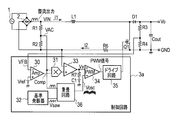
- FIG. 1 is a circuit configuration diagram of a conventional power factor correction circuit.
- the continuous current mode power factor correction circuit bridge rectifies the AC voltage of the AC power source 1 by the rectifier 2, converts the rectified rectified output VIN into a DC voltage, and supplies the output voltage Vo to a load (not shown). , Improve power factor.
- the power factor correction circuit is a step-up type power factor correction circuit and includes a coil L1, a switching element Q1, a first diode D1, an output capacitor Cout, and a control circuit 3A.
- the PFC circuit outputs a high-frequency switching control signal from the control circuit 3A to the switching element Q1, and controls the switching element Q1 on / off at a high frequency.
- the current flowing through the coil L1 is turned on / off at a high frequency to improve the power factor, and the output voltage Vo of the PFC circuit is boosted.
- the control circuit 3A includes an error amplifier 30, a multiplier 31, a reference oscillator 32, a calculator 33, a PWM comparator 34, and a drive circuit 35.
- the error amplifier 30 amplifies an error voltage between the feedback voltage VFB, which is a voltage obtained by dividing the output voltage Vo by the resistors R3 and R4, and the reference voltage Vref, and outputs the amplified voltage as an output voltage Comp.
- the multiplier 31 multiplies the rectified divided voltage VAC obtained by dividing the rectified output VIN rectified by the rectifier 2 by the resistors R1 and R2 by the output voltage Comp of the error amplifier 30, and the obtained value is multiplied by the input current. The target value.
- the current detection resistor R6 outputs a voltage corresponding to the current flowing through the switching element Q1 to the inverting input terminal of the calculator 33.
- the calculator 33 calculates a voltage corresponding to the current detected by the current detection resistor R 6 from the multiplication output from the multiplier 31, and outputs the signal Vx to the non-inverting input terminal of the PWM comparator 34.
- a series circuit of a resistor R7 and a capacitor C1 is connected to the output of the calculator 33 for phase correction.
- the PWM comparator 34 compares the signal Vx from the calculator 33 and the sawtooth signal Vsaw from the reference oscillator 32 and controls so that a current similar to the input voltage is generated and the power factor correction operation is performed.
- the duty of the switching element Q1 becomes an appropriate value by the feedback control.
- the control circuit 3 detects the output voltage Vo and controls the duty of the switching element Q1 based on the output voltage Vo, thereby causing the output voltage Vo to have a predetermined value.
- the control circuit 3A uses the resistor R7, which is a phase correction circuit of the arithmetic unit 33, and the capacitor C1 so that the average value of the input current I1 is similar to the rectified output VIN. Response time due to constant delay is required. For this reason, the average value of the input current I1 is similar to the rectified output VIN, which is delayed by the response time.
- Patent Document 2 since the fluctuation of the input voltage is input to the feedback loop of the output voltage, the response time of the output voltage when the input voltage fluctuates becomes short, but the delay of the input current I1 that leads to power factor improvement. could not be improved.
- An object of the present invention is to provide a power factor correction circuit and a DC / DC converter that can achieve both high power factor and improved stability with a simple configuration.
- a power factor correction circuit includes a rectifier circuit that rectifies an AC voltage of an AC power supply, a series circuit including a coil and a switching element connected in series to an output terminal of the rectifier circuit.
- a rectifying / smoothing circuit comprising a rectifying element and a smoothing capacitor connected in series between the main electrode of the circuit, the switching element, an error voltage between an output voltage of the smoothing capacitor and a reference voltage, and an output of the rectifying circuit;
- An arithmetic unit that calculates a multiplication voltage obtained by multiplying the current by the switching element or a voltage corresponding to a current from the output terminal of the rectifier circuit, a reference oscillator that generates a reference signal, and an output of the rectifier circuit
- a superposition circuit that superimposes a signal based on the reference signal of the reference oscillator, and generates a pulse signal by comparing the output of the superposition circuit with the output from the computing unit And a control circuit for turning on / off the switching element by the pulse signal.
- the control circuit performs feedback control based on the error voltage between the output voltage of the smoothing capacitor and the reference voltage, and compares the signal based on the output of the rectifier circuit with the output of the reference signal and the error voltage.
- FIG. 1 is a circuit configuration diagram of a conventional power factor correction circuit.
- FIG. 2 is a circuit configuration diagram of the power factor correction circuit according to the first embodiment.
- FIG. 3 is a circuit configuration diagram of a superposition circuit provided in the power factor correction circuit according to the first embodiment.
- FIG. 4 is a waveform diagram of each part for explaining the operation of the PWM comparator of the conventional power factor correction circuit.
- FIG. 5 is a waveform diagram of each part for explaining the operation of the PWM comparator of the power factor correction circuit according to the first embodiment.
- FIG. 6 is a circuit configuration diagram of a power factor correction circuit according to the second embodiment.
- FIG. 7 is a circuit configuration diagram of the power factor correction circuit according to the third embodiment.
- FIG. 8 is a circuit configuration diagram of a superposition circuit provided in the power factor correction circuit according to the third embodiment.
- FIG. 9 is a circuit configuration diagram of the power factor correction circuit according to the fourth embodiment.
- FIG. 10 is a circuit configuration diagram of a superposition circuit provided in the power factor correction circuit according to the fourth embodiment.
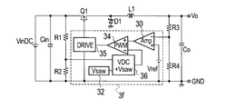
- FIG. 11 is a circuit configuration diagram of the step-up DC / DC converter according to the fifth embodiment.
- FIG. 12 is a circuit configuration diagram of the step-down DC / DC converter according to the sixth embodiment.
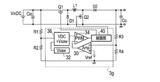
- FIG. 13 is a circuit configuration diagram of the step-up / step-down DC / DC converter according to the seventh embodiment.
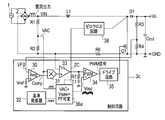
- FIG. 2 is a circuit configuration diagram of the power factor correction circuit according to the first embodiment.
- the power factor correction circuit is a step-up power factor correction circuit, and includes an AC power source 1, a rectifier 2, a coil L1, a switching element Q1, a first diode D1, an output capacitor Cout, and a control circuit 3a.
- the rectifier 2 full-wave rectifies the AC voltage input from the AC power supply 1 and outputs a rectified output VIN.
- the resistors R1 and R2 output a rectified and divided output VAC obtained by dividing the rectified output VIN by resistance.
- the output terminal of the rectifier 1 is connected in series with a coil L1 and a switching element Q1 made of a MOSFET.
- the anode of the diode D1 is connected to the connection point between the coil L1 and the switching element Q1, and the cathode of the diode D1 is grounded via the smoothing capacitor Co.
- a series circuit of a resistor R1 and a resistor R2 is connected to the output terminal of the rectifier 2 as a voltage dividing resistor.
- a series circuit of a resistor R3 and a resistor R4 is connected to both ends of the smoothing capacitor Co as a voltage dividing resistor.
- the control circuit 3a inputs the rectified voltage divided output VAC based on the voltage dividing ratio between the resistor R1 and the resistor R2 and the feedback voltage VFB based on the voltage dividing ratio between the resistor R3 and the resistor R4, and inputs the rectified voltage divided output VAC and the feedback voltage VFB. Based on the above, a drive signal is generated, and the drive signal is output to the gate of the switching element Q1.
- the voltage dividing ratio for obtaining the rectified divided output VAC and the feedback voltage VFB is preferably set to be equal to each other from a feedforward operation described later.
- a current detection resistor R6 is connected between the terminal connected to the ground GND of the switching element Q1 and the resistor R2.
- the current detection resistor R6 converts the current I2 flowing between the GND side terminal of the switching element Q1 and the resistor R2 into a voltage, and outputs the converted voltage to the inverting terminal of the calculator 33.
- the current I2 is the same as the output current I1 of the rectifier 2 that is the input current of the PFC.
- the control circuit 3a includes an error amplifier 30, a multiplier 31, a reference oscillator 32, a calculator 33, a PWM comparator 34, a drive circuit 35, and a superimposing circuit 36.
- the error amplifier 30 amplifies an error voltage between the feedback voltage VFB, which is a voltage obtained by dividing the output voltage Vo by the resistor R3 and the resistor R4, and the reference voltage Vref, and outputs the amplified voltage as an output voltage Comp.
- the multiplier 31 multiplies the rectified divided output VAC obtained by dividing the rectified output VIN rectified by the rectifier 2 with the resistors R1 and R2 by the output voltage Comp of the error amplifier 30, and the obtained value is multiplied by the input current. The target value.
- the current detection resistor R6 outputs a voltage corresponding to the current flowing through the switching element Q1 to the inverting input terminal of the calculator 33.
- the calculator 33 calculates a voltage corresponding to the current detected by the current detection resistor R 6 from the multiplication output from the multiplier 31, and outputs the signal Vx to the non-inverting input terminal of the PWM comparator 34.
- a series circuit of a resistor R7 and a capacitor C1 is connected to the output of the calculator 33 for phase correction.
- the reference oscillator 32 generates a sawtooth signal Vsaw that is a reference signal, and outputs the sawtooth signal Vsaw to the superposition circuit 36.
- the superimposing circuit 36 superimposes the sawtooth wave signal Vsaw from the reference oscillator 32 on the rectified divided output VAC obtained by dividing the rectified output VIN rectified by the rectifier 2 by the resistors R1 and R2, and the PWM comparator 34 as the superimposed signal Vosc. Output to the inverting input terminal.
- the PWM comparator 34 corresponds to the control circuit of the present invention, generates a pulse signal PWM by comparing the signal Vx from the computing unit 33 and the superimposed signal Vosc from the superimposing circuit 36, and outputs the pulse signal PWM to the drive circuit 35. . That is, the PWM comparator 34 can perform feedforward control by comparing the superimposed signal Vosc and the signal Vx, and can reduce the phase correction of the calculator 33. Details of the feedforward control will be described later.
- the drive circuit 35 turns on and off the switching element Q1 by applying a drive signal to the gate of the switching element Q1.
- the PWM comparator 34 can control the output voltage Vo to be constant by controlling the duty that is the on / off ratio of the switching element Q1.
- FIG. 3 is a circuit configuration diagram of the superposition circuit 36.
- the superimposing circuit 36 includes a current mirror circuit 361, an operational amplifier OP1, a resistor Ra, a resistor Rb, a resistor Rc, an N-type MOSFET Qa, a PNP bipolar transistor Qb, and an NPN bipolar transistor Qc.
- the rectified and divided output VAC is input to the non-inverting input of the operational amplifier OP1.
- the inverting input terminal of the operational amplifier OP1 is connected to the source of the MOSFET Qa and grounded through the resistor Ra.
- the output of the operational amplifier OP1 is connected to the gate of the MOSFET Qa, and the drain is connected to the current mirror circuit 361.
- a power supply Vcc is applied to the current mirror circuit 361.
- the drain current of the MOSFET Qa flows through the current mirror circuit 361 to the resistor Rb and the transistor Qb connected in series.
- the emitter of the transistor Qb is connected to the resistor Rb, and the collector of the transistor Qb is grounded.
- the sawtooth signal Vsaw is input from the reference oscillator 32 to the base of the transistor Qb.
- the base of the transistor Qc is connected to the connection point between the resistor Rb and the current mirror circuit 361.
- the collector of the transistor Qc is connected to the power supply Vcc, the emitter of the transistor Qc is connected to one end of the resistor Rc, and the other end of the resistor Rc is grounded.
- the emitter of the transistor Qc serves as the output terminal of the superposition circuit 36 and outputs a superposition signal Vosc.
- the rectified voltage-divided output VAC is converted into a current by the resistor Ra, and the converted current is converted into a voltage by the resistor Rb via the current mirror circuit 361.
- the voltage VFF of the resistor Rb is expressed by Expression (1).
- the superposition signal Vosc is a voltage obtained by adding the voltage VFF to the sawtooth wave output Vsaw, and this voltage is expressed by Expression (2).
- the voltage VBE1 is the base-emitter voltage of the transistor Qb
- VBE2 is the base-emitter voltage of the transistor Qc.
- the multiplier 31 multiplies the rectified divided output VAC and the output voltage Comp of the error amplifier 30, and the calculator 33 calculates the current output from the rectifier 2 from the output value of the multiplier 31.
- the voltage Vx is obtained by calculation.
- the PWM comparator 34 compares the voltage Vx with the sawtooth wave output Vsaw.
- a current similar to the input voltage is generated by comparing the value obtained by multiplying the rectified voltage-divided output VAC and the output voltage Comp with the GND current I2, and the power factor improving operation is performed.
- the duty of the switching element Q1 becomes an appropriate value by feedback control, and the duty during the CCM operation is determined from the rectified output VIN and the output voltage Vo.
- the burden of the feedback control can be reduced, and the operation can be performed more stably and at high speed.
- feedforward control will be described.
- FIG. 4 The operation waveform of the conventional control is shown in FIG. 4, and the operation waveform of the control of the present invention is shown in FIG. 4A and 5A show the rectified output VAC.
- FIG. 4B shows the sawtooth wave output Vsaw and the non-inverted input signal Vx of the PWM comparator 34.
- 4C and 5C show the output OUT of the PWM comparator 34.
- FIG. FIG. 4D and FIG. 5D show the PWM comparator 34.
- Va is a lower limit value of the sawtooth wave output Vsaw
- Vb is an upper limit value of the sawtooth wave output Vsaw
- Doff is an off duty of the PWM comparator output
- VFB is a voltage obtained by dividing the output voltage Vo by the resistors R3 and R4.
- the signal Vx changes with the change of the rectified and divided output VAC.
- the signal Vx is delayed with respect to the rectified and divided output VAC due to the effect of phase correction by the phase correction circuits R7 and C1 of the calculator 33. . For this reason, responsiveness falls and a power factor falls.
- the control of the present invention by setting the signal Vx to a constant value or a substantially constant value, even if there is a delay due to the phase correction, the influence of the delay on the rectified divided output VAC of the signal Vx does not occur. That is, responsiveness is improved.
- the signal Vx and the sawtooth wave output Vsaw are compared by the PWM comparator 34, and the average value of the input current I1 is controlled to be similar to the rectified output VIN.
- the duty of the switching element Q1 is determined by the ratio between the rectified output VIN and the output voltage Vo.
- the rectified output VIN varies because it becomes a voltage obtained by rectifying the AC voltage AC.
- the signal Vx also varies.
- the superimposed signal Vosc is changed by superimposing the rectified voltage divided output VAC synchronized with the rectified output VIN on the sawtooth wave output Vsaw from the reference oscillator 32.
- the signal Vx is a constant value, the response characteristic is improved even if there is a phase lag between the resistor R7 and the capacitor C1. For this reason, even if the signal Vx is a constant value, the duty of the switching element Q1 is controlled so that the output voltage Vo is constant.
- the VAC component that changes due to the AC waveform is canceled, and the signal Vx is not dependent on the commercial AC waveform as shown in the equation (12). May be the upper limit value Vb of the sawtooth wave output Vsaw. That is, the target duty is obtained by the constant signal Vx.
- a feedforward signal can be generated for the duty control of the CCMPFC by adding a relatively easy superimposing circuit 36.
- feed-forward control By adding feed-forward control, the amount of feedback gain can be reduced and operation can be performed stably and at high speed.
- the signal Vx which is the input signal of the PWM comparator 34, has a waveform similar to the rectified output VAC.
- the signal Vx becomes a voltage close to a DC voltage and is appropriately controlled. Since the signal Vx is a voltage close to a DC voltage, the influence of phase correction is reduced, and the responsiveness is improved. For this reason, in the first embodiment, even when the phase correction is shallower than that of the conventional control method, it is possible to ensure equal or better response.
- the power factor is also improved compared to the conventional control because the influence of phase correction is small.
- FIG. 5 is a circuit configuration diagram of a power factor correction circuit according to the second embodiment.
- the current I2 is detected by the current detection resistor R6, and the detected current is converted into a voltage.
- the efficiency decreases.
- the power factor correction circuit according to the second embodiment is characterized in that current detection is performed using a current transformer T1.
- the current transformer T1 has a primary winding P1 and a secondary winding S1, and the turns ratio of the primary winding P1 and the secondary winding S1 is 1: N.
- the primary winding P1 is connected between the coil L1 and the drain of the switching element Q1.
- a series circuit of a diode D2 and a resistor R5 is connected to both ends of the primary winding P1, and a signal CS1 at a connection point between the diode D2 and the resistor R5 is output to the current-voltage conversion circuit 37 of the control circuit 3.
- the transformer T1, the diode D2, and the resistor R5 constitute a current detector that detects a current flowing through the switching element Q1.
- the current-voltage conversion circuit 32 outputs a voltage VL proportional to the current detected by the current detector to the inverting input terminal of the calculator 33.
- FIG. 7 is a circuit configuration diagram of the power factor correction circuit according to the third embodiment.
- the power factor correction circuit according to the third embodiment is characterized in that a zero cross circuit 38 is provided.
- the zero-cross circuit 38 is connected to the connection point between the coil L1 and the diode D1, and determines whether the current flowing through the coil L1 is a continuous region or a discontinuous region by detecting the voltage at the connection point between the coil L1 and the diode D1. Then, the determination output is output to the superimposing circuit 36a.
- the zero cross circuit 38 corresponds to the region determination unit of the present invention.
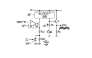
- FIG. 8 is a circuit configuration diagram of the superposition circuit 36a provided in the power factor correction circuit according to the third embodiment.
- the superimposing circuit 36a switches the ratio of superimposing the signal based on the output of the rectifier circuit 2 on the reference signal of the reference oscillator 32 according to the continuous region and the discontinuous region.
- the superimposing circuit 36a has a resistor Ra1 and a resistor Ra2 connected in series to the source of the MOSFET Qa.
- a switch SW1 is connected in parallel to both ends of the resistor Ra2.
- FIG. 9 is a circuit configuration diagram of a power factor correction circuit according to the fourth embodiment.
- the power factor correction circuit according to the fourth embodiment is characterized in that a current detection circuit 39 is provided.
- the current detection circuit 39 is connected to the current detection resistor R6, and detects the load current by the current detection resistor R6.
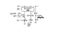
- FIG. 10 is a circuit configuration diagram of the superposition circuit 36b provided in the power factor correction circuit according to the fourth embodiment.
- the superimposing circuit 36b has a variable resistor Rx connected to the drain of the MOSFET Qa, and varies the feedforward amount that is a ratio of superimposing a signal based on the output of the rectifying circuit 2 on the reference signal of the reference oscillator 32.
- the variable resistor Rx varies the resistance value so that the feedforward amount corresponds to the load current detected by the current detection circuit 39. Thereby, the feedforward amount can be set continuously by the current flowing through the coil L1, and the feedforward amount corresponding to the discontinuous amount can be set particularly in the discontinuous region where the current flowing through the coil L1 is discontinuous. . (Example 5) FIG.
- FIG. 11 is a circuit configuration diagram of the step-up DC / DC converter according to the fifth embodiment.
- the fifth embodiment is characterized in that the AC power source 1 that is the input power source of the first embodiment is changed to a DC power source Vin.
- An input capacitor Cin is connected in parallel to both ends of the DC power supply Vin, and a series circuit of a resistor R1 and a resistor R2 is connected in parallel.
- the superimposing circuit 36 superimposes a signal based on the output of the DC power source Vin on the reference signal of the reference oscillator 32.
- the PWM comparator 34 generates a pulse signal by comparing the error voltage between the output voltage of the smoothing capacitor Co and the reference voltage Vref and the output of the superposition circuit 36, and turns on / off the switching element Q1 by the pulse signal.
- the input voltage is a commercial AC voltage and the boost type PFC control is described.
- the input voltage may be a DC voltage. Even when the input voltage is a DC voltage, the response of the output voltage is improved by feedforward control in which the input voltage is superimposed on the sawtooth wave output even when the input power supply is momentarily interrupted or fluctuates due to load regulation.
- FIG. 12 illustrates a step-down DC / DC converter circuit according to the sixth embodiment.
- the source of the switching element Q1 is connected to the output terminal of the DC power source Vin, and the cathode of the diode D1 and one end of the coil L1 are connected to the drain of the switching element Q1.
- FIG. 13 is a step-up / step-down DC / DC converter circuit according to the seventh embodiment.
- the switching element Q1 and the coil L1 are connected in series to the output terminal of the DC power supply Vin, the diode D1 is connected to the connection point between the switching element Q1 and the coil L1, and the coil L1 and the diode D2 are connected.
- Switching element Q2 is connected to the connection point.
- the control unit 40 generates the first pulse signal and the second pulse signal by comparing the error voltage between the output voltage of the smoothing capacitor Co and the reference voltage Vref and the output of the superposition circuit 36, and the switching element is generated by the first pulse signal.
- Q1 is turned on / off
- the switching element Q2 is turned on / off by the second pulse signal.
- the present invention is not limited to the power factor correction circuits and DC / DC converters of the first to seventh embodiments.
- the switching element Q1 is a MOSFET, but it may be a semiconductor switch other than a MOSFET, such as an IGBT or a bipolar transistor.
- the rectifying element is a diode, but a semiconductor switch other than the diode may be used.
- the present invention is applicable to a DC / DC converter.
Landscapes
- Engineering & Computer Science (AREA)
- Power Engineering (AREA)
- Dc-Dc Converters (AREA)
- Rectifiers (AREA)
Abstract
本発明は、整流回路2の出力端子に接続されたコイルL1とスイッチング素子Q1とからなる直列回路と、整流素子D1と平滑コンデンサCoとからなる整流平滑回路と、平滑コンデンサの出力電圧と基準電圧との誤差電圧と整流回路の出力とを乗算した乗算電圧と、スイッチング素子に流れる電流又は整流回路の出力端子からの電流に対応する電圧とを演算する演算器33と、整流回路の出力に基づく信号を基準発振器32の基準信号に重畳させる重畳回路36と、重畳回路の出力と演算器からの出力と比較することによりパルス信号を生成しパルス信号によりスイッチング素子をオン/オフさせる制御回路34とを備える。
Description
本発明は、高力率で安定性の高い力率改善回路及びDC/DCコンバータに関する。
従来の電流連続モード力率改善回路(CCMPFC)は、特許文献1に記載されるように、出力電圧を検出し、検出された出力電圧に基づいて力率改善制御を行っている。
また、従来のCCMPFCは、特許文献2に記載されるように、入力電圧変動の応答性を向上させるために、入力電圧の変動を出力電圧のフィードバックループに入力し、出力電圧を制御している。
図1は、従来の力率改善回路の回路構成図である。図1において、電流連続モード力率改善回路は、交流電源1の交流電圧を整流器2によりブリッジ整流し、整流された整流出力VINを直流電圧に変換して出力電圧Voを図示しない負荷に供給し、力率改善を行う。
図1に示すように力率改善回路(PFC)は、昇圧型力率改善回路であり、コイルL1、スイッチング素子Q1、第1のダイオードD1および出力コンデンサCout、制御回路3Aを備える。また、PFC回路は、制御回路3Aからスイッチング素子Q1に高周波スイッチング制御信号を出力し、スイッチング素子Q1を高周波でオン/オフ制御する。これにより、コイルL1に流れる電流が高周波でオン/オフされて力率が改善されるとともに、PFC回路の出力電圧Voが昇圧される。
図1に示すように、制御回路3Aは、誤差増幅器30、乗算器31、基準発振器32、演算器33、PWMコンパレータ34、ドライブ回路35を備える。誤差増幅器30は、出力電圧Voを抵抗R3と抵抗R4とで分圧した電圧であるフィードバック電圧VFBと基準電圧Vrefとの誤差電圧を増幅して出力電圧Compとして出力する。乗算器31は、整流器2で整流した整流出力VINを抵抗R1と抵抗R2で分圧した整流分圧電圧VACと、誤差増幅器30の出力電圧Compとを乗算し、得られた値を入力電流の目標値とする。
電流検出抵抗R6は、スイッチング素子Q1に流れる電流に対応する電圧を演算器33の反転入力端子に出力する。演算器33は、乗算器31からの乗算出力から、電流検出抵抗R6で検出された電流に対応する電圧を演算し、信号VxをPWMコンパレータ34の非反転入力端子に出力する。演算器33の出力には、位相補正用に抵抗R7とコンデンサC1との直列回路が接続される。
入力電圧に相似な電流を生成し力率改善動作になるように、PWMコンパレータ34は、演算器33からの信号Vxと基準発振器32からの鋸波信号Vsawとを比較し制御する。スイッチング素子Q1のデューティは、上記フィードバック制御により、適切な値になる。制御回路3は、出力電圧Voを検出し、出力電圧Voに基づきスイッチング素子Q1のデューティを制御することにより出力電圧Voを所定値にさせる。
しかしながら、制御回路3Aは、整流出力VINを検出してから、入力電流I1の平均値が、整流出力VINと相似にさせるために、演算器33の位相補正回路である抵抗R7、コンデンサC1の時定数の遅れによる応答時間が必要となる。このため、入力電流I1の平均値が、整流出力VINと相似になるのが、応答時間分、遅れる。
応答時間を早くするためには、演算器33の位相補正回路である抵抗R7、コンデンサC1の時定数を調整し、応答時間を短くする必要がある。しかし、演算器33の位相補正を調整するため、安定性が低下する。
また、特許文献2では、入力電圧の変動を出力電圧のフィードバックループに入力しているため、入力電圧変動時の出力電圧の応答時間は、短くなるが、力率改善につながる入力電流I1の遅れは、改善することができなかった。
本発明の課題は、簡易な構成により高力率と安定性の向上とを両立することができる力率改善回路及びDC/DCコンバータを提供することである
前記課題を解決するために、本発明の力率改善回路は、交流電源の交流電圧を整流する整流回路と、前記整流回路の出力端子に、直列に接続されたコイルとスイッチング素子とからなる直列回路と、前記スイッチング素子の主電極間に、直列に接続された整流素子と平滑コンデンサとからなる整流平滑回路と、前記平滑コンデンサの出力電圧と基準電圧との誤差電圧と前記整流回路の出力とを乗算した乗算電圧と、前記スイッチング素子に流れる電流又は前記整流回路の出力端子からの電流に対応する電圧とを演算する演算器と、基準信号を発生する基準発振器と、前記整流回路の出力に基づく信号を前記基準発振器の基準信号に重畳させる重畳回路と、前記重畳回路の出力と前記演算器からの出力と比較することによりパルス信号を生成し前記パルス信号により前記スイッチング素子をオン/オフさせる制御回路とを備える。
本発明によれば、制御回路は、平滑コンデンサの出力電圧と基準電圧との誤差電圧によるフィードバック制御と、整流回路の出力に基づく信号を基準信号の出力に重畳させた信号と誤差電圧との比較によるフィードフォワード制御とを組み合わせることで、高力率と安定性の向上とを両立することができる。
以下に、本発明の力率改善回路及びDC/DCコンバータの実施例を、図面を参照しながら、説明する。ここでは、力率改善回路として、電流連続モード力率改善回路を説明する。
(実施例1)
図2は、実施例1の力率改善回路の回路構成図である。図2において、力率改善回路は、昇圧型力率改善回路であり、交流電源1、整流器2、コイルL1、スイッチング素子Q1、第1のダイオードD1および出力コンデンサCout、制御回路3aを備える。
(実施例1)
図2は、実施例1の力率改善回路の回路構成図である。図2において、力率改善回路は、昇圧型力率改善回路であり、交流電源1、整流器2、コイルL1、スイッチング素子Q1、第1のダイオードD1および出力コンデンサCout、制御回路3aを備える。
整流器2は、交流電源1から入力された交流電圧を全波整流し整流出力VINを出力し、抵抗R1と抵抗R2とは、整流出力VINを抵抗分圧した整流分圧出力VACを出力する。
整流器1の出力端には、コイルL1とMOSFETからなるスイッチング素子Q1とが直列に接続される。コイルL1とスイッチング素子Q1との接続点にはダイオードD1のアノードが接続され、ダイオードD1のカソードは、平滑コンデンサCoを介して接地されている。
整流器2の出力端には、分圧抵抗として、抵抗R1と抵抗R2との直列回路が接続されている。また、平滑コンデンサCoの両端には、分圧抵抗として、抵抗R3と抵抗R4との直列回路が接続されている。
制御回路3aは、抵抗R1と抵抗R2との分圧比に基づく整流分圧出力VACと抵抗R3と抵抗R4との分圧比に基づくフィードバック電圧VFBとを入力し、整流分圧出力VACとフィードバック電圧VFBとに基づき駆動信号を生成して、スイッチング素子Q1のゲートに駆動信号を出力する。整流分圧出力VACとフィードバック電圧VFBとを得るための分圧比は、後述のフィードフォワードの動作から互いに等しく設定されることが好ましい。
スイッチング素子Q1のグランドGNDに接続される端子と抵抗R2の間には、電流検出抵抗R6が接続されている。電流検出抵抗R6は、スイッチング素子Q1のGND側端子と抵抗R2間に流れる電流I2を電圧に変換し、変換された電圧を演算器33の反転端子に出力する。尚、電流I2は、PFCの入力電流である整流器2の出力電流I1と同じ電流が流れる。
制御回路3aは、誤差増幅器30、乗算器31、基準発振器32、演算器33、PWMコンパレータ34、ドライブ回路35、重畳回路36を備える。
誤差増幅器30は、出力電圧Voを抵抗R3と抵抗R4とで分圧した電圧であるフィードバック電圧VFBと基準電圧Vrefとの誤差電圧を増幅して出力電圧Compとして出力する。乗算器31は、整流器2で整流した整流出力VINを抵抗R1と抵抗R2で分圧した整流分圧出力VACと、誤差増幅器30の出力電圧Compとを乗算し、得られた値を入力電流の目標値とする。
電流検出抵抗R6は、スイッチング素子Q1に流れる電流に対応する電圧を演算器33の反転入力端子に出力する。演算器33は、乗算器31からの乗算出力から、電流検出抵抗R6で検出された電流に対応する電圧を演算し、信号VxをPWMコンパレータ34の非反転入力端子に出力する。演算器33の出力には、位相補正用に抵抗R7とコンデンサC1との直列回路が接続される。
基準発振器32は、基準信号である鋸波信号Vsawを発生し、鋸波信号Vsawを重畳回路36に出力する。重畳回路36は、整流器2で整流した整流出力VINを抵抗R1と抵抗R2で分圧した整流分圧出力VACに、基準発振器32からの鋸波信号Vsawを重畳し、重畳信号VoscとしてPWMコンパレータ34の反転入力端子に出力する。
PWMコンパレータ34は、本発明の制御回路に対応し、演算器33からの信号Vxと重畳回路36からの重畳信号Voscとを比較することにより、パルス信号PWMを生成してドライブ回路35に出力する。即ち、PWMコンパレータ34は、重畳信号Voscと信号Vxと比較することでフィードフォワード制御を行い、演算器33の位相補正を浅くすることができる。フィードフォワード制御の詳細は、後述する。
ドライブ回路35は、駆動信号をスイッチング素子Q1のゲートに印加することで、スイッチング素子Q1をオンオフさせる。PWMコンパレータ34は、スイッチング素子Q1のオンオフ比であるデューティを制御することで、出力電圧Voを一定に制御することができる。
図3は重畳回路36の回路構成図である。重畳回路36は、カレントミラー回路361、オペアンプOP1、抵抗Ra、抵抗Rb、抵抗Rc、N型のMOSFETQa,PNPバイポーラ型のトランジスタQb、NPNバイポーラ型のトランジスタQcを備える。
オペアンプOP1の非反転入力には、整流分圧出力VACが入力される。オペアンプOP1の反転入力端子は、MOSFETQaのソースに接続され、抵抗Raを介して接地される。オペアンプOP1の出力は、MOSFETQaのゲートに接続され、ドレインはカレントミラー回路361に接続される。カレントミラー回路361には、電源Vccが印加されている。
MOSFETQaのドレイン電流は、カレントミラー回路361を介して、直列接続された抵抗RbとトランジスタQbに流れる。トランジスタQbのエミッタは、抵抗Rbに接続され、トランジスタQbのコレクタは接地される。トランジスタQbのベースには、基準発振器32から鋸波信号Vsawが入力される。
抵抗Rbとカレントミラー回路361との接続点には、トランジスタQcのベースが接続される。トランジスタQcのコレクタは、電源Vccに接続され、トランジスタQcのエミッタは、抵抗Rcの一端に接続され、抵抗Rcの他端は接地される。トランジスタQcのエミッタは、重畳回路36の出力端となり、重畳信号Voscを出力する。
図3に示す重畳回路36によれば、整流分圧出力VACは、抵抗Raにより電流に変換され、変換された電流は、カレントミラー回路361を介して抵抗Rbにより電圧に変換される。抵抗Rbの電圧VFFは、式(1)で表される。


スイッチング素子Q1のデューティは、フィードバック制御により、適切な値になり、CCM動作時のデューティは整流出力VINと出力電圧Voから決まる。
これに対して、本発明では、さらに、このデューティが自然に決まるフィードフォワード制御を制御回路3aに組み込むことにより、フィードバック制御の負担を減らすことができ、より安定・高速に動作させることができる。以下、フィードフォワード制御について説明する。
以下に、PWMコンパレータ34の入力である信号Vx及び重畳信号Voscと、PWMコンパレータ34の出力との関係を、従来の制御と本発明の制御とで比較する。
従来の制御の動作波形を図4に示し、本発明の制御の動作波形を図5に示す。図4(a)、図5(a)は整流出力VACを示す。図4(b)は鋸波出力Vsaw及びPWMコンパレータ34の非反転入力信号Vxを示す。図5(b)は重畳信号Vosc(=Vsaw+VFF)と信号Vxを示す。図4(c)、図5(c)はPWMコンパレータ34の出力OUTを示す。図4(d)、図5(d)はPWMコンパレータ34を示す。
また、Vaは鋸波出力Vsawの下限値、Vbは鋸波出力Vsawの上限値、DoffはPWMコンパレータ出力のオフデューティ,VFBは出力電圧Voを抵抗R3と抵抗R4とで抵抗分圧された電圧とする。
従来の制御では、式(4)に示すように、整流分圧出力VACの変化に伴い、信号Vxが変化する。




これに対して、本発明の制御では、信号Vxを一定値又は略一定値にすることにより、位相補正による遅れがあっても、信号Vxの整流分圧出力VACに対する遅れの影響が発生しない。即ち、応答性が良くなる。
従来のCCMPFCでは、信号Vxと鋸波出力VsawとがPWMコンパレータ34により比較され、入力電流I1の平均値は整流出力VINと相似になるように制御される。スイッチング素子Q1のデューティは、整流出力VINと出力電圧Voとの比で決定される。整流出力VINは、交流電圧ACを整流した電圧となることから変動する。この整流電圧である整流出力VINの変動に伴い、信号Vxも変動する。
これに対して、実施例1では、図5(b)に示すように、基準発振器32からの鋸波出力Vsawに整流出力VINと同期した整流分圧出力VACを重畳させて重畳信号Voscを変動させ、信号Vxを一定値にさせる。信号Vxが一定値であるため、抵抗R7とコンデンサC1との位相遅れがあっても、応答特性が良くなる。このため、信号Vxが一定値でも、スイッチング素子Q1のデューティは、出力電圧Voが一定になるように制御される。
次に、鋸波出力VsawにVFF信号を加えた場合、信号Vxが一定値になる方法を計算式から導く。





このように、従来の制御では、図4に示すように、PWMコンパレータ34の入力信号である信号Vxが、整流出力VACと相似に近い波形になっている。本発明の制御では、フィードフォワード制御を追加することで、図5に示すように、信号Vxは、重畳信号Vosc=Vsaw+VFFと比較される。これにより、信号Vxは、直流電圧に近い電圧となり、適切に制御される。信号Vxは、直流電圧に近い電圧となるため、位相補正の影響が小さくなり、応答性が改善される。このため、実施例1では、従来の制御方式に比べ、位相補正を浅くしても、同等以上の応答性が確保できる。力率についても、位相補正の影響が小さいため、従来の制御に比べ、改善される。
仮に、フィードフォワード回路である重畳回路36が故障し、フィードフォワード量が大きくなった場合には、スイッチング素子Q1のオンデューティは、狭くなる。このため、出力電圧Voが低下することから、安全方向となる。また、フィードフォワード量が小さくなった場合には、フィードフォワードがない、PFCとして動作する。このため、力率、安定性が低下するが、PFC制御となるため、問題はない。
なお、本発明は、CCMPFCとして記載しているが、電流不連続モード力率改善回路(DCMPFC)でも、フィードフォワード量を低下させることで、制御可能である。CCMPFCでも、負荷電流が小さい場合、DCMPFCとなる。DCM領域での制御が必要な場合には、フィードフォワード量を低下させた制御を行う。
(実施例2)
図5は、実施例2の力率改善回路の回路構成図である。実施例1の力率改善回路は、電流検出抵抗R6により電流I2を検出して検出された電流を電圧に変換していた。しかし、電流検出抵抗R6により電流を電圧に変換すると、効率が低下する。実施例2の力率改善回路は、カレントトランスT1を用い、電流検出を行うことを特徴とする。
(実施例2)
図5は、実施例2の力率改善回路の回路構成図である。実施例1の力率改善回路は、電流検出抵抗R6により電流I2を検出して検出された電流を電圧に変換していた。しかし、電流検出抵抗R6により電流を電圧に変換すると、効率が低下する。実施例2の力率改善回路は、カレントトランスT1を用い、電流検出を行うことを特徴とする。
カレントトランスT1は、一次巻線P1と二次巻線S1とを有し、一次巻線P1と二次巻線S1との巻数比は、1:Nである。一次巻線P1は、コイルL1とスイッチング素子Q1のドレインとの間に接続されている。一次巻線P1の両端には、ダイオードD2と抵抗R5との直列回路が接続され、ダイオードD2と抵抗R5との接続点における信号CS1は制御回路3の電流電圧変換回路37に出力される。トランスT1とダイオードD2と抵抗R5とは、スイッチング素子Q1に流れる電流を検出する電流検出器を構成する。電流電圧変換回路32は、電流検出器で検出した電流に比例した電圧VLを演算器33の反転入力端子に出力する。
このように実施例2の力率改善回路によれば、カレントトランスT1を用い、電流検出を行うので、実施例1の力率改善回路よりも効率が良くなる。
(実施例3)
図7は、実施例3の力率改善回路の回路構成図である。実施例3の力率改善回路は、ゼロクロス回路38を設けたことを特徴とする。ゼロクロス回路38は、コイルL1とダイオードD1との接続点に接続され、コイルL1とダイオードD1の接続点の電圧を検出することで、コイルL1に流れる電流が連続領域か、不連続領域かを判定し、判定出力を重畳回路36aに出力する。ゼロクロス回路38は、本発明の領域判定部に対応する。
(実施例3)
図7は、実施例3の力率改善回路の回路構成図である。実施例3の力率改善回路は、ゼロクロス回路38を設けたことを特徴とする。ゼロクロス回路38は、コイルL1とダイオードD1との接続点に接続され、コイルL1とダイオードD1の接続点の電圧を検出することで、コイルL1に流れる電流が連続領域か、不連続領域かを判定し、判定出力を重畳回路36aに出力する。ゼロクロス回路38は、本発明の領域判定部に対応する。
図8は、実施例3の力率改善回路に設けられた重畳回路36aの回路構成図である。重畳回路36aは、連続領域、不連続領域によって、整流回路2の出力に基づく信号を基準発振器32の基準信号に重畳させる比率を切り替える。重畳回路36aは、図8に示すように、MOSFETQaのソースに抵抗Ra1と抵抗Ra2とが直列に接続されている。抵抗Ra2の両端には並列にスイッチSW1が接続されている。
スイッチSW1は、ゼロクロス回路38の判定出力により、オンオフする。スイッチSW1がオンすると、MOSFETQaのドレイン電流が大きくなり、重畳信号Voscが大きくなる。また、スイッチSW1がオフすると、MOSFETQaのドレイン電流が小さくなり、重畳信号Voscが小さくなる。即ち、スイッチSW1がオンオフすることで、フィードフォワード量を切り替えている。これにより、コイルL1に流れる電流が連続領域か、不連続領域かによって、最適なフィードフォワード量を設定することができる。
(実施例4)
図9は、実施例4の力率改善回路の回路構成図である。実施例4の力率改善回路は、電流検出回路39を設けたことを特徴とする。電流検出回路39は、電流検出抵抗R6に接続され、電流検出抵抗R6により負荷電流を検出する。
(実施例4)
図9は、実施例4の力率改善回路の回路構成図である。実施例4の力率改善回路は、電流検出回路39を設けたことを特徴とする。電流検出回路39は、電流検出抵抗R6に接続され、電流検出抵抗R6により負荷電流を検出する。
図10は、実施例4の力率改善回路に設けられた重畳回路36bの回路構成図である。重畳回路36bは、MOSFETQaのドレインに接続された可変抵抗Rxを有し、整流回路2の出力に基づく信号を基準発振器32の基準信号に重畳させる比率であるフィードフォワード量を可変させる。可変抵抗Rxは、電流検出回路39で検出された負荷電流に応じたフィードフォワード量になるように抵抗値を可変させる。これにより、コイルL1に流れる電流で、連続してフィードフォワード量を設定することができ、特にコイルL1に流れる電流が不連続領域では、不連続量に応じたフィードフォワード量を設定することができる。
(実施例5)
図11は、実施例5の昇圧型DC/DCコンバータの回路構成図である。実施例5は、実施例1の入力電源である交流電源1を直流電源Vinに変更したことを特徴とする。直流電源Vinの両端には、入力コンデンサCinが並列に接続されるとともに、抵抗R1と抵抗R2との直列回路が並列に接続される。重畳回路36は、直流電源Vinの出力に基づく信号を基準発振器32の基準信号に重畳させる。PWMコンパレータ34は、平滑コンデンサCoの出力電圧と基準電圧Vrefとの誤差電圧と重畳回路36の出力とを比較することによりパルス信号を生成しパルス信号によりスイッチング素子Q1をオン/オフさせる。実施例1では、入力電圧が商用の交流電圧で、昇圧型のPFC制御について記載しているが、入力電圧は直流電圧でもよい。入力電圧が直流電圧の場合でも、入力電源の瞬断や、ロードレギュレーションで変動した場合についても、鋸波出力に入力電圧を重畳させるフィードフォワードの制御によって、出力電圧の応答性が改善される。実施例5の昇圧型DC/DCコンバータに、実施例3のフィードフォワード量を調整するゼロクロス回路38及びスイッチSW1や、実施例4のフィードフォワード量を調整する電流検出回路39及び可変抵抗Rxを追加してもよい。
(実施例6)
図12は、実施例6の降圧型DC/DCコンバータ回路である。降圧型DC/DCコンバータは、直流電源Vinの出力端にスイッチング素子Q1のソースが接続され、スイッチング素子Q1のドレインにダイオードD1のカソードとコイルL1の一端とが接続されている。降圧型DC/DCコンバータでも、入力電源の瞬断や、ロードレギュレーションで、変動した場合についても、鋸波出力に入力電圧を重畳させるフィードフォワードの制御で、出力電圧の応答性が改善される。実施例6の降圧型DC/DCコンバータに、実施例3のフィードフォワード量を調整するゼロクロス回路38及びスイッチSW1や、実施例4のフィードフォワード量を調整する電流検出回路39及び可変抵抗Rxを追加してもよい。
(実施例7)
図13は、実施例7の昇降圧型DC/DCコンバータ回路である。昇降圧型DC/DCコンバータは、直流電源Vinの出力端にスイッチング素子Q1とコイルL1とが直列に接続され、スイッチング素子Q1とコイルL1との接続点にダイオードD1が接続され、コイルL1とダイオードD2の接続点にスイッチング素子Q2が接続される。制御部40は、平滑コンデンサCoの出力電圧と基準電圧Vrefとの誤差電圧と重畳回路36の出力とを比較することにより第1パルス信号及び第2パルス信号を生成し第1パルス信号によりスイッチング素子Q1をオン/オフさせ、第2パルス信号によりスイッチング素子Q2をオン/オフさせる。昇降圧型DC/DCコンバータでも、入力電源の瞬断や、ロードレギュレーションで、変動した場合についても、鋸波出力に入力電圧を重畳させるフィードフォワードの制御で、出力電圧の応答性が改善される。
(実施例5)
図11は、実施例5の昇圧型DC/DCコンバータの回路構成図である。実施例5は、実施例1の入力電源である交流電源1を直流電源Vinに変更したことを特徴とする。直流電源Vinの両端には、入力コンデンサCinが並列に接続されるとともに、抵抗R1と抵抗R2との直列回路が並列に接続される。重畳回路36は、直流電源Vinの出力に基づく信号を基準発振器32の基準信号に重畳させる。PWMコンパレータ34は、平滑コンデンサCoの出力電圧と基準電圧Vrefとの誤差電圧と重畳回路36の出力とを比較することによりパルス信号を生成しパルス信号によりスイッチング素子Q1をオン/オフさせる。実施例1では、入力電圧が商用の交流電圧で、昇圧型のPFC制御について記載しているが、入力電圧は直流電圧でもよい。入力電圧が直流電圧の場合でも、入力電源の瞬断や、ロードレギュレーションで変動した場合についても、鋸波出力に入力電圧を重畳させるフィードフォワードの制御によって、出力電圧の応答性が改善される。実施例5の昇圧型DC/DCコンバータに、実施例3のフィードフォワード量を調整するゼロクロス回路38及びスイッチSW1や、実施例4のフィードフォワード量を調整する電流検出回路39及び可変抵抗Rxを追加してもよい。
(実施例6)
図12は、実施例6の降圧型DC/DCコンバータ回路である。降圧型DC/DCコンバータは、直流電源Vinの出力端にスイッチング素子Q1のソースが接続され、スイッチング素子Q1のドレインにダイオードD1のカソードとコイルL1の一端とが接続されている。降圧型DC/DCコンバータでも、入力電源の瞬断や、ロードレギュレーションで、変動した場合についても、鋸波出力に入力電圧を重畳させるフィードフォワードの制御で、出力電圧の応答性が改善される。実施例6の降圧型DC/DCコンバータに、実施例3のフィードフォワード量を調整するゼロクロス回路38及びスイッチSW1や、実施例4のフィードフォワード量を調整する電流検出回路39及び可変抵抗Rxを追加してもよい。
(実施例7)
図13は、実施例7の昇降圧型DC/DCコンバータ回路である。昇降圧型DC/DCコンバータは、直流電源Vinの出力端にスイッチング素子Q1とコイルL1とが直列に接続され、スイッチング素子Q1とコイルL1との接続点にダイオードD1が接続され、コイルL1とダイオードD2の接続点にスイッチング素子Q2が接続される。制御部40は、平滑コンデンサCoの出力電圧と基準電圧Vrefとの誤差電圧と重畳回路36の出力とを比較することにより第1パルス信号及び第2パルス信号を生成し第1パルス信号によりスイッチング素子Q1をオン/オフさせ、第2パルス信号によりスイッチング素子Q2をオン/オフさせる。昇降圧型DC/DCコンバータでも、入力電源の瞬断や、ロードレギュレーションで、変動した場合についても、鋸波出力に入力電圧を重畳させるフィードフォワードの制御で、出力電圧の応答性が改善される。
なお、本発明は、実施例1乃至実施例7の力率改善回路、DC/DCコンバータに限定されるものではない。実施例1乃至実施例7では、スイッチング素子Q1は、MOSFETであったが、MOSFET以外の半導体スイッチ、例えばIGBT、バイポーラトランジスタであってもよい。
実施例1乃至実施例5の力率改善回路では、整流素子は、ダイオードとなっているが、ダイオード以外の半導体スイッチでもよい。
本発明は、DC/DCコンバータに適用可能である。
1 交流電源
2 整流器
3,3A,3a~3g 制御回路
30 誤差増幅器
31 乗算器
32 基準発振器
33 演算器
34 PWMコンパレータ
35 ドライブ回路
36,36a 重畳回路
37 電流電圧変換回路
38 ゼロクロス回路
39 電流検出回路
40 制御部
361 カレントミラー回路
L1 コイル
T1 カレントトランス
D1~D2 ダイオード
Q1,Q2 スイッチング素子
OP1 オペアンプ
R1~R6 抵抗
Co 出力コンデンサ
Cin 入力コンデンサ
2 整流器
3,3A,3a~3g 制御回路
30 誤差増幅器
31 乗算器
32 基準発振器
33 演算器
34 PWMコンパレータ
35 ドライブ回路
36,36a 重畳回路
37 電流電圧変換回路
38 ゼロクロス回路
39 電流検出回路
40 制御部
361 カレントミラー回路
L1 コイル
T1 カレントトランス
D1~D2 ダイオード
Q1,Q2 スイッチング素子
OP1 オペアンプ
R1~R6 抵抗
Co 出力コンデンサ
Cin 入力コンデンサ
Claims (10)
- 交流電源の交流電圧を整流する整流回路と、
前記整流回路の出力端子に、直列に接続されたコイルとスイッチング素子とからなる直列回路と、
前記スイッチング素子の主電極間に、直列に接続された整流素子と平滑コンデンサとからなる整流平滑回路と、
前記平滑コンデンサの出力電圧と基準電圧との誤差電圧と前記整流回路の出力とを乗算した乗算電圧と、前記スイッチング素子に流れる電流又は前記整流回路の出力端子からの電流に対応する電圧とを演算する演算器と、
基準信号を発生する基準発振器と、
前記整流回路の出力に基づく信号を前記基準発振器の基準信号に重畳させる重畳回路と、
前記重畳回路の出力と前記演算器からの出力と比較することによりパルス信号を生成し前記パルス信号により前記スイッチング素子をオン/オフさせる制御回路と、
を備える力率改善回路。 - 前記演算器からの出力は、一定電圧又は略一定電圧からなる脈流電圧である請求項1記載の力率改善回路。
- 負荷に流れる負荷電流を検出する電流検出回路を備え、
前記重畳回路は、前記電流検出回路で検出された負荷電流により、前記整流回路の出力に基づく信号を前記基準発振器の基準信号に重畳させる比率を可変させる請求項1又は2記載の力率改善回路。 - 前記コイルに流れる電流が連続領域か不連続領域かを判定する領域判定部を備え、
前記重畳回路は、前記領域判定部で判定された連続領域、不連続領域によって、前記整流回路の出力に基づく信号を前記基準発振器の基準信号に重畳させる比率を切り替える請求項1、2、3のいずれか1項記載の力率改善回路。 - 直流電源と、
前記直流電源の出力端にコイルの一端が接続され、コイルの他端にスイッチング素子と整流素子とが接続されたコンバータ部と、
前記コンバータ部の出力端子に接続される平滑コンデンサと、
基準信号を発生する基準発振器と、
前記直流電源の出力に基づく信号を前記基準発振器の基準信号に重畳させる重畳回路と、
前記平滑コンデンサの出力電圧と基準電圧との誤差電圧と前記重畳回路の出力とを比較することによりパルス信号を生成し前記パルス信号により前記スイッチング素子をオン/オフさせる制御回路と、
を備えるDC/DCコンバータ。 - 直流電源と、
前記直流電源の出力端にスイッチング素子の一端が接続され、スイッチング素子の他端に整流素子とコイルとが接続されたコンバータ部と、
前記コンバータ部の出力端子に接続される平滑コンデンサと、
基準信号を発生する基準発振器と、
前記直流電源の出力に基づく信号を前記基準発振器の基準信号に重畳させる重畳回路と、
前記平滑コンデンサの出力電圧と基準電圧との誤差電圧と前記重畳回路の出力とを比較することによりパルス信号を生成し前記パルス信号により前記スイッチング素子をオン/オフさせる制御回路と、
を備えるDC/DCコンバータ。 - 直流電源と、
前記直流電源の出力端に第1スイッチング素子とコイルとが直列に接続され、第1スイッチング素子とコイルとの接続点に第1整流素子が接続され、コイルと第2整流素子の接続点に第2スイッチング素子が接続されるコンバータ部と、
前記コンバータ部の出力端子に接続される平滑コンデンサと、
基準信号を発生する基準発振器と、
前記直流電源の出力に基づく信号を前記基準発振器の基準信号に重畳させる重畳回路と、
前記平滑コンデンサの出力電圧と基準電圧との誤差電圧と前記重畳回路の出力とを比較することにより第1パルス信号及び第2パルス信号を生成し前記第1パルス信号により前記第1スイッチング素子をオン/オフさせ、前記第2パルス信号により前記第2スイッチング素子をオン/オフさせる制御回路と、
を備えるDC/DCコンバータ。 - 前記誤差電圧は、一定電圧又は略一定電圧からなる脈流電圧である請求項5、6、7のいずれか1項記載のDC/DCコンバータ。
- 負荷に流れる負荷電流を検出する電流検出回路を備え、
前記重畳回路は、前記電流検出回路で検出された負荷電流により、前記整流回路の出力に基づく信号を前記基準発振器の基準信号に重畳させる比率を可変させる請求項5、6、7、8のいずれか1項記載のDC/DCコンバータ。 - 前記コイルに流れる電流が連続領域か不連続領域かを判定する領域判定部を備え、
前記重畳回路は、前記領域判定部で判定された連続領域、不連続領域によって、前記整流回路の出力に基づく信号を前記基準発振器の基準信号に重畳させる比率を切り替える請求項5、6、7、8、9のいずれか1項記載のDC/DCコンバータ。
Priority Applications (3)
| Application Number | Priority Date | Filing Date | Title |
|---|---|---|---|
| PCT/JP2016/051383 WO2017126023A1 (ja) | 2016-01-19 | 2016-01-19 | 力率改善回路及びdc/dcコンバータ |
| US16/070,875 US20190036448A1 (en) | 2016-01-19 | 2016-01-19 | Power factor improvement circuit and dc/dc converter |
| CN201680073324.5A CN108475995B (zh) | 2016-01-19 | 2016-01-19 | 功率因数改善电路以及dc/dc转换器 |
Applications Claiming Priority (1)
| Application Number | Priority Date | Filing Date | Title |
|---|---|---|---|
| PCT/JP2016/051383 WO2017126023A1 (ja) | 2016-01-19 | 2016-01-19 | 力率改善回路及びdc/dcコンバータ |
Publications (1)
| Publication Number | Publication Date |
|---|---|
| WO2017126023A1 true WO2017126023A1 (ja) | 2017-07-27 |
Family
ID=59361716
Family Applications (1)
| Application Number | Title | Priority Date | Filing Date |
|---|---|---|---|
| PCT/JP2016/051383 Ceased WO2017126023A1 (ja) | 2016-01-19 | 2016-01-19 | 力率改善回路及びdc/dcコンバータ |
Country Status (3)
| Country | Link |
|---|---|
| US (1) | US20190036448A1 (ja) |
| CN (1) | CN108475995B (ja) |
| WO (1) | WO2017126023A1 (ja) |
Cited By (1)
| Publication number | Priority date | Publication date | Assignee | Title |
|---|---|---|---|---|
| CN110161325A (zh) * | 2018-02-14 | 2019-08-23 | 台达电子工业股份有限公司 | 电压检测电路 |
Families Citing this family (3)
| Publication number | Priority date | Publication date | Assignee | Title |
|---|---|---|---|---|
| TWI726759B (zh) * | 2020-07-01 | 2021-05-01 | 宏碁股份有限公司 | 改良輸出穩定度之升壓轉換器 |
| CN115833581A (zh) * | 2021-09-17 | 2023-03-21 | 圣邦微电子(北京)股份有限公司 | 升压变换器及驱动其高侧开关管的驱动电路 |
| CN116581977B (zh) * | 2023-03-15 | 2026-03-24 | 上海大学 | 一种pfc控制电路及方法 |
Citations (2)
| Publication number | Priority date | Publication date | Assignee | Title |
|---|---|---|---|---|
| JPH0591733A (ja) * | 1991-09-21 | 1993-04-09 | Toshiba Lighting & Technol Corp | 電源装置 |
| JPH05244768A (ja) * | 1992-02-27 | 1993-09-21 | Toshiba Lighting & Technol Corp | 電源装置、点灯装置および照明器具 |
Family Cites Families (8)
| Publication number | Priority date | Publication date | Assignee | Title |
|---|---|---|---|---|
| JP2006067730A (ja) * | 2004-08-27 | 2006-03-09 | Sanken Electric Co Ltd | 力率改善回路 |
| US7359224B2 (en) * | 2005-04-28 | 2008-04-15 | International Rectifier Corporation | Digital implementation of power factor correction |
| US8248040B2 (en) * | 2009-11-12 | 2012-08-21 | Polar Semiconductor Inc. | Time-limiting mode (TLM) for an interleaved power factor correction (PFC) converter |
| JP5607985B2 (ja) * | 2010-04-19 | 2014-10-15 | ルネサスエレクトロニクス株式会社 | 電源装置および半導体装置 |
| WO2012101698A1 (ja) * | 2011-01-25 | 2012-08-02 | パナソニック株式会社 | スイッチング電源装置 |
| US8823346B2 (en) * | 2011-12-09 | 2014-09-02 | Intersil Americas LLC | System and method of feed forward for boost converters with improved power factor and reduced energy storage |
| CN103683930A (zh) * | 2013-12-20 | 2014-03-26 | 南京信息工程大学 | 基于负载电流前馈的单周期Boost PFC变换器控制方法 |
| CN104617761B (zh) * | 2015-01-21 | 2017-04-05 | 江苏银河电子股份有限公司 | 一种高功率因数的降压式功率因数校正变换器 |
-
2016
- 2016-01-19 CN CN201680073324.5A patent/CN108475995B/zh not_active Expired - Fee Related
- 2016-01-19 WO PCT/JP2016/051383 patent/WO2017126023A1/ja not_active Ceased
- 2016-01-19 US US16/070,875 patent/US20190036448A1/en not_active Abandoned
Patent Citations (2)
| Publication number | Priority date | Publication date | Assignee | Title |
|---|---|---|---|---|
| JPH0591733A (ja) * | 1991-09-21 | 1993-04-09 | Toshiba Lighting & Technol Corp | 電源装置 |
| JPH05244768A (ja) * | 1992-02-27 | 1993-09-21 | Toshiba Lighting & Technol Corp | 電源装置、点灯装置および照明器具 |
Cited By (2)
| Publication number | Priority date | Publication date | Assignee | Title |
|---|---|---|---|---|
| CN110161325A (zh) * | 2018-02-14 | 2019-08-23 | 台达电子工业股份有限公司 | 电压检测电路 |
| CN110161325B (zh) * | 2018-02-14 | 2022-04-19 | 台达电子工业股份有限公司 | 电压检测电路 |
Also Published As
| Publication number | Publication date |
|---|---|
| US20190036448A1 (en) | 2019-01-31 |
| CN108475995A (zh) | 2018-08-31 |
| CN108475995B (zh) | 2020-09-04 |
Similar Documents
| Publication | Publication Date | Title |
|---|---|---|
| JP5136364B2 (ja) | 力率改善回路の制御方式 | |
| JP5141774B2 (ja) | Pfcコンバータ | |
| US9450496B2 (en) | Multi-stage power converters and methods for varying a regulated voltage of one stage as a function of an output current of another stage | |
| JP5446137B2 (ja) | スイッチング電源 | |
| CN102187559B (zh) | Pfc变换器 | |
| US10312800B2 (en) | AC-DC converter | |
| US9872353B2 (en) | LED lighting device and LED illuminating device | |
| JP6702112B2 (ja) | スイッチング電源装置及びled点灯回路 | |
| JP6599024B2 (ja) | 力率補償電源装置およびled照明装置 | |
| US8289738B2 (en) | Switching power supply | |
| JP5109775B2 (ja) | スイッチング電源 | |
| WO2017126023A1 (ja) | 力率改善回路及びdc/dcコンバータ | |
| JP6911677B2 (ja) | 交流−直流変換装置 | |
| US11101730B2 (en) | Drive signal generating circuit and power supply circuit | |
| JP2005218224A (ja) | 力率改善回路 | |
| JP7293824B2 (ja) | 点灯装置、照明器具、点灯装置の制御方法 | |
| JP2011083049A (ja) | 電圧変換装置 | |
| US11031870B2 (en) | Drive signal generating circuit and power supply circuit | |
| JP3341832B2 (ja) | 電源回路および平滑方法 | |
| JP6602194B2 (ja) | 力率改善回路及び力率改善方法 | |
| JP4423994B2 (ja) | 力率改善回路 | |
| JP2003333856A (ja) | 力率改善電源回路 | |
| JP6747766B2 (ja) | 電源装置およびその制御装置 | |
| JP2019067557A (ja) | Led駆動装置及び制御回路 | |
| CN108306493B (zh) | 开关功率变换器的线路纹波补偿 |
Legal Events
| Date | Code | Title | Description |
|---|---|---|---|
| 121 | Ep: the epo has been informed by wipo that ep was designated in this application |
Ref document number: 16886266 Country of ref document: EP Kind code of ref document: A1 |
|
| NENP | Non-entry into the national phase |
Ref country code: DE |
|
| NENP | Non-entry into the national phase |
Ref country code: JP |
|
| 122 | Ep: pct application non-entry in european phase |
Ref document number: 16886266 Country of ref document: EP Kind code of ref document: A1 |