WO2017116094A1 - 발광 소자 - Google Patents
발광 소자 Download PDFInfo
- Publication number
- WO2017116094A1 WO2017116094A1 PCT/KR2016/015253 KR2016015253W WO2017116094A1 WO 2017116094 A1 WO2017116094 A1 WO 2017116094A1 KR 2016015253 W KR2016015253 W KR 2016015253W WO 2017116094 A1 WO2017116094 A1 WO 2017116094A1
- Authority
- WO
- WIPO (PCT)
- Prior art keywords
- semiconductor layer
- electrode
- layer
- insulating pattern
- groove
- Prior art date
- Legal status (The legal status is an assumption and is not a legal conclusion. Google has not performed a legal analysis and makes no representation as to the accuracy of the status listed.)
- Ceased
Links
Images


Classifications
-
- H—ELECTRICITY
- H10—SEMICONDUCTOR DEVICES; ELECTRIC SOLID-STATE DEVICES NOT OTHERWISE PROVIDED FOR
- H10H—INORGANIC LIGHT-EMITTING SEMICONDUCTOR DEVICES HAVING POTENTIAL BARRIERS
- H10H20/00—Individual inorganic light-emitting semiconductor devices having potential barriers, e.g. light-emitting diodes [LED]
- H10H20/80—Constructional details
- H10H20/83—Electrodes
- H10H20/831—Electrodes characterised by their shape
- H10H20/8312—Electrodes characterised by their shape extending at least partially through the bodies
-
- H—ELECTRICITY
- H10—SEMICONDUCTOR DEVICES; ELECTRIC SOLID-STATE DEVICES NOT OTHERWISE PROVIDED FOR
- H10H—INORGANIC LIGHT-EMITTING SEMICONDUCTOR DEVICES HAVING POTENTIAL BARRIERS
- H10H20/00—Individual inorganic light-emitting semiconductor devices having potential barriers, e.g. light-emitting diodes [LED]
- H10H20/80—Constructional details
- H10H20/81—Bodies
- H10H20/816—Bodies having carrier transport control structures, e.g. highly-doped semiconductor layers or current-blocking structures
-
- H—ELECTRICITY
- H10—SEMICONDUCTOR DEVICES; ELECTRIC SOLID-STATE DEVICES NOT OTHERWISE PROVIDED FOR
- H10H—INORGANIC LIGHT-EMITTING SEMICONDUCTOR DEVICES HAVING POTENTIAL BARRIERS
- H10H20/00—Individual inorganic light-emitting semiconductor devices having potential barriers, e.g. light-emitting diodes [LED]
- H10H20/80—Constructional details
- H10H20/81—Bodies
- H10H20/819—Bodies characterised by their shape, e.g. curved or truncated substrates
- H10H20/821—Bodies characterised by their shape, e.g. curved or truncated substrates of the light-emitting regions, e.g. non-planar junctions
-
- H—ELECTRICITY
- H10—SEMICONDUCTOR DEVICES; ELECTRIC SOLID-STATE DEVICES NOT OTHERWISE PROVIDED FOR
- H10H—INORGANIC LIGHT-EMITTING SEMICONDUCTOR DEVICES HAVING POTENTIAL BARRIERS
- H10H20/00—Individual inorganic light-emitting semiconductor devices having potential barriers, e.g. light-emitting diodes [LED]
- H10H20/80—Constructional details
- H10H20/83—Electrodes
- H10H20/832—Electrodes characterised by their material
- H10H20/833—Transparent materials
-
- H—ELECTRICITY
- H10—SEMICONDUCTOR DEVICES; ELECTRIC SOLID-STATE DEVICES NOT OTHERWISE PROVIDED FOR
- H10H—INORGANIC LIGHT-EMITTING SEMICONDUCTOR DEVICES HAVING POTENTIAL BARRIERS
- H10H20/00—Individual inorganic light-emitting semiconductor devices having potential barriers, e.g. light-emitting diodes [LED]
- H10H20/80—Constructional details
- H10H20/83—Electrodes
- H10H20/832—Electrodes characterised by their material
- H10H20/835—Reflective materials
-
- H—ELECTRICITY
- H10—SEMICONDUCTOR DEVICES; ELECTRIC SOLID-STATE DEVICES NOT OTHERWISE PROVIDED FOR
- H10H—INORGANIC LIGHT-EMITTING SEMICONDUCTOR DEVICES HAVING POTENTIAL BARRIERS
- H10H20/00—Individual inorganic light-emitting semiconductor devices having potential barriers, e.g. light-emitting diodes [LED]
- H10H20/80—Constructional details
- H10H20/84—Coatings, e.g. passivation layers or antireflective coatings
- H10H20/841—Reflective coatings, e.g. dielectric Bragg reflectors
-
- H—ELECTRICITY
- H10—SEMICONDUCTOR DEVICES; ELECTRIC SOLID-STATE DEVICES NOT OTHERWISE PROVIDED FOR
- H10H—INORGANIC LIGHT-EMITTING SEMICONDUCTOR DEVICES HAVING POTENTIAL BARRIERS
- H10H20/00—Individual inorganic light-emitting semiconductor devices having potential barriers, e.g. light-emitting diodes [LED]
- H10H20/80—Constructional details
- H10H20/85—Packages
- H10H20/857—Interconnections, e.g. lead-frames, bond wires or solder balls
-
- H—ELECTRICITY
- H10—SEMICONDUCTOR DEVICES; ELECTRIC SOLID-STATE DEVICES NOT OTHERWISE PROVIDED FOR
- H10H—INORGANIC LIGHT-EMITTING SEMICONDUCTOR DEVICES HAVING POTENTIAL BARRIERS
- H10H20/00—Individual inorganic light-emitting semiconductor devices having potential barriers, e.g. light-emitting diodes [LED]
- H10H20/80—Constructional details
- H10H20/81—Bodies
- H10H20/819—Bodies characterised by their shape, e.g. curved or truncated substrates
- H10H20/82—Roughened surfaces, e.g. at the interface between epitaxial layers
-
- H—ELECTRICITY
- H10—SEMICONDUCTOR DEVICES; ELECTRIC SOLID-STATE DEVICES NOT OTHERWISE PROVIDED FOR
- H10H—INORGANIC LIGHT-EMITTING SEMICONDUCTOR DEVICES HAVING POTENTIAL BARRIERS
- H10H20/00—Individual inorganic light-emitting semiconductor devices having potential barriers, e.g. light-emitting diodes [LED]
- H10H20/80—Constructional details
- H10H20/81—Bodies
- H10H20/822—Materials of the light-emitting regions
- H10H20/824—Materials of the light-emitting regions comprising only Group III-V materials, e.g. GaP
- H10H20/825—Materials of the light-emitting regions comprising only Group III-V materials, e.g. GaP containing nitrogen, e.g. GaN
-
- H—ELECTRICITY
- H10—SEMICONDUCTOR DEVICES; ELECTRIC SOLID-STATE DEVICES NOT OTHERWISE PROVIDED FOR
- H10H—INORGANIC LIGHT-EMITTING SEMICONDUCTOR DEVICES HAVING POTENTIAL BARRIERS
- H10H20/00—Individual inorganic light-emitting semiconductor devices having potential barriers, e.g. light-emitting diodes [LED]
- H10H20/80—Constructional details
- H10H20/84—Coatings, e.g. passivation layers or antireflective coatings
Definitions
- connection area between the first electrode and the first semiconductor layer can be increased without additionally removing the active layer. Accordingly, the driving voltage is improved, current spreading of the light emitting structure is easy, and the driving voltage can be reduced.
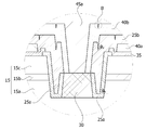
- the first electrode 30a is electrically connected to the first semiconductor layer 15a through a groove 20 formed by selectively removing the first semiconductor layer 15a, the active layer 15b, and the second semiconductor layer 15c. Can be.
- the first semiconductor layer 15a is exposed at the bottom surface 20a of the groove 20, and the first semiconductor layer 15a, the active layer 15b, and the second semiconductor layer 15 are exposed at the side surface 20b of the groove 20. 15c) may be exposed.
- a general light emitting device must secure a gap d between the first electrode 3 and the insulating pattern 1a.
- the first electrode 3 may be insulated from the insulating pattern 2 due to the process margin of the first electrode 3. Can be completely covered. One end of the first electrode 3 may extend to the second semiconductor layer 1c.
- the first electrode 30a is disposed on the bottom surface 20a of the groove 20, the first insulating pattern 25a is the side surface of the groove 20 Since the substrate 20b is disposed to overlap the first electrode 30a, only a process margin of the first electrode 30a may be considered. That is, compared with the related art, the width W1 of the first electrode 30a is wider, and the contact area of the first semiconductor layer 15a may increase.
- One end of the first insulating pattern 25a of the embodiment may extend to a part of the upper surface of the first electrode 30a. That is, since the first insulating pattern 25a completely surrounds the side surface of the first electrode 30a, the first insulating pattern 25a and the first electrode 30a are spaced apart from each other and the first semiconductor layer 15a is spaced apart from each other. This can be prevented from being exposed.
- the transparent electrode layer 35 is properly formed by forming the edge of the transparent electrode layer 35 so as to overlap the first insulating pattern 25a.
- the third gap d3 When the third gap d3 is too wide, the first insulating pattern 25a and the second reflective layer 40b are adjacent to each other, and the material of the second reflective layer 40b is formed along the first insulating pattern 25a. May enter the layer 15a.
- the third gap d3 may be an overlapping gap between the transparent electrode layer 35 and the first insulating pattern 25a.
- the transparent electrode layer 35 may not completely cover the second semiconductor layer 15c due to the process margin, and thus the second semiconductor layer 15c may be exposed. Therefore, the third interval d3 may be 2 ⁇ m to 5 ⁇ m.
- the second reflective layer 40b may be disposed to surround only the entire surface of the light emitting structure 15 while exposing only a part of the first electrode 30a and the first reflective layer 40a.
- the second reflective layer 40b may be formed of a material that performs both an insulating function and a reflective function.
- the second reflecting layer 40b may include a distributed Bragg reflector (DBR), but is not limited thereto.
- DBR distributed Bragg reflector
- One end of the second reflective layer 40a may extend to a portion of the upper surface of the first electrode 30a. This may be for the second reflective layer 40a to completely surround the edge of the first insulating pattern 25a.
- the light emitted from the active layer 15b proceeds to the upper portion of the light emitting structure 15 through the first insulating pattern 25a to emit light. This can be degraded. Therefore, in the light emitting device according to the embodiment of the present invention, one end of the second reflective layer 40b extends to a part of the upper surface of the first electrode 30a so as to completely surround the end of the first insulating pattern 25a.
- the first and second reflective layers 40a and 40b are disposed on the light emitting structure 15 to efficiently reflect the light generated from the active layer 15b toward the substrate 10. You can.
- the second electrode 30b may be disposed on the first reflective layer 40a exposed by the second reflective layer 40b.
- the second electrode 30b may be made of Ag, Ni, Al, Rh, Pd, Ir, Ru, Mg, Zn, Pt, Au, Hf, Ti, Cr, Cu, and optional combinations thereof. Do not.
- first bonding pad 45a is connected to the first electrode 30a exposed by the second reflective layer 40b, and the second bonding pad 45b is exposed by the second reflective layer 40b. It may be connected to the electrode 30b.
- FIG. 4A is a cross-sectional view of II ′ of another embodiment of FIG. 1, and FIG. 4B is an enlarged view of region A of FIG. 4A.
- the upper surface of the second reflective layer 40b is not flat and a bent portion is formed between the side surface 20b of the groove 20 and the edge of the first electrode 30a. Can be.
- the thickness of the second reflective layer 40b is not uniform due to the bent portion, which may cause a problem in that the second reflective layer 40b is not partially formed.
- the second insulating pattern 25b is disposed between the first insulating pattern 25a and the second reflective layer 40b as in the embodiment of the present invention
- the second insulating pattern 25b is the second reflective layer 40b.
- the bending degree of the B region of the second insulating pattern 25b has a sufficient thickness
- the upper surface of the second insulating pattern 25b is flat and the step coverage of the light emitting device can be improved.
- the second insulating pattern 25b may reduce variation in the coefficient of thermal expansion (CTE) of the second reflective layer 40b, the light emitting structure 15, and the first insulating pattern 25a. In addition, the second insulating pattern 25b may prevent the surface of the second reflective layer 40b from lifting or cracking due to the difference in thermal expansion coefficient.
- CTE coefficient of thermal expansion
- the second insulating pattern 25b may include an inorganic insulating material having an insulating property such as SiNX, SiOX, or the like.
- an organic insulating material such as benzocyclobuten (BCB) may be included, and the first insulating pattern 25a is not limited thereto.
- the first insulating pattern 25a and the second insulating pattern 25b are inclined along the side of the groove in a spaced area between the edge of the first electrode 30a and the edge of the bottom surface 20a of the groove 20. It can be formed into a binary structure.
- the second insulating pattern 25b and the first inclination angle ⁇ 1 of the interface between the first insulating pattern 25a and the second insulating pattern 25b are inclined along the side surface 20b of the groove 20.
- the second inclination angle ⁇ 2 of the interface of the second reflective layer 40b may be smaller.
- the first inclination angle ⁇ 1 may be 65 ° to 70 °
- the second inclination angle ⁇ 2 may be 45 ° to 60 °.
- the second inclination angle ⁇ 2 may become smaller as the thickness of the second insulating pattern 25b becomes thicker.
- the edge of the second insulating pattern 25b when the edge of the second insulating pattern 25b completely covers the edge of the first insulating pattern 25a, the exposed surface of the upper surface of the first electrode 30a may be reduced by the second insulating pattern 25b. Can be. Therefore, it is preferable that the edge of the second insulating pattern 25b coincides with the edge of the first insulating pattern 25a or exposes the edge of the first insulating pattern 25a. In the drawing, the edges of the second insulation patterns 25b coincide with the edges of the first insulation patterns 25a.
- the second reflective layer 40a may be formed to prevent the light emitted from the active layer 15b from traveling toward the first and second bonding pads 45a and 45b through the side surface 20b of the groove 20. It may be formed to completely surround the side (20b) of 20). In the drawing, the second reflective layer 40b shows the structure completely surrounding the edges of the first and second insulating patterns 25a and 25b.
- the light emitting device may increase the connection area between the first electrode 30a and the first semiconductor layer 15a without additionally removing the active layer 15b. Accordingly, the driving voltage may be improved and current spreading of the light emitting structure 15 may be facilitated.
- the second insulating pattern 25b is disposed between the first insulating pattern 25a and the second reflecting layer 40b, and is disposed between the side surface 20b of the groove 20 and the edge of the first electrode 30a. The bending degree of the second reflective layer 40b may be compensated for.
- the light emitting device according to the embodiment of the present invention as described above may further include an optical member such as a light guide plate, a prism sheet, and a diffusion sheet to function as a backlight unit.
- the light emitting device of the embodiment may be further applied to a display device, a lighting device, and a pointing device.
- the display device may include a bottom cover, a reflector, a light emitting module, a light guide plate, an optical sheet, a display panel, an image signal output circuit, and a color filter.
- the bottom cover, the reflector, the light emitting module, the light guide plate, and the optical sheet may form a backlight unit.
Landscapes
- Led Devices (AREA)
Priority Applications (3)
| Application Number | Priority Date | Filing Date | Title |
|---|---|---|---|
| CN201680077003.2A CN108431970B (zh) | 2015-12-28 | 2016-12-26 | 发光元件 |
| US16/066,511 US20190013441A1 (en) | 2015-12-28 | 2016-12-26 | Light-emitting element |
| JP2018553035A JP6968095B2 (ja) | 2015-12-28 | 2016-12-26 | 発光素子 |
Applications Claiming Priority (2)
| Application Number | Priority Date | Filing Date | Title |
|---|---|---|---|
| KR10-2015-0187457 | 2015-12-28 | ||
| KR1020150187457A KR102509144B1 (ko) | 2015-12-28 | 2015-12-28 | 발광 소자 |
Publications (1)
| Publication Number | Publication Date |
|---|---|
| WO2017116094A1 true WO2017116094A1 (ko) | 2017-07-06 |
Family
ID=59225381
Family Applications (1)
| Application Number | Title | Priority Date | Filing Date |
|---|---|---|---|
| PCT/KR2016/015253 Ceased WO2017116094A1 (ko) | 2015-12-28 | 2016-12-26 | 발광 소자 |
Country Status (5)
| Country | Link |
|---|---|
| US (1) | US20190013441A1 (enExample) |
| JP (1) | JP6968095B2 (enExample) |
| KR (1) | KR102509144B1 (enExample) |
| CN (1) | CN108431970B (enExample) |
| WO (1) | WO2017116094A1 (enExample) |
Cited By (1)
| Publication number | Priority date | Publication date | Assignee | Title |
|---|---|---|---|---|
| US20210167252A1 (en) * | 2018-07-04 | 2021-06-03 | Lg Innotek Co., Ltd. | Semiconductor device and manufacturing method therefor |
Families Citing this family (3)
| Publication number | Priority date | Publication date | Assignee | Title |
|---|---|---|---|---|
| KR102410809B1 (ko) * | 2017-08-25 | 2022-06-20 | 쑤저우 레킨 세미컨덕터 컴퍼니 리미티드 | 반도체 소자 |
| CN112470297B (zh) * | 2019-06-06 | 2022-09-06 | 新唐科技日本株式会社 | 半导体发光元件以及半导体发光装置 |
| CN110931619A (zh) * | 2019-11-20 | 2020-03-27 | 厦门士兰明镓化合物半导体有限公司 | 倒装led芯片及其制造方法 |
Citations (5)
| Publication number | Priority date | Publication date | Assignee | Title |
|---|---|---|---|---|
| JP2012069909A (ja) * | 2010-08-27 | 2012-04-05 | Toyoda Gosei Co Ltd | 発光素子 |
| JP2014096539A (ja) * | 2012-11-12 | 2014-05-22 | Tokuyama Corp | 紫外発光素子、および発光構造体 |
| KR20140103397A (ko) * | 2013-02-15 | 2014-08-27 | 삼성전자주식회사 | 반도체 발광 소자 |
| KR20150044180A (ko) * | 2013-10-16 | 2015-04-24 | 주식회사 세미콘라이트 | 반도체 발광소자 |
| KR20150062179A (ko) * | 2013-11-28 | 2015-06-08 | 일진엘이디(주) | 확장된 반사층을 가진 발광 다이오드 |
Family Cites Families (10)
| Publication number | Priority date | Publication date | Assignee | Title |
|---|---|---|---|---|
| JP5012187B2 (ja) | 2007-05-09 | 2012-08-29 | 豊田合成株式会社 | 発光装置 |
| JP5305790B2 (ja) * | 2008-08-28 | 2013-10-02 | 株式会社東芝 | 半導体発光素子 |
| JP5021693B2 (ja) * | 2009-04-14 | 2012-09-12 | スタンレー電気株式会社 | 半導体発光素子 |
| KR101142965B1 (ko) * | 2010-09-24 | 2012-05-08 | 서울반도체 주식회사 | 웨이퍼 레벨 발광 다이오드 패키지 및 그것을 제조하는 방법 |
| JP2013021175A (ja) * | 2011-07-12 | 2013-01-31 | Toshiba Corp | 半導体発光素子 |
| KR101901850B1 (ko) * | 2012-01-05 | 2018-09-27 | 엘지이노텍 주식회사 | 발광 소자, 발광 소자 패키지 및 발광 모듈 |
| KR101974153B1 (ko) * | 2012-06-12 | 2019-04-30 | 엘지이노텍 주식회사 | 발광 소자 및 이를 포함하는 조명 시스템 |
| EP2755245A3 (en) * | 2013-01-14 | 2016-05-04 | LG Innotek Co., Ltd. | Light emitting device |
| KR20150039518A (ko) * | 2013-10-02 | 2015-04-10 | 엘지이노텍 주식회사 | 발광소자 |
| JP6323176B2 (ja) * | 2014-05-30 | 2018-05-16 | 日亜化学工業株式会社 | 発光装置の製造方法 |
-
2015
- 2015-12-28 KR KR1020150187457A patent/KR102509144B1/ko active Active
-
2016
- 2016-12-26 WO PCT/KR2016/015253 patent/WO2017116094A1/ko not_active Ceased
- 2016-12-26 CN CN201680077003.2A patent/CN108431970B/zh active Active
- 2016-12-26 US US16/066,511 patent/US20190013441A1/en not_active Abandoned
- 2016-12-26 JP JP2018553035A patent/JP6968095B2/ja active Active
Patent Citations (5)
| Publication number | Priority date | Publication date | Assignee | Title |
|---|---|---|---|---|
| JP2012069909A (ja) * | 2010-08-27 | 2012-04-05 | Toyoda Gosei Co Ltd | 発光素子 |
| JP2014096539A (ja) * | 2012-11-12 | 2014-05-22 | Tokuyama Corp | 紫外発光素子、および発光構造体 |
| KR20140103397A (ko) * | 2013-02-15 | 2014-08-27 | 삼성전자주식회사 | 반도체 발광 소자 |
| KR20150044180A (ko) * | 2013-10-16 | 2015-04-24 | 주식회사 세미콘라이트 | 반도체 발광소자 |
| KR20150062179A (ko) * | 2013-11-28 | 2015-06-08 | 일진엘이디(주) | 확장된 반사층을 가진 발광 다이오드 |
Cited By (1)
| Publication number | Priority date | Publication date | Assignee | Title |
|---|---|---|---|---|
| US20210167252A1 (en) * | 2018-07-04 | 2021-06-03 | Lg Innotek Co., Ltd. | Semiconductor device and manufacturing method therefor |
Also Published As
| Publication number | Publication date |
|---|---|
| US20190013441A1 (en) | 2019-01-10 |
| CN108431970B (zh) | 2022-02-15 |
| KR20170077513A (ko) | 2017-07-06 |
| JP2019503087A (ja) | 2019-01-31 |
| KR102509144B1 (ko) | 2023-03-13 |
| JP6968095B2 (ja) | 2021-11-17 |
| CN108431970A (zh) | 2018-08-21 |
Similar Documents
| Publication | Publication Date | Title |
|---|---|---|
| KR102357188B1 (ko) | 발광 소자 | |
| EP2362449A2 (en) | Electrode structure for a light emitting device and corresponding light emitting device package | |
| WO2011126248A2 (en) | Light emitting diode and method of fabricating the same | |
| WO2017057978A1 (ko) | 발광소자 | |
| WO2009154383A2 (ko) | 반도체 발광소자 | |
| WO2016111454A1 (ko) | 발광 소자 패키지 및 이를 포함하는 발광 장치 | |
| WO2015190722A1 (ko) | 발광 소자 및 조명 장치 | |
| WO2009131319A2 (ko) | 반도체 발광소자 | |
| WO2016153213A1 (ko) | 발광 소자 패키지 및 조명 장치 | |
| WO2010095781A1 (ko) | 발광소자 및 그 제조방법 | |
| WO2018080224A1 (ko) | 반도체 소자 패키지 | |
| WO2009131335A2 (ko) | 반도체 발광소자 | |
| WO2009145501A2 (ko) | 발광 소자 및 그 제조방법 | |
| CN102222741A (zh) | 发光器件和发光器件封装 | |
| WO2016126053A1 (ko) | 발광 장치 | |
| WO2017116094A1 (ko) | 발광 소자 | |
| WO2017014580A1 (ko) | 발광 소자 패키지 | |
| WO2013137554A1 (ko) | 발광 소자 및 그 제조 방법 | |
| WO2013141421A1 (ko) | 수평형 파워 led 소자 및 그 제조방법 | |
| WO2016186330A1 (ko) | 발광 소자 | |
| WO2015190735A1 (ko) | 발광소자 및 이를 구비한 발광소자 패키지 | |
| KR20170009232A (ko) | 발광 소자 패키지 및 이를 포함하는 발광 장치 | |
| WO2019045435A1 (en) | LIGHT EMITTING DIODE APPARATUS AND METHOD FOR MANUFACTURING THE SAME | |
| WO2014193109A1 (en) | Light emitting diode having plurality of light emitting elements and method of fabricating the same | |
| CN102208509A (zh) | 发光器件、用于制造发光器件的方法以及发光器件封装 |
Legal Events
| Date | Code | Title | Description |
|---|---|---|---|
| 121 | Ep: the epo has been informed by wipo that ep was designated in this application |
Ref document number: 16882046 Country of ref document: EP Kind code of ref document: A1 |
|
| ENP | Entry into the national phase |
Ref document number: 2018553035 Country of ref document: JP Kind code of ref document: A |
|
| NENP | Non-entry into the national phase |
Ref country code: DE |
|
| 122 | Ep: pct application non-entry in european phase |
Ref document number: 16882046 Country of ref document: EP Kind code of ref document: A1 |