WO2017115633A1 - 感光性樹脂組成物及び半導体デバイス製造方法 - Google Patents
感光性樹脂組成物及び半導体デバイス製造方法 Download PDFInfo
- Publication number
- WO2017115633A1 WO2017115633A1 PCT/JP2016/086611 JP2016086611W WO2017115633A1 WO 2017115633 A1 WO2017115633 A1 WO 2017115633A1 JP 2016086611 W JP2016086611 W JP 2016086611W WO 2017115633 A1 WO2017115633 A1 WO 2017115633A1
- Authority
- WO
- WIPO (PCT)
- Prior art keywords
- photosensitive resin
- ion implantation
- resin composition
- film
- substrate
- Prior art date
- Legal status (The legal status is an assumption and is not a legal conclusion. Google has not performed a legal analysis and makes no representation as to the accuracy of the status listed.)
- Ceased
Links
Images


Classifications
-
- G—PHYSICS
- G03—PHOTOGRAPHY; CINEMATOGRAPHY; ANALOGOUS TECHNIQUES USING WAVES OTHER THAN OPTICAL WAVES; ELECTROGRAPHY; HOLOGRAPHY
- G03F—PHOTOMECHANICAL PRODUCTION OF TEXTURED OR PATTERNED SURFACES, e.g. FOR PRINTING, FOR PROCESSING OF SEMICONDUCTOR DEVICES; MATERIALS THEREFOR; ORIGINALS THEREFOR; APPARATUS SPECIALLY ADAPTED THEREFOR
- G03F7/00—Photomechanical, e.g. photolithographic, production of textured or patterned surfaces, e.g. printing surfaces; Materials therefor, e.g. comprising photoresists; Apparatus specially adapted therefor
- G03F7/004—Photosensitive materials
-
- G—PHYSICS
- G03—PHOTOGRAPHY; CINEMATOGRAPHY; ANALOGOUS TECHNIQUES USING WAVES OTHER THAN OPTICAL WAVES; ELECTROGRAPHY; HOLOGRAPHY
- G03F—PHOTOMECHANICAL PRODUCTION OF TEXTURED OR PATTERNED SURFACES, e.g. FOR PRINTING, FOR PROCESSING OF SEMICONDUCTOR DEVICES; MATERIALS THEREFOR; ORIGINALS THEREFOR; APPARATUS SPECIALLY ADAPTED THEREFOR
- G03F7/00—Photomechanical, e.g. photolithographic, production of textured or patterned surfaces, e.g. printing surfaces; Materials therefor, e.g. comprising photoresists; Apparatus specially adapted therefor
- G03F7/004—Photosensitive materials
- G03F7/0047—Photosensitive materials characterised by additives for obtaining a metallic or ceramic pattern, e.g. by firing
-
- G—PHYSICS
- G03—PHOTOGRAPHY; CINEMATOGRAPHY; ANALOGOUS TECHNIQUES USING WAVES OTHER THAN OPTICAL WAVES; ELECTROGRAPHY; HOLOGRAPHY
- G03F—PHOTOMECHANICAL PRODUCTION OF TEXTURED OR PATTERNED SURFACES, e.g. FOR PRINTING, FOR PROCESSING OF SEMICONDUCTOR DEVICES; MATERIALS THEREFOR; ORIGINALS THEREFOR; APPARATUS SPECIALLY ADAPTED THEREFOR
- G03F7/00—Photomechanical, e.g. photolithographic, production of textured or patterned surfaces, e.g. printing surfaces; Materials therefor, e.g. comprising photoresists; Apparatus specially adapted therefor
- G03F7/004—Photosensitive materials
- G03F7/075—Silicon-containing compounds
-
- G—PHYSICS
- G03—PHOTOGRAPHY; CINEMATOGRAPHY; ANALOGOUS TECHNIQUES USING WAVES OTHER THAN OPTICAL WAVES; ELECTROGRAPHY; HOLOGRAPHY
- G03F—PHOTOMECHANICAL PRODUCTION OF TEXTURED OR PATTERNED SURFACES, e.g. FOR PRINTING, FOR PROCESSING OF SEMICONDUCTOR DEVICES; MATERIALS THEREFOR; ORIGINALS THEREFOR; APPARATUS SPECIALLY ADAPTED THEREFOR
- G03F7/00—Photomechanical, e.g. photolithographic, production of textured or patterned surfaces, e.g. printing surfaces; Materials therefor, e.g. comprising photoresists; Apparatus specially adapted therefor
- G03F7/004—Photosensitive materials
- G03F7/09—Photosensitive materials characterised by structural details, e.g. supports, auxiliary layers
-
- G—PHYSICS
- G03—PHOTOGRAPHY; CINEMATOGRAPHY; ANALOGOUS TECHNIQUES USING WAVES OTHER THAN OPTICAL WAVES; ELECTROGRAPHY; HOLOGRAPHY
- G03F—PHOTOMECHANICAL PRODUCTION OF TEXTURED OR PATTERNED SURFACES, e.g. FOR PRINTING, FOR PROCESSING OF SEMICONDUCTOR DEVICES; MATERIALS THEREFOR; ORIGINALS THEREFOR; APPARATUS SPECIALLY ADAPTED THEREFOR
- G03F7/00—Photomechanical, e.g. photolithographic, production of textured or patterned surfaces, e.g. printing surfaces; Materials therefor, e.g. comprising photoresists; Apparatus specially adapted therefor
- G03F7/20—Exposure; Apparatus therefor
-
- G—PHYSICS
- G03—PHOTOGRAPHY; CINEMATOGRAPHY; ANALOGOUS TECHNIQUES USING WAVES OTHER THAN OPTICAL WAVES; ELECTROGRAPHY; HOLOGRAPHY
- G03F—PHOTOMECHANICAL PRODUCTION OF TEXTURED OR PATTERNED SURFACES, e.g. FOR PRINTING, FOR PROCESSING OF SEMICONDUCTOR DEVICES; MATERIALS THEREFOR; ORIGINALS THEREFOR; APPARATUS SPECIALLY ADAPTED THEREFOR
- G03F7/00—Photomechanical, e.g. photolithographic, production of textured or patterned surfaces, e.g. printing surfaces; Materials therefor, e.g. comprising photoresists; Apparatus specially adapted therefor
- G03F7/26—Processing photosensitive materials; Apparatus therefor
- G03F7/40—Treatment after imagewise removal, e.g. baking
-
- H—ELECTRICITY
- H10—SEMICONDUCTOR DEVICES; ELECTRIC SOLID-STATE DEVICES NOT OTHERWISE PROVIDED FOR
- H10P—GENERIC PROCESSES OR APPARATUS FOR THE MANUFACTURE OR TREATMENT OF DEVICES COVERED BY CLASS H10
- H10P14/00—Formation of materials, e.g. in the shape of layers or pillars
- H10P14/20—Formation of materials, e.g. in the shape of layers or pillars of semiconductor materials
- H10P14/34—Deposited materials, e.g. layers
- H10P14/3402—Deposited materials, e.g. layers characterised by the chemical composition
- H10P14/3404—Deposited materials, e.g. layers characterised by the chemical composition being Group IVA materials
- H10P14/3408—Silicon carbide
-
- H—ELECTRICITY
- H10—SEMICONDUCTOR DEVICES; ELECTRIC SOLID-STATE DEVICES NOT OTHERWISE PROVIDED FOR
- H10P—GENERIC PROCESSES OR APPARATUS FOR THE MANUFACTURE OR TREATMENT OF DEVICES COVERED BY CLASS H10
- H10P30/00—Ion implantation into wafers, substrates or parts of devices
- H10P30/20—Ion implantation into wafers, substrates or parts of devices into semiconductor materials, e.g. for doping
-
- H—ELECTRICITY
- H10—SEMICONDUCTOR DEVICES; ELECTRIC SOLID-STATE DEVICES NOT OTHERWISE PROVIDED FOR
- H10P—GENERIC PROCESSES OR APPARATUS FOR THE MANUFACTURE OR TREATMENT OF DEVICES COVERED BY CLASS H10
- H10P30/00—Ion implantation into wafers, substrates or parts of devices
- H10P30/20—Ion implantation into wafers, substrates or parts of devices into semiconductor materials, e.g. for doping
- H10P30/22—Ion implantation into wafers, substrates or parts of devices into semiconductor materials, e.g. for doping using masks
Definitions
- the present invention relates to a photosensitive resin composition and a semiconductor device manufacturing method using the photosensitive resin composition.
- Si semiconductor
- SiC which is a semiconductor material
- the system can be miniaturized by improving the performance of the power semiconductor device, reducing the loss, and simplifying the device cooling mechanism, which is promising as a next-generation power semiconductor material.
- SiC power device In order to manufacture a SiC power device, it is necessary to implant ions into a desired portion in SiC and dope carriers. In ion doping of SiC, since the diffusion coefficient of SiC dopant is small and it is difficult to apply a thermal diffusion method, a doping method by ion implantation is widely used.
- a high temperature ion implantation method in which the substrate is maintained at a high temperature of 200 ° C. or higher in the ion implantation step to SiC, thereby recovering the crystallinity of the substrate simultaneously with the ion implantation.
- a photoresist material used for ion implantation at room temperature for example, ion implantation into silicon, for example, a chemically amplified photoresist, is used as an ion implantation mask layer. Cannot be used.
- an inorganic film such as SiO 2 having sufficient heat resistance at the substrate temperature in the ion implantation step for example, chemical vapor deposition (CVD) (Chemical Vapor Transport ( It has been proposed to use an inorganic film such as SiO 2 deposited by CVD)) (for example, Patent Document 1).
- a dry process using a photoresist as a mask such as a wet etching method or a reactive ion etching method (RIE), is used.
- RIE reactive ion etching method
- an SiC substrate (2) having an SiC epitaxial film (1) is provided (FIG. 2 (a)), and an SiO 2 film (3) is deposited on the SiC epitaxial film (1) by a CVD method or the like. (FIG. 2 (b)).
- a photosensitive resist (4) is formed on the SiO 2 film (3) (FIG. 2C).
- patterning exposure and development which are normal photolithography processes, are performed to form a photosensitive resist pattern (FIG. 2D).
- the SiO 2 film is removed by hydrofluoric acid or the like to obtain a desired SiO 2 film pattern having a mask pattern opening (12) (FIG. 2E).
- the photosensitive resist is removed by O 2 ashing (FIG. 2F).
- ion implantation is performed at a high temperature of 200 ° C. or higher by using a dopant ion beam (7) to form an ion implantation region (6) (FIG. 2 (g)), and hydrofluoric acid or the like is used.
- the SiO 2 film is peeled off by a wet process (FIG. 2 (h)).
- This ion implantation process has many steps, is complicated, and is a high-cost process. Therefore, simplification of the process is required.
- Patent Document 2 a method of performing ion implantation at room temperature using a chemically amplified photoresist as an ion implantation mask has been proposed (for example, Patent Document 2).
- an insulating ion implantation mask is made of a conductive antistatic film such as a metal film or a doped semiconductor film.
- a technique using a method of covering in advance has been proposed (for example, Patent Document 4).
- Patent Document 5 a method of using a metal thin film such as titanium or molybdenum having a high density and high ion shielding performance as an ion implantation mask has been proposed (for example, Patent Document 5). ).
- Patent Document 6 As a method for omitting the process of forming the ion implantation mask layer, a process using a siloxane-containing photoresist is known (for example, Patent Document 6).
- Japanese Patent Application Laid-Open No. H10-228561 describes a method of using an SiO 2 film grown by a CVD method as an ion implantation mask.
- the SiO 2 film is excellent in heat resistance, ion implantation at a high temperature is possible.
- a complicated process is required for patterning the SiO 2 film, and the cost is high.
- the SiO 2 film that is an ion implantation mask does not have conductivity, there is a problem that causes a charging problem in a high-density ion implantation process.
- Patent Document 2 describes a technique of using a chemically amplified photoresist as an ion implantation mask. This technique is low in cost because the process is simple, but has a problem that the high temperature ion implantation process cannot be applied because the heat resistance of the chemically amplified photoresist is low. In addition, as described above, since the chemically amplified photoresist does not have conductivity, there is a problem that causes a charging problem in a high-density ion implantation process.
- Patent Document 3 describes a technique for solving the charging problem using an ion shower. This method has a problem of high cost because it is necessary to install an ion shower device in the semiconductor device manufacturing apparatus. In addition, it is difficult to control the amount of ion shower supplied, and it is difficult to neutralize the charge generated on the surface of the base material without excess and deficiency and completely solve the problem of charging.
- Patent Document 4 describes a method of covering an insulating ion implantation mask with a conductive antistatic film such as a metal film or a doped semiconductor film in advance when performing ion implantation. This method requires a complicated process for patterning the conductive antistatic film, and is expensive. Further, when a metal is used as an ion implantation mask or when a metal is used as a conductive film, the performance and yield of the semiconductor device may be reduced due to the mixing of metal impurities into the semiconductor substrate.
- Patent Document 5 describes a technique of using a metal thin film such as titanium or molybdenum as an ion implantation mask.
- a metal thin film such as titanium or molybdenum
- ion implantation can be performed at a high temperature without causing a charging problem.
- a metal thin film such as titanium or molybdenum
- a complicated process is required and the cost is high.
- a metal is used as an ion implantation mask, there is a possibility that the performance and yield of the semiconductor device are reduced due to the mixing of metal impurities into the semiconductor substrate.
- Patent Document 6 describes a method of obtaining a polysiloxane fired product pattern on a base material by patterning the photosensitive resin composition containing polysiloxane on the base material and thermally firing it. Although this method can form an ion implantation mask pattern having a heat resistance up to 1000 ° C. on the substrate, the polysiloxane fired product does not have conductivity, so there is a problem of charging during ion implantation. Can not be solved.
- the present invention has been made in view of the background as described above, has high-temperature heat resistance and conductivity, has no fear of causing metal impurities to the semiconductor substrate, allows pattern formation, and is low.
- a photosensitive resin composition that can be applied to a high-temperature ion implantation process at low cost.
- a photosensitive resin composition containing a photosensitive resin and particles of a conductive material and / or a semiconductor material.
- the particles are metal, metalloid, or a combination thereof.
- the particles are silicon particles.
- the silicon particles contain at least one element selected from group 13 and group 15 elements as a dopant.
- the silicon particles contain boron or phosphorus as a dopant.
- ⁇ 6> The composition according to ⁇ 4> or ⁇ 5>, wherein the concentration of the dopant in the silicon particles is 10 18 atoms / cm 3 or more.
- ⁇ 7> The composition according to any one of ⁇ 3> to ⁇ 6>, wherein the metal impurity content is 100 ppb or less for each metal element.
- ⁇ 8> The composition according to any one of ⁇ 1> to ⁇ 7>, wherein the particles have an average particle diameter of 1 to 500 nm.
- ⁇ 9> The composition according to ⁇ 8>, wherein the particles have an average particle diameter of 1 to 100 nm.
- the sheet resistance of the mask layer is 10 12.
- ⁇ 12> a step of forming a film pattern of the photosensitive resin composition according to any one of ⁇ 1> to ⁇ 11> above on a semiconductor layer or a substrate; Baking the pattern of the film of the photosensitive resin composition to form a mask for ion implantation; A step of implanting ions into the semiconductor layer or substrate through a pattern opening of the ion implantation mask; A method for manufacturing a semiconductor device, comprising a step of removing the ion implantation mask.
- ⁇ 13> The photosensitive resin composition film according to any one of ⁇ 1> to ⁇ 11> above, wherein the step of forming a pattern of the photosensitive resin composition film on the semiconductor layer or the substrate is performed.
- the high-temperature ion implantation process can save a process as compared with the conventional process, and can provide a low-cost manufacturing process.
- an antistatic device or an antistatic process on a semiconductor device which has been necessary for antistatic in the conventional ion implantation process, can be omitted. Process can be provided. Therefore, according to the manufacturing method of the present invention, it is possible to provide a low-cost power semiconductor manufacturing process with higher productivity and yield than the conventional method.
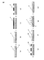
- FIG. 1 is a schematic diagram of an ion implantation process in the present invention.
- FIG. 2 is a schematic view of a conventional ion implantation process.
- FIG. 3 is a diagram showing the Al concentration distribution in the depth direction obtained by SIMS measurement in FIG.
- the photoreceptor resin composition of the present invention contains a photosensitive resin and particles of a conductive material and / or a semiconductor material.
- photosensitive resin used in the photosensitive resin composition of the present invention those having negative or positive photosensitivity can be arbitrarily selected, and in particular, the photosensitive resin used in the formation of an ion implantation mask. Can be used.
- the photosensitive resin composition of this invention can be used in order to obtain the mask used in an ion implantation process.
- the conductive material and / or the semiconductor material constituting the particles used in the present invention are formed by forming a mask for ion implantation using the photosensitive resin composition of the present invention, and when performing ion implantation, the semiconductor layer or The mask can be selected such that the mask has sufficient conductivity to suppress charging (charge-up) that occurs in the substrate and the ion implantation mask.
- a single type of particle may be used, or two or more types of particles may be used in combination.
- the conductive material and / or semiconductor material for example, 1 ⁇ 10 12 ⁇ m or less, 1 ⁇ 10 9 ⁇ m or less, 1 ⁇ 10 6 ⁇ m or less, 1 ⁇ 10 3 ⁇ m or less, 1 ⁇ 10 3 ⁇ m or less, 1 ⁇ m or less, 1 A material having a resistivity of ⁇ 10 ⁇ 3 ⁇ m or less or 1 ⁇ 10 ⁇ 6 ⁇ m or less can be selected.
- this conductive material and / or semiconductor material is preferably 1 ⁇ 10 3 ⁇ m or less, more preferably A material having a resistivity of preferably 1 ⁇ m or less, more preferably 1 ⁇ 10 ⁇ 3 ⁇ m or less, and particularly preferably 1 ⁇ 10 ⁇ 6 ⁇ m or less can be selected.
- the conductive material and / or the semiconductor material can be obtained when the photosensitive resin composition film is baked at 800 ° C. for 1 hour in the atmosphere to obtain a mask layer having a thickness of 0.5 ⁇ m.
- the sheet resistance of the layer can also be selected to be 10 12 ⁇ / ⁇ or less, 10 11 ⁇ / ⁇ or less, or 10 10 ⁇ / ⁇ or less.
- the particles used in the present invention are preferably particles of a material having a melting point exceeding the temperature of the semiconductor layer or the substrate in the ion implantation step.
- particles of a material having a melting point of 400 ° C. or higher, 600 ° C. or higher, 800 ° C. or higher, 1000 ° C. or higher, 1200 ° C. or higher, or 1500 ° C. or higher can be used as the particles used in the present invention.
- the average primary particle size of the particles used in the present invention can be 500 nm or less, 200 nm or less, 100 nm or less, 50 nm or less, 20 nm or less, or 5 nm or less.
- the average primary particle size of the particles used in the present invention can be 1 nm or more, 3 nm or more, 5 nm or more, 10 nm or more, or 20 nm or more.
- the average primary particle size of the particles used in the present invention is set to 200 nm or less, 100 nm or less, 50 nm or less, 20 nm or less, or 5 nm or less in order to suppress light scattering during patterning exposure and reduce pattern bleeding. It is preferable.
- the average primary particle diameter of the particles is a projected area circle equivalent diameter directly based on a photographed image by observation with a scanning electron microscope (SEM), a transmission electron microscope (TEM), or the like.
- the number average primary particle diameter can be obtained by measuring and analyzing a particle group consisting of 100 or more aggregates.
- particles of metal, metalloid, or a combination thereof may be used.
- examples of the semimetal include silicon and germanium.
- particles of the semiconductor material In the step of performing ion implantation by heating the semiconductor layer or the substrate to a high temperature, in order to prevent contamination of the semiconductor layer or the substrate by metal impurities, particles of the semiconductor material, particularly particles of the same semiconductor material as the semiconductor layer or the substrate are added. It is preferable to use it.
- the particles used in the present invention are silicon (Si), germanium (Ge), diamond (C), silicon carbide (SiC), silicon germanium (SiGe), gallium nitride (GaN), indium phosphide (InP).
- Particles of a semiconductor material such as gallium arsenide (GaAs), cadmium sulfide (CdS), zinc selenide (ZnSe), or zinc oxide (ZnO).
- the particles of this semiconductor material may be pre-doped with an impurity dopant and thereby have favorable conductivity.
- the particles of the semiconductor material may contain at least one element selected from group 13 and group 15 elements as a dopant. That is, the dopant may be p-type or n-type.
- the dopant may contain a dopant selected from the group consisting of phosphorus (P), arsenic (As), antimony (Sb), or combinations thereof, such as boron or phosphorus.
- silicon particles contain boron as a dopant
- boron provides preferable conductivity to silicon particles, while boron is difficult to move from silicon particles to a semiconductor substrate in an ion implantation process. preferable.
- the concentration of the dopant in the semiconductor particles, particularly silicon particles, may be 10 18 atoms / cm 3 or more, 10 19 atoms / cm 3 or more, or 10 20 atoms / cm 3 or more.
- the concentration of the metal impurity contained in the semiconductor particles is 100 ppb for each metal element in order to prevent the semiconductor layer or the substrate from being contaminated by metal impurities.
- semiconductor particles of 50 ppb or less, 20 ppb, or 10 ppb or less can be used.
- the “metal impurity” means a metal other than the metal constituting the semiconductor.
- the particles used in the present invention can be used at an arbitrary concentration as long as an ion implantation mask can be formed.
- the particles used in the present invention are preferably used in a proportion of 1% by weight to 90% by weight with respect to the photosensitive resin composition.
- the concentration of the particles By setting the concentration of the particles to 90% by weight or less, the photosensitive resin composition film can be patterned without a significant decrease in the photosensitivity of the photosensitive resin composition.
- an ion implantation mask having a film thickness sufficient to exhibit performance as an ion implantation mask layer is obtained by baking the photosensitive resin composition film. Can be formed.
- the particles used in the present invention are preferably particles obtained by a laser pyrolysis method.
- silicon particles obtained by the laser pyrolysis method for example, particles described in JP-T 2010-514585 can be used.
- the circularity may be 0.80 or more, 0.90 or more, 0.93 or more, 0.95 or more, 0.97 or more, 0.98 or more, or 0.99 or more.
- the circularity is measured by measuring the projected area (S) of the particle and the perimeter (l) of the particle from an image taken by observation with a scanning electron microscope (SEM), a transmission electron microscope (TEM), etc. using image processing software or the like. Then, (4 ⁇ S) / l 2 can be calculated. In this case, the circularity can be obtained as an average value of 100 or more particle groups.
- silicon particles obtained by the laser pyrolysis method it can be mentioned that the inside of the particles is in a crystalline state and the particle surface portion is in an amorphous state. This can give unique physical properties to the various articles in which the particles are used.
- silicon particles in which the inside of the particle is in a crystalline state and the particle surface portion is in an amorphous state can also be suitably used.
- the photosensitive resin composition of the present invention may further contain a solvent.
- a solvent there is no restriction
- the boiling point under atmospheric pressure of the solvent contained in the photosensitive resin composition of the present invention is preferably 110 ° C. to 250 ° C.
- a solvent having a boiling point of 110 ° C. or higher the solvent evaporates at an appropriate rate when the photosensitive resin composition film is formed, and a uniform film is obtained.
- a solvent having a boiling point of 250 ° C. or less it is possible to reduce the amount of solvent remaining in the photosensitive resin composition film after the formation of the photosensitive resin composition film. It is possible to suppress cracks and surface flatness due to the above.
- the photosensitive resin composition of the present invention may contain a binder for the purpose of binding particles in the baking step of the photosensitive resin composition to form a stable ion implantation mask.
- a binder for the purpose of binding particles in the baking step of the photosensitive resin composition to form a stable ion implantation mask.
- the binder used in the photosensitive resin composition of the present invention include a polysiloxane compound and spin-on glass.
- the inventive method for manufacturing a semiconductor device comprises the following steps: Forming a film pattern of the photosensitive resin composition of the present invention on a semiconductor layer or substrate; Baking the pattern of the film of the photosensitive resin composition to form a mask for ion implantation; A step of implanting ions into the semiconductor layer or the substrate through a pattern opening of the mask for ion implantation, and a step of removing the mask for ion implantation.
- the step of forming the pattern of the photosensitive resin composition film on the semiconductor layer or the substrate includes forming the photosensitive resin composition film of the present invention on the semiconductor substrate, and this photosensitive resin composition. Patterning exposure and development may be included on the object film.
- an SiC substrate (2) having an SiC epitaxial film (1) is provided, and as shown in FIG. 1 (b), a photosensitive resin composition film (11) is provided. ) Is formed on the SiC substrate by any method.
- patterning exposure is performed by patterning exposure of the photosensitive resin composition having light or the like having sensitivity to the photosensitive resin composition film, and immersing the SiC substrate having the photosensitive resin composition film in a developer.
- membrane of the photosensitive resin composition which passed through the process is removed.
- membrane of the photosensitive resin composition which has a mask pattern opening part (12) is formed on a SiC base material (2).
- the SiC base material on which the film of the photosensitive resin composition is formed is baked at a temperature at which the organic component contained in the photosensitive resin composition is decomposed, whereby ion implantation is performed.
- a mask (13) can be obtained.
- an ion implantation apparatus is used to pass through the mask pattern opening (12) of the ion implantation mask (13) with the beam (7) of dopant ions of the SiC substrate (2).
- an ion implantation region (6) is formed.
- the ion implantation process can be performed by heating the semiconductor layer or the substrate to be ion-implanted to a temperature of 200 ° C. or higher.
- the ion implantation mask (13) can be removed by means such as immersion in a dissolvable chemical solution.
- any semiconductor layer or substrate intended to diffuse the dopant can be used.
- silicon Si
- germanium Ge
- diamond C
- silicon carbide SiC
- silicon germanium SiGe
- gallium nitride GaN
- indium phosphide InP
- examples include, but are not limited to, gallium arsenide (GaAs), cadmium sulfide (CdS), zinc selenide (ZnSe), zinc oxide (ZnO), and particularly silicon carbide (SiC).
- the semiconductor layer or the substrate may be composed of a single layer or a laminate composed of two or more types of layers including one or more semiconductor layers.
- a laminate is a semiconductor laminate having an epitaxial film such as an SiC epitaxial film grown on a semiconductor single crystal substrate such as an SiC single crystal substrate for the purpose of obtaining desired semiconductor device characteristics. It may be.
- the semiconductor layer or substrate may be a semiconductor layer or substrate having an impurity dopant of 10 16 atoms / cm 3 or less, and may be pre-doped to a concentration exceeding 10 16 atoms / cm 3 with an impurity dopant.
- a metal film or a metal wiring pattern may be formed in advance on the semiconductor layer or the substrate.
- a film pattern of the photosensitive resin composition of the present invention is formed on a semiconductor layer or a substrate.
- This step may include forming a film of the photosensitive resin composition of the present invention on a semiconductor substrate, and patterning exposure and development on the film of the photosensitive resin composition.
- the film of the photosensitive resin composition of the present invention can be formed on the semiconductor substrate by any means capable of forming the film of the photosensitive resin composition on the semiconductor layer or the substrate.
- examples of such means include a spin coating method, a slit coating method, a spray coating method, or a laminating method in which a photosensitive resin composition film prepared on another substrate in advance is transferred onto a semiconductor substrate.
- any method that is not limited to these can be selected.
- the photosensitive resin composition contains a solvent
- it can be baked and the solvent removed after formation of the film of the photosensitive resin composition.
- a method for removing the solvent by heating a method capable of arbitrary heating such as an oven, a hot plate, and infrared rays can be used.
- Arbitrary thickness can be selected as the film thickness of the photosensitive resin composition film.
- the film thickness varies depending on the composition of the photosensitive resin composition, the coating conditions, the coating method, and the like.
- the coating can be performed so that the film thickness of the photosensitive resin composition is 0.1 ⁇ m to 100 ⁇ m.
- the film thickness is sufficient as a mask layer for ion implantation. Therefore, for example, in consideration of factors that affect the ion implantation penetration depth, such as the temperature of the semiconductor substrate, the ion acceleration voltage, and the dopant ion species during ion implantation, the resulting ion implantation mask has sufficient ions.
- the film thickness of the photosensitive resin composition film can be selected so that the film thickness has a stopping power.
- the photosensitive resin composition film can be subjected to patterning exposure by any method suitable for the resist.
- Exposure is to irradiate the photosensitive resin composition with active actinic radiation having photosensitivity, and examples thereof include irradiation with visible light, ultraviolet rays, electron beams, and X-rays. From the viewpoint of being a commonly used light source, for example, it is preferable to use an ultra-high pressure mercury lamp light source capable of irradiating visible light or ultraviolet light. J-line (wavelength 313 nm), i-line (wavelength 365 nm) H-line (wavelength 405 nm) or g-line (wavelength 436 nm).
- the following pre-development baking may be performed as necessary.
- pre-development baking it is possible to expect effects such as improvement in resolution during development and increase in the allowable range of development conditions.
- the baking temperature is preferably 50 to 180 ° C, more preferably 60 to 150 ° C.
- the baking time is preferably 10 seconds to several hours. Within the above range, there are advantages that the reaction proceeds satisfactorily and the development time can be shortened.
- the pattern of the photosensitive resin composition can be obtained by development after patterning exposure.
- a film of a photosensitive resin composition after patterning exposure is immersed in a developing solution, if the photosensitive resin composition has negative photosensitivity, the non-exposed portion is removed, and the photosensitive resin composition In the case of having positive-type photosensitivity, the exposed portion is removed, and the film of the photosensitive resin composition can be patterned.
- any developer can be selected according to the composition of the photosensitive resin composition.
- a developer exhibiting alkaline liquidity can be preferably used.
- tetramethylammonium hydroxide, potassium hydroxide, and sodium hydroxide can be preferably used.
- the developer may contain a solvent in order to improve the dissolution of the patterning site and the dispersibility of the conductive particles.
- a solvent in order to improve the dissolution of the patterning site and the dispersibility of the conductive particles.
- isopropyl alcohol, acetone, propylene glycol 1-monomethyl ether 2-acetate and the like can be preferably used.
- the developer may contain a surfactant in order to improve the dissolution of the patterning site and the dispersibility of the conductive particles.
- the above-described developer is directly applied to the exposed film, the developer is sprayed and emitted, the exposed film is immersed in the developer, and the exposed film is exposed. It can be performed by a method such as applying ultrasonic waves while being immersed in the developer.
- a rinse solution water can be preferably used when an alkaline aqueous solution is used as the developer. Further, rinsing may be performed by adding alcohols such as ethanol and isopropyl alcohol, esters such as propylene glycol monomethyl ether acetate, acids such as carbon dioxide, hydrochloric acid, and acetic acid to water.
- alcohols such as ethanol and isopropyl alcohol
- esters such as propylene glycol monomethyl ether acetate
- acids such as carbon dioxide, hydrochloric acid, and acetic acid
- methanol, ethanol, isopropyl alcohol, ethyl lactate, ethyl pyruvate, propylene glycol monomethyl ether acetate, methyl-3-methoxypropionate, ethyl-3- Ethoxypropionate, 2-heptanone, ethyl acetate and the like are preferably used.
- bleaching exposure may be performed without using a mask, if necessary.
- effects such as improvement in resolution after baking, control of the pattern shape after baking, and improvement in transparency after baking can be expected.
- Active actinic rays used for bleaching exposure include ultraviolet rays, visible rays, electron beams, X-rays, etc.
- mercury lamp j-ray (wavelength 313 nm), i-ray (wavelength 365 nm), h-ray (wavelength) 405 nm) or g-line (wavelength 436 nm) is preferably used.
- middle baking may be performed as necessary.
- effects such as improvement in resolution after baking and control of the pattern shape after baking can be expected.
- the baking temperature at this time is preferably 60 to 250 ° C, more preferably 70 to 220 ° C.
- the baking time is preferably 10 seconds to several hours.
- This heat treatment can be performed in an air atmosphere or an inert gas atmosphere such as nitrogen.
- this heat treatment is performed stepwise or continuously, and is performed for 5 minutes to 5 hours. For example, heat treatment is performed at 130 ° C., 200 ° C., and 350 ° C. for 30 minutes each, or the temperature is increased linearly from room temperature to 400 ° C. over 2 hours.
- ions are implanted into the semiconductor layer or the substrate through the pattern opening of the ion implantation mask.
- the ion implantation mask is preferably applied to a semiconductor device manufacturing process including ion implantation into a SiC layer or substrate having an ion implantation temperature of 200 to 1000 ° C.
- the ion implantation temperature is preferably 200 to 1000 ° C., more preferably 200 to 800 ° C., further preferably 250 to 700 ° C., and particularly preferably 300 ° C. to 500 ° C.
- the semiconductor layer or base material is a SiC layer or base material
- the ion implantation temperature is lower than 200 ° C.
- the injection layer becomes a continuous amorphous state, and good recrystallization proceeds even if high-temperature annealing is performed. Therefore, there is a concern that a low resistance layer cannot be formed.
- the ion implantation temperature is higher than 1000 ° C., thermal oxidation or step bunching of SiC occurs, and it is necessary to remove those portions after ion implantation.
- the resolution is preferably 7 ⁇ m or less, more preferably 5 ⁇ m or less, and even more preferably 3 ⁇ m or less.
- the ion implantation mask is removed after the ion implantation process.
- the removal method include, but are not limited to, a wet process using hydrofluoric acid, buffered hydrofluoric acid, hydrofluoric acid, or TMAH, a dry process such as plasma treatment, and the like.
- a wet process is preferable from the viewpoint of low cost.
- Examples 1-2 and Comparative Examples 1-3 >> In Examples 1 to 2 and Comparative Examples 1 to 3 below, a photosensitive resin composition was prepared, a coating film was formed on a SiC substrate, and then patterning exposure to ultraviolet light, development, and baking were performed. The resulting ion implantation mask was patterned. In addition, these Examples and Comparative Examples were evaluated for the possibility of patterning, the presence or absence of a pattern after thermal baking, and the presence or absence of problems due to charging during ion implantation.
- Example 1 (Preparation of boron (B) doped silicon particles) Silicon nanoparticles were produced by a laser pyrolysis (LP) method using a carbon dioxide laser using monosilane gas as a raw material. At this time, diborane (B 2 H 6 ) gas was introduced together with monosilane gas to obtain boron-doped silicon particles. The particle diameter of this particle was 20 nm.
- the doping concentration of the obtained boron-doped silicon particles was 1 ⁇ 10 21 atoms / cm 3 . Further, when the metal impurity content of the obtained boron-doped silicon particles was measured with an inductively coupled plasma mass spectrometer (ICP-MS), the Fe content was 15 ppb, the Cu content was 18 ppb, and the Ni content was 10 ppb, the Cr content was 21 ppb, the Co content was 13 ppb, the Na content was 20 ppb, and the Ca content was 10 ppb.
- ICP-MS inductively coupled plasma mass spectrometer
- a boron-doped silicon particle-containing solution was prepared by mixing 95% by weight of isopropyl alcohol and 5% by weight of silicon nanoparticles prepared by the above method.
- a photosensitive resin composition containing a silicon nanoparticle and a negative photosensitive resin by mixing a negative photoresist (CTP-100T, manufactured by Merck Performance Materials Manufacturing LLC) and the boron-doped silicon particle-containing solution. A product was prepared. At this time, a photosensitive resin composition was prepared so that boron-doped silicon nanoparticles accounted for 20% by weight of the solid content of the photosensitive resin composition after mixing.
- CTP-100T negative photoresist
- the photosensitive resin composition containing the silicon nanoparticles and the negative photosensitive resin is spin-coated at a rotation speed such that the film thickness is about 2 ⁇ m, and is heated on a hot plate at 100 ° C. to 90 ° C. By drying for 2 seconds, a photosensitive resin composition film was obtained.
- the photosensitive resin composition film was exposed to patterning by irradiating ultraviolet light through a photomask pattern using a patterning exposure machine. Patterning exposure was performed using a photomask having a 10 ⁇ m line and space as a photomask.
- the photosensitive resin composition film after patterning exposure is heated on a hot plate at 100 ° C. for 90 seconds, and then immersed in a developer (AZ-300MIF, manufactured by Merck Performance Materials Manufacturing LLC) for 60 seconds to form a pattern.
- AZ-300MIF manufactured by Merck Performance Materials Manufacturing LLC
- the pattern of the photosensitive resin composition film was baked at 800 ° C. for 1 hour in the atmosphere in an oven to form an ion implantation mask on the SiC substrate.
- the film thickness of the mask layer for ion implantation after baking was 0.5 ⁇ m.
- Ion implantation Ions were implanted into the SiC substrate through the mask pattern opening of the fired ion implantation mask under the following conditions: Ion species: Al, Energy amount: 40 keV, Injection temperature: 400 ° C Dose amount: 1 ⁇ 10 14 Ions / cm 2
- the ion implantation mask was removed by immersing the base material in a mixed solution of buffered hydrofluoric acid and concentrated sulfuric acid. Then, the depth dependence from the SiC base material surface of Al concentration was measured using the secondary ion mass spectrometry (SIMS) apparatus.
- SIMS secondary ion mass spectrometry
- FIG. 3 shows the Al concentration distribution in the depth direction obtained by SIMS measurement.
- Al ions are implanted into the surface of the SiC base material in the region that was the opening of the ion implantation mask at the time of Al ion implantation.
- Al ions are not implanted into the surface of the SiC base material in the region covered by the mask, and the mask layer for ion implantation in this example has an effect of shielding the implanted ions during ion implantation. Understood.
- a photosensitive resin composition instead of mixing a negative photoresist (CTP-100T, manufactured by Merck Performance Materials Manufacturing LLC) and the boron-doped silicon particle-containing solution, a negative photoresist (CTP-100T) is used. , Merck Performance Materials Manufacturing LLC), the above boron-doped silicon particle-containing solution, and spin-on glass (12000-T, manufactured by Tokyo Ohka Kogyo Co., Ltd.). Then, a mask layer was formed on the SiC substrate.
- CTP-100T negative photoresist
- Merck Performance Materials Manufacturing LLC Merck Performance Materials Manufacturing LLC
- spin-on glass (12000-T, manufactured by Tokyo Ohka Kogyo Co., Ltd.
- the photosensitive resin composition is such that 10% by weight is occupied by boron-doped silicon nanoparticles and 10% by weight is solid content contained in the spin-on-glass solution.
- a product was prepared.
- a photosensitive resin composition instead of mixing a negative photoresist (CTP-100T, manufactured by Merck Performance Materials Manufacturing LLC) and the boron-doped silicon particle-containing solution, a negative photoresist (CTP-100T) is used.
- SiC base material in the same manner as in Example 1, except that the SiO 2 nanoparticle dispersion solution SIRPMA30WT% -E9 (CIK Nanotech Co., Ltd.) was mixed. A mask layer was formed thereon.
- the photosensitive resin composition was prepared such that 20% by weight of the solid content of the photosensitive resin composition after mixing was occupied by the solid content contained in the SiO 2 nanoparticle dispersion solution SIRPMA30WT% -E9.
- a photosensitive resin composition instead of mixing a negative photoresist (CTP-100T, manufactured by Merck Performance Materials Manufacturing LLC) and the boron-doped silicon particle-containing solution, a negative photoresist (CTP-100T) is used. , Merck Performance Materials Manufacturing GK) and spin-on glass (12000-T, manufactured by Tokyo Ohka Kogyo Co., Ltd.), and a mask layer is formed on the SiC substrate in the same manner as in Example 1. did. Under the present circumstances, the photosensitive resin composition was prepared so that solid content contained in spin-on glass might occupy 20 weight% among solid content of the photosensitive resin composition after mixing.
- a photosensitive resin composition instead of using a negative photoresist (CTP-100T, manufactured by Merck Performance Materials Manufacturing Godo Kaisha) and a solution containing the boron-doped silicon particle-containing solution, a negative photoresist (A step of forming a mask layer on the SiC substrate was performed in the same manner as in Example 1 except that CTP-100T (manufactured by Merck Performance Materials Manufacturing LLC) was used.
- CTP-100T manufactured by Merck Performance Materials Manufacturing LLC
- the heat after patterning of the photosensitive resin composition can be obtained by mixing spin-on glass as a binder in addition to conductive silicon nanoparticles as an additive. It is understood that a residue pattern having conductivity can be formed on the substrate by firing.
- Example 3 and Comparative Example 4 >> In Example 3 and Comparative Example 4 below, a photosensitive resin composition was prepared, a coating film was formed on a substrate with a thermal silicon oxide film of 1000 nm, and thereafter patterning exposure to ultraviolet light, development, and baking were performed. Then, the mask layer was patterned. In these examples and comparative examples, the sheet resistance of the mask layer was measured.
- Example 3> instead of using the SiC substrate as the substrate, a silicon wafer with a thermally oxidized silicon film of 1000 nm was used, and except that the entire surface of the substrate was exposed to ultraviolet light during patterning exposure, the same as in Example 1, Pattern formation of the mask layer was performed. After pattern formation of the mask layer, an aluminum electrode for the purpose of measuring the resistivity of the mask layer pattern was formed on the mask layer pattern using a vacuum evaporation method through a shadow mask.
- an electrode pattern in which 1000 ⁇ m sides of a pair of rectangular electrodes having a size of 1000 ⁇ m ⁇ 200 ⁇ m are opposed to each other at an interval of 200 ⁇ m is used. It was.
- the sheet resistance of the mask layer was determined by measuring the potential drop between the aluminum electrodes when a constant current of 1 ⁇ A was applied between the deposited aluminum electrodes, and found to be 90 G ⁇ / ⁇ .
- ⁇ Comparative example 4> An ion implantation mask having a pattern on a silicon substrate in the same manner as in Example 3 except that spin-on glass (12000-T, manufactured by Tokyo Ohka Kogyo Co., Ltd.) was used instead of the boron-doped silicon particle-containing solution. After forming, the sheet resistance of this ion implantation mask was measured. According to this, a current exceeding the measurement limit of the apparatus was not measured, and the sheet resistance of the mask layer was estimated to be 2.0 ⁇ 10 8 G ⁇ / ⁇ or more.
Landscapes
- Physics & Mathematics (AREA)
- General Physics & Mathematics (AREA)
- Engineering & Computer Science (AREA)
- Chemical & Material Sciences (AREA)
- Ceramic Engineering (AREA)
- Architecture (AREA)
- Structural Engineering (AREA)
- Materials For Photolithography (AREA)
- Exposure And Positioning Against Photoresist Photosensitive Materials (AREA)
- Photosensitive Polymer And Photoresist Processing (AREA)
Abstract
高温耐熱性かつ導電性を有し、半導体基材に対して金属不純物を生じる懸念がなく、パターン形成が可能で、かつ低コストで高温のイオン注入プロセスに適用できる、感光性樹脂組成物及びそのような組成物を用いる半導体デバイスの製造方法を提供する。 本発明の感光性樹脂組成物は、感光性樹脂、並びに導電性材料及び/又は半導体材料の粒子を含有している。また、半導体デバイスを製造する本発明の方法は、本発明の感光性樹脂組成物の膜のパターン(11)を、半導体層又は基材(2)上に形成する工程、感光性樹脂組成物の膜のパターンを焼成して、イオン注入用マスク(13)を形成する工程、イオン注入用マスクのパターン開口部(12)を通して、半導体層又は基材(2)にイオンを注入する工程、及びイオン注入用マスク(13)を除去する工程を含む。
Description
本発明は、感光性樹脂組成物、及びこの感光性樹脂組成物を用いる半導体デバイス製造方法に関する。
現在のパワー半導体デバイスのほとんどは、半導体Siを用いて製造されている。Siを用いたパワー半導体デバイスにおいては、Siの材料物性に起因する性能の限界に近付いている。半導体材料であるSiCは、半導体Siを大きく上回る耐電圧特性、高飽和電子移動度、高い熱伝導度を有する。したがって、パワー半導体デバイスの性能向上、低損失化、及びデバイス冷却機構の簡略化によるシステムの小型化が可能であるため、次世代のパワー半導体材料として有望である。
SiCパワーデバイスの製造のためには、SiC中の所望の部分にイオンを注入しキャリアをドープすることが必要である。SiCへのイオンドープにおいては、SiCのドーパントの拡散係数が小さく、熱拡散法の適用は困難であるため、イオン注入によるドーピング法が広く用いられる。
SiCをイオン注入により低抵抗化する工程においては、高ドーズのイオン注入を行う必要がある。しかし室温で高濃度のイオン注入を行うと、SiCのアモルファス化が起きるため、期待するデバイス性能が得られない。また、一旦アモルファス化したSiCは、熱焼成などによっても、イオン注入前と同等の結晶性をもつ同多形の構造に復元することは困難である。
そこで、SiCへのイオン注入工程において基材を200℃以上の高温に保持することにより、イオン注入と同時に基材の結晶性を回復させる、高温イオン注入法が知られている。
上記の高温イオン注入法では、イオン注入を200℃以上の高温で行うため、イオン注入マスク層として、室温でのイオン注入、例えばシリコンに対するイオン注入で用いられるフォトレジスト材料、例えば化学増幅型フォトレジストを利用することができない。
したがって、上記の高温イオン注入法においては、イオン注入マスクとして、イオン注入工程の基材温度で十分な耐熱性を有するSiO2等の無機膜、例えば化学気相堆積法(CVD:Chemical Vapor Transport(CVD))などで堆積されたSiO2等の無機膜を用いることが提案されている(例えば特許文献1)。このような耐熱性のイオン注入マスクを半導体SiC上に予めパターニングすることにより、イオン注入マスクの開口部を通じて、半導体SiC中の所望の領域にキャリアドーピングを行うことができる。
このような耐熱性のイオン注入マスクのパターニングには、フォトレジストをマスクとして用いた、ウェットエッチング法、反応性イオエッチング法(RIE)などのドライプロセスが利用される。
上記のイオン注入マスク形成工程及びイオン注入工程の例を、図2を用いて説明する。
まず、SiCエピタキシャル膜(1)を有するSiC基材(2)を提供し(図2(a))、このSiCエピタキシャル膜(1)上に、CVD法等によりSiO2膜(3)を堆積させる(図2(b))。次に、SiO2膜(3)上に感光性レジスト(4)を製膜する(図2(c))。その後、通常のフォトリソ工程である、パターニング露光及び現像を行い、感光性レジストのパターン形成を行う(図2(d))。その後、フッ化水素酸などにより、SiO2膜の除去を行い、マスクパターン開口部(12)を有する所望のSiO2膜パターンを得る(図2(e))。次いで、O2アッシングにより感光性レジストの剥離を行う(図2(f))。その後、ドーパントイオンのビーム(7)を用いて、200℃以上の高温でイオン注入を行って、イオン注入領域(6)を形成し(図2(g))、そしてフッ化水素酸などを用いたウェットプロセスでSiO2膜を剥離する(図2(h))。
このイオン注入プロセスは工程数が多く、煩雑で高コストプロセスであるため、プロセスの簡略化が求められている。
プロセスを簡略化するために、化学増幅型フォトレジストをイオン注入マスクとして利用して、室温においてイオン注入を行う手法が提案されている(例えば特許文献2)。
特許文献1及び2でのように、イオン注入マスクなどの絶縁体膜で覆われた半導体に対して高密度イオン注入を行う場合、基材及び絶縁体膜に発生する帯電(チャージアップ)が問題となる。イオン注入工程中に基材及び絶縁体膜が帯電すると、半導体中のイオン注入がなされた領域、イオン注入マスクなどの絶縁体、及び半導体基材の間で電位差が生じ、放電現象が生じることがある。また、帯電により発生した空間電場により、注入されるイオン密度の不均一化が発生することがある。このような原因により、絶縁体膜で覆われた半導体へ高密度イオン注入を行う場合には、半導体デバイスの性能及び歩留まりの低下を招くことが知られている。この帯電現象は、特に半導体表面がSiO2をはじめとした絶縁体膜で覆われている場合に顕著である。
上記帯電の問題を解決する為に、注入イオンと逆の極性を持つ低エネルギーの2次イオンシャワーを基材表面に供給し、基材の帯電の中和を図る手法が提案されている(例えば特許文献3)。
イオンシャワーを用いた手法のほかに、上記帯電の問題を解決する手法としては、イオン注入を行う際、絶縁性のイオン注入マスクを金属膜やドープされた半導体膜などの導電性帯電防止膜で予め被覆する手法を利用する技術が提案されている(例えば特許文献4)。
また、イオン注入マスクのイオンブロッキング層としての向上を目的として、密度が大きくイオン遮蔽性能の高い、チタンやモリブデンなどの金属薄膜をイオン注入マスクとして利用する手法が提案されている(例えば特許文献5)。
なお、イオン注入マスク層形成のプロセスを省略する手法としては、シロキサンを含有するフォトレジストを用いるプロセスが公知である(例えば特許文献6)。
特許文献1は、CVD法で成長させたSiO2膜をイオン注入マスクとして利用する手法を記載している。この手法は、SiO2膜が耐熱性に優れるため、高温でのイオン注入が可能であるが、SiO2膜のパターニングに煩雑なプロセスが必要であり、高コストである。また、上記のように、イオン注入マスクであるSiO2膜は導電性を有さないため、高密度のイオン注入工程において帯電の問題を生じる課題がある。
特許文献2は、化学増幅型フォトレジストをイオン注入マスクとして利用する手法を記載している。この手法は、プロセスが簡便であるため低コストであるが、化学増幅型フォトレジストの耐熱性が低いため、高温イオン注入プロセスを適用できない課題がある。また、上記のように、化学増幅型フォトレジストは導電性を有さないため、高密度のイオン注入工程において帯電の問題を生じる課題がある。
特許文献3は、イオンシャワーを用いて帯電の問題を解決する手法を記載している。この手法は、半導体デバイス製造装置に、イオンシャワー装置の設置が必要となるため高コストである課題がある。また、イオンシャワー供給量の制御が困難であり、基材表面に生じる帯電を過不足なく中和し、帯電の課題を完全に解決することは困難である。
特許文献4は、イオン注入を行う際に、予め絶縁性のイオン注入マスクを金属膜やドープされた半導体膜などの導電性帯電防止膜で被覆する手法を記載している。この手法は、導電性帯電防止膜のパターニングに煩雑なプロセスが必要であり、高コストである。また、金属をイオン注入マスクとして用いた場合及び金属を導電膜として用いた場合には、半導体基材への金属不純物の混入により、半導体デバイスの性能及び歩留まりの低下を招く可能性がある。
特許文献5は、チタンやモリブデンなどの金属薄膜をイオン注入マスクとして利用する手法を記載している。この手法は、金属薄膜が耐熱性に優れ、かつ導電性を有するため、帯電の問題を生じることなく高温においてイオン注入が可能である。一方で、チタンやモリブデンなどの金属薄膜のパターニングを行うためには、煩雑なプロセスが必要であり、高コストである。また、金属をイオン注入マスクとして用いた場合、半導体基材への金属不純物の混入に起因して、半導体デバイスの性能及び歩留まりの低下を招く可能性がある。
特許文献6は、ポリシロキサンを含有する感光性樹脂組成物を、基材上にパターニングし熱焼成することで、ポリシロキサンの焼成物パターンを基材上に得る手法を記載している。この手法は、1000℃までの耐熱性を有するイオン注入マスクパターンを基材上に形成することが可能であるが、ポリシロキサン焼成物は導電性を有さないため、イオン注入時の帯電の問題を解決することができない。
本発明では、上述のような背景を鑑みてなされたものであり、高温耐熱性かつ導電性を有し、半導体基材に対して金属不純物を生じる懸念がなく、パターン形成が可能で、かつ低コストで高温のイオン注入プロセスに適用できる、感光性樹脂組成物を提供する。
上記の課題に対して、本件の発明者らは下記の本発明に想到した。
〈1〉感光性樹脂、並びに導電性材料及び/又は半導体材料の粒子を含有している、感光性樹脂組成物。
〈2〉前記粒子が、金属、半金属、又はそれらの組合せの粒子である、上記〈1〉項に記載の組成物。
〈3〉前記粒子が、シリコン粒子である、上記〈2〉項に記載の組成物。
〈4〉前記シリコン粒子が、13族及び15族元素のうち少なくとも一種類の元素をドーパントとして含有している、上記〈3〉項に記載の組成物。
〈5〉前記シリコン粒子が、ホウ素又はリンをドーパントとして含有している、上記〈4〉項に記載の組成物。
〈6〉前記シリコン粒子における前記ドーパントの濃度が、1018atoms/cm3以上である、上記〈4〉又は〈5〉項に記載の組成物。
〈7〉金属不純物含有量がそれぞれの金属元素について100ppb以下である、上記〈3〉~〈6〉項のいずれか一項に記載の組成物。
〈8〉前記粒子の平均粒径が1~500nmである、上記〈1〉~〈7〉項のいずれか一項に記載の組成物。
〈9〉前記粒子の平均粒径が1~100nmである、上記〈8〉項に記載の組成物。
〈10〉前記感光性樹脂組成物の膜を、大気下で800℃の焼成を1時間行って、膜厚0.5μmのマスク層を得たときに、このマスク層のシート抵抗が、1012Ω/□以下である、上記〈1〉~〈9〉項のいずれか一項に記載の組成物。
〈11〉シロキサン化合物を更に含有している、上記〈1〉~〈10〉項のいずれか一項に記載の組成物。
〈12〉上記〈1〉~〈11〉項のいずれか一項に記載の感光性樹脂組成物の膜のパターンを、半導体層又は基材上に形成する工程、
前記感光性樹脂組成物の膜のパターンを焼成して、イオン注入用マスクを形成する工程、
前記イオン注入用マスクのパターン開口部を通して、前記半導体層又は基材にイオンを注入する工程、
前記イオン注入用マスクを除去する工程
を含む、半導体デバイスの製造方法。
〈13〉前記感光性樹脂組成物の膜のパターンを半導体層又は基材上に形成する工程が、上記〈1〉~〈11〉項のいずれか一項に記載の感光性樹脂組成物の膜を半導体基材上に形成し、そして前記感光性樹脂組成物の膜にパターニング露光及び現像することを含む、上記〈12〉項に記載の方法。
〈14〉前記半導体層又は基材が、SiC層又は基材である、上記〈12〉又は〈13〉項に記載の方法。
〈15〉イオン注入工程における前記半導体層又は基材の温度が、200℃以上である、上記〈12〉~〈14〉項のいずれか一項に記載の方法。
〈2〉前記粒子が、金属、半金属、又はそれらの組合せの粒子である、上記〈1〉項に記載の組成物。
〈3〉前記粒子が、シリコン粒子である、上記〈2〉項に記載の組成物。
〈4〉前記シリコン粒子が、13族及び15族元素のうち少なくとも一種類の元素をドーパントとして含有している、上記〈3〉項に記載の組成物。
〈5〉前記シリコン粒子が、ホウ素又はリンをドーパントとして含有している、上記〈4〉項に記載の組成物。
〈6〉前記シリコン粒子における前記ドーパントの濃度が、1018atoms/cm3以上である、上記〈4〉又は〈5〉項に記載の組成物。
〈7〉金属不純物含有量がそれぞれの金属元素について100ppb以下である、上記〈3〉~〈6〉項のいずれか一項に記載の組成物。
〈8〉前記粒子の平均粒径が1~500nmである、上記〈1〉~〈7〉項のいずれか一項に記載の組成物。
〈9〉前記粒子の平均粒径が1~100nmである、上記〈8〉項に記載の組成物。
〈10〉前記感光性樹脂組成物の膜を、大気下で800℃の焼成を1時間行って、膜厚0.5μmのマスク層を得たときに、このマスク層のシート抵抗が、1012Ω/□以下である、上記〈1〉~〈9〉項のいずれか一項に記載の組成物。
〈11〉シロキサン化合物を更に含有している、上記〈1〉~〈10〉項のいずれか一項に記載の組成物。
〈12〉上記〈1〉~〈11〉項のいずれか一項に記載の感光性樹脂組成物の膜のパターンを、半導体層又は基材上に形成する工程、
前記感光性樹脂組成物の膜のパターンを焼成して、イオン注入用マスクを形成する工程、
前記イオン注入用マスクのパターン開口部を通して、前記半導体層又は基材にイオンを注入する工程、
前記イオン注入用マスクを除去する工程
を含む、半導体デバイスの製造方法。
〈13〉前記感光性樹脂組成物の膜のパターンを半導体層又は基材上に形成する工程が、上記〈1〉~〈11〉項のいずれか一項に記載の感光性樹脂組成物の膜を半導体基材上に形成し、そして前記感光性樹脂組成物の膜にパターニング露光及び現像することを含む、上記〈12〉項に記載の方法。
〈14〉前記半導体層又は基材が、SiC層又は基材である、上記〈12〉又は〈13〉項に記載の方法。
〈15〉イオン注入工程における前記半導体層又は基材の温度が、200℃以上である、上記〈12〉~〈14〉項のいずれか一項に記載の方法。
本発明の感光性樹脂組成物によれば、高温のイオン注入プロセスにおいて、従来のプロセスと比較して省プロセス化が可能であり、低コストな製造プロセスを提供することができる。また、本発明の感光性樹脂組成物によれば、従来のイオン注入プロセスで帯電防止のために必要であった帯電防止装置、又は半導体デバイス上への帯電防止プロセスを省略することが可能な製造プロセスを提供することができる。したがって、本発明の製造方法によれば、従来法と比較して、生産性及び歩留まりが高く、低コストなパワー半導体の製造プロセスを提供できる。
《感光体樹脂組成物》
本発明の感光体樹脂組成物は、感光性樹脂、並びに導電性材料及び/又は半導体材料の粒子を含有している。
本発明の感光体樹脂組成物は、感光性樹脂、並びに導電性材料及び/又は半導体材料の粒子を含有している。
本発明の感光性樹脂組成物で用いられる感光性樹脂としては、ネガ又はポジの感光性を有するものを任意に選択することができ、特にイオン注入用マスクの形成において用いられている感光性樹脂を用いることができる。本発明の感光性樹脂組成物は、イオン注入工程において用いられるマスクを得るために使用することができる。
〈導電性材料及び/又は半導体材料の粒子〉
本発明で用いられる粒子を構成する導電性材料及び/又は半導体材料は、本発明の感光性樹脂組成物を用いてイオン注入用マスクを形成し、そしてイオン注入を行ったときに、半導体層又は基材、及びイオン注入用マスクに発生する帯電(チャージアップ)を抑制するのに十分な導電性をマスクが有するように選択することができる。
本発明で用いられる粒子を構成する導電性材料及び/又は半導体材料は、本発明の感光性樹脂組成物を用いてイオン注入用マスクを形成し、そしてイオン注入を行ったときに、半導体層又は基材、及びイオン注入用マスクに発生する帯電(チャージアップ)を抑制するのに十分な導電性をマスクが有するように選択することができる。
本発明で用いられる粒子としては、単一の種類の粒子を用いてもよいし、2種類以上の粒子を組み合わせて使用してもよい。
具体的には、この導電性材料及び/又は半導体材料としては、例えば1×1012Ωm以下、1×109Ωm以下、1×106Ωm以下、1×103Ωm以下、1Ωm以下、1×10-3Ωm以下、又は1×10-6Ωm以下の抵抗率を有する材料を選ぶことができる。
これらのうち、100mA級の高ビーム密度で行われる高スループットのイオン注入工程においても帯電を防止する観点からは、この導電性材料及び/又は半導体材料として、好ましくは1×103Ωm以下、より好ましくは1Ωm以下、さらに好ましくは1×10-3Ωm以下、特に好ましくは1×10-6Ωm以下の抵抗率を有する材料を選ぶことができる。
また、導電性材料及び/又は半導体材料は、感光性樹脂組成物の膜を、大気下で800℃の焼成を1時間行って、膜厚0.5μmのマスク層を得たときに、このマスク層のシート抵抗が、1012Ω/□以下、1011Ω/□以下、又は1010Ω/□以下であるように選択することもできる。
イオン注入工程におけるパターン形状を安定にする観点から、本発明で用いられる粒子は、イオン注入工程における半導体層又は基材の温度を超える融点を有する材料の粒子であることが好ましい。
したがって、例えば本発明で用いられる粒子としては、例えば400℃以上、600℃以上、800℃以上、1000℃以上、1200℃以上、又は1500℃以上の融点を有する材料の粒子を用いることができる。
本発明で用いられる粒子の平均一次粒径は、500nm以下、200nm以下、100nm以下、50nm以下、20nm以下、又は5nm以下にすることができる。また、本発明で用いられる粒子の平均一次粒径は1nm以上、3nm以上、5nm以上、10nm以上、又は20nm以上とすることができる。
また、本発明で用いられる粒子の平均一次粒径は、パターニング露光時の光散乱を抑制し、パターンのにじみを低減するため、200nm以下、100nm以下、50nm以下、20nm以下、又は5nm以下とすることが好ましい。
ここで、本発明においては、粒子の平均一次粒子径は、走査型電子顕微鏡(SEM)、透過型電子顕微鏡(TEM)等による観察によって、撮影した画像を元に直接に投影面積円相当径を計測し、集合数100以上からなる粒子群を解析することで、数平均一次粒子径として求めることができる。
本発明で用いられる粒子としては、金属、半金属、又はそれらの組合せの粒子を使用してもよい。ここで、半金属としては、ケイ素、ゲルマニウム等を挙げることができる。
半導体層又は基材を高温に加熱してイオン注入を行う工程において、金属不純物による半導体層又は基材の汚染を防ぐために、半導体材料の粒子、特に半導体層又は基材と同じ半導体材料の粒子を用いることが好ましい。
したがって、例えば本発明で用いられる粒子は、シリコン(Si)、ゲルマニウム(Ge)、ダイヤモンド(C)、炭化シリコン(SiC)、シリコンゲルマニウム(SiGe)、窒化ガリウム(GaN)、リン化インジウム(InP)、ヒ化ガリウム(GaAs)、硫化カドミウム(CdS)、セレン化亜鉛(ZnSe)、酸化亜鉛(ZnO)などの半導体材料の粒子であってよい。
この半導体材料の粒子、特にシリコン粒子は、不純物ドーパントによって予めドーピングされ、それによって好ましい導電性を有していてもよい。
この場合の半導体材料の粒子、特にシリコン粒子は、13族及び15族元素のうち少なくとも一種類の元素をドーパントとして含有していてよい。すなわち、ドーパントはp型であってもn型であってもよく、例えば、ホウ素(B)、アルミニウム(Al)、ガリウム(Ga)、インジウム(In)、チタン(Ti)、鉄(Fe)、リン(P)、ヒ素(As)、アンチモン(Sb)、又はそれらの組み合わせからなる群より選択されるドーパント、例えばホウ素又はリンをドーパントを含有していてよい。
特に、シリコン粒子が、ホウ素をドーパントとして含有している場合、ホウ素がシリコン粒子に好ましい導電性を提供する一方で、イオン注入工程においては、ホウ素がシリコン粒子から半導体基材に移動しにくい点で好ましい。
半導体粒子、特にシリコン粒子におけるドーパントの濃度は、1018atoms/cm3以上、1019atoms/cm3以上、又は1020atoms/cm3以上であってよい。
半導体層又は基材を高温に加熱してイオン注入を行う工程において、金属不純物による半導体層又は基材の汚染を防ぐため、半導体粒子に含まれる金属不純物の濃度が、それぞれの金属元素について、100ppb以下、50ppb以下、20ppb、又は10ppb以下の半導体粒子を用いることができる。ここで、半導体が金属を構成要素として含む化合物半導体である場合、「金属不純物」は、半導体を構成する金属以外の金属を意味している。
本発明で用いられる粒子は、イオン注入用マスクを形成できる範囲で任意の濃度で用いることができる。例えば、本発明で用いられる粒子は、感光性樹脂組成物に対して1重量%~90重量%の割合で用いることが好ましい。粒子の濃度を90重量%以下の濃度とすることで、感光性樹脂組成物の感光性の顕著な低下なく、感光性樹脂組成物膜のパターニングが可能である。また、導電性粒子の濃度を1重量%以上とすることで、感光性樹脂組成物膜を焼成することによって、イオン注入マスク層として性能を発揮するために十分な膜厚のイオン注入用マスクを形成することができる。
本発明で用いられる粒子は、好ましくはレーザー熱分解法によって得られる粒子である。レーザー熱分解法によって得られるシリコン粒子を用いる場合、例えば特表2010-514585号公報に記載の粒子を用いることができる。
レーザー熱分解法によって得られるシリコン粒子の特徴として、一次粒子の円形度の高さが挙げられる。具体的には、円形度は、0.80以上、0.90以上、0.93以上、0.95以上、0.97以上、0.98以上、又は0.99以上であってもよい。円形度は、走査型電子顕微鏡(SEM)、透過型電子顕微鏡(TEM)等による観察によって撮影した画像から、粒子の投影面積(S)及び粒子の周囲長(l)を画像処理ソフト等によって計測して、(4πS)/l2を計算して求めることができる。この場合、100以上の粒子群の平均値として、円形度を求めることができる。
また、レーザー熱分解法によって得られるシリコン粒子の特徴として、粒子内部が結晶状態で、粒子表面部が非結晶状態であるという点を挙げることができる。これにより、粒子が用いられる様々な物品に対して特異な物理的性質を与えることができる。本発明においては、粒子内部が結晶状態で、粒子表面部が非結晶状態であるシリコン粒子も好適に用いることができる。
〈溶剤〉
本発明の感光性樹脂組成物は溶剤を更に含有してもよい。溶剤の種類に特に制限はないが、感光性樹脂組成物に含まれる成分を溶解させることができ、かつ本発明で用いる粒子を均一に分散できる溶剤を選択することが好ましい。
本発明の感光性樹脂組成物は溶剤を更に含有してもよい。溶剤の種類に特に制限はないが、感光性樹脂組成物に含まれる成分を溶解させることができ、かつ本発明で用いる粒子を均一に分散できる溶剤を選択することが好ましい。
本発明の感光性樹脂組成物に含有される溶剤の大気圧下での沸点は、110℃~250℃であることが好ましい。沸点が110℃以上の溶媒を選択することで、感光性樹脂組成物膜の製膜時に適切な速度で溶媒が蒸発し、均一な膜が得られる。また沸点が250℃以下の溶媒を選択することで、感光性樹脂組成物の膜の製膜後に、感光性樹脂組成物の膜に残存する溶媒を少なくすることができるため、焼成時の膜収縮によるクラックや表面平坦性の低下を抑制することができる。
〈結着剤〉
本発明の感光性樹脂組成物は、感光性樹脂組成物の焼成工程で粒子同士を結着させ、安定なイオン注入マスクを形成することを目的として、結着剤を含有してもよい。本発明の感光性樹脂組成物で用いられる結着剤としては、例えば、ポリシロキサン化合物、スピンオングラス等が挙げられる。
本発明の感光性樹脂組成物は、感光性樹脂組成物の焼成工程で粒子同士を結着させ、安定なイオン注入マスクを形成することを目的として、結着剤を含有してもよい。本発明の感光性樹脂組成物で用いられる結着剤としては、例えば、ポリシロキサン化合物、スピンオングラス等が挙げられる。
《半導体デバイス製造方法》
半導体デバイスを製造する本発明の方法は以下の工程を含む:
本発明の感光性樹脂組成物の膜のパターンを、半導体層又は基材上に形成する工程、
感光性樹脂組成物の膜のパターンを焼成して、イオン注入用マスクを形成する工程、
イオン注入用マスクのパターン開口部を通して、半導体層又は基材にイオンを注入する工程、及び
イオン注入用マスクを除去する工程。
半導体デバイスを製造する本発明の方法は以下の工程を含む:
本発明の感光性樹脂組成物の膜のパターンを、半導体層又は基材上に形成する工程、
感光性樹脂組成物の膜のパターンを焼成して、イオン注入用マスクを形成する工程、
イオン注入用マスクのパターン開口部を通して、半導体層又は基材にイオンを注入する工程、及び
イオン注入用マスクを除去する工程。
ここで、感光性樹脂組成物の膜のパターンを半導体層又は基材上に形成する工程は、本発明の感光性樹脂組成物の膜を半導体基材上に形成し、そしてこの感光性樹脂組成物の膜にパターニング露光及び現像することを含むことができる。
半導体デバイスを製造する本発明の方法の例について、図1を参照して下記で説明する。
まず、図1(a)に示すように、SiCエピタキシャル膜(1)を有するSiC基材(2)を提供し、そして図1(b)に示すように、感光性樹脂組成物の膜(11)を、SiC基材上に任意の方法で形成する。
その後、感光性樹脂組成物が感度を有する光等を感光性樹脂組成物膜にパターニング露光し、そして感光性樹脂組成物の膜を有するSiC基材を現像液へ浸漬すること等によって、パターニング露光工程を経た感光性樹脂組成物の膜のうちの溶解性の部位を除去する。これによれば、図1(c)に示すように、SiC基材(2)上に、マスクパターン開口部(12)を有する感光性樹脂組成物の膜のパターンが形成される。
その後、図1(d)に示すように、感光性樹脂組成物の膜を形成したSiC基材を、感光性樹脂組成物に含まれる有機成分が分解する温度で焼成することによって、イオン注入用マスク(13)を得ることができる。
その後、図1(e)に示すように、イオン注入装置を用い、イオン注入用マスク(13)のマスクパターン開口部(12)を通して、ドーパントイオンのビーム(7)でSiC基材(2)の表面にイオン注入を行うことによって、イオン注入領域(6)が形成される。このとき、イオン注入される半導体層又は基材を、200℃以上の温度に加熱して、イオン注入の工程を行うことができる。
その後、図1(f)に示すように、イオン注入用マスク(13)を溶解可能な薬液への浸漬等の手段によって、除去することができる。
〈半導体層又は基材〉
半導体層又は基材としては、ドーパントを拡散させることを意図した任意の半導体層又は基材を用いることができる。
半導体層又は基材としては、ドーパントを拡散させることを意図した任意の半導体層又は基材を用いることができる。
したがって、半導体層又は基材としては、シリコン(Si)、ゲルマニウム(Ge)、ダイヤモンド(C)、炭化シリコン(SiC)、シリコンゲルマニウム(SiGe)、窒化ガリウム(GaN)、リン化インジウム(InP)、ヒ化ガリウム(GaAs)、硫化カドミウム(CdS)、セレン化亜鉛(ZnSe)、酸化亜鉛(ZnO)、特に炭化シリコン(SiC)などが挙げられるが、これらに限定されない。
また、半導体層又は基材は、単一の層で構成されていてもよいし、1つ以上の半導体層を含む2種類以上の層で構成された積層体であってもよい。このような積層体は、SiC単結晶基材等の半導体単結晶基材の上に、所望の半導体デバイス特性を得ることを目的として成長されたSiCエピタキシャル膜等のエピタキシャル膜を有する半導体積層体であってよい。
半導体層又は基材は、不純物ドーパントが1016atoms/cm3以下の半導体層又は基材でもよく、不純物ドーパントで1016atoms/cm3を超える濃度に予めドープされていてもよい。
半導体層又は基材上に、金属膜や、金属の配線パターンが予め形成されていてもよい。
〈感光性樹脂組成物の膜のパターンの形成工程〉
半導体デバイスを製造する本発明の方法では、本発明の感光性樹脂組成物の膜のパターンを、半導体層又は基材上に形成する。
半導体デバイスを製造する本発明の方法では、本発明の感光性樹脂組成物の膜のパターンを、半導体層又は基材上に形成する。
この工程が、本発明の感光性樹脂組成物の膜を半導体基材上に形成し、そして感光性樹脂組成物の膜にパターニング露光及び現像することを含むことができる。
本発明の感光性樹脂組成物の膜を半導体基材上に形成することは、感光性樹脂組成物の膜を半導体層又は基材上に形成することが可能な任意の手段で行うことができる。このような手段としては、例えば、スピンコート法、スリットコート法、スプレーコート法、又は予め別の基材上に作製した感光性樹脂組成物膜を半導体基材上に転写するラミネート法等が挙げられるが、これらに限定されない任意の手法を選択できる。
感光性樹脂組成物に溶媒が含まれる場合には、感光性樹脂組成物の膜の形成後に、ベークし、溶媒を除去することができる。溶媒の加熱除去の手法としては、オーブン、ホットプレート、赤外線など任意の加熱が可能な方法を用いることができる。
(感光性樹脂組成物膜の膜厚)
感光性樹脂組成物膜の膜厚は、任意の厚さを選択することができる。膜厚は、感光性樹脂組成物の組成、塗布条件、塗布方法などによって異なるが、例えば、感光性樹脂組成物の膜の膜厚が0.1μm~100μmとなるように塗布することできる。
感光性樹脂組成物膜の膜厚は、任意の厚さを選択することができる。膜厚は、感光性樹脂組成物の組成、塗布条件、塗布方法などによって異なるが、例えば、感光性樹脂組成物の膜の膜厚が0.1μm~100μmとなるように塗布することできる。
感光性樹脂組成物の膜のパターニング後、焼成を行い、イオン注入のマスク層として利用する観点からは、イオン注入のマスク層として十分な膜厚とすることが好ましい。したがって、例えば、イオン注入時の、半導体基材の温度、イオンの加速電圧、ドーパントイオン種などのイオン注入の侵入長に影響を与える要素を勘案して、得られるイオン注入用マスクが十分なイオン阻止能を有する膜厚であるように、感光性樹脂組成物の膜の膜厚を選択することができる。
(パターニング露光)
感光性樹脂組成物膜は、レジストに合った任意の手法でパターニング露光することができる。
感光性樹脂組成物膜は、レジストに合った任意の手法でパターニング露光することができる。
露光とは、感光性樹脂組成物が感光を有する活性化学線を照射することであり、例えば、可視光線、紫外線、電子線、X線等の照射が挙げられる。一般的に使用されている光源であるという観点から、例えば、可視光線や紫外線の照射が可能な、超高圧水銀灯光源を使用することが好ましく、j線(波長313nm)、i線(波長365nm)、h線(波長405nm)、又はg線(波長436nm)であることが好ましい。
次に、必要に応じて、下記の現像前ベークをしてもよい。現像前ベークを行うことによって、現像時の解像度が向上する、現像条件の許容幅が増大するなどの効果が期待できる。この際のベーク温度としては、50~180℃が好ましく、60~150℃がより好ましい。ベーク時間は、10秒~数時間が好ましい。上記範囲内であれば反応が良好に進行し、現像時間も短くて済むという利点がある。
(現像)
次に、パターニング露光後の現像によって、感光性樹脂組成物のパターンを得ることができる。例えば、現像液に、パターニング露光後の感光性樹脂組成物の膜を浸漬すると、感光性樹脂組成物がネガ型の感光性を有する場合には非露光部位が除去され、また感光性樹脂組成物がポジ型の感光性を有する場合には露光した部位が除去されて、感光性樹脂組成物の膜のパターニングが可能である。
次に、パターニング露光後の現像によって、感光性樹脂組成物のパターンを得ることができる。例えば、現像液に、パターニング露光後の感光性樹脂組成物の膜を浸漬すると、感光性樹脂組成物がネガ型の感光性を有する場合には非露光部位が除去され、また感光性樹脂組成物がポジ型の感光性を有する場合には露光した部位が除去されて、感光性樹脂組成物の膜のパターニングが可能である。
現像液は、感光性樹脂組成物の組成に応じて任意の現像液を選択することができる。アルカリ性の液性を示す現像液を好ましく用いることができ、例えば水酸化テトラメチルアンモニウム、水酸化カリウム、水酸化ナトリウムを好ましく用いることができる。
環境面から、有機系のアルカリ現像液よりもアルカリ水溶液で現像することが望ましい。
また、パターニング部位の溶解及び導電性粒子の分散性を向上させるため、現像液は溶剤を含んでいてもよい。この時の溶剤の例としては、イソプロピルアルコール、アセトン、プロピレングリコール1-モノメチルエーテル2-アセタートなどを好ましく用いることができる。
また、現像液はパターニング部位の溶解及び導電性粒子の分散性を向上させるため、界面活性剤を含んでいてもよい。
現像処理は、露光後の膜に、上記の現像液をそのまま塗布する、上記の現像液を霧状にして放射する、露光後の膜を上記の現像液中に浸漬する、露光後の膜を上記の現像液中に浸漬しながら超音波をかけるなどの方法によって行うことができる。
現像処理後に、リンス液により、現像によって形成したレリーフ・パターンを洗浄することが好ましい。リンス液としては、現像液にアルカリ水溶液を用いた場合、水を好ましく使用できる。また、エタノール、イソプロピルアルコールなどのアルコール類、プロピレングリコールモノメチルエーテルアセテートなどのエステル類、炭酸ガス、塩酸、酢酸などの酸などを水に加えてリンス処理をしても良い。
有機溶媒でリンスをする場合、現像液との混和性の良い、メタノール、エタノール、イソプロピルアルコール、乳酸エチル、ピルビン酸エチル、プロピレングリコールモノメチルエーテルアセテート、メチル-3-メトキシプロピオネート、エチル-3-エトキシプロピオネート、2-ヘプタノン、酢酸エチルなどが好ましく用いられる。
感光性樹脂組成物がポジ型の感光性を有する場合、必要に応じて、マスクを介さずにブリーチング露光をしてもよい。ブリーチング露光を行うことによって、焼成後の解像度が向上する、焼成後のパターン形状が制御できる、焼成後の透明性が向上するなどの効果が期待できる。ブリーチング露光に用いられる活性化学線としては、紫外線、可視光線、電子線、X線などがあるが、本発明では水銀灯のj線(波長313nm)、i線(波長365nm)、h線(波長405nm)又はg線(波長436nm)を用いるのが好ましい。
次に、必要に応じて、ミドルベークをしてもよい。ミドルベークを行うことによって、焼成後の解像度が向上する、焼成後のパターン形状が制御できるなどの効果が期待できる。この際のベーク温度としては、60~250℃が好ましく、70~220℃がより好ましい。ベーク時間は、10秒~数時間が好ましい。
〈イオン注入用マスクの形成工程〉
本発明の方法では、次に、感光性樹脂組成物の膜のパターンを焼成して、イオン注入用マスクを形成する。
本発明の方法では、次に、感光性樹脂組成物の膜のパターンを焼成して、イオン注入用マスクを形成する。
これは、現像後の膜を200~1000℃の温度で加熱することによって行うことができる。この加熱処理は、空気雰囲気下又は窒素などの不活性ガス雰囲気下で行うことができる。またこの加熱処理は、段階的に昇温するか、連続的に昇温し、5分間~5時間行うのが好ましい。例えば、130℃、200℃及び350℃で、各30分間ずつ熱処理する、あるいは室温から400℃まで、2時間かけて直線的に昇温するなどの方法が挙げられる。
〈イオン注入工程〉
本発明の方法では次に、イオン注入用マスクのパターン開口部を通して、半導体層又は基材にイオンを注入する。
本発明の方法では次に、イオン注入用マスクのパターン開口部を通して、半導体層又は基材にイオンを注入する。
イオン注入用マスクは、イオン注入温度が200~1000℃であるSiC層又は基材へのイオン注入を含む半導体デバイスの製造プロセスに好ましく適用される。イオン注入温度は、好ましい200~1000℃、より好ましくは200~800℃、さらに好ましくは250~700℃、特に好ましくは300℃~500℃である。
半導体層又は基材がSiC層又は基材である場合、イオン注入温度が200℃より低いと、注入層が連続的な非晶質となり、高温アニールを行っても良好な再結晶化が進行せず、低抵抗層が形成できないという懸念がある。また、この場合、イオン注入温度が1000℃より高いと、SiCの熱酸化やステップバンチングが起こるため、それらの部分をイオン注入後に除去する必要が生じる。
本発明の感光性樹脂組成物を、イオン注入マスク用に適用する際の、解像度は好ましくは7μm以下、より好ましくは5μm以下、さらに好ましくは3μm以下である。
〈イオン注入マスク除去工程〉
イオン注入マスクは、イオン注入工程後に除去される。除去法としては、フッ化水素酸、バッファードフッ酸、フッ硝酸、又はTMAHなどを用いたウェットプロセス、プラズマ処理などのドライプロセスなどが挙げられるが、これらに限定されない。低コストという観点から、ウェットプロセスが好ましい。
イオン注入マスクは、イオン注入工程後に除去される。除去法としては、フッ化水素酸、バッファードフッ酸、フッ硝酸、又はTMAHなどを用いたウェットプロセス、プラズマ処理などのドライプロセスなどが挙げられるが、これらに限定されない。低コストという観点から、ウェットプロセスが好ましい。
《実施例1~2及び比較例1~3》
以下の実施例1~2及び比較例1~3では、感光性樹脂組成物を調製し、SiC基材上に塗布膜を形成した後、紫外光のパターニング露光、現像、焼成を行い、それによって得られるイオン注入用マスクのパターン形成を行った。また、これらの実施例及び比較例について、パターニングの可否、熱焼成後のパターン残留の有無、及びイオン注入時の帯電による問題の有無について評価した。
以下の実施例1~2及び比較例1~3では、感光性樹脂組成物を調製し、SiC基材上に塗布膜を形成した後、紫外光のパターニング露光、現像、焼成を行い、それによって得られるイオン注入用マスクのパターン形成を行った。また、これらの実施例及び比較例について、パターニングの可否、熱焼成後のパターン残留の有無、及びイオン注入時の帯電による問題の有無について評価した。
〈実施例1〉
(ホウ素(B)ドープシリコン粒子の作製)
シリコンナノ粒子は、モノシランガスを原料として、二酸化炭素レーザーを用いたレーザー熱分解(LP:Laser pyrolysis)法により作製した。このとき、モノシランガスと共に、ジボラン(B2H6)ガスを導入して、ホウ素ドープシリコン粒子を得た。この粒子の粒子径は20nmであった。
(ホウ素(B)ドープシリコン粒子の作製)
シリコンナノ粒子は、モノシランガスを原料として、二酸化炭素レーザーを用いたレーザー熱分解(LP:Laser pyrolysis)法により作製した。このとき、モノシランガスと共に、ジボラン(B2H6)ガスを導入して、ホウ素ドープシリコン粒子を得た。この粒子の粒子径は20nmであった。
得られたホウ素ドープシリコン粒子のドーピング濃度は1×10²¹atom/cm3であった。また、得られたホウ素ドープシリコン粒子の金属不純物含有量を誘導結合プラズマ質量分析計(ICP-MS)で測定したところ、Feの含有量は15ppb、Cuの含有量は18ppb、Niの含有量は10ppb、Crの含有量は21ppb、Coの含有量は13ppb、Naの含有量は20ppb、Caの含有量は10ppbであった。
(ホウ素ドープシリコン粒子含有溶液の調製)
イソプロピルアルコール95重量%と、上記手法で作製したシリコンナノ粒子5重量%とを混合することによりホウ素ドープシリコン粒子含有溶液を調製した。
イソプロピルアルコール95重量%と、上記手法で作製したシリコンナノ粒子5重量%とを混合することによりホウ素ドープシリコン粒子含有溶液を調製した。
(シリコンナノ粒子及びネガ型感光性樹脂を含有する感光性樹脂組成物の調製)
ネガ型フォトレジスト(CTP-100T、メルクパフォーマスンスマテリアルズマニュファクチャリング合同会社製)、上記ホウ素ドープシリコン粒子含有溶液を混合して、シリコンナノ粒子及びネガ型感光性樹脂を含有する感光性樹脂組成物を調製した。この際、混合後の感光性樹脂組成物の固形分量のうち、20重量%をホウ素ドープシリコンナノ粒子が占めるよう、感光性樹脂組成物を調製した。
ネガ型フォトレジスト(CTP-100T、メルクパフォーマスンスマテリアルズマニュファクチャリング合同会社製)、上記ホウ素ドープシリコン粒子含有溶液を混合して、シリコンナノ粒子及びネガ型感光性樹脂を含有する感光性樹脂組成物を調製した。この際、混合後の感光性樹脂組成物の固形分量のうち、20重量%をホウ素ドープシリコンナノ粒子が占めるよう、感光性樹脂組成物を調製した。
(感光性樹脂組成物膜の形成)
SiC基材上に、上記シリコンナノ粒子及びネガ型感光性樹脂を含有する感光性樹脂組成物を、膜厚がおよそ2μmとなるような回転速度でスピンコートし、100℃のホットプレート上で90秒間乾燥させることにより、感光性樹脂組成物膜を得た。
SiC基材上に、上記シリコンナノ粒子及びネガ型感光性樹脂を含有する感光性樹脂組成物を、膜厚がおよそ2μmとなるような回転速度でスピンコートし、100℃のホットプレート上で90秒間乾燥させることにより、感光性樹脂組成物膜を得た。
(パターニング)
上記、感光性樹脂組成物膜にパターニング露光機を用いて、紫外光をフォトマスクパターンを通じて照射することによりパターニング露光した。フォトマスクとして10μmのラインアンドスペースを有するフォトマスクを用いてパターニング露光した。パターニング露光後の感光性樹脂組成物膜を100℃のホットプレート上で90秒間加熱した後、現像液(AZ-300MIF、メルクパフォーマスンスマテリアルズマニュファクチャリング合同会社製)に60秒間浸漬し、パターン現像を行った。現像後、流純水で感光性樹脂組成物膜つき基材を洗浄した後、基材を乾燥させ、SiC基材上に感光性樹脂組成物膜のパターンを形成した。
上記、感光性樹脂組成物膜にパターニング露光機を用いて、紫外光をフォトマスクパターンを通じて照射することによりパターニング露光した。フォトマスクとして10μmのラインアンドスペースを有するフォトマスクを用いてパターニング露光した。パターニング露光後の感光性樹脂組成物膜を100℃のホットプレート上で90秒間加熱した後、現像液(AZ-300MIF、メルクパフォーマスンスマテリアルズマニュファクチャリング合同会社製)に60秒間浸漬し、パターン現像を行った。現像後、流純水で感光性樹脂組成物膜つき基材を洗浄した後、基材を乾燥させ、SiC基材上に感光性樹脂組成物膜のパターンを形成した。
(光学顕微鏡による観察)
パターンを形成後の感光性樹脂組成物膜を光学顕微鏡を用いて観察し、10μmラインアンドスペースのパターン形成の可否を確認した。
パターンを形成後の感光性樹脂組成物膜を光学顕微鏡を用いて観察し、10μmラインアンドスペースのパターン形成の可否を確認した。
(焼成)
上記、感光性樹脂組成物膜のパターンをオーブンで大気下において、800℃で1時間にわたって焼成することにより、SiC基材上にイオン注入用マスクを形成した。焼成後のイオン注入用マスク層の膜厚は0.5μmであった。
上記、感光性樹脂組成物膜のパターンをオーブンで大気下において、800℃で1時間にわたって焼成することにより、SiC基材上にイオン注入用マスクを形成した。焼成後のイオン注入用マスク層の膜厚は0.5μmであった。
(光学顕微鏡による観察)
光学顕微鏡を用いて、焼成後のイオン注入用マスクにおけるパターンの形成の有無を確認した。
光学顕微鏡を用いて、焼成後のイオン注入用マスクにおけるパターンの形成の有無を確認した。
(イオン注入)
下記の条件で、焼成後のイオン注入用マスクのマスクパターン開口部を通してSiC基材にイオン注入を行った:
イオン種:Al、
エネルギー量:40keV、
注入温度:400℃、
ドーズ量:1×10¹⁴Ions/cm2
下記の条件で、焼成後のイオン注入用マスクのマスクパターン開口部を通してSiC基材にイオン注入を行った:
イオン種:Al、
エネルギー量:40keV、
注入温度:400℃、
ドーズ量:1×10¹⁴Ions/cm2
Alイオン注入後、基材をバッファードフッ酸と濃硫酸の混合液に浸漬することにより、イオン注入用マスクを除去した。その後、Al濃度のSiC基材表面からの深さ依存性を二次イオン質量分析(SIMS)装置を用いて測定した。
SIMS測定は、イオン注入を行ったSiC基材のうち、Alイオン注入時にイオン注入マスクの開口部であった領域、及びAlイオン注入時にイオン注入用マスク層に被覆されていた領域のSiC基材表面に対して行った。図3にSIMS測定で得られた深さ方向についてのAl濃度分布を示す。
図3で示されているように、Alイオン注入時にイオン注入マスクの開口部であった領域のAl濃度分布(21)では、深さ50nm付近に1.5×10¹⁹atoms/cm3のピークを有するプロファイルが観測された。他方で、Alイオン注入時にイオン注入用マスク層に被覆されていた領域のAl濃度分布(22)では、最も高いAl濃度が検出された表面においてもAl濃度は5.5×1017atoms/cm3であり、これはAlイオン注入時にイオン注入マスクの開口部であった領域のAl濃度分布(21)におけるピーク濃度の30分の1程度である。また、表面から100nm付近の範囲で検知された1014~1017atoms/cm3のAlイオンはSIMS測定における表面吸着物の影響によると判断されることから、イオン注入時にイオン注入用マスク層に被覆されていた領域において、SiC中に注入されたAlイオンは検出されなかったものと判断できる。したがって、Alイオン注入時にイオン注入用マスク層に被覆されていた領域においては、SiC基材中にAlイオンが注入されなかったものと判断できる。
以上の、SIMS測定の結果によると、Alイオン注入時にイオン注入用マスクの開口部であった領域のSiC基材表面には、Alイオンが注入されている一方で、Alイオン注入時にイオン注入用マスクに被覆されていた領域のSiC基材表面には、Alイオンが注入されておらず、本実施例におけるイオン注入用マスク層がイオン注入時に注入イオンを遮蔽する効果を有していることが理解される。
〈実施例2〉
感光性樹脂組成物として、ネガ型フォトレジスト(CTP-100T、メルクパフォーマスンスマテリアルズマニュファクチャリング合同会社製)、上記ホウ素ドープシリコン粒子含有溶液を混合する代わりに、ネガ型フォトレジスト(CTP-100T、メルクパフォーマスンスマテリアルズマニュファクチャリング合同会社製)、上記ホウ素ドープシリコン粒子含有溶液、スピンオングラス(12000-T、東京応化工業株式会社製)を混合したことを除いて、実施例1と同様にして、SiC基材上にマスク層を形成した。この際、混合後の感光性樹脂組成物の固形分量のうち、10重量%をホウ素ドープシリコンナノ粒子が、10重量%をスピンオングラス溶液中に含まれる固形分がそれぞれ占めるよう、感光性樹脂組成物を調製した。
感光性樹脂組成物として、ネガ型フォトレジスト(CTP-100T、メルクパフォーマスンスマテリアルズマニュファクチャリング合同会社製)、上記ホウ素ドープシリコン粒子含有溶液を混合する代わりに、ネガ型フォトレジスト(CTP-100T、メルクパフォーマスンスマテリアルズマニュファクチャリング合同会社製)、上記ホウ素ドープシリコン粒子含有溶液、スピンオングラス(12000-T、東京応化工業株式会社製)を混合したことを除いて、実施例1と同様にして、SiC基材上にマスク層を形成した。この際、混合後の感光性樹脂組成物の固形分量のうち、10重量%をホウ素ドープシリコンナノ粒子が、10重量%をスピンオングラス溶液中に含まれる固形分がそれぞれ占めるよう、感光性樹脂組成物を調製した。
〈比較例1〉
感光性樹脂組成物として、ネガ型フォトレジスト(CTP-100T、メルクパフォーマスンスマテリアルズマニュファクチャリング合同会社製)、上記ホウ素ドープシリコン粒子含有溶液を混合する代わりに、ネガ型フォトレジスト(CTP-100T、メルクパフォーマスンスマテリアルズマニュファクチャリング合同会社製)、SiO2ナノ粒子分散溶液SIRPMA30WT%-E9(CIKナノテック株式会社製)を混合したことを除いて、実施例1と同様にして、SiC基材上にマスク層を形成した。この際、混合後の感光性樹脂組成物の固形分量のうち、20重量%をSiO2ナノ粒子分散溶液SIRPMA30WT%-E9に含まれる固形分が占めるよう、感光性樹脂組成物を調製した。
感光性樹脂組成物として、ネガ型フォトレジスト(CTP-100T、メルクパフォーマスンスマテリアルズマニュファクチャリング合同会社製)、上記ホウ素ドープシリコン粒子含有溶液を混合する代わりに、ネガ型フォトレジスト(CTP-100T、メルクパフォーマスンスマテリアルズマニュファクチャリング合同会社製)、SiO2ナノ粒子分散溶液SIRPMA30WT%-E9(CIKナノテック株式会社製)を混合したことを除いて、実施例1と同様にして、SiC基材上にマスク層を形成した。この際、混合後の感光性樹脂組成物の固形分量のうち、20重量%をSiO2ナノ粒子分散溶液SIRPMA30WT%-E9に含まれる固形分が占めるよう、感光性樹脂組成物を調製した。
〈比較例2〉
感光性樹脂組成物として、ネガ型フォトレジスト(CTP-100T、メルクパフォーマスンスマテリアルズマニュファクチャリング合同会社製)、上記ホウ素ドープシリコン粒子含有溶液を混合する代わりに、ネガ型フォトレジスト(CTP-100T、メルクパフォーマスンスマテリアルズマニュファクチャリング合同会社製)、スピンオングラス(12000-T、東京応化製)を混合したことを除いて、実施例1と同様にして、SiC基材上にマスク層を形成した。この際、混合後の感光性樹脂組成物の固形分量のうち、20重量%をスピンオングラス中に含まれる固形分が占めるよう、感光性樹脂組成物を調製した。
感光性樹脂組成物として、ネガ型フォトレジスト(CTP-100T、メルクパフォーマスンスマテリアルズマニュファクチャリング合同会社製)、上記ホウ素ドープシリコン粒子含有溶液を混合する代わりに、ネガ型フォトレジスト(CTP-100T、メルクパフォーマスンスマテリアルズマニュファクチャリング合同会社製)、スピンオングラス(12000-T、東京応化製)を混合したことを除いて、実施例1と同様にして、SiC基材上にマスク層を形成した。この際、混合後の感光性樹脂組成物の固形分量のうち、20重量%をスピンオングラス中に含まれる固形分が占めるよう、感光性樹脂組成物を調製した。
〈比較例3〉
感光性樹脂組成物として、ネガ型フォトレジスト(CTP-100T、メルクパフォーマスンスマテリアルズマニュファクチャリング合同会社製)、上記ホウ素ドープシリコン粒子含有溶液を混合した溶液を用いる代わりに、ネガ型フォトレジスト(CTP-100T、メルクパフォーマスンスマテリアルズマニュファクチャリング合同会社製)を用いたことを除いて、実施例1と同様にSiC基材上にマスク層を形成する工程を実施した。
感光性樹脂組成物として、ネガ型フォトレジスト(CTP-100T、メルクパフォーマスンスマテリアルズマニュファクチャリング合同会社製)、上記ホウ素ドープシリコン粒子含有溶液を混合した溶液を用いる代わりに、ネガ型フォトレジスト(CTP-100T、メルクパフォーマスンスマテリアルズマニュファクチャリング合同会社製)を用いたことを除いて、実施例1と同様にSiC基材上にマスク層を形成する工程を実施した。
実施例1~2及び比較例1~3についての実験条件及び結果を、下記の表1にまとめている。

〈評価結果〉
実施例1~2及び比較例1~3の結果からは、添加物としてシリコン(Si)粒子を用いた場合に、感光性樹脂組成物のパターニング後の熱焼成により、導電性を持つ残留物のパターンを基材上に形成できた一方で、添加物として導電性を有さないシリカ(SiO2)粒子及びスピンオングラスを添加した場合には、導電性を持つ残留物のパターンを基材上に形成できなかったことが理解される。
実施例1~2及び比較例1~3の結果からは、添加物としてシリコン(Si)粒子を用いた場合に、感光性樹脂組成物のパターニング後の熱焼成により、導電性を持つ残留物のパターンを基材上に形成できた一方で、添加物として導電性を有さないシリカ(SiO2)粒子及びスピンオングラスを添加した場合には、導電性を持つ残留物のパターンを基材上に形成できなかったことが理解される。
また、実施例1~2の結果からは、添加物として導電性を有するシリコンナノ粒子に加えて、結着剤であるスピンオングラスを混合することによっても、感光性樹脂組成物のパターニング後の熱焼成により、導電性を持つ残留物のパターンを基材上に形成できたことが理解される。
《実施例3及び比較例4》
以下の実施例3及び比較例4では、感光性樹脂組成物を調製し、熱酸化シリコン膜1000nmつき基材上に塗布膜を形成した後、紫外光のパターニング露光、現像、焼成を行い、それによってマスク層のパターン形成を行った。また、これらの実施例及び比較例では、マスク層のシート抵抗の測定を行った。
以下の実施例3及び比較例4では、感光性樹脂組成物を調製し、熱酸化シリコン膜1000nmつき基材上に塗布膜を形成した後、紫外光のパターニング露光、現像、焼成を行い、それによってマスク層のパターン形成を行った。また、これらの実施例及び比較例では、マスク層のシート抵抗の測定を行った。
〈実施例3〉
基材としてSiC基材を用いる代わりに、熱酸化シリコン膜1000nmつきのシリコンウエハを用いたことと、パターニング露光時に基材全面に紫外光を露光したことを除いて、実施例1と同様にして、マスク層のパターン形成を行った。マスク層のパターン形成を行った後、シャドウマスクを通じて、マスク層のパターンの抵抗率測定を目的としたアルミニウム電極を、マスク層のパターン上に真空蒸着法を用いて形成した。
基材としてSiC基材を用いる代わりに、熱酸化シリコン膜1000nmつきのシリコンウエハを用いたことと、パターニング露光時に基材全面に紫外光を露光したことを除いて、実施例1と同様にして、マスク層のパターン形成を行った。マスク層のパターン形成を行った後、シャドウマスクを通じて、マスク層のパターンの抵抗率測定を目的としたアルミニウム電極を、マスク層のパターン上に真空蒸着法を用いて形成した。
抵抗率測定を目的としたアルミニウム電極のパターンとしては、1000μm×200μmの大きさを有する一組の矩形の電極の1000μmの辺同士が、200μmの間隔で対向するように配置された電極パターンを用いた。
その後、蒸着したアルミニウム電極間に1μAの定電流を印加した時の、アルミニウム電極間での電位降下を測定することにより、マスク層のシート抵抗を求めたところ、90GΩ/□であった。
〈比較例4〉
ホウ素ドープシリコン粒子含有溶液の代わりにスピンオングラス(12000-T、東京応化工業株式会社製)を用いたことを除いて実施例3と同様にして、シリコン基材上にパターンを有するイオン注入用マスクを形成した後で、このイオン注入用マスクのシート抵抗の測定を行った。それによれば、装置の測定限界以上の電流が測定されず、マスク層のシート抵抗は2.0×10⁸GΩ/□以上であると見積もられた。
ホウ素ドープシリコン粒子含有溶液の代わりにスピンオングラス(12000-T、東京応化工業株式会社製)を用いたことを除いて実施例3と同様にして、シリコン基材上にパターンを有するイオン注入用マスクを形成した後で、このイオン注入用マスクのシート抵抗の測定を行った。それによれば、装置の測定限界以上の電流が測定されず、マスク層のシート抵抗は2.0×10⁸GΩ/□以上であると見積もられた。
1 SiCエピタキシャル膜
2 SiC基材
3 SiO2膜
4 感光性レジスト
6 イオン注入領域
7 ドーパントイオンのビーム
11 感光性樹脂組成物膜
12 マスクパターン開口部
13 マスク層パターン
21 Alイオン注入時にイオン注入用マスク層の開口部であった領域のAl濃度分布
22 Alイオン注入時にイオン注入用マスク層に被覆されていた領域のAl濃度分布
2 SiC基材
3 SiO2膜
4 感光性レジスト
6 イオン注入領域
7 ドーパントイオンのビーム
11 感光性樹脂組成物膜
12 マスクパターン開口部
13 マスク層パターン
21 Alイオン注入時にイオン注入用マスク層の開口部であった領域のAl濃度分布
22 Alイオン注入時にイオン注入用マスク層に被覆されていた領域のAl濃度分布
Claims (15)
- 感光性樹脂、並びに導電性材料及び/又は半導体材料の粒子を含有している、感光性樹脂組成物。
- 前記粒子が、金属、半金属、又はそれらの組合せの粒子である、請求項1に記載の組成物。
- 前記粒子が、シリコン粒子である、請求項2に記載の組成物。
- 前記シリコン粒子が、13族及び15族元素のうち少なくとも一種類の元素をドーパントとして含有している、請求項3に記載の組成物。
- 前記シリコン粒子が、ホウ素又はリンをドーパントとして含有している、請求項4に記載の組成物。
- 前記シリコン粒子における前記ドーパントの濃度が、1018atoms/cm3以上である、請求項4又は5に記載の組成物。
- 金属不純物含有量がそれぞれの金属元素について100ppb以下である、請求項3~6のいずれか一項に記載の組成物。
- 前記粒子の平均粒径が1~500nmである、請求項1~7のいずれか一項に記載の組成物。
- 前記粒子の平均粒径が1~100nmである、請求項8に記載の組成物。
- 前記感光性樹脂組成物の膜を、大気下で800℃の焼成を1時間行って、膜厚0.5μmのマスク層を得たときに、このマスク層のシート抵抗が、1012Ω/□以下である、請求項1~9のいずれか一項に記載の組成物。
- シロキサン化合物を更に含有している、請求項1~10のいずれか一項に記載の組成物。
- 請求項1~11のいずれか一項に記載の感光性樹脂組成物の膜のパターンを、半導体層又は基材上に形成する工程、
前記感光性樹脂組成物の膜のパターンを焼成して、イオン注入用マスクを形成する工程、
前記イオン注入用マスクのパターン開口部を通して、前記半導体層又は基材にイオンを注入する工程、
前記イオン注入用マスクを除去する工程
を含む、半導体デバイスの製造方法。 - 前記感光性樹脂組成物の膜のパターンを半導体層又は基材上に形成する工程が、請求項1~11のいずれか一項に記載の感光性樹脂組成物の膜を半導体基材上に形成し、そして前記感光性樹脂組成物の膜にパターニング露光及び現像することを含む、請求項12に記載の方法。
- 前記半導体層又は基材が、SiC層又は基材である、請求項12又は13に記載の方法。
- イオン注入工程における前記半導体層又は基材の温度が、200℃以上である、請求項12~14のいずれか一項に記載の方法。
Priority Applications (2)
| Application Number | Priority Date | Filing Date | Title |
|---|---|---|---|
| KR1020187016547A KR102651216B1 (ko) | 2015-12-29 | 2016-12-08 | 감광성 수지 조성물 및 반도체 디바이스 제조 방법 |
| CN201680076774.XA CN108475014B (zh) | 2015-12-29 | 2016-12-08 | 感光性树脂组合物和半导体设备制造方法 |
Applications Claiming Priority (2)
| Application Number | Priority Date | Filing Date | Title |
|---|---|---|---|
| JP2015257681A JP6715597B2 (ja) | 2015-12-29 | 2015-12-29 | 感光性樹脂組成物及び半導体デバイス製造方法 |
| JP2015-257681 | 2015-12-29 |
Publications (1)
| Publication Number | Publication Date |
|---|---|
| WO2017115633A1 true WO2017115633A1 (ja) | 2017-07-06 |
Family
ID=59225050
Family Applications (1)
| Application Number | Title | Priority Date | Filing Date |
|---|---|---|---|
| PCT/JP2016/086611 Ceased WO2017115633A1 (ja) | 2015-12-29 | 2016-12-08 | 感光性樹脂組成物及び半導体デバイス製造方法 |
Country Status (5)
| Country | Link |
|---|---|
| JP (1) | JP6715597B2 (ja) |
| KR (1) | KR102651216B1 (ja) |
| CN (1) | CN108475014B (ja) |
| TW (1) | TW201736954A (ja) |
| WO (1) | WO2017115633A1 (ja) |
Cited By (2)
| Publication number | Priority date | Publication date | Assignee | Title |
|---|---|---|---|---|
| US10937869B2 (en) | 2018-09-28 | 2021-03-02 | General Electric Company | Systems and methods of masking during high-energy implantation when fabricating wide band gap semiconductor devices |
| JP2023510577A (ja) * | 2020-01-14 | 2023-03-14 | クアンタム-エスアイ インコーポレイテッド | 寿命特性評価のための集積センサ |
Families Citing this family (3)
| Publication number | Priority date | Publication date | Assignee | Title |
|---|---|---|---|---|
| CN112689862A (zh) * | 2018-09-06 | 2021-04-20 | 株式会社钟化 | 分隔壁的制造方法、图像显示装置及其制造方法 |
| JP7056532B2 (ja) * | 2018-11-29 | 2022-04-19 | 豊田合成株式会社 | p型III族窒化物半導体の製造方法 |
| KR102736049B1 (ko) * | 2021-07-23 | 2024-11-29 | 주식회사 에프에스티 | 잔해 차폐 막 및 그 제조방법 |
Citations (6)
| Publication number | Priority date | Publication date | Assignee | Title |
|---|---|---|---|---|
| JP2002202584A (ja) * | 2000-12-28 | 2002-07-19 | Hitachi Ltd | フォトマスク、その製造方法、パターン形成方法および半導体装置の製造方法 |
| JP2003179031A (ja) * | 2001-12-11 | 2003-06-27 | New Industry Research Organization | 無機多層レジストのイオンビーム注入リソグラフィーによるSi半導体微細構造体の加工方法及びその方法による集積回路、デバイス及びマイクロマシーンコンポーネント |
| JP2005148321A (ja) * | 2003-11-13 | 2005-06-09 | Dainippon Printing Co Ltd | パターン形成体およびその製造方法 |
| WO2013099785A1 (ja) * | 2011-12-26 | 2013-07-04 | 東レ株式会社 | 感光性樹脂組成物および半導体素子の製造方法 |
| JP2013253227A (ja) * | 2012-05-08 | 2013-12-19 | Shin-Etsu Chemical Co Ltd | 有機膜材料、これを用いた有機膜形成方法及びパターン形成方法、並びに熱分解性重合体 |
| JP2015161868A (ja) * | 2014-02-28 | 2015-09-07 | 東洋インキScホールディングス株式会社 | 感光性樹脂および感光性樹脂組成物 |
Family Cites Families (8)
| Publication number | Priority date | Publication date | Assignee | Title |
|---|---|---|---|---|
| JPH06295700A (ja) | 1993-04-12 | 1994-10-21 | Nippon Telegr & Teleph Corp <Ntt> | イオン注入装置における帯電防止方法 |
| JPH0758053A (ja) | 1993-08-12 | 1995-03-03 | Sony Corp | イオン注入時帯電防止方法 |
| JP4942134B2 (ja) | 2005-05-20 | 2012-05-30 | 日産自動車株式会社 | 炭化珪素半導体装置の製造方法 |
| JP2007042803A (ja) | 2005-08-02 | 2007-02-15 | Honda Motor Co Ltd | イオン注入マスクおよびその製造方法、並びにイオン注入マスクを用いた炭化珪素半導体装置およびその製造方法 |
| JP5014734B2 (ja) | 2006-10-25 | 2012-08-29 | 三菱電機株式会社 | 半導体装置の製造方法 |
| JP2011007865A (ja) * | 2009-06-23 | 2011-01-13 | Jsr Corp | 感光性ペースト組成物およびパターン形成方法 |
| JP5540689B2 (ja) * | 2009-12-18 | 2014-07-02 | Jsr株式会社 | 感放射線性組成物、硬化膜及びこの形成方法 |
| US20170243737A1 (en) * | 2014-03-26 | 2017-08-24 | Toray Industries, Inc. | Method for manufacturing semiconductor device and semiconductor device |
-
2015
- 2015-12-29 JP JP2015257681A patent/JP6715597B2/ja active Active
-
2016
- 2016-12-08 WO PCT/JP2016/086611 patent/WO2017115633A1/ja not_active Ceased
- 2016-12-08 CN CN201680076774.XA patent/CN108475014B/zh active Active
- 2016-12-08 KR KR1020187016547A patent/KR102651216B1/ko active Active
- 2016-12-20 TW TW105142282A patent/TW201736954A/zh unknown
Patent Citations (6)
| Publication number | Priority date | Publication date | Assignee | Title |
|---|---|---|---|---|
| JP2002202584A (ja) * | 2000-12-28 | 2002-07-19 | Hitachi Ltd | フォトマスク、その製造方法、パターン形成方法および半導体装置の製造方法 |
| JP2003179031A (ja) * | 2001-12-11 | 2003-06-27 | New Industry Research Organization | 無機多層レジストのイオンビーム注入リソグラフィーによるSi半導体微細構造体の加工方法及びその方法による集積回路、デバイス及びマイクロマシーンコンポーネント |
| JP2005148321A (ja) * | 2003-11-13 | 2005-06-09 | Dainippon Printing Co Ltd | パターン形成体およびその製造方法 |
| WO2013099785A1 (ja) * | 2011-12-26 | 2013-07-04 | 東レ株式会社 | 感光性樹脂組成物および半導体素子の製造方法 |
| JP2013253227A (ja) * | 2012-05-08 | 2013-12-19 | Shin-Etsu Chemical Co Ltd | 有機膜材料、これを用いた有機膜形成方法及びパターン形成方法、並びに熱分解性重合体 |
| JP2015161868A (ja) * | 2014-02-28 | 2015-09-07 | 東洋インキScホールディングス株式会社 | 感光性樹脂および感光性樹脂組成物 |
Cited By (4)
| Publication number | Priority date | Publication date | Assignee | Title |
|---|---|---|---|---|
| US10937869B2 (en) | 2018-09-28 | 2021-03-02 | General Electric Company | Systems and methods of masking during high-energy implantation when fabricating wide band gap semiconductor devices |
| JP2023510577A (ja) * | 2020-01-14 | 2023-03-14 | クアンタム-エスアイ インコーポレイテッド | 寿命特性評価のための集積センサ |
| US12300711B2 (en) | 2020-01-14 | 2025-05-13 | Quantum-Si Incorporated | Integrated sensor for lifetime characterization |
| JP7763763B2 (ja) | 2020-01-14 | 2025-11-04 | クアンタム-エスアイ インコーポレイテッド | 寿命特性評価のための集積センサ |
Also Published As
| Publication number | Publication date |
|---|---|
| TW201736954A (zh) | 2017-10-16 |
| KR102651216B1 (ko) | 2024-03-25 |
| CN108475014B (zh) | 2021-06-01 |
| JP2017120349A (ja) | 2017-07-06 |
| KR20180099658A (ko) | 2018-09-05 |
| CN108475014A (zh) | 2018-08-31 |
| JP6715597B2 (ja) | 2020-07-01 |
Similar Documents
| Publication | Publication Date | Title |
|---|---|---|
| KR102651216B1 (ko) | 감광성 수지 조성물 및 반도체 디바이스 제조 방법 | |
| US4880493A (en) | Electronic-carrier-controlled photochemical etching process in semiconductor device fabrication | |
| US20150235864A1 (en) | Method for processing a layer and a method for manufacturing an electronic device | |
| US8465909B2 (en) | Self-aligned masking for solar cell manufacture | |
| US8951895B2 (en) | Complementary doping methods and devices fabricated therefrom | |
| TWI493599B (zh) | 旋塗配方及剝離離子植入型光阻的方法 | |
| US20180374984A1 (en) | Methods of forming interdigitated back contact layers | |
| JP3694504B2 (ja) | ゲート電極の形成方法およびそれを用いた半導体装置の製造方法 | |
| JP6842864B2 (ja) | イオン注入マスク形成用分散体及び半導体デバイス製造方法 | |
| JP6842841B2 (ja) | イオン注入用マスクの形成方法及び半導体デバイス製造方法 | |
| CN1965391A (zh) | 制造半导体器件的方法和设备 | |
| JP3462110B2 (ja) | 荷電粒子ビーム露光マスク及びそれを用いた露光方法 | |
| JPH02126634A (ja) | 半導体装置の製造方法および製造装置 | |
| KR20180118609A (ko) | 이온 주입 마스크 형성용 분산체, 이온 주입 마스크의 형성 방법 및 반도체 디바이스 제조 방법 | |
| WO2017146110A1 (ja) | イオン注入マスク形成用分散体、イオン注入マスクの形成方法及び半導体デバイス製造方法 | |
| CN109616416A (zh) | 主动开关及其制作方法、显示装置 | |
| JP2001265011A (ja) | 半導体装置の製造方法 | |
| CN106206284B (zh) | 改进型蚀刻工艺 | |
| CN101276836B (zh) | 一种基于soi量子线的单电子晶体管及其制作方法 | |
| Razali | Phosphorus activation and diffusion in germanium | |
| JP2004146431A (ja) | 半導体基板の評価方法 | |
| JP2018098313A (ja) | 酸化物半導体装置の製造方法 | |
| KR20040058968A (ko) | 반도체 소자의 제조 방법 | |
| Shibata et al. | A new fabrication method of short channel MOS FET-multiple walls self-aligned MOS FET | |
| CN117096017A (zh) | 半导体结构及其制备方法 |
Legal Events
| Date | Code | Title | Description |
|---|---|---|---|
| 121 | Ep: the epo has been informed by wipo that ep was designated in this application |
Ref document number: 16881612 Country of ref document: EP Kind code of ref document: A1 |
|
| ENP | Entry into the national phase |
Ref document number: 20187016547 Country of ref document: KR Kind code of ref document: A |
|
| NENP | Non-entry into the national phase |
Ref country code: DE |
|
| 122 | Ep: pct application non-entry in european phase |
Ref document number: 16881612 Country of ref document: EP Kind code of ref document: A1 |