WO2017115608A1 - π共役系化合物、有機エレクトロルミネッセンス素子材料、発光材料、電荷輸送材料、発光性薄膜、有機エレクトロルミネッセンス素子、表示装置及び照明装置 - Google Patents
π共役系化合物、有機エレクトロルミネッセンス素子材料、発光材料、電荷輸送材料、発光性薄膜、有機エレクトロルミネッセンス素子、表示装置及び照明装置 Download PDFInfo
- Publication number
- WO2017115608A1 WO2017115608A1 PCT/JP2016/085840 JP2016085840W WO2017115608A1 WO 2017115608 A1 WO2017115608 A1 WO 2017115608A1 JP 2016085840 W JP2016085840 W JP 2016085840W WO 2017115608 A1 WO2017115608 A1 WO 2017115608A1
- Authority
- WO
- WIPO (PCT)
- Prior art keywords
- group
- electron
- ring
- compound
- organic
- Prior art date
- Legal status (The legal status is an assumption and is not a legal conclusion. Google has not performed a legal analysis and makes no representation as to the accuracy of the status listed.)
- Ceased
Links
- NFHPMBZPOJLJMS-UHFFFAOYSA-N C(C1)C=Cc2c1c(cccc1)c1[n]2-c(ccnc1c2ncccc22)c1[n]2-c1nc(-c2ccccc2)nc(-c2ccccc2)n1 Chemical compound C(C1)C=Cc2c1c(cccc1)c1[n]2-c(ccnc1c2ncccc22)c1[n]2-c1nc(-c2ccccc2)nc(-c2ccccc2)n1 NFHPMBZPOJLJMS-UHFFFAOYSA-N 0.000 description 1
- XHUUSOGECVRMEY-UHFFFAOYSA-N C(CC1)CCC1c(cc1)cc(c2c3ccc(C4CCCCC4)c2)c1[n]3-c1cccc(c2ncc3)c1[o]c2c3-c1nc(-c2ccccc2)nc(-c2ccccc2)n1 Chemical compound C(CC1)CCC1c(cc1)cc(c2c3ccc(C4CCCCC4)c2)c1[n]3-c1cccc(c2ncc3)c1[o]c2c3-c1nc(-c2ccccc2)nc(-c2ccccc2)n1 XHUUSOGECVRMEY-UHFFFAOYSA-N 0.000 description 1
- IPHSDSHPDCOZCU-UHFFFAOYSA-N C(CC1)CCC1c(cc1)cc(c2cc(C3CCCCC3)ccc22)c1[n]2-c1cccc(c2c3cccn2)c1[n]3-c1nc(-c2ccccc2)nc(-c2ccccc2)n1 Chemical compound C(CC1)CCC1c(cc1)cc(c2cc(C3CCCCC3)ccc22)c1[n]2-c1cccc(c2c3cccn2)c1[n]3-c1nc(-c2ccccc2)nc(-c2ccccc2)n1 IPHSDSHPDCOZCU-UHFFFAOYSA-N 0.000 description 1
- 0 C*(C)c(cc1)cc(c2c3ccc(C(C)(C)C)c2)c1[n]3-c1cc(C(C)(C)C)cc(c2cc(C(C)(C)C)ccc22)c1[n]2-c1nc(-c2ccccc2)nc(-c2ccccc2)n1 Chemical compound C*(C)c(cc1)cc(c2c3ccc(C(C)(C)C)c2)c1[n]3-c1cc(C(C)(C)C)cc(c2cc(C(C)(C)C)ccc22)c1[n]2-c1nc(-c2ccccc2)nc(-c2ccccc2)n1 0.000 description 1
- ZPBVVTOOMFVKJB-UHFFFAOYSA-N C1C=Cc2ccc(c(cccc3)c3[n]3-c(cccc4c5c6cccn5)c4[n]6-c4nc(-c5ccccc5)nc(-c5ccccc5)n4)c3c2C1 Chemical compound C1C=Cc2ccc(c(cccc3)c3[n]3-c(cccc4c5c6cccn5)c4[n]6-c4nc(-c5ccccc5)nc(-c5ccccc5)n4)c3c2C1 ZPBVVTOOMFVKJB-UHFFFAOYSA-N 0.000 description 1
- AFKNKWSJNTXQBJ-UHFFFAOYSA-N CC(C)(C)c(cc1)cc(c2cc(C(C)(C)C)ccc22)c1[n]2-c1cccc(c2c3cccn2)c1[n]3-c1cc(C#N)cc(C#N)c1 Chemical compound CC(C)(C)c(cc1)cc(c2cc(C(C)(C)C)ccc22)c1[n]2-c1cccc(c2c3cccn2)c1[n]3-c1cc(C#N)cc(C#N)c1 AFKNKWSJNTXQBJ-UHFFFAOYSA-N 0.000 description 1
- CRTYMOLGDJOCCW-UHFFFAOYSA-N CC(C)(C)c(cc1c2c3c(-[n]4c(cccc5)c5c5c4cccc5)cc(C(C)(C)C)c2)ccc1[n]3-c1nc(-c2ccccc2)nc(-c2ccccc2)n1 Chemical compound CC(C)(C)c(cc1c2c3c(-[n]4c(cccc5)c5c5c4cccc5)cc(C(C)(C)C)c2)ccc1[n]3-c1nc(-c2ccccc2)nc(-c2ccccc2)n1 CRTYMOLGDJOCCW-UHFFFAOYSA-N 0.000 description 1
- MZQKARXOPHOKGY-UHFFFAOYSA-N CC(C)(C)c(cc1c2c3ccc(C(C)(C)C)c2)ccc1[n]3-c1cccc(c2ncccc22)c1[n]2-c1nc(-c2ccccc2)nc(-c2ccccc2)n1 Chemical compound CC(C)(C)c(cc1c2c3ccc(C(C)(C)C)c2)ccc1[n]3-c1cccc(c2ncccc22)c1[n]2-c1nc(-c2ccccc2)nc(-c2ccccc2)n1 MZQKARXOPHOKGY-UHFFFAOYSA-N 0.000 description 1
- XICXQKDJOKIBHK-UHFFFAOYSA-N CC(C)(C)c1nc(-[n]2c(c(-[n]3c(cccc4)c4c4c3cccc4)ccc3)c3c3ccccc23)nc(C(C)(C)C)n1 Chemical compound CC(C)(C)c1nc(-[n]2c(c(-[n]3c(cccc4)c4c4c3cccc4)ccc3)c3c3ccccc23)nc(C(C)(C)C)n1 XICXQKDJOKIBHK-UHFFFAOYSA-N 0.000 description 1
- ZLFMEKRKRYCTDJ-UHFFFAOYSA-N CC(C)(C)c1nc(-c2c3[o]c(c(-[n]4c(cccc5)c5c5c4cccc5)ccc4)c4c3ccc2)nc(C(C)(C)C)n1 Chemical compound CC(C)(C)c1nc(-c2c3[o]c(c(-[n]4c(cccc5)c5c5c4cccc5)ccc4)c4c3ccc2)nc(C(C)(C)C)n1 ZLFMEKRKRYCTDJ-UHFFFAOYSA-N 0.000 description 1
- MDQMJIPPYJOOGY-UHFFFAOYSA-N CC(C)(c1c2cccc1)c1ccccc1N2c1cccc2cccc(-c3nc(-c4ccccc4)nc(-c4ccccc4)n3)c12 Chemical compound CC(C)(c1c2cccc1)c1ccccc1N2c1cccc2cccc(-c3nc(-c4ccccc4)nc(-c4ccccc4)n3)c12 MDQMJIPPYJOOGY-UHFFFAOYSA-N 0.000 description 1
- ZNYTXUUEMTUYLI-NVNXTCNLSA-N CC(C)c(cc1)cc(c2c3ccc(C(C)C)c2)c1[n]3-c1c(/C=C\C=C)c2ncccc2[n]1-c1nc(-c2ccccc2)nc(C2=CCC(C)C=C2)n1 Chemical compound CC(C)c(cc1)cc(c2c3ccc(C(C)C)c2)c1[n]3-c1c(/C=C\C=C)c2ncccc2[n]1-c1nc(-c2ccccc2)nc(C2=CCC(C)C=C2)n1 ZNYTXUUEMTUYLI-NVNXTCNLSA-N 0.000 description 1
- BEDILAKYIPHDAH-YKUOVLBYSA-N CC(C)c(cc1)cc(c2cc(C(C)C)ccc22)c1[n]2-c1cccc2c1[n](C(/C=C(\C=C(/C)\C#N)/C#N)=C)c1cccnc21 Chemical compound CC(C)c(cc1)cc(c2cc(C(C)C)ccc22)c1[n]2-c1cccc2c1[n](C(/C=C(\C=C(/C)\C#N)/C#N)=C)c1cccnc21 BEDILAKYIPHDAH-YKUOVLBYSA-N 0.000 description 1
- IWLOUXYSOWERME-UHFFFAOYSA-N CC1(C)c(cccc2)c2N(c(cccc2c3ccccc33)c2[n]3-c(cc2)ccc2C#N)c2c1cccc2 Chemical compound CC1(C)c(cccc2)c2N(c(cccc2c3ccccc33)c2[n]3-c(cc2)ccc2C#N)c2c1cccc2 IWLOUXYSOWERME-UHFFFAOYSA-N 0.000 description 1
- VPOUNCRXNRNRLA-UHFFFAOYSA-N CC1(C)c(cccc2)c2N(c2cccc(c3ncccc33)c2[n]3-c2nc(-c3ccccc3)nc(-c3ccccc3)c2)c2c1cccc2 Chemical compound CC1(C)c(cccc2)c2N(c2cccc(c3ncccc33)c2[n]3-c2nc(-c3ccccc3)nc(-c3ccccc3)c2)c2c1cccc2 VPOUNCRXNRNRLA-UHFFFAOYSA-N 0.000 description 1
- LPGOBDZBIJTDHI-UHFFFAOYSA-N CC1(C)c2ccccc2N(c(cccc2c3ccccc33)c2[n]3-c2nc(-c3ccccc3)nc(-c3ccccc3)c2)c2c1cccc2 Chemical compound CC1(C)c2ccccc2N(c(cccc2c3ccccc33)c2[n]3-c2nc(-c3ccccc3)nc(-c3ccccc3)c2)c2c1cccc2 LPGOBDZBIJTDHI-UHFFFAOYSA-N 0.000 description 1
- YJJAFTUNBIROAO-UHFFFAOYSA-N CC1(C)c2ccccc2N(c(cccc2c3ncc4)c2[o]c3c4-c2nc(-c3ccccc3)nc(-c3ccccc3)n2)c2c1cccc2 Chemical compound CC1(C)c2ccccc2N(c(cccc2c3ncc4)c2[o]c3c4-c2nc(-c3ccccc3)nc(-c3ccccc3)n2)c2c1cccc2 YJJAFTUNBIROAO-UHFFFAOYSA-N 0.000 description 1
- VTBYPMDJTUMETR-UHFFFAOYSA-N CC1(C)c2ccccc2N(c2cccc(c3c4cccc3)c2[n]4-c2cc(C#N)cc(C#N)c2)c2c1cccc2 Chemical compound CC1(C)c2ccccc2N(c2cccc(c3c4cccc3)c2[n]4-c2cc(C#N)cc(C#N)c2)c2c1cccc2 VTBYPMDJTUMETR-UHFFFAOYSA-N 0.000 description 1
- HPZGXCINEIAKDQ-UHFFFAOYSA-N CC1C=C(c2cc(-c3ccccc3)ccc2N2c(cccc3c4ccccc44)c3[n]4-c3nc(-c4ccccc4)nc(-c4ccccc4)n3)C2=CC1 Chemical compound CC1C=C(c2cc(-c3ccccc3)ccc2N2c(cccc3c4ccccc44)c3[n]4-c3nc(-c4ccccc4)nc(-c4ccccc4)n3)C2=CC1 HPZGXCINEIAKDQ-UHFFFAOYSA-N 0.000 description 1
- ZGNRHNMZADPEHL-UHFFFAOYSA-N Cc(cc1)cc(c2cc(C)ccc22)c1[n]2-c1cccc(c2c3cccn2)c1[n]3-c1nc(-c2ccccc2)nc(-c2ccccc2)n1 Chemical compound Cc(cc1)cc(c2cc(C)ccc22)c1[n]2-c1cccc(c2c3cccn2)c1[n]3-c1nc(-c2ccccc2)nc(-c2ccccc2)n1 ZGNRHNMZADPEHL-UHFFFAOYSA-N 0.000 description 1
- LRGIMFAXMPLDKJ-UHFFFAOYSA-N N#Cc(cc1)ccc1-[n]1c(c2c(cc3)c(cccc4)c4[n]2-c(cc2)ccc2C#N)c3c2c1cccc2 Chemical compound N#Cc(cc1)ccc1-[n]1c(c2c(cc3)c(cccc4)c4[n]2-c(cc2)ccc2C#N)c3c2c1cccc2 LRGIMFAXMPLDKJ-UHFFFAOYSA-N 0.000 description 1
- NOHGZFKWXILHSX-UHFFFAOYSA-N N#Cc1cc(-[n]2c(c(-[n]3c4ccccc4c4c3cccc4)ccc3)c3c3c2cccn3)cc(C#N)c1 Chemical compound N#Cc1cc(-[n]2c(c(-[n]3c4ccccc4c4c3cccc4)ccc3)c3c3c2cccn3)cc(C#N)c1 NOHGZFKWXILHSX-UHFFFAOYSA-N 0.000 description 1
- AZOMFZYBWIMWCB-UHFFFAOYSA-N N#Cc1cc(-[n]2c(c3c(cc4)c5ccccc5[n]3-c3ccccc3)c4c3ccccc23)cc(C#N)c1 Chemical compound N#Cc1cc(-[n]2c(c3c(cc4)c5ccccc5[n]3-c3ccccc3)c4c3ccccc23)cc(C#N)c1 AZOMFZYBWIMWCB-UHFFFAOYSA-N 0.000 description 1
- XOHKDZNZCQAJBA-UHFFFAOYSA-N N#Cc1cc(-c(cc2c(c3ccc4)c4N4c5ccccc5C5C=CC=CC45)ccc2[n]3-c2ccccc2)cc(C#N)c1 Chemical compound N#Cc1cc(-c(cc2c(c3ccc4)c4N4c5ccccc5C5C=CC=CC45)ccc2[n]3-c2ccccc2)cc(C#N)c1 XOHKDZNZCQAJBA-UHFFFAOYSA-N 0.000 description 1
- BKENUNPQVOSIKP-UHFFFAOYSA-N N#Cc1cc(-c2ccnc3c2[o]c2c3cccc2-[n]2c(cccc3)c3c3c2cccc3)cc(C#N)c1 Chemical compound N#Cc1cc(-c2ccnc3c2[o]c2c3cccc2-[n]2c(cccc3)c3c3c2cccc3)cc(C#N)c1 BKENUNPQVOSIKP-UHFFFAOYSA-N 0.000 description 1
- SEFYCWVNICVKGC-UHFFFAOYSA-N N#Cc1cc(C#N)cc(-c2cccc3c2c(cc(cc2)-[n]4c5ccccc5c5c4cccc5)c2[o]3)c1 Chemical compound N#Cc1cc(C#N)cc(-c2cccc3c2c(cc(cc2)-[n]4c5ccccc5c5c4cccc5)c2[o]3)c1 SEFYCWVNICVKGC-UHFFFAOYSA-N 0.000 description 1
- ADDDNZAXPOILQD-UHFFFAOYSA-N N#Cc1ncc(-[n]2c(c3c(cc4)c(cccc5)c5[n]3-c(nc3)cnc3C#N)c4c3ccccc23)nc1 Chemical compound N#Cc1ncc(-[n]2c(c3c(cc4)c(cccc5)c5[n]3-c(nc3)cnc3C#N)c4c3ccccc23)nc1 ADDDNZAXPOILQD-UHFFFAOYSA-N 0.000 description 1
- KMNLLXWPLZVYIF-UHFFFAOYSA-N c(cc1)ccc1-c(cc1)cc(c2cc(-c3ccccc3)ccc22)c1[n]2-c1c(c2cc(-c3nc(-c4ccccc4)nc(-c4ccccc4)n3)ccc2[o]2)c2ccc1 Chemical compound c(cc1)ccc1-c(cc1)cc(c2cc(-c3ccccc3)ccc22)c1[n]2-c1c(c2cc(-c3nc(-c4ccccc4)nc(-c4ccccc4)n3)ccc2[o]2)c2ccc1 KMNLLXWPLZVYIF-UHFFFAOYSA-N 0.000 description 1
- NCYNATOTBGZYJP-UHFFFAOYSA-N c(cc1)ccc1-c1nc(-[n](c2c3cccc2)c2c3nccc2-[n]2c3ccccc3c3c2cccc3)nc(-c2ccccc2)n1 Chemical compound c(cc1)ccc1-c1nc(-[n](c2c3cccc2)c2c3nccc2-[n]2c3ccccc3c3c2cccc3)nc(-c2ccccc2)n1 NCYNATOTBGZYJP-UHFFFAOYSA-N 0.000 description 1
- JPARNKYGCPWLTE-UHFFFAOYSA-N c(cc1)ccc1-c1nc(-[n](c2ccccc2c2ccc3)c2c3N(c2ccccc2)c2ccccc2)nc(-c2ccccc2)n1 Chemical compound c(cc1)ccc1-c1nc(-[n](c2ccccc2c2ccc3)c2c3N(c2ccccc2)c2ccccc2)nc(-c2ccccc2)n1 JPARNKYGCPWLTE-UHFFFAOYSA-N 0.000 description 1
- QXIYLJGWRUMPGW-UHFFFAOYSA-N c(cc1)ccc1-c1nc(-[n]2c(c(-[n]3c4ccccc4c4c3cccc4)ccc3)c3c3c2ccnc3)nc(-c2ccccc2)n1 Chemical compound c(cc1)ccc1-c1nc(-[n]2c(c(-[n]3c4ccccc4c4c3cccc4)ccc3)c3c3c2ccnc3)nc(-c2ccccc2)n1 QXIYLJGWRUMPGW-UHFFFAOYSA-N 0.000 description 1
- QWXVNOZJMTWWCE-UHFFFAOYSA-N c(cc1)ccc1-c1nc(-[n]2c(c(-[n]3c4ccccc4c4c3cccc4)ccc3)c3c3ncccc23)nc(-c2ccccc2)n1 Chemical compound c(cc1)ccc1-c1nc(-[n]2c(c(-[n]3c4ccccc4c4c3cccc4)ccc3)c3c3ncccc23)nc(-c2ccccc2)n1 QWXVNOZJMTWWCE-UHFFFAOYSA-N 0.000 description 1
- AZAAMASPRFTNDW-UHFFFAOYSA-N c(cc1)ccc1-c1nc(-c2cccc3c2c(cc(cc2)-[n]4c5ccccc5c5c4cccc5)c2[o]3)nc(-c2ccccc2)n1 Chemical compound c(cc1)ccc1-c1nc(-c2cccc3c2c(cc(cc2)-[n]4c5ccccc5c5c4cccc5)c2[o]3)nc(-c2ccccc2)n1 AZAAMASPRFTNDW-UHFFFAOYSA-N 0.000 description 1
- SZPPXFKRJKEZGT-UHFFFAOYSA-N c(cc1)ccc1-c1nc(-c2ccccc2)nc(-c2ccc3[o]c4cccc(-[n](c(cccc5)c5c5c6)c5ccc6-[n]5c6ccccc6c6ccccc56)c4c3c2)n1 Chemical compound c(cc1)ccc1-c1nc(-c2ccccc2)nc(-c2ccc3[o]c4cccc(-[n](c(cccc5)c5c5c6)c5ccc6-[n]5c6ccccc6c6ccccc56)c4c3c2)n1 SZPPXFKRJKEZGT-UHFFFAOYSA-N 0.000 description 1
- MGLOTUYOWPYYRX-UHFFFAOYSA-N c(cc1)ccc1-c1nc(-c2ccnc3c2[o]c2c3cccc2-[n]2c(cccc3)c3c3c2cccc3)nc(-c2ccccc2)n1 Chemical compound c(cc1)ccc1-c1nc(-c2ccnc3c2[o]c2c3cccc2-[n]2c(cccc3)c3c3c2cccc3)nc(-c2ccccc2)n1 MGLOTUYOWPYYRX-UHFFFAOYSA-N 0.000 description 1
Images






Classifications
-
- C—CHEMISTRY; METALLURGY
- C07—ORGANIC CHEMISTRY
- C07D—HETEROCYCLIC COMPOUNDS
- C07D209/00—Heterocyclic compounds containing five-membered rings, condensed with other rings, with one nitrogen atom as the only ring hetero atom
- C07D209/56—Ring systems containing three or more rings
- C07D209/80—[b, c]- or [b, d]-condensed
- C07D209/82—Carbazoles; Hydrogenated carbazoles
- C07D209/88—Carbazoles; Hydrogenated carbazoles with hetero atoms or with carbon atoms having three bonds to hetero atoms with at the most one bond to halogen, e.g. ester or nitrile radicals, directly attached to carbon atoms of the ring system
-
- C—CHEMISTRY; METALLURGY
- C07—ORGANIC CHEMISTRY
- C07D—HETEROCYCLIC COMPOUNDS
- C07D401/00—Heterocyclic compounds containing two or more hetero rings, having nitrogen atoms as the only ring hetero atoms, at least one ring being a six-membered ring with only one nitrogen atom
- C07D401/02—Heterocyclic compounds containing two or more hetero rings, having nitrogen atoms as the only ring hetero atoms, at least one ring being a six-membered ring with only one nitrogen atom containing two hetero rings
- C07D401/04—Heterocyclic compounds containing two or more hetero rings, having nitrogen atoms as the only ring hetero atoms, at least one ring being a six-membered ring with only one nitrogen atom containing two hetero rings directly linked by a ring-member-to-ring-member bond
-
- C—CHEMISTRY; METALLURGY
- C07—ORGANIC CHEMISTRY
- C07D—HETEROCYCLIC COMPOUNDS
- C07D401/00—Heterocyclic compounds containing two or more hetero rings, having nitrogen atoms as the only ring hetero atoms, at least one ring being a six-membered ring with only one nitrogen atom
- C07D401/14—Heterocyclic compounds containing two or more hetero rings, having nitrogen atoms as the only ring hetero atoms, at least one ring being a six-membered ring with only one nitrogen atom containing three or more hetero rings
-
- C—CHEMISTRY; METALLURGY
- C07—ORGANIC CHEMISTRY
- C07D—HETEROCYCLIC COMPOUNDS
- C07D403/00—Heterocyclic compounds containing two or more hetero rings, having nitrogen atoms as the only ring hetero atoms, not provided for by group C07D401/00
- C07D403/02—Heterocyclic compounds containing two or more hetero rings, having nitrogen atoms as the only ring hetero atoms, not provided for by group C07D401/00 containing two hetero rings
- C07D403/04—Heterocyclic compounds containing two or more hetero rings, having nitrogen atoms as the only ring hetero atoms, not provided for by group C07D401/00 containing two hetero rings directly linked by a ring-member-to-ring-member bond
-
- C—CHEMISTRY; METALLURGY
- C07—ORGANIC CHEMISTRY
- C07D—HETEROCYCLIC COMPOUNDS
- C07D403/00—Heterocyclic compounds containing two or more hetero rings, having nitrogen atoms as the only ring hetero atoms, not provided for by group C07D401/00
- C07D403/02—Heterocyclic compounds containing two or more hetero rings, having nitrogen atoms as the only ring hetero atoms, not provided for by group C07D401/00 containing two hetero rings
- C07D403/08—Heterocyclic compounds containing two or more hetero rings, having nitrogen atoms as the only ring hetero atoms, not provided for by group C07D401/00 containing two hetero rings linked by a carbon chain containing alicyclic rings
-
- C—CHEMISTRY; METALLURGY
- C07—ORGANIC CHEMISTRY
- C07D—HETEROCYCLIC COMPOUNDS
- C07D403/00—Heterocyclic compounds containing two or more hetero rings, having nitrogen atoms as the only ring hetero atoms, not provided for by group C07D401/00
- C07D403/14—Heterocyclic compounds containing two or more hetero rings, having nitrogen atoms as the only ring hetero atoms, not provided for by group C07D401/00 containing three or more hetero rings
-
- C—CHEMISTRY; METALLURGY
- C07—ORGANIC CHEMISTRY
- C07D—HETEROCYCLIC COMPOUNDS
- C07D405/00—Heterocyclic compounds containing both one or more hetero rings having oxygen atoms as the only ring hetero atoms, and one or more rings having nitrogen as the only ring hetero atom
- C07D405/02—Heterocyclic compounds containing both one or more hetero rings having oxygen atoms as the only ring hetero atoms, and one or more rings having nitrogen as the only ring hetero atom containing two hetero rings
- C07D405/04—Heterocyclic compounds containing both one or more hetero rings having oxygen atoms as the only ring hetero atoms, and one or more rings having nitrogen as the only ring hetero atom containing two hetero rings directly linked by a ring-member-to-ring-member bond
-
- C—CHEMISTRY; METALLURGY
- C07—ORGANIC CHEMISTRY
- C07D—HETEROCYCLIC COMPOUNDS
- C07D405/00—Heterocyclic compounds containing both one or more hetero rings having oxygen atoms as the only ring hetero atoms, and one or more rings having nitrogen as the only ring hetero atom
- C07D405/14—Heterocyclic compounds containing both one or more hetero rings having oxygen atoms as the only ring hetero atoms, and one or more rings having nitrogen as the only ring hetero atom containing three or more hetero rings
-
- C—CHEMISTRY; METALLURGY
- C07—ORGANIC CHEMISTRY
- C07D—HETEROCYCLIC COMPOUNDS
- C07D471/00—Heterocyclic compounds containing nitrogen atoms as the only ring hetero atoms in the condensed system, at least one ring being a six-membered ring with one nitrogen atom, not provided for by groups C07D451/00 - C07D463/00
- C07D471/02—Heterocyclic compounds containing nitrogen atoms as the only ring hetero atoms in the condensed system, at least one ring being a six-membered ring with one nitrogen atom, not provided for by groups C07D451/00 - C07D463/00 in which the condensed system contains two hetero rings
- C07D471/04—Ortho-condensed systems
-
- C—CHEMISTRY; METALLURGY
- C07—ORGANIC CHEMISTRY
- C07D—HETEROCYCLIC COMPOUNDS
- C07D487/00—Heterocyclic compounds containing nitrogen atoms as the only ring hetero atoms in the condensed system, not provided for by groups C07D451/00 - C07D477/00
- C07D487/02—Heterocyclic compounds containing nitrogen atoms as the only ring hetero atoms in the condensed system, not provided for by groups C07D451/00 - C07D477/00 in which the condensed system contains two hetero rings
- C07D487/04—Ortho-condensed systems
-
- C—CHEMISTRY; METALLURGY
- C07—ORGANIC CHEMISTRY
- C07D—HETEROCYCLIC COMPOUNDS
- C07D491/00—Heterocyclic compounds containing in the condensed ring system both one or more rings having oxygen atoms as the only ring hetero atoms and one or more rings having nitrogen atoms as the only ring hetero atoms, not provided for by groups C07D451/00 - C07D459/00, C07D463/00, C07D477/00 or C07D489/00
- C07D491/02—Heterocyclic compounds containing in the condensed ring system both one or more rings having oxygen atoms as the only ring hetero atoms and one or more rings having nitrogen atoms as the only ring hetero atoms, not provided for by groups C07D451/00 - C07D459/00, C07D463/00, C07D477/00 or C07D489/00 in which the condensed system contains two hetero rings
- C07D491/04—Ortho-condensed systems
- C07D491/044—Ortho-condensed systems with only one oxygen atom as ring hetero atom in the oxygen-containing ring
- C07D491/048—Ortho-condensed systems with only one oxygen atom as ring hetero atom in the oxygen-containing ring the oxygen-containing ring being five-membered
-
- C—CHEMISTRY; METALLURGY
- C07—ORGANIC CHEMISTRY
- C07D—HETEROCYCLIC COMPOUNDS
- C07D491/00—Heterocyclic compounds containing in the condensed ring system both one or more rings having oxygen atoms as the only ring hetero atoms and one or more rings having nitrogen atoms as the only ring hetero atoms, not provided for by groups C07D451/00 - C07D459/00, C07D463/00, C07D477/00 or C07D489/00
- C07D491/12—Heterocyclic compounds containing in the condensed ring system both one or more rings having oxygen atoms as the only ring hetero atoms and one or more rings having nitrogen atoms as the only ring hetero atoms, not provided for by groups C07D451/00 - C07D459/00, C07D463/00, C07D477/00 or C07D489/00 in which the condensed system contains three hetero rings
- C07D491/14—Ortho-condensed systems
- C07D491/147—Ortho-condensed systems the condensed system containing one ring with oxygen as ring hetero atom and two rings with nitrogen as ring hetero atom
-
- C—CHEMISTRY; METALLURGY
- C09—DYES; PAINTS; POLISHES; NATURAL RESINS; ADHESIVES; COMPOSITIONS NOT OTHERWISE PROVIDED FOR; APPLICATIONS OF MATERIALS NOT OTHERWISE PROVIDED FOR
- C09K—MATERIALS FOR MISCELLANEOUS APPLICATIONS, NOT PROVIDED FOR ELSEWHERE
- C09K11/00—Luminescent materials, e.g. electroluminescent or chemiluminescent
- C09K11/06—Luminescent materials, e.g. electroluminescent or chemiluminescent containing organic luminescent materials
-
- H—ELECTRICITY
- H10—SEMICONDUCTOR DEVICES; ELECTRIC SOLID-STATE DEVICES NOT OTHERWISE PROVIDED FOR
- H10K—ORGANIC ELECTRIC SOLID-STATE DEVICES
- H10K50/00—Organic light-emitting devices
- H10K50/10—OLEDs or polymer light-emitting diodes [PLED]
- H10K50/11—OLEDs or polymer light-emitting diodes [PLED] characterised by the electroluminescent [EL] layers
-
- Y—GENERAL TAGGING OF NEW TECHNOLOGICAL DEVELOPMENTS; GENERAL TAGGING OF CROSS-SECTIONAL TECHNOLOGIES SPANNING OVER SEVERAL SECTIONS OF THE IPC; TECHNICAL SUBJECTS COVERED BY FORMER USPC CROSS-REFERENCE ART COLLECTIONS [XRACs] AND DIGESTS
- Y02—TECHNOLOGIES OR APPLICATIONS FOR MITIGATION OR ADAPTATION AGAINST CLIMATE CHANGE
- Y02T—CLIMATE CHANGE MITIGATION TECHNOLOGIES RELATED TO TRANSPORTATION
- Y02T90/00—Enabling technologies or technologies with a potential or indirect contribution to GHG emissions mitigation
- Y02T90/10—Technologies relating to charging of electric vehicles
- Y02T90/16—Information or communication technologies improving the operation of electric vehicles
- Y02T90/167—Systems integrating technologies related to power network operation and communication or information technologies for supporting the interoperability of electric or hybrid vehicles, i.e. smartgrids as interface for battery charging of electric vehicles [EV] or hybrid vehicles [HEV]
-
- Y—GENERAL TAGGING OF NEW TECHNOLOGICAL DEVELOPMENTS; GENERAL TAGGING OF CROSS-SECTIONAL TECHNOLOGIES SPANNING OVER SEVERAL SECTIONS OF THE IPC; TECHNICAL SUBJECTS COVERED BY FORMER USPC CROSS-REFERENCE ART COLLECTIONS [XRACs] AND DIGESTS
- Y04—INFORMATION OR COMMUNICATION TECHNOLOGIES HAVING AN IMPACT ON OTHER TECHNOLOGY AREAS
- Y04S—SYSTEMS INTEGRATING TECHNOLOGIES RELATED TO POWER NETWORK OPERATION, COMMUNICATION OR INFORMATION TECHNOLOGIES FOR IMPROVING THE ELECTRICAL POWER GENERATION, TRANSMISSION, DISTRIBUTION, MANAGEMENT OR USAGE, i.e. SMART GRIDS
- Y04S30/00—Systems supporting specific end-user applications in the sector of transportation
- Y04S30/10—Systems supporting the interoperability of electric or hybrid vehicles
- Y04S30/12—Remote or cooperative charging
Definitions
- the present invention relates to a ⁇ -conjugated compound, an organic electroluminescence element material, a light emitting material, a charge transporting material, a light emitting thin film, an organic electroluminescence element, and a display device and an illumination device provided with the organic electroluminescence element. More specifically, the present invention relates to a ⁇ -conjugated compound having improved luminous efficiency.
- Organic EL elements also referred to as “organic electroluminescent elements” using electroluminescence of organic materials (Electro Luminescence: hereinafter abbreviated as “EL”) have already been put into practical use as a new light emitting system that enables planar light emission.
- EL Electro Luminescence
- TTA triplet-triplet annihilation
- TTF Triplet-Triplet Fusion
- thermoally activated delayed fluorescence also referred to as “thermally excited delayed fluorescence”: Thermally Activated Delayed Fluorescence (hereinafter abbreviated as “TADF” where appropriate)
- TADF Thermally Activated Delayed Fluorescence
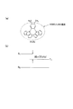
- 1 and 2 are schematic diagrams showing energy diagrams of a compound that expresses a TADF phenomenon (TADF compound) and a general fluorescent compound.
- TADF compound TADF compound
- 2CzPN having the structure shown in FIG. 1 HOMO is localized at the 1st and 2nd carbazolyl groups on the benzene ring, and LUMO is localized at the 4th and 5th cyano groups. Therefore, it is possible to separate the HOMO and LUMO of 2CzPN, ⁇ E ST express TADF phenomenon extremely small.
- 2CzXy FIG.
- the present invention has been made in view of the above problems and situations, and a problem to be solved is, for example, to provide a new ⁇ -conjugated compound that can improve the light emission efficiency of an organic electroluminescence element.
- an organic electroluminescence element material, a light emitting material, a charge transport material, a light-emitting thin film, an organic electroluminescence element, and a display device and an illumination device provided with the organic electroluminescence element using the ⁇ -conjugated compound are provided. It is to be.
- L and M each independently represent an electron donating group D or an electron withdrawing group A;
- the electron donating group D is a group selected from the group consisting of an aryl group substituted with an electron donating group, a heterocyclic group of an electron donating group which may be substituted, and an amino group which may be substituted.
- the electron withdrawing group A includes an optionally substituted carbonyl group, an optionally substituted sulfonyl group, an optionally substituted phosphine oxide group, an optionally substituted boryl group, and an electron withdrawing group.
- Each Q independently represents a carbon atom or a nitrogen atom;
- R represents a carbon atom, an oxygen atom, a nitrogen atom, a sulfur atom, a boron atom or a silicon atom.
- the electron donating group D is an aryl group substituted with an electron donating group or a heterocyclic group of an electron donating group which may be substituted, ⁇ according to [1] or [2] Conjugated compounds.
- the electron withdrawing group A is an aryl group optionally substituted with an electron withdrawing group, an electron donating heterocyclic group substituted with an electron withdrawing group, or substituted.
- an absolute value of the lowest Delta] E ST of the energy difference between the excited singlet state and the lowest excited triplet level is below 0.50eV, [1] ⁇ ⁇ conjugated compound according to any one of [4] .
- [12] including an anode, a cathode, and a light emitting layer provided between the anode and the cathode, An organic electroluminescence device, wherein at least one layer of the light emitting layer includes the ⁇ -conjugated compound according to any one of [1] to [5].
- [13] The organic electroluminescence device according to [12], wherein the ⁇ -conjugated compound generates excitons.
- [15] The organic electroluminescence device according to [14], wherein the ⁇ -conjugated compound emits delayed fluorescence.
- X 101 represents NR 101 , an oxygen atom, a sulfur atom, a sulfinyl group, a sulfonyl group, CR 102 R 103 or SiR 104 R 105 , y 1 to y 8 each independently represent CR 106 or a nitrogen atom; R 101 to R 106 each independently represents a hydrogen atom or a substituent, and may be bonded to each other to form a ring; Ar 101 and Ar 102 each independently represents an optionally substituted aryl group or an optionally substituted heteroaryl group; n101 and n102 each represents an integer of 0 to 4.
- n 101 represents an integer of 1 to 4.
- X 101 represents NR 101 , an oxygen atom, a sulfur atom, a sulfinyl group, a sulfonyl group, CR 102 R 103 or SiR 104 R 105 , R 101 to R 105 each represent a hydrogen atom or a substituent, and may be bonded to each other to form a ring; Ar 101 and Ar 102 each independently represents an optionally substituted aryl group or an optionally substituted heteroaryl group; n102 represents an integer of 0 to 4. )
- a display device comprising the organic electroluminescence element according to any one of [12] to [20].
- a lighting device comprising the organic electroluminescence element according to any one of [12] to [20].
- the above-mentioned means of the present invention can provide a new ⁇ -conjugated compound that can improve the light emission efficiency of, for example, an organic electroluminescence device. Furthermore, the above-mentioned means of the present invention can provide a new organic electroluminescence device that realizes an improvement in luminous efficiency.
- an organic electroluminescent element material, a light-emitting thin film, a luminescent material, and a display device and a lighting device including the organic electroluminescent element using the ⁇ -conjugated compound can be provided.
- ⁇ is used to mean that the numerical values described before and after it are included as a lower limit value and an upper limit value.
- the present inventor has the electron-donating groups D, the electron-withdrawing groups A, or the electron-donating group D and the electrons.
- a molecular design having 2 or 3 ring structures in which 3 to 5 atoms exist between the attractive groups A and all of these 3 to 5 atoms are included as ring constituent atoms
- the TADF phenomenon can be further expressed.
- the ring structure Is an electron withdrawing ring.
- the ring structure is an electron donating ring.
- Two or three ring structures mean a condensed ring in which two or three monocyclic aromatic rings are condensed. It is known that it is necessary to separate HOMO and LUMO to form a CT excited state in order to further develop the TADF phenomenon.
- the electron donating part and the electron withdrawing part are in charge-separated state in the CT excited state that expresses TADF.
- the ⁇ -conjugated compound of the present invention has an electron donating group D and an electron withdrawing group A, a ring structure containing 3 to 5 atoms between the electron donating group D and the electron withdrawing group A
- the electron-donating group D and the electron-withdrawing group A can spatially face each other at an angle close to parallel in the excited state.
- a CT excited state can be effectively formed and stabilized.
- it is considered that non-radiation deactivation can be suppressed and luminous efficiency can be increased.
- such a ⁇ -conjugated compound so may the Delta] E ST minimized, it is considered possible to further increase the luminous efficiency.
- the electron-donating group D and the electron-withdrawing group A face each other at an angle close to parallel in space as in the present invention
- the electron-donating group D and the electron-withdrawing group A located in the very vicinity are It is considered that a CT-type excited state is formed in the interval (that is, through space).
- the CT excited state is stabilized and the non-radiation deactivation can be suppressed as compared with the prior art, which is considered advantageous in the expression of high luminous efficiency by the organic electroluminescence element.
- one of L and M is the electron donating group D
- the other is the electron withdrawing group A.
- the compound has both an electron donating group D and an electron-withdrawing group a, it can be reduced Delta] E ST, preferable in achieving high luminous efficiency.
- a strong electron donating group or electron withdrawing group can be used. It is preferable because high luminous efficiency can be achieved. Thereby, it is considered that the wavelength increase of the absorption spectrum and the emission spectrum can be suppressed.
- ⁇ -conjugated compound of the present invention is a compound having a structure represented by any one of the following general formulas (1) to (6).
- L and M each independently represent an electron donating group D or an electron withdrawing group A.
- the electron donating group D represented by L or M is an “aryl group substituted with an electron donating group” or “an optionally substituted electron donating group”. It can be a “heterocyclic group” or an “optionally substituted amino group”.
- the “aryl group” in the “aryl group substituted with an electron donating group” represented by D is preferably a group derived from an aromatic hydrocarbon ring having 6 to 24 carbon atoms.
- aromatic hydrocarbon rings include benzene ring, indene ring, naphthalene ring, azulene ring, fluorene ring, phenanthrene ring, anthracene ring, acenaphthylene ring, biphenylene ring, naphthacene ring, pyrene ring, pentalene ring, ASEAN Tolylene ring, heptalene ring, triphenylene ring, as-indacene ring, chrysene ring, s-indacene ring, preaden ring, phenalene ring, fluoranthene ring, perylene ring, acephenanthrylene ring, biphenyl ring, terphenyl ring,
- a benzene ring, naphthalene ring, fluorene ring, phenanthrene ring, anthracene ring, biphenylene ring, chrysene ring, pyrene ring, triphenylene ring, chrysene ring, fluoranthene ring, perylene ring, biphenyl ring and terphenyl ring are mentioned.
- the “electron-donating group” in the “aryl group substituted with an electron-donating group” represented by D is an alkyl group, an alkoxy group, an optionally substituted amino group, or an optionally substituted electron donor. Sex heterocyclic groups and the like. Preferable examples include an optionally substituted alkyl group and an optionally substituted heterocyclic group of an electron donating group.
- alkyl group of the “electron-donating group” in the “aryl group substituted with an electron-donating group” represented by D may be linear, branched, or cyclic. 20 linear, branched, or cyclic alkyl groups, such as methyl group, ethyl group, n-propyl group, isopropyl group, n-butyl group, s-butyl group, t-butyl group, n-pentyl, neopentyl, n-hexyl, cyclohexyl, 2-ethylhexyl, n-heptyl, n-octyl, 2-hexyloctyl, n-nonyl, n-decyl, n-undecyl Group, n-dodecyl group, n-tridecyl group, n-tetradecyl group, n-pentadecyl group,
- the “alkoxy group” of the “electron-donating group” of the “aryl group substituted with an electron-donating group” represented by D may be linear, branched, or cyclic. 20 linear, branched, or cyclic alkyl groups are mentioned, specifically, methoxy group, ethoxy group, n-propoxy group, isopropoxy group, n-butoxy group, isobutoxy group, t-butoxy group, n -Pentyloxy group, neopentyloxy group, n-hexyloxy group, cyclohexyloxy group, n-heptyloxy group, n-octyloxy group, 2-ethylhexyloxy group, nonyloxy group, decyloxy group, 3,7-dimethyloctyl Oxy group, n-undecyloxy group, n-dodecyloxy group, n-tridecyloxy group, n-tetrade
- the substituent of the “optionally substituted amino group” of the “electron-donating group” of the “aryl group substituted with an electron-donating group” represented by D is an alkyl group or an alkyl group.
- an alkyl group and an aryl group have the same meanings as the aforementioned alkyl group and aryl group, respectively.
- the “electron-donating heterocyclic group” in the “optionally substituted electron-donating heterocyclic group” represented by D is derived from an electron-donating heterocyclic ring having 4 to 24 carbon atoms. It is preferably a group.
- heterocycles include pyrrole, indole, carbazole, azacarbazole, diazacarbazole, indoloindole, 9,10-dihydroacridine, 10,11-dihydrodibenzazepine, 5 , 10-dihydrodibenzoazacillin, phenoxazine ring, phenothiazine ring, dibenzothiophene ring, benzofurylindole ring, benzothienoindole ring, indolocarbazole ring, benzofurylcarbazole ring, benzothienocarbazole ring, benzothienobenzothiophene ring, A benzocarbazole
- the electron-donating heterocyclic group may be a group in which two or more of the same or different heterocyclic rings are bonded via a single bond.
- Examples of the substituent in the “optionally substituted electron-donating heterocyclic group” represented by D include an alkyl group, an alkoxy group, an aryl ring which may be substituted with an alkyl group, and an optionally substituted group.
- An amino group etc. are mentioned.
- the alkyl group, alkoxy group, aryl group and amino group have the same meanings as the alkyl group, alkoxy group, aryl group and amino group, respectively.
- the “optionally substituted electron-donating heterocyclic group” of the “electron-donating group” of the “aryl group substituted with an electron-donating group” represented by D is the above-mentioned “substituted” group. It is synonymous with “a good electron-donating heterocyclic group”.
- Examples of the substituent in the “optionally substituted amino group” represented by D include an alkyl group and an aryl group optionally substituted with an alkyl group.
- the alkyl group and the aryl group may be the same as the aforementioned alkyl group and aryl group, respectively.
- the electron donating group D is a phenyl group substituted with an electron donating group, an optionally substituted carbazolyl group, an optionally substituted azacarbazolyl group, and a substituted group.
- an optionally substituted carbazolyl group an optionally substituted azacarbazolyl group, an optionally substituted diazacarbazolyl group, an optionally substituted 9,10-dihydroacridyl group, It is an optionally substituted diphenylamino group.
- the electron withdrawing group A represented by L or M is “an optionally substituted carbonyl group”, “an optionally substituted sulfonyl group”, “a substituted” Phosphine oxide group which may be substituted ",” boryl group which may be substituted “,” aryl group which may be substituted with electron withdrawing group ",” electron substituted with electron withdrawing group " It may be “a donating heterocyclic group” or “an electron-withdrawing heterocyclic group which may be substituted”.
- aryl group of the “aryl group optionally substituted with an electron withdrawing group” represented by A has the same meaning as the above-described aryl group.
- Examples of the substituent of the “aryl group optionally substituted with an electron withdrawing group” represented by A include a fluorine atom, a cyano group, an alkyl group optionally substituted with a fluorine atom, and optionally substituted.
- a fluorine atom, a cyano group, an alkyl group substituted with a fluorine atom, or an optionally substituted electron-withdrawing heterocyclic group is preferable.
- the “electron-donating heterocyclic group” in the “electron-donating heterocyclic group substituted with an electron-withdrawing group” represented by A is the above-mentioned “optionally substituted D”. It is synonymous with “electron-donating heterocyclic group” in “electron-donating heterocyclic group”.
- the “electron-withdrawing group” that is a substituent of the “electron-donating heterocyclic group substituted with an electron-withdrawing group” represented by A has the same meaning as the substituent for the aryl group described above. .
- heterocyclic group in the “optionally substituted electron-withdrawing heterocyclic group” represented by A is a group derived from an electron-withdrawing heterocyclic group having 3 to 24 carbon atoms. preferable.
- heterocycles include dibenzothiophene oxide ring, dibenzothiophene dioxide ring, pyridine ring, pyridazine ring, pyrimidine ring, pyrazine ring, triazine ring, quinoline ring, isoquinoline ring, quinazoline ring, cinnoline ring, quinoxaline ring Phthalazine ring, pteridine ring, phenanthridine ring, phenanthroline ring, dibenzofuran ring, dibenzosilole ring, dibenzoborol ring, azadibenzofuran ring, diazadibenzofuran ring, dibenzophosphole oxide ring and the like.
- the electron-withdrawing heterocyclic group may be a group in which two or more of the same or different heterocyclic rings are bonded via a single bond.
- Examples of the substituent in the “optionally withdrawing heterocyclic group with electron withdrawn” represented by A include a deuterium atom, a fluorine atom, a cyano group, an alkyl group optionally substituted with a fluorine atom, fluorine Examples thereof include an aryl group which may be substituted with an alkyl group which may be substituted with an atom, and an aryl group which may be substituted with a fluorine atom.
- An alkyl group and an aryl group are synonymous with the above-mentioned alkyl group and aryl group.
- the “optionally substituted electron-withdrawing heterocyclic group” of the “aryl group optionally substituted with an electron-withdrawing group” represented by A has the same meaning as described above.
- substituents include a fluorine atom, a cyano group, an alkyl group that may be substituted with a fluorine atom, an aryl group that may be substituted, and an electron-withdrawing heterocyclic ring that may be substituted.
- An alkyl group and an aryl group are synonymous with the above-mentioned alkyl group and aryl group.
- L and M each independently represent an electron donating group D or an electron withdrawing group A. Therefore, the ⁇ -conjugated compound having a structure represented by any one of the general formulas (1) to (6) may have two electron donating groups D (or electron donating groups A), You may have both the electron-donating group D and the electron-donating group A.
- the ring to which L and M are bonded is an electron-withdrawing ring; both L and M are electron-withdrawing groups A In some cases, the ring to which L and M are bonded is an electron-donating ring.
- examples in which the ring to which L and M are bonded are “electron-donating rings” include the carbazole ring in the general formula (1), the carbazole ring in the general formula (3), The indoloindole ring in the general formula (5) and the indolocarbazole ring in the general formula (6) are included.
- one of L and M is an electron donating group D
- the other is an electron withdrawing group A
- the compound is an electron donating group D and an electron withdrawing group A.
- it has both attracting group a is preferable for possible smaller Delta] E ST, to achieve high luminous efficiency.
- a strong electron donating group or electron withdrawing group can be used. It is preferable because high luminous efficiency can be achieved. Thereby, it is considered that the wavelength increase of the absorption spectrum and the emission spectrum can be suppressed.
- each Q independently represents a carbon atom or a nitrogen atom.
- 6 to 10 Qs are included, and among them, the number of nitrogen atoms is preferably 0 to 4, more preferably 0 to 2. It is preferable from the viewpoint of controlling the emission wavelength that the number of nitrogen atoms contained as Q is 2 or less.
- the substituent of the carbon atom is a hydrogen atom, a deuterium atom, a fluorine atom, a cyano group, or an alkyl group optionally substituted with fluorine.
- R represents a carbon atom, an oxygen atom, a nitrogen atom, a sulfur atom, a boron atom, or a silicon atom, preferably a carbon atom, an oxygen atom, a nitrogen atom, or a silicon atom, and more preferably Are an oxygen atom and a nitrogen atom. From the viewpoints of luminescence and synthesis, R is preferably an oxygen atom or a nitrogen atom.
- R when R is a carbon atom, a nitrogen atom, a boron atom or a silicon atom, R may be substituted. Since the ⁇ -conjugated compound having the structure represented by the general formula (3) has an electron donating group D and / or an electron withdrawing group A as L and M, the substituent of R is L And the electron donating groups D as M, the electron withdrawing groups A, or the interaction between the electron donating group D and the electron withdrawing group A are preferably not disturbed.
- substituents include alkyl groups (for example, methyl group, ethyl group, propyl group, isopropyl group, tert-butyl group, pentyl group, hexyl group, octyl group, dodecyl group, tridecyl group, tetradecyl group, pentadecyl group).
- alkyl groups for example, methyl group, ethyl group, propyl group, isopropyl group, tert-butyl group, pentyl group, hexyl group, octyl group, dodecyl group, tridecyl group, tetradecyl group, pentadecyl group.
- cycloalkyl groups for example, cyclopentyl group, cyclohexyl group, etc.
- aryl groups for example, phenyl group, p-chlorophenyl group, mesityl group, tolyl group, xylyl group, naphthyl group, anthryl group, azulenyl group, acenaphthenyl group
- aromatic heterocyclic group for example, pyridyl group, pyrimidinyl group, furyl group, pyrrolyl group, imidazolyl group, benzimidazolyl group, pyrazolyl group, pyrazinyl group, Triazolyl groups (eg 1,2,4-triazol-1-yl group, 1,2,3-triazol-1-yl group, pyrrolidy
- R is preferably an aryl group or an alkyl group because electronic perturbation of L and M is small.
- the ⁇ -conjugated compound having the structure of formula (1) has an electron donating group D and an electron withdrawing group A, two electron donating groups D, or two electron withdrawing groups A in space. It is easy to meet at an angle close to parallel at a position close to. Thus, CT of the excited state tends to be formed between the electron-donating group D and an electron-withdrawing group A, Delta] E ST Decrease or; two electron-donating group D or between two electron withdrawing This is because the sex groups A easily resonate with each other and can easily stabilize the excited state.
- the ⁇ -conjugated compound having the structure represented by any one of the general formulas (1) to (6) includes an organic electroluminescence element material containing the ⁇ -conjugated compound and light emission containing the ⁇ -conjugated compound. It can be used as an organic electroluminescence device containing a conductive thin film and the ⁇ -conjugated compound.
- the ⁇ -conjugated compound having the structure represented by any one of the general formulas (1) to (6) can be excited by electric field excitation to generate excitons. Accordingly, the ⁇ -conjugated compound having a structure represented by any one of the general formulas (1) to (6) is preferably included in the light emitting layer of the organic electroluminescence device.
- a ⁇ -conjugated compound having a structure represented by any one of the general formulas (1) to (6) is used alone; A ⁇ -conjugated compound having a structure represented by any one of (6) and a host compound described later; a ⁇ -conjugated having a structure represented by any one of the general formulas (1) to (6) A ⁇ -conjugate having a structure represented by any one of the general formulas (1) to (6), or a compound containing at least one of a fluorescent compound and a phosphorescent compound to be described later; It is preferable to contain a system compound, at least one of a fluorescent compound and a phosphorescent compound described below, and a host compound described below.
- the absolute value ( ⁇ E ST ) of the energy difference between the lowest excited singlet level and the lowest excited triplet level of the ⁇ -conjugated compound having the structure represented by any one of the general formulas (1) to (6) is , 0.50 eV or less is preferable.
- the ⁇ -conjugated compound of the present invention is preferably contained in the organic electroluminescent element, the element material, or the light-emitting thin film.
- the organic electroluminescence element of the present invention can be suitably provided in a lighting device and a display device.
- ⁇ -conjugated compounds according to the present invention are shown below. However, these compounds may further have a substituent or may have a structural isomer, and are limited to this description. Not.
- TADF resistance delay fluorescent
- exhibiting delayed fluorescence means that there are two or more types of components having different decay rates of emitted fluorescence when fluorescence decay measurement is performed.
- the slow decay component generally has a decay time of sub-microseconds or more.
- the decay time is not limited because the decay time differs depending on the material.
- fluorescence decay measurement can be performed as follows.
- a solution or thin film of a ⁇ -conjugated compound (luminescent compound) or a co-deposition film of the ⁇ -conjugated compound and the second component is irradiated with excitation light in a nitrogen atmosphere, and the number of photons at a certain emission wavelength is measured.
- the ⁇ -conjugated compound exhibits delayed fluorescence when there are two or more types of components having different decay rates of emitted fluorescence.
- these compounds have bipolar properties and can cope with various energy levels, they can be used not only as light emitting materials and host materials, but also suitable for hole transport and electron transport, Since it can be used as a charge transport material, it is not limited to use in a light emitting layer, and the above-described hole injection layer, hole transport layer, electron blocking layer, hole blocking layer, electron transport layer, electron injection layer And may be used for an intermediate layer or the like.
- Organic EL emission methods There are two types of organic EL emission methods: “phosphorescence emission” that emits light when returning from the triplet excited state to the ground state, and “fluorescence emission” that emits light when returning from the singlet excited state to the ground state. is there.
- phosphorescence emission that emits light when returning from the triplet excited state to the ground state
- fluorescence emission that emits light when returning from the singlet excited state to the ground state.
- TTA triplet-triplet annealing
- the rate constant is usually small. That is, since the transition is difficult to occur, the exciton lifetime is increased from millisecond to second order, and it is difficult to obtain desired light emission.
- the rate constant of the forbidden transition increases by 3 digits or more due to the heavy atom effect of the central metal. % Phosphorescence quantum yield can be obtained.
- a rare metal called a white metal such as iridium, palladium, or platinum, which is a rare metal. The price of the metal itself is a major industrial issue.
- a general fluorescent compound is not necessarily a heavy metal complex like a phosphorescent compound, and is a so-called organic compound composed of a combination of general elements such as carbon, oxygen, nitrogen and hydrogen.
- other non-metallic elements such as phosphorus, sulfur, and silicon can be used, and complexes of typical metals such as aluminum and zinc can be used.
- high efficiency light emission such as phosphorescence emission cannot be expected.
- TTA triplet-triplet annihilation
- Thermal activated delayed fluorescence (TADF) compound which is another highly efficient fluorescent emission, is a method that can solve the problems of TTA.
- the fluorescent compound has the advantage that the molecule can be designed infinitely. That is, among the molecularly designed compounds, there are compounds in which the energy level difference between the triplet excited state and the singlet excited state is extremely close. Such compounds, even though in the molecule does not have a heavy atom, reverse intersystem crossing from a triplet excited state is usually not occur because Delta] E ST is smaller to the singlet excited state occurs.
- Rigidity described here means that there are few sites that can move freely in the molecule, for example, by suppressing free rotation in the bond between the rings in the molecule or by introducing a condensed ring with a large ⁇ conjugate plane. means. In particular, it is possible to reduce the structural change in the excited state by making the portion involved in light emission rigid.
- the ⁇ -conjugated compound of the present invention contains 3 to 5 atoms between the electron donating groups D, between the electron withdrawing groups A, or between the electron donating group D and the electron withdrawing group A.
- HOMO and LUMO have been successfully separated.
- the electron donating groups D, the electron withdrawing groups A, or the electron donating groups D and the electron withdrawing groups A face each other at an angle close to parallel. Therefore, it is considered that a CT excited state can be effectively formed and stabilized. As a result, it is considered that the non-radiative deactivation of the compound of the present application can be suppressed and the luminous efficiency can be improved.
- the electron-withdrawing group A and the electron-donating group D interact with each other in the through space, not through the through bond. It is considered that the wavelength can be suppressed.
- [Electron density distribution] ⁇ conjugated compound according to the present invention from the viewpoint of reducing the Delta] E ST, it is preferable that HOMO and LUMO are substantially separated in the molecule.
- the distribution states of these HOMO and LUMO can be obtained from the electron density distribution when the structure is optimized by molecular orbital calculation.
- structure optimization and calculation of electron density distribution by molecular orbital calculation of ⁇ -conjugated compounds in the present invention are performed using molecular orbital calculation software using B3LYP as a functional and 6-31G (d) as a basis function as a calculation method.
- B3LYP molecular orbital calculation software
- 6-31G (d) as a basis function as a calculation method.
- Gaussian 09 Revision C.01, MJ Frisch, et al, Gaussian, Inc., 2010. manufactured by Gaussian, USA was used as molecular orbital calculation software.
- HOMO and LUMO are substantially separated means that the HOMO orbital distribution calculated by the above molecular calculation and the central part of the LUMO orbital distribution are separated, more preferably the HOMO orbital distribution and the LUMO orbital. This means that the distributions of do not overlap.
- the separation state of HOMO and LUMO from the above-mentioned structure optimization calculation using B3LYP as the functional and 6-31G (d) as the basis function, the time-dependent density functional method (Time-Dependent DFT) is used.
- the lowest excited singlet energy level S 1 of the ⁇ -conjugated compound in the present invention is defined in the present invention as calculated in the same manner as in a normal method. That is, a sample to be measured is deposited on a quartz substrate to prepare a sample, and the absorption spectrum (vertical axis: absorbance, horizontal axis: wavelength) of this sample is measured at room temperature (300 K). A tangent line is drawn with respect to the rising edge of the absorption spectrum on the long wavelength side, and is calculated from a predetermined conversion formula based on the wavelength value at the intersection of the tangent line and the horizontal axis.
- the molecules themselves of the ⁇ -conjugated compound used in the present invention have a relatively high aggregation property, an error due to aggregation may occur in the measurement of the thin film.
- the lowest excited singlet energy level S 1 in the present invention is room temperature (25 ° C.
- the peak value of the maximum emission wavelength in the solution state of the ⁇ -conjugated compound in (1) was used as an approximate value.
- a solvent that does not affect the aggregation state of the ⁇ -conjugated compound that is, a solvent having a small influence of the solvent effect, for example, a nonpolar solvent such as cyclohexane or toluene can be used.
- the lowest excited triplet energy level (T 1 ) of the ⁇ -conjugated compound used in the present invention was calculated from the photoluminescence (PL) characteristics of the solution or thin film.
- PL photoluminescence
- the transient PL characteristics are measured to separate the fluorescent component and the phosphorescent component, the absolute value of the energy difference can be determined the lowest excited triplet energy level of the lowest excited singlet energy level as Delta] E ST.
- an absolute PL quantum yield measuring apparatus C9920-02 manufactured by Hamamatsu Photonics
- the light emission lifetime was measured using a streak camera C4334 (manufactured by Hamamatsu Photonics) while exciting the sample with laser light.
- the organic EL device of the present invention is an organic electroluminescence device having at least a light emitting layer between an anode and a cathode, and at least one of the light emitting layers is any one of the general formulas (1) to (7). It contains a ⁇ -conjugated compound having the structure represented.
- the following structures can be exemplified, but the invention is not limited thereto.
- Anode / light emitting layer / cathode (2) Anode / light emitting layer / electron transport layer / cathode (3) Anode / hole transport layer / light emitting layer / cathode (4) Anode / hole transport layer / light emitting layer / electron Transport layer / cathode (5) Anode / hole transport layer / light emitting layer / electron transport layer / electron injection layer / cathode (6) Anode / hole injection layer / hole transport layer / light emitting layer / electron transport layer / cathode ( 7) Anode / hole injection layer / hole transport layer / (electron blocking layer /) luminescent layer / (hole blocking layer /) electron transport layer / electron injection layer / cathode Among the above, the configuration of (7) is preferable.
- the light emitting layer used in the present invention is composed of a single layer or a plurality of layers. When there are a plurality of light emitting layers, a non-light emitting intermediate layer may be provided between the light emitting layers.
- a hole blocking layer also referred to as a hole barrier layer
- an electron injection layer also referred to as a cathode buffer layer
- An electron blocking layer also referred to as an electron barrier layer
- a hole injection layer also referred to as an anode buffer layer
- the electron transport layer used in the present invention is a layer having a function of transporting electrons, and in a broad sense, an electron injection layer and a hole blocking layer are also included in the electron transport layer. Moreover, you may be comprised by multiple layers.
- the hole transport layer used in the present invention is a layer having a function of transporting holes, and in a broad sense, a hole injection layer and an electron blocking layer are also included in the hole transport layer. Moreover, you may be comprised by multiple layers. In the above-described typical element configuration, the layer excluding the anode and the cathode is also referred to as “organic layer”.
- the organic EL element of the present invention may be a so-called tandem element in which a plurality of light emitting units including at least one light emitting layer are stacked.
- a tandem element in which a plurality of light emitting units including at least one light emitting layer are stacked.
- the first light emitting unit, the second light emitting unit and the third light emitting unit are all the same, May be different.
- Two light emitting units may be the same, and the remaining one may be different.
- a plurality of light emitting units may be laminated directly or via an intermediate layer, and the intermediate layer is generally an intermediate electrode, an intermediate conductive layer, a charge generation layer, an electron extraction layer, a connection layer, an intermediate layer.
- a known material structure can be used as long as it is also called an insulating layer and has a function of supplying electrons to the anode-side adjacent layer and holes to the cathode-side adjacent layer.
- Examples of materials used for the intermediate layer include ITO (indium tin oxide), IZO (indium zinc oxide), ZnO 2 , TiN, ZrN, HfN, TiOx, VOx, CuI, InN, GaN, CuAlO 2 , Conductive inorganic compound layers such as CuGaO 2 , SrCu 2 O 2 , LaB 6 , RuO 2 and Al, two-layer films such as Au / Bi 2 O 3 , SnO 2 / Ag / SnO 2 , ZnO / Ag / ZnO , Bi 2 O 3 / Au / Bi 2 O 3 , TiO 2 / TiN / TiO 2 , TiO 2 / ZrN / TiO 2 and other multilayer films, C 60 and other fullerenes, conductive organic layers such as oligothiophene, Examples include conductive organic compound layers such as metal phthalocyanines, metal-free phthalocyanines, metal porphyrins, metal-free
- tandem organic EL element examples include, for example, US Pat. No. 6,337,492, US Pat. No. 7,420,203, US Pat. No. 7,473,923, US Pat. No. 6,872,472, US Pat. No. 6,107,734. Specification, U.S. Pat. No. 6,337,492, International Publication No.
- the light-emitting layer used in the present invention is a layer that provides a field in which electrons and holes injected from an electrode or an adjacent layer are recombined to emit light via excitons, and the light-emitting portion is the light-emitting layer Even in the layer, it may be the interface between the light emitting layer and the adjacent layer. If the light emitting layer used for this invention satisfy
- the total thickness of the light emitting layer is not particularly limited, but it prevents the uniformity of the film to be formed, the application of unnecessary high voltage during light emission, and the improvement of the stability of the emission color against the drive current.
- each light emitting layer used in the present invention is preferably adjusted to a range of 2 nm to 5 ⁇ m, more preferably adjusted to a range of 2 to 500 nm, and further preferably adjusted to a range of 5 to 200 nm.
- the thickness of each light emitting layer used in the present invention is preferably adjusted to a range of 2 nm to 1 ⁇ m, more preferably adjusted to a range of 2 to 200 nm, and further preferably in a range of 3 to 150 nm. Adjusted.
- the light emitting layer used in the present invention may be composed of a single layer or a plurality of layers.
- the ⁇ -conjugated compound of the present application When used for the light emitting layer, it may be used alone or in combination with a host material, a fluorescent light emitting material, a phosphorescent light emitting material, etc. described later. At least one layer of the light emitting layer contains a light emitting dopant (a light emitting compound, a light emitting dopant, also simply referred to as a dopant), and further contains a host compound (a matrix material, a light emitting host compound, also simply referred to as a host). Is preferred.
- a light emitting dopant a light emitting compound, a light emitting dopant, also simply referred to as a dopant
- a host compound a matrix material, a light emitting host compound, also simply referred to as a host. Is preferred.
- At least one layer of the light-emitting layer contains the ⁇ -conjugated compound of the present application and a host compound because luminous efficiency is improved. It is preferable that at least one layer of the light-emitting layer contains the ⁇ -conjugated compound of the present application and at least one of a fluorescent compound and a phosphorescent compound because luminous efficiency is improved. It is preferable that at least one layer of the light emitting layer contains the present ⁇ -conjugated compound, at least one of a fluorescent light emitting compound and a phosphorescent light emitting compound, and a host compound because the light emission efficiency is improved.
- the luminescent dopant As the luminescent dopant, a fluorescent luminescent dopant (also referred to as a fluorescent luminescent compound or a fluorescent dopant) and a phosphorescent dopant (also referred to as a phosphorescent luminescent compound or a phosphorescent dopant) are preferably used. It is done.
- the light-emitting layer contains the ⁇ -conjugated compound according to the present invention as a fluorescent light-emitting compound or an assist dopant in a range of 0.1 to 50% by mass, particularly in a range of 1 to 30% by mass. It is preferable to contain within.
- the light emitting layer contains the light emitting compound within a range of 0.1 to 50% by mass, and particularly preferably within a range of 1 to 30% by mass.
- concentration of the light-emitting compound in the light-emitting layer can be arbitrarily determined based on the specific light-emitting compound used and the requirements of the device, and is uniform in the thickness direction of the light-emitting layer. It may be contained and may have any concentration distribution.
- the luminescent compound used in the present invention may be used in combination of two or more types, a combination of fluorescent luminescent compounds having different structures, or a combination of a fluorescent luminescent compound and a phosphorescent luminescent compound. May be. Thereby, arbitrary luminescent colors can be obtained.
- the absolute value ( ⁇ E ST ) of the difference between the lowest excited singlet energy level and the lowest excited triplet energy level is 0.50 eV or less, a ⁇ -conjugated compound according to the present invention, a luminescent compound, and a host compound.
- the ⁇ -conjugated compound according to the present invention acts as an assist dopant.
- the ⁇ -conjugated compound according to the present invention acts as a host compound.
- the ⁇ -conjugated compound according to the present invention acts as a host compound / light-emitting compound.
- the mechanism for producing the effect is the same in any case, and the triplet exciton generated on the ⁇ -conjugated compound according to the present invention is converted into a singlet exciton by reverse intersystem crossing (RISC). It is in.
- RISC reverse intersystem crossing
- all the exciton energies generated on the ⁇ -conjugated compound according to the present invention can be transferred to the luminescent compound by fluorescence resonance energy transfer (FRET), thereby realizing high luminous efficiency.
- FRET fluorescence resonance energy transfer
- the energy levels of S 1 and T 1 of the ⁇ -conjugated compound are S of the host compound. 1 and T 1 of the lower than the energy level, it is preferably higher than the energy level of the S 1 and T 1 of the light-emitting compound.
- FIG. 3 and FIG. 4 show schematic diagrams when the ⁇ -conjugated compound of the present invention acts as an assist dopant and a host compound, respectively.
- 3 and 4 are examples, and the generation process of the triplet exciton generated on the ⁇ -conjugated compound according to the present invention is not limited to the electric field excitation, and the energy transfer from the light emitting layer or the peripheral layer interface. And electronic transfer.
- a fluorescent compound is used as a light-emitting material, but the present invention is not limited to this, and a phosphorescent compound may be used, or a fluorescent compound and a phosphorescent compound may be used. Both of the functional compounds may be used.
- the light-emitting layer contains a host compound in a mass ratio of 100% or more with respect to the ⁇ -conjugated compound, and the fluorescent compound and / or phosphorescent compound. Is preferably contained within a range of 0.1 to 50% by mass with respect to the ⁇ -conjugated compound.
- the light emitting layer has a mass ratio of 0.1 to 50% of the fluorescent compound and / or phosphorescent compound with respect to the ⁇ -conjugated compound. It is preferable to contain.
- the emission spectrum of the ⁇ -conjugated compound according to the present invention and the absorption spectrum of the luminescent compound preferably overlap.
- the light emission color of the organic EL device of the present invention and the compound used in the present invention is shown in FIG. 3.16 on page 108 of “New Color Science Handbook” (edited by the Japan Color Society, University of Tokyo Press, 1985). It is determined by the color when the result measured with a luminance meter CS-1000 (manufactured by Konica Minolta Co., Ltd.) is applied to the CIE chromaticity coordinates.
- the light emitting layer of one layer or a plurality of layers contains a plurality of light emitting dopants having different emission colors and emits white light.
- Fluorescent luminescent dopant (1.1) Fluorescent luminescent dopant
- the ⁇ -conjugated compound of the present invention may be used as the fluorescent luminescent dopant (fluorescent dopant), or a known fluorescent dopant or delayed fluorescence used in the light emitting layer of the organic EL device. You may use it, selecting suitably from sex dopant.
- the phosphorescent dopant used in the present invention is a compound in which light emission from an excited triplet is observed, specifically, a compound that emits phosphorescence at room temperature (25 ° C.), and a phosphorescence quantum yield. Is defined as a compound of 0.01 or more at 25 ° C., but a preferable phosphorescence quantum yield is 0.1 or more.
- the phosphorescence quantum yield can be measured by the method described in Spectroscopic II, page 398 (1992 edition, Maruzen) of Experimental Chemistry Course 4 of the 4th edition. Although the phosphorescence quantum yield in a solution can be measured using various solvents, the phosphorescence dopant used in the present invention achieves the phosphorescence quantum yield (0.01 or more) in any solvent. Just do it.
- the phosphorescent dopant can be appropriately selected from known materials used for the light emitting layer of the organic EL device.
- Specific examples of known phosphorescent dopants that can be used in the present invention include compounds described in the following documents. Nature 395, 151 (1998), Appl. Phys. Lett. 78, 1622 (2001), Adv. Mater. 19, 739 (2007), Chem. Mater. 17, 3532 (2005), Adv. Mater. 17, 1059 (2005), International Publication No. 2009/100991, International Publication No. 2008/101842, International Publication No. 2003/040257, US Patent Application Publication No. 2006/835469, US Patent Application Publication No. 2006 /. No. 0202194, U.S. Patent Application Publication No.
- a preferable phosphorescent dopant includes an organometallic complex having Ir as a central metal. More preferably, a complex containing at least one coordination mode of metal-carbon bond, metal-nitrogen bond, metal-oxygen bond, and metal-sulfur bond is preferable.
- the host compound used in the present invention is a compound mainly responsible for charge injection and transport in the light emitting layer, and its own light emission is not substantially observed in the organic EL device.
- the host compound preferably has a mass ratio in the layer of 20% or more among the compounds contained in the light emitting layer.
- a host compound may be used independently or may be used in combination of multiple types. By using a plurality of types of host compounds, it is possible to adjust the movement of charges, and the efficiency of the organic electroluminescence element can be improved.
- the host compound that is preferably used in the present invention will be described below.
- the ⁇ -conjugated compound used in the present invention may be used as described above, but there is no particular limitation. From the viewpoint of reverse energy transfer, those having an excitation energy larger than the excitation singlet energy of the dopant are preferred, and those having an excitation triplet energy larger than the excitation triplet energy of the dopant are more preferred.
- the host compound is responsible for carrier transport and exciton generation in the light emitting layer. Therefore, it can exist stably in all active species states such as cation radical state, anion radical state, and excited state, and does not cause chemical changes such as decomposition and addition reaction. It is preferable not to move at the angstrom level.
- the existence time of the triplet excited state of the TADF compound is long, so that the T 1 energy level of the host compound itself is high, and the host compounds are associated with each other.
- Molecules in which the host compound does not decrease in T 1 such as not forming a low T 1 state in the state, TADF compound and the host compound do not form an exciplex, or the host compound does not form an electromer due to an electric field.
- Appropriate design of the structure is required.
- the host compound itself must have high electron hopping mobility, high hole hopping movement, and small structural change when it is in a triplet excited state. It is.
- Preferred examples of host compounds that satisfy such requirements include those having a high T 1 energy level, such as a carbazole skeleton, an azacarbazole skeleton, a dibenzofuran skeleton, a dibenzothiophene skeleton, or an azadibenzofuran skeleton.
- the host compound has a hole transporting ability or an electron transporting ability, prevents the emission of light from becoming longer, and further stabilizes the organic electroluminescence device against heat generation during high temperature driving or during device driving.
- Tg glass transition temperature
- Tg is preferably 90 ° C. or higher, more preferably 120 ° C. or higher.
- the glass transition point (Tg) is a value determined by a method based on JIS K 7121-2012 using DSC (Differential Scanning Colorimetry).
- the host compound used in the present invention it is also preferable to use the ⁇ -conjugated compound according to the present invention as described above.
- the ⁇ -conjugated compound according to the present invention has a high T 1 and can be suitably used for a light-emitting material having a short emission wavelength (that is, a high energy level of T 1 and S 1 ). It is.
- JP-A-2015-38941 examples include compounds H-1 to H-230 described in [0255] to [0293] of the specification.
- the host compound used in the present invention is preferably a compound represented by the following general formula (I).
- the compound represented by the following general formula (I) has bipolar properties and is very stable. Therefore, when the host compound is a compound represented by the following general formula (I), the life of the organic EL device tends to be long.
- X 101 represents NR 101 , an oxygen atom, a sulfur atom, a sulfinyl group, a sulfonyl group, CR 102 R 103 or SiR 104 R 105 .
- Y 1 to y 8 each independently represent CR 106 or a nitrogen atom.
- R 101 to R 106 each independently represent a hydrogen atom or a substituent, and may be bonded to each other to form a ring. Examples of substituents that may be R 101 to R 106 include the following groups.
- Linear or branched alkyl group (for example, methyl group, ethyl group, propyl group, isopropyl group, t-butyl group, pentyl group, hexyl group, octyl group, dodecyl group, tridecyl group, tetradecyl group, pentadecyl group, etc. );
- An alkenyl group eg, vinyl group, allyl group, etc.
- An alkynyl group eg, ethynyl group, propargyl group, etc.
- Aromatic hydrocarbon ring group also called aromatic carbocyclic group, aryl group, etc.
- carboline ring and diazacarbazo The combined Le ring sometimes referred to as "azacarbazole ring").
- Non-aromatic hydrocarbon ring group for example, cyclopentyl group, cyclohexyl group, etc.
- Non-aromatic heterocyclic group for example, pyrrolidyl group, imidazolidyl group, morpholyl group, oxazolidyl group, etc.
- Alkoxy groups for example, methoxy group, ethoxy group, propyloxy group, pentyloxy group, hexyloxy group, octyloxy group, dodecyloxy group, etc.
- a cycloalkoxy group for example, a cyclopentyloxy group, a cyclohexyloxy group, etc.
- An aryloxy group eg, phenoxy group, naphthyloxy group, etc.
- Alkylthio groups for example, methylthio
- An acyloxy group for example, acetyloxy group, ethylcarbonyloxy group, butylcarbonyloxy group, octylcarbonyloxy group, dodecylcarbonyloxy group, phenylcarbonyloxy group, etc.
- Amido groups for example, methylcarbonylamino group, ethylcarbonylamino group, dimethylcarbonylamino group, propylcarbonylamino group, pentylcarbonylamino group, cyclohexylcarbonylamino group, 2-ethylhexylcarbonylamino group, octylcarbonylamino group, dodecylcarbonylamino group
- Carbamoyl group for example, aminocarbonyl group, methylaminocarbonyl group, dimethylaminocarbonyl group, etc.
- a halogen atom for example, a fluorine atom, a chlorine atom, a bromine atom, etc.
- a fluorohydrocarbon group for example, a fluoromethyl group, a trifluoromethyl group, a pentafluoroethyl group, a pentafluorophenyl group, etc.
- a cyano group for example, A nitro group; A hydroxy group; A thiol group; Silyl group (for example, trimethylsilyl group, triisopropylsilyl group, triphenylsilyl group, phenyldiethylsilyl group, etc.); Deuterium atom
- preferable groups include a linear or branched alkyl group, an aromatic hydrocarbon ring group, an aromatic heterocyclic group, an amino group, a fluorine atom, a fluorinated hydrocarbon group, a cyano group, and a silyl group.
- Ar 101 and Ar 102 each independently represents an optionally substituted aryl group or an optionally substituted heteroaryl group.
- the aryl group in the “optionally substituted aryl group” is preferably a group derived from an aromatic hydrocarbon ring having 6 to 24 carbon atoms.
- aromatic hydrocarbon rings examples include benzene ring, indene ring, naphthalene ring, azulene ring, fluorene ring, phenanthrene ring, anthracene ring, acenaphthylene ring, biphenylene ring, naphthacene ring, pyrene ring, pentalene ring, ASEAN Tolylene ring, heptalene ring, triphenylene ring, as-indacene ring, chrysene ring, s-indacene ring, preaden ring, phenalene ring, fluoranthene ring, perylene ring, acephenanthrylene ring, biphenyl ring, terphenyl ring, and Tetraphenyl ring and the like are included. Preferably, they are a benzene ring, a biphenyl ring, and a terphenyl ring.
- heteroaryl group in the “optionally substituted heteroaryl group” is preferably a group derived from various aromatic heterocycles.
- aromatic heterocycles include pyrrole, indole, carbazole, indoloindole, 9,10-dihydroacridine, 5,10-dihydrophenazine, phenoxazine, phenothiazine, dibenzothiophene Ring, benzofurylindole ring, benzothienoindole ring, indolocarbazole ring, benzofurylcarbazole ring, benzothienocarbazole ring, benzothienobenzothiophene ring, benzocarbazole ring, dibenzocarbazole ring, azacarbazole ring, azadibenzofuran ring, dia Zacarbazole ring, diazadibenzofuran ring, dibenzothiophene oxide ring
- a carbazole ring, a benzocarbazole ring, an azacarbazole ring, an azadibenzofuran ring, a diazacarbazole ring, a diazadibenzofuran ring, a pyridine ring, a pyrimidine ring, and a triazine ring are preferable.
- Examples of the substituent that the aryl group or heteroaryl group may have include an aryl group which may be substituted with an alkyl group, a fluorine atom, a cyano group, an alkyl group which may be substituted with fluorine, An optionally substituted carbonyl group, an optionally substituted sulfonyl group, an optionally substituted phosphine oxide group, an optionally substituted boryl group, an optionally substituted heterocyclic group, an optionally substituted amino Group, an optionally substituted silyl group, and the like are included.
- alkyl group may be linear, branched or cyclic, and is, for example, a linear or branched alkyl group having 1 to 20 carbon atoms, or a cyclic alkyl group having 5 to 20 carbon atoms. It is possible.
- alkyl groups include methyl, ethyl, n-propyl, isopropyl, n-butyl, s-butyl, t-butyl, n-pentyl, neopentyl, n-hexyl, cyclohexyl Group, 2-ethylhexyl group, n-heptyl group, n-octyl group, 2-hexyloctyl group, n-nonyl group, n-decyl group, n-undecyl group, n-dodecyl group, n-tridecyl group, n- Tetradecyl group, n-pentadecyl group, n-hexadecyl group, n-heptadecyl group, n-octadecyl group, n-nonadecyl group, n-icosyl group and the like are included
- n101 and n102 is each an integer of 0 to 4, when R 101 is a hydrogen atom, n101 represents an integer of 1-4.
- the host compound having a structure represented by the above general formula (I) more preferably has a structure represented by the following general formula (II).
- X 101 represents NR 101 , an oxygen atom, a sulfur atom, a sulfinyl group, a sulfonyl group, CR 102 R 103 or SiR 104 R 105 .
- R 101 to R 105 each independently represent a hydrogen atom or a substituent, and may be bonded to each other to form a ring.
- R 101 ⁇ R 105 have the same meanings as R 101 ⁇ R 105 in formula (I).
- Ar 101 and Ar 102 are independently an optionally substituted aryl group, an heteroaryl group which may be substituted, Ar 101 and Ar 102 are Ar 101 and Ar 102 in Formula (I) It is synonymous with.
- N102 represents an integer of 0 to 4.
- the compound represented by the general formula (II) is preferably a compound represented by the following general formula (III-1), (III-2) or (III-3).
- the electron transport layer is made of a material having a function of transporting electrons, and may have a function of transmitting electrons injected from the cathode to the light emitting layer.
- the total thickness of the electron transport layer according to the present invention is not particularly limited, but is usually in the range of 2 nm to 5 ⁇ m, more preferably 2 to 500 nm, and further preferably 5 to 200 nm.
- the organic EL element when the light generated in the light emitting layer is extracted from the electrode, the light extracted directly from the light emitting layer interferes with the light extracted after being reflected by the electrode from which the light is extracted and the electrode located at the counter electrode. It is known to wake up.
- the electron mobility of the electron transport layer is preferably 10 ⁇ 5 cm 2 / Vs or more.
- the material used for the electron transport layer may be any of electron injecting or transporting properties and hole blocking properties, and can be selected from conventionally known compounds. Can be selected and used.
- nitrogen-containing aromatic heterocyclic derivatives (carbazole derivatives, azacarbazole derivatives (one or more carbon atoms constituting the carbazole ring are substituted with nitrogen atoms), pyridine derivatives, pyrimidine derivatives, pyrazine derivatives, pyridazine derivatives, Triazine derivatives, quinoline derivatives, quinoxaline derivatives, phenanthroline derivatives, azatriphenylene derivatives, oxazole derivatives, thiazole derivatives, oxadiazole derivatives, thiadiazole derivatives, triazole derivatives, benzimidazole derivatives, benzoxazole derivatives, benzthiazole derivatives, etc.), dibenzofuran derivatives, Dibenzothiophene derivatives, silole derivatives, aromatic hydrocarbon ring derivatives (naphthalene derivatives, anthracene derivatives, triphenylene derivatives, etc.) It is.
- a metal complex having a quinolinol skeleton or a dibenzoquinolinol skeleton as a ligand such as tris (8-quinolinol) aluminum (Alq), tris (5,7-dichloro-8-quinolinol) aluminum, tris (5,7- Dibromo-8-quinolinol) aluminum, tris (2-methyl-8-quinolinol) aluminum, tris (5-methyl-8-quinolinol) aluminum, bis (8-quinolinol) zinc (Znq), etc.
- a metal complex in which the central metal is replaced with In, Mg, Cu, Ca, Sn, Ga, or Pb can also be used as the electron transport material.
- metal-free or metal phthalocyanine or those in which the terminal thereof is substituted with an alkyl group or a sulfonic acid group can be preferably used as the electron transport material.
- the distyrylpyrazine derivative exemplified as the material of the light emitting layer can also be used as an electron transporting material, and an inorganic semiconductor such as n-type-Si, n-type-SiC, etc., like the hole injection layer and the hole transporting layer. Can also be used as an electron transporting material.
- a polymer material in which these materials are introduced into a polymer chain or these materials are used as a polymer main chain can also be used.
- the electron transport layer may be doped with a doping material as a guest material to form an electron transport layer having a high n property (electron rich).
- the doping material include n-type dopants such as metal complexes and metal compounds such as metal halides.
- Specific examples of the electron transport layer having such a structure include, for example, JP-A-4-297076, JP-A-10-270172, JP-A-2000-196140, 2001-102175, J. Pat. Appl. Phys. , 95, 5773 (2004) and the like.
- More preferable known electron transport materials in the present invention include aromatic heterocyclic compounds containing at least one nitrogen atom and compounds containing a phosphorus atom.
- aromatic heterocyclic compounds containing at least one nitrogen atom and compounds containing a phosphorus atom.
- the electron transport material may be used alone or in combination of two or more.
- the hole blocking layer is a layer having a function of an electron transport layer in a broad sense, and is preferably made of a material having a function of transporting electrons while having a small ability to transport holes, and transporting electrons while transporting holes. The probability of recombination of electrons and holes can be improved by blocking. Moreover, the structure of the electron carrying layer mentioned above can be used as a hole-blocking layer concerning this invention as needed.
- the hole blocking layer provided in the organic EL device of the present invention is preferably provided adjacent to the cathode side of the light emitting layer.
- the layer thickness of the hole blocking layer according to the present invention is preferably in the range of 3 to 100 nm, more preferably in the range of 5 to 30 nm.
- the material used for the hole blocking layer the material used for the above-described electron transport layer is preferably used, and the material used as the above-described host compound is also preferably used for the hole blocking layer.
- the electron injection layer (also referred to as “cathode buffer layer”) according to the present invention is a layer provided between the cathode and the light emitting layer in order to lower the driving voltage and improve the light emission luminance. It is described in detail in Chapter 2 “Electrode Materials” (pages 123 to 166) of the second edition of “The Forefront of Industrialization (issued by NTT Corporation on November 30, 1998)”.
- the electron injection layer may be provided as necessary, and may be present between the cathode and the light emitting layer or between the cathode and the electron transport layer as described above.
- the electron injection layer is preferably a very thin film, and the layer thickness is preferably in the range of 0.1 to 5 nm depending on the material. Moreover, the nonuniform layer (film
- JP-A-6-325871, JP-A-9-17574, JP-A-10-74586, and the like Specific examples of materials preferably used for the electron injection layer are as follows. , Metals typified by strontium and aluminum, alkali metal compounds typified by lithium fluoride, sodium fluoride, potassium fluoride, etc., alkaline earth metal compounds typified by magnesium fluoride, calcium fluoride, etc., oxidation Examples thereof include metal oxides typified by aluminum, metal complexes typified by 8-hydroxyquinolinate lithium (Liq), and the like. Further, the above-described electron transport material can also be used. Moreover, the material used for said electron injection layer may be used independently, and may be used in combination of multiple types.
- the hole transport layer is made of a material having a function of transporting holes and may have a function of transmitting holes injected from the anode to the light emitting layer.
- the total thickness of the hole transport layer according to the present invention is not particularly limited, but is usually in the range of 5 nm to 5 ⁇ m, more preferably 2 to 500 nm, and further preferably 5 to 200 nm.
- a material used for the hole transport layer hereinafter referred to as a hole transport material
- any material that has either a hole injection property or a transport property or an electron barrier property may be used. Any one can be selected and used.
- porphyrin derivatives for example, porphyrin derivatives, phthalocyanine derivatives, oxazole derivatives, oxadiazole derivatives, triazole derivatives, imidazole derivatives, pyrazoline derivatives, pyrazolone derivatives, phenylenediamine derivatives, hydrazone derivatives, stilbene derivatives, polyarylalkane derivatives, triarylamine derivatives, carbazole derivatives , Indolocarbazole derivatives, isoindole derivatives, acene derivatives such as anthracene and naphthalene, fluorene derivatives, fluorenone derivatives, and polyvinyl carbazole, polymeric materials or oligomers with aromatic amines introduced into the main chain or side chain, polysilane, conductive And polymer (for example, PEDOT / PSS, aniline copolymer, polyaniline, polythiophene, etc.).
- PEDOT / PSS aniline copolymer, poly
- Triarylamine derivatives include benzidine type typified by ⁇ -NPD (4,4′-bis [N- (1-naphthyl) -N-phenylamino] biphenyl), starburst type typified by MTDATA, Examples include compounds having fluorene or anthracene in the triarylamine-linked core.
- hexaazatriphenylene derivatives such as those described in JP-T-2003-519432 and JP-A-2006-135145 can also be used as hole transport materials.
- a hole transport layer having a high p property doped with impurities can also be used. Examples thereof include JP-A-4-297076, JP-A-2000-196140, JP-A-2001-102175, J. Pat. Appl. Phys. 95, 5773 (2004), and the like.
- the above-mentioned materials can be used as the hole transport material, a triarylamine derivative, a carbazole derivative, an indolocarbazole derivative, an azatriphenylene derivative, an organometallic complex, or an aromatic amine is introduced into the main chain or side chain.
- the polymer materials or oligomers used are preferably used.
- the electron blocking layer is a layer having a function of a hole transport layer in a broad sense, and is preferably made of a material having a function of transporting holes and a small ability to transport electrons, while transporting holes. By blocking electrons, the probability of recombination of electrons and holes can be improved. Moreover, the structure of the positive hole transport layer mentioned above can be used as an electron blocking layer according to the present invention, if necessary.
- the electron blocking layer provided in the organic EL device of the present invention is preferably provided adjacent to the anode side of the light emitting layer.
- the layer thickness of the electron blocking layer according to the present invention is preferably in the range of 3 to 100 nm, and more preferably in the range of 5 to 30 nm.
- the material used for the electron blocking layer the material used for the above-described hole transport layer is preferably used, and the above-mentioned host compound is also preferably used for the electron blocking layer.
- the hole injection layer (also referred to as “anode buffer layer”) according to the present invention is a layer provided between the anode and the light emitting layer for the purpose of lowering the driving voltage and improving the light emission luminance. It is described in detail in Volume 2, Chapter 2, “Electrode Materials” (pages 123 to 166) of “The Forefront of Industrialization (issued by NTT Corporation on November 30, 1998)”.
- the hole injection layer may be provided as necessary, and may be present between the anode and the light emitting layer or between the anode and the hole transport layer as described above.
- the details of the hole injection layer are described in JP-A-9-45479, JP-A-9-260062, JP-A-8-288069, etc.
- materials used for the hole injection layer include: Examples thereof include materials used for the hole transport layer described above. Among them, phthalocyanine derivatives typified by copper phthalocyanine, hexaazatriphenylene derivatives, metal oxides typified by vanadium oxide, amorphous carbon as described in JP-T-2003-519432 and JP-A-2006-135145, etc.
- the materials used for the hole injection layer described above may be used alone or in combination of two or more.
- the organic layer in the present invention described above may further contain other additives.
- the additive include halogen elements such as bromine, iodine and chlorine, halogenated compounds, alkali metals such as Pd, Ca and Na, alkaline earth metals, transition metal compounds, complexes, and salts.
- the content of the additive can be arbitrarily determined, but is preferably 1000 ppm or less, more preferably 500 ppm or less, and further preferably 50 ppm or less with respect to the total mass% of the contained layer. . However, it is not within this range depending on the purpose of improving the transportability of electrons and holes or the purpose of favoring the exciton energy transfer.
- a method for forming an organic layer (hole injection layer, hole transport layer, light emitting layer, hole blocking layer, electron transport layer, electron injection layer, intermediate layer, etc.) according to the present invention will be described.
- the method for forming the organic layer according to the present invention is not particularly limited, and a conventionally known method such as a vacuum deposition method or a wet method (also referred to as a wet process) can be used.
- the wet method include spin coating method, casting method, ink jet method, printing method, die coating method, blade coating method, roll coating method, spray coating method, curtain coating method, and LB method (Langmuir-Blodgett method). From the viewpoint of obtaining a homogeneous thin film easily and high productivity, a method with high roll-to-roll method suitability such as a die coating method, a roll coating method, an ink jet method and a spray coating method is preferable.
- liquid medium for dissolving or dispersing the organic EL material used in the present invention examples include ketones such as methyl ethyl ketone and cyclohexanone, fatty acid esters such as ethyl acetate, halogenated hydrocarbons such as dichlorobenzene, toluene, xylene, Aromatic hydrocarbons such as mesitylene and cyclohexylbenzene, aliphatic hydrocarbons such as cyclohexane, decalin, and dodecane, and organic solvents such as DMF and DMSO can be used.
- ketones such as methyl ethyl ketone and cyclohexanone
- fatty acid esters such as ethyl acetate
- halogenated hydrocarbons such as dichlorobenzene, toluene, xylene
- Aromatic hydrocarbons such as mesitylene and cyclohexylbenzene
- dispersion method it can disperse
- the vapor deposition conditions vary depending on the type of compound used, but generally a boat heating temperature of 50 to 450 ° C., a degree of vacuum of 10 ⁇ 6 to 10 ⁇ 2 Pa, and a vapor deposition rate of 0.01 to It is desirable to select appropriately within the range of 50 nm / second, substrate temperature ⁇ 50 to 300 ° C., layer (film) thickness 0.1 nm to 5 ⁇ m, preferably 5 to 200 nm.
- the organic layer according to the present invention is preferably formed from the hole injection layer to the cathode consistently by a single evacuation, but it may be taken out halfway and subjected to different film formation methods. In that case, it is preferable to perform the work in a dry inert gas atmosphere.
- anode As the anode in the organic EL element, a material having a work function (4 eV or more, preferably 4.5 eV or more) of a metal, an alloy, an electrically conductive compound, or a mixture thereof is preferably used.
- electrode substances include metals such as Au, and conductive transparent materials such as CuI, indium tin oxide (ITO), SnO 2 , and ZnO.
- conductive transparent materials such as CuI, indium tin oxide (ITO), SnO 2 , and ZnO.
- an amorphous material such as IDIXO (In 2 O 3 —ZnO) capable of forming a transparent conductive film may be used.
- the anode may be formed by depositing a thin film of these electrode materials by vapor deposition or sputtering, and a pattern having a desired shape may be formed by photolithography, or when pattern accuracy is not so high (about 100 ⁇ m or more) A pattern may be formed through a mask having a desired shape at the time of vapor deposition or sputtering of the electrode material. Or when using the substance which can be apply
- the film thickness of the anode depends on the material, it is usually selected within the range of 10 nm to 1 ⁇ m, preferably 10 to 200 nm.
- cathode As the cathode, a material having a work function (4 eV or less) metal (referred to as an electron injecting metal), an alloy, an electrically conductive compound, and a mixture thereof as an electrode material is used. Specific examples of such electrode materials include sodium, sodium-potassium alloy, magnesium, lithium, magnesium / copper mixture, magnesium / silver mixture, magnesium / aluminum mixture, magnesium / indium mixture, aluminum / aluminum oxide (Al 2 O 3 ) Mixtures, indium, lithium / aluminum mixtures, aluminum, rare earth metals and the like.
- a mixture of an electron injecting metal and a second metal which is a stable metal having a larger work function than this for example, a magnesium / silver mixture, Magnesium / aluminum mixtures, magnesium / indium mixtures, aluminum / aluminum oxide (Al 2 O 3 ) mixtures, lithium / aluminum mixtures, aluminum and the like are preferred.
- the cathode can be produced by forming a thin film of these electrode materials by a method such as vapor deposition or sputtering.
- the sheet resistance as the cathode is preferably several hundred ⁇ / ⁇ or less, and the film thickness is usually selected in the range of 10 nm to 5 ⁇ m, preferably 50 to 200 nm.
- the emission luminance is advantageously improved.
- a transparent or translucent cathode can be produced by producing the conductive transparent material mentioned in the description of the anode on the cathode after producing the metal with a thickness of 1 to 20 nm on the cathode.
- the support substrate (hereinafter also referred to as a substrate or a substrate) that can be used in the organic EL device of the present invention is not particularly limited in the type of glass, plastic, and the like, and is transparent or opaque. May be.
- the support substrate is preferably transparent.
- the transparent support substrate preferably used include glass, quartz, and a transparent resin film.
- a particularly preferable support substrate is a resin film capable of giving flexibility to the organic EL element.
- polyesters such as polyethylene terephthalate (PET) and polyethylene naphthalate (PEN), polyethylene, polypropylene, cellophane, cellulose diacetate, cellulose triacetate (TAC), cellulose acetate butyrate, cellulose acetate propionate ( CAP), cellulose esters such as cellulose acetate phthalate, cellulose nitrate or derivatives thereof, polyvinylidene chloride, polyvinyl alcohol, polyethylene vinyl alcohol, syndiotactic polystyrene, polycarbonate, norbornene resin, polymethylpentene, polyether ketone, polyimide , Polyethersulfone (PES), polyphenylene sulfide, polysulfones Cycloolefin resins such as polyetherimide, polyetherketoneimide, polyamide, fluororesin, nylon, polymethylmethacrylate, acrylic or polyarylate, Arton (trade name, manufactured by JSR) or Appel (trade name, manufactured by J
- the surface of the resin film may be formed with an inorganic film, an organic film, or a hybrid film of both, and the water vapor permeability (25 ⁇ 0.5 ° C.) measured by a method according to JIS K 7129-1992.
- Relative humidity (90 ⁇ 2)% RH) is preferably 0.01 g / m 2 ⁇ 24 h or less, and further, oxygen permeability measured by a method according to JIS K 7126-1987.
- it is preferably a high-barrier film having 1 ⁇ 10 ⁇ 3 ml / m 2 ⁇ 24 h ⁇ atm or less and a water vapor permeability of 1 ⁇ 10 ⁇ 5 g / m 2 ⁇ 24 h or less.
- any material may be used as long as it has a function of suppressing intrusion of elements that cause deterioration of elements such as moisture and oxygen.
- silicon oxide, silicon dioxide, silicon nitride, or the like can be used.
- the method for forming the barrier film is not particularly limited.
- vacuum deposition sputtering, reactive sputtering, molecular beam epitaxy, cluster ion beam, ion plating, plasma polymerization, atmospheric pressure plasma polymerization
- a plasma CVD method, a laser CVD method, a thermal CVD method, a coating method, or the like can be used, but an atmospheric pressure plasma polymerization method as described in JP-A-2004-68143 is particularly preferable.
- the opaque support substrate examples include metal plates such as aluminum and stainless steel, films, opaque resin substrates, and ceramic substrates.
- the external extraction quantum efficiency at room temperature (25 ° C.) of light emission of the organic EL device of the present invention is preferably 1% or more, and more preferably 5% or more.
- external extraction quantum efficiency (%) number of photons emitted to the outside of the organic EL element / number of electrons flowed to the organic EL element ⁇ 100.
- a hue improvement filter such as a color filter may be used in combination, or a color conversion filter that converts the emission color from the organic EL element into multiple colors using a phosphor may be used in combination.
- sealing means used for sealing the organic EL element of the present invention include a method of bonding a sealing member, an electrode, and a support substrate with an adhesive.
- a sealing member it should just be arrange
- transparency and electrical insulation are not particularly limited. Specific examples include a glass plate, a polymer plate / film, and a metal plate / film. Examples of the glass plate include soda-lime glass, barium / strontium-containing glass, lead glass, aluminosilicate glass, borosilicate glass, barium borosilicate glass, and quartz.
- polymer plate examples include polycarbonate, acrylic, polyethylene terephthalate, polyether sulfide, and polysulfone.
- metal plate examples include those made of one or more metals or alloys selected from the group consisting of stainless steel, iron, copper, aluminum, magnesium, nickel, zinc, chromium, titanium, molybdenum, silicon, germanium, and tantalum.
- a polymer film and a metal film can be preferably used because the organic EL element can be thinned.
- the polymer film has an oxygen permeability measured by a method according to JIS K 7126-1987 of 1 ⁇ 10 ⁇ 3 ml / m 2 ⁇ 24 h or less, and measured by a method according to JIS K 7129-1992.
- the water vapor permeability (25 ⁇ 0.5 ° C., relative humidity 90 ⁇ 2%) is preferably 1 ⁇ 10 ⁇ 3 g / m 2 ⁇ 24 h or less.
- the adhesive include photocuring and thermosetting adhesives having reactive vinyl groups of acrylic acid oligomers and methacrylic acid oligomers, and moisture curing adhesives such as 2-cyanoacrylates. be able to.
- hot-melt type polyamide, polyester, and polyolefin can be mentioned.
- a cationic curing type ultraviolet curing epoxy resin adhesive can be mentioned.
- an organic EL element may deteriorate by heat processing, what can be adhesive-hardened from room temperature to 80 degreeC is preferable.
- a desiccant may be dispersed in the adhesive.
- coating of the adhesive agent to a sealing part may use commercially available dispenser, and may print like screen printing.
- the electrode and the organic layer are coated on the outside of the electrode facing the support substrate with the organic layer interposed therebetween, and an inorganic or organic layer is formed in contact with the support substrate to form a sealing film.
- the material for forming the film may be any material that has a function of suppressing intrusion of elements that cause deterioration of elements such as moisture and oxygen.
- silicon oxide, silicon dioxide, silicon nitride, or the like may be used. it can.
- vacuum deposition sputtering, reactive sputtering, molecular beam epitaxy, cluster ion beam, ion plating, plasma polymerization, atmospheric pressure plasma
- a combination method a plasma CVD method, a laser CVD method, a thermal CVD method, a coating method, or the like can be used.
- an inert gas such as nitrogen or argon, or an inert liquid such as fluorinated hydrocarbon or silicon oil can be injected in the gas phase and liquid phase.
- a vacuum can also be used.
- a hygroscopic compound can also be enclosed inside. Examples of the hygroscopic compound include metal oxides (for example, sodium oxide, potassium oxide, calcium oxide, barium oxide, magnesium oxide, aluminum oxide) and sulfates (for example, sodium sulfate, calcium sulfate, magnesium sulfate, cobalt sulfate).
- metal halides eg calcium chloride, magnesium chloride, cesium fluoride, tantalum fluoride, cerium bromide, magnesium bromide, barium iodide, magnesium iodide etc.
- perchloric acids eg perchloric acid Barium, magnesium perchlorate, and the like
- anhydrous salts are preferably used in sulfates, metal halides, and perchloric acids.
- a protective film or a protective plate may be provided outside the sealing film or the sealing film on the side facing the support substrate with the organic layer interposed therebetween.
- the mechanical strength is not necessarily high, and thus it is preferable to provide such a protective film and a protective plate.
- the same glass plate, polymer plate / film, metal plate / film, etc. used for the sealing can be used, but the polymer film is light and thin. Is preferably used.
- An organic EL element emits light inside a layer having a refractive index higher than that of air (within a refractive index of about 1.6 to 2.1), and is about 15% to 20% of light generated in the light emitting layer. It is generally said that it can only be taken out. This is because light incident on the interface (interface between the transparent substrate and air) at an angle ⁇ greater than the critical angle causes total reflection and cannot be taken out of the device, or between the transparent electrode or light emitting layer and the transparent substrate. This is because light is totally reflected between the light and the light is guided through the transparent electrode or the light emitting layer, and as a result, the light escapes in the direction of the side surface of the device.
- a technique for improving the light extraction efficiency for example, a method of forming irregularities on the surface of the transparent substrate to prevent total reflection at the transparent substrate and the air interface (for example, US Pat. No. 4,774,435), A method for improving efficiency by providing light condensing property (for example, Japanese Patent Laid-Open No. 63-134795), a method for forming a reflective surface on the side surface of an element (for example, Japanese Patent Laid-Open No. 1-220394), a substrate A method of forming an antireflection film by introducing a flat layer having an intermediate refractive index between the substrate and the light emitter (for example, Japanese Patent Laid-Open No.
- these methods can be used in combination with the organic EL device of the present invention.
- a method of introducing a flat layer having a lower refractive index than the substrate between the substrate and the light emitter, or a substrate, transparent A method of forming a diffraction grating between any layers of the electrode layer and the light emitting layer (including between the substrate and the outside) can be suitably used.
- by combining these means it is possible to obtain an element having higher luminance or durability.
- the low refractive index layer include aerogel, porous silica, magnesium fluoride, and a fluorine-based polymer. Since the refractive index of the transparent substrate is generally in the range of about 1.5 to 1.7, the low refractive index layer preferably has a refractive index of about 1.5 or less. Furthermore, it is preferable that it is 1.35 or less.
- the thickness of the low refractive index medium is preferably at least twice the wavelength in the medium. This is because the effect of the low refractive index layer is diminished when the thickness of the low refractive index medium is about the wavelength of light and the electromagnetic wave exuded by evanescent enters the substrate.
- the method of introducing a diffraction grating into an interface that causes total reflection or in any medium has a feature that the effect of improving the light extraction efficiency is high.
- This method uses the property that the diffraction grating can change the direction of light to a specific direction different from refraction by so-called Bragg diffraction, such as first-order diffraction or second-order diffraction.
- the light that cannot be emitted due to total internal reflection between layers is diffracted by introducing a diffraction grating into any layer or medium (in the transparent substrate or transparent electrode). , Trying to extract light out.
- the introduced diffraction grating desirably has a two-dimensional periodic refractive index. This is because light emitted from the light-emitting layer is randomly generated in all directions, so in a general one-dimensional diffraction grating having a periodic refractive index distribution only in a certain direction, only light traveling in a specific direction is diffracted. The light extraction efficiency does not increase so much. However, by making the refractive index distribution a two-dimensional distribution, light traveling in all directions is diffracted, and light extraction efficiency is increased.
- the position where the diffraction grating is introduced may be in any of the layers or in the medium (in the transparent substrate or the transparent electrode), but is preferably in the vicinity of the organic light emitting layer where light is generated.
- the period of the diffraction grating is preferably in the range of about 1/2 to 3 times the wavelength of light in the medium.
- the arrangement of the diffraction gratings is preferably two-dimensionally repeated, such as a square lattice, a triangular lattice, or a honeycomb lattice.
- the organic EL device of the present invention is front-facing to a specific direction, for example, the light emitting surface of the device by combining a so-called condensing sheet, for example, by providing a structure on the microlens array on the light extraction side of the support substrate (substrate).
- a condensing sheet for example, by providing a structure on the microlens array on the light extraction side of the support substrate (substrate).
- the luminance in a specific direction can be increased.
- the microlens array quadrangular pyramids having a side of 30 ⁇ m and an apex angle of 90 degrees are arranged two-dimensionally on the light extraction side of the substrate. One side is preferably within a range of 10 to 100 ⁇ m. If it is smaller than this, the effect of diffraction occurs and the color is changed.
- the condensing sheet for example, a sheet that is put into practical use in an LED backlight of a liquid crystal display device can be used.
- a brightness enhancement film (BEF) manufactured by Sumitomo 3M Limited can be used.
- the shape of the prism sheet for example, the base material may be formed by forming a ⁇ -shaped stripe having a vertex angle of 90 degrees and a pitch of 50 ⁇ m, or the vertex angle is rounded and the pitch is changed randomly. Other shapes may be used.
- a diffusion film (light-up) manufactured by Kimoto Co., Ltd. can be used.
- the organic EL element of the present invention can be used as an electronic device such as a display device, a display, and various light emitting devices.
- light emitting devices include lighting devices (home lighting, interior lighting), clocks and backlights for liquid crystals, billboard advertisements, traffic lights, light sources of optical storage media, light sources of electrophotographic copying machines, light sources of optical communication processors, light
- the light source of a sensor etc. are mentioned, It is not limited to this, It can use effectively for the use as a backlight of a liquid crystal display device, and an illumination light source especially.
- patterning may be performed by a metal mask, an ink jet printing method, or the like as needed during film formation. In the case of patterning, only the electrode may be patterned, the electrode and the light emitting layer may be patterned, or the entire layer of the element may be patterned. In the fabrication of the element, a conventionally known method is used. Can do.
- the display device including the organic EL element of the present invention may be single color or multicolor, but here, the multicolor display device will be described.
- a shadow mask is provided only at the time of forming a light emitting layer, and a film can be formed on one surface by vapor deposition, casting, spin coating, ink jet, printing, or the like.
- vapor deposition there is no limitation on the method, but a vapor deposition method, an inkjet method, a spin coating method, and a printing method are preferable.
- the configuration of the organic EL element included in the display device is selected from the above-described configuration examples of the organic EL element as necessary.
- the manufacturing method of an organic EL element is as having shown in the one aspect
- a DC voltage When a DC voltage is applied to the multicolor display device thus obtained, light emission can be observed by applying a voltage of about 2 to 40 V with the positive polarity of the anode and the negative polarity of the cathode. Further, even when a voltage is applied with the opposite polarity, no current flows and no light emission occurs. Further, when an AC voltage is applied, light is emitted only when the anode is in the + state and the cathode is in the-state.
- the alternating current waveform to be applied may be arbitrary.
- the multicolor display device can be used as a display device, a display, or various light emission sources.
- a display device or display full-color display is possible by using three types of organic EL elements of blue, red, and green light emission.
- Examples of the display device or display include a television, a personal computer, a mobile device, an AV device, a character broadcast display, and an information display in a car.
- the display device or display may be used as a display device for reproducing still images and moving images
- the driving method when used as a display device for reproducing moving images may be either a simple matrix (passive matrix) method or an active matrix method.
- Light-emitting devices include household lighting, interior lighting, clock and liquid crystal backlights, billboard advertisements, traffic lights, optical storage media light sources, electrophotographic copying machine light sources, optical communication processor light sources, optical sensor light sources, etc.
- the present invention is not limited to these.
- FIG. 5 is a schematic view showing an example of a display device composed of organic EL elements. It is a schematic diagram of a display such as a mobile phone that displays image information by light emission of an organic EL element.
- the display 1 includes a display unit A having a plurality of pixels, a control unit B that performs image scanning of the display unit A based on image information, a wiring unit C that electrically connects the display unit A and the control unit B, and the like.
- the control unit B is electrically connected to the display unit A via the wiring unit C, and sends a scanning signal and an image data signal to each of a plurality of pixels based on image information from the outside. Sequentially emit light according to the image data signal, scan the image, and display the image information on the display unit A.
- FIG. 6 is a schematic diagram of a display device using an active matrix method.
- the display unit A includes a wiring unit C including a plurality of scanning lines 5 and data lines 6, a plurality of pixels 3 and the like on a substrate.
- the main members of the display unit A will be described below.
- FIG. 6 shows a case where the light emitted from the pixel 3 is extracted in the direction of the white arrow (downward).
- the scanning line 5 and the plurality of data lines 6 in the wiring portion are each made of a conductive material, and the scanning lines 5 and the data lines 6 are orthogonal to each other in a grid pattern and are connected to the pixels 3 at the orthogonal positions (details are illustrated). Not) When a scanning signal is applied from the scanning line 5, the pixel 3 receives an image data signal from the data line 6 and emits light according to the received image data. Full-color display is possible by appropriately arranging pixels in the red region, the green region, and the blue region on the same substrate.
- FIG. 7 is a schematic diagram showing a pixel circuit.
- the pixel includes an organic EL element 10, a switching transistor 11, a driving transistor 12, a capacitor 13, and the like.
- a full color display can be performed by using red, green, and blue light emitting organic EL elements as the organic EL elements 10 in a plurality of pixels, and juxtaposing them on the same substrate.
- an image data signal is applied from the control unit B to the drain of the switching transistor 11 via the data line 6.
- a scanning signal is applied from the control unit B to the gate of the switching transistor 11 via the scanning line 5
- the driving of the switching transistor 11 is turned on, and the image data signal applied to the drain is supplied to the capacitor 13 and the driving transistor 12. Is transmitted to the gate.
- the capacitor 13 is charged according to the potential of the image data signal, and the drive transistor 12 is turned on.
- the drive transistor 12 has a drain connected to the power supply line 7 and a source connected to the electrode of the organic EL element 10, and the power supply line 7 connects to the organic EL element 10 according to the potential of the image data signal applied to the gate. Current is supplied.
- the driving of the switching transistor 11 is turned off.
- the driving of the driving transistor 12 is kept on and the next scanning signal is applied. Until then, the light emission of the organic EL element 10 continues.
- the driving transistor 12 is driven according to the potential of the next image data signal synchronized with the scanning signal, and the organic EL element 10 emits light.
- the organic EL element 10 emits light by the switching transistor 11 and the drive transistor 12 that are active elements for the organic EL element 10 of each of the plurality of pixels, and the light emission of the organic EL element 10 of each of the plurality of pixels 3. It is carried out.
- Such a light emitting method is called an active matrix method.
- the light emission of the organic EL element 10 may be light emission of a plurality of gradations by a multi-value image data signal having a plurality of gradation potentials, or by turning on / off a predetermined light emission amount by a binary image data signal. Good.
- the potential of the capacitor 13 may be held continuously until the next scanning signal is applied, or may be discharged immediately before the next scanning signal is applied.
- a passive matrix light emission drive in which the organic EL element emits light according to the data signal only when the scanning signal is scanned.
- FIG. 8 is a schematic view of a passive matrix display device.
- a plurality of scanning lines 5 and a plurality of image data lines 6 are provided in a lattice shape so as to face each other with the pixel 3 interposed therebetween.
- the scanning signal of the scanning line 5 is applied by sequential scanning, the pixels 3 connected to the applied scanning line 5 emit light according to the image data signal.
- the pixel 3 has no active element, and the manufacturing cost can be reduced.
- the organic EL element of the present invention By using the organic EL element of the present invention, a display device with improved luminous efficiency was obtained.
- the organic EL element of the present invention can also be used for a lighting device.
- the organic EL element of the present invention may be used as an organic EL element having a resonator structure.
- Examples of the purpose of use of the organic EL element having such a resonator structure include a light source of an optical storage medium, a light source of an electrophotographic copying machine, a light source of an optical communication processing machine, and a light source of an optical sensor. It is not limited. Moreover, you may use for the said use by making a laser oscillation.
- the organic EL element of the present invention may be used as a kind of lamp for illumination or exposure light source, a projection device for projecting an image, or a type for directly viewing a still image or a moving image. It may be used as a display device (display).
- the driving method when used as a display device for reproducing a moving image may be either a passive matrix method or an active matrix method. Alternatively, it is possible to produce a full-color display device by using two or more organic EL elements of the present invention having different emission colors.
- the ⁇ -conjugated compound used in the present invention can be applied to a lighting device including an organic EL element that emits substantially white light.
- white light emission can be obtained by simultaneously emitting a plurality of light emission colors and mixing the colors.
- the combination of a plurality of emission colors may include three emission maximum wavelengths of three primary colors of red, green, and blue, or two of the complementary colors such as blue and yellow, blue green and orange, etc. The thing containing the light emission maximum wavelength may be used.
- the organic EL device forming method of the present invention may be simply arranged by providing a mask only when forming a light emitting layer, a hole transport layer, an electron transport layer, or the like, and separately coating with the mask. Since the other layers are common, patterning of a mask or the like is unnecessary, and for example, an electrode film can be formed on one surface by a vapor deposition method, a cast method, a spin coating method, an ink jet method, a printing method, or the like, and productivity is improved. According to this method, unlike a white organic EL device in which light emitting elements of a plurality of colors are arranged in parallel in an array, the elements themselves emit white light.
- FIG. 9 One Embodiment of Lighting Device of the Present Invention.
- the non-light emitting surface of the organic EL device of the present invention is covered with a glass case, a 300 ⁇ m thick glass substrate is used as a sealing substrate, and an epoxy photocurable adhesive (LUX The track LC0629B) is applied, and this is overlaid on the cathode and brought into close contact with the transparent support substrate, irradiated with UV light from the glass substrate side, cured, sealed, and illuminated as shown in FIG. 9 and FIG. A device can be formed.
- FIG. 9 One Embodiment of Lighting Device of the present invention that includes the organic EL element of the present invention.
- FIG. 10 is a cross-sectional view of the lighting device, 105 is a cathode, 106 is an organic layer, and 107 is a glass substrate with a transparent electrode.
- the glass cover 102 is filled with nitrogen gas 108 and a water catching agent 109 is provided.
- the ⁇ -conjugated compound of the present invention can emit fluorescence by electric field excitation or the like. Therefore, it can be used as various luminescent materials.
- the light emitting material may contain other components as necessary. Further, the light emitting material may be used in a powder form or may be used after being processed into a desired shape.
- the luminescent material can be applied to, for example, a material for forming a luminescent thin film described later, a fluorescent paint, and a bioimaging fluorescent dye.
- the luminescent thin film according to the present invention contains the above-described ⁇ -conjugated compound according to the present invention, and can be produced in the same manner as the method for forming the organic layer.
- the light-emitting thin film of the present invention can be produced in the same manner as the method for forming the organic layer.
- the method for forming the light-emitting thin film of the present invention is not particularly limited, and a conventionally known method such as a vacuum deposition method or a wet method (also referred to as a wet process) can be used.
- a conventionally known method such as a vacuum deposition method or a wet method (also referred to as a wet process) can be used.
- the wet method include spin coating method, casting method, ink jet method, printing method, die coating method, blade coating method, roll coating method, spray coating method, curtain coating method, and LB method (Langmuir-Blodgett method).
- a method with high roll-to-roll method suitability such as a die coating method, a roll coating method, an ink jet method and a spray coating method is preferable.
- liquid medium for dissolving or dispersing the light emitting material used in the present invention examples include ketones such as methyl ethyl ketone and cyclohexanone, fatty acid esters such as ethyl acetate, halogenated hydrocarbons such as dichlorobenzene, toluene, xylene, and mesitylene.
- Aromatic hydrocarbons such as cyclohexylbenzene, aliphatic hydrocarbons such as cyclohexane, decalin, and dodecane, and organic solvents such as DMF and DMSO can be used.
- dispersion method it can disperse
- different film forming methods may be applied for each layer.
- the vapor deposition conditions vary depending on the type of compound used, but generally the boat heating temperature is in the range of 50 to 450 ° C., and the degree of vacuum is in the range of 10 ⁇ 6 to 10 ⁇ 2 Pa.
- the deposition rate is within the range of 0.01 to 50 nm / second
- the substrate temperature is within the range of ⁇ 50 to 300 ° C.
- the layer thickness is within the range of 0.1 to 5 ⁇ m, and preferably within the range of 5 to 200 nm. desirable.
- Example 1 (Preparation of organic EL device 1-1) A transparent substrate with an ITO (Indium Tin Oxide) film having a thickness of 150 nm as a positive electrode on a glass substrate of 50 mm ⁇ 50 mm and a thickness of 0.7 mm, patterned, and then attached with this ITO transparent electrode After ultrasonic cleaning with isopropyl alcohol, drying with dry nitrogen gas and UV ozone cleaning for 5 minutes, this transparent substrate was fixed to a substrate holder of a commercially available vacuum deposition apparatus. Each of the vapor deposition crucibles in the vacuum vapor deposition apparatus was filled with the constituent material of each layer in an amount optimal for device fabrication. The evaporation crucible used was made of a resistance heating material made of molybdenum or tungsten.
- ITO Indium Tin Oxide
- the deposition crucible containing HI-1 was heated by energization and deposited on the ITO transparent electrode at a deposition rate of 0.1 nm / sec. A hole injection transport layer was formed.
- ⁇ -NPD 4,4′-bis [N- (1-naphthyl) -N-phenylamino] biphenyl
- H-232 as a host compound and comparative compound 1 as a luminescent compound were co-evaporated at a deposition rate of 0.1 nm / second so as to be 94% and 6% by volume, respectively, to form a light emitting layer having a layer thickness of 30 nm.
- BCP 2,9-dimethyl-4,7-diphenyl-1,10-phenanthroline
- 100 nm of aluminum was vapor-deposited to form a cathode.
- the non-light-emitting surface side of the above element was covered with a can-shaped glass case in an atmosphere of high purity nitrogen gas having a purity of 99.999% or more, and an electrode lead-out wiring was installed to prepare an organic EL element 1-1.
- Organic EL elements 1-2 to 1-42 were produced in the same manner as the organic EL element 1-1 except that the luminescent compound was changed from the comparative compound 1 as shown in Table 1.
- each produced organic EL element was evaluated by performing the following measurement.
- Each organic EL element produced above was allowed to emit light at room temperature (about 25 ° C.) and a constant current of 2.5 mA / cm 2 , and the emission luminance immediately after the start of emission was measured using a spectral radiance meter CS-2000 (Konica Minolta). The measurement was performed using
- the organic EL device using the compound of the present invention as the luminescent compound showed higher luminous efficiency than the comparative compound.
- compounds T-7, T-9, T-13, T-14, T-16, T-18, T-22, T-70, T-82, T-91, T-92, T-93, T-96, T-98, T-99, T-100, T-101, T-102, T-103, T-104, T-105, T-106, T-130 and T-131 were used.
- the organic EL element, the absolute value of Delta] E ST is less than 0.1, it was and high relative luminous efficiency 148% or more.
- Example 2 (Preparation of organic EL element 2-1) Transparent support provided with this ITO transparent electrode after patterning on a substrate (NH45 manufactured by NH Techno Glass Co., Ltd.) formed by depositing 100 nm of ITO (indium tin oxide) on a glass substrate of 100 mm ⁇ 100 mm ⁇ 1.1 mm as an anode The substrate was ultrasonically cleaned with isopropyl alcohol, dried with dry nitrogen gas, and subjected to UV ozone cleaning for 5 minutes.
- a substrate NH45 manufactured by NH Techno Glass Co., Ltd.
- ITO indium tin oxide
- This transparent support substrate using a solution obtained by diluting poly (3,4-ethylenedioxythiophene) -polystyrene sulfonate (PEDOT / PSS, Bayer, Baytron P Al 4083) to 70% with pure water, 3000 rpm, A thin film was formed by spin coating under conditions of 30 seconds, and then dried at 200 ° C. for 1 hour to provide a hole injection layer having a layer thickness of 20 nm.
- This transparent support substrate was fixed to a substrate holder of a commercially available vacuum vapor deposition apparatus, and each of the vapor deposition crucibles in the vacuum vapor deposition apparatus was filled with a constituent material of each layer in an amount optimal for device fabrication.
- the evaporation crucible used was made of a resistance heating material made of molybdenum or tungsten.
- ⁇ -NPD was deposited on the hole injection layer at a deposition rate of 0.1 nm / second to form a hole transport layer having a layer thickness of 40 nm.
- H-234 as the host compound and 2,5,8,11-tetra-t-butylperylene as the light-emitting compound were deposited at a deposition rate of 0.1 nm / second so that the volume percentage was 97% and 3%, respectively.
- Co-evaporation was performed to form a light emitting layer with a layer thickness of 30 nm.
- TPBi (1,3,5-tris (N-phenylbenzimidazol-2-yl)
- TPBi 1,3,5-tris (N-phenylbenzimidazol-2-yl)
- 100 nm of aluminum was vapor-deposited to form a cathode.
- the non-light-emitting surface side of the above element was covered with a can-shaped glass case in an atmosphere of high purity nitrogen gas having a purity of 99.999% or more, and an electrode lead-out wiring was installed to produce an organic EL element 2-1.
- organic EL element 2-2 (Preparation of organic EL element 2-2) Using H-234 as the host compound, 2,5,8,11-tetra-t-butylperylene as the light-emitting compound, and Comparative Compound 1 as the third component, the proportions were 82%, 3%, and 15%, respectively.
- An organic EL element 2-2 was produced in the same manner as in the production of the organic EL element 2-1, except that the light emitting layer was formed so as to be%.
- organic EL elements 2-3 to 2-13 were produced in the same manner as the organic EL element 2-2 except that the third component was changed.
- Example 2 For each organic EL element produced, the luminous efficiency of each sample during driving was measured in the same manner as in Example 1. The relative values of the obtained light emission luminance (relative to the light emission luminance of the organic EL element 2-1 in Example 2) were determined and are shown in Table 2.
- the organic EL device using the compound of the present invention as the third component showed higher luminous efficiency than the comparative compound.
- an organic EL device using the compounds T-9, T-13, T-18, T-22, T-91, T-99, T-105, and T-131 has an absolute value of ⁇ E ST of 0.1.
- the relative luminous efficiency was as high as 149% or more.
- Example 3 Preparation of organic EL element 3-1
- a transparent substrate with an ITO (Indium Tin Oxide) film formed at a thickness of 150 nm as a positive electrode on a glass substrate of 50 mm ⁇ 50 mm and a thickness of 0.7 mm, patterned, and then attached with this ITO transparent electrode
- this transparent substrate was fixed to a substrate holder of a commercially available vacuum deposition apparatus.
- Each of the resistance heating boats for vapor deposition in the vacuum vapor deposition apparatus was filled with the constituent material of each layer in an optimum amount for device fabrication.
- the resistance heating boat was made of molybdenum or tungsten.
- the resistance heating boat containing HI-1 was energized and heated, and deposited on the ITO transparent electrode at a deposition rate of 0.1 nm / second. A hole injection layer was formed.
- ⁇ -NPD 4,4′-bis [N- (1-naphthyl) -N-phenylamino] biphenyl
- a resistance heating boat containing Comparative Compound 1 as a comparative host compound and GD-1 as a luminescent compound was energized and heated, and the holes were deposited at a deposition rate of 0.1 nm / second and 0.010 nm / second, respectively.
- Co-evaporation was carried out on the transport layer to form a light emitting layer having a layer thickness of 40 nm.
- HB-1 was deposited at a deposition rate of 0.1 nm / second to form a first electron transport layer having a layer thickness of 5 nm.
- ET-1 was deposited at a deposition rate of 0.1 nm / second to form a second electron transport layer having a layer thickness of 45 nm.
- lithium fluoride was vapor-deposited to a thickness of 0.5 nm, and then 100 nm of aluminum was vapor-deposited to form a cathode, thereby producing an organic EL element 3-1.
- Organic EL devices 3-2 to 3-24 were produced in the same manner as the organic EL device 3-1, except that the host compound was changed from the comparative compound 1 as shown in Table 3.
- Example 3 For each organic EL element produced, the luminous efficiency of each sample during driving was measured in the same manner as in Example 1. The relative value of the obtained light emission luminance (relative value with respect to the light emission luminance of the organic EL element 3-1 in Example 3) was determined and shown in Table 3.
- the organic EL device using the compound of the present invention as the host compound showed higher luminous efficiency than the comparative compound.
- organic EL element using the compound T-13, T-16, T-82, T-100, T-103, T-105, T-147, T-156 and T-172 the absolute value of Delta] E ST was less than 0.1 and the relative luminous efficiency was as high as 145% or more.
- Example 4 Preparation of organic EL element 4-1 A transparent substrate with an ITO (Indium Tin Oxide) film formed at a thickness of 150 nm as a positive electrode on a glass substrate of 50 mm ⁇ 50 mm and a thickness of 0.7 mm, patterned, and then attached with this ITO transparent electrode After ultrasonic cleaning with isopropyl alcohol, drying with dry nitrogen gas and UV ozone cleaning for 5 minutes, this transparent substrate was fixed to a substrate holder of a commercially available vacuum deposition apparatus.
- ITO Indium Tin Oxide
- Each of the resistance heating boats for vapor deposition in the vacuum vapor deposition apparatus was filled with the constituent material of each layer in an optimum amount for device fabrication.
- the resistance heating boat was made of molybdenum or tungsten.
- the resistance heating boat containing ⁇ -NPD (4,4′-bis [N- (1-naphthyl) -N-phenylamino] biphenyl) is energized and heated. Then, vapor deposition was performed on the ITO transparent electrode at a vapor deposition rate of 0.1 nm / second to form a hole injection layer having a layer thickness of 30 nm.
- TCTA tris (4-carbazoyl-9-ylphenyl) amine
- H-233 was deposited at a deposition rate of 0.1 nm / second to form a second hole transport layer having a layer thickness of 10 nm.
- a resistance heating boat containing comparative compound 1 as a comparative host compound and TBPe (2,5,8,11-tetra-tert-butylperylene) was energized and heated, and the deposition rate was 0.1 nm / second, respectively.
- H-232 was deposited at a deposition rate of 0.1 nm / second to form a first electron transport layer having a layer thickness of 10 nm.
- TBPI 1,3,5-tris (1-phenyl-1H-benzimidazol-2-yl) benzene
- lithium fluoride was vapor-deposited to a thickness of 0.5 nm, and then 100 nm of aluminum was vapor-deposited to form a cathode, whereby an organic EL element 4-1 was produced.
- Organic EL elements 4-2 to 4-12 were produced in the same manner as the organic EL element 4-1, except that the host compound was changed from the comparative compound 1 as shown in Table 4.
- Example 4 For each organic EL element produced, the luminous efficiency of each sample during driving was measured in the same manner as in Example 1. The relative values of the obtained light emission luminance (relative to the light emission luminance of the organic EL element 4-1 in Example 4) were determined and are shown in Table 4.
- the organic EL device using the compound of the present invention as the host compound showed higher luminous efficiency than the comparative compound.
- the absolute value of Delta] E ST is less than 0.1, and a relative luminous efficiency was also higher than 148%.
- Example 5 The luminance half time was measured when the organic EL element was lit at an initial luminance of 300 cd / m 2 .
- Organic EL elements 5-1 to 5-7 were prepared in the same manner as the organic EL element 1-4 of Example 1 except that the host compound and the luminescent compound were changed as shown in Table 5.
- the organic EL device of Example 5 in which the host compound is a compound represented by the above general formula (I) uses the same light-emitting compound, but an implementation using other host compounds.
- the relative luminance half-life was 10 times or longer.
- Example 6 (Preparation of co-deposited film 6-1) A quartz substrate having a size of 50 mm ⁇ 50 mm and a thickness of 0.7 mm is ultrasonically cleaned with isopropyl alcohol, dried with dry nitrogen gas, and subjected to UV ozone cleaning for 5 minutes. The transparent substrate is then used as a substrate holder for a commercially available vacuum deposition apparatus. Fixed to. Each of the vapor deposition crucibles in the vacuum vapor deposition apparatus was filled with H-232 and the luminescent compound T-14. The evaporation crucible used was made of a resistance heating material made of molybdenum or tungsten.
- H-232 and the luminescent compound T-14 were co-deposited at a deposition rate of 0.1 nm / second so as to be 94% and 6% by volume, respectively.
- a co-evaporated film 5-1 having a layer thickness of 40 nm was formed.
- an organic electroluminescence element material a light-emitting material, a charge transport material, a light-emitting thin film, an organic electroluminescence element, a display device, and a lighting device using the ⁇ -conjugated compound can be provided.
Landscapes
- Chemical & Material Sciences (AREA)
- Organic Chemistry (AREA)
- Engineering & Computer Science (AREA)
- Materials Engineering (AREA)
- Electroluminescent Light Sources (AREA)
- Nitrogen Condensed Heterocyclic Rings (AREA)
- Plural Heterocyclic Compounds (AREA)
- Indole Compounds (AREA)
- Devices For Indicating Variable Information By Combining Individual Elements (AREA)
Abstract
有機EL素子の発光効率を高めうるπ共役系化合物の提供を目的とする。本発明は、式(1)~(6)のいずれか1つで表される構造を有するπ共役系化合物である。(式(1)~(6)中、LとMは電子供与性基D又は電子求引性基Aを表し、Qは炭素又は窒素原子を表し、電子供与性基Dは、電子供与性基で置換されたアリール基、置換されていてもよい電子供与性基の複素環基、又は置換されていてもよいアミノ基であり、電子求引性基Aは、置換されていてもよいカルボニル基、置換されていてもよいスルホニル基、置換されていてもよいホスフィンオキサイド基、置換されていてもよいボリル基、電子求引性基で置換されていてもよいアリール基、電子求引性基で置換されている電子供与性の複素環基、又は置換されていてもよい電子求引性の複素環基であり、Rは炭素、酸素、窒素、硫黄、ホウ素又はケイ素原子を表す。)
Description
本発明は、π共役系化合物、有機エレクトロルミネッセンス素子材料、発光材料、電荷輸送材料、発光性薄膜、有機エレクトロルミネッセンス素子、その有機エレクトロルミネッセンス素子が具備された表示装置及び照明装置に関する。より詳しくは、発光効率が改良されたπ共役系化合物等に関する。
有機材料のエレクトロルミネッセンス(Electro Luminescence:以下「EL」と略記する。)を利用した有機EL素子(「有機電界発光素子」ともいう。)は、平面発光を可能とする新しい発光システムとして既に実用化されている技術である。有機EL素子は、電子ディスプレイはもとより、最近では照明機器にも適用され、その発展が期待されている。
有機EL素子の発光方式としては、三重項励起状態から基底状態に戻る際に光を発する「リン光発光」と、一重項励起状態から基底状態に戻る際に光を発する「蛍光発光」の二通りがある。
有機EL素子に電界をかけると、陽極と陰極からそれぞれ正孔と電子が注入され、発光層において再結合し励起子を生じる。このとき一重項励起子と三重項励起子とが25%:75%の割合で生成するため、三重項励起子を利用するリン光発光の方が、蛍光発光に比べ、理論的に高い内部量子効率が得られることが知られている。
しかしながら、リン光発光方式において実際に高い量子効率を得るためには、中心金属にイリジウムや白金などの希少金属を用いた錯体を用いる必要があり、将来的に希少金属の埋蔵量や金属自体の値段が産業上大きな問題となることが懸念される。
有機EL素子に電界をかけると、陽極と陰極からそれぞれ正孔と電子が注入され、発光層において再結合し励起子を生じる。このとき一重項励起子と三重項励起子とが25%:75%の割合で生成するため、三重項励起子を利用するリン光発光の方が、蛍光発光に比べ、理論的に高い内部量子効率が得られることが知られている。
しかしながら、リン光発光方式において実際に高い量子効率を得るためには、中心金属にイリジウムや白金などの希少金属を用いた錯体を用いる必要があり、将来的に希少金属の埋蔵量や金属自体の値段が産業上大きな問題となることが懸念される。
一方で、蛍光発光型においても発光効率を向上させるために様々な開発がなされており、近年新しい動きが出てきた。
例えば、特許文献1には、二つの三重項励起子の衝突により一重項励起子が生成する現象(Triplet-Triplet Annihilation:以下、適宜「TTA」と略記する。また、Triplet-Triplet Fusion:「TTF」ともいう。)に着目し、TTAを効率的に起こして蛍光素子の高効率化を図る技術が開示されている。この技術により蛍光発光材料の発光効率は従来の蛍光発光材料の2~3倍まで向上しているが、TTAにおける理論的な一重項励起子生成効率は40%程度にとどまるため、依然としてリン光発光に比べ高発光効率化の問題を有している。
例えば、特許文献1には、二つの三重項励起子の衝突により一重項励起子が生成する現象(Triplet-Triplet Annihilation:以下、適宜「TTA」と略記する。また、Triplet-Triplet Fusion:「TTF」ともいう。)に着目し、TTAを効率的に起こして蛍光素子の高効率化を図る技術が開示されている。この技術により蛍光発光材料の発光効率は従来の蛍光発光材料の2~3倍まで向上しているが、TTAにおける理論的な一重項励起子生成効率は40%程度にとどまるため、依然としてリン光発光に比べ高発光効率化の問題を有している。
さらに近年では、三重項励起子から一重項励起子への逆項間交差(Reverse Intersystem Crossing:以下、適宜「RISC」と略記する。)が生じる現象を利用した現象(熱活性型遅延蛍光(「熱励起型遅延蛍光」ともいう:Thermally Activated Delayed Fluorescence:以下、適宜「TADF」と略記する。)を利用した蛍光発光材料と、有機EL素子への利用の可能性が報告されている(例えば、特許文献2、非特許文献1、非特許文献2参照。)。このTADF機構による遅延蛍光を利用すると、電界励起による蛍光発光においても、理論的にはリン光発光と同等の100%の内部量子効率が可能となる。
TADF現象発現のためには、室温又は発光素子中の発光層温度で電界励起により生じた75%の三重項励起子から一重項励起子への逆項間交差が起こる必要がある。さらに、逆項間交差により生じた一重項励起子が、直接励起により生じた25%の一重項励起子と同様に蛍光発光することにより、100%の内部量子効率が理論上可能となる。この逆項間交差が起こるためには、最低励起一重項エネルギー準位(S1)と最低三重項励起エネルギー準位(T1)の差の絶対値(以降、ΔESTと呼ぶ。)が極めて小さいことが必須である。
さらに、ホスト化合物と発光性化合物からなる発光層に、TADF性を示す化合物を第三成分(アシストドーパント)として発光層に含めると、高発光効率発現に有効であることが知られている(非特許文献3参照。)。アシストドーパント上に25%の一重項励起子と75%の三重項励起子を電界励起により発生させることによって、三重項励起子は逆項間交差(RISC)を伴って一重項励起子を生成することができる。一重項励起子のエネルギーは、発光性化合物へエネルギー移動し、発光性化合物が移動してきたエネルギーにより発光することが可能となる。従って、理論上100%の励起子エネルギーを利用して、発光性化合物を発光させることが可能となり、高発光効率が発現する。
有機化合物においてΔESTを極小化するには、分子内の最高被占分子軌道(HOMO)と最低空分子軌道(LUMO)を混在させずに局在化させることが望ましい。
図1及び図2は、TADF現象を発現する化合物(TADF化合物)と一般的な蛍光発光性化合物のエネルギーダイヤグラム示した模式図である。例えば、図1に示す構造を有する2CzPNでは、ベンゼン環上の1位と2位のカルバゾリル基にHOMOが局在し、4位と5位のシアノ基にLUMOが局在している。そのため、2CzPNのHOMOとLUMOを分離することができ、ΔESTが極めて小さくなってTADF現象を発現する。一方、2CzPNの4位と5位のシアノ基をメチル基に置き換えた2CzXy(図2)では、構造は類似しているが、2CzPNでみられるHOMOとLUMOの明確な分離ができないために、ΔESTを小さくすることはできず、TADF現象を発現させるには至らない。
従来技術では、HOMOとLUMOを明確に分離するには、強力な電子供与性基又は電子求引性基を用いる手法が知られている。しかしながら、強力な電子供与性基又は電子求引性基を用いることは、強い分子内電荷移動(CT)性の励起状態を形成するため、吸収スペクトルや発光スペクトルが長波長化する要因となり、発光波長の制御が困難であるという課題が生じている。逆に、発光波長を制御するために電子供与性又は電子求引性を弱めると、TADF現象の発現に支障をきたすことになる。そのため、発光波長の制御しながら、TADF現象を発現させる新たな手法が望まれている。
H.Uoyama,et al.,Nature,2012,492,234-238
Q.Zhang et al.,Nature,Photonics,2014,8,326-332
H.Nakanоtani,et al.,Nature Communicaion,2014,5,4016-4022.
本発明は、上記問題・状況に鑑みてなされたものであり、その解決課題は、例えば有機エレクトロルミネッセンス素子の発光効率を高めうる新たなπ共役系化合物を提供することである。また、当該π共役系化合物を用いた、有機エレクトロルミネッセンス素子材料、発光材料、電荷輸送材料、発光性薄膜、有機エレクトロルミネッセンス素子、並びに当該有機エレクトロルミネッセンス素子が具備された表示装置及び照明装置を提供することである。
本発明者は、上記課題を解決すべく、上記問題の原因等について検討した結果、電子供与性基D同士、電子求引性基A同士、又は電子供与性基Dと電子求引性基Aの間に、3~5個の原子が存在し、これら3~5原子が全て含まれる2個又は3個の環構造を有するπ共役系化合物が、例えば有機エレクトロルミネッセンス素子の発光効率を向上できることを新たに見出して本発明に至った。
すなわち、本発明に係る上記課題は、以下の手段により解決される。
すなわち、本発明に係る上記課題は、以下の手段により解決される。
[1] 下記一般式(1)~(6)のいずれか1つで表される構造を有する、π共役系化合物。

(一般式(1)~(6)中、
LとMは各々独立に、電子供与性基D又は電子求引性基Aを表し、
前記電子供与性基Dは、電子供与性基で置換されたアリール基、置換されていてもよい電子供与性基の複素環基、及び置換されていてもよいアミノ基からなる群より選ばれる基であり、
前記電子求引性基Aは、置換されていてもよいカルボニル基、置換されていてもよいスルホニル基、置換されていてもよいホスフィンオキサイド基、置換されていてもよいボリル基、電子求引性基で置換されていてもよいアリール基、電子求引性基で置換されている電子供与性の複素環基、及び置換されていてもよい電子求引性の複素環基からなる群より選ばれる基であり、
Qは各々独立に、炭素原子又は窒素原子を表し、
一般式(3)中、
Rは炭素原子、酸素原子、窒素原子、硫黄原子、ホウ素原子又はケイ素原子を表す。)
[2] 一般式(1)~(6)において、LとMの一方が前記電子供与性基Dであり、他方が前記電子求引性基Aである、[1]に記載のπ共役系化合物。
[3] 前記電子供与性基Dは、電子供与性基で置換されたアリール基又は置換されていてもよい電子供与性基の複素環基である、[1]又は[2]に記載のπ共役系化合物。
[4] 前記電子求引性基Aは、電子求引性基で置換されていてもよいアリール基、電子求引性基で置換されている電子供与性の複素環基、又は置換されていてもよい電子求引性の複素環基である、[1]~[3]のいずれかに記載のπ共役系化合物。
[5] 最低励起一重項準位と最低励起三重項準位とのエネルギー差の絶対値ΔESTが0.50eV以下である、[1]~[4]のいずれかに記載のπ共役系化合物。
LとMは各々独立に、電子供与性基D又は電子求引性基Aを表し、
前記電子供与性基Dは、電子供与性基で置換されたアリール基、置換されていてもよい電子供与性基の複素環基、及び置換されていてもよいアミノ基からなる群より選ばれる基であり、
前記電子求引性基Aは、置換されていてもよいカルボニル基、置換されていてもよいスルホニル基、置換されていてもよいホスフィンオキサイド基、置換されていてもよいボリル基、電子求引性基で置換されていてもよいアリール基、電子求引性基で置換されている電子供与性の複素環基、及び置換されていてもよい電子求引性の複素環基からなる群より選ばれる基であり、
Qは各々独立に、炭素原子又は窒素原子を表し、
一般式(3)中、
Rは炭素原子、酸素原子、窒素原子、硫黄原子、ホウ素原子又はケイ素原子を表す。)
[2] 一般式(1)~(6)において、LとMの一方が前記電子供与性基Dであり、他方が前記電子求引性基Aである、[1]に記載のπ共役系化合物。
[3] 前記電子供与性基Dは、電子供与性基で置換されたアリール基又は置換されていてもよい電子供与性基の複素環基である、[1]又は[2]に記載のπ共役系化合物。
[4] 前記電子求引性基Aは、電子求引性基で置換されていてもよいアリール基、電子求引性基で置換されている電子供与性の複素環基、又は置換されていてもよい電子求引性の複素環基である、[1]~[3]のいずれかに記載のπ共役系化合物。
[5] 最低励起一重項準位と最低励起三重項準位とのエネルギー差の絶対値ΔESTが0.50eV以下である、[1]~[4]のいずれかに記載のπ共役系化合物。
[6] [1]~[5]のいずれかに記載のπ共役系化合物を含む、有機エレクトロルミネッセンス素子材料。
[7] [1]~[5]のいずれかに記載のπ共役系化合物を含み、前記π共役系化合物が蛍光を放射する、発光材料。
[7] [1]~[5]のいずれかに記載のπ共役系化合物を含み、前記π共役系化合物が蛍光を放射する、発光材料。
[8] 前記π共役系化合物が、遅延蛍光を放射する、[7]に記載の発光材料。
[9] [1]~[5]のいずれかに記載のπ共役系化合物を含み、前記π共役系化合物が遅延蛍光を放射する、電荷輸送材料。
[10] [1]~[5]のいずれかに記載のπ共役系化合物を含む、発光性薄膜。
[11] 前記π共役系化合物が、遅延蛍光を放射する、[10]に記載の発光性薄膜。
[12] 陽極と、陰極と、前記陽極と前記陰極との間に設けられた発光層とを含み、
前記発光層の少なくとも一層が、[1]~[5]のいずれかに記載のπ共役系化合物を含む、有機エレクトロルミネッセンス素子。
[13] 前記π共役系化合物が、励起子を生成する、[12]に記載の有機エレクトロルミネッセンス素子。
[14] 前記π共役系化合物が、蛍光を放射する、[12]又は[13]に記載の有機エレクトロルミネッセンス素子。
[15] 前記π共役系化合物が、遅延蛍光を放射する、[14]に記載の有機エレクトロルミネッセンス素子。
[16] 前記発光層が、前記π共役系化合物と、ホスト化合物と、を含む、[12]~[15]のいずれかに記載の有機エレクトロルミネッセンス素子。
[17] 前記発光層は、前記π共役系化合物と、蛍光発光性化合物及びリン光発光性化合物の少なくとも一方とを含む、[12]~[16]のいずれかに記載の有機エレクトロルミネッセンス素子。
[18] 前記発光層は、前記π共役系化合物と、蛍光発光性化合物及びリン光発光性化合物の少なくとも一方と、ホスト化合物とを含む、[12]~[16]のいずれかに記載の有機エレクトロルミネッセンス素子。
[9] [1]~[5]のいずれかに記載のπ共役系化合物を含み、前記π共役系化合物が遅延蛍光を放射する、電荷輸送材料。
[10] [1]~[5]のいずれかに記載のπ共役系化合物を含む、発光性薄膜。
[11] 前記π共役系化合物が、遅延蛍光を放射する、[10]に記載の発光性薄膜。
[12] 陽極と、陰極と、前記陽極と前記陰極との間に設けられた発光層とを含み、
前記発光層の少なくとも一層が、[1]~[5]のいずれかに記載のπ共役系化合物を含む、有機エレクトロルミネッセンス素子。
[13] 前記π共役系化合物が、励起子を生成する、[12]に記載の有機エレクトロルミネッセンス素子。
[14] 前記π共役系化合物が、蛍光を放射する、[12]又は[13]に記載の有機エレクトロルミネッセンス素子。
[15] 前記π共役系化合物が、遅延蛍光を放射する、[14]に記載の有機エレクトロルミネッセンス素子。
[16] 前記発光層が、前記π共役系化合物と、ホスト化合物と、を含む、[12]~[15]のいずれかに記載の有機エレクトロルミネッセンス素子。
[17] 前記発光層は、前記π共役系化合物と、蛍光発光性化合物及びリン光発光性化合物の少なくとも一方とを含む、[12]~[16]のいずれかに記載の有機エレクトロルミネッセンス素子。
[18] 前記発光層は、前記π共役系化合物と、蛍光発光性化合物及びリン光発光性化合物の少なくとも一方と、ホスト化合物とを含む、[12]~[16]のいずれかに記載の有機エレクトロルミネッセンス素子。
[19] 前記ホスト化合物が、下記一般式(I)で表される構造を有する、[16]又は[18]に記載の有機エレクトロルミネッセンス素子。

(一般式(I)中、
X101は、NR101、酸素原子、硫黄原子、スルフィニル基、スルホニル基、CR102R103又はSiR104R105を表し、
y1~y8は、それぞれ独立に、CR106又は窒素原子を表し、
R101~R106は、それぞれ独立に、水素原子又は置換基を表し、互いに結合して環を形成してもよく、
Ar101及びAr102は、それぞれ独立に、置換されていてもよいアリール基、又は置換されていてもよいヘテロアリール基を表し、
n101及びn102は、各々0~4の整数を表す。
ただし、R101が水素原子の場合は、n101は1~4の整数を表す。)
[20] 前記一般式(I)で表される構造を有するホスト化合物が、下記一般式(II)で表される構造を有する、[19]に記載の有機エレクトロルミネッセンス素子。

(一般式(II)中、
X101は、NR101、酸素原子、硫黄原子、スルフィニル基、スルホニル基、CR102R103又はSiR104R105を表し、
R101~R105は、各々水素原子又は置換基を表し、互いに結合して環を形成してもよく、
Ar101及びAr102は、それぞれ独立に、置換されていてもよいアリール基、又は置換されていてもよいヘテロアリール基を表し、
n102は0~4の整数を表す。)
X101は、NR101、酸素原子、硫黄原子、スルフィニル基、スルホニル基、CR102R103又はSiR104R105を表し、
y1~y8は、それぞれ独立に、CR106又は窒素原子を表し、
R101~R106は、それぞれ独立に、水素原子又は置換基を表し、互いに結合して環を形成してもよく、
Ar101及びAr102は、それぞれ独立に、置換されていてもよいアリール基、又は置換されていてもよいヘテロアリール基を表し、
n101及びn102は、各々0~4の整数を表す。
ただし、R101が水素原子の場合は、n101は1~4の整数を表す。)
[20] 前記一般式(I)で表される構造を有するホスト化合物が、下記一般式(II)で表される構造を有する、[19]に記載の有機エレクトロルミネッセンス素子。
X101は、NR101、酸素原子、硫黄原子、スルフィニル基、スルホニル基、CR102R103又はSiR104R105を表し、
R101~R105は、各々水素原子又は置換基を表し、互いに結合して環を形成してもよく、
Ar101及びAr102は、それぞれ独立に、置換されていてもよいアリール基、又は置換されていてもよいヘテロアリール基を表し、
n102は0~4の整数を表す。)
[21] [12]~[20]のいずれかに記載の有機エレクトロルミネッセンス素子を含む、表示装置。
[22] [12]~[20]のいずれかに記載の有機エレクトロルミネッセンス素子を含む、照明装置。
[22] [12]~[20]のいずれかに記載の有機エレクトロルミネッセンス素子を含む、照明装置。
本発明の上記手段により、例えば有機エレクトロルミネッセンス素子の発光効率を改良しうる新たなπ共役系化合物を提供することができる。さらに、本発明の上記手段により、発光効率の改良を実現した新たな有機エレクトロルミネッセンス素子を提供することができる。また、当該π共役系化合物を用いた有機エレクトロルミネッセンス素子材料、発光性薄膜、発光材料、並びに当該有機エレクトロルミネッセンス素子が具備された表示装置及び照明装置を提供することができる。
以下、本発明とその構成要素、及び本発明を実施するための形態・態様について詳細な説明をする。なお、本願において、「~」は、その前後に記載される数値を下限値及び上限値として含む意味で使用する。
本発明者は、電子供与性基D及び/又は電子求引性基Aを含むπ共役系化合物において、電子供与性基D同士、電子求引性基A同士、又は電子供与性基Dと電子求引性基Aの間に3~5個の原子が存在し、これらの3~5個の原子の全てが環構成原子として含まれる2個又は3個の環構造を有する分子設計を行うことで、TADF現象をより発現させることができることを見いだした。但し、2つの電子供与性基Dの間に3~5個の原子が存在し、これらの原子の全てを環構成原子として含む2個又は3個の環構造が形成される場合、該環構造は電子求引性の環である。同様に、2つの電子求引性基Aの間に3~5個の原子が存在し、これらの原子の全てを環構成原子として含む2個又は3個の環構造が形成される場合、該環構造は電子供与性の環である。2個又は3個の環構造とは、2個又は3個の単環式芳香族環が縮合した縮合環を意味する。
TADF現象をより発現させるためには、HOMOとLUMOを分離してCT性の励起状態を形成する必要があることが知られている。本願手法では、電子供与性基D同士、電子求引性基A同士、又は電子供与性基Dと電子求引性基Aの間に、3~5個の原子を含む、2個又は3個の環構造を配置することで、HOMOとLUMOを分離し、ΔESTを極小化することに成功している。更に本発明における特定の構造においては、電子供与性基D同士、電子求引性基A同士、又は電子供与性基Dと電子求引性基Aは、平行に近い角度で空間的に対面することが可能となるため、CT性の励起状態を効果的に形成し、安定化することで、無輻射失活を抑制できると考えられる。このようなΔESTの極小化と無輻射失活の抑制とによって、本願化合物の発光効率が向上できたものと考えられる。
TADF現象をより発現させるためには、HOMOとLUMOを分離してCT性の励起状態を形成する必要があることが知られている。本願手法では、電子供与性基D同士、電子求引性基A同士、又は電子供与性基Dと電子求引性基Aの間に、3~5個の原子を含む、2個又は3個の環構造を配置することで、HOMOとLUMOを分離し、ΔESTを極小化することに成功している。更に本発明における特定の構造においては、電子供与性基D同士、電子求引性基A同士、又は電子供与性基Dと電子求引性基Aは、平行に近い角度で空間的に対面することが可能となるため、CT性の励起状態を効果的に形成し、安定化することで、無輻射失活を抑制できると考えられる。このようなΔESTの極小化と無輻射失活の抑制とによって、本願化合物の発光効率が向上できたものと考えられる。
また、TADFを発現するCT性の励起状態では、電子供与部と電子求引部が電荷分離した状態であることが知られている。化合物が高い発光量子収率を発現するためには、電荷分離状態を安定化させることが重要である。
(同種同士の組み合わせ)
本発明のπ共役系化合物が2つの電子供与性基D又は2つの電子求引性基Aを有する場合、電子供与性基D同士又は電子求引性基A同士の間に3~5原子を含んだ環構造を有する分子設計では、電子供与性基D同士又は電子求引性基A同士が、励起状態において空間的に共鳴して正電荷又は負電荷を安定化し、分子全体としてCT性の励起状態を安定に形成できるので、無輻射失活が抑制でき、発光効率を高めることができると考えられる。
本発明のπ共役系化合物が2つの電子供与性基D又は2つの電子求引性基Aを有する場合、電子供与性基D同士又は電子求引性基A同士の間に3~5原子を含んだ環構造を有する分子設計では、電子供与性基D同士又は電子求引性基A同士が、励起状態において空間的に共鳴して正電荷又は負電荷を安定化し、分子全体としてCT性の励起状態を安定に形成できるので、無輻射失活が抑制でき、発光効率を高めることができると考えられる。
(異種同士の組み合わせ)
本発明のπ共役系化合物が電子供与性基Dと電子求引性基Aとを有する場合、電子供与性基Dと電子求引性基Aの間に3~5原子を含んだ環構造を有する分子設計では、電子供与性基Dと電子求引性基Aが、励起状態において平行に近い角度で空間的に対面しうるので、電子供与性基Dと電子求引性基Aとの間でCT性の励起状態を効果的に形成し、安定化することができる。その結果、無輻射失活を抑制でき、発光効率を高めることができると考えられる。また、そのようなπ共役系化合物は、ΔESTを極小としうるので、発光効率をさらに高めることができると考えられる。
本発明のπ共役系化合物が電子供与性基Dと電子求引性基Aとを有する場合、電子供与性基Dと電子求引性基Aの間に3~5原子を含んだ環構造を有する分子設計では、電子供与性基Dと電子求引性基Aが、励起状態において平行に近い角度で空間的に対面しうるので、電子供与性基Dと電子求引性基Aとの間でCT性の励起状態を効果的に形成し、安定化することができる。その結果、無輻射失活を抑制でき、発光効率を高めることができると考えられる。また、そのようなπ共役系化合物は、ΔESTを極小としうるので、発光効率をさらに高めることができると考えられる。
具体的には、次のように考えられる。従来技術では、電子供与性基Dと電子求引性基Aを直接連結し、且つそれらが空間的に作用しにくい位置にあることにより、スルーボンドのみでCT性励起状態を形成させる手法が知られている。しかし、このような従来技術では、励起状態の安定化にあまり寄与しないため、基底状態、一重項励起状態、三重項励起状態で化合物の構造がそれぞれ変化し、無輻射失活が生じるという問題がある。一方、本発明のように電子供与性基Dと電子求引性基Aとが空間上で平行に近い角度で対面すると、ごく近傍に位置する電子供与性基Dと電子求引性基Aとの間(即ち、スルースペース)でCT性の励起状態が形成されると考えられる。その結果、CT性の励起状態が安定化し、従来技術よりも無輻射失活を抑制することができるため、有機エレクトロルミネッセンス素子による高発光効率の発現において有利になると考えられる。
中でも、本発明のπ共役系化合物においては、一般式(1)~(6)において、LとMの一方が電子供与性基Dであり、他方が電子求引性基Aであること、即ち、化合物が電子供与性基Dと電子求引性基Aの両方を有することが、ΔESTを小さくすることができ、高い発光効率を達成する上で好ましい。また、本発明のπ共役系化合物のように電子供与性基Dと電子求引性基Aとが対面する構造であると、強力な電子供与性基や電子求引性基を使用しなくとも、高い発光効率を達成しうるため好ましい。それにより、吸収スペクトルや発光スペクトルの長波長化も抑制できると考えられる。
1.π共役系化合物
本発明のπ共役系化合物は、下記一般式(1)~(6)のいずれか1つで表される構造を有する、化合物である。
本発明のπ共役系化合物は、下記一般式(1)~(6)のいずれか1つで表される構造を有する、化合物である。

一般式(1)~(6)において、LとMはそれぞれ独立して電子供与性基D又は電子求引性基Aを表す。
(電子供与性基D)
一般式(1)~(6)において、L又はMで表される電子供与性基Dは、「電子供与性基で置換されたアリール基」、「置換されていてもよい電子供与性基の複素環基」、又は「置換されていてもよいアミノ基」でありうる。
一般式(1)~(6)において、L又はMで表される電子供与性基Dは、「電子供与性基で置換されたアリール基」、「置換されていてもよい電子供与性基の複素環基」、又は「置換されていてもよいアミノ基」でありうる。
Dで表される「電子供与性基で置換されたアリール基」における「アリール基」としては、炭素数が6~24の芳香族炭化水素環から誘導される基であることが好ましい。そのような芳香族炭化水素環の例には、ベンゼン環、インデン環、ナフタレン環、アズレン環、フルオレン環、フェナントレン環、アントラセン環、アセナフチレン環、ビフェニレン環、ナフタセン環、ピレン環、ペンタレン環、アセアントリレン環、ヘプタレン環、トリフェニレン環、as-インダセン環、クリセン環、s-インダセン環、プレイアデン環、フェナレン環、フルオランテン環、ペリレン環、アセフェナントリレン環、ビフェニル環、ターフェニル環、テトラフェニル環などを挙げられる。より好ましくは、ベンゼン環、ナフタレン環、フルオレン環、フェナントレン環、アントラセン環、ビフェニレン環、クリセン環、ピレン環、トリフェニレン環、クリセン環、フルオランテン環、ペリレン環、ビフェニル環、ターフェニル環が挙げられる。
Dで表される「電子供与性基で置換されたアリール基」における「電子供与性基」としては、アルキル基、アルコキシ基、置換されていてもよいアミノ基、置換されていてもよい電子供与性の複素環基などが挙げられる。好ましくは、置換されていてもよいアルキル基、置換されていてもよい電子供与性基の複素環基が挙げられる。
Dで表される「電子供与性基で置換されたアリール基」における「電子供与性基」の「アルキル基」としては、直鎖、分岐、又は環状のいずれでもよく、例えば、炭素数1~20の直鎖、分岐、又は環状のアルキル基が挙げられ、具体的には、メチル基、エチル基、n-プロピル基、イソプロピル基、n-ブチル基、s-ブチル基、t-ブチル基、n-ペンチル基、ネオペンチル基、n-ヘキシル基、シクロヘキシル基、2-エチルヘキシル基、n-ヘプチル基、n-オクチル基、2-ヘキシルオクチル基、n-ノニル基、n-デシル基、n-ウンデシル基、n-ドデシル基、n-トリデシル基、n-テトラデシル基、n-ペンタデシル基、n-ヘキサデシル基、n-ヘプタデシル基、n-オクタデシル基、n-ノナデシル基、n-イコシル基が挙げられる。好ましくは、メチル基、エチル基、イソプロピル基、t-ブチル基、シクロヘキシル基、2-エチルヘキシル基、2-ヘキシルオクチル基が挙げられる。
Dで表される「電子供与性基で置換されたアリール基」の「電子供与性基」の「アルコシキ基」としては、直鎖、分岐、又は環状のいずれでもよく、例えば、炭素数1~20の直鎖、分岐、又は環状のアルキル基が挙げられ、具体的には、メトキシ基、エトキシ基、n-プロポキシ基、イソプロポキシ基、n-ブトキシ基、イソブトキシ基、t-ブトキシ基、n-ペンチルオキシ基、ネオペンチルオキシ基、n-ヘキシルオキシ基、シクロヘキシルオキシ基、n-ヘプチルオキシ基、n-オクチルオキシ基、2-エチルヘキシルオキシ基、ノニルオキシ基、デシルオキシ基、3,7-ジメチルオクチルオキシ基、n-ウンデシルオキシ基、n-ドデシルオキシ基、n-トリデシルオキシ基、n-テトラデシルオキシ基、2-n-ヘキシル-n-オクチルオキシ基、n-ペンタデシルオキシ基、n-ヘキサデシルオキシ基、n-ヘプタデシルオキシ基、n-オクタデシルオキシ基、n-ノナデシルオキシ基、n-イコシルオキシ基が挙げられ、メトキシ基、エトキシ基、イソプロポキシ基、t-ブトキシ基、シクロヘキシルオキシ基、2-エチルヘキシルオキシ基、2-ヘキシルオクチルオキシ基が好ましい。
Dで表される「電子供与性基で置換されたアリール基」の「電子供与性基」の「置換されていてもよいアミノ基」の置換基としては、アルキル基、アルキル基で置換されていてもよいアリール基が挙げられ、アルキル基及びアリール基は、それぞれ前述のアルキル基及びアリール基と同義である。
Dで表される「置換されていてもよい電子供与性の複素環基」における「電子供与性の複素環基」としては、炭素数が4~24の電子供与性の複素環から誘導される基であることが好ましい。そのような複素環の例には、ピロール環、インドール環、カルバゾール環、アザカルバゾール環、ジアザカルバゾール環、インドロインドール環、9,10-ジヒドロアクリジン環、10,11-ジヒドロジベンゾアゼピン、5,10-ジヒドロジベンゾアザシリン、フェノキサジン環、フェノチアジン環、ジベンゾチオフェン環、ベンゾフリルインドール環、ベンゾチエノインドール環、インドロカルバゾール環、ベンゾフリルカルバゾール環、ベンゾチエノカルバゾール環、ベンゾチエノベンゾチオフェン環、ベンゾカルバゾール環、又はジベンゾカルバゾール環等が挙げられる。より好ましくは、カルバゾール環、インドロインドール環、9,10-ジヒドロアクリジン環、フェノキサジン環、フェノチアジン環、ジベンゾチオフェン環、ベンゾフリルインドール環、ベンゾカルバゾール環が挙げられる。電子供与性の複素環基は、同一の又は異なる2以上の上記複素環が単結合を介して結合したものであってもよい。
Dで表される「置換されていてもよい電子供与性の複素環基」における置換基としては、アルキル基、アルコキシ基、アルキル基で置換されていてもよいアリール環、置換されていてもよいアミノ基などが挙げられる。アルキル基、アルコキシ基、アリール基及びアミノ基は、それぞれ前述のアルキル基、アルコキシ基、アリール基及びアミノ基と同義である。
Dで表される「電子供与性基で置換されたアリール基」の「電子供与性基」の「置換されていてもよい電子供与性の複素環基」は、前述の「置換されていてもよい電子供与性の複素環基」と同義である。
Dで表される「置換されていてもよいアミノ基」における置換基の例には、アルキル基、アルキル基で置換されていてもよいアリール基が含まれる。アルキル基及びアリール基は、それぞれ前述のアルキル基及びアリール基と同様でありうる。
これらの中でも、電子供与性が高いことから、電子供与性基Dは、電子供与性基で置換されたフェニル基、置換されていてもよいカルバゾリル基、置換されていてもよいアザカルバゾリル基、置換されていてもよいジアザカルバゾリル基、置換されていてもよい9,10-ジヒドロアクリジル基、置換されていてもよいフェノキサジル基、置換されていてもよいフェノチアジル基、置換されていてもよい5,10-ジヒドロフェナジル基、置換されていてもよいジフェニルアミノ基、又は置換されていてもよいジアルキルアミノ基であることが好ましい。さらに好ましくは、置換されていてもよいカルバゾリル基、置換されていてもよいアザカルバゾリル基、置換されていてもよいジアザカルバゾリル基、置換されていてもよい9,10-ジヒドロアクリジル基、置換されていてもよいジフェニルアミノ基である。
(電子求引性基A)
一般式(1)~(6)において、L又はMで表される電子求引性基Aは、「置換されていてもよいカルボニル基」、「置換されていてもよいスルホニル基」、「置換されていてもよいホスフィンオキサイド基」、「置換されていてもよいボリル基」、「電子求引性基で置換されていてもよいアリール基」、「電子求引性基で置換されている電子供与性の複素環基」、又は「置換されていてもよい電子求引性の複素環基」でありうる。
一般式(1)~(6)において、L又はMで表される電子求引性基Aは、「置換されていてもよいカルボニル基」、「置換されていてもよいスルホニル基」、「置換されていてもよいホスフィンオキサイド基」、「置換されていてもよいボリル基」、「電子求引性基で置換されていてもよいアリール基」、「電子求引性基で置換されている電子供与性の複素環基」、又は「置換されていてもよい電子求引性の複素環基」でありうる。
Aで表される「電子求引性基で置換されていてもよいアリール基」の「アリール基」としては、前述のアリール基と同義である。
Aで表される「電子求引性基で置換されていてもよいアリール基」の置換基としては、フッ素原子、シアノ基、フッ素原子で置換されていてもよいアルキル基、置換されていてもよいカルボニル基、置換されていてもよいスルホニル基、置換されていてもよいホスフィンオキサイド基、置換されていてもよいボリル基、置換されていてもよい電子求引性の複素環基が挙げられ、フッ素原子、シアノ基、フッ素原子で置換されたアルキル基、又は置換されていてもよい電子求引性の複素環基が好ましい。
Aで表される「電子求引性基で置換されている電子供与性の複素環基」における「電子供与性の複素環基」は、前述のDで表される「置換されていてもよい電子供与性の複素環基」における「電子供与性の複素環基」と同義である。
Aで表される「電子求引性基で置換されている電子供与性の複素環基」の置換基である「電子求引性基」としては、前述のアリール基の置換基と同義である。
Aで表される「置換されていてもよい電子求引性の複素環基」における「複素環基」は、炭素数が3~24の電子求引性の複素環基から誘導される基が好ましい。そのような複素環の例には、ジベンゾチオフェンオキシド環、ジベンゾチオフェンジオキシド環、ピリジン環、ピリダジン環、ピリミジン環、ピラジン環、トリアジン環、キノリン環、イソキノリン環、キナゾリン環、シンノリン環、キノキサリン環、フタラジン環、プテリジン環、フェナントリジン環、フェナントロリン環、ジベンゾフラン環、ジベンゾシロール環、ジベンゾボロール環、アザジベンゾフラン環、ジアザジベンゾフラン環、ジベンゾホスホールオキシド環などが挙げられる。より好ましくは、ピリジン環、ピリミジン環、ピラジン環、トリアジン環、キノリン環、イソキノリン環、キナゾリン環、キノキサリン環、フェナントリジン環、フェナントロリン環、ジベンゾフラン環、アザジベンゾフラン環、ジアザジベンゾフラン環、又はジベンゾホスホールオキシド環が挙げられる。電子求引性の複素環基は、同一の又は異なる2以上の上記複素環が単結合を介して結合したものであってもよい。
Aで表される「置換されていてもよい電子求引性の複素環基」における置換基としては、重水素原子、フッ素原子、シアノ基、フッ素原子で置換されていてもよいアルキル基、フッ素原子で置換されていてもよいアルキル基で置換されていてもよいアリール基、フッ素原子で置換されていてもよいアリール基が挙げられる。アルキル基及びアリール基は前述のアルキル基及びアリール基と同義である。
Aで表される「電子求引性基で置換されていてもよいアリール基」の置換基の「置換されていてもよい電子求引性の複素環基」としては、前述と同義である。
Aで表される「置換されていてもよいカルボニル基」、「置換されていてもよいスルホニル基」、「置換されていてもよいホスフィンオキサイド基」、「置換されていてもよいボリル基」における置換基の例としては、フッ素原子、シアノ基、フッ素原子で置換されていてもよいアルキル基、置換されていてもよいアリール基、置換されていてもよい電子求引性の複素環が挙げられる。アルキル基及びアリール基は前述のアルキル基及びアリール基と同義である。
Aで表される「電子求引性基で置換されていてもよいアリール基」の置換基の「置換されていてもよいカルボニル基」、「置換されていてもよいスルホニル基」、「置換されていてもよいホスフィンオキサイド基」、「置換されていてもよいボリル基」としては、それぞれ前述の同義である。
一般式(1)~(6)において、LとMは、それぞれ独立して電子供与性基D又は電子求引性基Aを表す。そのため、一般式(1)~(6)のいずれかで表される構造を有するπ共役系化合物は、2つの電子供与性基D(又は電子供与性基A)を有してもよいし、電子供与性基Dと電子供与性基Aの両方を有してもよい。尚、LとMの両方が電子供与性基Dであるとき、LとMが結合する環は電子求引性の環であるものとし;LとMの両方が電子求引性基Aであるとき、LとMが結合する環は電子供与性の環であるものとする。
一般式(1)~(6)において、LとMが結合する環が「電子供与性の環」である例には、一般式(1)におけるカルバゾール環、一般式(3)におけるカルバゾール環、一般式(5)におけるインドロインドール環、一般式(6)におけるインドロカルバゾール環が含まれる。
一般式(1)~(6)において、LとMが結合する環が「電子求引性の環」である例には、一般式(3)におけるジベンゾフラン環(R=酸素原子)、ジベンゾチオフェンジオキシド環(R=SO2)、アザジベンゾフラン環(R=酸素原子、Qのうち1つが窒素原子)、ジアザジベンゾフラン環(R=酸素原子、Qのうち2つが窒素原子)、が含まれる。
一般式(1)~(6)において、LとMが結合する環が「電子求引性の環」である例には、一般式(3)におけるジベンゾフラン環(R=酸素原子)、ジベンゾチオフェンジオキシド環(R=SO2)、アザジベンゾフラン環(R=酸素原子、Qのうち1つが窒素原子)、ジアザジベンゾフラン環(R=酸素原子、Qのうち2つが窒素原子)、が含まれる。
中でも、本発明のπ共役系化合物においては、LとMの一方が電子供与性基Dであり、他方が電子求引性基Aであること、即ち、化合物が電子供与性基Dと電子求引性基Aの両方を有することが、ΔESTをより小さくでき、高い発光効率を達成する上で好ましい。また、本発明のπ共役系化合物のように電子供与性基Dと電子求引性基Aとが対面する構造であると、強力な電子供与性基や電子求引性基を使用しなくとも、高い発光効率を達成しうるため好ましい。それにより、吸収スペクトルや発光スペクトルの長波長化も抑制できると考えられる。
上記一般式(1)~(6)において、Qは各々独立に、炭素原子又は窒素原子を表す。一般式(1)~(6)には6~10のQが含まれるが、その内、窒素原子の数は0~4であることが好ましく、0~2であることがさらに好ましい。Qとして含まれる窒素原子の数が2以下であると、発光波長の制御の観点から好ましい。
上記一般式(1)~(6)において、Qが炭素原子の場合、炭素原子の置換基としては、水素原子、重水素原子、フッ素原子、シアノ基、フッ素で置換されていてもよいアルキル基、電子供与性基又は電子吸引性基で置換されていてもよいアリール基、置換されていてもよい電子供与性基の複素環基、置換されていてもよいアミノ基、置換されていてもよい電子吸引性基の複素環基、置換されていてもよいカルボニル基、置換されていてもよいスルホニル基、置換されていてもよいホスフィンオキサイド基、及び置換されていてもよいボリル基からなる群より選ばれる基であり、それぞれ前述と同義である。好ましくは、水素原子、重水素原子、フッ素原子、シアノ基、フッ素で置換されていてもよいアルキル基、電子供与性基又は電子吸引性基で置換されていてもよいアリール基、置換されていてもよい電子供与性基の複素環基、置換されていてもよいアミノ基、置換されていてもよい電子吸引性基の複素環基であり、さらに好ましくは、水素原子、重水素原子、シアノ基、置換されていてもよい電子供与性基の複素環基、置換されていてもよいアミノ基、置換されていてもよい電子吸引性基の複素環基である。
更に一般式(3)において、Rは炭素原子、酸素原子、窒素原子、硫黄原子、ホウ素原子、又はケイ素原子を表わし、好ましくは炭素原子、酸素原子、窒素原子、又はケイ素原子であり、さらに好ましくは酸素原子、窒素原子である。発光性、合成の観点から、Rが酸素原子または窒素原子であることが好ましい。
更にRが炭素原子、窒素原子、ホウ素原子又はケイ素原子の場合、Rは置換されていてもよい。一般式(3)で表される構造を有するπ共役系化合物は、L及びMとして電子供与性基D及び/又は電子求引性基Aを有しているため、Rの置換基は、L及びMとしての電子供与性基D同士、電子求引性基A同士、または電子供与性基Dと電子求引性基Aとの相互作用を妨げるようなものでないことが好ましい。
置換基の具体例としては、アルキル基(例えば、メチル基、エチル基、プロピル基、イソプロピル基、tert-ブチル基、ペンチル基、ヘキシル基、オクチル基、ドデシル基、トリデシル基、テトラデシル基、ペンタデシル基等)、シクロアルキル基(例えば、シクロペンチル基、シクロヘキシル基等)、アリール基(例えば、フェニル基、p-クロロフェニル基、メシチル基、トリル基、キシリル基、ナフチル基、アントリル基、アズレニル基、アセナフテニル基、フルオレニル基、フェナントリル基、インデニル基、ピレニル基、ビフェニリル基等)、芳香族複素環基(例えば、ピリジル基、ピリミジニル基、フリル基、ピロリル基、イミダゾリル基、ベンゾイミダゾリル基、ピラゾリル基、ピラジニル基、トリアゾリル基(例えば、1,2,4-トリアゾール-1-イル基、1,2,3-トリアゾール-1-イル基、ピロリジル基、イミダゾリジル基、モルホリル基、オキサゾリジル基等)、アルコキシ基(例えば、メトキシ基、エトキシ基、プロピルオキシ基、ペンチルオキシ基、ヘキシルオキシ基、オクチルオキシ基、ドデシルオキシ基等)、シクロアルコキシ基(例えば、シクロペンチルオキシ基、シクロヘキシルオキシ基等)、アミノ基(例えば、アミノ基、エチルアミノ基、ジメチルアミノ基、ジフェニルアミノ基、ブチルアミノ基、シクロペンチルアミノ基、2-エチルヘキシルアミノ基、ドデシルアミノ基、アニリノ基、ナフチルアミノ基、2-ピリジルアミノ基等)、ハロゲン原子(例えば、フッ素原子、塩素原子、臭素原子等)、フッ化炭化水素基(例えば、フルオロメチル基、トリフルオロメチル基、ペンタフルオロエチル基、ペンタフルオロフェニル基等)、シアノ基、ニトロ基、ヒドロキシ基、メルカプト基、シリル基(例えば、トリメチルシリル基、トリイソプロピルシリル基、トリフェニルシリル基、フェニルジエチルシリル基等)、ホスホノ基等が挙げられる。
これらの中でも、LとMに電子的な摂動が小さいことから、Rは、アリール基又はアルキル基であることが好ましい。
上記一般式(1)~(6)のうち、特に好ましい構造は式(1)である。式(1)の構造を有するπ共役系化合物は、電子供与性基Dと電子求引性基A、2つの電子供与性基D同士、又は2つの電子求引性基A同士が、空間上の近い位置で平行に近い角度で対面しやすい。それにより、電子供与性基Dと電子求引性基Aとの間でCT性の励起状態が形成されやすく、ΔESTを小さくしたり;2つの電子供与性基D同士又は2つの電子求引性基A同士で空間的に共鳴しやすく、励起状態を安定化させやすいからである。式(1)で表される化合物には、発光材料、第3成分、ホスト化合物のいずれとして用いた場合にも、高い発光効率を達成し、且つΔESTの絶対値が極小となる化合物が含まれるため好ましい。
前記一般式(1)~(6)のいずれかで表される構造を有するπ共役系化合物は、該π共役系化合物を含有する有機エレクトロルミネッセンス素子材料、及び該π共役系化合物を含有する発光性薄膜、及び該π共役系化合物を含有する有機エレクトロルミネッセンス素子として用いることができる。
前記一般式(1)~(6)のいずれかで表される構造を有するπ共役系化合物は、電界励起によって励起状態となり、励起子を生成することができる。したがって、前記一般式(1)~(6)のいずれかで表される構造を有するπ共役系化合物は、有機エレクトロルミネッセンス素子の発光層に好ましく含まれる。即ち、発光層は、高発光性の観点から、前記一般式(1)~(6)のいずれかで表される構造を有するπ共役系化合物を単独で用いるか;前記一般式(1)~(6)のいずれかで表される構造を有するπ共役系化合物と後述のホスト化合物とを含有するか;前記一般式(1)~(6)のいずれかで表される構造を有するπ共役系化合物と、後述の蛍光発光性化合物及びリン光発光性化合物のうち少なくとも1種とを含有するか;或いは前記一般式(1)~(6)のいずれかで表される構造を有するπ共役系化合物と、後述の蛍光発光性化合物及びリン光発光性化合物のうち少なくとも1種と、後述のホスト化合物とを含有することが好ましい。
前記一般式(1)~(6)のいずれかで表される構造を有するπ共役系化合物の最低励起一重項準位と最低励起三重項準位とのエネルギー差の絶対値(ΔEST)は、0.50eV以下であることが好ましい。本発明のπ共役系化合物は前記有機エレクトロルミネッセンス素子、前記素子材料、又は前記発光性薄膜に含有されることが好ましい。
本発明の有機エレクトロルミネッセンス素子は、照明装置及び表示装置に好適に具備され得る。
以下に、本発明に係るπ共役系化合物の好ましい具体例を挙げるが、これらの化合物はさらに置換基を有していたり、構造異性体などが存在していたりする場合もあり、本記述に限定されない。
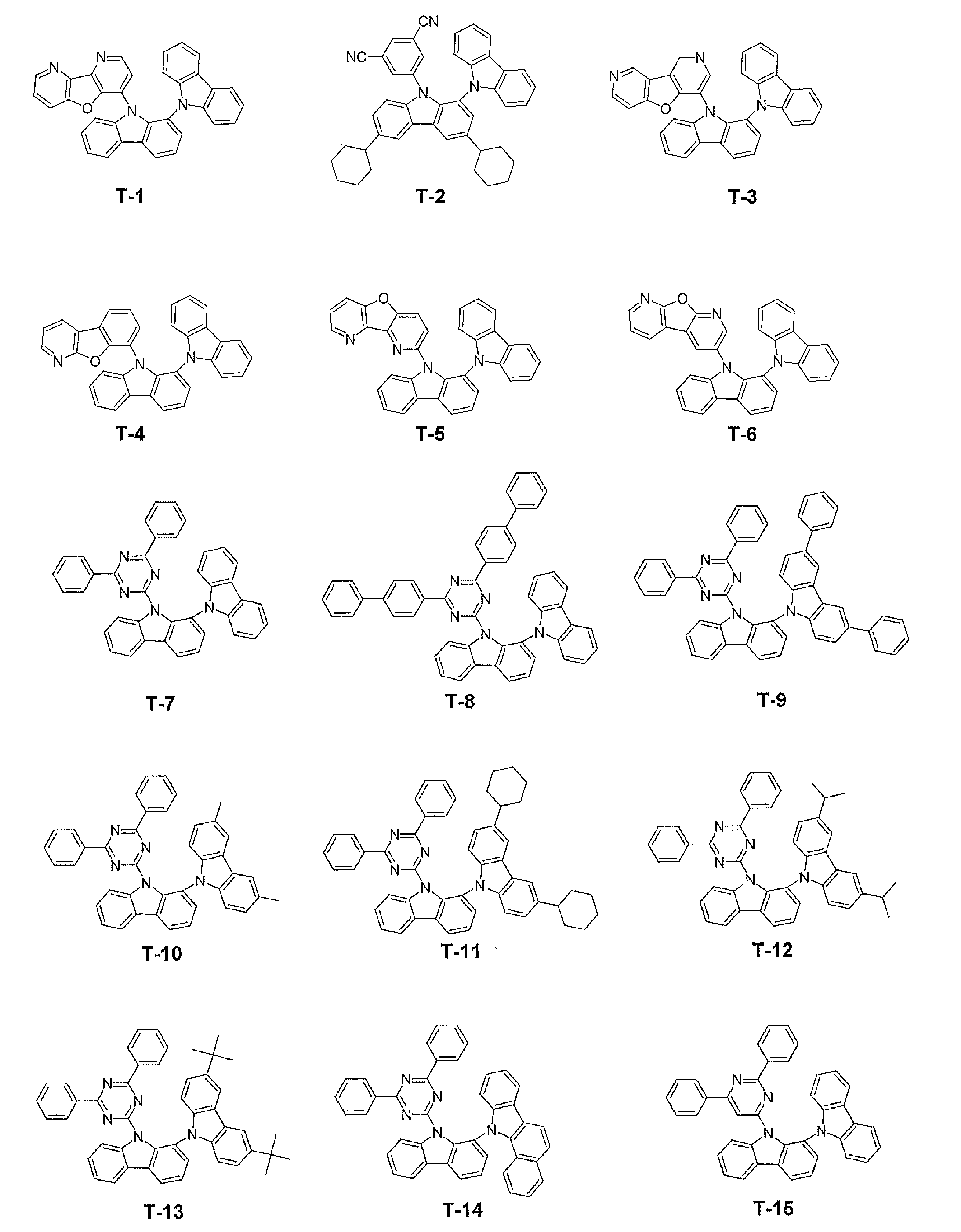
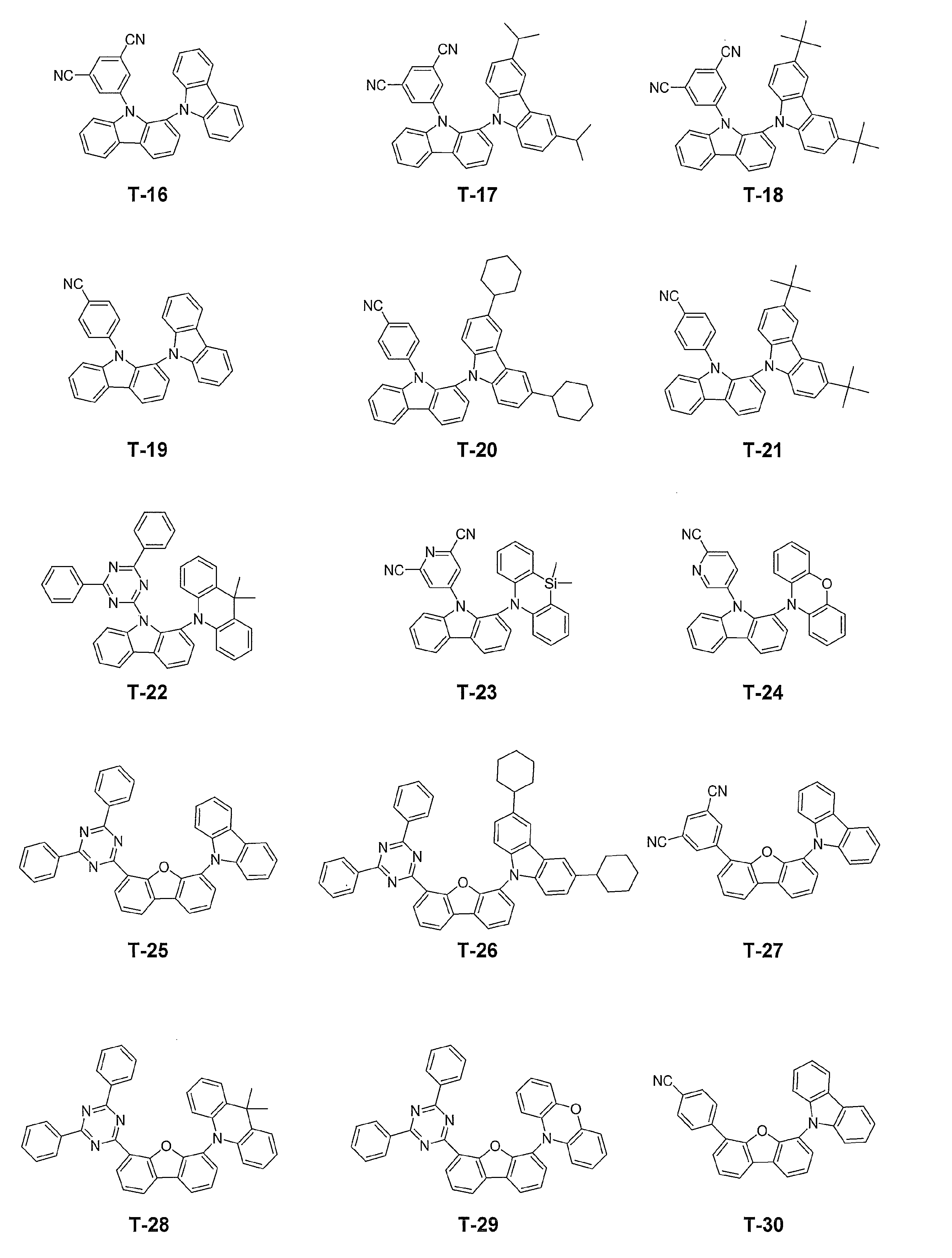

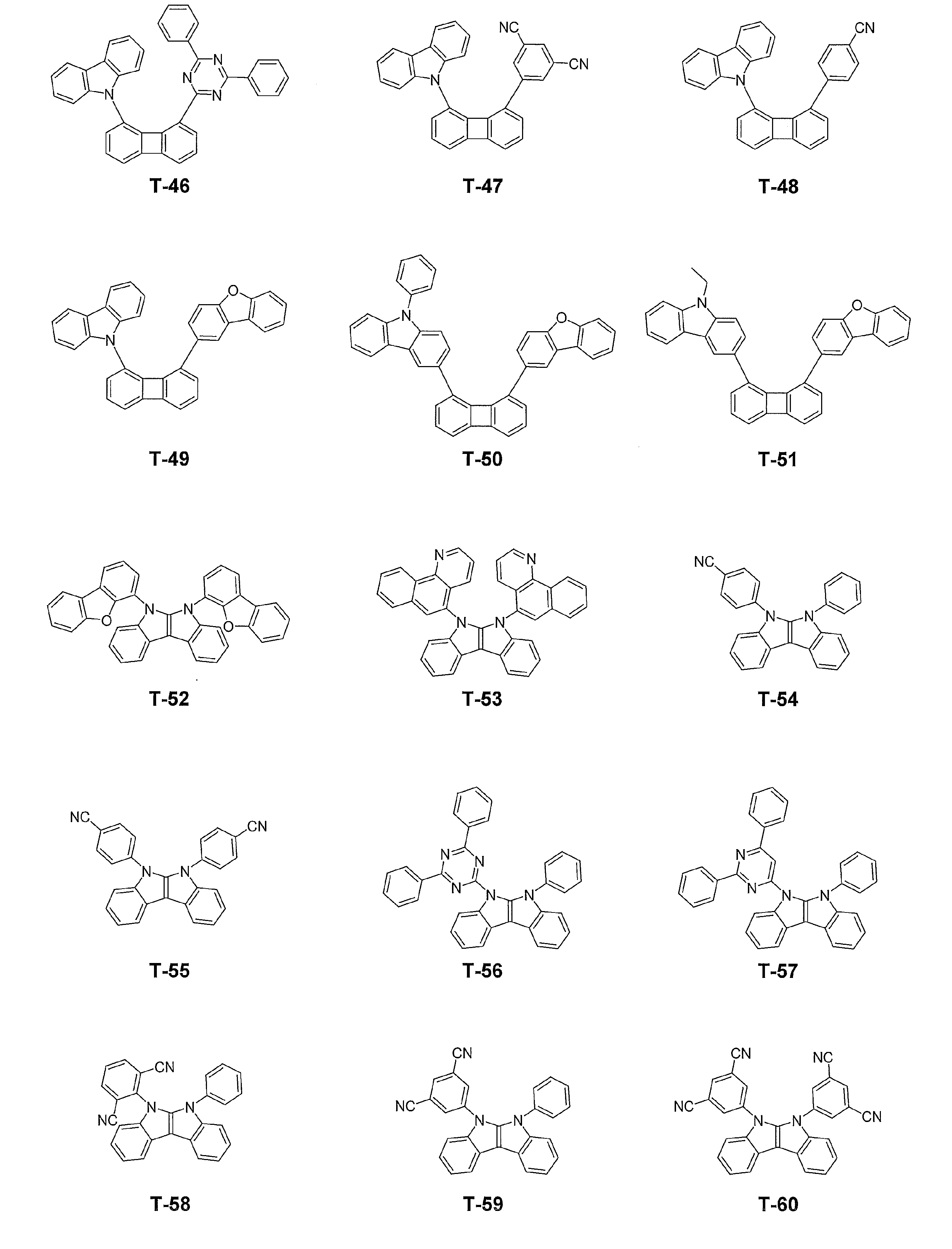
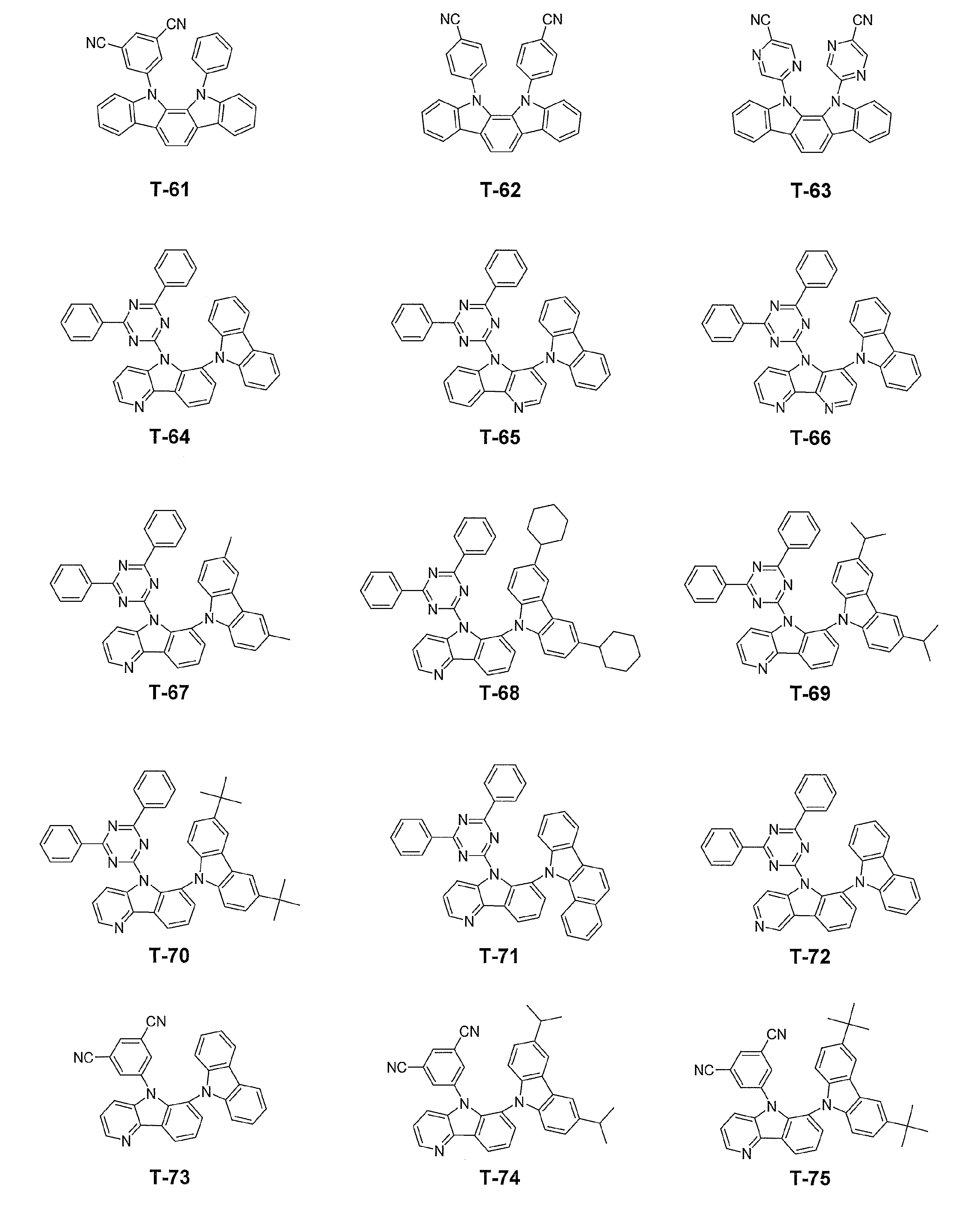

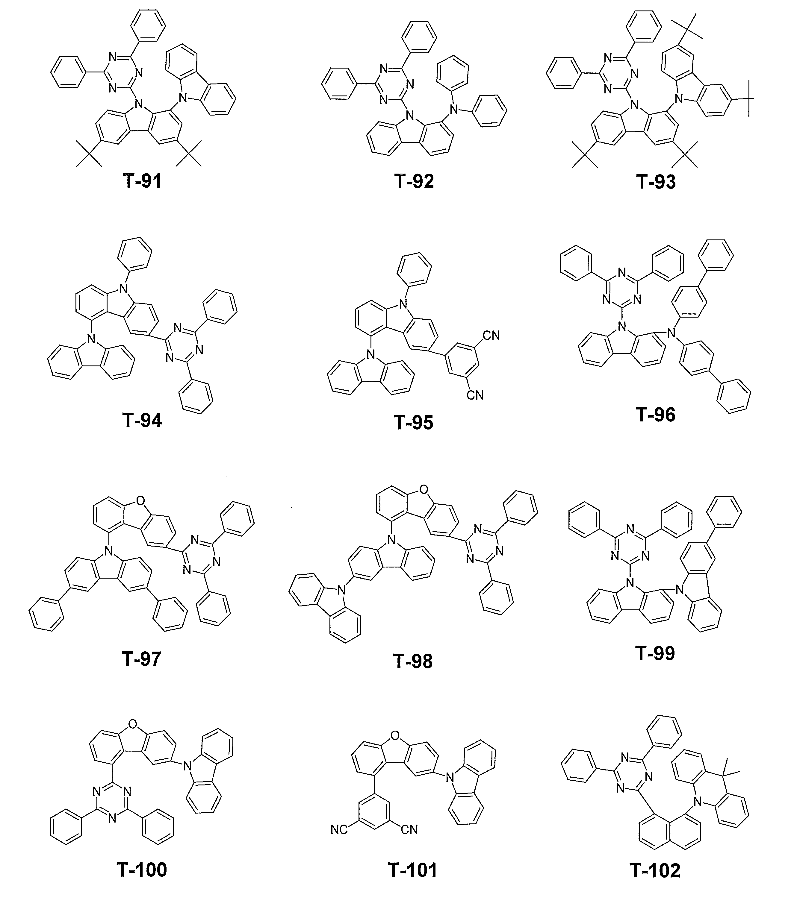
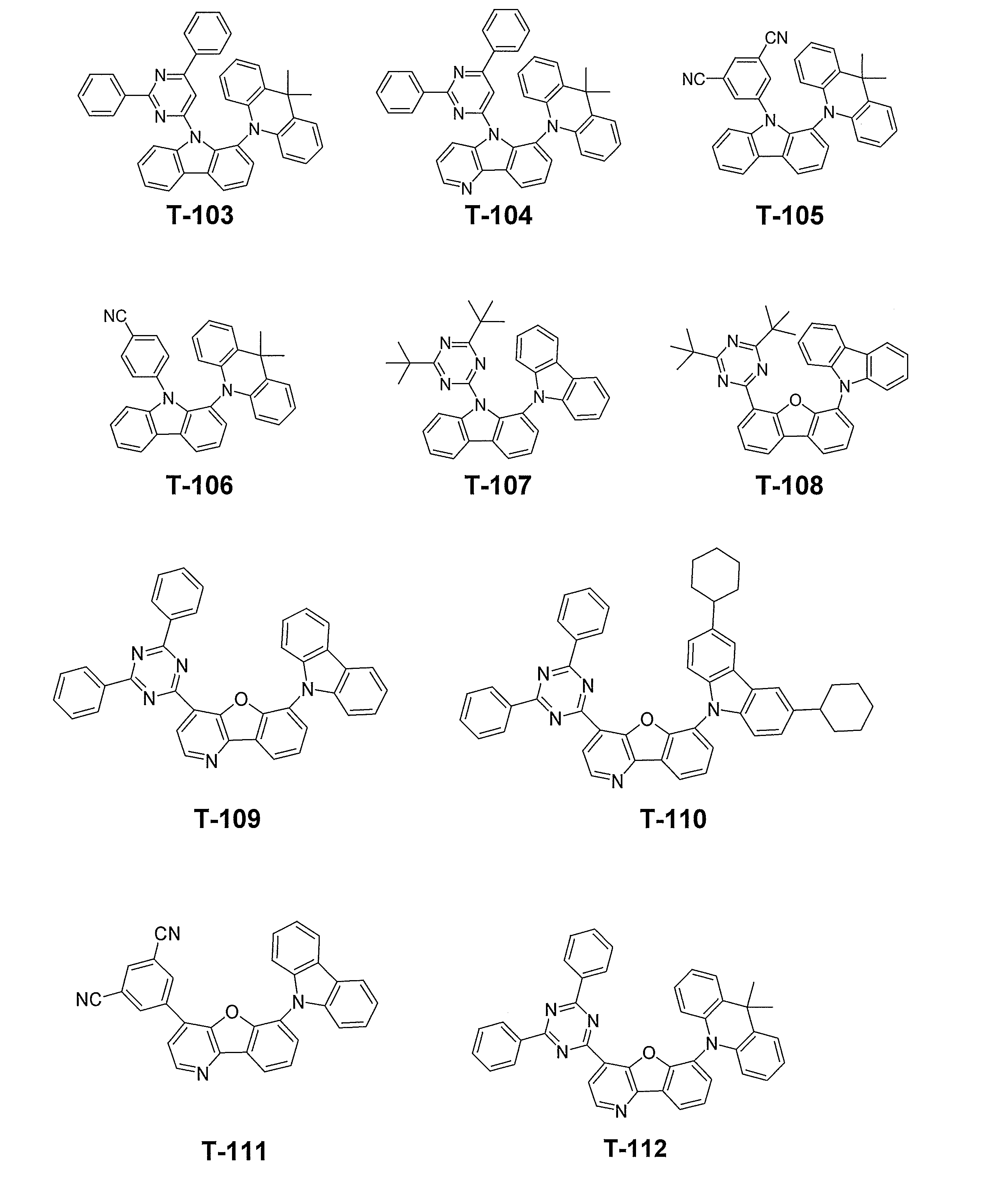
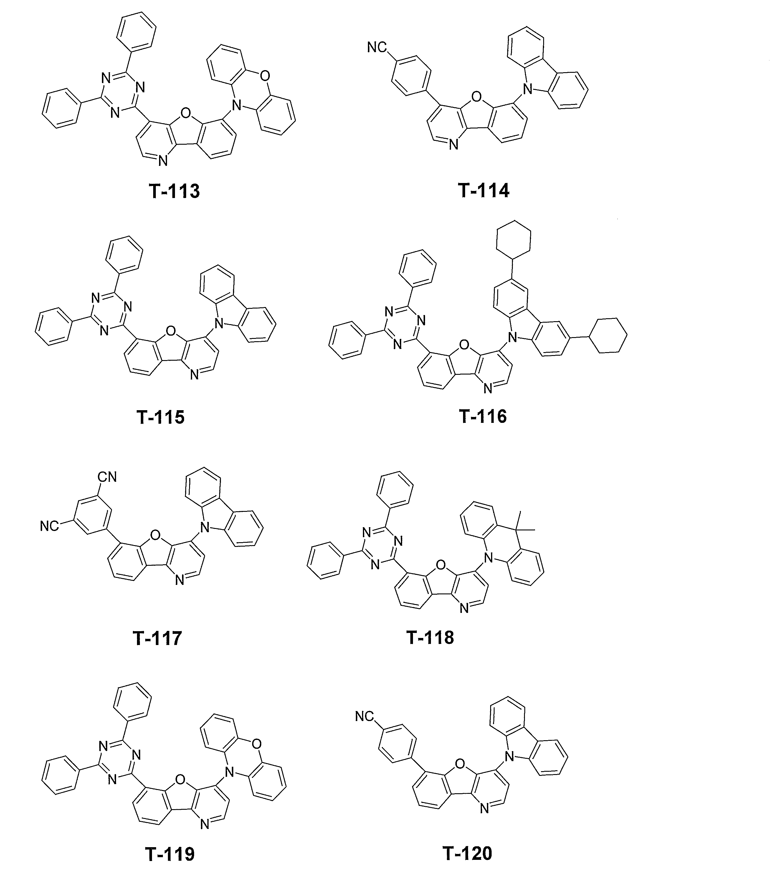
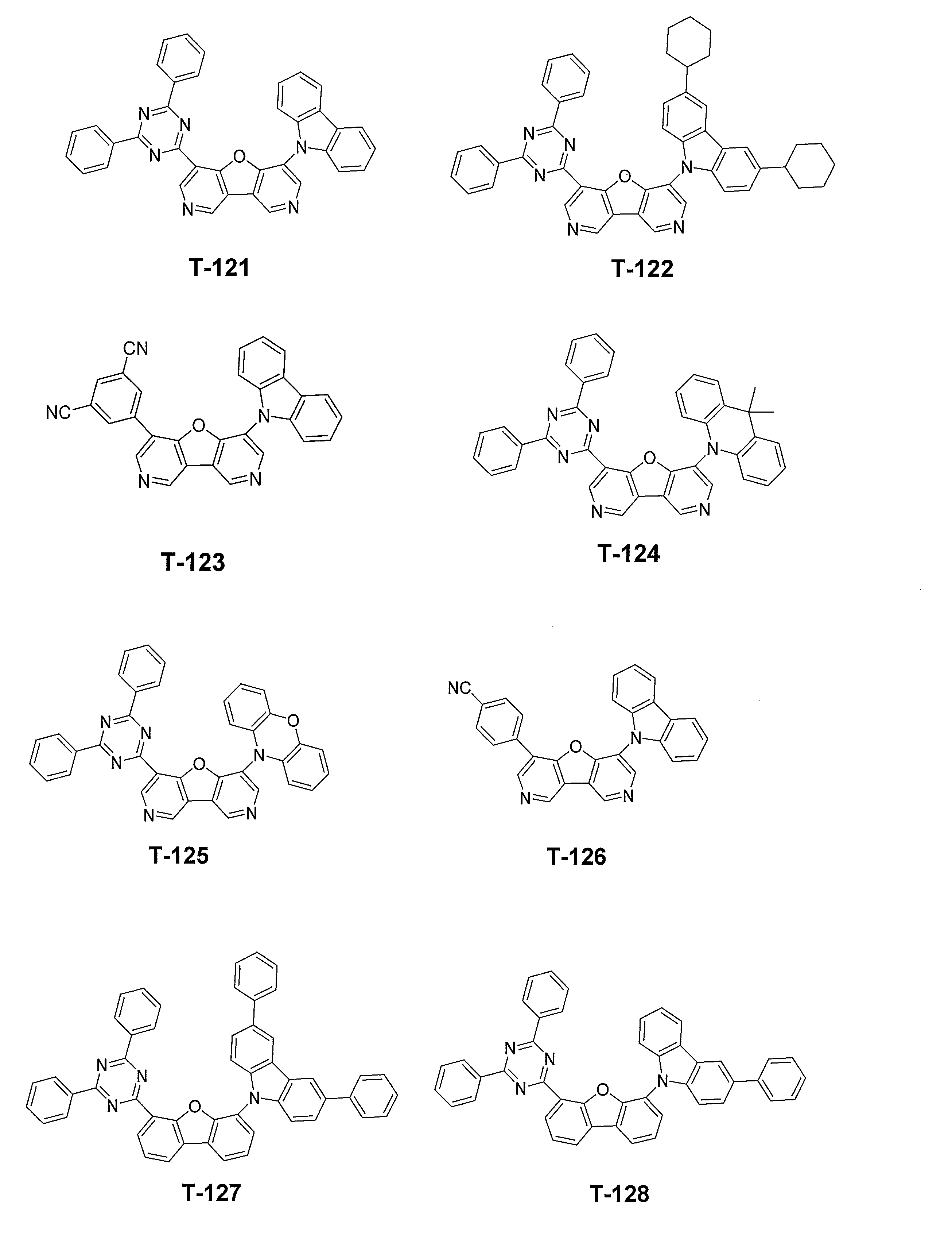
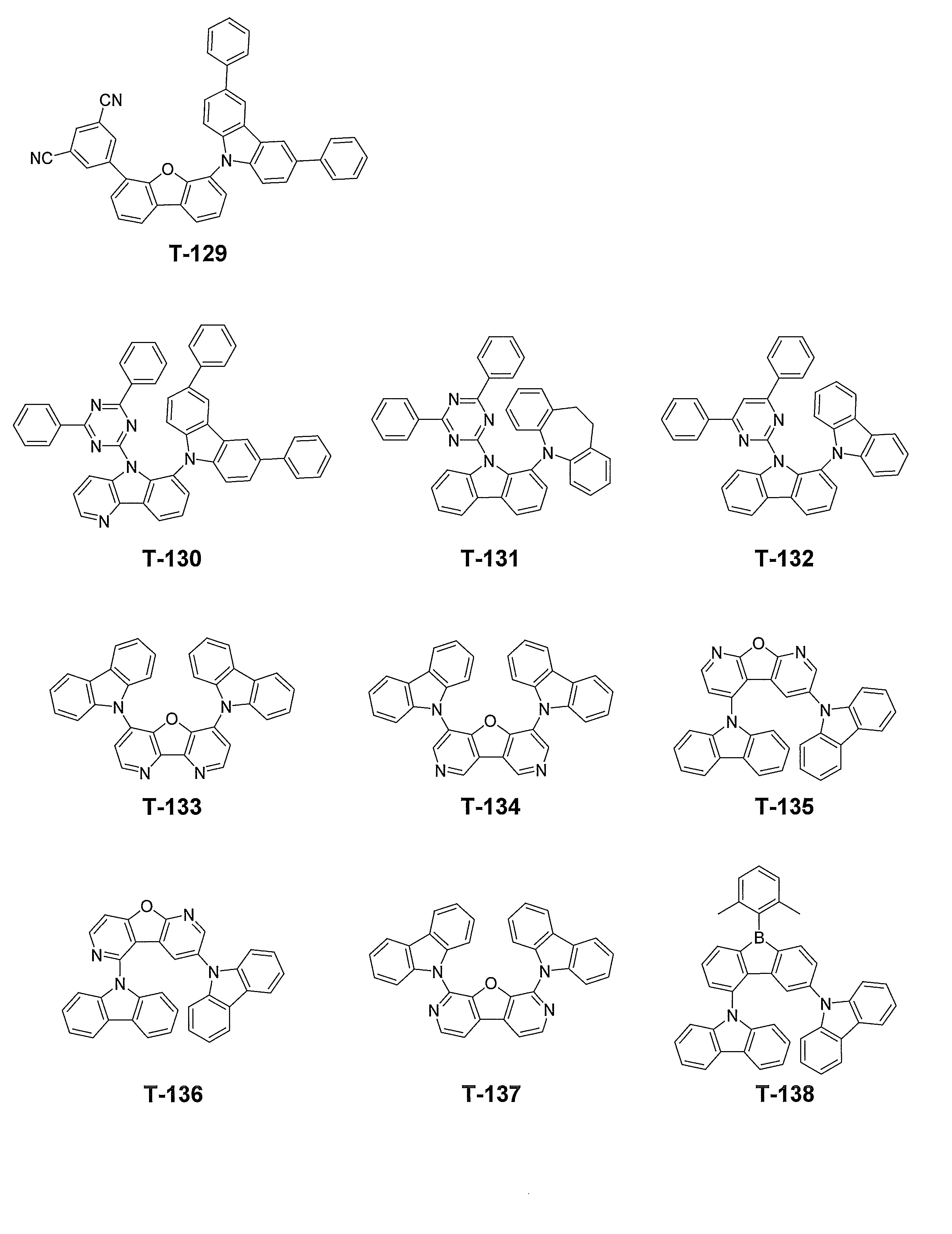

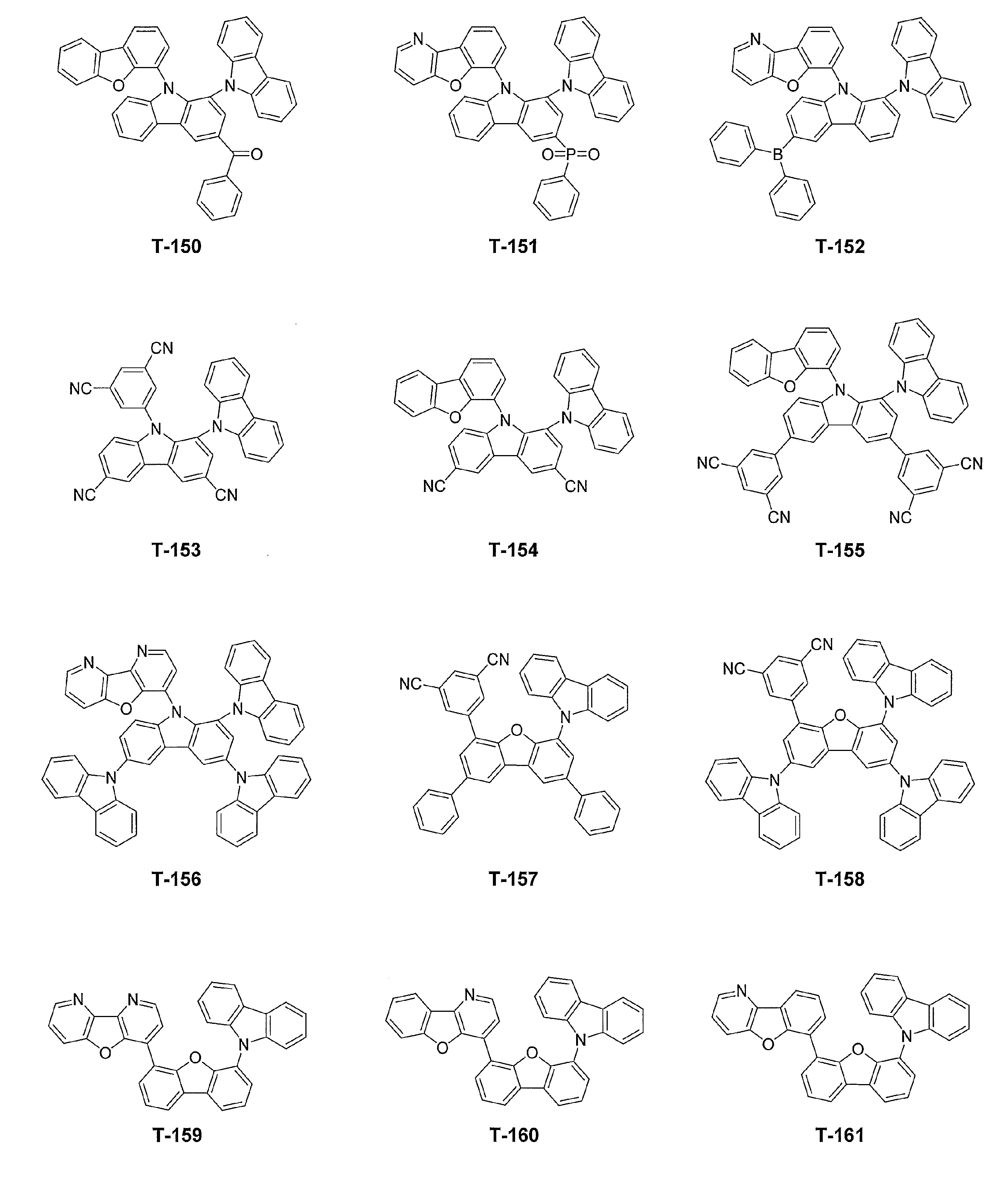
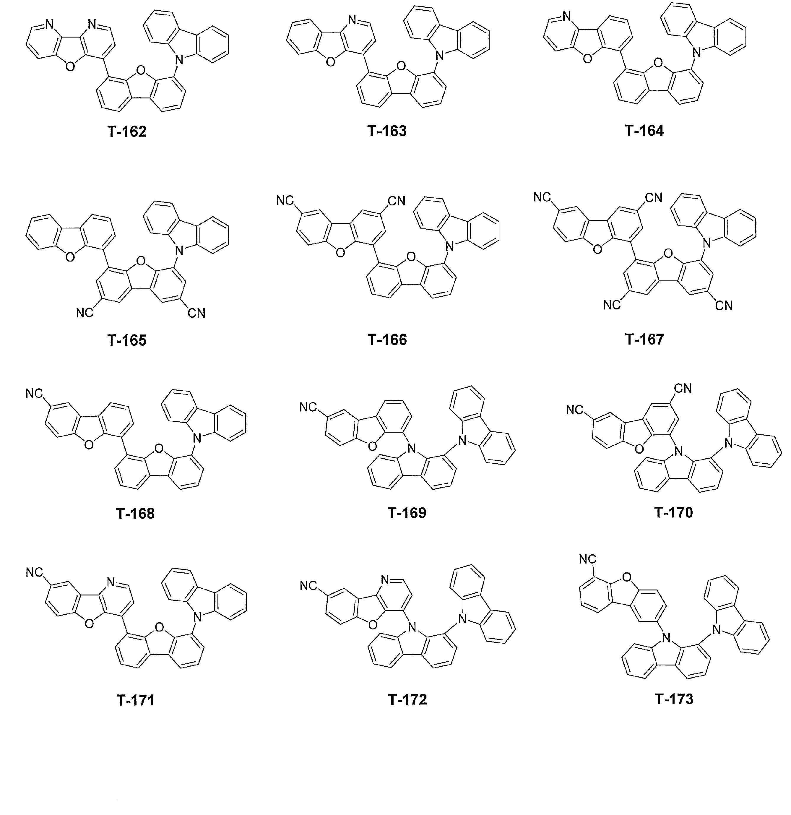

これらの化合物のうちΔESTの絶対値が0.50eV以下の材料については、TADF性(遅延蛍光性)を示す、つまり遅延蛍光を放射してもよい。ここで、遅延蛍光性を示すとは、蛍光減衰測定を行った時に、放射される蛍光の減衰速度の異なる成分が2種類以上あることをいう。なお、減衰が遅い成分は一般的には減衰時間がサブマイクロ秒以上であることが多いが、材料によって減衰時間が異なるため、減衰時間は限定されない。蛍光減衰測定は、一般的には以下のように行うことができる。π共役系化合物(発光性化合物)の溶液又は薄膜、又はπ共役系化合物と第二成分との共蒸着膜に、窒素雰囲気下で励起光を照射し、ある発光波長の光子数を計測する。そしてこのとき、放射される蛍光の減衰速度の異なる成分が2種類以上ある場合に、π共役系化合物が遅延蛍光性を示すものとする。
なお、これらの化合物は、バイポーラー性を有し、様々なエネルギー準位に対応できることから、発光材料やホスト材料としても使用できるのみならず、正孔輸送、電子輸送にも適した化合物、即ち、電荷輸送材料として使用することができるため、発光層での使用に限定されず、上述の正孔注入層、正孔輸送層、電子阻止層、正孔阻止層、電子輸送層、電子注入層、中間層などに用いてもよい。
<合成方法>
上記π共役系化合物は、例えば、国際公開第2010/113755号、Organic Letters,2002,4,1783-1785.、Angew. Chem. Int. Ed. 2010, 49, 2014-2017.に記載の方法、又は、これらの文献に記載の参照文献に記載の方法を参照することにより合成することができる。
上記π共役系化合物は、例えば、国際公開第2010/113755号、Organic Letters,2002,4,1783-1785.、Angew. Chem. Int. Ed. 2010, 49, 2014-2017.に記載の方法、又は、これらの文献に記載の参照文献に記載の方法を参照することにより合成することができる。
次に、本発明の技術思想と関連する、有機ELの発光方式及び発光材料について述べる。
<有機ELの発光方式>
有機ELの発光方式としては三重項励起状態から基底状態に戻る際に光を発する「リン光発光」と、一重項励起状態から基底状態に戻る際に光を発する「蛍光発光」の二通りがある。
有機ELのような電界で励起する場合には、三重項励起子が75%の確率で、一重項励起子が25%の確率で生成するため、リン光発光の方が蛍光発光に比べ発光効率を高くすることが可能で、低消費電力化を実現するには優れた方式である。
一方、蛍光発光においても、75%の確率で生成してしまう、通常では、励起子のエネルギーが、無輻射失活により、熱にしかならない三重項励起子を、高密度で存在させることによって、二つの三重項励起子から一つの一重項励起子を発生させて発光効率を向上させるTTA(Triplet-Triplet Annihilation、また、Triplet-Triplet Fusion:「TTF」と略記する。)機構を利用した方式が見つかっている。
有機ELの発光方式としては三重項励起状態から基底状態に戻る際に光を発する「リン光発光」と、一重項励起状態から基底状態に戻る際に光を発する「蛍光発光」の二通りがある。
有機ELのような電界で励起する場合には、三重項励起子が75%の確率で、一重項励起子が25%の確率で生成するため、リン光発光の方が蛍光発光に比べ発光効率を高くすることが可能で、低消費電力化を実現するには優れた方式である。
一方、蛍光発光においても、75%の確率で生成してしまう、通常では、励起子のエネルギーが、無輻射失活により、熱にしかならない三重項励起子を、高密度で存在させることによって、二つの三重項励起子から一つの一重項励起子を発生させて発光効率を向上させるTTA(Triplet-Triplet Annihilation、また、Triplet-Triplet Fusion:「TTF」と略記する。)機構を利用した方式が見つかっている。
さらに、近年では、安達らの発見により一重項励起状態と三重項励起状態のエネルギーギャップを小さくすることで、発光中のジュール熱及び/又は発光素子が置かれる環境温度によりエネルギー準位の低い三重項励起状態から一重項励起状態に逆項間交差がおこり、結果としてほぼ100%に近い蛍光発光を可能とする現象(熱励起型遅延蛍光又は熱励起型遅延蛍光ともいう:「TADF」)とそれを可能にする蛍光物質が見いだされている(例えば、非特許文献1等参照。)。
<リン光発光性化合物>
前述のとおり、リン光発光は発光効率的には蛍光発光よりも理論的には3倍有利であるが、三重項励起状態から一重項基底状態へのエネルギー失活(=リン光発光)は禁制遷移であり、また同様に一重項励起状態から三重項励起状態への項間交差も禁制遷移であるため、通常その速度定数は小さい。すなわち、遷移が起こりにくいため、励起子寿命はミリ秒から秒オーダーと長くなり、所望の発光を得ることが困難である。
ただし、イリジウムや白金などの重金属を用いた錯体が発光する場合には、中心金属の重原子効果によって、前記の禁制遷移の速度定数が3桁以上増大し、配位子の選択によっては、100%のリン光量子収率を得ることも可能となる。
しかしながら、このような理想的な発光を得るためには、希少金属であるイリジウムやパラジウム、白金などのいわゆる白金属と呼ばれる貴金属を用いる必要があり、大量に使用されることになるとその埋蔵量や金属自体の値段が産業上大きな問題となってくる。
前述のとおり、リン光発光は発光効率的には蛍光発光よりも理論的には3倍有利であるが、三重項励起状態から一重項基底状態へのエネルギー失活(=リン光発光)は禁制遷移であり、また同様に一重項励起状態から三重項励起状態への項間交差も禁制遷移であるため、通常その速度定数は小さい。すなわち、遷移が起こりにくいため、励起子寿命はミリ秒から秒オーダーと長くなり、所望の発光を得ることが困難である。
ただし、イリジウムや白金などの重金属を用いた錯体が発光する場合には、中心金属の重原子効果によって、前記の禁制遷移の速度定数が3桁以上増大し、配位子の選択によっては、100%のリン光量子収率を得ることも可能となる。
しかしながら、このような理想的な発光を得るためには、希少金属であるイリジウムやパラジウム、白金などのいわゆる白金属と呼ばれる貴金属を用いる必要があり、大量に使用されることになるとその埋蔵量や金属自体の値段が産業上大きな問題となってくる。
<蛍光発光性化合物>
一般的な蛍光発光性化合物は、リン光発光性化合物のような重金属錯体である必要性は特になく、炭素、酸素、窒素及び水素などの一般的な元素の組み合わせから構成される、いわゆる有機化合物が適用でき、さらに、リンや硫黄、ケイ素などその他の非金属元素を用いることも可能で、また、アルミニウムや亜鉛などの典型金属の錯体も活用できるなど、その多様性はほぼ無限と言える。
ただし、従来の蛍光化合物では前記のように励起子の25%しか発光に適用できないために、リン光発光のような高効率発光は望めない。
一般的な蛍光発光性化合物は、リン光発光性化合物のような重金属錯体である必要性は特になく、炭素、酸素、窒素及び水素などの一般的な元素の組み合わせから構成される、いわゆる有機化合物が適用でき、さらに、リンや硫黄、ケイ素などその他の非金属元素を用いることも可能で、また、アルミニウムや亜鉛などの典型金属の錯体も活用できるなど、その多様性はほぼ無限と言える。
ただし、従来の蛍光化合物では前記のように励起子の25%しか発光に適用できないために、リン光発光のような高効率発光は望めない。
<遅延蛍光化合物>
[励起三重項-三重項消滅(TTA)遅延蛍光化合物]
蛍光発光性化合物の問題点を解決すべく登場したのが遅延蛍光を利用した発光方式である。三重項励起子同士の衝突を起源とするTTA方式は、下記のような一般式で記述できる。すなわち、従来、励起子のエネルギーが、無輻射失活により、熱にしか変換されなかった三重項励起子の一部が、発光に寄与しうる一重項励起子に逆項間交差できるメリットがあり、実際の有機EL素子においても従来の蛍光発光素子の約2倍の外部取り出し量子効率を得ることができている。
一般式: T* + T* → S* + S
(式中、T*は三重項励起子、S*は一重項励起子、Sは基底状態分子を表す。)
しかしながら、上式からもわかるように、二つの三重項励起子から発光に利用できる一重項励起子は一つしか生成しないため、この方式で100%の内部量子効率を得ることは原理上できない。
[励起三重項-三重項消滅(TTA)遅延蛍光化合物]
蛍光発光性化合物の問題点を解決すべく登場したのが遅延蛍光を利用した発光方式である。三重項励起子同士の衝突を起源とするTTA方式は、下記のような一般式で記述できる。すなわち、従来、励起子のエネルギーが、無輻射失活により、熱にしか変換されなかった三重項励起子の一部が、発光に寄与しうる一重項励起子に逆項間交差できるメリットがあり、実際の有機EL素子においても従来の蛍光発光素子の約2倍の外部取り出し量子効率を得ることができている。
一般式: T* + T* → S* + S
(式中、T*は三重項励起子、S*は一重項励起子、Sは基底状態分子を表す。)
しかしながら、上式からもわかるように、二つの三重項励起子から発光に利用できる一重項励起子は一つしか生成しないため、この方式で100%の内部量子効率を得ることは原理上できない。
[熱活性型遅延蛍光(TADF)化合物]
もう一つの高効率蛍光発光であるTADF方式は、TTAの問題点を解決できる方式である。
蛍光発光性化合物は前記のごとく無限に分子設計できる利点を持っている。すなわち、分子設計された化合物の中で、特異的に三重項励起状態と一重項励起状態のエネルギー準位差が極めて近接する化合物が存在する。
このような化合物は、分子内に重原子を持っていないにもかかわらず、ΔESTが小さいために通常では起こりえない三重項励起状態から一重項励起状態への逆項間交差が起こる。さらに、一重項励起状態から基底状態への失活(=蛍光発光)の速度定数が極めて大きいことから、三重項励起子はそれ自体が基底状態に熱的に失活(無輻射失活)するよりも、一重項励起状態経由で蛍光を発しながら基底状態に戻る方が速度論的に有利である。そのため、TADFでは理論的には100%の蛍光発光が可能となる。
もう一つの高効率蛍光発光であるTADF方式は、TTAの問題点を解決できる方式である。
蛍光発光性化合物は前記のごとく無限に分子設計できる利点を持っている。すなわち、分子設計された化合物の中で、特異的に三重項励起状態と一重項励起状態のエネルギー準位差が極めて近接する化合物が存在する。
このような化合物は、分子内に重原子を持っていないにもかかわらず、ΔESTが小さいために通常では起こりえない三重項励起状態から一重項励起状態への逆項間交差が起こる。さらに、一重項励起状態から基底状態への失活(=蛍光発光)の速度定数が極めて大きいことから、三重項励起子はそれ自体が基底状態に熱的に失活(無輻射失活)するよりも、一重項励起状態経由で蛍光を発しながら基底状態に戻る方が速度論的に有利である。そのため、TADFでは理論的には100%の蛍光発光が可能となる。
<ΔESTに関する分子設計思想>
上記ΔESTを小さくするための分子設計について説明する。
ΔESTを小さくするためには、原理上分子内の最高被占軌道(Highest Occupied Molecular Orbital:HOMO)と最低空軌道(Lowest Unoccupied Molecular Orbital:LUMO)の空間的な重なりを小さくすることが最も効果的である。
一般に分子の電子軌道において、HOMOは電子供与性部位に、LUMOは電子求引性部位に分布することが知られており、分子内に電子供与性と電子求引性の骨格を導入することによって、HOMOとLUMOが存在する位置を遠ざけることが可能である。
上記ΔESTを小さくするための分子設計について説明する。
ΔESTを小さくするためには、原理上分子内の最高被占軌道(Highest Occupied Molecular Orbital:HOMO)と最低空軌道(Lowest Unoccupied Molecular Orbital:LUMO)の空間的な重なりを小さくすることが最も効果的である。
一般に分子の電子軌道において、HOMOは電子供与性部位に、LUMOは電子求引性部位に分布することが知られており、分子内に電子供与性と電子求引性の骨格を導入することによって、HOMOとLUMOが存在する位置を遠ざけることが可能である。
例えば、「実用化ステージを迎えた有機光エレクトロニクス」応用物理 第82巻、第6号、2013年においては、シアノ基やトリアジンなどの電子求引性の骨格と、カルバゾールやジフェニルアミノ基等の電子供与性の骨格とを導入することで、LUMOとHOMOとをそれぞれ局在化させている。
また、化合物の基底状態と三重項励起状態との分子構造変化を小さくすることも効果的である。構造変化を小さくするための方法としては、例えば、化合物を剛直にすることなどが効果的である。ここで述べる剛直とは、例えば、分子内の環と環との結合における自由回転を抑制することや、π共役面の大きい縮合環を導入するなど、分子内において自由に動ける部位が少ないことを意味する。特に、発光に関与する部位を剛直にすることによって、励起状態における構造変化を小さくすることが可能である。
また、化合物の基底状態と三重項励起状態との分子構造変化を小さくすることも効果的である。構造変化を小さくするための方法としては、例えば、化合物を剛直にすることなどが効果的である。ここで述べる剛直とは、例えば、分子内の環と環との結合における自由回転を抑制することや、π共役面の大きい縮合環を導入するなど、分子内において自由に動ける部位が少ないことを意味する。特に、発光に関与する部位を剛直にすることによって、励起状態における構造変化を小さくすることが可能である。
本発明のπ共役系化合物においては、電子供与性基D同士、電子求引性基A同士、又は電子供与性基Dと電子求引性基Aの間に、3~5個の原子を含み、2個又は3個の環構造を配置することで、HOMOとLUMOを分離することに成功している。本発明における特定の構造においては、電子供与性基D同士、電子求引性基A同士、又は電子供与性基Dと電子求引性基Aは、平行に近い角度で空間的に対面することが可能となるため、CT性の励起状態を効果的に形成し、安定化することができると考えられる。その結果、本願化合物の無輻射失活を抑制でき、発光効率が向上できたものと考えられる。
また、本発明のπ共役系化合物においては、電子求引性基Aや電子供与性基Dがスルーボンドでの連結ではなく、スルースペースで相互作用しているため、吸収スペクトルや発光スペクトルの長波長化も抑制できると考えられる。
以下に、本発明に係るπ共役系化合物に関する種々の測定方法について記載する。
[電子密度分布]
本発明に係るπ共役系化合物は、ΔESTを小さくするという観点から、分子内においてHOMOとLUMOが実質的に分離していることが好ましい。これらHOMO及びLUMOの分布状態については、分子軌道計算により得られる構造最適化した際の電子密度分布から求めることができる。
本発明におけるπ共役系化合物の分子軌道計算による構造最適化及び電子密度分布の算出は、計算手法として、汎関数としてB3LYP、基底関数として6-31G(d)を用いた分子軌道計算用ソフトウェアを用いて算出することができ、ソフトウェアに特に限定はなく、いずれを用いても同様に求めることができる。
本発明においては、分子軌道計算用ソフトウェアとして、米国Gaussian社製のGaussian09(Revision C.01,M.J.Frisch,et al,Gaussian,Inc.,2010.)を用いた。
本発明に係るπ共役系化合物は、ΔESTを小さくするという観点から、分子内においてHOMOとLUMOが実質的に分離していることが好ましい。これらHOMO及びLUMOの分布状態については、分子軌道計算により得られる構造最適化した際の電子密度分布から求めることができる。
本発明におけるπ共役系化合物の分子軌道計算による構造最適化及び電子密度分布の算出は、計算手法として、汎関数としてB3LYP、基底関数として6-31G(d)を用いた分子軌道計算用ソフトウェアを用いて算出することができ、ソフトウェアに特に限定はなく、いずれを用いても同様に求めることができる。
本発明においては、分子軌道計算用ソフトウェアとして、米国Gaussian社製のGaussian09(Revision C.01,M.J.Frisch,et al,Gaussian,Inc.,2010.)を用いた。
また、「HOMOとLUMOが実質的に分離している」とは、上記分子計算により算出されたHOMO軌道分布及びLUMO軌道分布の中心部位が離れており、より好ましくはHOMO軌道の分布とLUMO軌道の分布がほぼ重なっていないことを意味する。
また、HOMOとLUMOの分離状態については、前述の汎関数としてB3LYP、基底関数として6-31G(d)を用いた構造最適化計算から、さらに時間依存密度汎関数法(Time-Dependent DFT)による励起状態計算を実施してS1、T1のエネルギー準位(それぞれE(S1)、E(T1))を求めてΔEST=|E(S1)-E(T1)|として算出することも可能である。算出されたΔESTが小さいほど、HOMOとLUMOがより分離していることを示す。本発明においては、前述と同様の計算手法を用いて算出されたΔESTが0.50eV以下であり、好ましくは0.30eV以下であり、より好ましくは0.10eV以下である。
また、HOMOとLUMOの分離状態については、前述の汎関数としてB3LYP、基底関数として6-31G(d)を用いた構造最適化計算から、さらに時間依存密度汎関数法(Time-Dependent DFT)による励起状態計算を実施してS1、T1のエネルギー準位(それぞれE(S1)、E(T1))を求めてΔEST=|E(S1)-E(T1)|として算出することも可能である。算出されたΔESTが小さいほど、HOMOとLUMOがより分離していることを示す。本発明においては、前述と同様の計算手法を用いて算出されたΔESTが0.50eV以下であり、好ましくは0.30eV以下であり、より好ましくは0.10eV以下である。
[最低励起一重項エネルギー準位S1]
本発明におけるπ共役系化合物の最低励起一重項エネルギー準位S1については、本発明においても通常の手法と同様にして算出されるもので定義される。すなわち、測定対象となる化合物を石英基板上に蒸着して試料を作製し、常温(300K)でこの試料の吸収スペクトル(縦軸:吸光度、横軸:波長とする。)を測定する。この吸収スペクトルの長波長側の立ち上がりに対して接線を引き、その接線と横軸との交点の波長値に基づいて、所定の換算式から算出される。
ただし、本発明において使用するπ共役系化合物の分子自体の凝集性が比較的高い場合、薄膜の測定においては凝集による誤差を生じる可能性がある。本発明におけるπ共役系化合物はストークスシフトが比較的小さいこと、さらに励起状態と基底状態の構造変化が小さいことを考慮し、本発明における最低励起一重項エネルギー準位S1は、室温(25℃)におけるπ共役系化合物の溶液状態の最大発光波長のピーク値を近似値として用いた。
ここで、使用する溶媒は、π共役系化合物の凝集状態に影響を与えない、すなわち溶媒効果の影響が小さい溶媒、例えばシクロヘキサンやトルエン等の非極性溶媒等を用いることができる。
本発明におけるπ共役系化合物の最低励起一重項エネルギー準位S1については、本発明においても通常の手法と同様にして算出されるもので定義される。すなわち、測定対象となる化合物を石英基板上に蒸着して試料を作製し、常温(300K)でこの試料の吸収スペクトル(縦軸:吸光度、横軸:波長とする。)を測定する。この吸収スペクトルの長波長側の立ち上がりに対して接線を引き、その接線と横軸との交点の波長値に基づいて、所定の換算式から算出される。
ただし、本発明において使用するπ共役系化合物の分子自体の凝集性が比較的高い場合、薄膜の測定においては凝集による誤差を生じる可能性がある。本発明におけるπ共役系化合物はストークスシフトが比較的小さいこと、さらに励起状態と基底状態の構造変化が小さいことを考慮し、本発明における最低励起一重項エネルギー準位S1は、室温(25℃)におけるπ共役系化合物の溶液状態の最大発光波長のピーク値を近似値として用いた。
ここで、使用する溶媒は、π共役系化合物の凝集状態に影響を与えない、すなわち溶媒効果の影響が小さい溶媒、例えばシクロヘキサンやトルエン等の非極性溶媒等を用いることができる。
[最低励起三重項エネルギー準位T1]
本発明で用いられるπ共役系化合物の最低励起三重項エネルギー準位(T1)については、溶液若しくは薄膜のフォトルミネッセンス(PL)特性により算出した。例えば、薄膜における算出方法としては、希薄状態のπ共役系化合物の分散物を薄膜にした後に、ストリークカメラを用い、過渡PL特性を測定することで、蛍光成分とリン光成分の分離を行い、そのエネルギー差の絶対値をΔESTとして最低励起一重項エネルギー準位から最低励起三重項エネルギー準位を求めることができる。
測定・評価にあたって、絶対PL量子収率の測定については、絶対PL量子収率測定装置C9920-02(浜松ホトニクス社製)を用いた。発光寿命は、ストリークカメラC4334(浜松ホトニクス社製)を用いて、サンプルをレーザー光で励起させながら測定した。
本発明で用いられるπ共役系化合物の最低励起三重項エネルギー準位(T1)については、溶液若しくは薄膜のフォトルミネッセンス(PL)特性により算出した。例えば、薄膜における算出方法としては、希薄状態のπ共役系化合物の分散物を薄膜にした後に、ストリークカメラを用い、過渡PL特性を測定することで、蛍光成分とリン光成分の分離を行い、そのエネルギー差の絶対値をΔESTとして最低励起一重項エネルギー準位から最低励起三重項エネルギー準位を求めることができる。
測定・評価にあたって、絶対PL量子収率の測定については、絶対PL量子収率測定装置C9920-02(浜松ホトニクス社製)を用いた。発光寿命は、ストリークカメラC4334(浜松ホトニクス社製)を用いて、サンプルをレーザー光で励起させながら測定した。
《有機EL素子の構成層》
本発明の有機EL素子は、陽極と陰極の間に少なくとも発光層を有する有機エレクトロルミネッセンス素子であって、該発光層の少なくとも1層が、前記一般式(1)~(7)のいずれかで表される構造を有するπ共役系化合物を含有することを特徴とする。
本発明の有機EL素子における代表的な素子構成としては、以下の構成を挙げることができるが、これらに限定されるものではない。
(1)陽極/発光層/陰極
(2)陽極/発光層/電子輸送層/陰極
(3)陽極/正孔輸送層/発光層/陰極
(4)陽極/正孔輸送層/発光層/電子輸送層/陰極
(5)陽極/正孔輸送層/発光層/電子輸送層/電子注入層/陰極
(6)陽極/正孔注入層/正孔輸送層/発光層/電子輸送層/陰極
(7)陽極/正孔注入層/正孔輸送層/(電子阻止層/)発光層/(正孔阻止層/)電子輸送層/電子注入層/陰極
上記の中で(7)の構成が好ましく用いられるが、これに限定されるものではない。
本発明に用いられる発光層は、単層又は複数層で構成されており、発光層が複数の場合は各発光層の間に非発光性の中間層を設けてもよい。
本発明の有機EL素子は、陽極と陰極の間に少なくとも発光層を有する有機エレクトロルミネッセンス素子であって、該発光層の少なくとも1層が、前記一般式(1)~(7)のいずれかで表される構造を有するπ共役系化合物を含有することを特徴とする。
本発明の有機EL素子における代表的な素子構成としては、以下の構成を挙げることができるが、これらに限定されるものではない。
(1)陽極/発光層/陰極
(2)陽極/発光層/電子輸送層/陰極
(3)陽極/正孔輸送層/発光層/陰極
(4)陽極/正孔輸送層/発光層/電子輸送層/陰極
(5)陽極/正孔輸送層/発光層/電子輸送層/電子注入層/陰極
(6)陽極/正孔注入層/正孔輸送層/発光層/電子輸送層/陰極
(7)陽極/正孔注入層/正孔輸送層/(電子阻止層/)発光層/(正孔阻止層/)電子輸送層/電子注入層/陰極
上記の中で(7)の構成が好ましく用いられるが、これに限定されるものではない。
本発明に用いられる発光層は、単層又は複数層で構成されており、発光層が複数の場合は各発光層の間に非発光性の中間層を設けてもよい。
必要に応じて、発光層と陰極との間に正孔阻止層(正孔障壁層ともいう)や電子注入層(陰極バッファー層ともいう)を設けてもよく、また、発光層と陽極との間に電子阻止層(電子障壁層ともいう)や正孔注入層(陽極バッファー層ともいう)を設けてもよい。
本発明に用いられる電子輸送層とは、電子を輸送する機能を有する層であり、広い意味で電子注入層、正孔阻止層も電子輸送層に含まれる。また、複数層で構成されていてもよい。
本発明に用いられる正孔輸送層とは、正孔を輸送する機能を有する層であり、広い意味で正孔注入層、電子阻止層も正孔輸送層に含まれる。また、複数層で構成されていてもよい。
上記の代表的な素子構成において、陽極と陰極を除いた層を「有機層」ともいう。
本発明に用いられる電子輸送層とは、電子を輸送する機能を有する層であり、広い意味で電子注入層、正孔阻止層も電子輸送層に含まれる。また、複数層で構成されていてもよい。
本発明に用いられる正孔輸送層とは、正孔を輸送する機能を有する層であり、広い意味で正孔注入層、電子阻止層も正孔輸送層に含まれる。また、複数層で構成されていてもよい。
上記の代表的な素子構成において、陽極と陰極を除いた層を「有機層」ともいう。
(タンデム構造)
また、本発明の有機EL素子は、少なくとも1層の発光層を含む発光ユニットを複数積層した、いわゆるタンデム構造の素子であってもよい。
タンデム構造の代表的な素子構成としては、例えば以下の構成を挙げることができる。
陽極/第1発光ユニット/中間層/第2発光ユニット/中間層/第3発光ユニット/陰極
ここで、上記第1発光ユニット、第2発光ユニット及び第3発光ユニットは全て同じであっても、異なっていてもよい。また二つの発光ユニットが同じであり、残る一つが異なっていてもよい。
複数の発光ユニットは直接積層されていても、中間層を介して積層されていてもよく、中間層は、一般的に中間電極、中間導電層、電荷発生層、電子引抜層、接続層、中間絶縁層とも呼ばれ、陽極側の隣接層に電子を、陰極側の隣接層に正孔を供給する機能を持った層であれば、公知の材料構成を用いることができる。
また、本発明の有機EL素子は、少なくとも1層の発光層を含む発光ユニットを複数積層した、いわゆるタンデム構造の素子であってもよい。
タンデム構造の代表的な素子構成としては、例えば以下の構成を挙げることができる。
陽極/第1発光ユニット/中間層/第2発光ユニット/中間層/第3発光ユニット/陰極
ここで、上記第1発光ユニット、第2発光ユニット及び第3発光ユニットは全て同じであっても、異なっていてもよい。また二つの発光ユニットが同じであり、残る一つが異なっていてもよい。
複数の発光ユニットは直接積層されていても、中間層を介して積層されていてもよく、中間層は、一般的に中間電極、中間導電層、電荷発生層、電子引抜層、接続層、中間絶縁層とも呼ばれ、陽極側の隣接層に電子を、陰極側の隣接層に正孔を供給する機能を持った層であれば、公知の材料構成を用いることができる。
中間層に用いられる材料としては、例えば、ITO(インジウムスズ酸化物)、IZO(インジウム・亜鉛酸化物)、ZnO2、TiN、ZrN、HfN、TiOx、VOx、CuI、InN、GaN、CuAlO2、CuGaO2、SrCu2O2、LaB6、RuO2、Al等の導電性無機化合物層や、Au/Bi2O3等の2層膜や、SnO2/Ag/SnO2、ZnO/Ag/ZnO、Bi2O3/Au/Bi2O3、TiO2/TiN/TiO2、TiO2/ZrN/TiO2等の多層膜、またC60等のフラーレン類、オリゴチオフェン等の導電性有機物層、金属フタロシアニン類、無金属フタロシアニン類、金属ポルフィリン類、無金属ポルフィリン類等の導電性有機化合物層等が挙げられるが、本発明はこれらに限定されない。
発光ユニット内の好ましい構成としては、例えば、上記の代表的な素子構成で挙げた(1)~(7)の構成から、陽極と陰極を除いたもの等が挙げられるが、本発明はこれらに限定されない。
発光ユニット内の好ましい構成としては、例えば、上記の代表的な素子構成で挙げた(1)~(7)の構成から、陽極と陰極を除いたもの等が挙げられるが、本発明はこれらに限定されない。
タンデム型有機EL素子の具体例としては、例えば、米国特許第6337492号明細書、米国特許第7420203号明細書、米国特許第7473923号明細書、米国特許第6872472号明細書、米国特許第6107734号明細書、米国特許第6337492号明細書、国際公開第2005/009087号、特開2006-228712号公報、特開2006-24791号公報、特開2006-49393号公報、特開2006-49394号公報、特開2006-49396号公報、特開2011-96679号公報、特開2005-340187号公報、特許第4711424号公報、特許第3496681号公報、特許第3884564号公報、特許第4213169号公報、特開2010-192719号公報、特開2009-076929号公報、特開2008-078414号公報、特開2007-059848号公報、特開2003-272860号公報、特開2003-045676号公報、国際公開第2005/094130号等に記載の素子構成や構成材料等が挙げられるが、本発明はこれらに限定されない。
以下、本発明の有機EL素子を構成する各層について説明する。
《発光層》
本発明に用いられる発光層は、電極又は隣接層から注入されてくる電子及び正孔が再結合し、励起子を経由して発光する場を提供する層であり、発光する部分は発光層の層内であっても、発光層と隣接層との界面であってもよい。本発明に用いられる発光層は、本発明で規定する要件を満たしていれば、その構成に特に制限はない。
発光層の層厚の総和は、特に制限はないが、形成する膜の均質性や、発光時に不必要な高電圧を印加するのを防止し、かつ、駆動電流に対する発光色の安定性向上の観点から、2nm~5μmの範囲に調整することが好ましく、より好ましくは2~500nmの範囲に調整され、更に好ましくは5~200nmの範囲に調整される。
また、本発明に用いられる個々の発光層の層厚としては、2nm~1μmの範囲に調整することが好ましく、より好ましくは2~200nmの範囲に調整され、更に好ましくは3~150nmの範囲に調整される。
本発明に用いられる発光層は、一層で構成されてもよいし、複数の層から構成されてもよい。本願のπ共役系化合物を発光層に用いる場合、単独で用いてもよいし、後述のホスト材料、蛍光発光材料、りん光発光材料などと混合して用いてもよい。発光層の少なくとも一層が、発光ドーパント(発光性化合物、発光性ドーパント、単にドーパントともいう。)を含有し、さらにホスト化合物(マトリックス材料、発光ホスト化合物、単にホスト、ともいう。)を含有することが好ましい。本願のπ共役系化合物は、発光層の少なくとも一層が、本願π共役系化合物と、ホスト化合物とを含有すると、発光効率が向上するため好ましい。発光層の少なくとも一層が、本願π共役系化合物と、蛍光発光性化合物及びリン光発光性化合物のうち少なくとも1種類とを含有すると、発光効率が向上するため好ましい。発光層の少なくとも一層が、本願π共役系化合物と、蛍光発光性化合物及びリン光発光性化合物のうち少なくとも1種類と、ホスト化合物とを含有すると、発光効率が向上するため好ましい。
本発明に用いられる発光層は、電極又は隣接層から注入されてくる電子及び正孔が再結合し、励起子を経由して発光する場を提供する層であり、発光する部分は発光層の層内であっても、発光層と隣接層との界面であってもよい。本発明に用いられる発光層は、本発明で規定する要件を満たしていれば、その構成に特に制限はない。
発光層の層厚の総和は、特に制限はないが、形成する膜の均質性や、発光時に不必要な高電圧を印加するのを防止し、かつ、駆動電流に対する発光色の安定性向上の観点から、2nm~5μmの範囲に調整することが好ましく、より好ましくは2~500nmの範囲に調整され、更に好ましくは5~200nmの範囲に調整される。
また、本発明に用いられる個々の発光層の層厚としては、2nm~1μmの範囲に調整することが好ましく、より好ましくは2~200nmの範囲に調整され、更に好ましくは3~150nmの範囲に調整される。
本発明に用いられる発光層は、一層で構成されてもよいし、複数の層から構成されてもよい。本願のπ共役系化合物を発光層に用いる場合、単独で用いてもよいし、後述のホスト材料、蛍光発光材料、りん光発光材料などと混合して用いてもよい。発光層の少なくとも一層が、発光ドーパント(発光性化合物、発光性ドーパント、単にドーパントともいう。)を含有し、さらにホスト化合物(マトリックス材料、発光ホスト化合物、単にホスト、ともいう。)を含有することが好ましい。本願のπ共役系化合物は、発光層の少なくとも一層が、本願π共役系化合物と、ホスト化合物とを含有すると、発光効率が向上するため好ましい。発光層の少なくとも一層が、本願π共役系化合物と、蛍光発光性化合物及びリン光発光性化合物のうち少なくとも1種類とを含有すると、発光効率が向上するため好ましい。発光層の少なくとも一層が、本願π共役系化合物と、蛍光発光性化合物及びリン光発光性化合物のうち少なくとも1種類と、ホスト化合物とを含有すると、発光効率が向上するため好ましい。
(1)発光ドーパント
発光ドーパントとしては、蛍光発光性ドーパント(蛍光発光性化合物、蛍光ドーパントともいう。)と、リン光発光性ドーパント(リン光発光性化合物、リン光ドーパントともいう。)が好ましく用いられる。本発明においては、発光層が、本発明に係るπ共役系化合物を蛍光発光性化合物又はアシストドーパントとして、0.1~50質量%の範囲内で含有し、特に、1~30質量%の範囲内で含有することが好ましい。
発光ドーパントとしては、蛍光発光性ドーパント(蛍光発光性化合物、蛍光ドーパントともいう。)と、リン光発光性ドーパント(リン光発光性化合物、リン光ドーパントともいう。)が好ましく用いられる。本発明においては、発光層が、本発明に係るπ共役系化合物を蛍光発光性化合物又はアシストドーパントとして、0.1~50質量%の範囲内で含有し、特に、1~30質量%の範囲内で含有することが好ましい。
本発明においては、発光層が発光性化合物を0.1~50質量%の範囲内で含有し、特に、1~30質量%の範囲内で含有することが好ましい。
発光層中の発光性化合物の濃度については、使用される特定の発光性化合物及びデバイスの必要条件に基づいて、任意に決定することができ、発光層の層厚方向に対し、均一な濃度で含有されていてもよく、また任意の濃度分布を有していてもよい。
また、本発明で用いられる発光性化合物は、複数種を併用して用いてもよく、構造の異なる蛍光発光性化合物同士の組み合わせや、蛍光発光性化合物とリン光発光性化合物とを組み合わせて用いてもよい。これにより、任意の発光色を得ることができる。
発光層中の発光性化合物の濃度については、使用される特定の発光性化合物及びデバイスの必要条件に基づいて、任意に決定することができ、発光層の層厚方向に対し、均一な濃度で含有されていてもよく、また任意の濃度分布を有していてもよい。
また、本発明で用いられる発光性化合物は、複数種を併用して用いてもよく、構造の異なる蛍光発光性化合物同士の組み合わせや、蛍光発光性化合物とリン光発光性化合物とを組み合わせて用いてもよい。これにより、任意の発光色を得ることができる。
最低励起一重項エネルギー準位と最低励起三重項エネルギー準位の差の絶対値(ΔEST)が、0.50eV以下である本発明に係るπ共役系化合物と、発光性化合物と、ホスト化合物を発光層に含有する場合、本発明に係るπ共役系化合物はアシストドーパントとして作用する。一方、発光層が、本発明に係るπ共役系化合物と発光性化合物を含有し、ホスト化合物を含有しない場合、本発明に係るπ共役系化合物はホスト化合物として作用する。発光層が、本発明に係るπ共役系化合物のみを含有する場合、本発明に係るπ共役系化合物はホスト化合物兼発光性化合物として作用する。
効果が発現する機構としては、いずれの場合も同様であり、本発明に係るπ共役系化合物上に生成した三重項励起子を逆項間交差(RISC)で一重項励起子へと変換する点にある。
これにより、本発明に係るπ共役系化合物上に生成した理論上すべての励起子エネルギーを発光性化合物に蛍光共鳴エネルギー移動(FRET)することができ、高発光効率の発現を可能にする。
したがって、発光層が、本発明に係るπ共役系化合物、発光性化合物及びホスト化合物の3成分を含有する場合は、π共役系化合物のS1とT1のエネルギー準位は、ホスト化合物のS1とT1のエネルギー準位よりも低く、発光性化合物のS1とT1のエネルギー準位よりも高い方が好ましい。
同様に、発光層が、本発明に係るπ共役系化合物と発光性化合物の2成分を含有する場合は、π共役系化合物のS1とT1のエネルギー準位は、発光性化合物のS1とT1のエネルギー準位よりも高い方が好ましい。
効果が発現する機構としては、いずれの場合も同様であり、本発明に係るπ共役系化合物上に生成した三重項励起子を逆項間交差(RISC)で一重項励起子へと変換する点にある。
これにより、本発明に係るπ共役系化合物上に生成した理論上すべての励起子エネルギーを発光性化合物に蛍光共鳴エネルギー移動(FRET)することができ、高発光効率の発現を可能にする。
したがって、発光層が、本発明に係るπ共役系化合物、発光性化合物及びホスト化合物の3成分を含有する場合は、π共役系化合物のS1とT1のエネルギー準位は、ホスト化合物のS1とT1のエネルギー準位よりも低く、発光性化合物のS1とT1のエネルギー準位よりも高い方が好ましい。
同様に、発光層が、本発明に係るπ共役系化合物と発光性化合物の2成分を含有する場合は、π共役系化合物のS1とT1のエネルギー準位は、発光性化合物のS1とT1のエネルギー準位よりも高い方が好ましい。
図3及び図4に、本発明のπ共役系化合物がそれぞれアシストドーパント及びホスト化合物として作用する場合の模式図を示す。図3及び図4は一例であって、本発明に係るπ共役系化合物上に生成する三重項励起子の生成過程は電界励起のみに限定されず、発光層内又は周辺層界面からのエネルギー移動や電子移動等も含まれる。
さらに、図3及び図4では、発光材料として蛍光発光性化合物を用いて示しているが、これに限定されず、リン光発光性化合物を用いてもよいし、蛍光発光性化合物とリン光発光性化合物の両者を用いてもよい。
さらに、図3及び図4では、発光材料として蛍光発光性化合物を用いて示しているが、これに限定されず、リン光発光性化合物を用いてもよいし、蛍光発光性化合物とリン光発光性化合物の両者を用いてもよい。
本発明に係るπ共役系化合物をアシストドーパントとして用いる場合、発光層は、π共役系化合物に対し質量比で100%以上のホスト化合物を含有し、蛍光発光性化合物及び/又はリン光発光性化合物がπ共役系化合物に対して質量比0.1~50%の範囲内で含有していることが好ましい。
本発明に係るπ共役系化合物をホスト化合物として用いる場合、発光層は、蛍光発光性化合物及び/又はリン光発光性化合物をπ共役系化合物に対して質量比0.1~50%の範囲内で含有することが好ましい。
本発明に係るπ共役系化合物をアシストドーパント又はホスト化合物として用いる場合、本発明に係るπ共役系化合物の発光スペクトルと発光性化合物の吸収スペクトルが重なることが好ましい。
本発明の有機EL素子や本発明に用いられる化合物の発光する色は、「新編色彩科学ハンドブック」(日本色彩学会編、東京大学出版会、1985)の108頁の図3.16において、分光放射輝度計CS-1000(コニカミノルタ(株)製)で測定した結果をCIE色度座標に当てはめたときの色で決定される。
本発明においては、1層又は複数層の発光層が、発光色の異なる複数の発光ドーパントを含有し、白色発光を示すことも好ましい。
白色を示す発光ドーパントの組み合わせについては特に限定はないが、例えば青と橙や、青と緑と赤の組合わせ等が挙げられる。
本発明の有機EL素子における白色とは、2度視野角正面輝度を前述の方法により測定した際に、1000cd/m2でのCIE1931表色系における色度がx=0.39±0.09、y=0.38±0.08の領域内にあることが好ましい。
本発明においては、1層又は複数層の発光層が、発光色の異なる複数の発光ドーパントを含有し、白色発光を示すことも好ましい。
白色を示す発光ドーパントの組み合わせについては特に限定はないが、例えば青と橙や、青と緑と赤の組合わせ等が挙げられる。
本発明の有機EL素子における白色とは、2度視野角正面輝度を前述の方法により測定した際に、1000cd/m2でのCIE1931表色系における色度がx=0.39±0.09、y=0.38±0.08の領域内にあることが好ましい。
(1.1)蛍光発光性ドーパント
蛍光発光性ドーパント(蛍光ドーパント)は、本発明のπ共役系化合物を用いてもよいし、有機EL素子の発光層に使用される公知の蛍光ドーパントや遅延蛍光性ドーパントの中から適宜選択して用いてもよい。
蛍光発光性ドーパント(蛍光ドーパント)は、本発明のπ共役系化合物を用いてもよいし、有機EL素子の発光層に使用される公知の蛍光ドーパントや遅延蛍光性ドーパントの中から適宜選択して用いてもよい。
本発明に使用できる公知の蛍光ドーパントの具体例としては、例えば、アントラセン誘導体、ピレン誘導体、クリセン誘導体、フルオランテン誘導体、ペリレン誘導体、フルオレン誘導体、アリールアセチレン誘導体、スチリルアリーレン誘導体、スチリルアミン誘導体、アリールアミン誘導体、ホウ素錯体、クマリン誘導体、ピラン誘導体、シアニン誘導体、クロコニウム誘導体、スクアリウム誘導体、オキソベンツアントラセン誘導体、フルオレセイン誘導体、ローダミン誘導体、ピリリウム誘導体、ペリレン誘導体、ポリチオフェン誘導体、又は希土類錯体系化合物等が挙げられる。また、近年では遅延蛍光を利用した発光ドーパントも開発されており、これらを用いてもよい。遅延蛍光を利用した発光ドーパントの具体例としては、例えば、国際公開第2011/156793号、特開2011-213643号公報、特開2010-93181号公報、特許5366106号公報等に記載の化合物が挙げられるが、本発明はこれらに限定されない。
(1.2)リン光発光性ドーパント
本発明に用いられるリン光発光性ドーパントについて説明する。
本発明に用いられるリン光発光性ドーパントは、励起三重項からの発光が観測される化合物であり、具体的には、室温(25℃)にてリン光発光する化合物であり、リン光量子収率が、25℃において0.01以上の化合物であると定義されるが、好ましいリン光量子収率は0.1以上である。
上記リン光量子収率は、第4版実験化学講座7の分光IIの398頁(1992年版、丸善)に記載の方法により測定できる。溶液中でのリン光量子収率は種々の溶媒を用いて測定できるが、本発明に用いられるリン光ドーパントは、任意の溶媒のいずれかにおいて上記リン光量子収率(0.01以上)が達成されればよい。
本発明に用いられるリン光発光性ドーパントについて説明する。
本発明に用いられるリン光発光性ドーパントは、励起三重項からの発光が観測される化合物であり、具体的には、室温(25℃)にてリン光発光する化合物であり、リン光量子収率が、25℃において0.01以上の化合物であると定義されるが、好ましいリン光量子収率は0.1以上である。
上記リン光量子収率は、第4版実験化学講座7の分光IIの398頁(1992年版、丸善)に記載の方法により測定できる。溶液中でのリン光量子収率は種々の溶媒を用いて測定できるが、本発明に用いられるリン光ドーパントは、任意の溶媒のいずれかにおいて上記リン光量子収率(0.01以上)が達成されればよい。
リン光ドーパントは、有機EL素子の発光層に使用される公知のものの中から適宜選択して用いることができる。本発明に使用できる公知のリン光ドーパントの具体例としては、以下の文献に記載されている化合物等が挙げられる。
Nature 395,151(1998)、Appl.Phys.Lett.78,1622(2001)、Adv.Mater.19,739(2007)、Chem.Mater.17,3532(2005)、Adv.Mater.17,1059(2005)、国際公開第2009/100991号、国際公開第2008/101842号、国際公開第2003/040257号、米国特許出願公開第2006/835469号明細書、米国特許出願公開第2006/0202194号明細書、米国特許出願公開第2007/0087321号明細書、米国特許出願公開第2005/0244673号明細書、Inorg.Chem.40,1704(2001)、Chem.Mater.16,2480(2004)、Adv.Mater.16,2003(2004)、Angew.Chem.lnt.Ed.2006,45,7800、Appl.Phys.Lett.86,153505(2005)、Chem.Lett.34,592(2005)、Chem.Commun.2906(2005)、Inorg.Chem.42,1248(2003)、国際公開第2009/050290号、国際公開第2002/015645号、国際公開第2009/000673号、米国特許出願公開第2002/0034656号明細書、米国特許第7332232号明細書、米国特許出願公開第2009/0108737号明細書、米国特許出願公開第2009/0039776号明細書、米国特許第6921915号明細書、米国特許第6687266号明細書、米国特許出願公開第2007/0190359号明細書、米国特許出願公開第2006/0008670号明細書、米国特許出願公開第2009/0165846号明細書、米国特許出願公開第2008/0015355号明細書、米国特許第7250226号明細書、米国特許第7396598号明細書、米国特許出願公開第2006/0263635号明細書、米国特許出願公開第2003/0138657号明細書、米国特許出願公開第2003/0152802号明細書、米国特許第7090928号明細書、Angew.Chem.lnt.Ed.47,1(2008)、Chem.Mater.18,5119(2006)、Inorg.Chem.46,4308(2007)、Organometallics 23,3745(2004)、Appl.Phys.Lett.74,1361(1999)、国際公開第2002/002714号、国際公開第2006/009024号、国際公開第2006/056418号、国際公開第2005/019373号、国際公開第2005/123873号、国際公開第2005/123873号、国際公開第2007/004380号、国際公開第2006/082742号、米国特許出願公開第2006/0251923号明細書、米国特許出願公開第2005/0260441号明細書、米国特許第7393599号明細書、米国特許第7534505号明細書、米国特許第7445855号明細書、米国特許出願公開第2007/0190359号明細書、米国特許出願公開第2008/0297033号明細書、米国特許第7338722号明細書、米国特許出願公開第2002/0134984号明細書、米国特許第7279704号明細書、米国特許出願公開第2006/098120号明細書、米国特許出願公開第2006/103874号明細書、国際公開第2005/076380号、国際公開第2010/032663号、国際公開第2008/140115号、国際公開第2007/052431号、国際公開第2011/134013号、国際公開第2011/157339号、国際公開第2010/086089号、国際公開第2009/113646号、国際公開第2012/020327号、国際公開第2011/051404号、国際公開第2011/004639号、国際公開第2011/073149号、米国特許出願公開第2012/228583号明細書、米国特許出願公開第2012/212126号明細書、特開2012-069737号公報、特願2011-181303号公報、特開2009-114086号公報、特開2003-81988号公報、特開2002-302671号公報、特開2002-363552号公報等である。
中でも、好ましいリン光ドーパントとしてはIrを中心金属に有する有機金属錯体が挙げられる。さらに好ましくは、金属-炭素結合、金属-窒素結合、金属-酸素結合、金属-硫黄結合の少なくとも一つの配位様式を含む錯体が好ましい。
Nature 395,151(1998)、Appl.Phys.Lett.78,1622(2001)、Adv.Mater.19,739(2007)、Chem.Mater.17,3532(2005)、Adv.Mater.17,1059(2005)、国際公開第2009/100991号、国際公開第2008/101842号、国際公開第2003/040257号、米国特許出願公開第2006/835469号明細書、米国特許出願公開第2006/0202194号明細書、米国特許出願公開第2007/0087321号明細書、米国特許出願公開第2005/0244673号明細書、Inorg.Chem.40,1704(2001)、Chem.Mater.16,2480(2004)、Adv.Mater.16,2003(2004)、Angew.Chem.lnt.Ed.2006,45,7800、Appl.Phys.Lett.86,153505(2005)、Chem.Lett.34,592(2005)、Chem.Commun.2906(2005)、Inorg.Chem.42,1248(2003)、国際公開第2009/050290号、国際公開第2002/015645号、国際公開第2009/000673号、米国特許出願公開第2002/0034656号明細書、米国特許第7332232号明細書、米国特許出願公開第2009/0108737号明細書、米国特許出願公開第2009/0039776号明細書、米国特許第6921915号明細書、米国特許第6687266号明細書、米国特許出願公開第2007/0190359号明細書、米国特許出願公開第2006/0008670号明細書、米国特許出願公開第2009/0165846号明細書、米国特許出願公開第2008/0015355号明細書、米国特許第7250226号明細書、米国特許第7396598号明細書、米国特許出願公開第2006/0263635号明細書、米国特許出願公開第2003/0138657号明細書、米国特許出願公開第2003/0152802号明細書、米国特許第7090928号明細書、Angew.Chem.lnt.Ed.47,1(2008)、Chem.Mater.18,5119(2006)、Inorg.Chem.46,4308(2007)、Organometallics 23,3745(2004)、Appl.Phys.Lett.74,1361(1999)、国際公開第2002/002714号、国際公開第2006/009024号、国際公開第2006/056418号、国際公開第2005/019373号、国際公開第2005/123873号、国際公開第2005/123873号、国際公開第2007/004380号、国際公開第2006/082742号、米国特許出願公開第2006/0251923号明細書、米国特許出願公開第2005/0260441号明細書、米国特許第7393599号明細書、米国特許第7534505号明細書、米国特許第7445855号明細書、米国特許出願公開第2007/0190359号明細書、米国特許出願公開第2008/0297033号明細書、米国特許第7338722号明細書、米国特許出願公開第2002/0134984号明細書、米国特許第7279704号明細書、米国特許出願公開第2006/098120号明細書、米国特許出願公開第2006/103874号明細書、国際公開第2005/076380号、国際公開第2010/032663号、国際公開第2008/140115号、国際公開第2007/052431号、国際公開第2011/134013号、国際公開第2011/157339号、国際公開第2010/086089号、国際公開第2009/113646号、国際公開第2012/020327号、国際公開第2011/051404号、国際公開第2011/004639号、国際公開第2011/073149号、米国特許出願公開第2012/228583号明細書、米国特許出願公開第2012/212126号明細書、特開2012-069737号公報、特願2011-181303号公報、特開2009-114086号公報、特開2003-81988号公報、特開2002-302671号公報、特開2002-363552号公報等である。
中でも、好ましいリン光ドーパントとしてはIrを中心金属に有する有機金属錯体が挙げられる。さらに好ましくは、金属-炭素結合、金属-窒素結合、金属-酸素結合、金属-硫黄結合の少なくとも一つの配位様式を含む錯体が好ましい。
(2)ホスト化合物
本発明に用いられるホスト化合物は、発光層において主に電荷の注入及び輸送を担う化合物であり、有機EL素子においてそれ自体の発光は実質的に観測されない。
ホスト化合物は、発光層に含有される化合物の内で、その層中での質量比が20%以上であることが好ましい。
ホスト化合物は、単独で用いてもよく、又は複数種併用して用いてもよい。ホスト化合物を複数種用いることで、電荷の移動を調整することが可能であり、有機エレクトロルミネッセンス素子を高効率化することができる。
以下に、本発明において好ましく用いられるホスト化合物について述べる。
本発明に用いられるホスト化合物は、発光層において主に電荷の注入及び輸送を担う化合物であり、有機EL素子においてそれ自体の発光は実質的に観測されない。
ホスト化合物は、発光層に含有される化合物の内で、その層中での質量比が20%以上であることが好ましい。
ホスト化合物は、単独で用いてもよく、又は複数種併用して用いてもよい。ホスト化合物を複数種用いることで、電荷の移動を調整することが可能であり、有機エレクトロルミネッセンス素子を高効率化することができる。
以下に、本発明において好ましく用いられるホスト化合物について述べる。
ホスト化合物としては、上述のように本発明で用いられるπ共役系化合物を用いてもよいが、特に制限はない。逆エネルギー移動の観点から、ドーパントの励起一重項エネルギーより大きな励起エネルギーをもつものが好ましく、さらにドーパントの励起三重項エネルギーより大きな励起三重項エネルギーをもつものがより好ましい。
ホスト化合物は、発光層内においてキャリアの輸送及び励起子の生成を担う。そのため、カチオンラジカル状態、アニオンラジカル状態、及び励起状態の全ての活性種の状態において安定に存在でき、分解や付加反応などの化学変化を起こさないこと、さらに、層中において通電経時でホスト分子がオングストロームレベルで移動しないことが好ましい。
ホスト化合物は、発光層内においてキャリアの輸送及び励起子の生成を担う。そのため、カチオンラジカル状態、アニオンラジカル状態、及び励起状態の全ての活性種の状態において安定に存在でき、分解や付加反応などの化学変化を起こさないこと、さらに、層中において通電経時でホスト分子がオングストロームレベルで移動しないことが好ましい。
また、特に併用する発光ドーパントがTADF発光を示す場合には、TADF化合物の三重項励起状態の存在時間が長いことから、ホスト化合物自体のT1エネルギー準位が高いこと、さらにホスト化合物同士が会合した状態で低T1状態を作らないこと、TADF化合物とホスト化合物とがエキサイプレックスを形成しないこと、ホスト化合物が電界によりエレクトロマーを形成しないことなど、ホスト化合物が低T1化しないような分子構造の適切な設計が必要となる。
このような要件を満たすためには、ホスト化合物自体が電子のホッピング移動性が高いこと、かつ、正孔のホッピング移動が高いこと、三重項励起状態となったときの構造変化が小さいことが必要である。このような要件を満たすホスト化合物の代表格としてカルバゾール骨格、アザカルバゾール骨格、ジベンゾフラン骨格、ジベンゾチオフェン骨格又はアザジベンゾフラン骨格などの、高T1エネルギー準位を有するものが好ましく挙げられる。
このような要件を満たすためには、ホスト化合物自体が電子のホッピング移動性が高いこと、かつ、正孔のホッピング移動が高いこと、三重項励起状態となったときの構造変化が小さいことが必要である。このような要件を満たすホスト化合物の代表格としてカルバゾール骨格、アザカルバゾール骨格、ジベンゾフラン骨格、ジベンゾチオフェン骨格又はアザジベンゾフラン骨格などの、高T1エネルギー準位を有するものが好ましく挙げられる。
また、ホスト化合物は、正孔輸送能又は電子輸送能を有しつつ、かつ、発光の長波長化を防ぎ、さらに、有機エレクトロルミネッセンス素子を高温駆動時や素子駆動中の発熱に対して安定して動作させる観点から、高いガラス転移温度(Tg)を有することが好ましい。好ましくはTgが90℃以上であり、より好ましくは120℃以上である。
ここで、ガラス転移点(Tg)とは、DSC(Differential Scanning Colorimetry:示差走査熱量法)を用いて、JIS K 7121-2012に準拠した方法により求められる値である。
ここで、ガラス転移点(Tg)とは、DSC(Differential Scanning Colorimetry:示差走査熱量法)を用いて、JIS K 7121-2012に準拠した方法により求められる値である。
また、本発明に用いられるホスト化合物としては、上述のように本発明に係るπ共役系化合物を用いることも好適である。本発明に係るπ共役系化合物は、高いT1を有しており、発光波長の短い(すなわちT1及びS1のエネルギー準位が高い)発光材料に対しても好適に用いることができるためである。
本発明の有機EL素子に公知のホスト化合物を用いる場合、その具体例としては、以下の文献に記載の化合物等が挙げられるが、本発明はこれらに限定されない。
特開2001-257076号公報、同2002-308855号公報、同2001-313179号公報、同2002-319491号公報、同2001-357977号公報、同2002-334786号公報、同2002-8860号公報、同2002-334787号公報、同2002-15871号公報、同2002-334788号公報、同2002-43056号公報、同2002-334789号公報、同2002-75645号公報、同2002-338579号公報、同2002-105445号公報、同2002-343568号公報、同2002-141173号公報、同2002-352957号公報、同2002-203683号公報、同2002-363227号公報、同2002-231453号公報、同2003-3165号公報、同2002-234888号公報、同2003-27048号公報、同2002-255934号公報、同2002-260861号公報、同2002-280183号公報、同2002-299060号公報、同2002-302516号公報、同2002-305083号公報、同2002-305084号公報、同2002-308837号公報、米国特許出願公開第2003/0175553号明細書、米国特許出願公開第2006/0280965号明細書、米国特許出願公開第2005/0112407号明細書、米国特許出願公開第2009/0017330号明細書、米国特許出願公開第2009/0030202号明細書、米国特許出願公開第2005/0238919号明細書、国際公開第2001/039234号、国際公開第2009/021126号、国際公開第2008/056746号、国際公開第2004/093207号、国際公開第2005/089025号、国際公開第2007/063796号、国際公開第2007/063754号、国際公開第2004/107822号、国際公開第2005/030900号、国際公開第2006/114966号、国際公開第2009/086028号、国際公開第2009/003898号、国際公開第2012/023947号、特開2008-074939号公報、特開2007-254297号公報、欧州特許第2034538号明細書、国際公開第2011/055933号、国際公開第2012/035853号、特開2015-38941号公報等である。特開2015-38941号公報に記載のホスト化合物の例には、明細書の[0255]~[0293]に記載の化合物H-1~H-230が含まれる。
特開2001-257076号公報、同2002-308855号公報、同2001-313179号公報、同2002-319491号公報、同2001-357977号公報、同2002-334786号公報、同2002-8860号公報、同2002-334787号公報、同2002-15871号公報、同2002-334788号公報、同2002-43056号公報、同2002-334789号公報、同2002-75645号公報、同2002-338579号公報、同2002-105445号公報、同2002-343568号公報、同2002-141173号公報、同2002-352957号公報、同2002-203683号公報、同2002-363227号公報、同2002-231453号公報、同2003-3165号公報、同2002-234888号公報、同2003-27048号公報、同2002-255934号公報、同2002-260861号公報、同2002-280183号公報、同2002-299060号公報、同2002-302516号公報、同2002-305083号公報、同2002-305084号公報、同2002-308837号公報、米国特許出願公開第2003/0175553号明細書、米国特許出願公開第2006/0280965号明細書、米国特許出願公開第2005/0112407号明細書、米国特許出願公開第2009/0017330号明細書、米国特許出願公開第2009/0030202号明細書、米国特許出願公開第2005/0238919号明細書、国際公開第2001/039234号、国際公開第2009/021126号、国際公開第2008/056746号、国際公開第2004/093207号、国際公開第2005/089025号、国際公開第2007/063796号、国際公開第2007/063754号、国際公開第2004/107822号、国際公開第2005/030900号、国際公開第2006/114966号、国際公開第2009/086028号、国際公開第2009/003898号、国際公開第2012/023947号、特開2008-074939号公報、特開2007-254297号公報、欧州特許第2034538号明細書、国際公開第2011/055933号、国際公開第2012/035853号、特開2015-38941号公報等である。特開2015-38941号公報に記載のホスト化合物の例には、明細書の[0255]~[0293]に記載の化合物H-1~H-230が含まれる。
以下に、本発明に用いられるホスト化合物として、具体的な化合物例を示すが、これらに限定されるものではない。
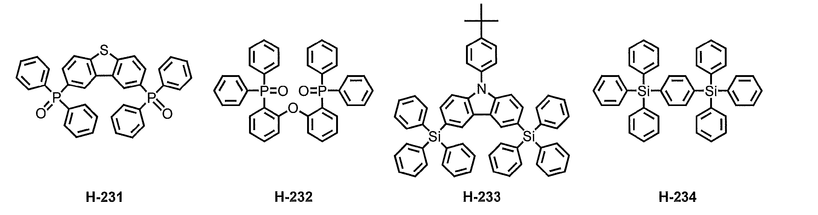
さらに、本発明に用いられるホスト化合物は、下記一般式(I)で表される化合物であることが好ましい。下記一般式(I)で表される化合物はバイポーラー性を有し、かつ非常に安定である。したがってホスト化合物が下記一般式(I)で表される化合物であると、有機EL素子の寿命が長くなりやすい。

上記一般式(I)中、X101は、NR101、酸素原子、硫黄原子、スルフィニル基、スルホニル基、CR102R103又はSiR104R105を表す。また、y1~y8は、それぞれ独立に、CR106、又は窒素原子を表す。ここで、R101~R106は、それぞれ独立に、水素原子又は置換基を表し、互いに結合して環を形成してもよい。R101~R106でありうる置換基の例には、以下の基が含まれる。
直鎖状又は分岐状のアルキル基(例えば、メチル基、エチル基、プロピル基、イソプロピル基、t-ブチル基、ペンチル基、ヘキシル基、オクチル基、ドデシル基、トリデシル基、テトラデシル基、ペンタデシル基等);
アルケニル基(例えば、ビニル基、アリル基等);
アルキニル基(例えば、エチニル基、プロパルギル基等);
芳香族炭化水素環基(芳香族炭素環基やアリール基等とも称される。例えば、ベンゼン環、ビフェニル、ナフタレン環、アズレン環、アントラセン環、フェナントレン環、ピレン環、クリセン環、ナフタセン環、トリフェニレン環、o-ターフェニル環、m-ターフェニル環、p-ターフェニル環、アセナフテン環、コロネン環、インデン環、フルオレン環、フルオラントレン環、ナフタセン環、ペンタセン環、ペリレン環、ペンタフェン環、ピセン環、ピレン環、ピラントレン環、アンスラアントレン環、テトラリン等から導出される基);
芳香族複素環基(例えば、フラン環、ジベンゾフラン環、チオフェン環、ジベンゾチオフェン環、オキサゾール環、ピロール環、ピリジン環、ピリダジン環、ピリミジン環、ピラジン環、トリアジン環、ベンゾイミダゾール環、オキサジアゾール環、トリアゾール環、イミダゾール環、ピラゾール環、チアゾール環、インドール環、インダゾール環、ベンゾイミダゾール環、ベンゾチアゾール環、ベンゾオキサゾール環、キノキサリン環、キナゾリン環、シンノリン環、キノリン環、イソキノリン環、フタラジン環、ナフチリジン環、カルバゾール環、カルボリン環、ジアザカルバゾール環(カルボリン環を構成する炭化水素環の炭素原子の一つが更に窒素原子で置換されている環等から導出される基。また、カルボリン環とジアザカルバゾール環を合わせて「アザカルバゾール環」と称される場合もある。);
非芳香族炭化水素環基(例えば、シクロペンチル基、シクロヘキシル基等);
非芳香族複素環基(例えば、ピロリジル基、イミダゾリジル基、モルホリル基、オキサゾリジル基等);
アルコキシ基(例えば、メトキシ基、エトキシ基、プロピルオキシ基、ペンチルオキシ基、ヘキシルオキシ基、オクチルオキシ基、ドデシルオキシ基等);
シクロアルコキシ基(例えば、シクロペンチルオキシ基、シクロヘキシルオキシ基等);
アリールオキシ基(例えば、フェノキシ基、ナフチルオキシ基等);
アルキルチオ基(例えば、メチルチオ基、エチルチオ基、プロピルチオ基、ペンチルチオ基、ヘキシルチオ基、オクチルチオ基、ドデシルチオ基等);
シクロアルキルチオ基(例えば、シクロペンチルチオ基、シクロヘキシルチオ基等);
アリールチオ基(例えば、フェニルチオ基、ナフチルチオ基等):
アルコキシカルボニル基(例えば、メチルオキシカルボニル基、エチルオキシカルボニル基、ブチルオキシカルボニル基、オクチルオキシカルボニル基、ドデシルオキシカルボニル基等);
アリールオキシカルボニル基(例えば、フェニルオキシカルボニル基、ナフチルオキシカルボニル基等);
スルファモイル基(例えば、アミノスルホニル基、メチルアミノスルホニル基、ジメチルアミノスルホニル基、ブチルアミノスルホニル基、ヘキシルアミノスルホニル基、シクロヘキシルアミノスルホニル基、オクチルアミノスルホニル基、ドデシルアミノスルホニル基、フェニルアミノスルホニル基、ナフチルアミノスルホニル基、2-ピリジルアミノスルホニル基等);
アシル基(例えば、アセチル基、エチルカルボニル基、プロピルカルボニル基、ペンチルカルボニル基、シクロヘキシルカルボニル基、オクチルカルボニル基、2-エチルヘキシルカルボニル基、ドデシルカルボニル基、フェニルカルボニル基、ナフチルカルボニル基、ピリジルカルボニル基等);
アシルオキシ基(例えば、アセチルオキシ基、エチルカルボニルオキシ基、ブチルカルボニルオキシ基、オクチルカルボニルオキシ基、ドデシルカルボニルオキシ基、フェニルカルボニルオキシ基等);
アミド基(例えば、メチルカルボニルアミノ基、エチルカルボニルアミノ基、ジメチルカルボニルアミノ基、プロピルカルボニルアミノ基、ペンチルカルボニルアミノ基、シクロヘキシルカルボニルアミノ基、2-エチルヘキシルカルボニルアミノ基、オクチルカルボニルアミノ基、ドデシルカルボニルアミノ基、フェニルカルボニルアミノ基、ナフチルカルボニルアミノ基等);
カルバモイル基(例えば、アミノカルボニル基、メチルアミノカルボニル基、ジメチルアミノカルボニル基、プロピルアミノカルボニル基、ペンチルアミノカルボニル基、シクロヘキシルアミノカルボニル基、オクチルアミノカルボニル基、2-エチルヘキシルアミノカルボニル基、ドデシルアミノカルボニル基、フェニルアミノカルボニル基、ナフチルアミノカルボニル基、2-ピリジルアミノカルボニル基等);
ウレイド基(例えば、メチルウレイド基、エチルウレイド基、ペンチルウレイド基、シクロヘキシルウレイド基、オクチルウレイド基、ドデシルウレイド基、フェニルウレイド基ナフチルウレイド基、2-ピリジルアミノウレイド基等);
スルフィニル基(例えば、メチルスルフィニル基、エチルスルフィニル基、ブチルスルフィニル基、シクロヘキシルスルフィニル基、2-エチルヘキシルスルフィニル基、ドデシルスルフィニル基、フェニルスルフィニル基、ナフチルスルフィニル基、2-ピリジルスルフィニル基等);
アルキルスルホニル基(例えば、メチルスルホニル基、エチルスルホニル基、ブチルスルホニル基、シクロヘキシルスルホニル基、2-エチルヘキシルスルホニル基、ドデシルスルホニル基等);
アリールスルホニル基又はヘテロアリールスルホニル基(例えば、フェニルスルホニル基、ナフチルスルホニル基、2-ピリジルスルホニル基等);
アミノ基(例えば、アミノ基、エチルアミノ基、ジメチルアミノ基、ブチルアミノ基、シクロペンチルアミノ基、2-エチルヘキシルアミノ基、ドデシルアミノ基、アニリノ基、ナフチルアミノ基、2-ピリジルアミノ基、ジフェニルアミノ基等);
ハロゲン原子(例えば、フッ素原子、塩素原子、臭素原子等);
フッ化炭化水素基(例えば、フルオロメチル基、トリフルオロメチル基、ペンタフルオロエチル基、ペンタフルオロフェニル基等);
シアノ基;
ニトロ基;
ヒドロキシ基;
チオール基;
シリル基(例えば、トリメチルシリル基、トリイソプロピルシリル基、トリフェニルシリル基、フェニルジエチルシリル基等);
重水素原子
アルケニル基(例えば、ビニル基、アリル基等);
アルキニル基(例えば、エチニル基、プロパルギル基等);
芳香族炭化水素環基(芳香族炭素環基やアリール基等とも称される。例えば、ベンゼン環、ビフェニル、ナフタレン環、アズレン環、アントラセン環、フェナントレン環、ピレン環、クリセン環、ナフタセン環、トリフェニレン環、o-ターフェニル環、m-ターフェニル環、p-ターフェニル環、アセナフテン環、コロネン環、インデン環、フルオレン環、フルオラントレン環、ナフタセン環、ペンタセン環、ペリレン環、ペンタフェン環、ピセン環、ピレン環、ピラントレン環、アンスラアントレン環、テトラリン等から導出される基);
芳香族複素環基(例えば、フラン環、ジベンゾフラン環、チオフェン環、ジベンゾチオフェン環、オキサゾール環、ピロール環、ピリジン環、ピリダジン環、ピリミジン環、ピラジン環、トリアジン環、ベンゾイミダゾール環、オキサジアゾール環、トリアゾール環、イミダゾール環、ピラゾール環、チアゾール環、インドール環、インダゾール環、ベンゾイミダゾール環、ベンゾチアゾール環、ベンゾオキサゾール環、キノキサリン環、キナゾリン環、シンノリン環、キノリン環、イソキノリン環、フタラジン環、ナフチリジン環、カルバゾール環、カルボリン環、ジアザカルバゾール環(カルボリン環を構成する炭化水素環の炭素原子の一つが更に窒素原子で置換されている環等から導出される基。また、カルボリン環とジアザカルバゾール環を合わせて「アザカルバゾール環」と称される場合もある。);
非芳香族炭化水素環基(例えば、シクロペンチル基、シクロヘキシル基等);
非芳香族複素環基(例えば、ピロリジル基、イミダゾリジル基、モルホリル基、オキサゾリジル基等);
アルコキシ基(例えば、メトキシ基、エトキシ基、プロピルオキシ基、ペンチルオキシ基、ヘキシルオキシ基、オクチルオキシ基、ドデシルオキシ基等);
シクロアルコキシ基(例えば、シクロペンチルオキシ基、シクロヘキシルオキシ基等);
アリールオキシ基(例えば、フェノキシ基、ナフチルオキシ基等);
アルキルチオ基(例えば、メチルチオ基、エチルチオ基、プロピルチオ基、ペンチルチオ基、ヘキシルチオ基、オクチルチオ基、ドデシルチオ基等);
シクロアルキルチオ基(例えば、シクロペンチルチオ基、シクロヘキシルチオ基等);
アリールチオ基(例えば、フェニルチオ基、ナフチルチオ基等):
アルコキシカルボニル基(例えば、メチルオキシカルボニル基、エチルオキシカルボニル基、ブチルオキシカルボニル基、オクチルオキシカルボニル基、ドデシルオキシカルボニル基等);
アリールオキシカルボニル基(例えば、フェニルオキシカルボニル基、ナフチルオキシカルボニル基等);
スルファモイル基(例えば、アミノスルホニル基、メチルアミノスルホニル基、ジメチルアミノスルホニル基、ブチルアミノスルホニル基、ヘキシルアミノスルホニル基、シクロヘキシルアミノスルホニル基、オクチルアミノスルホニル基、ドデシルアミノスルホニル基、フェニルアミノスルホニル基、ナフチルアミノスルホニル基、2-ピリジルアミノスルホニル基等);
アシル基(例えば、アセチル基、エチルカルボニル基、プロピルカルボニル基、ペンチルカルボニル基、シクロヘキシルカルボニル基、オクチルカルボニル基、2-エチルヘキシルカルボニル基、ドデシルカルボニル基、フェニルカルボニル基、ナフチルカルボニル基、ピリジルカルボニル基等);
アシルオキシ基(例えば、アセチルオキシ基、エチルカルボニルオキシ基、ブチルカルボニルオキシ基、オクチルカルボニルオキシ基、ドデシルカルボニルオキシ基、フェニルカルボニルオキシ基等);
アミド基(例えば、メチルカルボニルアミノ基、エチルカルボニルアミノ基、ジメチルカルボニルアミノ基、プロピルカルボニルアミノ基、ペンチルカルボニルアミノ基、シクロヘキシルカルボニルアミノ基、2-エチルヘキシルカルボニルアミノ基、オクチルカルボニルアミノ基、ドデシルカルボニルアミノ基、フェニルカルボニルアミノ基、ナフチルカルボニルアミノ基等);
カルバモイル基(例えば、アミノカルボニル基、メチルアミノカルボニル基、ジメチルアミノカルボニル基、プロピルアミノカルボニル基、ペンチルアミノカルボニル基、シクロヘキシルアミノカルボニル基、オクチルアミノカルボニル基、2-エチルヘキシルアミノカルボニル基、ドデシルアミノカルボニル基、フェニルアミノカルボニル基、ナフチルアミノカルボニル基、2-ピリジルアミノカルボニル基等);
ウレイド基(例えば、メチルウレイド基、エチルウレイド基、ペンチルウレイド基、シクロヘキシルウレイド基、オクチルウレイド基、ドデシルウレイド基、フェニルウレイド基ナフチルウレイド基、2-ピリジルアミノウレイド基等);
スルフィニル基(例えば、メチルスルフィニル基、エチルスルフィニル基、ブチルスルフィニル基、シクロヘキシルスルフィニル基、2-エチルヘキシルスルフィニル基、ドデシルスルフィニル基、フェニルスルフィニル基、ナフチルスルフィニル基、2-ピリジルスルフィニル基等);
アルキルスルホニル基(例えば、メチルスルホニル基、エチルスルホニル基、ブチルスルホニル基、シクロヘキシルスルホニル基、2-エチルヘキシルスルホニル基、ドデシルスルホニル基等);
アリールスルホニル基又はヘテロアリールスルホニル基(例えば、フェニルスルホニル基、ナフチルスルホニル基、2-ピリジルスルホニル基等);
アミノ基(例えば、アミノ基、エチルアミノ基、ジメチルアミノ基、ブチルアミノ基、シクロペンチルアミノ基、2-エチルヘキシルアミノ基、ドデシルアミノ基、アニリノ基、ナフチルアミノ基、2-ピリジルアミノ基、ジフェニルアミノ基等);
ハロゲン原子(例えば、フッ素原子、塩素原子、臭素原子等);
フッ化炭化水素基(例えば、フルオロメチル基、トリフルオロメチル基、ペンタフルオロエチル基、ペンタフルオロフェニル基等);
シアノ基;
ニトロ基;
ヒドロキシ基;
チオール基;
シリル基(例えば、トリメチルシリル基、トリイソプロピルシリル基、トリフェニルシリル基、フェニルジエチルシリル基等);
重水素原子
上記の中でも好ましい基として、直鎖又は分岐アルキル基、芳香族炭化水素環基、芳香族複素環基、アミノ基、フッ素原子、フッ化炭化水素基、シアノ基、及びシリル基が挙げられる。
また、Ar101及びAr102は、それぞれ独立に、置換されていてもよいアリール基、又は置換されていてもよいヘテロアリール基を表す。「置換されていてもよいアリール基」におけるアリール基は、炭素原子数6~24の芳香族炭化水素環から誘導される基であることが好ましい。そのような芳香族炭化水素環の例には、ベンゼン環、インデン環、ナフタレン環、アズレン環、フルオレン環、フェナントレン環、アントラセン環、アセナフチレン環、ビフェニレン環、ナフタセン環、ピレン環、ペンタレン環、アセアントリレン環、ヘプタレン環、トリフェニレン環、as-インダセン環、クリセン環、s-インダセン環、プレイアデン環、フェナレン環、フルオランテン環、ペリレン環、アセフェナントリレン環、ビフェニル環、ターフェニル環、及びテトラフェニル環等が含まれる。好ましくは、ベンゼン環、ビフェニル環、ターフェニル環である。
また、「置換されていてもよいヘテロアリール基」におけるヘテロアリール基は、各種芳香族複素環から誘導される基であることが好ましい。そのような芳香族複素環の例にはピロール環、インドール環、カルバゾール環、インドロインドール環、9,10-ジヒドロアクリジン環、5,10-ジヒドロフェナジン環、フェノキサジン環、フェノチアジン環、ジベンゾチオフェン環、ベンゾフリルインドール環、ベンゾチエノインドール環、インドロカルバゾール環、ベンゾフリルカルバゾール環、ベンゾチエノカルバゾール環、ベンゾチエノベンゾチオフェン環、ベンゾカルバゾール環、ジベンゾカルバゾール環、アザカルバゾール環、アザジベンゾフラン環、ジアザカルバゾール環、ジアザジベンゾフラン環、ジベンゾチオフェンオキシド環、ジベンゾチオフェンジオキシド環、ピリジン環、ピリダジン環、ピリミジン環、ピラジン環、トリアジン環、キノリン環、イソキノリン環、キナゾリン環、シンノリン環、キノキサリン環、フタラジン環、プテリジン環、フェナントリジン環、フェナントロリン環、ジベンゾフラン環、ジベンゾシロール環、ジベンゾボロール環、ジベンゾホスホールオキシド環等が含まれる。好ましくは、カルバゾール環、ベンゾカルバゾール環、アザカルバゾール環、アザジベンゾフラン環、ジアザカルバゾール環、ジアザジベンゾフラン環、ピリジン環、ピリミジン環、トリアジン環である。
アリール基やヘテロアリール基が有しうる置換基の例には、アルキル基で置換されていてもよいアリール基、フッ素原子、シアノ基、フッ素で置換されていてもよいアルキル基、置換されていてもよいカルボニル基、置換されていてもよいスルホニル基、置換されていてもよいホスフィンオキサイド基、置換されていてもよいボリル基、置換されていてもよい複素環基、置換されていてもよいアミノ基、置換されていてもよいシリル基等が含まれる。
上記「アルキル基」は、直鎖、分岐又は環状のいずれであってもよく、例えば炭素原子数1~20の直鎖又は分岐のアルキル基、或いは炭素原子数5~20の環状のアルキル基でありうる。アルキル基の例には、メチル基、エチル基、n-プロピル基、イソプロピル基、n-ブチル基、s-ブチル基、t-ブチル基、n-ペンチル基、ネオペンチル基、n-ヘキシル基、シクロヘキシル基、2-エチルヘキシル基、n-ヘプチル基、n-オクチル基、2-ヘキシルオクチル基、n-ノニル基、n-デシル基、n-ウンデシル基、n-ドデシル基、n-トリデシル基、n-テトラデシル基、n-ペンタデシル基、n-ヘキサデシル基、n-ヘプタデシル基、n-オクタデシル基、n-ノナデシル基、及びn-イコシル基等が含まれる。また、「アリール基」及び「複素環基」は、Ar101及びAr102で表されるアリール基やヘテロアリール基と同様でありうる。
上記「アルキル基」は、直鎖、分岐又は環状のいずれであってもよく、例えば炭素原子数1~20の直鎖又は分岐のアルキル基、或いは炭素原子数5~20の環状のアルキル基でありうる。アルキル基の例には、メチル基、エチル基、n-プロピル基、イソプロピル基、n-ブチル基、s-ブチル基、t-ブチル基、n-ペンチル基、ネオペンチル基、n-ヘキシル基、シクロヘキシル基、2-エチルヘキシル基、n-ヘプチル基、n-オクチル基、2-ヘキシルオクチル基、n-ノニル基、n-デシル基、n-ウンデシル基、n-ドデシル基、n-トリデシル基、n-テトラデシル基、n-ペンタデシル基、n-ヘキサデシル基、n-ヘプタデシル基、n-オクタデシル基、n-ノナデシル基、及びn-イコシル基等が含まれる。また、「アリール基」及び「複素環基」は、Ar101及びAr102で表されるアリール基やヘテロアリール基と同様でありうる。
また、上記一般式(I)において、n101及びn102は、各々0~4の整数を表すが、R101が水素原子の場合は、n101は1~4の整数を表す。
上記一般式(I)で表される構造を有するホスト化合物は、下記一般式(II)で表される構造を有することがより好ましい。

一般式(II)において、X101は、NR101、酸素原子、硫黄原子、スルフィニル基、スルホニル基、CR102R103又はSiR104R105を表す。R101~R105は、それぞれ独立して水素原子又は置換基を表し、互いに結合して環を形成してもよい。なお、R101~R105は、一般式(I)のR101~R105と同義である。
Ar101及びAr102は、それぞれ独立に、置換されていてもよいアリール基、置換されていてもよいヘテロアリール基を表し、Ar101及びAr102は、一般式(I)のAr101及びAr102と同義である。
また、n102は0~4の整数を表す。
さらに、一般式(II)で表される化合物は、下記一般式(III-1)、(III-2)又は(III-3)で表される化合物であることが好ましい。

一般式(III-1)~(III-3)において、X101、Ar102、n102は、前記一般式(II)におけるX101、Ar102、n102と同義である。また、一般式(III-2)において、R104は、前記一般式(I)におけるR104と同義である。
一般式(III-1)~(III-3)において、X101を含んで形成される縮合環、カルバゾール環及びベンゼン環は、ホスト化合物の機能を阻害しない範囲でさらに置換基を有してもよい。
一般式(III-1)~(III-3)において、X101を含んで形成される縮合環、カルバゾール環及びベンゼン環は、ホスト化合物の機能を阻害しない範囲でさらに置換基を有してもよい。
上記一般式(I)、(II)、又は(III-1)~(III-3)で表されるホスト化合物の好ましい具体例を挙げるが、これらの化合物はさらに置換基を有していたり、構造異性体などが存在していたりする場合もあり、本記述に限定されない。

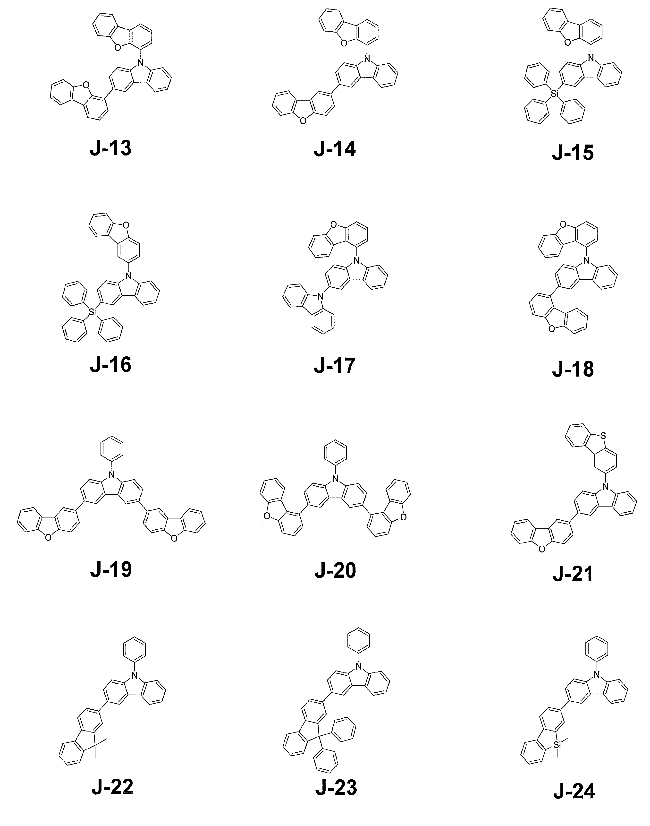
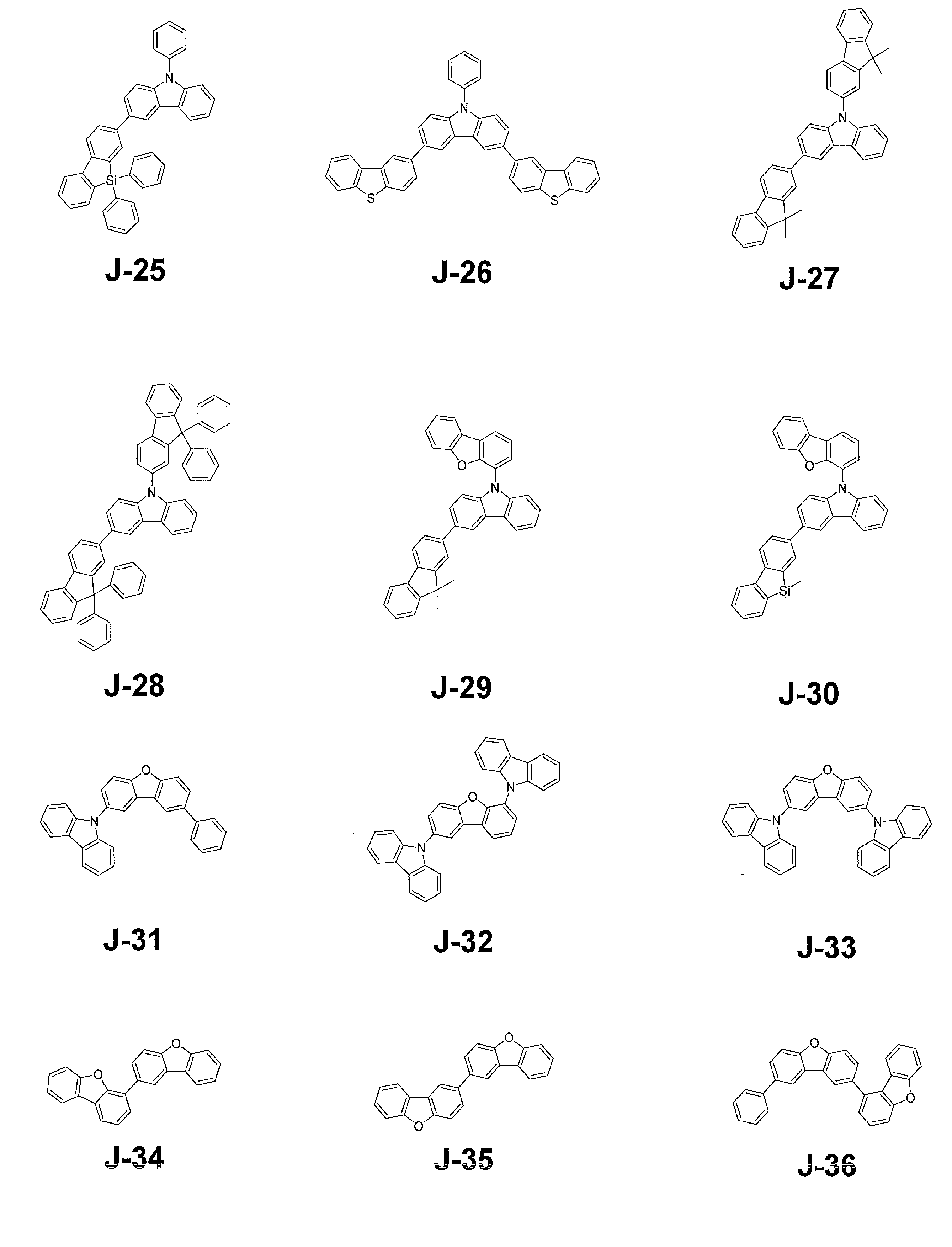
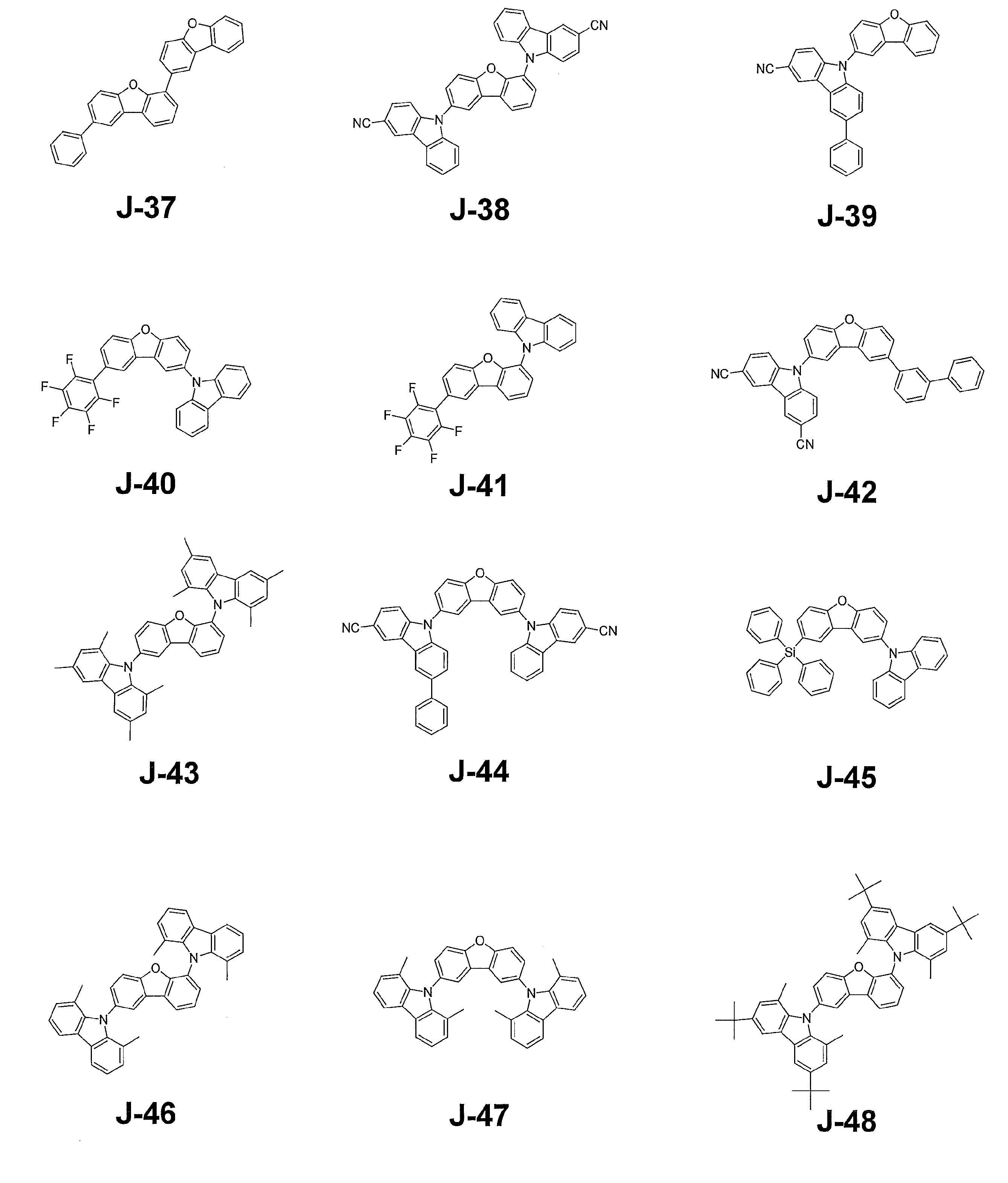
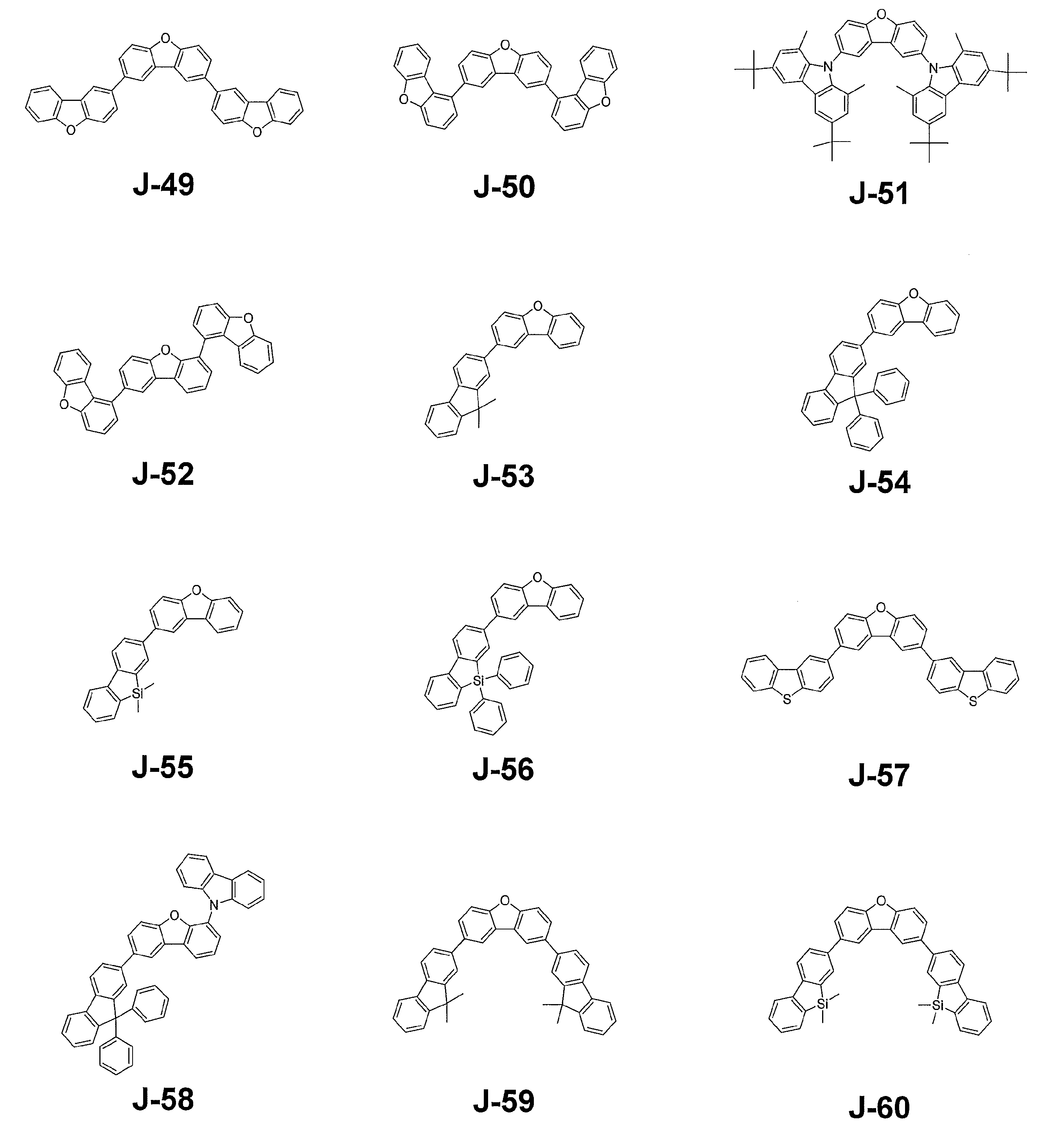

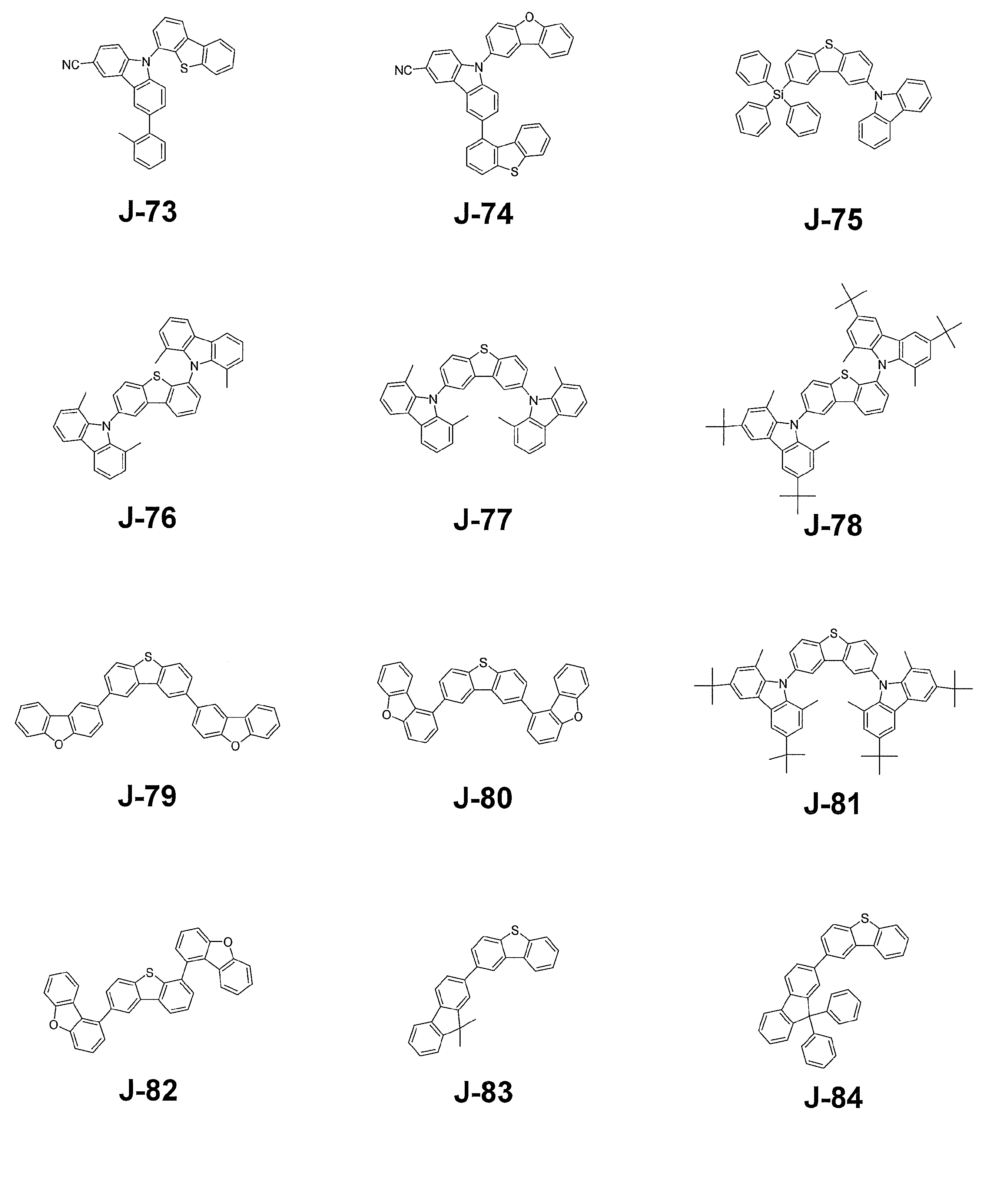
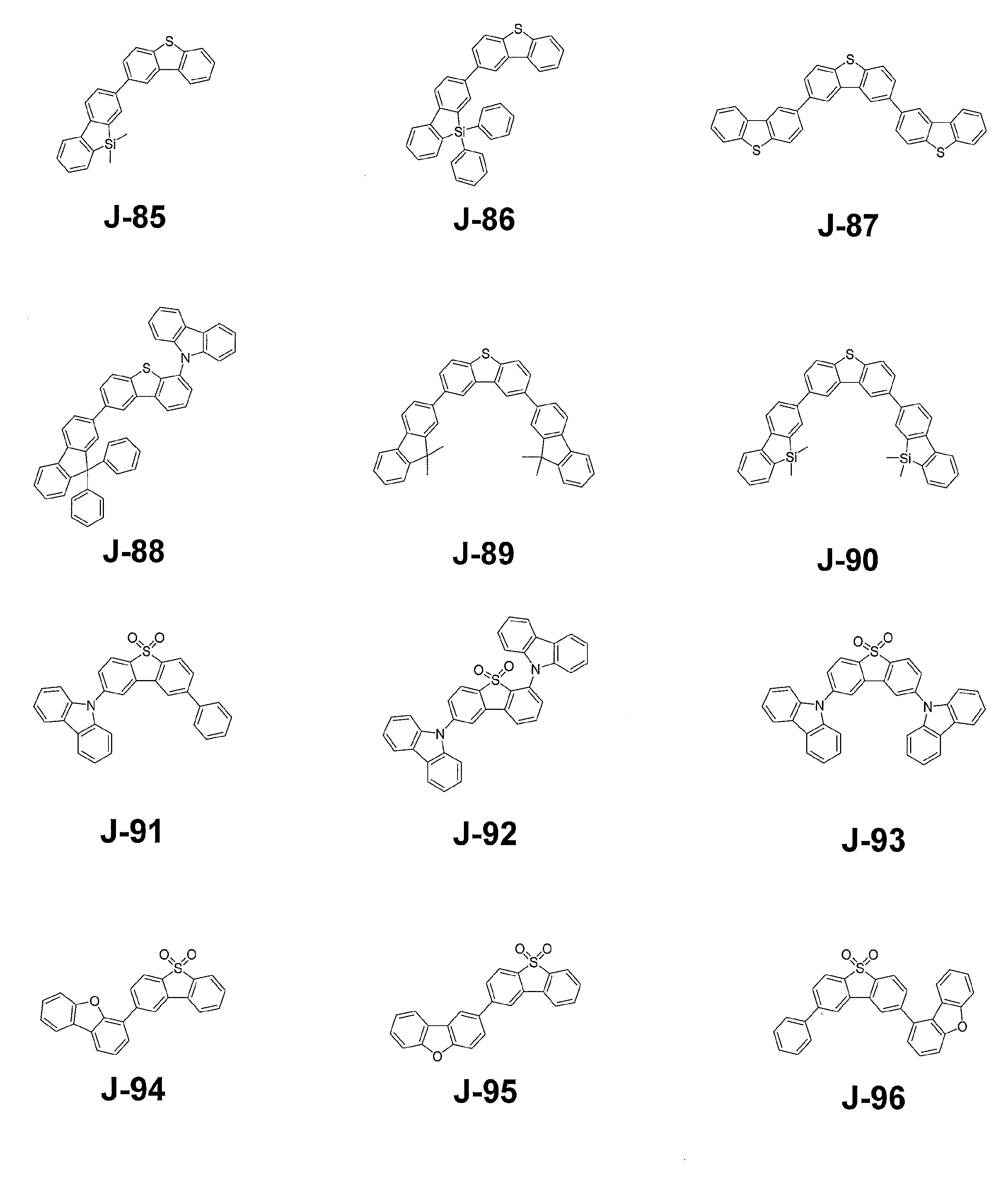
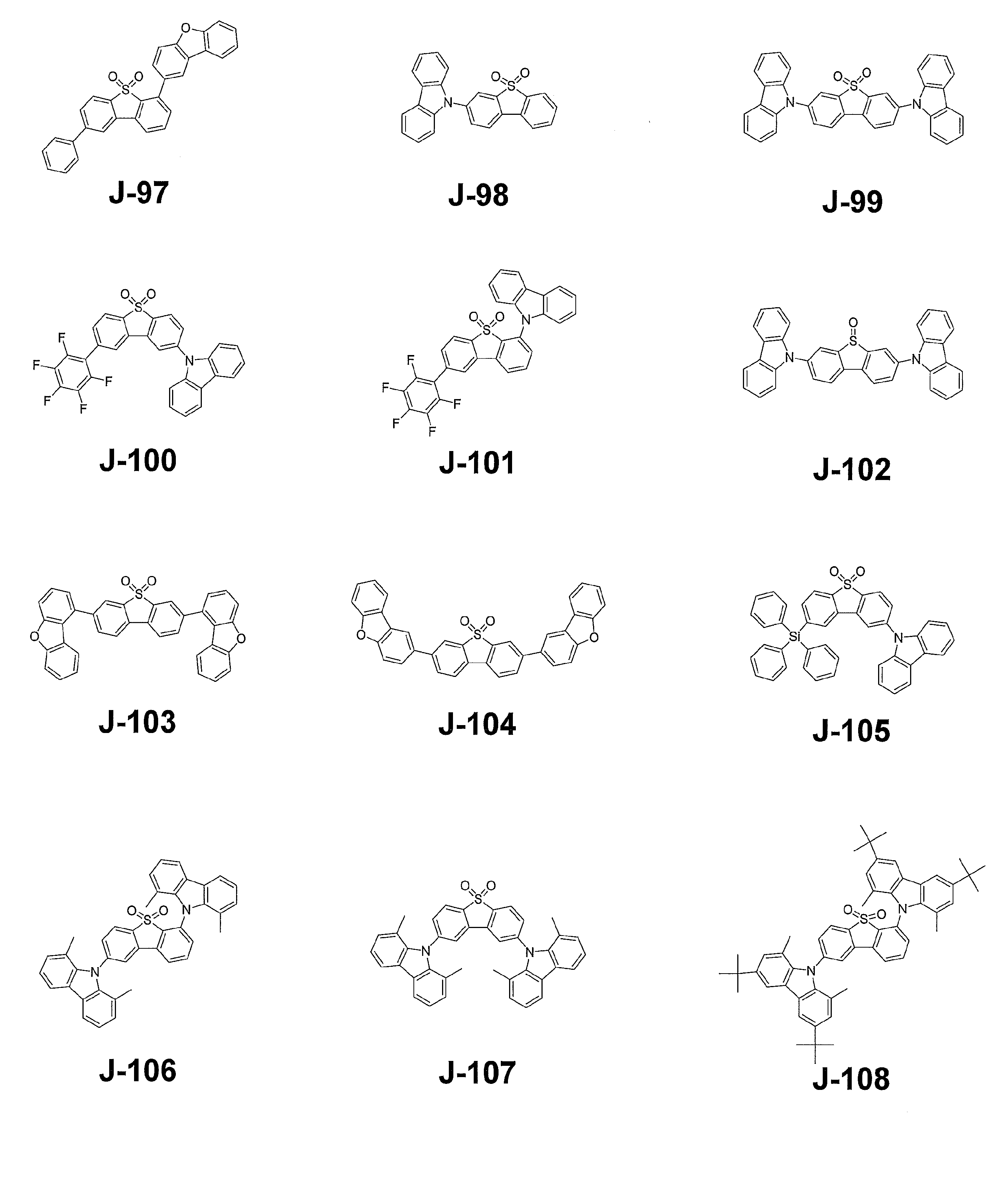

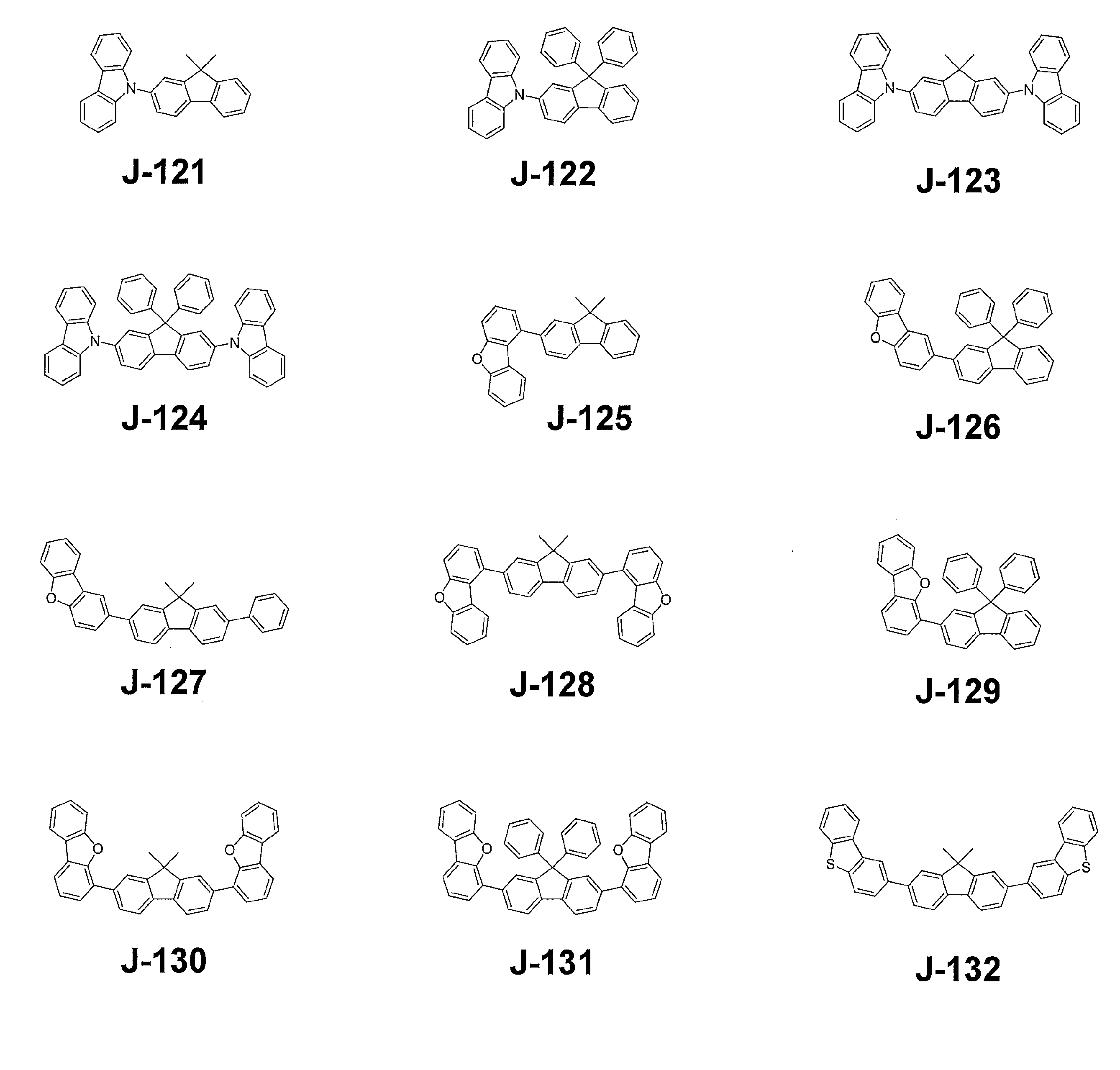


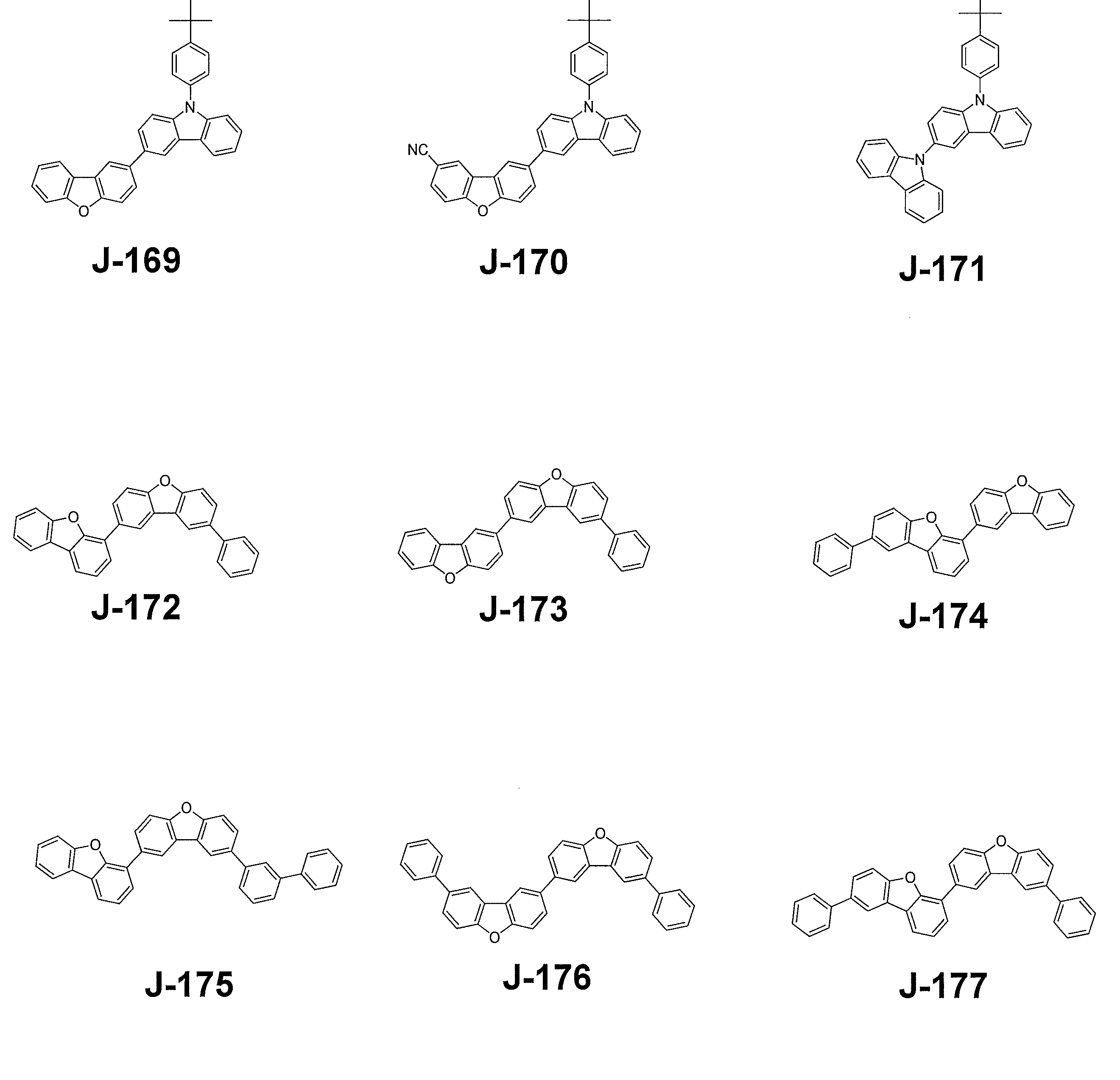
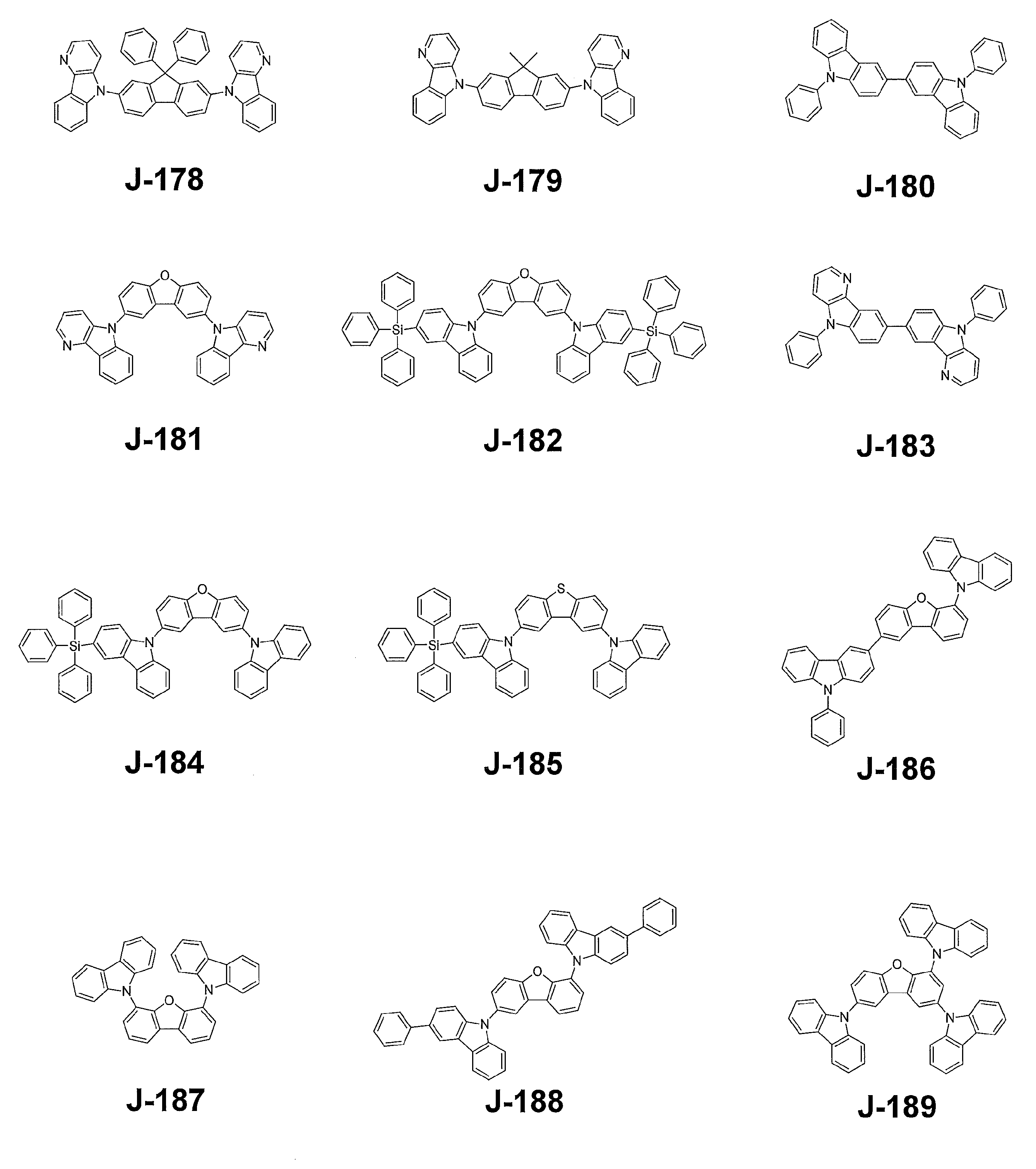


《電子輸送層》
本発明において電子輸送層とは、電子を輸送する機能を有する材料からなり、陰極より注入された電子を発光層に伝達する機能を有していればよい。
本発明に係る電子輸送層の総層厚については特に制限はないが、通常は2nm~5μmの範囲であり、より好ましくは2~500nmであり、さらに好ましくは5~200nmである。
また、有機EL素子においては発光層で生じた光を電極から取り出す際、発光層から直接取り出される光と、光を取り出す電極と対極に位置する電極によって反射されてから取り出される光とが干渉を起こすことが知られている。光が陰極で反射される場合は、電子輸送層の総層厚を数nm~数μmの間で適宜調整することにより、この干渉効果を効率的に利用することが可能である。
一方で、電子輸送層の層厚を厚くすると電圧が上昇しやすくなるため、特に層厚が厚い場合においては、電子輸送層の電子移動度は10-5cm2/Vs以上であることが好ましい。
電子輸送層に用いられる材料(以下、電子輸送材料という)としては、電子の注入性又は輸送性、正孔の障壁性のいずれかを有していればよく、従来公知の化合物の中から任意のものを選択して用いることができる。
本発明において電子輸送層とは、電子を輸送する機能を有する材料からなり、陰極より注入された電子を発光層に伝達する機能を有していればよい。
本発明に係る電子輸送層の総層厚については特に制限はないが、通常は2nm~5μmの範囲であり、より好ましくは2~500nmであり、さらに好ましくは5~200nmである。
また、有機EL素子においては発光層で生じた光を電極から取り出す際、発光層から直接取り出される光と、光を取り出す電極と対極に位置する電極によって反射されてから取り出される光とが干渉を起こすことが知られている。光が陰極で反射される場合は、電子輸送層の総層厚を数nm~数μmの間で適宜調整することにより、この干渉効果を効率的に利用することが可能である。
一方で、電子輸送層の層厚を厚くすると電圧が上昇しやすくなるため、特に層厚が厚い場合においては、電子輸送層の電子移動度は10-5cm2/Vs以上であることが好ましい。
電子輸送層に用いられる材料(以下、電子輸送材料という)としては、電子の注入性又は輸送性、正孔の障壁性のいずれかを有していればよく、従来公知の化合物の中から任意のものを選択して用いることができる。
例えば、含窒素芳香族複素環誘導体(カルバゾール誘導体、アザカルバゾール誘導体(カルバゾール環を構成する炭素原子の一つ以上が窒素原子に置換されたもの)、ピリジン誘導体、ピリミジン誘導体、ピラジン誘導体、ピリダジン誘導体、トリアジン誘導体、キノリン誘導体、キノキサリン誘導体、フェナントロリン誘導体、アザトリフェニレン誘導体、オキサゾール誘導体、チアゾール誘導体、オキサジアゾール誘導体、チアジアゾール誘導体、トリアゾール誘導体、ベンズイミダゾール誘導体、ベンズオキサゾール誘導体、ベンズチアゾール誘導体等)、ジベンゾフラン誘導体、ジベンゾチオフェン誘導体、シロール誘導体、芳香族炭化水素環誘導体(ナフタレン誘導体、アントラセン誘導体、トリフェニレン誘導体等)等が挙げられる。
また、配位子にキノリノール骨格やジベンゾキノリノール骨格を有する金属錯体、例えば、トリス(8-キノリノール)アルミニウム(Alq)、トリス(5,7-ジクロロ-8-キノリノール)アルミニウム、トリス(5,7-ジブロモ-8-キノリノール)アルミニウム、トリス(2-メチル-8-キノリノール)アルミニウム、トリス(5-メチル-8-キノリノール)アルミニウム、ビス(8-キノリノール)亜鉛(Znq)等、及びこれらの金属錯体の中心金属がIn、Mg、Cu、Ca、Sn、Ga又はPbに置き替わった金属錯体も、電子輸送材料として用いることができる。
その他、メタルフリー若しくはメタルフタロシアニン、又はそれらの末端がアルキル基やスルホン酸基等で置換されているものも、電子輸送材料として好ましく用いることができる。また、発光層の材料として例示したジスチリルピラジン誘導体も、電子輸送材料として用いることができるし、正孔注入層、正孔輸送層と同様にn型-Si、n型-SiC等の無機半導体も電子輸送材料として用いることができる。
また、これらの材料を高分子鎖に導入した、又はこれらの材料を高分子の主鎖とした高分子材料を用いることもできる。
その他、メタルフリー若しくはメタルフタロシアニン、又はそれらの末端がアルキル基やスルホン酸基等で置換されているものも、電子輸送材料として好ましく用いることができる。また、発光層の材料として例示したジスチリルピラジン誘導体も、電子輸送材料として用いることができるし、正孔注入層、正孔輸送層と同様にn型-Si、n型-SiC等の無機半導体も電子輸送材料として用いることができる。
また、これらの材料を高分子鎖に導入した、又はこれらの材料を高分子の主鎖とした高分子材料を用いることもできる。
本発明に係る電子輸送層においては、電子輸送層にドープ材をゲスト材料としてドープして、n性の高い(電子リッチ)電子輸送層を形成してもよい。ドープ材としては、金属錯体やハロゲン化金属など金属化合物等のn型ドーパントが挙げられる。このような構成の電子輸送層の具体例としては、例えば、特開平4-297076号公報、同10-270172号公報、特開2000-196140号公報、同2001-102175号公報、J.Appl.Phys.,95,5773(2004)等の文献に記載されたものが挙げられる。
本発明の有機EL素子に用いられる、公知の好ましい電子輸送材料の具体例としては、以下の文献に記載の化合物等が挙げられるが、本発明はこれらに限定されない。
米国特許第6528187号明細書、米国特許第7230107号明細書、米国特許出願公開第2005/0025993号明細書、米国特許出願公開第2004/0036077号明細書、米国特許出願公開第2009/0115316号明細書、米国特許出願公開第2009/0101870号明細書、米国特許出願公開第2009/0179554号明細書、国際公開第2003/060956号、国際公開第2008/132085号、Appl.Phys.Lett.75,4(1999)、Appl.Phys.Lett.79,449(2001)、Appl.Phys.Lett.81,162(2002)、Appl.Phys.Lett.81,162(2002)、Appl.Phys.Lett.79,156(2001)、米国特許第7964293号明細書、米国特許出願公開第2009/030202号明細書、国際公開第2004/080975号、国際公開第2004/063159号、国際公開第2005/085387号、国際公開第2006/067931号、国際公開第2007/086552号、国際公開第2008/114690号、国際公開第2009/069442号、国際公開第2009/066779号、国際公開第2009/054253号、国際公開第2011/086935号、国際公開第2010/150593号、国際公開第2010/047707号、欧州特許第2311826号明細書、特開2010-251675号公報、特開2009-209133号公報、特開2009-124114号公報、特開2008-277810号公報、特開2006-156445号公報、特開2005-340122号公報、特開2003-45662号公報、特開2003-31367号公報、特開2003-282270号公報、国際公開第2012/115034号等である。
米国特許第6528187号明細書、米国特許第7230107号明細書、米国特許出願公開第2005/0025993号明細書、米国特許出願公開第2004/0036077号明細書、米国特許出願公開第2009/0115316号明細書、米国特許出願公開第2009/0101870号明細書、米国特許出願公開第2009/0179554号明細書、国際公開第2003/060956号、国際公開第2008/132085号、Appl.Phys.Lett.75,4(1999)、Appl.Phys.Lett.79,449(2001)、Appl.Phys.Lett.81,162(2002)、Appl.Phys.Lett.81,162(2002)、Appl.Phys.Lett.79,156(2001)、米国特許第7964293号明細書、米国特許出願公開第2009/030202号明細書、国際公開第2004/080975号、国際公開第2004/063159号、国際公開第2005/085387号、国際公開第2006/067931号、国際公開第2007/086552号、国際公開第2008/114690号、国際公開第2009/069442号、国際公開第2009/066779号、国際公開第2009/054253号、国際公開第2011/086935号、国際公開第2010/150593号、国際公開第2010/047707号、欧州特許第2311826号明細書、特開2010-251675号公報、特開2009-209133号公報、特開2009-124114号公報、特開2008-277810号公報、特開2006-156445号公報、特開2005-340122号公報、特開2003-45662号公報、特開2003-31367号公報、特開2003-282270号公報、国際公開第2012/115034号等である。
本発明におけるより好ましい公知の電子輸送材料としては、少なくとも一つの窒素原子を含む芳香族複素環化合物や、リン原子を含む化合物が挙げられ、例えばピリジン誘導体、ピリミジン誘導体、ピラジン誘導体、トリアジン誘導体、ジベンゾフラン誘導体、ジベンゾチオフェン誘導体、アザジベンゾフラン誘導体、アザジベンゾチオフェン誘導体、カルバゾール誘導体、アザカルバゾール誘導体、ベンズイミダゾール誘導体、アリールホスフィンオキサイド誘導体などが挙げられる。
電子輸送材料は単独で用いてもよく、また複数種を併用して用いてもよい。
電子輸送材料は単独で用いてもよく、また複数種を併用して用いてもよい。
《正孔阻止層》
正孔阻止層とは広い意味では電子輸送層の機能を有する層であり、好ましくは電子を輸送する機能を有しつつ正孔を輸送する能力が小さい材料からなり、電子を輸送しつつ正孔を阻止することで電子と正孔の再結合確率を向上させることができる。
また、前述する電子輸送層の構成を必要に応じて、本発明に係る正孔阻止層として用いることができる。
本発明の有機EL素子に設ける正孔阻止層は、発光層の陰極側に隣接して設けられることが好ましい。
本発明に係る正孔阻止層の層厚としては、好ましくは3~100nmの範囲であり、更に好ましくは5~30nmの範囲である。
正孔阻止層に用いられる材料としては、前述の電子輸送層に用いられる材料が好ましく用いられ、また、前述のホスト化合物として用いられる材料も正孔阻止層に好ましく用いられる。
正孔阻止層とは広い意味では電子輸送層の機能を有する層であり、好ましくは電子を輸送する機能を有しつつ正孔を輸送する能力が小さい材料からなり、電子を輸送しつつ正孔を阻止することで電子と正孔の再結合確率を向上させることができる。
また、前述する電子輸送層の構成を必要に応じて、本発明に係る正孔阻止層として用いることができる。
本発明の有機EL素子に設ける正孔阻止層は、発光層の陰極側に隣接して設けられることが好ましい。
本発明に係る正孔阻止層の層厚としては、好ましくは3~100nmの範囲であり、更に好ましくは5~30nmの範囲である。
正孔阻止層に用いられる材料としては、前述の電子輸送層に用いられる材料が好ましく用いられ、また、前述のホスト化合物として用いられる材料も正孔阻止層に好ましく用いられる。
《電子注入層》
本発明に係る電子注入層(「陰極バッファー層」ともいう)とは、駆動電圧低下や発光輝度向上のために陰極と発光層との間に設けられる層のことで、「有機EL素子とその工業化最前線(1998年11月30日エヌ・ティー・エス社発行)」の第2編第2章「電極材料」(123~166頁)に詳細に記載されている。
本発明において電子注入層は必要に応じて設け、上記のごとく陰極と発光層との間、又は陰極と電子輸送層との間に存在させてもよい。
電子注入層はごく薄い膜であることが好ましく、素材にもよるがその層厚は0.1~5nmの範囲が好ましい。また構成材料が断続的に存在する不均一な層(膜)であってもよい。
本発明に係る電子注入層(「陰極バッファー層」ともいう)とは、駆動電圧低下や発光輝度向上のために陰極と発光層との間に設けられる層のことで、「有機EL素子とその工業化最前線(1998年11月30日エヌ・ティー・エス社発行)」の第2編第2章「電極材料」(123~166頁)に詳細に記載されている。
本発明において電子注入層は必要に応じて設け、上記のごとく陰極と発光層との間、又は陰極と電子輸送層との間に存在させてもよい。
電子注入層はごく薄い膜であることが好ましく、素材にもよるがその層厚は0.1~5nmの範囲が好ましい。また構成材料が断続的に存在する不均一な層(膜)であってもよい。
電子注入層は、特開平6-325871号公報、同9-17574号公報、同10-74586号公報等にもその詳細が記載されており、電子注入層に好ましく用いられる材料の具体例としては、ストロンチウムやアルミニウム等に代表される金属、フッ化リチウム、フッ化ナトリウム、フッ化カリウム等に代表されるアルカリ金属化合物、フッ化マグネシウム、フッ化カルシウム等に代表されるアルカリ土類金属化合物、酸化アルミニウムに代表される金属酸化物、8-ヒドロキシキノリネートリチウム(Liq)等に代表される金属錯体等が挙げられる。また、前述の電子輸送材料を用いることも可能である。
また、上記の電子注入層に用いられる材料は単独で用いてもよく、複数種を併用して用いてもよい。
また、上記の電子注入層に用いられる材料は単独で用いてもよく、複数種を併用して用いてもよい。
《正孔輸送層》
本発明において正孔輸送層とは、正孔を輸送する機能を有する材料からなり、陽極より注入された正孔を発光層に伝達する機能を有していればよい。
本発明に係る正孔輸送層の総層厚については特に制限はないが、通常は5nm~5μmの範囲であり、より好ましくは2~500nmであり、さらに好ましくは5~200nmである。
正孔輸送層に用いられる材料(以下、正孔輸送材料という)としては、正孔の注入性又は輸送性、電子の障壁性のいずれかを有していればよく、従来公知の化合物の中から任意のものを選択して用いることができる。
例えば、ポルフィリン誘導体、フタロシアニン誘導体、オキサゾール誘導体、オキサジアゾール誘導体、トリアゾール誘導体、イミダゾール誘導体、ピラゾリン誘導体、ピラゾロン誘導体、フェニレンジアミン誘導体、ヒドラゾン誘導体、スチルベン誘導体、ポリアリールアルカン誘導体、トリアリールアミン誘導体、カルバゾール誘導体、インドロカルバゾール誘導体、イソインドール誘導体、アントラセンやナフタレン等のアセン系誘導体、フルオレン誘導体、フルオレノン誘導体、及びポリビニルカルバゾール、芳香族アミンを主鎖又は側鎖に導入した高分子材料又はオリゴマー、ポリシラン、導電性ポリマー又はオリゴマー(例えばPEDOT/PSS、アニリン系共重合体、ポリアニリン、ポリチオフェン等)等が挙げられる。
本発明において正孔輸送層とは、正孔を輸送する機能を有する材料からなり、陽極より注入された正孔を発光層に伝達する機能を有していればよい。
本発明に係る正孔輸送層の総層厚については特に制限はないが、通常は5nm~5μmの範囲であり、より好ましくは2~500nmであり、さらに好ましくは5~200nmである。
正孔輸送層に用いられる材料(以下、正孔輸送材料という)としては、正孔の注入性又は輸送性、電子の障壁性のいずれかを有していればよく、従来公知の化合物の中から任意のものを選択して用いることができる。
例えば、ポルフィリン誘導体、フタロシアニン誘導体、オキサゾール誘導体、オキサジアゾール誘導体、トリアゾール誘導体、イミダゾール誘導体、ピラゾリン誘導体、ピラゾロン誘導体、フェニレンジアミン誘導体、ヒドラゾン誘導体、スチルベン誘導体、ポリアリールアルカン誘導体、トリアリールアミン誘導体、カルバゾール誘導体、インドロカルバゾール誘導体、イソインドール誘導体、アントラセンやナフタレン等のアセン系誘導体、フルオレン誘導体、フルオレノン誘導体、及びポリビニルカルバゾール、芳香族アミンを主鎖又は側鎖に導入した高分子材料又はオリゴマー、ポリシラン、導電性ポリマー又はオリゴマー(例えばPEDOT/PSS、アニリン系共重合体、ポリアニリン、ポリチオフェン等)等が挙げられる。
トリアリールアミン誘導体としては、α-NPD(4,4’-ビス〔N-(1-ナフチル)-N-フェニルアミノ〕ビフェニル)に代表されるベンジジン型や、MTDATAに代表されるスターバースト型、トリアリールアミン連結コア部にフルオレンやアントラセンを有する化合物等が挙げられる。
また、特表2003-519432号公報や特開2006-135145号公報等に記載されているようなヘキサアザトリフェニレン誘導体も同様に正孔輸送材料として用いることができる。
さらに不純物をドープしたp性の高い正孔輸送層を用いることもできる。その例としては、特開平4-297076号公報、特開2000-196140号公報、同2001-102175号公報の各公報、J.Appl.Phys.,95,5773(2004)等に記載されたものが挙げられる。
また、特表2003-519432号公報や特開2006-135145号公報等に記載されているようなヘキサアザトリフェニレン誘導体も同様に正孔輸送材料として用いることができる。
さらに不純物をドープしたp性の高い正孔輸送層を用いることもできる。その例としては、特開平4-297076号公報、特開2000-196140号公報、同2001-102175号公報の各公報、J.Appl.Phys.,95,5773(2004)等に記載されたものが挙げられる。
また、特開平11-251067号公報、J.Huang et.al.著文献(Applied Physics Letters 80(2002),p.139)に記載されているような、いわゆるp型正孔輸送材料やp型-Si、p型-SiC等の無機化合物を用いることもできる。さらにIr(ppy)3に代表されるような中心金属にIrやPtを有するオルトメタル化有機金属錯体も好ましく用いられる。
正孔輸送材料としては、上記のものを使用することができるが、トリアリールアミン誘導体、カルバゾール誘導体、インドロカルバゾール誘導体、アザトリフェニレン誘導体、有機金属錯体、芳香族アミンを主鎖又は側鎖に導入した高分子材料又はオリゴマー等が好ましく用いられる。
正孔輸送材料としては、上記のものを使用することができるが、トリアリールアミン誘導体、カルバゾール誘導体、インドロカルバゾール誘導体、アザトリフェニレン誘導体、有機金属錯体、芳香族アミンを主鎖又は側鎖に導入した高分子材料又はオリゴマー等が好ましく用いられる。
本発明の有機EL素子に用いられる、公知の好ましい正孔輸送材料の具体例としては、上記で挙げた文献の他、以下の文献に記載の化合物等が挙げられるが、本発明はこれらに限定されない。
例えば、Appl.Phys.Lett.69,2160(1996)、J.Lumin.72-74,985(1997)、Appl.Phys.Lett.78,673(2001)、Appl.Phys.Lett.90,183503(2007)、Appl.Phys.Lett.90,183503(2007)、Appl.Phys.Lett.51,913(1987)、Synth.Met.87,171(1997)、Synth.Met.91,209(1997)、Synth.Met.111,421(2000)、SID Symposium Digest,37,923(2006)、J.Mater.Chem.3,319(1993)、Adv.Mater.6,677(1994)、Chem.Mater.15,3148(2003)、米国特許出願公開第2003/0162053号明細書、米国特許出願公開第2002/0158242号明細書、米国特許出願公開第2006/0240279号明細書、米国特許出願公開第2008/0220265号明細書、米国特許第5061569号、国際公開第2007/002683号、国際公開第2009/018009号、EP650955、米国特許出願公開第2008/0124572号明細書、米国特許出願公開第2007/0278938号明細書、米国特許出願公開第2008/0106190号明細書、米国特許出願公開第2008/0018221号明細書、国際公開第2012/115034号、特表2003-519432号公報、特開2006-135145号公報、米国特許出願番号13/585981号等である。
正孔輸送材料は単独で用いてもよく、また複数種を併用して用いてもよい。
例えば、Appl.Phys.Lett.69,2160(1996)、J.Lumin.72-74,985(1997)、Appl.Phys.Lett.78,673(2001)、Appl.Phys.Lett.90,183503(2007)、Appl.Phys.Lett.90,183503(2007)、Appl.Phys.Lett.51,913(1987)、Synth.Met.87,171(1997)、Synth.Met.91,209(1997)、Synth.Met.111,421(2000)、SID Symposium Digest,37,923(2006)、J.Mater.Chem.3,319(1993)、Adv.Mater.6,677(1994)、Chem.Mater.15,3148(2003)、米国特許出願公開第2003/0162053号明細書、米国特許出願公開第2002/0158242号明細書、米国特許出願公開第2006/0240279号明細書、米国特許出願公開第2008/0220265号明細書、米国特許第5061569号、国際公開第2007/002683号、国際公開第2009/018009号、EP650955、米国特許出願公開第2008/0124572号明細書、米国特許出願公開第2007/0278938号明細書、米国特許出願公開第2008/0106190号明細書、米国特許出願公開第2008/0018221号明細書、国際公開第2012/115034号、特表2003-519432号公報、特開2006-135145号公報、米国特許出願番号13/585981号等である。
正孔輸送材料は単独で用いてもよく、また複数種を併用して用いてもよい。
《電子阻止層》
電子阻止層とは、広い意味では正孔輸送層の機能を有する層であり、好ましくは正孔を輸送する機能を有しつつ電子を輸送する能力が小さい材料からなり、正孔を輸送しつつ電子を阻止することで電子と正孔の再結合確率を向上させることができる。
また、前述する正孔輸送層の構成を必要に応じて、本発明に係る電子阻止層として用いることができる。
本発明の有機EL素子に設ける電子阻止層は、発光層の陽極側に隣接して設けられることが好ましい。
本発明に係る電子阻止層の層厚としては、好ましくは3~100nmの範囲内であり、更に好ましくは5~30nmの範囲内である。
電子阻止層に用いられる材料としては、前述の正孔輸送層に用いられる材料が好ましく用いられ、また、前述のホスト化合物も電子阻止層に好ましく用いられる。
電子阻止層とは、広い意味では正孔輸送層の機能を有する層であり、好ましくは正孔を輸送する機能を有しつつ電子を輸送する能力が小さい材料からなり、正孔を輸送しつつ電子を阻止することで電子と正孔の再結合確率を向上させることができる。
また、前述する正孔輸送層の構成を必要に応じて、本発明に係る電子阻止層として用いることができる。
本発明の有機EL素子に設ける電子阻止層は、発光層の陽極側に隣接して設けられることが好ましい。
本発明に係る電子阻止層の層厚としては、好ましくは3~100nmの範囲内であり、更に好ましくは5~30nmの範囲内である。
電子阻止層に用いられる材料としては、前述の正孔輸送層に用いられる材料が好ましく用いられ、また、前述のホスト化合物も電子阻止層に好ましく用いられる。
《正孔注入層》
本発明に係る正孔注入層(「陽極バッファー層」ともいう)とは、駆動電圧低下や発光輝度向上のために陽極と発光層との間に設けられる層のことで、「有機EL素子とその工業化最前線(1998年11月30日エヌ・ティー・エス社発行)」の第2編第2章「電極材料」(123~166頁)に詳細に記載されている。
本発明において正孔注入層は必要に応じて設け、上記のごとく陽極と発光層又は陽極と正孔輸送層との間に存在させてもよい。
正孔注入層は、特開平9-45479号公報、同9-260062号公報、同8-288069号公報等にもその詳細が記載されており、正孔注入層に用いられる材料としては、例えば前述の正孔輸送層に用いられる材料等が挙げられる。
中でも銅フタロシアニンに代表されるフタロシアニン誘導体、特表2003-519432号公報や特開2006-135145号公報等に記載されているようなヘキサアザトリフェニレン誘導体、酸化バナジウムに代表される金属酸化物、アモルファスカーボン、ポリアニリン(エメラルディン)やポリチオフェン等の導電性高分子、トリス(2-フェニルピリジン)イリジウム錯体等に代表されるオルトメタル化錯体、トリアリールアミン誘導体等が好ましい。
前述の正孔注入層に用いられる材料は単独で用いてもよく、また複数種を併用して用いてもよい。
本発明に係る正孔注入層(「陽極バッファー層」ともいう)とは、駆動電圧低下や発光輝度向上のために陽極と発光層との間に設けられる層のことで、「有機EL素子とその工業化最前線(1998年11月30日エヌ・ティー・エス社発行)」の第2編第2章「電極材料」(123~166頁)に詳細に記載されている。
本発明において正孔注入層は必要に応じて設け、上記のごとく陽極と発光層又は陽極と正孔輸送層との間に存在させてもよい。
正孔注入層は、特開平9-45479号公報、同9-260062号公報、同8-288069号公報等にもその詳細が記載されており、正孔注入層に用いられる材料としては、例えば前述の正孔輸送層に用いられる材料等が挙げられる。
中でも銅フタロシアニンに代表されるフタロシアニン誘導体、特表2003-519432号公報や特開2006-135145号公報等に記載されているようなヘキサアザトリフェニレン誘導体、酸化バナジウムに代表される金属酸化物、アモルファスカーボン、ポリアニリン(エメラルディン)やポリチオフェン等の導電性高分子、トリス(2-フェニルピリジン)イリジウム錯体等に代表されるオルトメタル化錯体、トリアリールアミン誘導体等が好ましい。
前述の正孔注入層に用いられる材料は単独で用いてもよく、また複数種を併用して用いてもよい。
《添加物》
前述した本発明における有機層は、更に他の添加物が含まれていてもよい。
添加物としては、例えば臭素、ヨウ素及び塩素等のハロゲン元素やハロゲン化化合物、Pd、Ca、Na等のアルカリ金属やアルカリ土類金属、遷移金属の化合物や錯体、塩等が挙げられる。
添加物の含有量は、任意に決定することができるが、含有される層の全質量%に対して1000ppm以下であることが好ましく、より好ましくは500ppm以下であり、さらに好ましくは50ppm以下である。
ただし、電子や正孔の輸送性を向上させる目的や、励起子のエネルギー移動を有利にするための目的などによってはこの範囲内ではない。
前述した本発明における有機層は、更に他の添加物が含まれていてもよい。
添加物としては、例えば臭素、ヨウ素及び塩素等のハロゲン元素やハロゲン化化合物、Pd、Ca、Na等のアルカリ金属やアルカリ土類金属、遷移金属の化合物や錯体、塩等が挙げられる。
添加物の含有量は、任意に決定することができるが、含有される層の全質量%に対して1000ppm以下であることが好ましく、より好ましくは500ppm以下であり、さらに好ましくは50ppm以下である。
ただし、電子や正孔の輸送性を向上させる目的や、励起子のエネルギー移動を有利にするための目的などによってはこの範囲内ではない。
《有機層の形成方法》
本発明に係る有機層(正孔注入層、正孔輸送層、発光層、正孔阻止層、電子輸送層、電子注入層、中間層等)の形成方法について説明する。
本発明に係る有機層の形成方法は、特に制限はなく、従来公知の例えば真空蒸着法、湿式法(ウェットプロセスともいう)等による形成方法を用いることができる。
湿式法としては、スピンコート法、キャスト法、インクジェット法、印刷法、ダイコート法、ブレードコート法、ロールコート法、スプレーコート法、カーテンコート法、LB法(ラングミュア-ブロジェット法)等があるが、均質な薄膜が得られやすく、かつ高生産性の点から、ダイコート法、ロールコート法、インクジェット法、スプレーコート法などのロール・ツー・ロール方式適性の高い方法が好ましい。
本発明に係る有機層(正孔注入層、正孔輸送層、発光層、正孔阻止層、電子輸送層、電子注入層、中間層等)の形成方法について説明する。
本発明に係る有機層の形成方法は、特に制限はなく、従来公知の例えば真空蒸着法、湿式法(ウェットプロセスともいう)等による形成方法を用いることができる。
湿式法としては、スピンコート法、キャスト法、インクジェット法、印刷法、ダイコート法、ブレードコート法、ロールコート法、スプレーコート法、カーテンコート法、LB法(ラングミュア-ブロジェット法)等があるが、均質な薄膜が得られやすく、かつ高生産性の点から、ダイコート法、ロールコート法、インクジェット法、スプレーコート法などのロール・ツー・ロール方式適性の高い方法が好ましい。
本発明に用いられる有機EL材料を溶解又は分散する液媒体としては、例えば、メチルエチルケトン、シクロヘキサノン等のケトン類、酢酸エチル等の脂肪酸エステル類、ジクロロベンゼン等のハロゲン化炭化水素類、トルエン、キシレン、メシチレン、シクロヘキシルベンゼン等の芳香族炭化水素類、シクロヘキサン、デカリン、ドデカン等の脂肪族炭化水素類、DMF、DMSO等の有機溶媒を用いることができる。
また、分散方法としては、超音波、高剪断力分散やメディア分散等の分散方法により分散することができる。
更に層ごとに異なる成膜法を適用してもよい。成膜に蒸着法を採用する場合、その蒸着条件は使用する化合物の種類等により異なるが、一般にボート加熱温度50~450℃、真空度10-6~10-2Pa、蒸着速度0.01~50nm/秒、基板温度-50~300℃、層(膜)厚0.1nm~5μm、好ましくは5~200nmの範囲内で適宜選ぶことが望ましい。
本発明に係る有機層の形成は、一回の真空引きで一貫して正孔注入層から陰極まで作製するのが好ましいが、途中で取り出して異なる成膜法を施しても構わない。その際は作業を乾燥不活性ガス雰囲気下で行うことが好ましい。
また、分散方法としては、超音波、高剪断力分散やメディア分散等の分散方法により分散することができる。
更に層ごとに異なる成膜法を適用してもよい。成膜に蒸着法を採用する場合、その蒸着条件は使用する化合物の種類等により異なるが、一般にボート加熱温度50~450℃、真空度10-6~10-2Pa、蒸着速度0.01~50nm/秒、基板温度-50~300℃、層(膜)厚0.1nm~5μm、好ましくは5~200nmの範囲内で適宜選ぶことが望ましい。
本発明に係る有機層の形成は、一回の真空引きで一貫して正孔注入層から陰極まで作製するのが好ましいが、途中で取り出して異なる成膜法を施しても構わない。その際は作業を乾燥不活性ガス雰囲気下で行うことが好ましい。
《陽極》
有機EL素子における陽極としては、仕事関数の大きい(4eV以上、好ましくは4.5eV以上)金属、合金、電気伝導性化合物及びこれらの混合物を電極物質とするものが好ましく用いられる。このような電極物質の具体例としては、Au等の金属、CuI、インジウムスズ酸化物(ITO)、SnO2、ZnO等の導電性透明材料が挙げられる。また、IDIXO(In2O3-ZnO)等非晶質で透明導電膜を作製可能な材料を用いてもよい。
陽極はこれらの電極物質を蒸着やスパッタリング等の方法により薄膜を形成させ、フォトリソグラフィー法で所望の形状のパターンを形成してもよく、あるいはパターン精度を余り必要としない場合は(100μm以上程度)、上記電極物質の蒸着やスパッタリング時に所望の形状のマスクを介してパターンを形成してもよい。
あるいは、有機導電性化合物のように塗布可能な物質を用いる場合には、印刷方式、コーティング方式等湿式成膜法を用いることもできる。この陽極より発光を取り出す場合には、透過率を10%より大きくすることが望ましく、また陽極としてのシート抵抗は数百Ω/□以下が好ましい。
陽極の膜厚は材料にもよるが、通常10nm~1μm、好ましくは10~200nmの範囲内で選ばれる。
有機EL素子における陽極としては、仕事関数の大きい(4eV以上、好ましくは4.5eV以上)金属、合金、電気伝導性化合物及びこれらの混合物を電極物質とするものが好ましく用いられる。このような電極物質の具体例としては、Au等の金属、CuI、インジウムスズ酸化物(ITO)、SnO2、ZnO等の導電性透明材料が挙げられる。また、IDIXO(In2O3-ZnO)等非晶質で透明導電膜を作製可能な材料を用いてもよい。
陽極はこれらの電極物質を蒸着やスパッタリング等の方法により薄膜を形成させ、フォトリソグラフィー法で所望の形状のパターンを形成してもよく、あるいはパターン精度を余り必要としない場合は(100μm以上程度)、上記電極物質の蒸着やスパッタリング時に所望の形状のマスクを介してパターンを形成してもよい。
あるいは、有機導電性化合物のように塗布可能な物質を用いる場合には、印刷方式、コーティング方式等湿式成膜法を用いることもできる。この陽極より発光を取り出す場合には、透過率を10%より大きくすることが望ましく、また陽極としてのシート抵抗は数百Ω/□以下が好ましい。
陽極の膜厚は材料にもよるが、通常10nm~1μm、好ましくは10~200nmの範囲内で選ばれる。
《陰極》
陰極としては、仕事関数の小さい(4eV以下)金属(電子注入性金属と称する)、合金、電気伝導性化合物及びこれらの混合物を電極物質とするものが用いられる。このような電極物質の具体例としては、ナトリウム、ナトリウム-カリウム合金、マグネシウム、リチウム、マグネシウム/銅混合物、マグネシウム/銀混合物、マグネシウム/アルミニウム混合物、マグネシウム/インジウム混合物、アルミニウム/酸化アルミニウム(Al2O3)混合物、インジウム、リチウム/アルミニウム混合物、アルミニウム、希土類金属等が挙げられる。これらの中で、電子注入性及び酸化等に対する耐久性の点から、電子注入性金属とこれより仕事関数の値が大きく安定な金属である第二金属との混合物、例えば、マグネシウム/銀混合物、マグネシウム/アルミニウム混合物、マグネシウム/インジウム混合物、アルミニウム/酸化アルミニウム(Al2O3)混合物、リチウム/アルミニウム混合物、アルミニウム等が好適である。
陰極としては、仕事関数の小さい(4eV以下)金属(電子注入性金属と称する)、合金、電気伝導性化合物及びこれらの混合物を電極物質とするものが用いられる。このような電極物質の具体例としては、ナトリウム、ナトリウム-カリウム合金、マグネシウム、リチウム、マグネシウム/銅混合物、マグネシウム/銀混合物、マグネシウム/アルミニウム混合物、マグネシウム/インジウム混合物、アルミニウム/酸化アルミニウム(Al2O3)混合物、インジウム、リチウム/アルミニウム混合物、アルミニウム、希土類金属等が挙げられる。これらの中で、電子注入性及び酸化等に対する耐久性の点から、電子注入性金属とこれより仕事関数の値が大きく安定な金属である第二金属との混合物、例えば、マグネシウム/銀混合物、マグネシウム/アルミニウム混合物、マグネシウム/インジウム混合物、アルミニウム/酸化アルミニウム(Al2O3)混合物、リチウム/アルミニウム混合物、アルミニウム等が好適である。
陰極はこれらの電極物質を蒸着やスパッタリング等の方法により、薄膜を形成させることで作製することができる。また、陰極としてのシート抵抗は数百Ω/□以下が好ましく、膜厚は通常10nm~5μm、好ましくは50~200nmの範囲で選ばれる。
なお、発光した光を透過させるため、有機EL素子の陽極又は陰極のいずれか一方が透明又は半透明であれば発光輝度が向上し好都合である。
また、陰極に上記金属を1~20nmの膜厚で作製した後に、陽極の説明で挙げる導電性透明材料をその上に作製することで、透明又は半透明の陰極を作製することができ、これを応用することで陽極と陰極の両方が透過性を有する素子を作製することができる。
なお、発光した光を透過させるため、有機EL素子の陽極又は陰極のいずれか一方が透明又は半透明であれば発光輝度が向上し好都合である。
また、陰極に上記金属を1~20nmの膜厚で作製した後に、陽極の説明で挙げる導電性透明材料をその上に作製することで、透明又は半透明の陰極を作製することができ、これを応用することで陽極と陰極の両方が透過性を有する素子を作製することができる。
[支持基板]
本発明の有機EL素子に用いることのできる支持基板(以下、基板、基材等ともいう。)としては、ガラス、プラスチック等の種類には特に限定はなく、また透明であっても不透明であってもよい。支持基板側から光を取り出す場合には、支持基板は透明であることが好ましい。好ましく用いられる透明な支持基板としては、ガラス、石英、透明樹脂フィルムを挙げることができる。特に好ましい支持基板は、有機EL素子にフレキシブル性を与えることが可能な樹脂フィルムである。
本発明の有機EL素子に用いることのできる支持基板(以下、基板、基材等ともいう。)としては、ガラス、プラスチック等の種類には特に限定はなく、また透明であっても不透明であってもよい。支持基板側から光を取り出す場合には、支持基板は透明であることが好ましい。好ましく用いられる透明な支持基板としては、ガラス、石英、透明樹脂フィルムを挙げることができる。特に好ましい支持基板は、有機EL素子にフレキシブル性を与えることが可能な樹脂フィルムである。
樹脂フィルムとしては、例えば、ポリエチレンテレフタレート(PET)、ポリエチレンナフタレート(PEN)等のポリエステル、ポリエチレン、ポリプロピレン、セロファン、セルロースジアセテート、セルローストリアセテート(TAC)、セルロースアセテートブチレート、セルロースアセテートプロピオネート(CAP)、セルロースアセテートフタレート、セルロースナイトレート等のセルロースエステル類又はそれらの誘導体、ポリ塩化ビニリデン、ポリビニルアルコール、ポリエチレンビニルアルコール、シンジオタクティックポリスチレン、ポリカーボネート、ノルボルネン樹脂、ポリメチルペンテン、ポリエーテルケトン、ポリイミド、ポリエーテルスルホン(PES)、ポリフェニレンスルフィド、ポリスルホン類、ポリエーテルイミド、ポリエーテルケトンイミド、ポリアミド、フッ素樹脂、ナイロン、ポリメチルメタクリレート、アクリルあるいはポリアリレート類、アートン(商品名JSR社製)あるいはアペル(商品名三井化学社製)といったシクロオレフィン系樹脂等を挙げられる。
樹脂フィルムの表面には、無機物、有機物の被膜又はその両者のハイブリッド被膜が形成されていてもよく、JIS K 7129-1992に準拠した方法で測定された、水蒸気透過度(25±0.5℃、相対湿度(90±2)%RH)が0.01g/m2・24h以下のバリア性フィルムであることが好ましく、更には、JIS K 7126-1987に準拠した方法で測定された酸素透過度が、1×10⁻³ml/m2・24h・atm以下、水蒸気透過度が、1×10-5g/m2・24h以下の高バリア性フィルムであることが好ましい。
バリア膜を形成する材料としては、水分や酸素等素子の劣化をもたらすものの浸入を抑制する機能を有する材料であればよく、例えば、酸化ケイ素、二酸化ケイ素、窒化ケイ素等を用いることができる。更に該膜の脆弱性を改良するために、これら無機層と有機材料からなる層の積層構造を持たせることがより好ましい。無機層と有機層の積層順については特に制限はないが、両者を交互に複数回積層させることが好ましい。
バリア膜の形成方法については特に限定はなく、例えば、真空蒸着法、スパッタリング法、反応性スパッタリング法、分子線エピタキシー法、クラスターイオンビーム法、イオンプレーティング法、プラズマ重合法、大気圧プラズマ重合法、プラズマCVD法、レーザーCVD法、熱CVD法、コーティング法等を用いることができるが、特開2004-68143号公報に記載されているような大気圧プラズマ重合法によるものが特に好ましい。
バリア膜の形成方法については特に限定はなく、例えば、真空蒸着法、スパッタリング法、反応性スパッタリング法、分子線エピタキシー法、クラスターイオンビーム法、イオンプレーティング法、プラズマ重合法、大気圧プラズマ重合法、プラズマCVD法、レーザーCVD法、熱CVD法、コーティング法等を用いることができるが、特開2004-68143号公報に記載されているような大気圧プラズマ重合法によるものが特に好ましい。
不透明な支持基板としては、例えば、アルミ、ステンレス等の金属板、フィルムや不透明樹脂基板、セラミック製の基板等が挙げられる。
本発明の有機EL素子の発光の室温(25℃)における外部取り出し量子効率は、1%以上であることが好ましく、5%以上であるとより好ましい。
ここで、外部取り出し量子効率(%)=有機EL素子外部に発光した光子数/有機EL素子に流した電子数×100である。
また、カラーフィルター等の色相改良フィルター等を併用しても、有機EL素子からの発光色を、蛍光体を用いて多色へ変換する色変換フィルターを併用してもよい。
本発明の有機EL素子の発光の室温(25℃)における外部取り出し量子効率は、1%以上であることが好ましく、5%以上であるとより好ましい。
ここで、外部取り出し量子効率(%)=有機EL素子外部に発光した光子数/有機EL素子に流した電子数×100である。
また、カラーフィルター等の色相改良フィルター等を併用しても、有機EL素子からの発光色を、蛍光体を用いて多色へ変換する色変換フィルターを併用してもよい。
[封止]
本発明の有機EL素子の封止に用いられる封止手段としては、例えば、封止部材と、電極、支持基板とを接着剤で接着する方法を挙げることができる。封止部材としては、有機EL素子の表示領域を覆うように配置されていればよく、凹板状でも、平板状でもよい。また、透明性、電気絶縁性は特に限定されない。
具体的には、ガラス板、ポリマー板・フィルム、金属板・フィルム等が挙げられる。ガラス板としては、特にソーダ石灰ガラス、バリウム・ストロンチウム含有ガラス、鉛ガラス、アルミノケイ酸ガラス、ホウケイ酸ガラス、バリウムホウケイ酸ガラス、石英等を挙げることができる。また、ポリマー板としては、ポリカーボネート、アクリル、ポリエチレンテレフタレート、ポリエーテルサルファイド、ポリサルフォン等を挙げることができる。金属板としては、ステンレス、鉄、銅、アルミニウム、マグネシウム、ニッケル、亜鉛、クロム、チタン、モリブテン、シリコン、ゲルマニウム及びタンタルからなる群から選ばれる1種以上の金属又は合金からなるものが挙げられる。
本発明の有機EL素子の封止に用いられる封止手段としては、例えば、封止部材と、電極、支持基板とを接着剤で接着する方法を挙げることができる。封止部材としては、有機EL素子の表示領域を覆うように配置されていればよく、凹板状でも、平板状でもよい。また、透明性、電気絶縁性は特に限定されない。
具体的には、ガラス板、ポリマー板・フィルム、金属板・フィルム等が挙げられる。ガラス板としては、特にソーダ石灰ガラス、バリウム・ストロンチウム含有ガラス、鉛ガラス、アルミノケイ酸ガラス、ホウケイ酸ガラス、バリウムホウケイ酸ガラス、石英等を挙げることができる。また、ポリマー板としては、ポリカーボネート、アクリル、ポリエチレンテレフタレート、ポリエーテルサルファイド、ポリサルフォン等を挙げることができる。金属板としては、ステンレス、鉄、銅、アルミニウム、マグネシウム、ニッケル、亜鉛、クロム、チタン、モリブテン、シリコン、ゲルマニウム及びタンタルからなる群から選ばれる1種以上の金属又は合金からなるものが挙げられる。
本発明においては、有機EL素子を薄膜化できるということからポリマーフィルム、金属フィルムを好ましく使用することができる。さらには、ポリマーフィルムはJIS K 7126-1987に準拠した方法で測定された酸素透過度が1×10⁻³ml/m2・24h以下、JIS K 7129-1992に準拠した方法で測定された、水蒸気透過度(25±0.5℃、相対湿度90±2%)が、1×10⁻³g/m2・24h以下のものであることが好ましい。
封止部材を凹状に加工するのは、サンドブラスト加工、化学エッチング加工等が使われる。
封止部材を凹状に加工するのは、サンドブラスト加工、化学エッチング加工等が使われる。
接着剤として具体的には、アクリル酸系オリゴマー、メタクリル酸系オリゴマーの反応性ビニル基を有する光硬化及び熱硬化型接着剤、2-シアノアクリル酸エステル等の湿気硬化型等の接着剤を挙げることができる。また、エポキシ系等の熱及び化学硬化型(二液混合)を挙げることができる。また、ホットメルト型のポリアミド、ポリエステル、ポリオレフィンを挙げることができる。また、カチオン硬化タイプの紫外線硬化型エポキシ樹脂接着剤を挙げることができる。
なお、有機EL素子が熱処理により劣化する場合があるので、室温から80℃までに接着硬化できるものが好ましい。また、前記接着剤中に乾燥剤を分散させておいてもよい。封止部分への接着剤の塗布は市販のディスペンサーを使ってもよいし、スクリーン印刷のように印刷してもよい。
なお、有機EL素子が熱処理により劣化する場合があるので、室温から80℃までに接着硬化できるものが好ましい。また、前記接着剤中に乾燥剤を分散させておいてもよい。封止部分への接着剤の塗布は市販のディスペンサーを使ってもよいし、スクリーン印刷のように印刷してもよい。
また、有機層を挟み支持基板と対向する側の電極の外側に該電極と有機層を被覆し、支持基板と接する形で無機物、有機物の層を形成し封止膜とすることも好適にできる。この場合、該膜を形成する材料としては、水分や酸素等素子の劣化をもたらすものの浸入を抑制する機能を有する材料であればよく、例えば、酸化ケイ素、二酸化ケイ素、窒化ケイ素等を用いることができる。
さらに該膜の脆弱性を改良するために、これら無機層と有機材料からなる層の積層構造を持たせることが好ましい。これらの膜の形成方法については特に限定はなく、例えば、真空蒸着法、スパッタリング法、反応性スパッタリング法、分子線エピタキシー法、クラスターイオンビーム法、イオンプレーティング法、プラズマ重合法、大気圧プラズマ重合法、プラズマCVD法、レーザーCVD法、熱CVD法、コーティング法等を用いることができる。
さらに該膜の脆弱性を改良するために、これら無機層と有機材料からなる層の積層構造を持たせることが好ましい。これらの膜の形成方法については特に限定はなく、例えば、真空蒸着法、スパッタリング法、反応性スパッタリング法、分子線エピタキシー法、クラスターイオンビーム法、イオンプレーティング法、プラズマ重合法、大気圧プラズマ重合法、プラズマCVD法、レーザーCVD法、熱CVD法、コーティング法等を用いることができる。
封止部材と有機EL素子の表示領域との間隙には、気相及び液相では、窒素、アルゴン等の不活性気体やフッ化炭化水素、シリコンオイルのような不活性液体を注入することが好ましい。また、真空とすることも可能である。また、内部に吸湿性化合物を封入することもできる。
吸湿性化合物としては、例えば、金属酸化物(例えば、酸化ナトリウム、酸化カリウム、酸化カルシウム、酸化バリウム、酸化マグネシウム、酸化アルミニウム等)、硫酸塩(例えば、硫酸ナトリウム、硫酸カルシウム、硫酸マグネシウム、硫酸コバルト等)、金属ハロゲン化物(例えば、塩化カルシウム、塩化マグネシウム、フッ化セシウム、フッ化タンタル、臭化セリウム、臭化マグネシウム、ヨウ化バリウム、ヨウ化マグネシウム等)、過塩素酸類(例えば、過塩素酸バリウム、過塩素酸マグネシウム等)等が挙げられ、硫酸塩、金属ハロゲン化物及び過塩素酸類においては無水塩が好適に用いられる。
吸湿性化合物としては、例えば、金属酸化物(例えば、酸化ナトリウム、酸化カリウム、酸化カルシウム、酸化バリウム、酸化マグネシウム、酸化アルミニウム等)、硫酸塩(例えば、硫酸ナトリウム、硫酸カルシウム、硫酸マグネシウム、硫酸コバルト等)、金属ハロゲン化物(例えば、塩化カルシウム、塩化マグネシウム、フッ化セシウム、フッ化タンタル、臭化セリウム、臭化マグネシウム、ヨウ化バリウム、ヨウ化マグネシウム等)、過塩素酸類(例えば、過塩素酸バリウム、過塩素酸マグネシウム等)等が挙げられ、硫酸塩、金属ハロゲン化物及び過塩素酸類においては無水塩が好適に用いられる。
[保護膜、保護板]
有機層を挟み支持基板と対向する側の前記封止膜あるいは前記封止用フィルムの外側に、素子の機械的強度を高めるために、保護膜あるいは保護板を設けてもよい。特に、封止が前記封止膜により行われている場合には、その機械的強度は必ずしも高くないため、このような保護膜、保護板を設けることが好ましい。これに使用することができる材料としては、前記封止に用いたのと同様なガラス板、ポリマー板・フィルム、金属板・フィルム等を用いることができるが、軽量かつ薄膜化ということからポリマーフィルムを用いることが好ましい。
有機層を挟み支持基板と対向する側の前記封止膜あるいは前記封止用フィルムの外側に、素子の機械的強度を高めるために、保護膜あるいは保護板を設けてもよい。特に、封止が前記封止膜により行われている場合には、その機械的強度は必ずしも高くないため、このような保護膜、保護板を設けることが好ましい。これに使用することができる材料としては、前記封止に用いたのと同様なガラス板、ポリマー板・フィルム、金属板・フィルム等を用いることができるが、軽量かつ薄膜化ということからポリマーフィルムを用いることが好ましい。
[光取り出し向上技術]
有機EL素子は、空気よりも屈折率の高い(屈折率1.6~2.1程度の範囲内)層の内部で発光し、発光層で発生した光のうち15%から20%程度の光しか取り出せないことが一般的に言われている。これは、臨界角以上の角度θで界面(透明基板と空気との界面)に入射する光は、全反射を起こし素子外部に取り出すことができないことや、透明電極ないし発光層と透明基板との間で光が全反射を起こし、光が透明電極ないし発光層を導波し、結果として、光が素子側面方向に逃げるためである。
有機EL素子は、空気よりも屈折率の高い(屈折率1.6~2.1程度の範囲内)層の内部で発光し、発光層で発生した光のうち15%から20%程度の光しか取り出せないことが一般的に言われている。これは、臨界角以上の角度θで界面(透明基板と空気との界面)に入射する光は、全反射を起こし素子外部に取り出すことができないことや、透明電極ないし発光層と透明基板との間で光が全反射を起こし、光が透明電極ないし発光層を導波し、結果として、光が素子側面方向に逃げるためである。
この光の取り出しの効率を向上させる手法としては、例えば、透明基板表面に凹凸を形成し、透明基板と空気界面での全反射を防ぐ方法(例えば、米国特許第4774435号明細書)、基板に集光性を持たせることにより効率を向上させる方法(例えば、特開昭63-314795号公報)、素子の側面等に反射面を形成する方法(例えば、特開平1-220394号公報)、基板と発光体の間に中間の屈折率を持つ平坦層を導入し、反射防止膜を形成する方法(例えば、特開昭62-172691号公報)、基板と発光体の間に基板よりも低屈折率を持つ平坦層を導入する方法(例えば、特開2001-202827号公報)、基板、透明電極層や発光層のいずれかの層間(含む、基板と外界間)に回折格子を形成する方法(特開平11-283751号公報)などが挙げられる。
本発明においては、これらの方法を本発明の有機EL素子と組み合わせて用いることができるが、基板と発光体の間に基板よりも低屈折率を持つ平坦層を導入する方法、あるいは基板、透明電極層や発光層のいずれかの層間(含む、基板と外界間)に回折格子を形成する方法を好適に用いることができる。
本発明は、これらの手段を組み合わせることにより、更に高輝度あるいは耐久性に優れた素子を得ることができる。
本発明は、これらの手段を組み合わせることにより、更に高輝度あるいは耐久性に優れた素子を得ることができる。
透明電極と透明基板の間に低屈折率の媒質を光の波長よりも長い厚さで形成すると、透明電極から出てきた光は、媒質の屈折率が低いほど、外部への取り出し効率が高くなる。
低屈折率層としては、例えば、エアロゲル、多孔質シリカ、フッ化マグネシウム、フッ素系ポリマーなどが挙げられる。透明基板の屈折率は一般に1.5~1.7程度の範囲内であるので、低屈折率層は、屈折率がおよそ1.5以下であることが好ましい。またさらに1.35以下であることが好ましい。
また、低屈折率媒質の厚さは、媒質中の波長の2倍以上となるのが望ましい。これは、低屈折率媒質の厚さが、光の波長程度になってエバネッセントで染み出した電磁波が基板内に入り込む膜厚になると、低屈折率層の効果が薄れるからである。
低屈折率層としては、例えば、エアロゲル、多孔質シリカ、フッ化マグネシウム、フッ素系ポリマーなどが挙げられる。透明基板の屈折率は一般に1.5~1.7程度の範囲内であるので、低屈折率層は、屈折率がおよそ1.5以下であることが好ましい。またさらに1.35以下であることが好ましい。
また、低屈折率媒質の厚さは、媒質中の波長の2倍以上となるのが望ましい。これは、低屈折率媒質の厚さが、光の波長程度になってエバネッセントで染み出した電磁波が基板内に入り込む膜厚になると、低屈折率層の効果が薄れるからである。
全反射を起こす界面又は、いずれかの媒質中に回折格子を導入する方法は、光取り出し効率の向上効果が高いという特徴がある。この方法は、回折格子が1次の回折や、2次の回折といった、いわゆるブラッグ回折により、光の向きを屈折とは異なる特定の向きに変えることができる性質を利用して、発光層から発生した光のうち、層間での全反射等により外に出ることができない光を、いずれかの層間若しくは、媒質中(透明基板内や透明電極内)に回折格子を導入することで光を回折させ、光を外に取り出そうとするものである。
導入する回折格子は、二次元的な周期屈折率を持っていることが望ましい。これは、発光層で発光する光はあらゆる方向にランダムに発生するので、ある方向にのみ周期的な屈折率分布を持っている一般的な一次元回折格子では、特定の方向に進む光しか回折されず、光の取り出し効率がさほど上がらない。
しかしながら、屈折率分布を二次元的な分布にすることにより、あらゆる方向に進む光が回折され、光の取り出し効率が上がる。
回折格子を導入する位置としては、いずれかの層間、若しくは媒質中(透明基板内や透明電極内)でもよいが、光が発生する場所である有機発光層の近傍が望ましい。このとき、回折格子の周期は、媒質中の光の波長の約1/2~3倍程度の範囲内が好ましい。回折格子の配列は、正方形のラチス状、三角形のラチス状、ハニカムラチス状など、二次元的に配列が繰り返されることが好ましい。
しかしながら、屈折率分布を二次元的な分布にすることにより、あらゆる方向に進む光が回折され、光の取り出し効率が上がる。
回折格子を導入する位置としては、いずれかの層間、若しくは媒質中(透明基板内や透明電極内)でもよいが、光が発生する場所である有機発光層の近傍が望ましい。このとき、回折格子の周期は、媒質中の光の波長の約1/2~3倍程度の範囲内が好ましい。回折格子の配列は、正方形のラチス状、三角形のラチス状、ハニカムラチス状など、二次元的に配列が繰り返されることが好ましい。
[集光シート]
本発明の有機EL素子は、支持基板(基板)の光取出し側に、例えばマイクロレンズアレイ上の構造を設ける加工や、いわゆる集光シートと組み合わせることにより、特定方向、例えば素子発光面に対し正面方向に集光することにより、特定方向上の輝度を高めることができる。
マイクロレンズアレイの例としては、基板の光取り出し側に一辺が30μmでその頂角が90度となるような四角錐を二次元に配列する。一辺は10~100μmの範囲内が好ましい。これより小さくなると回折の効果が発生して色付く、大きすぎると厚さが厚くなり好ましくない。
集光シートとしては、例えば液晶表示装置のLEDバックライトで実用化されているものを用いることが可能である。このようなシートとして例えば、住友スリーエム社製輝度上昇フィルム(BEF)などを用いることができる。プリズムシートの形状としては、例えば、基材に頂角90度、ピッチ50μmの△状のストライプが形成されたものであってもよいし、頂角が丸みを帯びた形状、ピッチをランダムに変化させた形状、その他の形状であってもよい。
また、有機EL素子からの光放射角を制御するために光拡散板・フィルムを、集光シートと併用してもよい。例えば、(株)きもと製拡散フィルム(ライトアップ)などを用いることができる。
本発明の有機EL素子は、支持基板(基板)の光取出し側に、例えばマイクロレンズアレイ上の構造を設ける加工や、いわゆる集光シートと組み合わせることにより、特定方向、例えば素子発光面に対し正面方向に集光することにより、特定方向上の輝度を高めることができる。
マイクロレンズアレイの例としては、基板の光取り出し側に一辺が30μmでその頂角が90度となるような四角錐を二次元に配列する。一辺は10~100μmの範囲内が好ましい。これより小さくなると回折の効果が発生して色付く、大きすぎると厚さが厚くなり好ましくない。
集光シートとしては、例えば液晶表示装置のLEDバックライトで実用化されているものを用いることが可能である。このようなシートとして例えば、住友スリーエム社製輝度上昇フィルム(BEF)などを用いることができる。プリズムシートの形状としては、例えば、基材に頂角90度、ピッチ50μmの△状のストライプが形成されたものであってもよいし、頂角が丸みを帯びた形状、ピッチをランダムに変化させた形状、その他の形状であってもよい。
また、有機EL素子からの光放射角を制御するために光拡散板・フィルムを、集光シートと併用してもよい。例えば、(株)きもと製拡散フィルム(ライトアップ)などを用いることができる。
[用途]
本発明の有機EL素子は、電子機器、例えば、表示装置、ディスプレイ、各種発光装置として用いることができる。
発光装置として、例えば、照明装置(家庭用照明、車内照明)、時計や液晶用バックライト、看板広告、信号機、光記憶媒体の光源、電子写真複写機の光源、光通信処理機の光源、光センサーの光源等が挙げられるがこれに限定するものではないが、特に液晶表示装置のバックライト、照明用光源としての用途に有効に用いることができる。
本発明の有機EL素子においては、必要に応じ成膜時にメタルマスクやインクジェットプリンティング法等でパターニングを施してもよい。パターニングする場合は、電極のみをパターニングしてもよいし、電極と発光層をパターニングしてもよいし、素子全層をパターニングしてもよく、素子の作製においては、従来公知の方法を用いることができる。
本発明の有機EL素子は、電子機器、例えば、表示装置、ディスプレイ、各種発光装置として用いることができる。
発光装置として、例えば、照明装置(家庭用照明、車内照明)、時計や液晶用バックライト、看板広告、信号機、光記憶媒体の光源、電子写真複写機の光源、光通信処理機の光源、光センサーの光源等が挙げられるがこれに限定するものではないが、特に液晶表示装置のバックライト、照明用光源としての用途に有効に用いることができる。
本発明の有機EL素子においては、必要に応じ成膜時にメタルマスクやインクジェットプリンティング法等でパターニングを施してもよい。パターニングする場合は、電極のみをパターニングしてもよいし、電極と発光層をパターニングしてもよいし、素子全層をパターニングしてもよく、素子の作製においては、従来公知の方法を用いることができる。
<表示装置>
本発明の有機EL素子を具備する表示装置は単色でも多色でもよいが、ここでは多色表示装置について説明する。
本発明の有機EL素子を具備する表示装置は単色でも多色でもよいが、ここでは多色表示装置について説明する。
多色表示装置の場合は発光層形成時のみシャドーマスクを設け、一面に蒸着法、キャスト法、スピンコート法、インクジェット法又は印刷法等で膜を形成できる。
発光層のみパターニングを行う場合、その方法に限定はないが、好ましくは蒸着法、インクジェット法、スピンコート法及び印刷法である。
発光層のみパターニングを行う場合、その方法に限定はないが、好ましくは蒸着法、インクジェット法、スピンコート法及び印刷法である。
表示装置に具備される有機EL素子の構成は、必要に応じて上記の有機EL素子の構成例の中から選択される。
また、有機EL素子の製造方法は、上記の本発明の有機EL素子の製造の一態様に示したとおりである。
このようにして得られた多色表示装置に直流電圧を印加する場合には、陽極を+、陰極を-の極性として電圧2~40V程度を印加すると発光が観測できる。また、逆の極性で電圧を印加しても電流は流れずに発光は全く生じない。更に交流電圧を印加する場合には、陽極が+、陰極が-の状態になったときのみ発光する。なお、印加する交流の波形は任意でよい。
多色表示装置は、表示デバイス、ディスプレイ又は各種発光光源として用いることができる。表示デバイス又はディスプレイにおいて、青、赤及び緑発光の3種の有機EL素子を用いることによりフルカラーの表示が可能となる。
表示デバイス又はディスプレイとしては、テレビ、パソコン、モバイル機器、AV機器、文字放送表示及び自動車内の情報表示等が挙げられる。特に静止画像や動画像を再生する表示装置として使用してもよく、動画再生用の表示装置として使用する場合の駆動方式は単純マトリクス(パッシブマトリクス)方式でもアクティブマトリクス方式でもどちらでもよい。
発光装置としては、家庭用照明、車内照明、時計や液晶用のバックライト、看板広告、信号機、光記憶媒体の光源、電子写真複写機の光源、光通信処理機の光源、光センサーの光源等が挙げられるが、本発明はこれらに限定されない。
以下、本発明の有機EL素子を有する表示装置の一例を図面に基づいて説明する。
図5は有機EL素子から構成される表示装置の一例を示した模式図である。有機EL素子の発光により画像情報の表示を行う、例えば、携帯電話等のディスプレイの模式図である。
図5は有機EL素子から構成される表示装置の一例を示した模式図である。有機EL素子の発光により画像情報の表示を行う、例えば、携帯電話等のディスプレイの模式図である。
ディスプレイ1は複数の画素を有する表示部A、画像情報に基づいて表示部Aの画像走査を行う制御部B、表示部Aと制御部Bとを電気的に接続する配線部C等を有する。
制御部Bは表示部Aと配線部Cを介して電気的に接続され、複数の画素それぞれに外部からの画像情報に基づいて走査信号と画像データ信号を送り、走査信号により走査線ごとの画素が画像データ信号に応じて順次発光して画像走査を行って画像情報を表示部Aに表示する。
制御部Bは表示部Aと配線部Cを介して電気的に接続され、複数の画素それぞれに外部からの画像情報に基づいて走査信号と画像データ信号を送り、走査信号により走査線ごとの画素が画像データ信号に応じて順次発光して画像走査を行って画像情報を表示部Aに表示する。
図6はアクティブマトリクス方式による表示装置の模式図である。
表示部Aは基板上に、複数の走査線5及びデータ線6を含む配線部Cと複数の画素3等とを有する。表示部Aの主要な部材の説明を以下に行う。
図6においては、画素3の発光した光が白矢印方向(下方向)へ取り出される場合を示している。
表示部Aは基板上に、複数の走査線5及びデータ線6を含む配線部Cと複数の画素3等とを有する。表示部Aの主要な部材の説明を以下に行う。
図6においては、画素3の発光した光が白矢印方向(下方向)へ取り出される場合を示している。
配線部の走査線5及び複数のデータ線6はそれぞれ導電材料からなり、走査線5とデータ線6は格子状に直交して、直交する位置で画素3に接続している(詳細は図示していない)。
画素3は走査線5から走査信号が印加されると、データ線6から画像データ信号を受け取り、受け取った画像データに応じて発光する。
発光の色が赤領域の画素、緑領域の画素、青領域の画素を適宜同一基板上に並置することによって、フルカラー表示が可能となる。
画素3は走査線5から走査信号が印加されると、データ線6から画像データ信号を受け取り、受け取った画像データに応じて発光する。
発光の色が赤領域の画素、緑領域の画素、青領域の画素を適宜同一基板上に並置することによって、フルカラー表示が可能となる。
次に、画素の発光プロセスを説明する。図7は画素の回路を示した概略図である。
画素は、有機EL素子10、スイッチングトランジスタ11、駆動トランジスタ12、コンデンサー13等を備えている。複数の画素に有機EL素子10として、赤色、緑色及び青色発光の有機EL素子を用い、これらを同一基板上に並置することでフルカラー表示を行うことができる。
画素は、有機EL素子10、スイッチングトランジスタ11、駆動トランジスタ12、コンデンサー13等を備えている。複数の画素に有機EL素子10として、赤色、緑色及び青色発光の有機EL素子を用い、これらを同一基板上に並置することでフルカラー表示を行うことができる。
図7において、制御部Bからデータ線6を介してスイッチングトランジスタ11のドレインに画像データ信号が印加される。そして、制御部Bから走査線5を介してスイッチングトランジスタ11のゲートに走査信号が印加されると、スイッチングトランジスタ11の駆動がオンし、ドレインに印加された画像データ信号がコンデンサー13と駆動トランジスタ12のゲートに伝達される。
画像データ信号の伝達により、コンデンサー13が画像データ信号の電位に応じて充電されるとともに、駆動トランジスタ12の駆動がオンする。駆動トランジスタ12は、ドレインが電源ライン7に接続され、ソースが有機EL素子10の電極に接続されており、ゲートに印加された画像データ信号の電位に応じて電源ライン7から有機EL素子10に電流が供給される。
制御部Bの順次走査により走査信号が次の走査線5に移ると、スイッチングトランジスタ11の駆動がオフする。しかし、スイッチングトランジスタ11の駆動がオフしてもコンデンサー13は充電された画像データ信号の電位を保持するので、駆動トランジスタ12の駆動はオン状態が保たれて、次の走査信号の印加が行われるまで有機EL素子10の発光が継続する。順次走査により次に走査信号が印加されたとき、走査信号に同期した次の画像データ信号の電位に応じて駆動トランジスタ12が駆動して有機EL素子10が発光する。
すなわち、有機EL素子10の発光は、複数の画素それぞれの有機EL素子10に対して、アクティブ素子であるスイッチングトランジスタ11と駆動トランジスタ12を設けて、複数の画素3それぞれの有機EL素子10の発光を行っている。このような発光方法をアクティブマトリクス方式と呼んでいる。
すなわち、有機EL素子10の発光は、複数の画素それぞれの有機EL素子10に対して、アクティブ素子であるスイッチングトランジスタ11と駆動トランジスタ12を設けて、複数の画素3それぞれの有機EL素子10の発光を行っている。このような発光方法をアクティブマトリクス方式と呼んでいる。
ここで、有機EL素子10の発光は複数の階調電位を持つ多値の画像データ信号による複数の階調の発光でもよいし、2値の画像データ信号による所定の発光量のオン、オフでもよい。また、コンデンサー13の電位の保持は次の走査信号の印加まで継続して保持してもよいし、次の走査信号が印加される直前に放電させてもよい。
本発明においては、上述したアクティブマトリクス方式に限らず、走査信号が走査されたときのみデータ信号に応じて有機EL素子を発光させるパッシブマトリクス方式の発光駆動でもよい。
本発明においては、上述したアクティブマトリクス方式に限らず、走査信号が走査されたときのみデータ信号に応じて有機EL素子を発光させるパッシブマトリクス方式の発光駆動でもよい。
図8は、パッシブマトリクス方式による表示装置の模式図である。図8において、複数の走査線5と複数の画像データ線6が画素3を挟んで対向して格子状に設けられている。
順次走査により走査線5の走査信号が印加されたとき、印加された走査線5に接続している画素3が画像データ信号に応じて発光する。
パッシブマトリクス方式では画素3にアクティブ素子が無く、製造コストの低減が計れる。
本発明の有機EL素子を用いることにより、発光効率が向上した表示装置が得られた。
順次走査により走査線5の走査信号が印加されたとき、印加された走査線5に接続している画素3が画像データ信号に応じて発光する。
パッシブマトリクス方式では画素3にアクティブ素子が無く、製造コストの低減が計れる。
本発明の有機EL素子を用いることにより、発光効率が向上した表示装置が得られた。
<照明装置>
本発明の有機EL素子は、照明装置に用いることもできる。
本発明の有機EL素子は、共振器構造を持たせた有機EL素子として用いてもよい。このような共振器構造を有した有機EL素子の使用目的としては、光記憶媒体の光源、電子写真複写機の光源、光通信処理機の光源、光センサーの光源等が挙げられるが、これらに限定されない。また、レーザー発振をさせることにより上記用途に使用してもよい。
また、本発明の有機EL素子は、照明用や露光光源のような一種のランプとして使用してもよいし、画像を投影するタイプのプロジェクション装置や、静止画像や動画像を直接視認するタイプの表示装置(ディスプレイ)として使用してもよい。
動画再生用の表示装置として使用する場合の駆動方式は、パッシブマトリクス方式でもアクティブマトリクス方式でもどちらでもよい。又は、異なる発光色を有する本発明の有機EL素子を2種以上使用することにより、フルカラー表示装置を作製することが可能である。
本発明の有機EL素子は、照明装置に用いることもできる。
本発明の有機EL素子は、共振器構造を持たせた有機EL素子として用いてもよい。このような共振器構造を有した有機EL素子の使用目的としては、光記憶媒体の光源、電子写真複写機の光源、光通信処理機の光源、光センサーの光源等が挙げられるが、これらに限定されない。また、レーザー発振をさせることにより上記用途に使用してもよい。
また、本発明の有機EL素子は、照明用や露光光源のような一種のランプとして使用してもよいし、画像を投影するタイプのプロジェクション装置や、静止画像や動画像を直接視認するタイプの表示装置(ディスプレイ)として使用してもよい。
動画再生用の表示装置として使用する場合の駆動方式は、パッシブマトリクス方式でもアクティブマトリクス方式でもどちらでもよい。又は、異なる発光色を有する本発明の有機EL素子を2種以上使用することにより、フルカラー表示装置を作製することが可能である。
また、本発明に用いられるπ共役系化合物は、実質的に白色の発光を生じる有機EL素子を具備する照明装置に適用できる。例えば、複数の発光材料を用いる場合、複数の発光色を同時に発光させて、混色することで白色発光を得ることができる。複数の発光色の組み合わせとしては、赤色、緑色及び青色の3原色の三つの発光極大波長を含有させたものでもよいし、青色と黄色、青緑と橙色等の補色の関係を利用した二つの発光極大波長を含有したものでもよい。
また、本発明の有機EL素子の形成方法は、発光層、正孔輸送層あるいは電子輸送層等の形成時のみマスクを設け、マスクにより塗り分ける等単純に配置するだけでよい。他層は共通であるのでマスク等のパターニングは不要であり、一面に蒸着法、キャスト法、スピンコート法、インクジェット法及び印刷法等で、例えば、電極膜を形成でき、生産性も向上する。
この方法によれば、複数色の発光素子をアレー状に並列配置した白色有機EL装置と異なり、素子自体が白色発光である。
この方法によれば、複数色の発光素子をアレー状に並列配置した白色有機EL装置と異なり、素子自体が白色発光である。
[本発明の照明装置の一態様]
本発明の有機EL素子を具備した、本発明の照明装置の一態様について説明する。
本発明の有機EL素子の非発光面をガラスケースで覆い、厚さ300μmのガラス基板を封止用基板として用いて、周囲にシール材として、エポキシ系光硬化型接着剤(東亞合成社製ラックストラックLC0629B)を適用し、これを陰極上に重ねて透明支持基板と密着させ、ガラス基板側からUV光を照射して、硬化させて、封止し、図9及び図10に示すような照明装置を形成することができる。
図9は、照明装置の概略図を示し、本発明の有機EL素子(照明装置内の有機EL素子101)はガラスカバー102で覆われている(なお、ガラスカバーでの封止作業は、照明装置内の有機EL素子101を大気に接触させることなく窒素雰囲気下のグローブボックス(純度99.999%以上の高純度窒素ガスの雰囲気下)で行った。)。
図10は、照明装置の断面図を示し、105は陰極、106は有機層、107は透明電極付きガラス基板を示す。なお、ガラスカバー102内には窒素ガス108が充填され、捕水剤109が設けられている。
本発明の有機EL素子を用いることにより、発光効率が向上した照明装置が得られる。
本発明の有機EL素子を具備した、本発明の照明装置の一態様について説明する。
本発明の有機EL素子の非発光面をガラスケースで覆い、厚さ300μmのガラス基板を封止用基板として用いて、周囲にシール材として、エポキシ系光硬化型接着剤(東亞合成社製ラックストラックLC0629B)を適用し、これを陰極上に重ねて透明支持基板と密着させ、ガラス基板側からUV光を照射して、硬化させて、封止し、図9及び図10に示すような照明装置を形成することができる。
図9は、照明装置の概略図を示し、本発明の有機EL素子(照明装置内の有機EL素子101)はガラスカバー102で覆われている(なお、ガラスカバーでの封止作業は、照明装置内の有機EL素子101を大気に接触させることなく窒素雰囲気下のグローブボックス(純度99.999%以上の高純度窒素ガスの雰囲気下)で行った。)。
図10は、照明装置の断面図を示し、105は陰極、106は有機層、107は透明電極付きガラス基板を示す。なお、ガラスカバー102内には窒素ガス108が充填され、捕水剤109が設けられている。
本発明の有機EL素子を用いることにより、発光効率が向上した照明装置が得られる。
<発光材料>
本発明のπ共役系化合物は、電界励起等により、蛍光を放射することができる。したがって、各種発光材料として使用することができる。発光材料には、π共役系化合物以外に、必要に応じて他の成分が含まれてもよい。また、発光材料は、粉体状で用いられてもよく、所望の形状に加工されて用いられてもよい。発光材料は、例えば後述の発光性薄膜を形成するための材料や、蛍光塗料、バイオイメージング蛍光色素に適用することができる。
本発明のπ共役系化合物は、電界励起等により、蛍光を放射することができる。したがって、各種発光材料として使用することができる。発光材料には、π共役系化合物以外に、必要に応じて他の成分が含まれてもよい。また、発光材料は、粉体状で用いられてもよく、所望の形状に加工されて用いられてもよい。発光材料は、例えば後述の発光性薄膜を形成するための材料や、蛍光塗料、バイオイメージング蛍光色素に適用することができる。
また、π共役系化合物のΔESTの絶対値が0.50eV以下である場合、π共役系化合物が、遅延蛍光を放射することがあり、このような化合物は、バイオイメージング蛍光色素に適用することができる。さらに遅延蛍光は、酸素により消光されることが知られているため、酸素センシング材料にも適用することができる。
<発光性薄膜>
本発明に係る発光性薄膜は、上述の本発明に係るπ共役系化合物を含有することを特徴とし、前記有機層の形成方法と同様に作製することができる。
本発明の発光性薄膜及は、前記有機層の形成方法と同様に作製することができる。
本発明に係る発光性薄膜は、上述の本発明に係るπ共役系化合物を含有することを特徴とし、前記有機層の形成方法と同様に作製することができる。
本発明の発光性薄膜及は、前記有機層の形成方法と同様に作製することができる。
本発明の発光性薄膜の形成方法は、特に制限はなく、従来公知の例えば真空蒸着法、湿式法(ウェットプロセスともいう)等による形成方法を用いることができる。
湿式法としては、スピンコート法、キャスト法、インクジェット法、印刷法、ダイコート法、ブレードコート法、ロールコート法、スプレーコート法、カーテンコート法、LB法(ラングミュア-ブロジェット法)等があるが、均質な薄膜が得られやすく、かつ高生産性の点から、ダイコート法、ロールコート法、インクジェット法、スプレーコート法などのロール・ツー・ロール方式適性の高い方法が好ましい。
湿式法としては、スピンコート法、キャスト法、インクジェット法、印刷法、ダイコート法、ブレードコート法、ロールコート法、スプレーコート法、カーテンコート法、LB法(ラングミュア-ブロジェット法)等があるが、均質な薄膜が得られやすく、かつ高生産性の点から、ダイコート法、ロールコート法、インクジェット法、スプレーコート法などのロール・ツー・ロール方式適性の高い方法が好ましい。
本発明に用いられる発光材料を溶解又は分散する液媒体としては、例えば、メチルエチルケトン、シクロヘキサノン等のケトン類、酢酸エチル等の脂肪酸エステル類、ジクロロベンゼン等のハロゲン化炭化水素類、トルエン、キシレン、メシチレン、シクロヘキシルベンゼン等の芳香族炭化水素類、シクロヘキサン、デカリン、ドデカン等の脂肪族炭化水素類、DMF、DMSO等の有機溶媒を用いることができる。
また、分散方法としては、超音波、高剪断力分散やメディア分散等の分散方法により分散することができる。
更に層毎に異なる成膜法を適用してもよい。成膜に蒸着法を採用する場合、その蒸着条件は使用する化合物の種類等により異なるが、一般にボート加熱温度を50~450℃の範囲内、真空度を10-6~10-2Paの範囲内、蒸着速度0.01~50nm/秒の範囲内、基板温度-50~300℃の範囲内、層厚0.1nm~5μmの範囲内、好ましくは5~200nmの範囲内で適宜選ぶことが望ましい。
また、成膜にスピンコート法を採用する場合、スピンコーターを100~1000rpmの範囲内、10~120秒の範囲内で、乾燥不活性ガス雰囲気下で行うことが好ましい。
更に層毎に異なる成膜法を適用してもよい。成膜に蒸着法を採用する場合、その蒸着条件は使用する化合物の種類等により異なるが、一般にボート加熱温度を50~450℃の範囲内、真空度を10-6~10-2Paの範囲内、蒸着速度0.01~50nm/秒の範囲内、基板温度-50~300℃の範囲内、層厚0.1nm~5μmの範囲内、好ましくは5~200nmの範囲内で適宜選ぶことが望ましい。
また、成膜にスピンコート法を採用する場合、スピンコーターを100~1000rpmの範囲内、10~120秒の範囲内で、乾燥不活性ガス雰囲気下で行うことが好ましい。
以下、実施例により本発明を具体的に説明するが、本発明はこれにより限定されるものではない。なお、実施例において「%」の表示を用いるが、特に断りがない限り「質量%」を表す。
実施例及び比較例で用いた化合物を以下に示す。
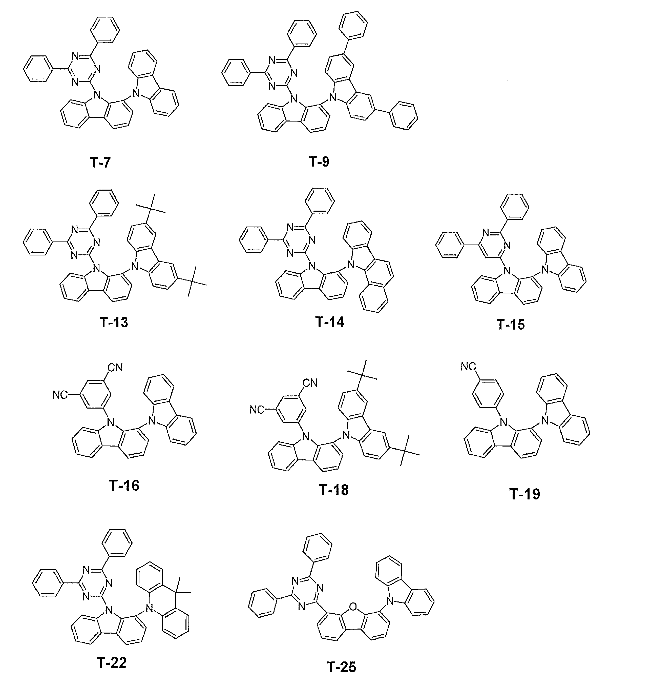
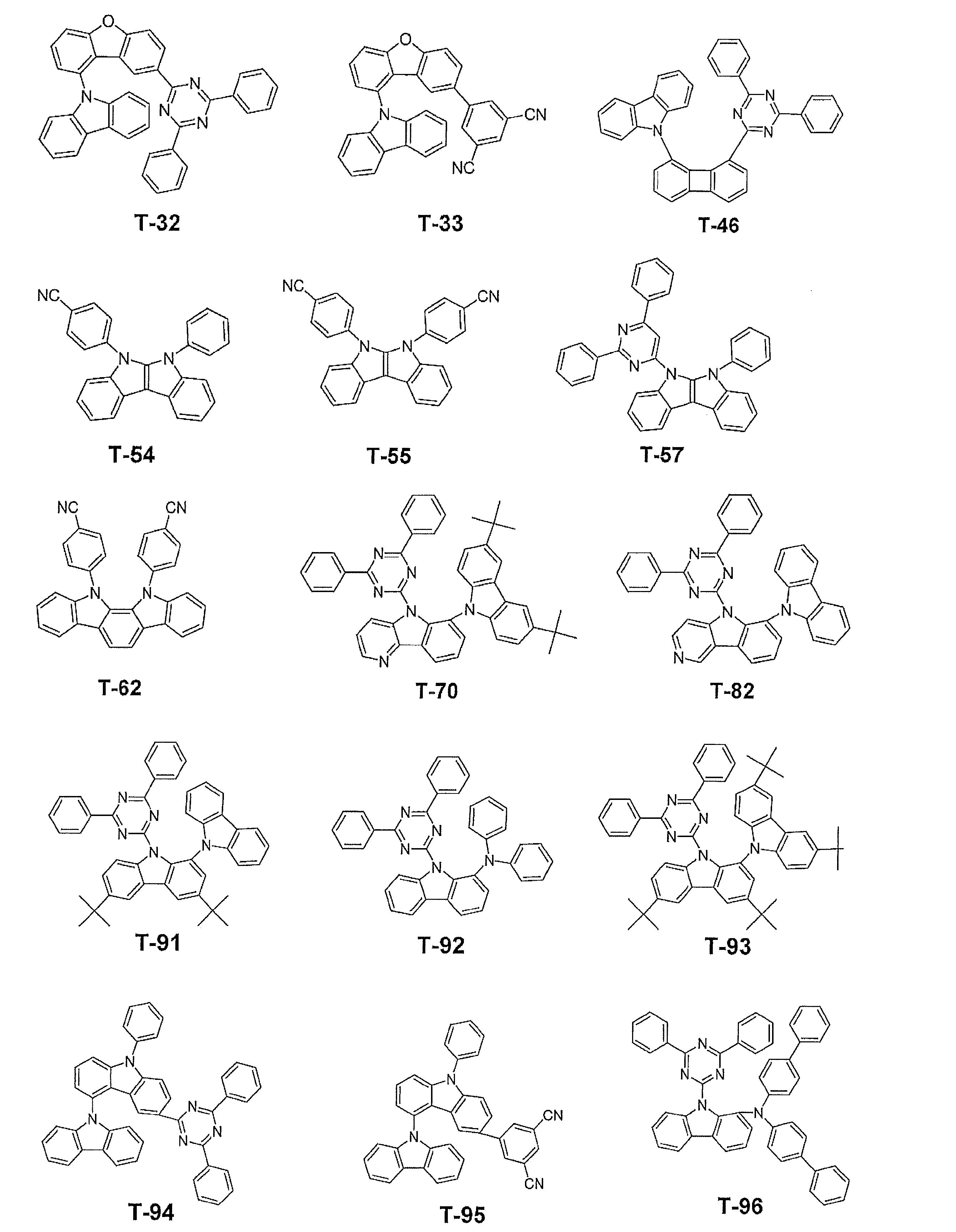

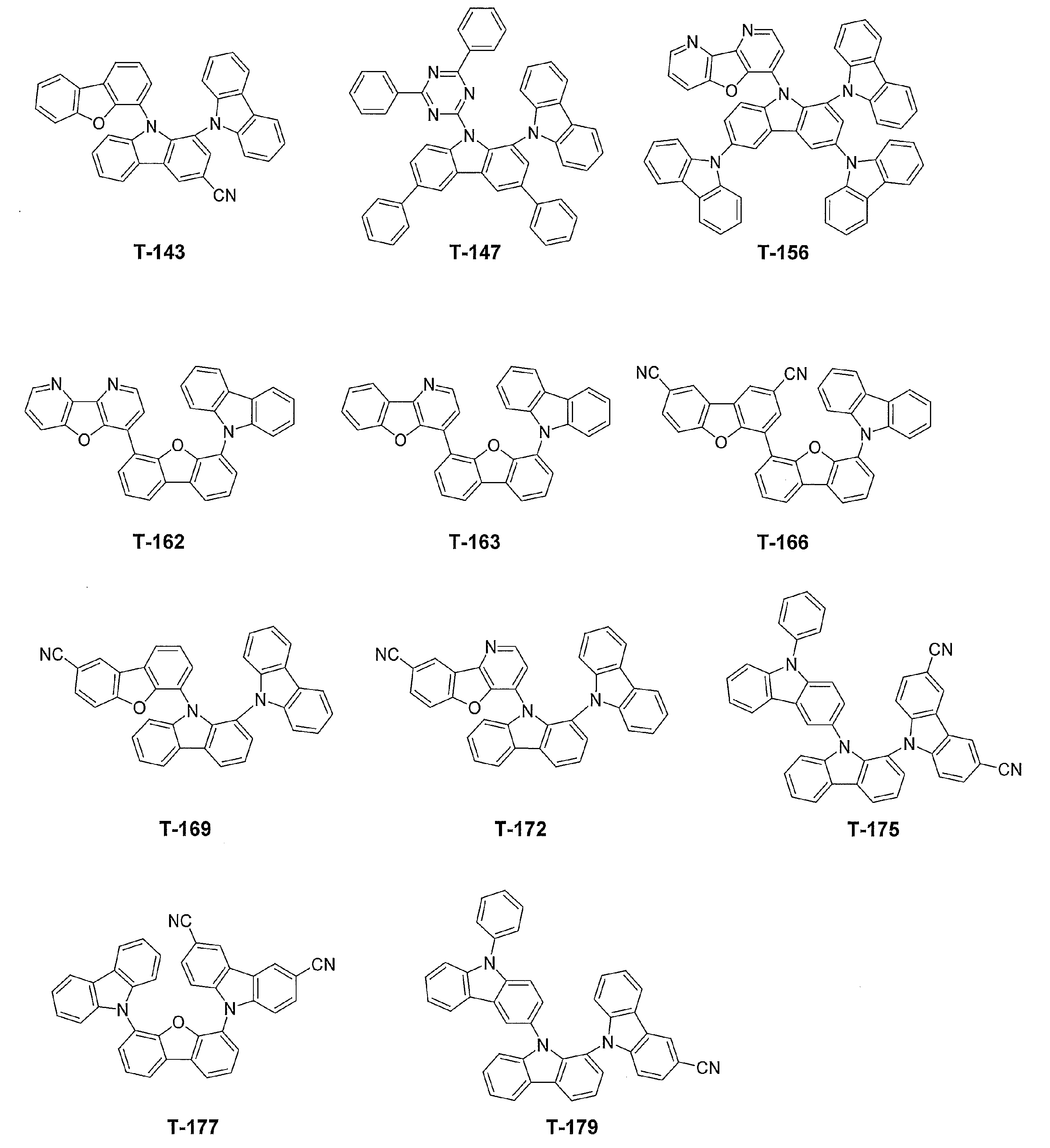

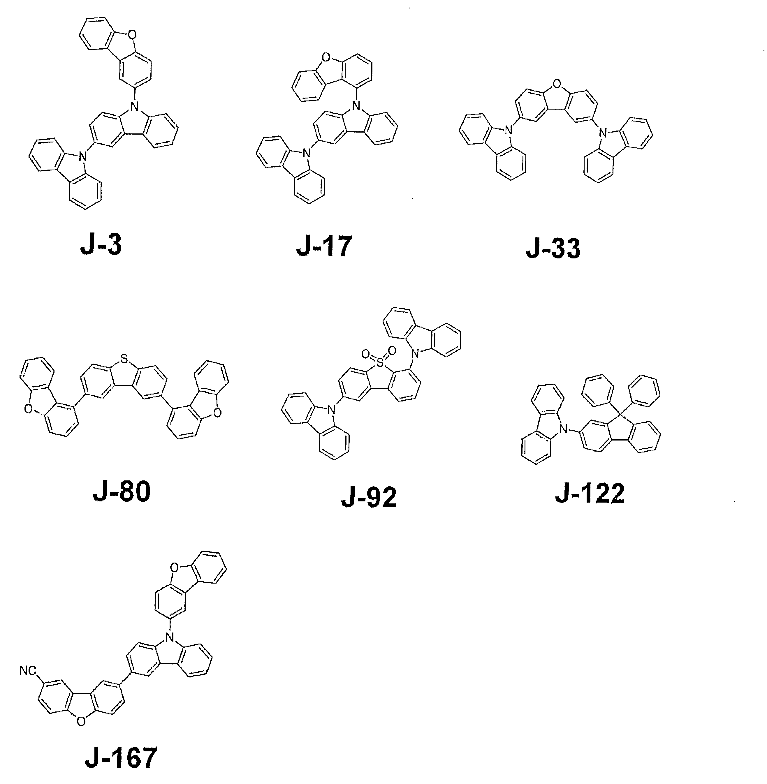
(π共役系化合物T-14の合成)
Angew. Chem. Int. Ed.,2014,53,2701.に記載の方法で合成した11H-ベンゾ[a]カルバゾールと、1-フルオロ-2-ニトロベンゼンとを、水素化ナトリウム存在下でN,N-ジメチルホルムアミド中、120℃で反応させ、11-(2-ニトロフェニル)-11H-ベンゾ[a]カルバゾールを得た。次に、11-(2-ニトロフェニル)-11H-ベンゾ[a]カルバゾールを塩化スズ存在下、エタノール中、80℃で加熱し、2-(11H-ベンゾ[a]カルバゾリル-11-イル)アニリンを得た。続いて、2-(11H-ベンゾ[a]カルバゾリル-11-イル)アニリンと1-ブロモ-2-ヨードベンゼンを、酢酸パラジウムとビス[2-(ジフェニルホスフィノ)フェニル]エーテルとt-ブトキシナトリウムの存在下、トルエン中、100℃で加熱し、N-(2-(11H-ベンゾ[a]カルバゾリル-11-イル)フェニル)-2-ブロモアニリンを得た。続いて、N-(2-(11H-ベンゾ[a]カルバゾリル-11-イル)フェニル)-2-ブロモアニリンを、酢酸パラジウムと1,1’-ビス(ジフェニルホスフィノ)フェロセンと炭酸カリウムの存在下、N,N-ジメチルホルムアミド中、140℃で反応させ、11-(9H-カルバゾリル-1-イル)-11H-ベンゾ[a]カルバゾールを得た。最後に、11-(9H-カルバゾリル-1-イル)-11H-ベンゾ[a]カルバゾールと2-クロロ-4,6-ジフェニル-1,3,5-トリアジンを、水素化ナトリウム存在下でN,N-ジメチルホルムアミド中、60℃で反応させ、π共役系化合物T-14の粗精製物を得た。その後、カラムクロマトグラフィー、再結晶、昇華精製を行って、π共役系化合物T-14の高純度品を取得した。
Angew. Chem. Int. Ed.,2014,53,2701.に記載の方法で合成した11H-ベンゾ[a]カルバゾールと、1-フルオロ-2-ニトロベンゼンとを、水素化ナトリウム存在下でN,N-ジメチルホルムアミド中、120℃で反応させ、11-(2-ニトロフェニル)-11H-ベンゾ[a]カルバゾールを得た。次に、11-(2-ニトロフェニル)-11H-ベンゾ[a]カルバゾールを塩化スズ存在下、エタノール中、80℃で加熱し、2-(11H-ベンゾ[a]カルバゾリル-11-イル)アニリンを得た。続いて、2-(11H-ベンゾ[a]カルバゾリル-11-イル)アニリンと1-ブロモ-2-ヨードベンゼンを、酢酸パラジウムとビス[2-(ジフェニルホスフィノ)フェニル]エーテルとt-ブトキシナトリウムの存在下、トルエン中、100℃で加熱し、N-(2-(11H-ベンゾ[a]カルバゾリル-11-イル)フェニル)-2-ブロモアニリンを得た。続いて、N-(2-(11H-ベンゾ[a]カルバゾリル-11-イル)フェニル)-2-ブロモアニリンを、酢酸パラジウムと1,1’-ビス(ジフェニルホスフィノ)フェロセンと炭酸カリウムの存在下、N,N-ジメチルホルムアミド中、140℃で反応させ、11-(9H-カルバゾリル-1-イル)-11H-ベンゾ[a]カルバゾールを得た。最後に、11-(9H-カルバゾリル-1-イル)-11H-ベンゾ[a]カルバゾールと2-クロロ-4,6-ジフェニル-1,3,5-トリアジンを、水素化ナトリウム存在下でN,N-ジメチルホルムアミド中、60℃で反応させ、π共役系化合物T-14の粗精製物を得た。その後、カラムクロマトグラフィー、再結晶、昇華精製を行って、π共役系化合物T-14の高純度品を取得した。
(その他のπ共役系化合物の合成)
前述と同様にして、π共役系化合物T-7、T-9、T-13、T-15、T-16、T-18、T-19、T-22、T-25、T-32、T-33、T-46、T-54、T-55、T-57、T-62、T-70、T-82、T-91、T-92、T-93、T-94、T-95、T-96、T-97、T-98、T-99、T-100、T-101、T-102、T-103、T-104、T-105、T-106、T-107、T-108、T-130、T-131、およびT-133を合成した。
前述と同様にして、π共役系化合物T-7、T-9、T-13、T-15、T-16、T-18、T-19、T-22、T-25、T-32、T-33、T-46、T-54、T-55、T-57、T-62、T-70、T-82、T-91、T-92、T-93、T-94、T-95、T-96、T-97、T-98、T-99、T-100、T-101、T-102、T-103、T-104、T-105、T-106、T-107、T-108、T-130、T-131、およびT-133を合成した。
得られたπ共役系化合物及び比較化合物1及び2のΔESTを、以下の方法で計算して求めた。
(ΔESTの算出)
化合物の分子軌道計算による構造最適化及び電子密度分布の算出は、計算手法として、汎関数としてB3LYP、基底関数として6-31G(d)を用いた分子軌道計算用ソフトウェアを用いて算出した。分子軌道計算用ソフトウェアとして、米国Gaussian社製のGaussian09(Revision C.01,M.J.Frisch,et al,Gaussian,Inc.,2010.)を用いた。
この汎関数としてB3LYP、基底関数として6-31G(d)を用いた構造最適化計算から、さらに時間依存密度汎関数法(Time-Dependent DFT)による励起状態計算を実施してS1、T1のエネルギー準位(それぞれE(S1)、E(T1))を求めてΔEST=|E(S1)-E(T1)|として算出した。
化合物の分子軌道計算による構造最適化及び電子密度分布の算出は、計算手法として、汎関数としてB3LYP、基底関数として6-31G(d)を用いた分子軌道計算用ソフトウェアを用いて算出した。分子軌道計算用ソフトウェアとして、米国Gaussian社製のGaussian09(Revision C.01,M.J.Frisch,et al,Gaussian,Inc.,2010.)を用いた。
この汎関数としてB3LYP、基底関数として6-31G(d)を用いた構造最適化計算から、さらに時間依存密度汎関数法(Time-Dependent DFT)による励起状態計算を実施してS1、T1のエネルギー準位(それぞれE(S1)、E(T1))を求めてΔEST=|E(S1)-E(T1)|として算出した。
[実施例1]
(有機EL素子1-1の作製)
50mm×50mm、厚さ0.7mmのガラス基板上に、陽極としてITO(インジウム・スズ酸化物)を150nmの厚さで成膜し、パターニングを行った後、このITO透明電極を付けた透明基板をイソプロピルアルコールで超音波洗浄し、乾燥窒素ガスで乾燥し、UVオゾン洗浄を5分間行った後、この透明基板を市販の真空蒸着装置の基板ホルダーに固定した。
真空蒸着装置内の蒸着用るつぼの各々に、各層の構成材料を、各々素子作製に最適の量を充填した。蒸着用るつぼはモリブデン製またはタングステン製の抵抗加熱用材料で作製されたものを用いた。
(有機EL素子1-1の作製)
50mm×50mm、厚さ0.7mmのガラス基板上に、陽極としてITO(インジウム・スズ酸化物)を150nmの厚さで成膜し、パターニングを行った後、このITO透明電極を付けた透明基板をイソプロピルアルコールで超音波洗浄し、乾燥窒素ガスで乾燥し、UVオゾン洗浄を5分間行った後、この透明基板を市販の真空蒸着装置の基板ホルダーに固定した。
真空蒸着装置内の蒸着用るつぼの各々に、各層の構成材料を、各々素子作製に最適の量を充填した。蒸着用るつぼはモリブデン製またはタングステン製の抵抗加熱用材料で作製されたものを用いた。
真空度1×10⁻⁴Paまで減圧した後、HI-1の入った蒸着用るつぼに通電して加熱し、蒸着速度0.1nm/秒でITO透明電極上に蒸着し、層厚10nmの正孔注入輸送層を形成した。
次いで、α-NPD(4,4’-ビス〔N-(1-ナフチル)-N-フェニルアミノ〕ビフェニル)を蒸着速度0.1nm/秒で前記正孔注入層上に蒸着し、層厚40nmの正孔輸送層を形成した。ホスト化合物としてH-232と発光性化合物として比較化合物1とを、それぞれ94%と6%の体積%になるように蒸着速度0.1nm/秒で共蒸着し、層厚30nmの発光層を形成した。
その後、BCP(2,9-ジメチル-4,7-ジフェニル-1,10-フェナントロリン)を蒸着速度0.1nm/秒で蒸着し、層厚30nmの電子輸送層を形成した。
さらに、フッ化リチウムを膜厚0.5nmで形成した後に、アルミニウム100nmを蒸着して陰極を形成した。
上記素子の非発光面側を、純度99.999%以上の高純度窒素ガスの雰囲気下で、缶状ガラスケースで覆い、電極取り出し配線を設置して、有機EL素子1-1を作製した。
次いで、α-NPD(4,4’-ビス〔N-(1-ナフチル)-N-フェニルアミノ〕ビフェニル)を蒸着速度0.1nm/秒で前記正孔注入層上に蒸着し、層厚40nmの正孔輸送層を形成した。ホスト化合物としてH-232と発光性化合物として比較化合物1とを、それぞれ94%と6%の体積%になるように蒸着速度0.1nm/秒で共蒸着し、層厚30nmの発光層を形成した。
その後、BCP(2,9-ジメチル-4,7-ジフェニル-1,10-フェナントロリン)を蒸着速度0.1nm/秒で蒸着し、層厚30nmの電子輸送層を形成した。
さらに、フッ化リチウムを膜厚0.5nmで形成した後に、アルミニウム100nmを蒸着して陰極を形成した。
上記素子の非発光面側を、純度99.999%以上の高純度窒素ガスの雰囲気下で、缶状ガラスケースで覆い、電極取り出し配線を設置して、有機EL素子1-1を作製した。
(有機EL素子1-2~1-42の作製)
発光性化合物を比較化合物1から表1に示すように変えた以外は、有機EL素子1-1と同様の方法で有機EL素子1-2から1-42を作製した。
発光性化合物を比較化合物1から表1に示すように変えた以外は、有機EL素子1-1と同様の方法で有機EL素子1-2から1-42を作製した。
(発光効率の測定)
作製した各有機EL素子について、駆動時の各サンプルの発光効率は下記測定を行うことにより評価した。
上記で作製した各有機EL素子を、室温(約25℃)、2.5mA/cm2の定電流条件下で発光させ、発光開始直後の発光輝度を、分光放射輝度計CS-2000(コニカミノルタ社製)を用いて測定した。
作製した各有機EL素子について、駆動時の各サンプルの発光効率は下記測定を行うことにより評価した。
上記で作製した各有機EL素子を、室温(約25℃)、2.5mA/cm2の定電流条件下で発光させ、発光開始直後の発光輝度を、分光放射輝度計CS-2000(コニカミノルタ社製)を用いて測定した。
(相対発光効率の算出)
得られた発光輝度の相対値(実施例1では有機EL素子1-1の発光輝度に対する相対値)を求め、表1に示した。
得られた発光輝度の相対値(実施例1では有機EL素子1-1の発光輝度に対する相対値)を求め、表1に示した。
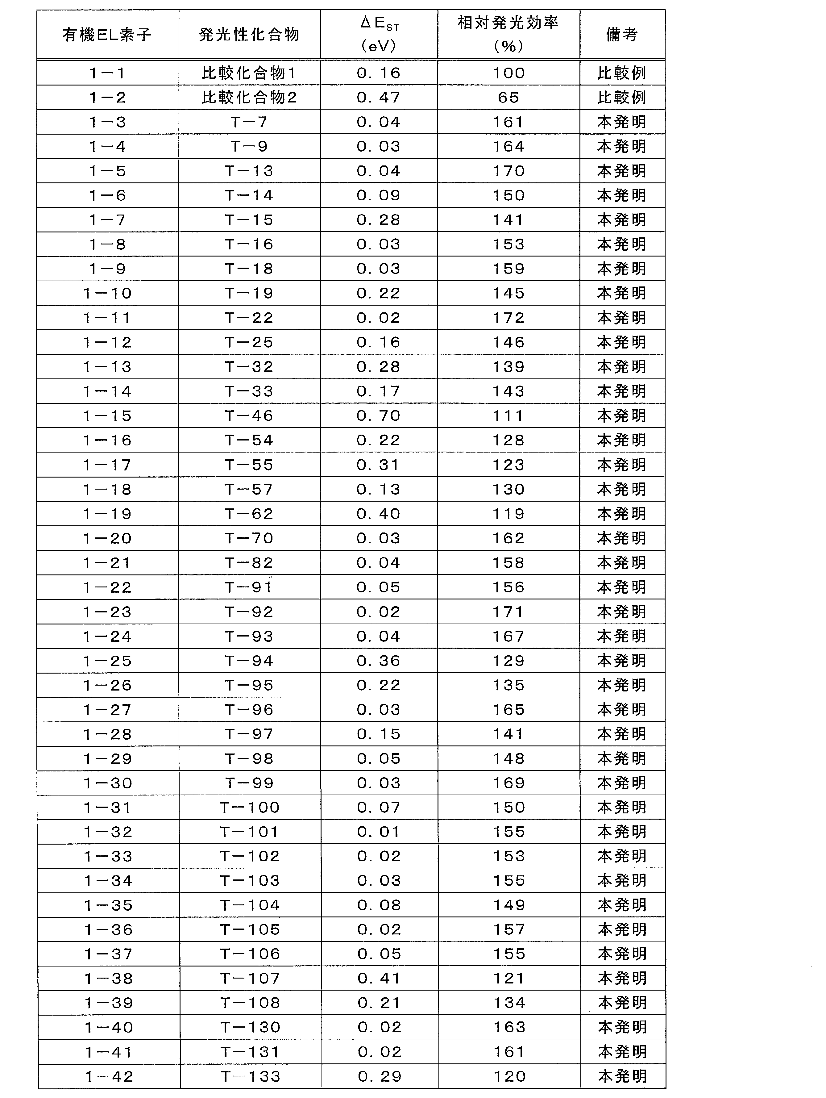
表1から明らかなように、発光性化合物として比較化合物よりも本発明の化合物を使用した有機EL素子の方が、高い発光効率を示した。特に化合物T-7、T-9、T-13、T-14、T-16、T-18、T-22、T-70、T-82、T-91、T-92、T-93、T-96、T-98、T-99、T-100、T-101、T-102、T-103、T-104、T-105、T-106、T-130及びT-131を用いた有機EL素子は、ΔESTの絶対値が0.1未満であり、且つ相対発光効率も148%以上と高かった。
[実施例2]
(有機EL素子2-1の作製)
陽極として100mm×100mm×1.1mmのガラス基板上にITO(インジウムチンオキシド)を100nm成膜した基板(NHテクノグラス社製NA45)にパターニングを行った後、このITO透明電極を設けた透明支持基板をイソプロピルアルコールで超音波洗浄し、乾燥窒素ガスで乾燥し、UVオゾン洗浄を5分間行った。
この透明支持基板上に、ポリ(3,4-エチレンジオキシチオフェン)-ポリスチレンスルホネート(PEDOT/PSS、Bayer社製、Baytron P Al 4083)を純水で70%に希釈した溶液を用いて3000rpm、30秒の条件下、スピンコート法により薄膜を形成した後、200℃にて1時間乾燥し、層厚20nmの正孔注入層を設けた。この透明支持基板を市販の真空蒸着装置の基板ホルダーに固定し、真空蒸着装置内の蒸着用るつぼの各々に、各層の構成材料を、各々素子作製に最適の量を充填した。蒸着用るつぼはモリブデン製またはタングステン製の抵抗加熱用材料で作製されたものを用いた。
(有機EL素子2-1の作製)
陽極として100mm×100mm×1.1mmのガラス基板上にITO(インジウムチンオキシド)を100nm成膜した基板(NHテクノグラス社製NA45)にパターニングを行った後、このITO透明電極を設けた透明支持基板をイソプロピルアルコールで超音波洗浄し、乾燥窒素ガスで乾燥し、UVオゾン洗浄を5分間行った。
この透明支持基板上に、ポリ(3,4-エチレンジオキシチオフェン)-ポリスチレンスルホネート(PEDOT/PSS、Bayer社製、Baytron P Al 4083)を純水で70%に希釈した溶液を用いて3000rpm、30秒の条件下、スピンコート法により薄膜を形成した後、200℃にて1時間乾燥し、層厚20nmの正孔注入層を設けた。この透明支持基板を市販の真空蒸着装置の基板ホルダーに固定し、真空蒸着装置内の蒸着用るつぼの各々に、各層の構成材料を、各々素子作製に最適の量を充填した。蒸着用るつぼはモリブデン製またはタングステン製の抵抗加熱用材料で作製されたものを用いた。
真空度1×10⁻⁴Paまで減圧した後、α-NPDを蒸着速度0.1nm/秒で前記正孔注入層上に蒸着し、層厚40nmの正孔輸送層を形成した。ホスト化合物としてH-234と、発光性化合物として2,5,8,11-テトラ-t-ブチルペリレンとが、それぞれ97%と3%の体積%になるように蒸着速度0.1nm/秒で共蒸着し、層厚30nmの発光層を形成した。
その後、TPBi(1,3,5-トリス(N-フェニルベンゾイミダゾール-2-イル)を蒸着速度0.1nm/秒で蒸着し、層厚30nmの電子輸送層を形成した。
さらに、フッ化ナトリウムを膜厚1nmで形成した後に、アルミニウム100nmを蒸着して陰極を形成した。
上記素子の非発光面側を、純度99.999%以上の高純度窒素ガスの雰囲気下で、缶状ガラスケースで覆い、電極取り出し配線を設置して、有機EL素子2-1を作製した。
その後、TPBi(1,3,5-トリス(N-フェニルベンゾイミダゾール-2-イル)を蒸着速度0.1nm/秒で蒸着し、層厚30nmの電子輸送層を形成した。
さらに、フッ化ナトリウムを膜厚1nmで形成した後に、アルミニウム100nmを蒸着して陰極を形成した。
上記素子の非発光面側を、純度99.999%以上の高純度窒素ガスの雰囲気下で、缶状ガラスケースで覆い、電極取り出し配線を設置して、有機EL素子2-1を作製した。
(有機EL素子2-2の作製)
ホスト化合物としてH-234、発光性化合物として2,5,8,11-テトラ-t-ブチルペリレン、第三成分として比較化合物1を用い、それぞれの比率が82%、3%、15%の体積%となるように発光層を形成した以外は有機EL素子2-1の作製と同様にして、有機EL素子2-2を作製した。
ホスト化合物としてH-234、発光性化合物として2,5,8,11-テトラ-t-ブチルペリレン、第三成分として比較化合物1を用い、それぞれの比率が82%、3%、15%の体積%となるように発光層を形成した以外は有機EL素子2-1の作製と同様にして、有機EL素子2-2を作製した。
(有機EL素子2-3~2-13の作製)
表2に示すように第三成分を変えた以外は、有機EL素子2-2と同様の方法で有機EL素子2-3から2-13を作製した。
表2に示すように第三成分を変えた以外は、有機EL素子2-2と同様の方法で有機EL素子2-3から2-13を作製した。
作製した各有機EL素子について、駆動時の各サンプルの発光効率を実施例1と同様にして測定した。得られた発光輝度の相対値(実施例2では有機EL素子2-1の発光輝度に対する相対値)を求め、表2に示した。

表2から明らかなように、第三成分として比較例化合物よりも本発明の化合物を使用した有機EL素子の方が、高い発光効率を示した。特に化合物T-9、T-13、T-18、T-22、T-91、T-99、T-105及びT-131を用いた有機EL素子は、ΔESTの絶対値が0.1未満であり、且つ相対発光効率も149%以上と高かった。
[実施例3]
(有機EL素子3-1の作製)
50mm×50mm、厚さ0.7mmのガラス基板上に、陽極としてITO(インジウム・スズ酸化物)を150nmの厚さで製膜し、パターニングを行った後、このITO透明電極を付けた透明基板をイソプロピルアルコールで超音波洗浄し、乾燥窒素ガスで乾燥し、UVオゾン洗浄を5分間行った後、この透明基板を市販の真空蒸着装置の基板ホルダーに固定した。
(有機EL素子3-1の作製)
50mm×50mm、厚さ0.7mmのガラス基板上に、陽極としてITO(インジウム・スズ酸化物)を150nmの厚さで製膜し、パターニングを行った後、このITO透明電極を付けた透明基板をイソプロピルアルコールで超音波洗浄し、乾燥窒素ガスで乾燥し、UVオゾン洗浄を5分間行った後、この透明基板を市販の真空蒸着装置の基板ホルダーに固定した。
真空蒸着装置内の蒸着用の抵抗加熱ボートの各々に、各層の構成材料を、各々素子作製に最適の量を充填した。前記抵抗加熱ボートはモリブデン製又はタングステン製を用いた。
真空度1×10⁻⁴Paまで減圧した後、HI-1の入った抵抗加熱ボートに通電して加熱し、蒸着速度0.1nm/秒でITO透明電極上に蒸着し、層厚15nmの正孔注入層を形成した。
次いで、α-NPD(4,4’-ビス〔N-(1-ナフチル)-N-フェニルアミノ〕ビフェニル)を蒸着速度0.1nm/秒で蒸着し、層厚30nmの正孔輸送層を形成した。
次いで、比較のホスト化合物として比較化合物1と発光性化合物としてGD-1とが入った抵抗加熱ボートに通電して加熱し、それぞれ蒸着速度0.1nm/秒、0.010nm/秒で前記正孔輸送層上に共蒸着し、層厚40nmの発光層を形成した。
次いで、HB-1を蒸着速度0.1nm/秒で蒸着し、層厚5nmの第一電子輸送層を形成した。
さらにその上に、ET―1を蒸着速度0.1nm/秒で蒸着し、層厚45nmの第二電子輸送層を形成した。
その後、フッ化リチウムを厚さ0.5nmになるよう蒸着した後に、アルミニウム100nmを蒸着して陰極を形成し、有機EL素子3-1を作製した。
(有機EL素子3-2~3-24の作製)
ホスト化合物を比較化合物1から表3に示すように変えた以外は、有機EL素子3-1と同様の方法で有機EL素子3-2から3-24を作製した。
ホスト化合物を比較化合物1から表3に示すように変えた以外は、有機EL素子3-1と同様の方法で有機EL素子3-2から3-24を作製した。
作製した各有機EL素子について、駆動時の各サンプルの発光効率を実施例1と同様にして測定した。得られた発光輝度の相対値(実施例3では有機EL素子3-1の発光輝度に対する相対値)を求め、表3に示した。

表3から明らかなように、ホスト化合物として比較例化合物よりも本発明の化合物を使用した有機EL素子の方が、高い発光効率を示した。特に化合物T-13、T-16、T-82、T-100、T-103、T-105、T-147、T-156及びT-172を用いた有機EL素子は、ΔESTの絶対値が0.1未満であり、且つ相対発光効率も145%以上と高かった。
[実施例4]
(有機EL素子4-1の作製)
50mm×50mm、厚さ0.7mmのガラス基板上に、陽極としてITO(インジウム・スズ酸化物)を150nmの厚さで製膜し、パターニングを行った後、このITO透明電極を付けた透明基板をイソプロピルアルコールで超音波洗浄し、乾燥窒素ガスで乾燥し、UVオゾン洗浄を5分間行った後、この透明基板を市販の真空蒸着装置の基板ホルダーに固定した。
(有機EL素子4-1の作製)
50mm×50mm、厚さ0.7mmのガラス基板上に、陽極としてITO(インジウム・スズ酸化物)を150nmの厚さで製膜し、パターニングを行った後、このITO透明電極を付けた透明基板をイソプロピルアルコールで超音波洗浄し、乾燥窒素ガスで乾燥し、UVオゾン洗浄を5分間行った後、この透明基板を市販の真空蒸着装置の基板ホルダーに固定した。
真空蒸着装置内の蒸着用の抵抗加熱ボートの各々に、各層の構成材料を、各々素子作製に最適の量を充填した。前記抵抗加熱ボートはモリブデン製又はタングステン製を用いた。
真空度1×10⁻⁴Paまで減圧した後、α-NPD(4,4’-ビス〔N-(1-ナフチル)-N-フェニルアミノ〕ビフェニル)の入った抵抗加熱ボートに通電して加熱し、蒸着速度0.1nm/秒でITO透明電極上に蒸着し、層厚30nmの正孔注入層を形成した。
次いで、TCTA(トリス(4-カルバゾイル-9-イルフェニル)アミン)を蒸着速度0.1nm/秒で蒸着し、層厚20nmの第一正孔輸送層を形成した。
さらに、H-233を蒸着速度0.1nm/秒で蒸着し、層厚10nmの第二正孔輸送層を形成した。
次いで、比較のホスト化合物である比較化合物1とTBPe(2,5,8,11-テトラ-tert-ブチルペリレン)の入った抵抗加熱ボートに通電して加熱し、それぞれ蒸着速度0.1nm/秒、0.010nm/秒で前記正孔輸送層上に共蒸着し、層厚20nmの発光層を形成した。
次いで、H-232を蒸着速度0.1nm/秒で蒸着し、層厚10nmの第一電子輸送層を形成した。
さらにその上に、TBPI(1,3,5-トリス(1-フェニル-1H-ベンズイミダゾール-2-イル)ベンゼン)を蒸着速度0.1nm/秒で蒸着し、層厚30mの第二電子輸送層を形成した。
その後、フッ化リチウムを厚さ0.5nmになるよう蒸着した後に、アルミニウム100nmを蒸着して陰極を形成し、有機EL素子4-1を作製した。
(有機EL素子4-2~4-12の作製)
ホスト化合物を比較化合物1から表4に示すように変えた以外は、有機EL素子4-1と同様の方法で有機EL素子4-2から4-12を作製した。
ホスト化合物を比較化合物1から表4に示すように変えた以外は、有機EL素子4-1と同様の方法で有機EL素子4-2から4-12を作製した。
作製した各有機EL素子について、駆動時の各サンプルの発光効率を実施例1と同様にして測定した。得られた発光輝度の相対値(実施例4では有機EL素子4-1の発光輝度に対する相対値)を求め、表4に示した。
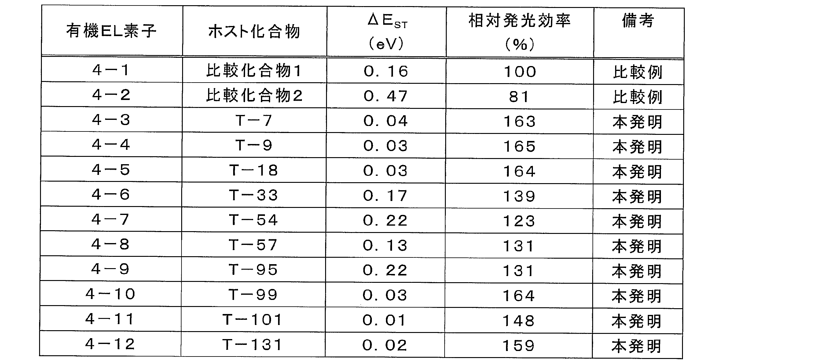
表4から明らかなように、ホスト化合物として比較例化合物よりも本発明の化合物を使用した有機EL素子の方が、高い発光効率を示した。特に化合物T-7、T-9、T-18、T-99、T-101及びT-131を用いた有機EL素子は、ΔESTの絶対値が0.1未満であり、且つ相対発光効率も148%以上と高かった。
[実施例5]
有機EL素子を初期輝度300cd/m2で点灯した時の、輝度半減時間を測定した。
有機EL素子を初期輝度300cd/m2で点灯した時の、輝度半減時間を測定した。
(有機EL素子5-1~5-7の作製)
ホスト化合物および発光性化合物を表5に示すように変えた以外は、実施例1の有機EL素子1-4と同様の方法で、有機EL素子5-1から5-7を作製した。
ホスト化合物および発光性化合物を表5に示すように変えた以外は、実施例1の有機EL素子1-4と同様の方法で、有機EL素子5-1から5-7を作製した。
(相対輝度半減時間の測定)
上記で作製した有機EL素子5-1から5-7と、実施例1で作製した有機EL素子1-4、1-5、1-12、1-13、1-16、1-40と1-42について、相対輝度半減時間を測定した。具体的には、各有機EL素子の輝度が300cd/m2となる条件で点灯し、その輝度が半分の150cd/m2となるまでに要する時間を測定し、輝度半減時間を得た。得られた輝度半減時間の相対値(有機EL素子1-16の輝度半減時間に対する相対値)を求め、表5に示した。
上記で作製した有機EL素子5-1から5-7と、実施例1で作製した有機EL素子1-4、1-5、1-12、1-13、1-16、1-40と1-42について、相対輝度半減時間を測定した。具体的には、各有機EL素子の輝度が300cd/m2となる条件で点灯し、その輝度が半分の150cd/m2となるまでに要する時間を測定し、輝度半減時間を得た。得られた輝度半減時間の相対値(有機EL素子1-16の輝度半減時間に対する相対値)を求め、表5に示した。

表5から明らかなように、ホスト化合物が前述の一般式(I)で表される化合物である実施例5の有機EL素子は、同じ発光性化合物を用いるが、他のホスト化合物を用いた実施例1の有機EL素子と比べて、10倍以上の長い相対輝度半減時間を示した。
[実施例6]
(共蒸着膜6-1の作製)
50mm×50mm、厚さ0.7mmの石英基板をイソプロピルアルコールで超音波洗浄し、乾燥窒素ガスで乾燥し、UVオゾン洗浄を5分間行った後、この透明基板を市販の真空蒸着装置の基板ホルダーに固定した。
真空蒸着装置内の蒸着用るつぼの各々に、H-232および発光性化合物T-14を充填した。蒸着用るつぼはモリブデン製またはタングステン製の抵抗加熱用材料で作製されたものを用いた。
真空度1×10⁻⁴Paまで減圧した後、H-232と発光性化合物T-14を、それぞれ94%と6%の体積%になるように蒸着速度0.1nm/秒で共蒸着し、層厚40nmの共蒸着膜5-1を形成した。
(共蒸着膜6-1の作製)
50mm×50mm、厚さ0.7mmの石英基板をイソプロピルアルコールで超音波洗浄し、乾燥窒素ガスで乾燥し、UVオゾン洗浄を5分間行った後、この透明基板を市販の真空蒸着装置の基板ホルダーに固定した。
真空蒸着装置内の蒸着用るつぼの各々に、H-232および発光性化合物T-14を充填した。蒸着用るつぼはモリブデン製またはタングステン製の抵抗加熱用材料で作製されたものを用いた。
真空度1×10⁻⁴Paまで減圧した後、H-232と発光性化合物T-14を、それぞれ94%と6%の体積%になるように蒸着速度0.1nm/秒で共蒸着し、層厚40nmの共蒸着膜5-1を形成した。
(共蒸着膜6-1の遅延蛍光の測定)
窒素雰囲気下で、共蒸着膜6-1に355nmの励起光を照射し、極大発光波長での蛍光減衰測定を行った。
共蒸着膜6-1について、時間と光子数との関係を示すグラフを図11に示す。
窒素雰囲気下で、共蒸着膜6-1に355nmの励起光を照射し、極大発光波長での蛍光減衰測定を行った。
共蒸着膜6-1について、時間と光子数との関係を示すグラフを図11に示す。
図11に示すように、本発明のπ共有化合物(T-14)は、蛍光の減衰速度の異なる成分が2種以上確認され、遅延蛍光を放射することが確認された。
本出願は、2015年12月28日出願の特願2015-256970に基づく優先権を主張する。当該出願明細書および図面に記載された内容は、すべて本願明細書に援用される。
本発明によれば、有機エレクトロルミネッセンス素子の発光効率を改良しうる新たなπ共役系化合物を提供することができる。また、当該π共役系化合物を用いた有機エレクトロルミネッセンス素子材料、発光材料、電荷輸送材料、発光性薄膜、有機エレクトロルミネッセンス素子、表示装置及び照明装置を提供することができる。
1 ディスプレイ
3 画素
5 走査線
6 データ線
7 電源ライン
10 有機EL素子
11 スイッチングトランジスタ
12 駆動トランジスタ
13 コンデンサー
101 照明装置内の有機EL素子
102 ガラスカバー
105 陰極
106 有機層
107 透明電極付きガラス基板
108 窒素ガス
109 捕水剤
A 表示部
B 制御部
C 配線部
3 画素
5 走査線
6 データ線
7 電源ライン
10 有機EL素子
11 スイッチングトランジスタ
12 駆動トランジスタ
13 コンデンサー
101 照明装置内の有機EL素子
102 ガラスカバー
105 陰極
106 有機層
107 透明電極付きガラス基板
108 窒素ガス
109 捕水剤
A 表示部
B 制御部
C 配線部
Claims (22)
- 下記一般式(1)~(6)のいずれか1つで表される構造を有する、π共役系化合物。
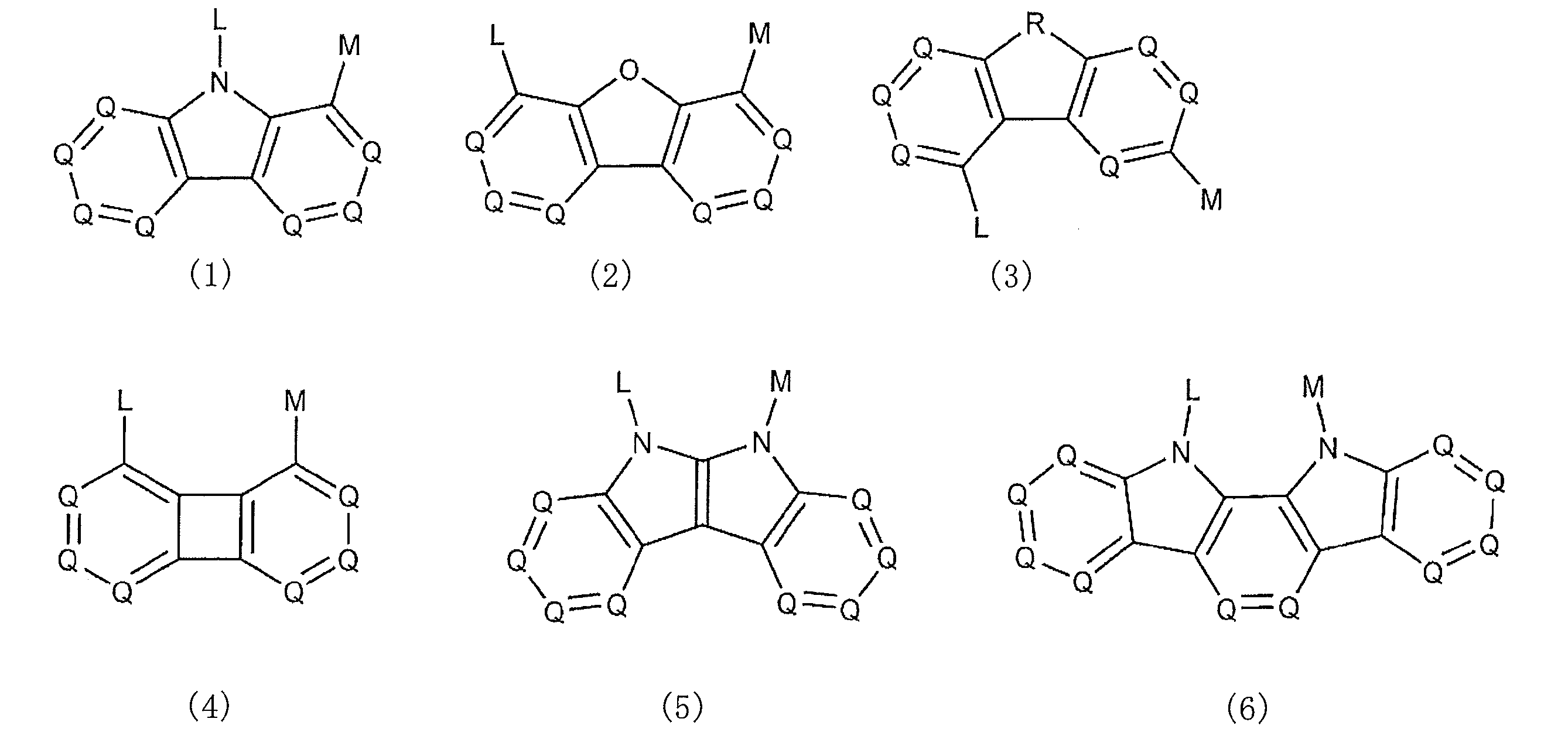
LとMは各々独立に、電子供与性基D又は電子求引性基Aを表し、
前記電子供与性基Dは、電子供与性基で置換されたアリール基、置換されていてもよい電子供与性基の複素環基、及び置換されていてもよいアミノ基からなる群より選ばれる基であり、
前記電子求引性基Aは、置換されていてもよいカルボニル基、置換されていてもよいスルホニル基、置換されていてもよいホスフィンオキサイド基、置換されていてもよいボリル基、電子求引性基で置換されていてもよいアリール基、電子求引性基で置換されている電子供与性の複素環基、及び置換されていてもよい電子求引性の複素環基からなる群より選ばれる基であり、
Qは各々独立に、炭素原子又は窒素原子を表し、
一般式(3)中、
Rは炭素原子、酸素原子、窒素原子、硫黄原子、ホウ素原子又はケイ素原子を表す。) - 一般式(1)~(6)において、前記LとMの一方が前記電子供与性基Dであり、他方が前記電子求引性基Aである、請求項1に記載のπ共役系化合物。
- 前記電子供与性基Dは、電子供与性基で置換されたアリール基又は置換されていてもよい電子供与性基の複素環基である、請求項1又は2に記載のπ共役系化合物。
- 前記電子求引性基Aは、電子求引性基で置換されていてもよいアリール基、電子求引性基で置換されている電子供与性の複素環基、又は置換されていてもよい電子求引性の複素環基である、請求項1~3のいずれか一項に記載のπ共役系化合物。
- 最低励起一重項準位と最低励起三重項準位とのエネルギー差の絶対値ΔESTが0.50eV以下である、請求項1~4のいずれか一項に記載のπ共役系化合物。
- 請求項1~5のいずれか一項に記載のπ共役系化合物を含む、有機エレクトロルミネッセンス素子材料。
- 請求項1~5のいずれか一項に記載のπ共役系化合物を含み、前記π共役系化合物が蛍光を放射する、発光材料。
- 前記π共役系化合物が、遅延蛍光を放射する、請求項7に記載の発光材料。
- 請求項1~5のいずれか一項に記載のπ共役系化合物を含み、前記π共役系化合物が遅延蛍光を放射する、電荷輸送材料。
- 請求項1~5のいずれか一項に記載のπ共役系化合物を含む、発光性薄膜。
- 前記π共役系化合物が、遅延蛍光を放射する、請求項10に記載の発光性薄膜。
- 陽極と、陰極と、前記陽極と前記陰極との間に設けられた発光層とを含み、
前記発光層の少なくとも一層が、請求項1~5のいずれか一項に記載のπ共役系化合物を含む、有機エレクトロルミネッセンス素子。 - 前記π共役系化合物が、励起子を生成する、請求項12に記載の有機エレクトロルミネッセンス素子。
- 前記π共役系化合物が、蛍光を放射する、請求項12又は13に記載の有機エレクトロルミネッセンス素子。
- 前記π共役系化合物が、遅延蛍光を放射する、請求項14に記載の有機エレクトロルミネッセンス素子。
- 前記発光層が、前記π共役系化合物と、ホスト化合物と、を含む、請求項12~15のいずれか一項に記載の有機エレクトロルミネッセンス素子。
- 前記発光層は、前記π共役系化合物と、蛍光発光性化合物及びリン光発光性化合物の少なくとも一方とを含む、請求項12~16のいずれか一項に記載の有機エレクトロルミネッセンス素子。
- 前記発光層は、前記π共役系化合物と、蛍光発光性化合物及びリン光発光性化合物の少なくとも一方と、ホスト化合物とを含む、請求項12~16のいずれか一項に記載の有機エレクトロルミネッセンス素子。
- 前記ホスト化合物が、下記一般式(I)で表される構造を有する、請求項16又は18に記載の有機エレクトロルミネッセンス素子。

X101は、NR101、酸素原子、硫黄原子、スルフィニル基、スルホニル基、CR102R103又はSiR104R105を表し、
y1~y8は、それぞれ独立に、CR106又は窒素原子を表し、
R101~R106は、それぞれ独立に、水素原子又は置換基を表し、互いに結合して環を形成してもよく、
Ar101及びAr102は、それぞれ独立に、置換されていてもよいアリール基、又は置換されていてもよいヘテロアリール基を表し、
n101及びn102は、各々0~4の整数を表す。
ただし、R101が水素原子の場合は、n101は1~4の整数を表す。) - 前記一般式(I)で表される構造を有するホスト化合物が、下記一般式(II)で表される構造を有する、請求項19に記載の有機エレクトロルミネッセンス素子。

X101は、NR101、酸素原子、硫黄原子、スルフィニル基、スルホニル基、CR102R103又はSiR104R105を表し、
R101~R105は、各々水素原子又は置換基を表し、互いに結合して環を形成してもよく、
Ar101及びAr102は、それぞれ独立に、置換されていてもよいアリール基、又は置換されていてもよいヘテロアリール基を表し、
n102は0~4の整数を表す。) - 請求項12~20のいずれか一項に記載の有機エレクトロルミネッセンス素子を含む、表示装置。
- 請求項12~20のいずれか一項に記載の有機エレクトロルミネッセンス素子を含む、照明装置。
Priority Applications (1)
| Application Number | Priority Date | Filing Date | Title |
|---|---|---|---|
| JP2017558903A JP6873048B2 (ja) | 2015-12-28 | 2016-12-02 | 有機エレクトロルミネッセンス素子、表示装置及び照明装置 |
Applications Claiming Priority (2)
| Application Number | Priority Date | Filing Date | Title |
|---|---|---|---|
| JP2015256970 | 2015-12-28 | ||
| JP2015-256970 | 2015-12-28 |
Publications (1)
| Publication Number | Publication Date |
|---|---|
| WO2017115608A1 true WO2017115608A1 (ja) | 2017-07-06 |
Family
ID=59227366
Family Applications (1)
| Application Number | Title | Priority Date | Filing Date |
|---|---|---|---|
| PCT/JP2016/085840 Ceased WO2017115608A1 (ja) | 2015-12-28 | 2016-12-02 | π共役系化合物、有機エレクトロルミネッセンス素子材料、発光材料、電荷輸送材料、発光性薄膜、有機エレクトロルミネッセンス素子、表示装置及び照明装置 |
Country Status (2)
| Country | Link |
|---|---|
| JP (2) | JP6873048B2 (ja) |
| WO (1) | WO2017115608A1 (ja) |
Cited By (18)
| Publication number | Priority date | Publication date | Assignee | Title |
|---|---|---|---|---|
| US20180166634A1 (en) * | 2016-12-14 | 2018-06-14 | Samsung Electronics Co., Ltd. | Organic light-emitting device and compound |
| CN109320449A (zh) * | 2017-08-01 | 2019-02-12 | 三星显示有限公司 | 杂环化合物以及包括该杂环化合物的有机电致发光装置 |
| WO2019078536A1 (ko) * | 2017-10-20 | 2019-04-25 | 삼성에스디아이 주식회사 | 유기 광전자 소자용 조성물, 유기 광전자 소자 및 표시 장치 |
| WO2019088751A1 (ko) * | 2017-11-03 | 2019-05-09 | 주식회사 엘지화학 | 화합물 및 이를 포함하는 유기 발광 소자 |
| JP2019073489A (ja) * | 2017-10-19 | 2019-05-16 | Dic株式会社 | 有機エレクトロルミネッセンス素子及び材料 |
| CN109761973A (zh) * | 2017-11-10 | 2019-05-17 | 三星显示有限公司 | 含氮化合物和包括该含氮化合物的有机电致发光装置 |
| CN109796473A (zh) * | 2017-11-16 | 2019-05-24 | 江苏三月光电科技有限公司 | 一种以吡啶并吲哚为核心的化合物及其应用 |
| KR20190068103A (ko) * | 2017-12-08 | 2019-06-18 | 엘지디스플레이 주식회사 | 내열 특성이 우수한 유기 화합물, 이를 포함하는 유기발광다이오드 및 유기발광장치 |
| CN110437133A (zh) * | 2019-07-18 | 2019-11-12 | 中国科学院上海微系统与信息技术研究所 | 一种长寿命室温磷光材料及其制备方法和应用 |
| CN110785416A (zh) * | 2017-11-03 | 2020-02-11 | 株式会社Lg化学 | 化合物及包含其的有机发光器件 |
| WO2021230214A1 (ja) * | 2020-05-13 | 2021-11-18 | コニカミノルタ株式会社 | 有機エレクトロルミネッセンス素子、その製造方法、それを具備した簡易表示装置及び印刷物 |
| WO2021230714A1 (ko) * | 2020-05-14 | 2021-11-18 | 주식회사 엘지화학 | 유기 발광 소자 |
| KR20210141402A (ko) * | 2020-05-14 | 2021-11-23 | 주식회사 엘지화학 | 유기 발광 소자 |
| JP2022520284A (ja) * | 2019-02-18 | 2022-03-29 | メルク パテント ゲーエムベーハー | 有機電子デバイス用の組成物 |
| WO2022075566A1 (ko) * | 2020-10-08 | 2022-04-14 | 엘티소재주식회사 | 헤테로고리 화합물, 이를 포함하는 유기 발광 소자, 이의 제조 방법 및 유기 발광 소자의 유기물층용 조성물 |
| WO2023078812A1 (de) | 2021-11-02 | 2023-05-11 | Merck Patent Gmbh | Benzofuro[3,2-d]pyrimidin-2,4-dicarbonitril-derivate und ähnliche verbindungen für organische elektrolumineszenzvorrichtungen |
| WO2024079356A1 (fr) * | 2022-10-14 | 2024-04-18 | Saint-Gobain Centre De Recherches Et D'etudes Europeen | Produit refractaire alumine-zircone-silice |
| WO2025125167A1 (de) | 2023-12-11 | 2025-06-19 | Merck Patent Gmbh | Materialien für organische elektrolumineszenzvorrichtungen |
Families Citing this family (3)
| Publication number | Priority date | Publication date | Assignee | Title |
|---|---|---|---|---|
| JP7838780B2 (ja) * | 2021-05-20 | 2026-04-01 | 株式会社Kyulux | 有機発光素子 |
| CN118923225A (zh) * | 2022-03-30 | 2024-11-08 | 索尼集团公司 | 发光元件和电子设备 |
| KR20240168760A (ko) * | 2023-05-23 | 2024-12-02 | 삼성에스디아이 주식회사 | 유기 광전자 소자용 조성물, 유기 광전자 소자 및 표시 장치 |
Citations (14)
| Publication number | Priority date | Publication date | Assignee | Title |
|---|---|---|---|---|
| WO2011070963A1 (ja) * | 2009-12-07 | 2011-06-16 | 新日鐵化学株式会社 | 有機発光材料及び有機発光素子 |
| JP2012049518A (ja) * | 2010-07-27 | 2012-03-08 | Konica Minolta Holdings Inc | 有機エレクトロルミネッセンス素子材料、化合物、有機エレクトロルミネッセンス素子、表示装置、並びに照明装置 |
| WO2012035853A1 (ja) * | 2010-09-13 | 2012-03-22 | 新日鐵化学株式会社 | 含窒素芳香族化合物、有機半導体材料及び有機電子デバイス |
| WO2013180097A1 (ja) * | 2012-05-28 | 2013-12-05 | 出光興産株式会社 | 有機エレクトロルミネッセンス素子 |
| WO2014067614A1 (de) * | 2012-10-31 | 2014-05-08 | Merck Patent Gmbh | Elektronische vorrichtung |
| WO2014104315A1 (ja) * | 2012-12-28 | 2014-07-03 | 出光興産株式会社 | 有機エレクトロルミネッセンス素子 |
| KR20140141337A (ko) * | 2013-05-31 | 2014-12-10 | 제일모직주식회사 | 유기 화합물, 유기 광전자 소자 및 표시 장치 |
| WO2015014434A1 (de) * | 2013-07-30 | 2015-02-05 | Merck Patent Gmbh | Materialien für elektronische vorrichtungen |
| WO2015014435A1 (de) * | 2013-07-30 | 2015-02-05 | Merck Patent Gmbh | Materialien für elektronische vorrichtungen |
| US20150171342A1 (en) * | 2013-11-28 | 2015-06-18 | Samsung Electronics Co., Ltd. | Carbazole compound and organic light-emitting device including the same |
| US20150228908A1 (en) * | 2014-02-11 | 2015-08-13 | Samsung Electronics Co., Ltd. | Carbazole-based compound and organic light-emitting device including the same |
| WO2015133353A1 (ja) * | 2014-03-07 | 2015-09-11 | コニカミノルタ株式会社 | 有機エレクトロルミネッセンス素子、表示装置、照明装置及び発光性組成物 |
| JP5831654B1 (ja) * | 2015-02-13 | 2015-12-09 | コニカミノルタ株式会社 | 芳香族複素環誘導体、それを用いた有機エレクトロルミネッセンス素子、照明装置及び表示装置 |
| JP2016036022A (ja) * | 2014-07-31 | 2016-03-17 | コニカミノルタ株式会社 | 有機エレクトロルミネッセンス素子材料、有機エレクトロルミネッセンス素子、電荷移動性薄膜、表示装置及び照明装置 |
Family Cites Families (8)
| Publication number | Priority date | Publication date | Assignee | Title |
|---|---|---|---|---|
| TWI552406B (zh) * | 2011-03-25 | 2016-10-01 | 出光興產股份有限公司 | 有機電致發光元件 |
| US9209411B2 (en) | 2012-12-07 | 2015-12-08 | Universal Display Corporation | Organic electroluminescent materials and devices |
| US9278023B2 (en) * | 2012-12-14 | 2016-03-08 | Zoll Circulation, Inc. | System and method for management of body temperature |
| KR102543775B1 (ko) | 2013-08-14 | 2023-06-14 | 가부시키가이샤 큐럭스 | 유기 일렉트로루미네선스 소자 |
| JP6627508B2 (ja) * | 2013-08-14 | 2020-01-08 | コニカミノルタ株式会社 | 有機エレクトロルミネッセンス素子、照明装置、表示装置及び蛍光発光性化合物 |
| US10461260B2 (en) | 2014-06-03 | 2019-10-29 | Universal Display Corporation | Organic electroluminescent materials and devices |
| JP6827808B2 (ja) * | 2014-07-31 | 2021-02-10 | コニカミノルタ株式会社 | 有機エレクトロルミネッセンス素子、発光性薄膜、表示装置及び照明装置 |
| JP2016036025A (ja) * | 2014-07-31 | 2016-03-17 | コニカミノルタ株式会社 | 有機エレクトロルミネッセンス素子及びπ共役系化合物 |
-
2016
- 2016-12-02 WO PCT/JP2016/085840 patent/WO2017115608A1/ja not_active Ceased
- 2016-12-02 JP JP2017558903A patent/JP6873048B2/ja active Active
-
2020
- 2020-12-28 JP JP2020218141A patent/JP7060670B2/ja active Active
Patent Citations (14)
| Publication number | Priority date | Publication date | Assignee | Title |
|---|---|---|---|---|
| WO2011070963A1 (ja) * | 2009-12-07 | 2011-06-16 | 新日鐵化学株式会社 | 有機発光材料及び有機発光素子 |
| JP2012049518A (ja) * | 2010-07-27 | 2012-03-08 | Konica Minolta Holdings Inc | 有機エレクトロルミネッセンス素子材料、化合物、有機エレクトロルミネッセンス素子、表示装置、並びに照明装置 |
| WO2012035853A1 (ja) * | 2010-09-13 | 2012-03-22 | 新日鐵化学株式会社 | 含窒素芳香族化合物、有機半導体材料及び有機電子デバイス |
| WO2013180097A1 (ja) * | 2012-05-28 | 2013-12-05 | 出光興産株式会社 | 有機エレクトロルミネッセンス素子 |
| WO2014067614A1 (de) * | 2012-10-31 | 2014-05-08 | Merck Patent Gmbh | Elektronische vorrichtung |
| WO2014104315A1 (ja) * | 2012-12-28 | 2014-07-03 | 出光興産株式会社 | 有機エレクトロルミネッセンス素子 |
| KR20140141337A (ko) * | 2013-05-31 | 2014-12-10 | 제일모직주식회사 | 유기 화합물, 유기 광전자 소자 및 표시 장치 |
| WO2015014434A1 (de) * | 2013-07-30 | 2015-02-05 | Merck Patent Gmbh | Materialien für elektronische vorrichtungen |
| WO2015014435A1 (de) * | 2013-07-30 | 2015-02-05 | Merck Patent Gmbh | Materialien für elektronische vorrichtungen |
| US20150171342A1 (en) * | 2013-11-28 | 2015-06-18 | Samsung Electronics Co., Ltd. | Carbazole compound and organic light-emitting device including the same |
| US20150228908A1 (en) * | 2014-02-11 | 2015-08-13 | Samsung Electronics Co., Ltd. | Carbazole-based compound and organic light-emitting device including the same |
| WO2015133353A1 (ja) * | 2014-03-07 | 2015-09-11 | コニカミノルタ株式会社 | 有機エレクトロルミネッセンス素子、表示装置、照明装置及び発光性組成物 |
| JP2016036022A (ja) * | 2014-07-31 | 2016-03-17 | コニカミノルタ株式会社 | 有機エレクトロルミネッセンス素子材料、有機エレクトロルミネッセンス素子、電荷移動性薄膜、表示装置及び照明装置 |
| JP5831654B1 (ja) * | 2015-02-13 | 2015-12-09 | コニカミノルタ株式会社 | 芳香族複素環誘導体、それを用いた有機エレクトロルミネッセンス素子、照明装置及び表示装置 |
Cited By (36)
| Publication number | Priority date | Publication date | Assignee | Title |
|---|---|---|---|---|
| US20180166634A1 (en) * | 2016-12-14 | 2018-06-14 | Samsung Electronics Co., Ltd. | Organic light-emitting device and compound |
| JP7319029B2 (ja) | 2017-08-01 | 2023-08-01 | 三星ディスプレイ株式會社 | ヘテロ環化合物及びそれを含む有機電界発光素子 |
| CN109320449A (zh) * | 2017-08-01 | 2019-02-12 | 三星显示有限公司 | 杂环化合物以及包括该杂环化合物的有机电致发光装置 |
| US11393991B2 (en) | 2017-08-01 | 2022-07-19 | Samsung Display Co., Ltd. | Heterocyclic compound and organic electroluminescence device including the same |
| JP2019026645A (ja) * | 2017-08-01 | 2019-02-21 | 三星ディスプレイ株式會社Samsung Display Co.,Ltd. | ヘテロ環化合物及びそれを含む有機電界発光素子 |
| JP2019073489A (ja) * | 2017-10-19 | 2019-05-16 | Dic株式会社 | 有機エレクトロルミネッセンス素子及び材料 |
| JP2021500743A (ja) * | 2017-10-20 | 2021-01-07 | サムスン エスディアイ カンパニー, リミテッドSamsung Sdi Co., Ltd. | 有機光電子素子用組成物、有機光電子素子および表示装置 |
| WO2019078536A1 (ko) * | 2017-10-20 | 2019-04-25 | 삼성에스디아이 주식회사 | 유기 광전자 소자용 조성물, 유기 광전자 소자 및 표시 장치 |
| US11659765B2 (en) | 2017-10-20 | 2023-05-23 | Samsung Sdi Co., Ltd. | Composition for organic optoelectronic element, organic optoelectronic element, and display device |
| CN110785416A (zh) * | 2017-11-03 | 2020-02-11 | 株式会社Lg化学 | 化合物及包含其的有机发光器件 |
| CN110785416B (zh) * | 2017-11-03 | 2023-05-19 | 株式会社Lg化学 | 化合物及包含其的有机发光器件 |
| WO2019088751A1 (ko) * | 2017-11-03 | 2019-05-09 | 주식회사 엘지화학 | 화합물 및 이를 포함하는 유기 발광 소자 |
| CN109761973A (zh) * | 2017-11-10 | 2019-05-17 | 三星显示有限公司 | 含氮化合物和包括该含氮化合物的有机电致发光装置 |
| US12520722B2 (en) | 2017-11-10 | 2026-01-06 | Samsung Display Co., Ltd. | Nitrogen-containing compound and organic electroluminescence device including the same |
| CN109796473A (zh) * | 2017-11-16 | 2019-05-24 | 江苏三月光电科技有限公司 | 一种以吡啶并吲哚为核心的化合物及其应用 |
| KR20190068103A (ko) * | 2017-12-08 | 2019-06-18 | 엘지디스플레이 주식회사 | 내열 특성이 우수한 유기 화합물, 이를 포함하는 유기발광다이오드 및 유기발광장치 |
| KR102469693B1 (ko) * | 2017-12-08 | 2022-11-21 | 엘지디스플레이 주식회사 | 내열 특성이 우수한 유기 화합물, 이를 포함하는 유기발광다이오드 및 유기발광장치 |
| JP2025084734A (ja) * | 2019-02-18 | 2025-06-03 | メルク パテント ゲーエムベーハー | 有機電子デバイス用の組成物 |
| JP2022520284A (ja) * | 2019-02-18 | 2022-03-29 | メルク パテント ゲーエムベーハー | 有機電子デバイス用の組成物 |
| JP7621955B2 (ja) | 2019-02-18 | 2025-01-27 | メルク パテント ゲーエムベーハー | 有機電子デバイス用の組成物 |
| CN110437133B (zh) * | 2019-07-18 | 2022-10-14 | 中国科学院上海微系统与信息技术研究所 | 一种长寿命室温磷光材料及其制备方法和应用 |
| CN110437133A (zh) * | 2019-07-18 | 2019-11-12 | 中国科学院上海微系统与信息技术研究所 | 一种长寿命室温磷光材料及其制备方法和应用 |
| JP7605207B2 (ja) | 2020-05-13 | 2024-12-24 | コニカミノルタ株式会社 | 有機エレクトロルミネッセンス素子、その製造方法、それを具備した簡易表示装置及び印刷物 |
| JPWO2021230214A1 (ja) * | 2020-05-13 | 2021-11-18 | ||
| WO2021230214A1 (ja) * | 2020-05-13 | 2021-11-18 | コニカミノルタ株式会社 | 有機エレクトロルミネッセンス素子、その製造方法、それを具備した簡易表示装置及び印刷物 |
| KR20210141402A (ko) * | 2020-05-14 | 2021-11-23 | 주식회사 엘지화학 | 유기 발광 소자 |
| KR102545207B1 (ko) | 2020-05-14 | 2023-06-20 | 주식회사 엘지화학 | 유기 발광 소자 |
| CN115066761A (zh) * | 2020-05-14 | 2022-09-16 | 株式会社Lg化学 | 有机发光器件 |
| WO2021230714A1 (ko) * | 2020-05-14 | 2021-11-18 | 주식회사 엘지화학 | 유기 발광 소자 |
| CN116323618A (zh) * | 2020-10-08 | 2023-06-23 | Lt素材株式会社 | 杂环化合物、包括其的有机发光元件、其制造方法以及有机发光元件有机层的组成物 |
| WO2022075566A1 (ko) * | 2020-10-08 | 2022-04-14 | 엘티소재주식회사 | 헤테로고리 화합물, 이를 포함하는 유기 발광 소자, 이의 제조 방법 및 유기 발광 소자의 유기물층용 조성물 |
| EP4227303A4 (en) * | 2020-10-08 | 2024-10-30 | LT Materials Co., Ltd. | HETEROCYCLIC COMPOUND, ORGANIC LIGHT-EMITTING DEVICE THEREOF, MANUFACTURING METHOD THEREFOR, AND COMPOSITION FOR ORGANIC LAYER OF AN ORGANIC LIGHT-EMITTING DEVICE |
| WO2023078812A1 (de) | 2021-11-02 | 2023-05-11 | Merck Patent Gmbh | Benzofuro[3,2-d]pyrimidin-2,4-dicarbonitril-derivate und ähnliche verbindungen für organische elektrolumineszenzvorrichtungen |
| FR3140880A1 (fr) * | 2022-10-14 | 2024-04-19 | Saint-Gobain Centre De Recherches Et D'etudes Europeen | PRODUIT REFRACTAIRE Alumine-Zircone-Silice |
| WO2024079356A1 (fr) * | 2022-10-14 | 2024-04-18 | Saint-Gobain Centre De Recherches Et D'etudes Europeen | Produit refractaire alumine-zircone-silice |
| WO2025125167A1 (de) | 2023-12-11 | 2025-06-19 | Merck Patent Gmbh | Materialien für organische elektrolumineszenzvorrichtungen |
Also Published As
| Publication number | Publication date |
|---|---|
| JP2021064802A (ja) | 2021-04-22 |
| JP6873048B2 (ja) | 2021-05-19 |
| JPWO2017115608A1 (ja) | 2018-10-18 |
| JP7060670B2 (ja) | 2022-04-26 |
Similar Documents
| Publication | Publication Date | Title |
|---|---|---|
| JP7060670B2 (ja) | アシストドーパント材料、発光性薄膜、有機エレクトロルミネッセンス素子、表示装置及び照明装置 | |
| JP6975639B2 (ja) | π共役系化合物、有機エレクトロルミネッセンス素子材料、発光材料、発光性薄膜、有機エレクトロルミネッセンス素子、表示装置及び照明装置 | |
| JP6761662B2 (ja) | 有機エレクトロルミネッセンス素子、表示装置及び照明装置 | |
| JP6705148B2 (ja) | π共役系化合物、有機エレクトロルミネッセンス素子材料、発光材料、発光性薄膜、有機エレクトロルミネッセンス素子、表示装置及び照明装置 | |
| WO2016017514A1 (ja) | 有機エレクトロルミネッセンス素子、発光性薄膜、表示装置及び照明装置 | |
| WO2016017757A1 (ja) | 有機エレクトロルミネッセンス素子、表示装置、照明装置、π共役系化合物、発光性薄膜 | |
| JP7081898B2 (ja) | 有機エレクトロルミネッセンス素子、表示装置及び照明装置 | |
| JPWO2016017684A1 (ja) | 有機エレクトロルミネッセンス素子材料、有機エレクトロルミネッセンス素子、発光性薄膜、表示装置及び照明装置 | |
| JP2017123460A (ja) | 有機エレクトロルミネッセンス素子、有機エレクトロルミネッセンス素子の製造方法、表示装置及び照明装置 | |
| WO2018008721A1 (ja) | 有機エレクトロルミネッセンス素子、表示装置、照明装置 | |
| JP6686748B2 (ja) | 有機エレクトロルミネッセンス素子、表示装置、照明装置、π共役系化合物 | |
| WO2016017741A1 (ja) | 有機エレクトロルミネッセンス素子、表示装置、照明装置、蛍光発光性化合物及び発光性薄膜 | |
| WO2016181844A1 (ja) | π共役系化合物、遅延蛍光体、発光性薄膜、有機エレクトロルミネッセンス素子、表示装置、及び照明装置 | |
| JP2016036022A (ja) | 有機エレクトロルミネッセンス素子材料、有機エレクトロルミネッセンス素子、電荷移動性薄膜、表示装置及び照明装置 | |
| JP6942127B2 (ja) | 有機エレクトロルミネッセンス素子、表示装置、照明装置 | |
| JPWO2016143508A1 (ja) | 有機エレクトロルミネッセンス素子及び有機エレクトロルミネッセンス素子材料 | |
| JPWO2016181772A1 (ja) | π共役系化合物、有機エレクトロルミネッセンス素子材料、発光性薄膜、有機エレクトロルミネッセンス素子、表示装置及び照明装置 | |
| JP2016210728A (ja) | π共役系化合物、有機エレクトロルミネッセンス素子材料、発光性薄膜、有機エレクトロルミネッセンス素子、表示装置及び照明装置 | |
| JP2016092320A (ja) | 有機エレクトロルミネッセンス素子及び照明装置 | |
| JP2017162872A (ja) | 電荷移動性薄膜、それが具備された電子デバイス、有機エレクトロルミネッセンス素子、表示装置及び照明装置 | |
| WO2017115753A1 (ja) | 架橋化合物、有機エレクトロルミネッセンス素子材料、有機エレクトロルミネッセンス素子、表示装置及び照明装置 | |
| JPWO2016181773A1 (ja) | π共役系化合物、有機エレクトロルミネッセンス素子材料、発光材料、発光性薄膜、有機エレクトロルミネッセンス素子、表示装置及び照明装置 | |
| JP7253646B2 (ja) | π共役系化合物、有機エレクトロルミネッセンス素子材料、発光材料、電荷輸送材料、発光性薄膜、有機エレクトロルミネッセンス素子、表示装置及び照明装置 | |
| WO2016194865A1 (ja) | 有機エレクトロルミネッセンス素子 | |
| JP2017054972A (ja) | 有機エレクトロルミネッセンス素子、表示装置、照明装置、π共役系化合物、及び発光性薄膜 |
Legal Events
| Date | Code | Title | Description |
|---|---|---|---|
| 121 | Ep: the epo has been informed by wipo that ep was designated in this application |
Ref document number: 16881588 Country of ref document: EP Kind code of ref document: A1 |
|
| ENP | Entry into the national phase |
Ref document number: 2017558903 Country of ref document: JP Kind code of ref document: A |
|
| NENP | Non-entry into the national phase |
Ref country code: DE |
|
| 122 | Ep: pct application non-entry in european phase |
Ref document number: 16881588 Country of ref document: EP Kind code of ref document: A1 |