WO2017110198A1 - 弾性波装置 - Google Patents
弾性波装置 Download PDFInfo
- Publication number
- WO2017110198A1 WO2017110198A1 PCT/JP2016/079478 JP2016079478W WO2017110198A1 WO 2017110198 A1 WO2017110198 A1 WO 2017110198A1 JP 2016079478 W JP2016079478 W JP 2016079478W WO 2017110198 A1 WO2017110198 A1 WO 2017110198A1
- Authority
- WO
- WIPO (PCT)
- Prior art keywords
- acoustic wave
- wave element
- bumps
- elastic wave
- wave device
- Prior art date
- Legal status (The legal status is an assumption and is not a legal conclusion. Google has not performed a legal analysis and makes no representation as to the accuracy of the status listed.)
- Ceased
Links
Images



Classifications
-
- H—ELECTRICITY
- H03—ELECTRONIC CIRCUITRY
- H03H—IMPEDANCE NETWORKS, e.g. RESONANT CIRCUITS; RESONATORS
- H03H9/00—Networks comprising electromechanical or electro-acoustic elements; Electromechanical resonators
- H03H9/25—Constructional features of resonators using surface acoustic waves
-
- H—ELECTRICITY
- H03—ELECTRONIC CIRCUITRY
- H03H—IMPEDANCE NETWORKS, e.g. RESONANT CIRCUITS; RESONATORS
- H03H9/00—Networks comprising electromechanical or electro-acoustic elements; Electromechanical resonators
- H03H9/70—Multiple-port networks for connecting several sources or loads, working on different frequencies or frequency bands, to a common load or source
- H03H9/72—Networks using surface acoustic waves
-
- H—ELECTRICITY
- H10—SEMICONDUCTOR DEVICES; ELECTRIC SOLID-STATE DEVICES NOT OTHERWISE PROVIDED FOR
- H10P—GENERIC PROCESSES OR APPARATUS FOR THE MANUFACTURE OR TREATMENT OF DEVICES COVERED BY CLASS H10
- H10P72/00—Handling or holding of wafers, substrates or devices during manufacture or treatment thereof
- H10P72/04—Apparatus for manufacture or treatment
- H10P72/0438—Apparatus for making assemblies not otherwise provided for, e.g. package constructions
-
- H—ELECTRICITY
- H10—SEMICONDUCTOR DEVICES; ELECTRIC SOLID-STATE DEVICES NOT OTHERWISE PROVIDED FOR
- H10W—GENERIC PACKAGES, INTERCONNECTIONS, CONNECTORS OR OTHER CONSTRUCTIONAL DETAILS OF DEVICES COVERED BY CLASS H10
- H10W72/00—Interconnections or connectors in packages
- H10W72/20—Bump connectors, e.g. solder bumps or copper pillars; Dummy bumps; Thermal bumps
Definitions
- the present invention relates to an acoustic wave device in which a plurality of acoustic wave elements are mounted on a package substrate.
- an elastic wave element having a relatively large plane area in plan view and an elastic wave element having a relatively small plane area are the same size metal. It is mounted on the package substrate using bumps.
- the metal bumps are easily affected by strain due to thermal stress. Therefore, a large thermal stress is applied to the metal bump of the elastic wave element having a relatively large plane area, and the metal bump of the elastic wave element having a relatively large plane area may be peeled off.
- An object of the present invention is to provide an elastic wave device in which even when heat is applied, metal bumps of an elastic wave element having a relatively large plane area are difficult to peel off.
- An acoustic wave device includes a package substrate, a first acoustic wave element mounted on the package substrate via a first metal bump, and a second metal bump on the package substrate. And covers the second acoustic wave element having a smaller plane area in plan view than the first acoustic wave element, and covers the first acoustic wave element and the second acoustic wave element. And the first metal bump is larger than the second metal bump.
- the package substrate is made of a ceramic substrate or a printed substrate.
- the planar area in plan view is smaller in the second metal bump than in the first metal bump.
- the first and second metal bumps there are a plurality of the first and second metal bumps, respectively, and the first and second acoustic wave elements include the plurality of first metals.
- the sealing resin layer does not reach the region surrounded by the bumps and the region surrounded by the plurality of second metal bumps.
- the first elastic wave element includes a first piezoelectric substrate having a pair of main surfaces and side surfaces connecting the main surfaces, and the first piezoelectric element.
- a first IDT electrode provided on the substrate, wherein the second acoustic wave element includes a second piezoelectric substrate having a pair of main surfaces and side surfaces connecting the main surfaces, and the second piezoelectric element.
- a first IDT electrode provided on the substrate, wherein the first acoustic wave element includes an outer surface of the sealing resin layer and an outer surface of the first piezoelectric substrate facing the outer surface.
- the smallest distance among the distances between the side surface and the side surface closest to the first metal bump is defined as a first sealing width
- the sealing resin layer An outer side surface and a side surface of the second piezoelectric substrate facing the outer side surface;
- the second sealing width is wider than the first sealing width. In this case, the peeling of the bump due to heat is less likely to occur.
- the metal bump is an Au bump or a solder bump.
- the first acoustic wave element is a first bandpass filter
- the second acoustic wave element is a second bandpass filter.
- the pass band of the first band-pass filter is located on the lower frequency side than the pass band of the second band-pass filter.
- the elastic wave device further includes a semiconductor element electrically connected to at least one of the first elastic wave element and the second elastic wave element.
- the acoustic wave device According to the acoustic wave device according to the present invention, even if an acoustic wave element having a large plane area and an acoustic wave element having a small plane area are mounted on a package substrate, Peeling of metal bumps is difficult to occur.
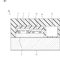
- FIG. 1A and 1B are a front sectional view of an acoustic wave device according to the first embodiment of the present invention and a plan view of the acoustic wave device of the first embodiment except for a sealing resin layer.
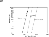
- FIG. FIG. 2 is a diagram showing the relationship between the bump diameter, the number of cycles in the heat shock test, and the failure rate.
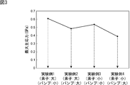
- FIG. 3 is a diagram showing the relationship between the element size and bump size of the acoustic wave elements of Experimental Examples 1 to 4 and the maximum principal stress on the bump upper surface at ⁇ 40 ° C. after mounting.
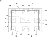
- FIG. 4 is a schematic plan view for explaining the positional relationship between bumps and electrode lands in Experimental Examples 1 to 4 shown in FIG.
- FIG. 5 (a) to 5 (d) are schematic partial cutaway front cross-sectional views for explaining the deformation and fracture mechanism of the metal bump when thermal stress is applied.
- FIG. 6 is a diagram showing the relationship between the sealing width and the maximum principal stress on the upper surface of the Au bump at ⁇ 40 ° C. after mounting.
- FIG. 7 is a schematic front cross-sectional view for explaining a sealing width in a module component.
- FIG. 1A is a front cross-sectional view of an elastic wave device according to a first embodiment of the present invention
- FIG. 1B shows a sealing resin layer in the elastic wave device of the first embodiment. It is a top view removed and shown.
- the acoustic wave device 1 has a package substrate 2.
- the package substrate 2 has first and second main surfaces 2a and 2b facing each other.
- the package substrate 2 is made of alumina.
- the material of the package substrate 2 other insulating ceramics, synthetic resins, or the like may be used. That is, the package substrate may be made of a ceramic substrate or a printed substrate.
- a plurality of electrode lands 3a, 3b, 4a and 4b are provided on the first main surface 2a of the package substrate 2.
- the electrode lands 3a, 3b, 4a, 4b are made of an appropriate metal such as W, Mo, Ag, Cu, or an alloy mainly composed of these.
- the first and second acoustic wave elements 11 and 12 are mounted on the package substrate 2.
- the acoustic wave device 1 is a duplexer having first and second bandpass filters.
- the first acoustic wave element 11 has a first piezoelectric substrate 13.
- the first piezoelectric substrate 13 has first and second main surfaces 13a and 13b facing each other, and side surfaces 13c to 13f connecting the first main surface 13a and the second main surface 13b.
- An IDT electrode 14 is provided on the first main surface 13a.
- FIG. 1A only the IDT electrode 14 is illustrated, but a plurality of IDT electrodes are provided on the first main surface 13a in order to form a plurality of acoustic wave resonators. Thereby, the first band-pass filter is configured.
- Terminal electrodes 15a and 15b are provided on the first main surface 13a.
- the terminal electrodes 15a and 15b are joined to the electrode lands 3a and 3b by first Au bumps 16a and 16b as metal bumps.
- first Au bumps 16a and 16b as metal bumps.
- FIG. 1B on the first main surface 13a of the first piezoelectric substrate 13, six first Au bumps 16a to 16f are arranged. That is, the first acoustic wave element 11 is mounted on the package substrate 2 using the first Au bumps 16a to 16f in a face-down manner.
- the plane area of the second acoustic wave element 12 when viewed in plan is smaller than that of the first acoustic wave element 11.
- the second acoustic wave element 12 has a second piezoelectric substrate 23.
- the second piezoelectric substrate 23 has first and second main surfaces 23a and 23b facing each other. Further, as shown in FIG. 1B, the second piezoelectric substrate 23 has side surfaces 23c to 23f.
- the IDT electrode 24 is provided on the first main surface 23 a of the second piezoelectric substrate 23. Also in the second acoustic wave element 12, a plurality of IDT electrodes are provided on the first main surface 23 a of the second piezoelectric substrate 23. Thereby, the second band-pass filter is configured.
- the pass bands of the first band pass filter and the second band pass filter are the first pass band and the second pass band, respectively.
- the first pass band is located on the lower frequency side than the second pass band. Therefore, the electrode finger pitch of the IDT electrode 14 is larger than the electrode finger pitch of the IDT electrode 24.
- the elastic wave element located on the low frequency side is larger in size. Therefore, in this embodiment, the plane area of the second piezoelectric substrate 23 is smaller than the plane area of the first piezoelectric substrate 13.
- Terminal electrodes 25 a and 25 b are provided on the first main surface 23 a of the second piezoelectric substrate 23.
- the terminal electrodes 25a and 25b are joined to the electrode lands 4a and 4b by second Au bumps 26a and 26b as metal bumps.
- second Au bumps 26a and 26b are provided on the lower surface of the second piezoelectric substrate 23.
- the second acoustic wave element 12 is also mounted on the package substrate 2 in a face-down manner.
- the first and second piezoelectric substrates 13 and 23 are made of a piezoelectric single crystal or a piezoelectric ceramic such as LiTaO 3 or LiNbO 3 .
- the IDT electrodes 14 and 24 and the terminal electrodes 15a, 15b, 25a, and 25b are made of an appropriate metal such as Al, Cu, Ag, or an alloy mainly composed of these.
- a sealing resin layer 5 is provided so as to cover the first and second acoustic wave elements 11 and 12.
- the sealing resin layer 5 is made of an appropriate synthetic resin such as an epoxy resin.
- the sealing resin layer 5 does not reach the area surrounded by the plurality of first Au bumps 16a to 16f and the area surrounded by the plurality of second Au bumps 26a to 26f. This is to form the hollow spaces A and B.
- the feature of the acoustic wave device 1 is that the first Au bumps 16a to 16f as the first metal bumps are larger than the second Au bumps 26a to 26f as the second metal bumps. That is, in the relatively large first elastic wave element 11, the first Au bumps 16a to 16f used are the second metal bumps used in the relatively small second elastic wave element 12. Larger than the second Au bumps 26a to 26f. As a result, even if a thermal shock is applied during reflow, heat shock testing, or actual use, the first Au bumps 16a to 16f and the second Au bumps 26a to 26f are unlikely to peel off due to thermal stress. This will be described with reference to FIGS.
- the size of the first Au bumps 16a to 16f and the second Au bumps 26a to 26f is the same as that of the first Au bumps 16a to 16f when seen in plan view and the second Au bumps 26a to 26f. It is determined by the plane area of the Au bumps 26a to 26f. Therefore, the size of the Au bumps may be determined by the size of the diameters of the Au bumps 16a to 16f and 26a to 26f proportional to the plane area.
- the inventors of the present application have used the relatively large first Au bumps 16a to 16f on the first elastic wave element 11 side having a relatively large size. For example, it has been found that the peeling of the first Au bumps 16a to 16f can be effectively suppressed.
- FIG. 2 is a diagram showing the relationship between the diameter of the Au bump, the number of cycles in the heat shock (HS) test, and the failure rate Ft (%).
- HS heat shock
- Ft failure rate
- the failure rate increases as the number of heat shock test cycles increases. It can be seen that the heat shock resistance increases as the diameter of the Au bump increases from 100 ⁇ m to 120 ⁇ m and 150 ⁇ m.
- the failure rate Ft (%) is the ratio of the acoustic wave device in which the filter characteristics are reduced after the heat shock test and the filter characteristics are worse than before the test.
- the first and second acoustic wave elements 11 and 12 were mounted on the package substrate 2 at a temperature of 250 ° C. according to the flip chip bonding method. Thereafter, the maximum principal stress on the upper surface of the Au bump on the second acoustic wave element 12 side when cooled to ⁇ 40 ° C. and maintained for 30 minutes was measured by a stress analysis simulation. In this case, the following Experimental Examples 1 to 4 were performed.
- Experimental example 2 Size of second elastic wave element 12: large. Specifically, the second piezoelectric substrate 23 having a size of 0.85 mm ⁇ 1.32 mm ⁇ 0.2 mm was used. The size of the second Au bumps 26a to 26f: large. Specifically, the diameters of the second Au bumps 26a to 26f were 150 ⁇ m.
- Experimental example 4 Size of second elastic wave element 12: small. Specifically, the second piezoelectric substrate 23 having a size of 0.81 mm ⁇ 1.11 mm ⁇ 0.2 mm was used. The size of the second Au bumps 26a to 26f: large. Specifically, the diameters of the second Au bumps 26a to 26f were 150 ⁇ m.
- FIG. 4 is a schematic plan view showing the positional relationship between the second Au bumps 26a to 26f joining the second acoustic wave element 12 in Experimental Example 1 and the electrode land.
- FIG. 3 is a diagram showing the relationship between the element size and bump size of the acoustic wave elements of Experimental Examples 1 to 4 and the maximum principal stress on the bump upper surface at ⁇ 40 ° C. after mounting.
- the vertical axis represents the maximum principal stress on the upper surface of the second Au bump 26e.
- the maximum principal stress applied to the second Au bump 26e varies greatly depending on the size of the plane area of the second acoustic wave element 12 and the size of the second Au bump 26e. Recognize. In FIG. 3, only the maximum principal stress on the second Au bump 26e is shown, but it has been confirmed that the same tendency exists in the other second Au bumps 26a to 26d and 26f.
- the first Au bumps 16a to 16f on the first acoustic wave element 11 side to which a larger thermal stress is applied are made larger than the second Au bumps 26a to 26f. This makes it difficult for the first Au bumps 16a to 16f and the second Au bumps 26a to 26f to peel off when heat shock is applied.
- the second Au bumps 26a to 26f are relatively small. Therefore, downsizing can be promoted.
- FIG. 5 (a) shows the initial state, which is under a temperature of about 25 ° C.
- the Au bump 101 joins the terminal electrode 102 of the acoustic wave element 104 and the electrode land 103 on the package substrate 106.
- the temperature is first maintained at 125 ° C. for 30 minutes.
- the upper portion of the Au bump 101 is the X direction that is the outer direction of the package. Try to move to.
- the thermal stress can be reduced by providing relatively large first Au bumps 16a to 16f on the side of the first acoustic wave element 11 having a large plane area. Therefore, the first Au bumps 16a to 16f are hardly peeled off. In addition, the second Au bumps 26a to 26f are not easily subjected to a large thermal stress, and thus are unlikely to peel off.
- the second sealing by the sealing resin layer 5 in the second acoustic wave element 12 described below is performed. It is desirable to make the width W2 larger than the first sealing width W1 by the sealing resin layer 5 of the first acoustic wave element 11.
- the first and second sealing widths W1 and W2 are the side surfaces 13c to 13f and 23c to 23c of the first and second piezoelectric substrates 13 and 23 of the first and second acoustic wave elements 11 and 12, respectively.
- the sealing width W1 in the first acoustic wave element 11 is shown in FIGS. 1 (a) and 1 (b).
- the second sealing width W2 of the second acoustic wave element 12 is also shown in FIGS. 1 (a) and 1 (b). That is, the first sealing width W1 is defined between the side surface 13d of the first piezoelectric substrate 13 closest to the first Au bump 16a and the outer side surface 5a of the sealing resin layer 5 facing the side surface 13d. Is the distance between.
- the second sealing width W2 is between the side surface 23f of the second piezoelectric substrate 23 closest to the second Au bump 26b and the outer surface 5b of the sealing resin layer 5 facing the side surface 23f. Is the distance.
- FIG. 6 is a diagram showing the relationship between the sealing width and the maximum principal stress applied to the upper surface of the Au bump.
- This maximum principal stress is a stress applied to the upper surface of the second Au bump after being maintained at ⁇ 40 ° C. for 30 minutes after mounting the package substrate.
- the monitor in FIG. 6 is a sealing resin layer having a size of 2.1 mm ⁇ 1.6 mm ⁇ 0.4 mm, the size of the second acoustic wave element 12 is a planar shape of 0.75 mm ⁇ 1.32 mm, the first This is the result when the planar shape of the elastic wave element 11 is 0.85 mm ⁇ 1.32 mm and the sealing width of the second elastic wave element 12 is 150 ⁇ m. As is apparent from FIG.
- the thermal stress increases when the sealing width is narrowed by 50 ⁇ m or 100 ⁇ m than the sealing width of the monitor. Therefore, it is desirable to increase the second sealing width on the relatively small second acoustic wave element 12 side, where the influence of the sealing width is relatively large. Therefore, it is preferable that the second sealing width W2 is wider than the first sealing width W1 on the second acoustic wave element 12 side where the change in thermal stress greatly affects.
- the sealing width means the outer surface of the sealing resin layer covering the first and second acoustic wave elements themselves and the first and second acoustic wave elements. It is defined by the distance between the side surfaces of the second piezoelectric substrate. Therefore, for example, in the module component 31 as in the modification shown in FIG. 7, the resin layer 34 located on the outermost side of the module component 31 may not be considered. In the module component 31 shown in FIG. 7, not only the acoustic wave device 1 of the above embodiment but also other electronic components 33 are mounted on the module substrate 32. The elastic wave device 1 and the electronic component 33 are covered with a resin layer 34. The resin layer 34 does not correspond to a sealing resin layer that directly covers the first and second acoustic wave elements 11 and 12. Also in the module component 31, the sealing width may be defined on the basis of the outermost surface of the sealing resin layer 5.
- the first and second Au bumps 16a to 16f and 26a to 26f are used as the first and second metal bumps.
- solder bumps may be used.
- the HS test was performed when the bump diameter was 80 ⁇ m and when the bump diameter was 100 ⁇ m. That is, the number of times of failure was measured by setting the above-mentioned step of maintaining at ⁇ 40 ° C. for 30 minutes and the step of maintaining at 125 ° C. for 30 minutes as one cycle. The results are shown in Table 1 below.
- the elastic wave apparatus which concerns on this invention is widely applied to the various elastic wave apparatuses with which the several elastic wave element is mounted in the package board
- a semiconductor element that is electrically connected to at least one of the first and second acoustic wave elements may be provided.
- the semiconductor element may be mounted on the package substrate.
- the material for the substrate of the acoustic wave device or the semiconductor device is not particularly limited.
- a piezoelectric single crystal such as LiTaO 3 or LiNbO 3 or a piezoelectric material such as piezoelectric ceramics, or a semiconductor such as Si or GaAs can be given.
- SYMBOLS 1 Elastic wave apparatus 2 ... Package board
Landscapes
- Physics & Mathematics (AREA)
- Acoustics & Sound (AREA)
- Surface Acoustic Wave Elements And Circuit Networks Thereof (AREA)
Abstract
Description

2…パッケージ基板
2a,2b…第1,第2の主面
3a,3b,4a,4b…電極ランド
5…封止樹脂層
5a…外側面
5b…外表面
11,12…第1,第2の弾性波素子
13…圧電基板
13a,13b…第1,第2の主面
13c~13f…側面
14…IDT電極
15a,15b…端子電極
16a~16f…第1のAuバンプ
23…圧電基板
23a,23b…第1,第2の主面
23c~23f…側面
24…IDT電極
25a,25b…端子電極
26a~26f…第2のAuバンプ
31…モジュール部品
32…モジュール基板
33…電子部品
34…樹脂層
101…Auバンプ
102…端子電極
103…電極ランド
104…弾性波素子
105…圧電基板
106…パッケージ基板
W1,W2…封止幅
Claims (8)
- パッケージ基板と、
前記パッケージ基板上に第1の金属バンプを介して実装されている第1の弾性波素子と、
前記パッケージ基板上に第2の金属バンプを介して実装されており、前記第1の弾性波素子よりも、平面視した場合の平面積が小さい第2の弾性波素子と、
前記第1の弾性波素子及び前記第2の弾性波素子を覆うように設けられた封止樹脂層と、
を備え、
前記第1の金属バンプが、前記第2の金属バンプよりも大きい、弾性波装置。 - 前記パッケージ基板は、セラミック基板またはプリント基板からなる、請求項1に記載の弾性波装置。
- 平面視した場合の平面積が、前記第1の金属バンプよりも前記第2の金属バンプの方が小さい、請求項1または請求項2に記載の弾性波装置。
- 前記第1及び第2の金属バンプは、それぞれ複数存在し、
前記第1及び第2の弾性波素子において、前記複数の第1の金属バンプで囲まれた領域及び前記複数の第2の金属バンプで囲まれた領域には、前記封止樹脂層が至っていない、請求項1~3のいずれか1項に記載の弾性波装置。 - 前記第1の弾性波素子は、一対の主面と主面同士を結ぶ側面を有する第1の圧電基板と、前記第1の圧電基板上に設けられた第1のIDT電極とを有し、
前記第2の弾性波素子は、一対の主面と主面同士を結ぶ側面を有する第2の圧電基板と、前記第2の圧電基板上に設けられた第2のIDT電極とを有し、
前記第1の弾性波素子において、前記封止樹脂層の外側面と、該外側面と対向している前記第1の圧電基板の前記側面であって前記第1の金属バンプに最も近い前記側面との間の距離のうち最も小さい距離を第1の封止幅とし、
前記第2の弾性波素子において、前記封止樹脂層の外側面と、該外側面と対向している前記第2の圧電基板の側面であって、前記第2の金属バンプに最も近い前記側面との間の距離のうち最も小さい距離を第2の封止幅としたとき、前記第2の封止幅が、前記第1の封止幅よりも広い、請求項1~4のいずれか1項に記載の弾性波装置。 - 前記金属バンプが、Auバンプまたは半田バンプである、請求項1~5のいずれか1項に記載の弾性波装置。
- 前記第1の弾性波素子が、第1の帯域通過型フィルタであり、
前記第2の弾性波素子が、第2の帯域通過型フィルタであり、
前記第1の帯域通過型フィルタの通過帯域が、前記第2の帯域通過型フィルタの通過帯域よりも低周波数側に位置している、請求項1~6のいずれか1項に記載の弾性波装置。 - 前記第1の弾性波素子及び前記第2の弾性波素子の少なくとも一方に電気的に接続されている半導体素子をさらに備える、請求項1~5のいずれか1項に記載の弾性波装置。
Priority Applications (2)
| Application Number | Priority Date | Filing Date | Title |
|---|---|---|---|
| KR1020187010125A KR102091424B1 (ko) | 2015-12-21 | 2016-10-04 | 탄성파 장치 |
| CN201680062237.XA CN108352822B (zh) | 2015-12-21 | 2016-10-04 | 弹性波装置 |
Applications Claiming Priority (2)
| Application Number | Priority Date | Filing Date | Title |
|---|---|---|---|
| JP2015248691 | 2015-12-21 | ||
| JP2015-248691 | 2015-12-21 |
Publications (1)
| Publication Number | Publication Date |
|---|---|
| WO2017110198A1 true WO2017110198A1 (ja) | 2017-06-29 |
Family
ID=59089249
Family Applications (1)
| Application Number | Title | Priority Date | Filing Date |
|---|---|---|---|
| PCT/JP2016/079478 Ceased WO2017110198A1 (ja) | 2015-12-21 | 2016-10-04 | 弾性波装置 |
Country Status (3)
| Country | Link |
|---|---|
| KR (1) | KR102091424B1 (ja) |
| CN (1) | CN108352822B (ja) |
| WO (1) | WO2017110198A1 (ja) |
Cited By (2)
| Publication number | Priority date | Publication date | Assignee | Title |
|---|---|---|---|---|
| CN114785312A (zh) * | 2021-01-22 | 2022-07-22 | 三安日本科技株式会社 | 弹性波装置封装 |
| WO2022255082A1 (ja) * | 2021-06-01 | 2022-12-08 | 株式会社村田製作所 | 弾性波装置 |
Families Citing this family (1)
| Publication number | Priority date | Publication date | Assignee | Title |
|---|---|---|---|---|
| JP2022138735A (ja) * | 2021-03-10 | 2022-09-26 | 三安ジャパンテクノロジー株式会社 | 弾性波デバイス、その弾性波デバイスを備えるモジュール、およびその弾性波デバイスの製造方法 |
Citations (3)
| Publication number | Priority date | Publication date | Assignee | Title |
|---|---|---|---|---|
| JP2004007372A (ja) * | 2002-04-09 | 2004-01-08 | Murata Mfg Co Ltd | 弾性表面波装置の製造方法およびこれを用いた弾性表面波装置、並びに通信装置 |
| JP2006074749A (ja) * | 2004-08-04 | 2006-03-16 | Matsushita Electric Ind Co Ltd | アンテナ共用器、ならびに、それを用いた高周波モジュールおよび通信機器 |
| WO2011077773A1 (ja) * | 2009-12-25 | 2011-06-30 | 株式会社村田製作所 | 分波器 |
Family Cites Families (6)
| Publication number | Priority date | Publication date | Assignee | Title |
|---|---|---|---|---|
| JP2005129610A (ja) * | 2003-10-22 | 2005-05-19 | Tdk Corp | 電子部品 |
| US7446629B2 (en) * | 2004-08-04 | 2008-11-04 | Matsushita Electric Industrial Co., Ltd. | Antenna duplexer, and RF module and communication apparatus using the same |
| CN2773906Y (zh) * | 2004-12-30 | 2006-04-19 | 威宇科技测试封装有限公司 | 一种覆晶芯片堆叠封装结构 |
| JP2012054309A (ja) * | 2010-08-31 | 2012-03-15 | Fujikura Ltd | 半導体装置および電子機器 |
| KR101176349B1 (ko) * | 2010-10-05 | 2012-08-24 | 앰코 테크놀로지 코리아 주식회사 | 칩 적층형 반도체 장치 및 그 제조 방법 |
| KR20150066184A (ko) * | 2013-12-06 | 2015-06-16 | 삼성전자주식회사 | 반도체 패키지 및 그 제조방법 |
-
2016
- 2016-10-04 WO PCT/JP2016/079478 patent/WO2017110198A1/ja not_active Ceased
- 2016-10-04 KR KR1020187010125A patent/KR102091424B1/ko active Active
- 2016-10-04 CN CN201680062237.XA patent/CN108352822B/zh active Active
Patent Citations (3)
| Publication number | Priority date | Publication date | Assignee | Title |
|---|---|---|---|---|
| JP2004007372A (ja) * | 2002-04-09 | 2004-01-08 | Murata Mfg Co Ltd | 弾性表面波装置の製造方法およびこれを用いた弾性表面波装置、並びに通信装置 |
| JP2006074749A (ja) * | 2004-08-04 | 2006-03-16 | Matsushita Electric Ind Co Ltd | アンテナ共用器、ならびに、それを用いた高周波モジュールおよび通信機器 |
| WO2011077773A1 (ja) * | 2009-12-25 | 2011-06-30 | 株式会社村田製作所 | 分波器 |
Cited By (3)
| Publication number | Priority date | Publication date | Assignee | Title |
|---|---|---|---|---|
| CN114785312A (zh) * | 2021-01-22 | 2022-07-22 | 三安日本科技株式会社 | 弹性波装置封装 |
| WO2022255082A1 (ja) * | 2021-06-01 | 2022-12-08 | 株式会社村田製作所 | 弾性波装置 |
| US12431859B2 (en) | 2021-06-01 | 2025-09-30 | Murata Manufacturing Co., Ltd. | Acoustic wave device |
Also Published As
| Publication number | Publication date |
|---|---|
| KR102091424B1 (ko) | 2020-03-20 |
| KR20180050737A (ko) | 2018-05-15 |
| CN108352822B (zh) | 2021-12-07 |
| CN108352822A (zh) | 2018-07-31 |
Similar Documents
| Publication | Publication Date | Title |
|---|---|---|
| US10250222B2 (en) | Electronic device | |
| JP4460612B2 (ja) | 弾性表面波デバイス及びその製造方法 | |
| JP6397352B2 (ja) | 弾性波デバイス | |
| EP2246979A1 (en) | Elastic wave device and method for manufacturing the same | |
| JP7117828B2 (ja) | 弾性波デバイス | |
| JP6315650B2 (ja) | 電子デバイス | |
| CN107615660A (zh) | 弹性波滤波器装置 | |
| CN107210727B (zh) | 电子部件 | |
| US10586778B2 (en) | Elastic wave element and elastic wave apparatus | |
| JP2013131711A (ja) | 電子部品 | |
| JP6407102B2 (ja) | 弾性波デバイス及びその製造方法 | |
| US20180102759A1 (en) | Elastic wave device | |
| JP2015015546A (ja) | 高周波モジュール | |
| JP6433930B2 (ja) | 弾性波デバイス | |
| US20180062611A1 (en) | Rf module including saw device, method of manufacturing the rf module, the saw device, and method of manufacturing the saw device | |
| WO2017110198A1 (ja) | 弾性波装置 | |
| CN104168004A (zh) | 电子元件及其制造方法 | |
| US9941461B2 (en) | Electronic component element and composite module including the same | |
| JP2019054067A (ja) | 電子部品 | |
| US7550902B2 (en) | Electronic component device | |
| US9621127B2 (en) | Elastic wave device with a bump defining a shield and manufacturing method thereof | |
| JP6431191B2 (ja) | 配線基板、電子装置および電子モジュール | |
| CN114793100A (zh) | 弹性波装置及模块 | |
| US11817846B2 (en) | Electronic component | |
| JP6793009B2 (ja) | 弾性波デバイス及び多面取り基板 |
Legal Events
| Date | Code | Title | Description |
|---|---|---|---|
| 121 | Ep: the epo has been informed by wipo that ep was designated in this application |
Ref document number: 16878096 Country of ref document: EP Kind code of ref document: A1 |
|
| ENP | Entry into the national phase |
Ref document number: 20187010125 Country of ref document: KR Kind code of ref document: A |
|
| NENP | Non-entry into the national phase |
Ref country code: DE |
|
| 122 | Ep: pct application non-entry in european phase |
Ref document number: 16878096 Country of ref document: EP Kind code of ref document: A1 |
|
| NENP | Non-entry into the national phase |
Ref country code: JP |