KR20180050737A - 탄성파 장치 - Google Patents
탄성파 장치 Download PDFInfo
- Publication number
- KR20180050737A KR20180050737A KR1020187010125A KR20187010125A KR20180050737A KR 20180050737 A KR20180050737 A KR 20180050737A KR 1020187010125 A KR1020187010125 A KR 1020187010125A KR 20187010125 A KR20187010125 A KR 20187010125A KR 20180050737 A KR20180050737 A KR 20180050737A
- Authority
- KR
- South Korea
- Prior art keywords
- acoustic wave
- bumps
- wave element
- wave device
- bump
- Prior art date
- Legal status (The legal status is an assumption and is not a legal conclusion. Google has not performed a legal analysis and makes no representation as to the accuracy of the status listed.)
- Granted
Links
Images


Classifications
-
- H—ELECTRICITY
- H03—ELECTRONIC CIRCUITRY
- H03H—IMPEDANCE NETWORKS, e.g. RESONANT CIRCUITS; RESONATORS
- H03H9/00—Networks comprising electromechanical or electro-acoustic elements; Electromechanical resonators
- H03H9/25—Constructional features of resonators using surface acoustic waves
-
- H01L21/67121—
-
- H01L24/10—
-
- H—ELECTRICITY
- H03—ELECTRONIC CIRCUITRY
- H03H—IMPEDANCE NETWORKS, e.g. RESONANT CIRCUITS; RESONATORS
- H03H9/00—Networks comprising electromechanical or electro-acoustic elements; Electromechanical resonators
- H03H9/70—Multiple-port networks for connecting several sources or loads, working on different frequencies or frequency bands, to a common load or source
- H03H9/72—Networks using surface acoustic waves
-
- H—ELECTRICITY
- H10—SEMICONDUCTOR DEVICES; ELECTRIC SOLID-STATE DEVICES NOT OTHERWISE PROVIDED FOR
- H10P—GENERIC PROCESSES OR APPARATUS FOR THE MANUFACTURE OR TREATMENT OF DEVICES COVERED BY CLASS H10
- H10P72/00—Handling or holding of wafers, substrates or devices during manufacture or treatment thereof
- H10P72/04—Apparatus for manufacture or treatment
- H10P72/0438—Apparatus for making assemblies not otherwise provided for, e.g. package constructions
-
- H—ELECTRICITY
- H10—SEMICONDUCTOR DEVICES; ELECTRIC SOLID-STATE DEVICES NOT OTHERWISE PROVIDED FOR
- H10W—GENERIC PACKAGES, INTERCONNECTIONS, CONNECTORS OR OTHER CONSTRUCTIONAL DETAILS OF DEVICES COVERED BY CLASS H10
- H10W72/00—Interconnections or connectors in packages
- H10W72/20—Bump connectors, e.g. solder bumps or copper pillars; Dummy bumps; Thermal bumps
Landscapes
- Physics & Mathematics (AREA)
- Acoustics & Sound (AREA)
- Surface Acoustic Wave Elements And Circuit Networks Thereof (AREA)
Abstract
Description
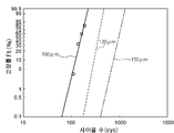
도 2는, 범프의 지름과, 히트 쇼크 시험에 있어서의 사이클 수와, 고장률의 관계를 나타내는 도면이다.
도 3은, 실험예 1~4의 탄성파 소자에 있어서의 소자의 크기와 범프의 크기와, 실장 후 -40℃에서의 범프 상면의 최대 주응력의 관계를 나타내는 도면이다.
도 4는, 도 3에 나타낸 실험예 1~4에 있어서의 범프와 전극 랜드의 위치 관계를 설명하기 위한 모식적 평면도이다.
도 5(a)~도 5(d)는, 열응력이 가해졌을 때의 금속 범프의 변형 및 파단(破斷) 메커니즘을 설명하기 위한 모식적 부분 절결 정면단면도이다.
도 6은, 밀봉 폭과, 실장 후 -40℃에서의 Au 범프 상면의 최대 주응력의 관계를 나타내는 도면이다.
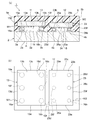
도 7은, 모듈 부품에 있어서의 밀봉 폭을 설명하기 위한 모식적 정면단면도이다.
| HS 시험(-40~125℃) | ||||||||
| 46사이클 | 106사이클 | 150사이클 | 200사이클 | 250사이클 | 300사이클 | 400사이클 | ||
| 솔더 범프 지름(㎛) |
80 | 0/27 | 0/26 | 0/25 | 5/24 | 10/19 | 3/9 | |
| 100 | 0/28 | 0/27 | 0/26 | 0/25 | 0/24 | 2/22 | 2/20 | |
2a, 2b: 제1, 제2의 주면 3a, 3b, 4a, 4b: 전극 랜드
5: 밀봉 수지층 5a: 외측면
5b: 외표면 11, 12: 제1, 제2의 탄성파 소자
13: 압전 기판 13a, 13b: 제1, 제2의 주면
13c~13f: 측면 14: IDT 전극
15a, 15b: 단자 전극 16a~16f: 제1의 Au 범프
23: 압전 기판 23a, 23b: 제1, 제2의 주면
23c~23f: 측면 24: IDT 전극
25a, 25b: 단자 전극 26a~26f: 제2의 Au 범프
31: 모듈 부품 32: 모듈 기판
33: 전자부품 34: 수지층
101: Au 범프 102: 단자 전극
103: 전극 랜드 104: 탄성파 소자
105: 압전 기판 106: 패키지 기판
W1, W2: 밀봉 폭
Claims (8)
- 패키지 기판과,
상기 패키지 기판 상에 제1의 금속 범프를 통해 실장되어 있는 제1의 탄성파 소자와,
상기 패키지 기판 상에 제2의 금속 범프를 통해 실장되어 있으며, 상기 제1의 탄성파 소자보다도 평면에서 본 경우의 평면적이 작은 제2의 탄성파 소자와,
상기 제1의 탄성파 소자 및 상기 제2의 탄성파 소자를 덮도록 마련된 밀봉 수지층을 포함하고,
상기 제1의 금속 범프가 상기 제2의 금속 범프보다도 큰 것을 특징으로 하는 탄성파 장치. - 제1항에 있어서,
상기 패키지 기판은 세라믹 기판 또는 프린트 기판으로 이루어지는 것을 특징으로 하는 탄성파 장치. - 제1항 또는 제2항에 있어서,
평면에서 본 경우의 평면적이 상기 제1의 금속 범프보다도 상기 제2의 금속 범프 쪽이 작은 것을 특징으로 하는 탄성파 장치. - 제1항 내지 제3항 중 어느 한 항에 있어서,
상기 제1 및 제2의 금속 범프는 각각 복수개 존재하고,
상기 제1 및 제2의 탄성파 소자에 있어서, 상기 복수개의 제1의 금속 범프로 둘러싸인 영역 및 상기 복수개의 제2의 금속 범프로 둘러싸인 영역에는, 상기 밀봉 수지층이 이르지 않은 것을 특징으로 하는 탄성파 장치. - 제1항 내지 제4항 중 어느 한 항에 있어서,
상기 제1의 탄성파 소자는, 한 쌍의 주면(主面)과 주면끼리를 잇는 측면을 가지는 제1의 압전 기판과, 상기 제1의 압전 기판 상에 마련된 제1의 IDT 전극을 가지고,
상기 제2의 탄성파 소자는, 한 쌍의 주면과 주면끼리를 잇는 측면을 가지는 제2의 압전 기판과, 상기 제2의 압전 기판 상에 마련된 제2의 IDT 전극을 가지며,
상기 제1의 탄성파 소자에 있어서, 상기 밀봉 수지층의 외측면과, 상기 외측면과 대향하고 있는 상기 제1의 압전 기판의 상기 측면으로서 상기 제1의 금속 범프에 가장 가까운 상기 측면 사이의 거리 중 가장 작은 거리를 제1의 밀봉 폭으로 하고,
상기 제2의 탄성파 소자에 있어서, 상기 밀봉 수지층의 외측면과, 상기 외측면과 대향하고 있는 상기 제2의 압전 기판의 측면으로서 상기 제2의 금속 범프에 가장 가까운 상기 측면 사이의 거리 중 가장 작은 거리를 제2의 밀봉 폭으로 했을 때, 상기 제2의 밀봉 폭이 상기 제1의 밀봉 폭보다도 넓은 것을 특징으로 하는 탄성파 장치. - 제1항 내지 제5항 중 어느 한 항에 있어서,
상기 금속 범프가, Au 범프 또는 솔더 범프인 것을 특징으로 하는 탄성파 장치. - 제1항 내지 제6항 중 어느 한 항에 있어서,
상기 제1의 탄성파 소자가 제1의 대역통과형 필터이고,
상기 제2의 탄성파 소자가 제2의 대역통과형 필터이며,
상기 제1의 대역통과형 필터의 통과 대역이 상기 제2의 대역통과형 필터의 통과 대역보다도 저 주파수 측에 위치하고 있는 것을 특징으로 하는 탄성파 장치. - 제1항 내지 제5항 중 어느 한 항에 있어서,
상기 제1의 탄성파 소자 및 상기 제2의 탄성파 소자의 적어도 한 쪽에 전기적으로 접속되어 있는 반도체소자를 더 포함하는 것을 특징으로 하는 탄성파 장치.
Applications Claiming Priority (3)
| Application Number | Priority Date | Filing Date | Title |
|---|---|---|---|
| JP2015248691 | 2015-12-21 | ||
| JPJP-P-2015-248691 | 2015-12-21 | ||
| PCT/JP2016/079478 WO2017110198A1 (ja) | 2015-12-21 | 2016-10-04 | 弾性波装置 |
Publications (2)
| Publication Number | Publication Date |
|---|---|
| KR20180050737A true KR20180050737A (ko) | 2018-05-15 |
| KR102091424B1 KR102091424B1 (ko) | 2020-03-20 |
Family
ID=59089249
Family Applications (1)
| Application Number | Title | Priority Date | Filing Date |
|---|---|---|---|
| KR1020187010125A Active KR102091424B1 (ko) | 2015-12-21 | 2016-10-04 | 탄성파 장치 |
Country Status (3)
| Country | Link |
|---|---|
| KR (1) | KR102091424B1 (ko) |
| CN (1) | CN108352822B (ko) |
| WO (1) | WO2017110198A1 (ko) |
Families Citing this family (3)
| Publication number | Priority date | Publication date | Assignee | Title |
|---|---|---|---|---|
| JP7610248B2 (ja) * | 2021-01-22 | 2025-01-08 | 三安ジャパンテクノロジー株式会社 | 弾性波デバイスパッケージ |
| JP2022138735A (ja) * | 2021-03-10 | 2022-09-26 | 三安ジャパンテクノロジー株式会社 | 弾性波デバイス、その弾性波デバイスを備えるモジュール、およびその弾性波デバイスの製造方法 |
| WO2022255082A1 (ja) | 2021-06-01 | 2022-12-08 | 株式会社村田製作所 | 弾性波装置 |
Citations (5)
| Publication number | Priority date | Publication date | Assignee | Title |
|---|---|---|---|---|
| JP2004007372A (ja) | 2002-04-09 | 2004-01-08 | Murata Mfg Co Ltd | 弾性表面波装置の製造方法およびこれを用いた弾性表面波装置、並びに通信装置 |
| JP2006074749A (ja) * | 2004-08-04 | 2006-03-16 | Matsushita Electric Ind Co Ltd | アンテナ共用器、ならびに、それを用いた高周波モジュールおよび通信機器 |
| JP2012054309A (ja) * | 2010-08-31 | 2012-03-15 | Fujikura Ltd | 半導体装置および電子機器 |
| KR20120035248A (ko) * | 2010-10-05 | 2012-04-16 | 앰코 테크놀로지 코리아 주식회사 | 칩 적층형 반도체 장치 및 그 제조 방법 |
| JP5170262B2 (ja) * | 2009-12-25 | 2013-03-27 | 株式会社村田製作所 | 分波器 |
Family Cites Families (4)
| Publication number | Priority date | Publication date | Assignee | Title |
|---|---|---|---|---|
| JP2005129610A (ja) * | 2003-10-22 | 2005-05-19 | Tdk Corp | 電子部品 |
| US7446629B2 (en) * | 2004-08-04 | 2008-11-04 | Matsushita Electric Industrial Co., Ltd. | Antenna duplexer, and RF module and communication apparatus using the same |
| CN2773906Y (zh) * | 2004-12-30 | 2006-04-19 | 威宇科技测试封装有限公司 | 一种覆晶芯片堆叠封装结构 |
| KR20150066184A (ko) * | 2013-12-06 | 2015-06-16 | 삼성전자주식회사 | 반도체 패키지 및 그 제조방법 |
-
2016
- 2016-10-04 WO PCT/JP2016/079478 patent/WO2017110198A1/ja not_active Ceased
- 2016-10-04 KR KR1020187010125A patent/KR102091424B1/ko active Active
- 2016-10-04 CN CN201680062237.XA patent/CN108352822B/zh active Active
Patent Citations (5)
| Publication number | Priority date | Publication date | Assignee | Title |
|---|---|---|---|---|
| JP2004007372A (ja) | 2002-04-09 | 2004-01-08 | Murata Mfg Co Ltd | 弾性表面波装置の製造方法およびこれを用いた弾性表面波装置、並びに通信装置 |
| JP2006074749A (ja) * | 2004-08-04 | 2006-03-16 | Matsushita Electric Ind Co Ltd | アンテナ共用器、ならびに、それを用いた高周波モジュールおよび通信機器 |
| JP5170262B2 (ja) * | 2009-12-25 | 2013-03-27 | 株式会社村田製作所 | 分波器 |
| JP2012054309A (ja) * | 2010-08-31 | 2012-03-15 | Fujikura Ltd | 半導体装置および電子機器 |
| KR20120035248A (ko) * | 2010-10-05 | 2012-04-16 | 앰코 테크놀로지 코리아 주식회사 | 칩 적층형 반도체 장치 및 그 제조 방법 |
Also Published As
| Publication number | Publication date |
|---|---|
| KR102091424B1 (ko) | 2020-03-20 |
| CN108352822B (zh) | 2021-12-07 |
| WO2017110198A1 (ja) | 2017-06-29 |
| CN108352822A (zh) | 2018-07-31 |
Similar Documents
| Publication | Publication Date | Title |
|---|---|---|
| KR100691160B1 (ko) | 적층형 표면탄성파 패키지 및 그 제조방법 | |
| US8279610B2 (en) | Electronic component package, base of electronic component package, and junction structure of electronic component package and circuit substrate | |
| JP6397352B2 (ja) | 弾性波デバイス | |
| JP6315650B2 (ja) | 電子デバイス | |
| US10586778B2 (en) | Elastic wave element and elastic wave apparatus | |
| WO2019216300A1 (ja) | 高周波モジュール | |
| KR102091424B1 (ko) | 탄성파 장치 | |
| US10580750B2 (en) | Electronic component | |
| JP2020145596A (ja) | 弾性波デバイス、フィルタおよびマルチプレクサ | |
| US7550902B2 (en) | Electronic component device | |
| EP3086364B1 (en) | Electronic component-use package and piezoelectric device | |
| US9306538B2 (en) | Composite electronic component | |
| US11817846B2 (en) | Electronic component | |
| JP6793009B2 (ja) | 弾性波デバイス及び多面取り基板 | |
| JP6253306B2 (ja) | 電子デバイス | |
| JP4234088B2 (ja) | 電子部品及びその製造方法 | |
| JP5268335B2 (ja) | 圧電部品 | |
| WO2018198508A1 (ja) | 弾性波装置、および、それを用いた高周波フロントエンド回路、通信装置 | |
| JP2016181759A (ja) | 電子デバイス | |
| JP7281146B2 (ja) | 弾性波デバイス | |
| WO2016152905A1 (ja) | 配線基板、電子装置および電子モジュール | |
| CN105321905A (zh) | 焊接结构和包括焊接结构的电子组件模块 | |
| KR20190138104A (ko) | 표면탄성파 소자 패키지 및 그 제작 방법 | |
| JP2005136079A (ja) | 半導体装置及びその実装構造 |
Legal Events
| Date | Code | Title | Description |
|---|---|---|---|
| A201 | Request for examination | ||
| P11-X000 | Amendment of application requested |
St.27 status event code: A-2-2-P10-P11-nap-X000 |
|
| P13-X000 | Application amended |
St.27 status event code: A-2-2-P10-P13-nap-X000 |
|
| PA0105 | International application |
St.27 status event code: A-0-1-A10-A15-nap-PA0105 |
|
| PA0201 | Request for examination |
St.27 status event code: A-1-2-D10-D11-exm-PA0201 |
|
| PG1501 | Laying open of application |
St.27 status event code: A-1-1-Q10-Q12-nap-PG1501 |
|
| D13-X000 | Search requested |
St.27 status event code: A-1-2-D10-D13-srh-X000 |
|
| D14-X000 | Search report completed |
St.27 status event code: A-1-2-D10-D14-srh-X000 |
|
| E902 | Notification of reason for refusal | ||
| PE0902 | Notice of grounds for rejection |
St.27 status event code: A-1-2-D10-D21-exm-PE0902 |
|
| E13-X000 | Pre-grant limitation requested |
St.27 status event code: A-2-3-E10-E13-lim-X000 |
|
| P11-X000 | Amendment of application requested |
St.27 status event code: A-2-2-P10-P11-nap-X000 |
|
| P13-X000 | Application amended |
St.27 status event code: A-2-2-P10-P13-nap-X000 |
|
| E701 | Decision to grant or registration of patent right | ||
| PE0701 | Decision of registration |
St.27 status event code: A-1-2-D10-D22-exm-PE0701 |
|
| GRNT | Written decision to grant | ||
| PR0701 | Registration of establishment |
St.27 status event code: A-2-4-F10-F11-exm-PR0701 |
|
| PR1002 | Payment of registration fee |
St.27 status event code: A-2-2-U10-U12-oth-PR1002 Fee payment year number: 1 |
|
| PG1601 | Publication of registration |
St.27 status event code: A-4-4-Q10-Q13-nap-PG1601 |
|
| PR1001 | Payment of annual fee |
St.27 status event code: A-4-4-U10-U11-oth-PR1001 Fee payment year number: 4 |
|
| PR1001 | Payment of annual fee |
St.27 status event code: A-4-4-U10-U11-oth-PR1001 Fee payment year number: 5 |
|
| PR1001 | Payment of annual fee |
St.27 status event code: A-4-4-U10-U11-oth-PR1001 Fee payment year number: 6 |
|
| P22-X000 | Classification modified |
St.27 status event code: A-4-4-P10-P22-nap-X000 |