KR20180050737A - Seismic wave device - Google Patents
Seismic wave device Download PDFInfo
- Publication number
- KR20180050737A KR20180050737A KR1020187010125A KR20187010125A KR20180050737A KR 20180050737 A KR20180050737 A KR 20180050737A KR 1020187010125 A KR1020187010125 A KR 1020187010125A KR 20187010125 A KR20187010125 A KR 20187010125A KR 20180050737 A KR20180050737 A KR 20180050737A
- Authority
- KR
- South Korea
- Prior art keywords
- acoustic wave
- bumps
- wave element
- wave device
- bump
- Prior art date
- Legal status (The legal status is an assumption and is not a legal conclusion. Google has not performed a legal analysis and makes no representation as to the accuracy of the status listed.)
- Granted
Links
Images


Classifications
-
- H—ELECTRICITY
- H03—ELECTRONIC CIRCUITRY
- H03H—IMPEDANCE NETWORKS, e.g. RESONANT CIRCUITS; RESONATORS
- H03H9/00—Networks comprising electromechanical or electro-acoustic elements; Electromechanical resonators
- H03H9/25—Constructional features of resonators using surface acoustic waves
-
- H01L21/67121—
-
- H01L24/10—
-
- H—ELECTRICITY
- H03—ELECTRONIC CIRCUITRY
- H03H—IMPEDANCE NETWORKS, e.g. RESONANT CIRCUITS; RESONATORS
- H03H9/00—Networks comprising electromechanical or electro-acoustic elements; Electromechanical resonators
- H03H9/70—Multiple-port networks for connecting several sources or loads, working on different frequencies or frequency bands, to a common load or source
- H03H9/72—Networks using surface acoustic waves
-
- H—ELECTRICITY
- H10—SEMICONDUCTOR DEVICES; ELECTRIC SOLID-STATE DEVICES NOT OTHERWISE PROVIDED FOR
- H10P—GENERIC PROCESSES OR APPARATUS FOR THE MANUFACTURE OR TREATMENT OF DEVICES COVERED BY CLASS H10
- H10P72/00—Handling or holding of wafers, substrates or devices during manufacture or treatment thereof
- H10P72/04—Apparatus for manufacture or treatment
- H10P72/0438—Apparatus for making assemblies not otherwise provided for, e.g. package constructions
-
- H—ELECTRICITY
- H10—SEMICONDUCTOR DEVICES; ELECTRIC SOLID-STATE DEVICES NOT OTHERWISE PROVIDED FOR
- H10W—GENERIC PACKAGES, INTERCONNECTIONS, CONNECTORS OR OTHER CONSTRUCTIONAL DETAILS OF DEVICES COVERED BY CLASS H10
- H10W72/00—Interconnections or connectors in packages
- H10W72/20—Bump connectors, e.g. solder bumps or copper pillars; Dummy bumps; Thermal bumps
Landscapes
- Physics & Mathematics (AREA)
- Acoustics & Sound (AREA)
- Surface Acoustic Wave Elements And Circuit Networks Thereof (AREA)
Abstract
열이 가해진 경우라도 평면적이 상대적으로 큰 탄성파 소자의 금속 범프의 박리가 생기기 어려운 탄성파 장치를 제공한다. 패키지 기판(2) 상에 평면에서 본 경우의 평면적이 큰 제1의 탄성파 소자(11)와, 평면에서 본 경우의 평면적이 작은 제2의 탄성파 소자(12)가, 각각 제1의 금속 범프(16a~16f) 및 제2의 금속 범프(26a~26f)를 통해 실장되어 있고, 밀봉 수지층(5)이 제1의 탄성파 소자(11)및 제2의 탄성파 소자(12)를 덮도록 마련되어 있고, 제1의 금속 범프(16a~16f)가 제2의 금속 범프(26a~26f)보다도 커져 있는 탄성파 장치(1).There is provided a seismic wave device in which separation of metal bumps of an acoustic wave device having a relatively large planarity is difficult to occur even when heat is applied. The first acoustic wave element 11 having a large planar surface in a plan view and the second acoustic wave element 12 having a small planar surface in a plan view on the package substrate 2 are bonded to the first metal bump 16a to 16f and second metal bumps 26a to 26f and the sealing resin layer 5 is provided so as to cover the first acoustic wave element 11 and the second acoustic wave element 12 , And the first metal bumps (16a - 16f) are larger than the second metal bumps (26a - 26f).
Description
본 발명은, 패키지 기판 상에 복수개의 탄성파 소자가 탑재되어 있는 탄성파 장치에 관한 것이다. The present invention relates to an elastic wave device in which a plurality of elastic wave devices are mounted on a package substrate.
종래, 복수개의 탄성파 소자가 패키지 기판 상에 탑재되어 있는 탄성파 장치가 여러 가지 알려져 있다. 예를 들면, 하기의 특허문헌 1에 기재된 탄성파 장치에서는, 평면에서 본 경우의 평면적이 상대적으로 큰 탄성파 소자와, 평면적이 상대적으로 작은 탄성파 소자가 동일한 사이즈의 금속 범프를 이용해서 패키지 기판 상에 탑재되어 있다. BACKGROUND ART [0002] Conventionally, various elastic wave devices in which a plurality of elastic wave devices are mounted on a package substrate are known. For example, in the acoustic wave device described in
금속 범프의 사이즈가 탄성파 소자에 비해 작으면, 열응력에 의한 일그러진 영향을 받기 쉬워진다. 그 때문에, 평면적이 상대적으로 큰 탄성파 소자의 금속 범프에 큰 열응력이 걸리게 되어, 평면적이 상대적으로 큰 탄성파 소자의 금속 범프가 박리될 우려가 있었다. If the size of the metal bump is smaller than that of the acoustic wave element, it is easily affected by the thermal stress. Therefore, a large thermal stress is applied to the metal bumps of the acoustic wave element having a relatively large planar surface, and there is a fear that the metal bumps of the acoustic wave element having a relatively large planar surface are peeled off.
본 발명의 목적은, 열이 가해진 경우라도 평면적이 상대적으로 큰 탄성파 소자의 금속 범프가 박리되기 어려운 탄성파 장치를 제공하는 것에 있다. It is an object of the present invention to provide an elastic wave device in which metal bumps of an elastic wave device having a relatively large planar surface are difficult to peel off even when heat is applied.
본 발명에 따르는 탄성파 장치는, 패키지 기판과, 상기 패키지 기판 상에 제1의 금속 범프를 통해 실장되어 있는 제1의 탄성파 소자와, 상기 패키지 기판 상에 제2의 금속 범프를 통해 실장되어 있으며, 상기 제1의 탄성파 소자보다도 평면에서 본 경우의 평면적이 작은 제2의 탄성파 소자와, 상기 제1의 탄성파 소자 및 상기 제2의 탄성파 소자를 덮도록 마련된 밀봉 수지층을 포함하고, 상기 제1의 금속 범프가 상기 제2의 금속 범프보다도 크다. An acoustic wave device according to the present invention includes a package substrate, a first acoustic wave element mounted on the package substrate through a first metal bump, and a second acoustic wave element mounted on the package substrate via a second metal bump, A second acoustic wave element having a smaller planar area in a plane view than the first acoustic wave element and a sealing resin layer provided so as to cover the first acoustic wave element and the second acoustic wave element, The metal bumps are larger than the second metal bumps.
본 발명에 따르는 탄성파 장치의 어떤 특정한 국면에서는, 상기 패키지 기판은 세라믹 기판 또는 프린트 기판으로 이루어진다. In a specific aspect of the acoustic wave device according to the present invention, the package substrate is composed of a ceramic substrate or a printed substrate.
본 발명에 따르는 탄성파 장치의 다른 특정한 국면에서는, 평면에서 본 경우의 평면적이 상기 제1의 금속 범프보다도 상기 제2의 금속 범프 쪽이 작다. In another specific aspect of the acoustic wave device according to the present invention, the plane view of the acoustic wave device is smaller than the first metal bump and the second metal bump.
본 발명에 따르는 탄성파 장치의 별도의 특정한 국면에서는, 상기 제1 및 제2의 금속 범프는 각각 복수개 존재하고, 상기 제1 및 제2의 탄성파 소자에 있어서 상기 복수개의 제1의 금속 범프로 둘러싸인 영역 및 상기 복수개의 제2의 금속 범프로 둘러싸인 영역에는 상기 밀봉 수지층이 이르지 않고 있다.In another specific aspect of the acoustic wave device according to the present invention, a plurality of the first and second metal bumps are present, and in the first and second acoustic wave devices, a region surrounded by the plurality of first metal bumps And the sealing resin layer does not reach the region surrounded by the plurality of second metal bumps.
본 발명에 따르는 탄성파 장치의 또 다른 특정한 국면에서는, 상기 제1의 탄성파 소자는 한 쌍의 주면(主面)과 주면끼리를 잇는 측면을 가지는 제1의 압전 기판과, 상기 제1의 압전 기판 상에 마련된 제1의 IDT 전극을 가지고, 상기 제2의 탄성파 소자는 한 쌍의 주면과 주면끼리를 잇는 측면을 가지는 제2의 압전 기판과, 상기 제2의 압전 기판 상에 마련된 제2의 IDT 전극을 가지며, 상기 제1의 탄성파 소자에 있어서, 상기 밀봉 수지층의 외측면과, 상기 외측면과 대향하고 있는 상기 제1의 압전 기판의 상기 측면으로서 상기 제1의 금속 범프에 가장 가까운 상기 측면 사이의 거리 중 가장 작은 거리를 제1의 밀봉 폭으로 하고, 상기 제2의 탄성파 소자에 있어서, 상기 밀봉 수지층의 외측면과, 상기 외측면과 대향하고 있는 상기 제2의 압전 기판의 측면으로서 상기 제2의 금속 범프에 가장 가까운 상기 측면 사이의 거리 중 가장 작은 거리를 제2의 밀봉 폭으로 했을 때, 상기 제2의 밀봉 폭이 상기 제1의 밀봉 폭보다도 넓다. 이 경우에는, 열에 의한 범프의 박리가 보다 한층 생기기 어렵다. In another specific aspect of the acoustic wave device according to the present invention, the first acoustic wave device includes a first piezoelectric substrate having a pair of main surfaces and side surfaces connecting the main surfaces, Wherein the second acoustic wave device has a second piezoelectric substrate having a pair of main surfaces and side surfaces connecting the main surfaces, and a second IDT electrode provided on the second piezoelectric substrate, Wherein the first acoustic wave element has an outer side surface of the sealing resin layer and a side surface of the first piezoelectric substrate facing the outer side surface and between the side surface closest to the first metal bump as the side surface of the first piezoelectric substrate Of the first piezoelectric substrate is set to a first sealing width, and in the second acoustic wave device, an outer surface of the sealing resin layer and an upper surface of the second piezoelectric substrate facing the outer surface, When the smallest distance of the distance between the second closest to the side of the metal bump with a sealing width of the second, the sealing width of the second larger than the sealing width of the first. In this case, peeling of the bumps due to heat is more difficult to occur.
본 발명에 따르는 탄성파 장치의 또 다른 특정한 국면에서는, 상기 금속 범프가 Au 범프 또는 솔더 범프이다. In another specific aspect of the acoustic wave device according to the present invention, the metal bumps are Au bumps or solder bumps.
본 발명에 따르는 탄성파 장치의 다른 특정한 국면에서는, 상기 제1의 탄성파 소자가 제1의 대역통과형 필터이고, 상기 제2의 탄성파 소자가 제2의 대역통과형 필터이며, 상기 제1의 대역통과형 필터의 통과 대역이 상기 제2의 대역통과형 필터의 통과 대역보다도 저 주파수 측에 위치하고 있다. In another specific aspect of the acoustic wave device according to the present invention, the first acoustic wave device is a first band-pass filter, the second acoustic wave device is a second band-pass filter, Type filter is located on a lower frequency side than the pass band of the second band-pass filter.
본 발명에 따르는 탄성파 장치의 또 다른 특정한 국면에서는, 상기 제1의 탄성파 소자 및 상기 제2의 탄성파 소자의 적어도 한 쪽에 전기적으로 접속되어 있는 반도체소자를 더 포함한다.In another specific aspect of the acoustic wave device according to the present invention, the semiconductor device further includes a semiconductor element electrically connected to at least one of the first acoustic wave element and the second acoustic wave element.
본 발명에 따르는 탄성파 장치에 의하면, 평면적이 큰 탄성파 소자와, 평면적이 작은 탄성파 소자를 패키지 기판 상에 탑재했다고 해도, 평면적이 상대적으로 큰 탄성파 소자에 있어서, 금속 범프의 박리가 생기기 어렵다. According to the acoustic wave device according to the present invention, even when the acoustic wave device having a large planar surface and the acoustic wave device having a small planar surface are mounted on a package substrate, peeling of the metal bump is unlikely to occur in an acoustic wave device having a relatively large planar surface.
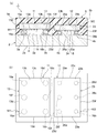
도 1(a) 및 도 1(b)는, 본 발명의 제1의 실시형태에 따르는 탄성파 장치의 정면단면도 및 밀봉 수지층을 제외하고 나타내는 제1의 실시형태의 탄성파 장치의 평면도이다.
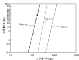
도 2는, 범프의 지름과, 히트 쇼크 시험에 있어서의 사이클 수와, 고장률의 관계를 나타내는 도면이다.
도 3은, 실험예 1~4의 탄성파 소자에 있어서의 소자의 크기와 범프의 크기와, 실장 후 -40℃에서의 범프 상면의 최대 주응력의 관계를 나타내는 도면이다.
도 4는, 도 3에 나타낸 실험예 1~4에 있어서의 범프와 전극 랜드의 위치 관계를 설명하기 위한 모식적 평면도이다.
도 5(a)~도 5(d)는, 열응력이 가해졌을 때의 금속 범프의 변형 및 파단(破斷) 메커니즘을 설명하기 위한 모식적 부분 절결 정면단면도이다.
도 6은, 밀봉 폭과, 실장 후 -40℃에서의 Au 범프 상면의 최대 주응력의 관계를 나타내는 도면이다.
도 7은, 모듈 부품에 있어서의 밀봉 폭을 설명하기 위한 모식적 정면단면도이다. 1 (a) and 1 (b) are a front cross-sectional view of an acoustic wave device according to a first embodiment of the present invention and a plan view of the acoustic wave device of the first embodiment except for the sealing resin layer.
2 is a diagram showing the relationship between the diameter of the bump, the number of cycles in the heat shock test, and the failure rate.
Fig. 3 is a diagram showing the relationship between the element size and bump size in the acoustic wave devices of Experimental Examples 1 to 4 and the maximum principal stress of the bump upper surface at -40 deg. C after mounting. Fig.
4 is a schematic plan view for explaining the positional relationship between bumps and electrode lands in Experimental Examples 1 to 4 shown in Fig. 3; Fig.
5 (a) to 5 (d) are schematic partial cutaway front sectional views for explaining a deformation and fracture mechanism of a metal bump when thermal stress is applied.
6 is a diagram showing the relationship between the sealing width and the maximum principal stress at the upper surface of the Au bump at -40 ° C after mounting.
7 is a schematic front sectional view for explaining a sealing width in a module part.
이하, 도면을 참조하면서 본 발명의 구체적인 실시형태를 설명함으로써 본 발명을 분명히 한다. DETAILED DESCRIPTION OF THE PREFERRED EMBODIMENTS Hereinafter, the present invention will be made clear by describing specific embodiments of the present invention with reference to the drawings.
또한, 본 명세서에 기재된 각 실시형태는 예시적인 것이며, 다른 실시형태 사이에서 구성의 부분적인 치환 또는 조합이 가능한 것을 지적해 둔다. Furthermore, it is pointed out that each embodiment described in this specification is illustrative, and partial substitution or combination of constitution is possible between different embodiments.
도 1(a)는 본 발명의 제1의 실시형태에 따르는 탄성파 장치의 정면단면도이고, 도 1(b)는 제1의 실시형태의 탄성파 장치에서 밀봉 수지층을 제거해서 나타내는 평면도이다. Fig. 1 (a) is a front sectional view of an acoustic wave device according to a first embodiment of the present invention, and Fig. 1 (b) is a plan view showing a state in which a sealing resin layer is removed from the acoustic wave device of the first embodiment.
탄성파 장치(1)는 패키지 기판(2)을 가진다. 패키지 기판(2)은, 서로 대향하는 제1, 제2의 주면(2a, 2b)을 가진다. 패키지 기판(2)은, 본 실시형태에서는 알루미나로 이루어진다. 단, 패키지 기판(2)의 재료로서는, 다른 절연성 세라믹스나, 합성 수지 등을 이용해도 된다. 즉, 패키지 기판은, 세라믹 기판 또는 프린트 기판 등으로 이루어져 있어도 된다. The elastic wave device (1) has a package substrate (2). The
패키지 기판(2)의 제1의 주면(2a) 상에, 복수개의 전극 랜드(3a, 3b, 4a, 4b)가 마련되어 있다. 전극 랜드(3a, 3b, 4a, 4b)는, W, Mo, Ag, Cu 또는 이들을 주재료로 하는 합금 등의 적당한 금속으로 이루어진다. A plurality of
패키지 기판(2) 상에는 제1, 제2의 탄성파 소자(11, 12)가 실장되어 있다. 탄성파 장치(1)는 제1 및 제2의 대역통과형 필터를 가지는 듀플렉서이다. On the
제1의 탄성파 소자(11)는, 제1의 압전 기판(13)을 가진다. 제1의 압전 기판(13)은, 서로 대향하는 제1 및 제2의 주면(13a, 13b)과, 제1의 주면(13a)과 제2의 주면(13b)을 잇고 있는 측면(13c~13f)을 가진다. 제1의 주면 (13a) 상에 IDT 전극(14)이 마련되어 있다. 도 1(a)에서는, IDT 전극(14)만을 도시하고 있지만, 제1의 주면(13a) 상에는 복수개의 탄성파 공진자를 구성하기 위해 복수개의 IDT 전극이 마련되어 있다. 그것에 의해 제1의 대역통과형 필터가 구성되어 있다. The first
제1의 주면(13a) 상에는 단자 전극(15a, 15b)이 마련되어 있다. 단자 전극(15a, 15b)이 금속 범프로서의 제1의 Au 범프(16a, 16b)에 의해 전극 랜드(3a, 3b)에 접합되어 있다. 도 1(b)에 나타내는 바와 같이, 상기 제1의 압전 기판(13)의 제1의 주면(13a) 상에는, 6개의 제1의 Au 범프(16a~16f)가 배치되어 있다. 즉, 제1의 탄성파 소자(11)는 페이스 다운 방식으로 제1의 Au 범프(16a~16f)를 이용해서 패키지 기판(2)에 실장되어 있다.
제2의 탄성파 소자(12)는, 제1의 탄성파 소자(11)보다도, 평면에서 봤을 때의 평면적이 작다. 제2의 탄성파 소자(12)는 제2의 압전 기판(23)을 가진다. 제2의 압전 기판(23)은 서로 대향하는 제1, 제2의 주면(23a, 23b)을 가진다. 또한, 도 1(b)에 나타내는 바와 같이, 제2의 압전 기판(23)은 측면(23c~23f)을 가진다. The second
제2의 압전 기판(23)의 제1의 주면(23a) 상에 IDT 전극(24)이 마련되어 있다. 제2의 탄성파 소자(12)에 있어서도, 제2의 압전 기판(23)의 제1의 주면(23a) 상에 복수개의 IDT 전극이 마련되어 있다. 그것에 의해 제2의 대역통과형 필터가 구성되어 있다. The
상기 제1의 대역통과형 필터 및 제2의 대역통과형 필터의 통과 대역을, 각각 제1의 통과 대역 및 제2의 통과 대역으로 한다. 제1의 통과 대역은, 제2의 통과 대역보다도 저 주파수 측에 위치하고 있다. 따라서, IDT 전극(14)의 전극핑거 피치는, IDT 전극(24)의 전극핑거 피치보다 크다. 또한, 일반적으로, 저 주파수 측에 위치하는 탄성파 소자 쪽이 사이즈가 커진다. 따라서, 본 실시형태에서는, 제2의 압전 기판(23)의 평면적이, 제1의 압전 기판(13)의 평면적보다도 작아져 있다. The pass band of the first band pass filter and the pass band of the second band pass filter are respectively set as a first pass band and a second pass band. The first pass band is located on the lower frequency side than the second pass band. Therefore, the electrode finger pitch of the
제2의 압전 기판(23)의 제1의 주면(23a) 상에는, 단자 전극(25a, 25b)이 마련되어 있다. 단자 전극(25a, 25b)은, 금속 범프로서의 제2의 Au 범프(26a, 26b)에 의해, 전극 랜드(4a, 4b)에 접합되어 있다. 실제로는, 도 1(b)에 나타내는 바와 같이, 제2의 압전 기판(23)의 하면에는, 6개의 제2의 Au 범프(26a~26f)가 마련되어 있다. On the first
제2의 탄성파 소자(12)도 또한, 제1의 탄성파 소자(11)와 마찬가지로 페이스 다운 방식으로 패키지 기판(2) 상에 실장되어 있다. The second
상기 제1, 제2의 압전 기판(13, 23)은, LiTaO3이나 LiNbO3 등의 압전 단결정 또는 압전 세라믹스로 이루어진다. 또한, IDT 전극(14, 24) 및 단자 전극(15a, 15b, 25a, 25b)은 Al, Cu, Ag 또는 이들을 주재료로 하는 합금 등의 적당한 금속으로 이루어진다. The first and second
도 1(a)에 나타내는 바와 같이, 제1, 제2의 탄성파 소자(11, 12)를 덮도록 밀봉 수지층(5)이 마련되어 있다. 밀봉 수지층(5)은, 에폭시 수지 등의 적당한 합성 수지로 이루어진다. 밀봉 수지층(5)은, 복수개의 제1의 Au 범프(16a~16f)로 둘러싸여 있는 영역, 및 복수개의 제2의 Au 범프(26a~26f)로 둘러싸여 있는 영역 내에는 이르지 않고 있다. 이것은, 중공 공간(A 및 B)을 형성하기 위해서이다. As shown in Fig. 1 (a), a sealing
탄성파 장치(1)의 특징은, 제1의 금속 범프로서의 제1의 Au 범프(16a~16f)가, 제2의 금속 범프로서의 제2의 Au 범프(26a~26f)보다도 큰 것에 있다. 즉, 상대적으로 큰 제1의 탄성파 소자(11)에 있어서, 이용되고 있는 제1의 Au 범프(16a~16f)가, 상대적으로 작은 제2의 탄성파 소자(12)에 이용되고 있는 제2의 금속 범프로서의 제2의 Au 범프(26a~26f)보다도 크다. 그것에 의해, 리플로우 시, 히트 쇼크 시험 시 혹은 실제 사용 시에 열충격이 가해졌다고 해도, 열응력에 의한 제1의 Au 범프(16a~16f) 및 제2의 Au 범프(26a~26f)의 박리가 생기기 어렵다. 이것을 도 2~도 5를 참조해서 설명하기로 한다.The
또한, 제1의 Au 범프(16a~16f) 및 제2의 Au 범프(26a~26f)의 대소(大小)는, 접합되어 있는 상태에서 평면에서 본 경우의 제1의 Au 범프(16a~16f)의 평면적 및 제2의 Au 범프(26a~26f)의 평면적에 따라 결정된다. 따라서, 상기 평면적에 비례하는 Au 범프(16a~16f, 26a~26f)의 지름의 대소에 따라 Au 범프의 대소를 결정하면 된다. The first Au bumps 16a to 16f and the second Au bumps 26a to 26f are larger in size than the first Au bumps 16a to 16f when viewed in a plan view, And the planarity of the second Au bumps 26a to 26f. Therefore, it is only necessary to determine the size of the Au bumps according to the size of the diameter of the Au bumps 16a to 16f, 26a to 26f proportional to the plane.
본원 발명자들은, 상기 열응력에 의한 금속 범프의 박리에 대해 여러 가지 검토한 결과, 상대적으로 치수가 큰 제1의 탄성파 소자(11) 측에 있어서, 상대적으로 큰 제1의 Au 범프(16a~16f)를 이용하면, 제1의 Au 범프(16a~16f)의 박리를 효과적으로 억제할 수 있는 것을 찾아냈다. The inventors of the present invention have made various studies on peeling of metal bumps by the thermal stress. As a result, it has been found that, on the first
Au 범프의 크기와 열응력이 가해진 경우의 영향에 대해 여러가지 검토했다. 도 2는, Au 범프의 지름과, 히트 쇼크(HS) 시험에 있어서의 사이클 수와, 고장률 Ft(%)의 관계를 나타내는 도면이다. 여기서, 히트 쇼크 시험에서는, 공기 중, -60℃에서 30분간 유지하는 공정과, 다음으로, 190℃의 온도에서 30분간 유지하는 공정을 1사이클로 하여, 복수회의 사이클을 실시하였다. 도 2에 있어서, 실선(實線)은 Au 범프의 지름이 100㎛, 파선(破線)은 120㎛, 일점쇄선은 150㎛인 경우의 결과를 나타낸다. The size of the Au bump and the influence of the application of the thermal stress were examined variously. 2 is a diagram showing the relationship between the diameter of Au bumps, the number of cycles in the heat shock (HS) test, and the failure rate Ft (%). Here, in the heat shock test, a cycle of holding in air at -60 占 폚 for 30 minutes and a cycle of holding at a temperature of 190 占 폚 for 30 minutes as one cycle were carried out a plurality of times. In Fig. 2, the solid line indicates the result when the diameter of the Au bump is 100 mu m, the broken line is 120 mu m, and the one-dot chain line is 150 mu m.
도 2로부터 분명하듯이, 히트 쇼크 시험의 사이클 수가 증가하면 고장률이 높아진다. 그리고, Au 범프의 지름이 100㎛로부터 120㎛ 및 150㎛로 커짐에 따라, 내(耐) 히트 쇼크성이 높아지는 것을 알 수 있다. As apparent from Fig. 2, when the number of cycles of the heat shock test increases, the failure rate increases. It can be seen that the resistance to heat shock increases as the diameter of the Au bumps increases from 100 m to 120 m and 150 m.
여기서, 고장률 Ft(%)란, 히트 쇼크 시험 후에 필터 특성을 도모하여, 필터 특성이 시험 전보다도 악화되고 있는 탄성파 장치의 비율이다. Here, the failure rate Ft (%) is the ratio of the elastic wave device in which the filter characteristics are improved after the heat shock test and the filter characteristics are worse than before the test.
다음으로, 상기 실시형태의 탄성파 장치(1)에 있어서, 패키지 기판(2)에 제1 및 제2의 탄성파 소자(11, 12)를 플립칩 본딩법을 따라 250℃의 온도에서 패키지 기판(2)에 실장했다. 그리고 나서, -40℃까지 냉각하고, 30분 유지한 경우의 제2의 탄성파 소자(12) 측에 있어서의 Au 범프 상면의 최대 주응력을 응력 해석 시뮬레이션에 의해 측정했다. 이 경우, 이하의 실험예 1~4를 실시했다. Next, in the
실험예 1: 제2의 탄성파 소자(12)의 치수: 대(大). 구체적으로는, 제2의 압전 기판(23)으로서 0.85㎜×1.32㎜×0.2㎜인 치수의 것을 이용했다. 제2의 Au 범프(26a~26f)의 크기: 소(小). 구체적으로는, 제2의 Au 범프(26a~26f)의 지름을 110㎛로 했다. Experimental Example 1: Dimension of the second acoustic wave element 12: large. More specifically, the second
실험예 2: 제2의 탄성파 소자(12)의 치수: 대. 구체적으로는, 제2의 압전 기판(23)으로서 0.85㎜×1.32㎜×0.2㎜인 치수의 것을 이용했다. 제2의 Au 범프(26a~26f)의 사이즈: 대. 구체적으로는, 제2의 Au 범프(26a~26f)의 지름을 150㎛로 했다. Experimental Example 2: Dimension of the second acoustic wave device 12: More specifically, the second
실험예 3: 제2의 탄성파 소자(12)의 치수: 소. 구체적으로는, 제2의 압전 기판(23)으로서 0.81㎜×1.11㎜×0.2㎜인 치수의 것을 이용했다. 제2의 Au 범프(26a~26f)의 크기: 소. 구체적으로는, 제2의 Au 범프(26a~26f)의 지름을 110㎛로 했다. Experimental Example 3: Dimension of the second acoustic wave device 12: Small. Specifically, the second
실험예 4: 제2의 탄성파 소자(12)의 치수: 소. 구체적으로는, 제2의 압전 기판(23)으로서 0.81㎜×1.11㎜×0.2㎜인 치수의 것을 이용했다. 제2의 Au 범프(26a~26f)의 사이즈: 대. 구체적으로는, 제2의 Au 범프(26a~26f)의 지름을 150㎛로 했다. Experimental Example 4: Dimension of the second acoustic wave device 12: Small. Specifically, the second
도 4는 실험예 1에 있어서의 제2의 탄성파 소자(12)를 접합하고 있는 제2의 Au 범프(26a~26f)와, 전극 랜드의 위치 관계를 나타내는 모식적 평면도이다. 4 is a schematic plan view showing the positional relationship between the second Au bumps 26a to 26f bonding the second
도 4에 나타내는 제2의 Au 범프(26a~26f) 중, Au 범프(26e) 상면의 최대 주응력을 구했다. 도 3은 실험예 1~4의 탄성파 소자에 있어서의 소자의 크기와 범프의 크기와, 실장 후 -40℃에 있어서의 범프 상면의 최대 주응력의 관계를 나타내는 도면이다. 세로축은, 상기 제2의 Au 범프(26e)의 상면의 최대 주응력이다. Among the second Au bumps 26a to 26f shown in Fig. 4, the maximum principal stress on the upper surface of the
도 3으로부터 분명하듯이, 제2의 탄성파 소자(12)의 평면적의 크기와, 제2의 Au 범프(26e)의 크기에 따라 제2의 Au 범프(26e)에 가해지는 최대 주응력이 크게 변화되는 것을 알 수 있다. 도 3에서는, 제2의 Au 범프(26e) 상의 최대 주응력만을 나타냈지만, 다른 제2의 Au 범프(26a~26d, 26f)에서도 동일한 경향이 있는 것이 확인되고 있다. 3, the maximum principal stress applied to the second Au bumps 26e varies greatly depending on the size of the planar size of the second
또한, 도 3에 있어서 실험예 1과 실험예 2의 대비로부터, 소자의 평면적이 동일한 경우, 제2의 Au 범프(26e)를 크게 함으로써 열응력을 작게 할 수 있는 것을 알 수 있다. 또한, 실험예 3과 실험예 4의 대비로부터, 제2의 탄성파 소자의 평면적이 작은 경우에 있어서도 동일한 평면적이면, 제2의 범프를 크게 함으로써 열응력을 작게 할 수 있는 것을 알 수 있다. It is also understood from the comparison of Experimental Example 1 and Experimental Example 2 in FIG. 3 that the thermal stress can be reduced by enlarging the second Au bumps 26e when the planarities of the elements are the same. It can also be seen from the contrast between Experimental Example 3 and Experimental Example 4 that the thermal stress can be reduced by increasing the second bump if the planar area of the second acoustic wave device is also the same.
실험예 1~4로부터 제2의 Au 범프(26a~26f)를 크게 함으로써, 제2의 탄성파 소자(12)에 있어서의 제2의 Au 범프(26a~26f)에 가해지는 열응력을 작게 할 수 있는 것을 알 수 있다. 즉, Au 범프를 이용한 실장구조에서는, Au 범프를 크게 하는 것이 바람직하다. It is possible to reduce the thermal stress applied to the second Au bumps 26a to 26f in the second
그런데, 히트 쇼크가 가해진 경우, 상대적으로 치수가 큰 제1의 탄성파 소자(11)에, 상대적으로 평면적이 작은 제2의 탄성파 소자(12)보다도 큰 열응력이 가해진다. 따라서, 상대적으로 큰 제1의 탄성파 소자(11)에 있어서, 보다 큰 제1의 Au 범프(16a~16f)를 마련하는 것이 바람직하다. 따라서, 본 실시형태에 의하면, 보다 큰 열응력이 가해지는 제1의 탄성파 소자(11) 측의 제1의 Au 범프(16a~16f)가, 상기 제2의 Au 범프(26a~26f)보다도 커져 있다. 그것에 의해, 히트 쇼크가 가해진 경우의 제1의 Au 범프(16a~16f) 및 제2의 Au 범프(26a~26f)의 박리가 생기기 어렵게 되어 있다. However, when the heat shock is applied, a larger thermal stress is applied to the first
또한, 상대적으로 작은 제2의 탄성파 소자(12)에서는, 제2의 Au 범프(26a~26f)가 상대적으로 작아져 있다. 따라서, 소형화를 진행시키는 것도 가능해진다. In the second
상기 HS 시험에 있어서의 Au 범프의 변형 및 파단 메커니즘을 도 5(a)~도 5(d)에 나타낸다. Figs. 5 (a) to 5 (d) show the deformation and breakage mechanism of the Au bump in the HS test.
도 5(a)는, 초기 상태, 25℃ 정도의 온도 하에 있는 상태를 나타낸다. Au 범프(101)는, 탄성파 소자(104)의 단자 전극(102)과, 패키지 기판(106) 상의 전극 랜드(103)를 접합하고 있다. HS 시험에 있어서, 먼저, 125℃에서 30분 유지한다. 이 경우, 도 5(b)에 화살표 X로 나타내는 바와 같이, 압전 기판(105)의 열팽창 계수가 패키지 기판(106)의 열팽창 계수보다 크기 때문에, Au 범프(101)의 상부가 패키지의 외측 방향인 X 방향으로 이동하려고 한다.5 (a) shows a state under an initial state and a temperature of about 25 캜. The
다음으로, -40℃로 냉각한 상태에서는, 도 5(c)에 나타내는 바와 같이 -X방향으로 응력이 가해진다. 즉, 압전 기판(105) 쪽이 패키지 기판(106)보다 선팽창 계수가 크기 때문에, 안쪽을 향해서 크게 변위된다. 그 때문에, 도 5(c)에 나타내는 바와 같은 크랙(C)이 Au 범프(101)와 단자 전극(102)의 사이에 생긴다. 또한, 다시 125℃로 온도를 높이면, 도 5(d)에 화살표 X로 나타내는 바와 같이, 다시 탄성파 소자(104) 측에서 패키지의 외측을 향해서 큰 응력이 생긴다. 이러한 열응력이 반복해서 역방향으로 가해짐으로써 상기 크랙(C)이 커져, 파단에 이르는 것이라 생각된다. 따라서, 상기 HS 시험 시뿐만 아니라, 리플로우값이나 실제 사용 시에 있어서도 열이 가해지면, 열응력이 가해짐으로써 Au 범프(101)가 단자 전극(102)으로부터 박리될 우려가 있었다. Next, in the state of being cooled to -40 占 폚, stress is applied in the -X direction as shown in Fig. 5 (c). That is, since the
이에 대하여, 상기 실시형태에서는, 평면적이 큰 제1의 탄성파 소자(11) 측에 있어서 상대적으로 큰 제1의 Au 범프(16a~16f)를 마련함으로써, 상기 열응력을 작게 할 수 있다. 따라서, 상기 제1의 Au 범프(16a~16f)의 박리가 생기기 어렵다. 또한, 제2의 Au 범프(26a~26f)에는 그리 큰 열응력이 가해지기 어렵기 때문에 박리가 생기기 어렵다. On the other hand, in the above-described embodiment, the thermal stress can be reduced by providing the relatively large first Au bumps 16a to 16f on the side of the first
또한, 상대적으로 작은 제2의 Au 범프(26a~26f)이더라도, 상기 열응력을 완화하기 위해서는, 이하에서 서술하는 제2의 탄성파 소자(12)에 있어서의 밀봉 수지층(5)에 의한 제2의 밀봉 폭(W2)을, 제1의 탄성파 소자(11)의 밀봉 수지층(5)에 의한 제1의 밀봉 폭(W1)보다도 크게 하는 것이 바람직하다. 여기서, 제1, 제2의 밀봉 폭(W1, W2)이란, 제1, 제2의 탄성파 소자(11, 12)의 제1, 제2의 압전 기판(13, 23)의 측면(13c~13f, 23c~23f) 중의 제1의 Au 범프(16a~16f), 제2의 Au 범프(26a~26f)중 어느 하나에 가장 가까운 측면과, 밀봉 수지층(5)의 외측면 사이의 거리 중, 가장 작은 거리를 말하는 것으로 한다. 제1의 탄성파 소자(11)에 있어서의 밀봉 폭(W1)을, 도 1 (a) 및 도 1(b)에 나타낸다. 제2의 탄성파 소자(12)의 제2의 밀봉 폭(W2)도, 도 1 (a) 및 도 1(b)에 나타낸다. 즉, 제1의 밀봉 폭(W1)은, 제1의 Au 범프(16a)에 가장 가까운 제1의 압전 기판(13)의 측면(13d)과, 상기 측면(13d)과 대향하고 있는 밀봉 수지층(5)의 외측면(5a) 사이의 거리이다. 또한, 제2의 밀봉 폭(W2)은, 제2의 Au 범프(26b)에 가장 가까운 제2의 압전 기판(23)의 측면(23f)과, 측면(23f)과 대향하고 있는 밀봉 수지층(5)의 외표면(5b) 사이의 거리이다. Even in the case of relatively small second Au bumps 26a to 26f, in order to alleviate the thermal stress, it is preferable that the sealing
도 6은, 밀봉 폭과 Au 범프의 상면에 가해지는 최대 주응력의 관계를 나타내는 도면이다. 이 최대 주응력은, 패키지 기판 실장 후 -40℃에서 30분 유지한 후의 제2의 Au 범프의 상면에 가해지는 응력이다. 도 6 중의 모니터란, 2.1㎜×1.6㎜×0.4㎜인 치수의 밀봉 수지층, 제2의 탄성파 소자(12)의 치수를 0.75㎜×1.32㎜의 평면 형상, 제1의 탄성파 소자(11)의 평면 형상을 0.85㎜×1.32㎜로 하고, 제2의 탄성파 소자(12)에 있어서의 밀봉 폭을 150㎛로 한 경우의 결과이다. 도 6으로부터 분명하듯이, 상기 모니터의 밀봉 폭보다도, 밀봉 폭을 50㎛ 또는 100㎛만큼 좁히면, 열응력이 커지는 것을 알 수 있다. 따라서, 상대적으로 밀봉 폭의 영향이 커지는, 상대적으로 작은 제2의 탄성파 소자(12) 측에서 제2의 밀봉 폭을 넓게 하는 것이 바람직하다. 따라서, 바람직하게는, 열응력의 변화가 크게 영향을 주는 제2의 탄성파 소자(12) 측에서, 상기 제2의 밀봉 폭(W2)을 제1의 밀봉 폭(W1)보다도 넓게 하는 것이 바람직하다. 6 is a diagram showing the relationship between the sealing width and the maximum principal stress applied to the upper surface of the Au bump. This maximum principal stress is a stress applied to the upper surface of the second Au bump after being held at -40 캜 for 30 minutes after packaging the package substrate. The monitor in Fig. 6 refers to a sealing resin layer having a size of 2.1 mm x 1.6 mm x 0.4 mm, a second
또한, 상기한 바와 같이 밀봉 폭이란, 제1, 제2의 탄성파 소자 자체를 피복하고 있는 밀봉 수지층의 외측면과, 제1, 제2의 탄성파 소자의 제1, 제2의 압전 기판의 측면 사이의 거리로 정의되는 것이다. 따라서, 예를 들면 도 7에 나타내는 변형예와 같은 모듈 부품(31)에서는, 모듈 부품(31)의 최외측에 위치하고 있는 수지층(34)을 고려하지 않아도 된다. 도 7에 나타내는 모듈 부품(31)에서는, 모듈 기판(32) 상에 상기 실시형태의 탄성파 장치(1) 뿐만 아니라, 다른 전자부품(33)도 탑재되어 있다. 그리고, 상기 탄성파 장치(1)와 전자부품(33)은 수지층(34)에 의해 피복되어 있다. 이 수지층(34)은, 제1, 제2의 탄성파 소자(11, 12)를 직접 피복하고 있는 밀봉 수지층에는 해당하지 않는다. 모듈 부품(31)에 있어서도, 상기 밀봉 폭은, 밀봉 수지층(5)의 최외측면을 기준으로 해서 정의되면 된다. As described above, the sealing width is defined by the outer surface of the sealing resin layer covering the first and second acoustic wave elements themselves and the side surface of the first and second piezoelectric substrates of the first and second acoustic wave elements, As shown in FIG. Therefore, for example, in the
또한, 상기 실시형태에서는, 제1, 제2의 금속 범프로서 제1, 제2의 Au 범프(16a~16f, 26a~26f)를 이용했지만, 솔더 범프를 이용해도 된다. Although the first and second Au bumps 16a to 16f and 26a to 26f are used as the first and second metal bumps in the above embodiment, solder bumps may be used.
솔더 범프에 있어서, 범프의 지름을 80㎛로 한 경우와, 100㎛로 한 경우에 있어서, HS 시험을 실시했다. 즉, 상기 -40℃에서 30분 유지하는 공정과, 125℃에서 30분 유지하는 공정을 1사이클로 하여, 고장에 이르는 수를 측정했다. 결과를 하기의 표 1에 나타낸다.In the solder bumps, the HS test was performed when the bump diameter was 80 mu m and when the bump diameter was 100 mu m. That is, the number of failures was measured by setting the cycle of holding at -40 ° C for 30 minutes and holding at 125 ° C for 30 minutes as one cycle. The results are shown in Table 1 below.
지름(㎛)Solder bump
Diameter (㎛)
표 1로부터 분명하듯이, 솔더 범프의 경우에도 범프의 지름이 커지면 고장률이 저하되는 것을 알 수 있다. 따라서, 솔더 범프를 이용한 경우에 있어서도, 상기 제1의 실시형태와 같이, 제1의 탄성파 소자(11) 측에서 범프를 상대적으로 크게 함으로써 솔더 범프의 박리의 억제를 효과적으로 도모할 수 있다. As can be seen from Table 1, in the case of the solder bump, the failure rate decreases as the diameter of the bump increases. Therefore, even in the case of using the solder bump, it is possible to effectively suppress the peeling of the solder bump by increasing the bump relatively on the side of the first
또한, 탄성파 장치(1)에서는 듀플렉서에 적용한 예를 나타냈지만, 본 발명에 따르는 탄성파 장치는, 복수개의 탄성파 소자가 패키지 기판에 탑재되어 있는 다양한 탄성파 장치에 널리 적용할 수 있다. Although the
또한, 본 발명에 따르는 탄성파 장치에서는, 제1 및 제2의 탄성파 소자의 적어도 한쪽에 전기적으로 접속되어 있는 반도체소자가 포함되어 있어도 된다. 이 경우, 반도체소자는, 상기 패키지 기판 상에 탑재되어 있어도 된다. 탄성파 소자나 반도체소자의 기판의 재료로서는, 특별히 한정되지 않는다. 예를 들면, LiTaO3이나 LiNbO3 등의 압전 단결정 혹은 압전 세라믹스와 같은 압전체, 또는, Si 혹은 GaAs와 같은 반도체를 들 수 있다. 혹은, 도 7에 나타낸 모듈 부품(31)과 같이, 모듈 기판(32) 상에 탑재되어 있는 다른 전자부품(33)으로서 상기 반도체소자를 탑재해도 된다. In the acoustic wave device according to the present invention, a semiconductor element electrically connected to at least one of the first and second acoustic wave elements may be included. In this case, the semiconductor element may be mounted on the package substrate. The material of the substrate of the elastic wave element or the semiconductor element is not particularly limited. For example, piezoelectric single crystals such as LiTaO 3 and LiNbO 3 , piezoelectric materials such as piezoelectric ceramics, or semiconductors such as Si or GaAs. Alternatively, the semiconductor element may be mounted as another
1: 탄성파 장치 2: 패키지 기판
2a, 2b: 제1, 제2의 주면 3a, 3b, 4a, 4b: 전극 랜드
5: 밀봉 수지층 5a: 외측면
5b: 외표면 11, 12: 제1, 제2의 탄성파 소자
13: 압전 기판 13a, 13b: 제1, 제2의 주면
13c~13f: 측면 14: IDT 전극
15a, 15b: 단자 전극 16a~16f: 제1의 Au 범프
23: 압전 기판 23a, 23b: 제1, 제2의 주면
23c~23f: 측면 24: IDT 전극
25a, 25b: 단자 전극 26a~26f: 제2의 Au 범프
31: 모듈 부품 32: 모듈 기판
33: 전자부품 34: 수지층
101: Au 범프 102: 단자 전극
103: 전극 랜드 104: 탄성파 소자
105: 압전 기판 106: 패키지 기판
W1, W2: 밀봉 폭 1: elastic wave device 2: package substrate
2a, 2b: first and second
5: sealing
5b:
13:
13c to 13f: side 14: IDT electrode
15a and 15b:
23:
23c to 23f: side surface 24: IDT electrode
25a and 25b:
31: Module part 32: Module substrate
33: Electronic component 34: Resin layer
101: Au bump 102: Terminal electrode
103: electrode land 104: elastic wave element
105: piezoelectric substrate 106: package substrate
W1, W2: Sealing width
Claims (8)
상기 패키지 기판 상에 제1의 금속 범프를 통해 실장되어 있는 제1의 탄성파 소자와,
상기 패키지 기판 상에 제2의 금속 범프를 통해 실장되어 있으며, 상기 제1의 탄성파 소자보다도 평면에서 본 경우의 평면적이 작은 제2의 탄성파 소자와,
상기 제1의 탄성파 소자 및 상기 제2의 탄성파 소자를 덮도록 마련된 밀봉 수지층을 포함하고,
상기 제1의 금속 범프가 상기 제2의 금속 범프보다도 큰 것을 특징으로 하는 탄성파 장치. A package substrate,
A first acoustic wave element mounted on the package substrate through a first metal bump,
A second acoustic wave element mounted on the package substrate through a second metal bump and having a smaller planarity in plan view than the first acoustic wave element,
And a sealing resin layer covering the first acoustic wave element and the second acoustic wave element,
Wherein the first metal bump is larger than the second metal bump.
상기 패키지 기판은 세라믹 기판 또는 프린트 기판으로 이루어지는 것을 특징으로 하는 탄성파 장치. The method according to claim 1,
Wherein the package substrate comprises a ceramic substrate or a printed substrate.
평면에서 본 경우의 평면적이 상기 제1의 금속 범프보다도 상기 제2의 금속 범프 쪽이 작은 것을 특징으로 하는 탄성파 장치. 3. The method according to claim 1 or 2,
Wherein the planar surface of the second metal bump is smaller than the first metal bump.
상기 제1 및 제2의 금속 범프는 각각 복수개 존재하고,
상기 제1 및 제2의 탄성파 소자에 있어서, 상기 복수개의 제1의 금속 범프로 둘러싸인 영역 및 상기 복수개의 제2의 금속 범프로 둘러싸인 영역에는, 상기 밀봉 수지층이 이르지 않은 것을 특징으로 하는 탄성파 장치. 4. The method according to any one of claims 1 to 3,
A plurality of first and second metal bumps are present,
Wherein in the first and second acoustic wave devices, the sealing resin layer is not formed in the region surrounded by the plurality of first metal bumps and in the region surrounded by the plurality of second metal bumps. .
상기 제1의 탄성파 소자는, 한 쌍의 주면(主面)과 주면끼리를 잇는 측면을 가지는 제1의 압전 기판과, 상기 제1의 압전 기판 상에 마련된 제1의 IDT 전극을 가지고,
상기 제2의 탄성파 소자는, 한 쌍의 주면과 주면끼리를 잇는 측면을 가지는 제2의 압전 기판과, 상기 제2의 압전 기판 상에 마련된 제2의 IDT 전극을 가지며,
상기 제1의 탄성파 소자에 있어서, 상기 밀봉 수지층의 외측면과, 상기 외측면과 대향하고 있는 상기 제1의 압전 기판의 상기 측면으로서 상기 제1의 금속 범프에 가장 가까운 상기 측면 사이의 거리 중 가장 작은 거리를 제1의 밀봉 폭으로 하고,
상기 제2의 탄성파 소자에 있어서, 상기 밀봉 수지층의 외측면과, 상기 외측면과 대향하고 있는 상기 제2의 압전 기판의 측면으로서 상기 제2의 금속 범프에 가장 가까운 상기 측면 사이의 거리 중 가장 작은 거리를 제2의 밀봉 폭으로 했을 때, 상기 제2의 밀봉 폭이 상기 제1의 밀봉 폭보다도 넓은 것을 특징으로 하는 탄성파 장치. 5. The method according to any one of claims 1 to 4,
The first acoustic wave device has a first piezoelectric substrate having a pair of main surfaces and a side connecting surfaces of the main surfaces and a first IDT electrode provided on the first piezoelectric substrate,
The second acoustic wave device has a second piezoelectric substrate having a pair of main surfaces and side surfaces connecting the main surfaces and a second IDT electrode provided on the second piezoelectric substrate,
The first acoustic wave element is characterized in that an outer side surface of the sealing resin layer and a side surface of the first piezoelectric substrate facing the outer side surface, The smallest distance is the first sealing width,
The second acoustic wave element is characterized in that an outer side surface of the sealing resin layer and a side surface of the second piezoelectric substrate facing the outer side surface And the second sealing width is larger than the first sealing width when the smallest distance is the second sealing width.
상기 금속 범프가, Au 범프 또는 솔더 범프인 것을 특징으로 하는 탄성파 장치. 6. The method according to any one of claims 1 to 5,
Wherein the metal bump is an Au bump or a solder bump.
상기 제1의 탄성파 소자가 제1의 대역통과형 필터이고,
상기 제2의 탄성파 소자가 제2의 대역통과형 필터이며,
상기 제1의 대역통과형 필터의 통과 대역이 상기 제2의 대역통과형 필터의 통과 대역보다도 저 주파수 측에 위치하고 있는 것을 특징으로 하는 탄성파 장치. 7. The method according to any one of claims 1 to 6,
The first acoustic wave element is a first band-pass filter,
The second acoustic wave device is a second band-pass filter,
And the pass band of the first band-pass filter is located on a lower frequency side than the pass band of the second band-pass filter.
상기 제1의 탄성파 소자 및 상기 제2의 탄성파 소자의 적어도 한 쪽에 전기적으로 접속되어 있는 반도체소자를 더 포함하는 것을 특징으로 하는 탄성파 장치. 6. The method according to any one of claims 1 to 5,
Further comprising a semiconductor element electrically connected to at least one of the first acoustic-wave element and the second acoustic-wave element.
Applications Claiming Priority (3)
| Application Number | Priority Date | Filing Date | Title |
|---|---|---|---|
| JP2015248691 | 2015-12-21 | ||
| JPJP-P-2015-248691 | 2015-12-21 | ||
| PCT/JP2016/079478 WO2017110198A1 (en) | 2015-12-21 | 2016-10-04 | Elastic wave device |
Publications (2)
| Publication Number | Publication Date |
|---|---|
| KR20180050737A true KR20180050737A (en) | 2018-05-15 |
| KR102091424B1 KR102091424B1 (en) | 2020-03-20 |
Family
ID=59089249
Family Applications (1)
| Application Number | Title | Priority Date | Filing Date |
|---|---|---|---|
| KR1020187010125A Active KR102091424B1 (en) | 2015-12-21 | 2016-10-04 | Seismic device |
Country Status (3)
| Country | Link |
|---|---|
| KR (1) | KR102091424B1 (en) |
| CN (1) | CN108352822B (en) |
| WO (1) | WO2017110198A1 (en) |
Families Citing this family (3)
| Publication number | Priority date | Publication date | Assignee | Title |
|---|---|---|---|---|
| JP7610248B2 (en) * | 2021-01-22 | 2025-01-08 | 三安ジャパンテクノロジー株式会社 | Acoustic Wave Device Package |
| JP2022138735A (en) * | 2021-03-10 | 2022-09-26 | 三安ジャパンテクノロジー株式会社 | Acoustic wave device, module including acoustic wave device, and method for manufacturing acoustic wave device |
| WO2022255082A1 (en) | 2021-06-01 | 2022-12-08 | 株式会社村田製作所 | Elastic wave device |
Citations (5)
| Publication number | Priority date | Publication date | Assignee | Title |
|---|---|---|---|---|
| JP2004007372A (en) | 2002-04-09 | 2004-01-08 | Murata Mfg Co Ltd | Method for manufacturing surface acoustic wave device, surface acoustic wave device using the same, and communication device |
| JP2006074749A (en) * | 2004-08-04 | 2006-03-16 | Matsushita Electric Ind Co Ltd | Antenna duplexer, and high-frequency module and communication device using the same |
| JP2012054309A (en) * | 2010-08-31 | 2012-03-15 | Fujikura Ltd | Semiconductor device and electronic apparatus |
| KR20120035248A (en) * | 2010-10-05 | 2012-04-16 | 앰코 테크놀로지 코리아 주식회사 | Chip stack package and method for manufacturing the same |
| JP5170262B2 (en) * | 2009-12-25 | 2013-03-27 | 株式会社村田製作所 | Duplexer |
Family Cites Families (4)
| Publication number | Priority date | Publication date | Assignee | Title |
|---|---|---|---|---|
| JP2005129610A (en) * | 2003-10-22 | 2005-05-19 | Tdk Corp | Electronic components |
| US7446629B2 (en) * | 2004-08-04 | 2008-11-04 | Matsushita Electric Industrial Co., Ltd. | Antenna duplexer, and RF module and communication apparatus using the same |
| CN2773906Y (en) * | 2004-12-30 | 2006-04-19 | 威宇科技测试封装有限公司 | Crystal-coated chip piling and packing structure |
| KR20150066184A (en) * | 2013-12-06 | 2015-06-16 | 삼성전자주식회사 | Semiconductor package and method of manufacturing the same |
-
2016
- 2016-10-04 WO PCT/JP2016/079478 patent/WO2017110198A1/en not_active Ceased
- 2016-10-04 KR KR1020187010125A patent/KR102091424B1/en active Active
- 2016-10-04 CN CN201680062237.XA patent/CN108352822B/en active Active
Patent Citations (5)
| Publication number | Priority date | Publication date | Assignee | Title |
|---|---|---|---|---|
| JP2004007372A (en) | 2002-04-09 | 2004-01-08 | Murata Mfg Co Ltd | Method for manufacturing surface acoustic wave device, surface acoustic wave device using the same, and communication device |
| JP2006074749A (en) * | 2004-08-04 | 2006-03-16 | Matsushita Electric Ind Co Ltd | Antenna duplexer, and high-frequency module and communication device using the same |
| JP5170262B2 (en) * | 2009-12-25 | 2013-03-27 | 株式会社村田製作所 | Duplexer |
| JP2012054309A (en) * | 2010-08-31 | 2012-03-15 | Fujikura Ltd | Semiconductor device and electronic apparatus |
| KR20120035248A (en) * | 2010-10-05 | 2012-04-16 | 앰코 테크놀로지 코리아 주식회사 | Chip stack package and method for manufacturing the same |
Also Published As
| Publication number | Publication date |
|---|---|
| KR102091424B1 (en) | 2020-03-20 |
| CN108352822B (en) | 2021-12-07 |
| WO2017110198A1 (en) | 2017-06-29 |
| CN108352822A (en) | 2018-07-31 |
Similar Documents
| Publication | Publication Date | Title |
|---|---|---|
| KR100691160B1 (en) | Laminated surface acoustic wave package and manufacturing method thereof | |
| US8279610B2 (en) | Electronic component package, base of electronic component package, and junction structure of electronic component package and circuit substrate | |
| JP6397352B2 (en) | Elastic wave device | |
| JP6315650B2 (en) | Electronic devices | |
| US10586778B2 (en) | Elastic wave element and elastic wave apparatus | |
| WO2019216300A1 (en) | High-frequency module | |
| KR102091424B1 (en) | Seismic device | |
| US10580750B2 (en) | Electronic component | |
| JP2020145596A (en) | Acoustic wave device, filter, and multiplexer | |
| US7550902B2 (en) | Electronic component device | |
| EP3086364B1 (en) | Electronic component-use package and piezoelectric device | |
| US9306538B2 (en) | Composite electronic component | |
| US11817846B2 (en) | Electronic component | |
| JP6793009B2 (en) | Elastic wave device and multi-chamfered substrate | |
| JP6253306B2 (en) | Electronic devices | |
| JP4234088B2 (en) | Electronic component and manufacturing method thereof | |
| JP5268335B2 (en) | Piezoelectric parts | |
| WO2018198508A1 (en) | Surface acoustic wave device, high frequency front-end circuit using surface acoustic wave device, and communication device using surface acoustic wave device | |
| JP2016181759A (en) | Electronic devices | |
| JP7281146B2 (en) | elastic wave device | |
| WO2016152905A1 (en) | Wiring board, electronic device and electronic module | |
| CN105321905A (en) | Solder joint structure and electronic component module including the same | |
| KR20190138104A (en) | SAW device package and manufacturing method thereof | |
| JP2005136079A (en) | Semiconductor device and its mounting structure |
Legal Events
| Date | Code | Title | Description |
|---|---|---|---|
| A201 | Request for examination | ||
| P11-X000 | Amendment of application requested |
St.27 status event code: A-2-2-P10-P11-nap-X000 |
|
| P13-X000 | Application amended |
St.27 status event code: A-2-2-P10-P13-nap-X000 |
|
| PA0105 | International application |
St.27 status event code: A-0-1-A10-A15-nap-PA0105 |
|
| PA0201 | Request for examination |
St.27 status event code: A-1-2-D10-D11-exm-PA0201 |
|
| PG1501 | Laying open of application |
St.27 status event code: A-1-1-Q10-Q12-nap-PG1501 |
|
| D13-X000 | Search requested |
St.27 status event code: A-1-2-D10-D13-srh-X000 |
|
| D14-X000 | Search report completed |
St.27 status event code: A-1-2-D10-D14-srh-X000 |
|
| E902 | Notification of reason for refusal | ||
| PE0902 | Notice of grounds for rejection |
St.27 status event code: A-1-2-D10-D21-exm-PE0902 |
|
| E13-X000 | Pre-grant limitation requested |
St.27 status event code: A-2-3-E10-E13-lim-X000 |
|
| P11-X000 | Amendment of application requested |
St.27 status event code: A-2-2-P10-P11-nap-X000 |
|
| P13-X000 | Application amended |
St.27 status event code: A-2-2-P10-P13-nap-X000 |
|
| E701 | Decision to grant or registration of patent right | ||
| PE0701 | Decision of registration |
St.27 status event code: A-1-2-D10-D22-exm-PE0701 |
|
| GRNT | Written decision to grant | ||
| PR0701 | Registration of establishment |
St.27 status event code: A-2-4-F10-F11-exm-PR0701 |
|
| PR1002 | Payment of registration fee |
St.27 status event code: A-2-2-U10-U12-oth-PR1002 Fee payment year number: 1 |
|
| PG1601 | Publication of registration |
St.27 status event code: A-4-4-Q10-Q13-nap-PG1601 |
|
| PR1001 | Payment of annual fee |
St.27 status event code: A-4-4-U10-U11-oth-PR1001 Fee payment year number: 4 |
|
| PR1001 | Payment of annual fee |
St.27 status event code: A-4-4-U10-U11-oth-PR1001 Fee payment year number: 5 |
|
| PR1001 | Payment of annual fee |
St.27 status event code: A-4-4-U10-U11-oth-PR1001 Fee payment year number: 6 |
|
| P22-X000 | Classification modified |
St.27 status event code: A-4-4-P10-P22-nap-X000 |