WO2017104748A1 - 調光フィルム - Google Patents
調光フィルム Download PDFInfo
- Publication number
- WO2017104748A1 WO2017104748A1 PCT/JP2016/087376 JP2016087376W WO2017104748A1 WO 2017104748 A1 WO2017104748 A1 WO 2017104748A1 JP 2016087376 W JP2016087376 W JP 2016087376W WO 2017104748 A1 WO2017104748 A1 WO 2017104748A1
- Authority
- WO
- WIPO (PCT)
- Prior art keywords
- layer
- liquid crystal
- spacer particles
- light control
- insulating layer
- Prior art date
- Legal status (The legal status is an assumption and is not a legal conclusion. Google has not performed a legal analysis and makes no representation as to the accuracy of the status listed.)
- Ceased
Links
Images






Classifications
-
- G—PHYSICS
- G02—OPTICS
- G02F—OPTICAL DEVICES OR ARRANGEMENTS FOR THE CONTROL OF LIGHT BY MODIFICATION OF THE OPTICAL PROPERTIES OF THE MEDIA OF THE ELEMENTS INVOLVED THEREIN; NON-LINEAR OPTICS; FREQUENCY-CHANGING OF LIGHT; OPTICAL LOGIC ELEMENTS; OPTICAL ANALOGUE/DIGITAL CONVERTERS
- G02F1/00—Devices or arrangements for the control of the intensity, colour, phase, polarisation or direction of light arriving from an independent light source, e.g. switching, gating or modulating; Non-linear optics
- G02F1/01—Devices or arrangements for the control of the intensity, colour, phase, polarisation or direction of light arriving from an independent light source, e.g. switching, gating or modulating; Non-linear optics for the control of the intensity, phase, polarisation or colour
- G02F1/13—Devices or arrangements for the control of the intensity, colour, phase, polarisation or direction of light arriving from an independent light source, e.g. switching, gating or modulating; Non-linear optics for the control of the intensity, phase, polarisation or colour based on liquid crystals, e.g. single liquid crystal display cells
-
- G—PHYSICS
- G02—OPTICS
- G02F—OPTICAL DEVICES OR ARRANGEMENTS FOR THE CONTROL OF LIGHT BY MODIFICATION OF THE OPTICAL PROPERTIES OF THE MEDIA OF THE ELEMENTS INVOLVED THEREIN; NON-LINEAR OPTICS; FREQUENCY-CHANGING OF LIGHT; OPTICAL LOGIC ELEMENTS; OPTICAL ANALOGUE/DIGITAL CONVERTERS
- G02F1/00—Devices or arrangements for the control of the intensity, colour, phase, polarisation or direction of light arriving from an independent light source, e.g. switching, gating or modulating; Non-linear optics
- G02F1/01—Devices or arrangements for the control of the intensity, colour, phase, polarisation or direction of light arriving from an independent light source, e.g. switching, gating or modulating; Non-linear optics for the control of the intensity, phase, polarisation or colour
- G02F1/13—Devices or arrangements for the control of the intensity, colour, phase, polarisation or direction of light arriving from an independent light source, e.g. switching, gating or modulating; Non-linear optics for the control of the intensity, phase, polarisation or colour based on liquid crystals, e.g. single liquid crystal display cells
- G02F1/133—Constructional arrangements; Operation of liquid crystal cells; Circuit arrangements
- G02F1/1333—Constructional arrangements; Manufacturing methods
- G02F1/1339—Gaskets; Spacers; Sealing of cells
Definitions
- the present invention relates to a light control film that is attached to a window of a passenger car and controls transmission of extraneous light.
- Patent Documents 1 and 2 various devices related to a light control film that controls the transmission of extraneous light by being attached to a window have been proposed (Patent Documents 1 and 2).
- One such light control film uses liquid crystal.
- the light control film using the liquid crystal is manufactured by sandwiching a liquid crystal material with a transparent film material on which a transparent electrode is manufactured to produce a liquid crystal cell, and sandwiching the liquid crystal cell with a linear polarizing plate.
- the orientation of the liquid crystal is changed by changing the electric field applied to the liquid crystal, thereby blocking or transmitting the extraneous light, and further changing the amount of transmitted light. To control.
- a driving method such as a TN (Twisted Nematic) method, an IPS (In-Place-Switching) method, or a VA (Virtual Alignment) method can be applied.
- a driving method such as a TN (Twisted Nematic) method, an IPS (In-Place-Switching) method, or a VA (Virtual Alignment) method can be applied.
- the light control film has a feature that it can be seen from various directions by being attached to, for example, a window glass. Accordingly, it is considered preferable to drive by the IPS system with little viewing angle dependency.
- the FFS (fringe field switching) system can increase the transmittance, and can be applied to driving liquid crystal cells in this type of light control film.
- the IPS / FFS method is a configuration in which a transparent electrode for driving is collectively manufactured on one of a pair of substrates sandwiching a liquid crystal layer.
- a transparent electrode is manufactured on the entire surface of one of the substrates, and then a linear electrode is manufactured at a constant pitch with an insulating layer interposed therebetween.
- the orientation of the liquid crystal is controlled by a so-called lateral electric field that is an electric field in the in-plane direction of the substrate surface generated between the two.
- Patent Document 3 relates to the arrangement of the spacer particles. Ingenuity has been proposed.
- a liquid crystal cell having a large area is configured by sandwiching a liquid crystal material with a transparent film material having flexibility.
- a liquid crystal cell having a large area can be efficiently produced by pressing the liquid crystal material with the transparent film material between the liquid crystal material and expanding the liquid crystal material.
- the spacer particles dispersed on the transparent film material move to cause a deviation in the arrangement of the spacer particles. Thereby, in this case, there is a problem that it is difficult to manufacture the cell gap uniformly.
- JP 03-47392 A Japanese Patent Laid-Open No. 08-184273 Japanese Patent Laid-Open No. 04-324825
- the present invention has been made in view of such circumstances, and even when a liquid crystal cell is manufactured by expanding a liquid crystal material, the cell gap can be uniformly manufactured using spacer particles. To.
- the present inventor has intensively studied to solve the above-mentioned problems, and has arrived at an idea that a transparent thin film layer for fixing spacer particles is provided, and spacer particles are arranged to be difficult to move by the transparent thin film layer. It came to complete.
- the present invention provides the following.
- the liquid crystal layer is sandwiched between the first and second laminates,
- a light control film in which a transparent electrode is provided on a substrate made of a transparent film material, and a linear electrode is provided on the transparent electrode with an insulating layer interposed therebetween,
- the first and / or second laminate is provided with a transparent thin film layer for fixing spacer particles, and is provided with spacer particles that are buried in the transparent thin film layer and have a thickness of the liquid crystal layer.
- the spacer particles by arranging the spacer particles to be difficult to move, the spacer particles can be prevented from moving even when the liquid crystal material is expanded to produce a liquid crystal cell.
- the cell gap can be uniformly produced by the spacer particles.
- the transparent thin film layer for fixing the spacer particles can be configured by applying to the IPS / FFS system and effectively using the insulating layer between the electrodes in the configuration of the IPS / FFS system.
- the insulating layer is an insulating layer having a laminated structure of a plurality of layers;
- the light control film in which the transparent thin film layer for fixing the spacer particles is the outermost layer on the liquid crystal layer side among the plurality of layers of the insulating layer.
- the cell gap can be finely adjusted by adjusting the ratio of the thicknesses of the plurality of layers related to the insulating layer.
- the risk of conduction due to pinholes can be reduced.
- the ratio of the protruding spacer particles is increased.
- the size of the spacer can be reduced, and the transmittance loss due to the spacer is reduced.
- the risk of disconnection of the linear electrode can be reduced.
- the one laminate is A first alignment layer is provided on the linear electrode;
- the other laminate is A second alignment layer is provided on the substrate made of a transparent film material,
- the light control film whose transparent thin film layer for the said spacer particle fixation is a said 2nd orientation layer.
- a transparent thin film layer for fixing spacer particles can be formed by effectively using the alignment layer.
- an increase in haze value due to the undulation of the transparent thin film layer generated when the spacer particles are arranged using the transparent thin film layer for fixing the spacer particles can be suppressed.
- the transparent thin film layer for fixing the spacer particles is A light control film having a refractive index of 1.55 or more and 1.75 or less.
- the driving power can be mutually transmitted and received between the adjacent linear electrodes by the bridge. Can be prevented from occurring, thereby effectively avoiding the occurrence of malfunctioning areas.
- the voltage of the driving power source in each part of the linear electrode can be made uniform, thereby reducing luminance unevenness.
- a first laminate manufacturing process for manufacturing the first laminate includes: A transparent thin film material coating liquid in which spacer particles are dispersed is applied to the transparent base material of the first laminate and dried, and the spacer base material is made difficult to move by the transparent thin film material layer.
- the first laminate manufacturing process includes: A transparent electrode manufacturing process for manufacturing a transparent electrode on the transparent substrate; An insulating layer manufacturing process for manufacturing an insulating layer on the transparent electrode; A linear electrode manufacturing process for manufacturing a linear electrode on the insulating layer,
- the spacer particle arrangement step includes The manufacturing method of the light control film which disperse
- a transparent thin film layer for fixing spacer particles when applied to the IPS / FFS system, can be configured by effectively using the insulating layer between the electrodes in the configuration of the IPS / FFS system.
- the first laminate manufacturing process includes: A transparent electrode manufacturing process for manufacturing a transparent electrode on the transparent substrate; A first insulating layer manufacturing step of manufacturing a first insulating layer on the transparent electrode; A second insulating layer manufacturing step of manufacturing a second insulating layer on the first insulating layer; A linear electrode manufacturing process for manufacturing a linear electrode on the second insulating layer;
- the spacer particle arrangement step includes The manufacturing method of the light control film which disperse
- the cell gap can be finely adjusted by adjusting the ratio of the thicknesses of the plurality of layers related to the first and second insulating layers.
- the risk of conduction due to pinholes can be reduced.
- the ratio of the spacer particles protruding is increased, and as a result, the size of the spacer can be reduced, and the transmittance loss due to the spacer can be reduced. The risk of disconnection of the linear electrode can be reduced.
- the first laminate manufacturing process includes: An alignment layer manufacturing process for manufacturing an alignment layer on the transparent substrate,
- the spacer particle arrangement step includes The manufacturing method of the light control film which disperse
- the transparent thin film layer for fixing the spacer particles can be configured by effectively using the alignment layer and further by effectively using the alignment layer manufacturing process.
- the liquid crystal material is pressed and expanded to efficiently create a large-area liquid crystal cell, and the cell gap is made uniform by effectively avoiding the uneven arrangement of the spacer particles. Can be manufactured.
- the cell gap can be manufactured uniformly by using spacer particles.
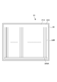
- FIG. 1 is a cross-sectional view showing a light control film according to the first embodiment of the present invention.
- This light control film 10 is formed by a film shape.
- the light control film 10 is a light control film that controls transmitted light using liquid crystal, and a liquid crystal material is formed by a lower laminate 13 and an upper laminate 12 that are first and second laminates in the form of a film, respectively.
- the liquid crystal cell 15 is a transverse electric field type liquid crystal cell that drives the liquid crystal molecules 14A related to the liquid crystal layer 14 by the IPS / FFS method, and the linear polarizing plates 16 and 17 are arranged in a crossed Nicols arrangement.
- the transparent electrode 22A according to the IPS / FFS method is formed on the entire surface of the base material 21A, and the transparent linear electrode 22B is sandwiched between the insulating layers 23. Then, an alignment layer 24A is provided. In the upper laminate 12 (the other laminate), the alignment layer 24B is provided on the base 21B.
- the first laminated body may constitute the upper laminated body 12, and the second laminated body may constitute the lower laminated body 13.
- the linear polarizing plates 16 and 17 are respectively provided with retardation films 18 and 19 for optical compensation on the liquid crystal cell 15 side.
- the retardation films 18 and 19 may be omitted as necessary.
- the light control film 10 controls the transmission of incident light by changing the orientation direction of the liquid crystal molecules 14A related to the liquid crystal layer 14 by changing the applied voltage between the electrodes 22A and 22B. And is configured to switch states.
- the light control film 10 is provided with a protective layer such as a hard coat layer on the surface of the linear polarizing plates 16 and 17 opposite to the liquid crystal cell 15.
- the light control film 10 is provided with spacer particles in the lower laminate 13 for keeping the thickness of the liquid crystal layer 14 constant.
- FIG. 2 is a diagram showing a detailed configuration of the spacer particles 27.
- the spacer particles 27 are so-called bead spacers that are spherical spacer particles.
- a transparent thin film layer 23 for fixing spacer particles is provided in the lower laminate 13, and spacer particles 27 that are buried in the transparent thin film layer 23 and define the thickness of the liquid crystal layer 14 are disposed.
- rod-shaped spacer particles may be applied.
- the insulating layer 23 between the electrodes 22A and 22B according to the IPS / FFS system is applied to the transparent thin film layer 23 for fixing the spacer particles (hereinafter, the transparent thin film layer 23 is referred to as the insulating layer 23).
- the transparent thin film layer 23 for fixing the spacer particles
- a sol-gel film made of an inorganic material such as SiO X can be applied.
- the spacer particles 27 are mixed in the coating solution of the insulating layer 23 so as to be sufficiently dispersed, and when the insulating layer 23 is manufactured, the surface of the electrode 22A is applied by applying the coating solution. Placed in. Further, by drying and curing the coating liquid in this state, the resin material related to the insulating layer 23 sufficiently enters between the electrode 22A and the spacer particle 27 while the spacer particle 27 is in contact with the electrode 22A. Harden.
- the insulating layer 23 is manufactured with a thickness of about 1 ⁇ m, while the spacer particles 27 have a diameter of 4 to 5 ⁇ m. Accordingly, in this embodiment, the spacer particles 27 are arranged so as to be buried in the insulating layer 23.
- the insulating layer 23 is coated by being dispersed in the coating solution of the insulating layer 23, and then dried and cured to produce the insulating layer 23, so that the insulating layer 23 is surrounded from the base side of the spacer particle 27 so as to surround the spacer particle 27.
- the resin material of the insulating layer 23 rises more than the thickness and is arranged around the spacer particles. As a result, the spacer particles 27 are held so as not to move to such an extent that the liquid crystal material related to the liquid crystal layer 14 is sandwiched and spread by the upper laminate 12 and the lower laminate 13.
- the transparent conductive layer related to the linear electrode 22 ⁇ / b> B is formed on the insulating layer 23 holding the spacer particles 27 in this manner, and then patterned to produce the linear electrode 22 ⁇ / b> B.
- the spacer particles 27 are arranged in a random position by being dispersed in the coating solution of the insulating layer 23, whereby the relative position between the linear electrode 22B and the spacer particles 27 changes variously. It is also expected that the electric field formation by the linear electrode 22B will be adversely affected.
- FIG. 3A shows a case where the spacer particles 27 having a diameter corresponding to the pitch of the linear electrodes 22B are arranged so that the centers thereof are the edges of the linear electrodes 22B.
- FIGS. 3A to 3C show the case where spacer particles 27 having a diameter corresponding to the width of the linear electrode 22B are used.
- the center of the spacer particles 27 is the linear electrode 22B.
- FIG. 3C shows the case where the spacer particles 27 are arranged so that the centers of the spacer particles 27 are located at the center between the linear electrodes 22B.
- the spacer particle fixing insulating layer 23 has a refractive index set to a value substantially equal to the refractive index of the electrodes 22A and 22B, and more specifically, the refractive index is 1.55 or more and 1.75. In the following, it is preferably set to 1.60 or more and 1.70 or less.
- ITO constituting the electrodes 22A and 22B has a refractive index of 1.858.
- a bridge B for short-circuiting the adjacent linear electrodes 22B is provided.
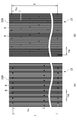
- FIG. 4 is a diagram showing the electrodes 22A and 22B in the lower laminate 13.
- the electrode 22A on the base 21A side is formed by forming a transparent conductive layer made of ITO on the entire surface of the base 21A, and power for driving is supplied from a power supply line (not shown).
- a power supply line (not shown).
- an insulating layer 23 is formed so as to cover the entire surface of the electrode 22A.
- the lower laminate 13 is provided with a power supply line 22BA to the linear electrode 22B at the end of the base 21A so as to extend along the long side of the base 21A, for example.
- the power supply line 22BA is formed of a metal material film having a small resistance value.
- the lower laminated body 13 is provided with linear electrodes 22B formed by patterning a transparent conductive layer with ITO at regular intervals so as to extend from the power supply line 22BA in a direction orthogonal to the power supply line 22BA. Driving power is supplied from the power supply line 22BA to the linear electrode 22B.
- the linear electrodes 22B are formed, for example, with an electrode width of 10 ⁇ m or less and an interval of 10 ⁇ m or less.
- the resistance value viewed from the power supply end of the linear electrode 22B increases as the distance from the base portion of the power supply line 22BA increases.
- the applied voltage to the liquid crystal layer decreases at the tip end side of the linear electrode, and as a result, there is a risk of uneven brightness.
- the light distribution of the liquid crystal material is controlled by the alternating electric field by applying an alternating power source in which the polarity of the driving power source is switched at regular time intervals to the electrodes 22 ⁇ / b> A and 22 ⁇ / b> B.
- the applied voltage of the liquid crystal layer is reduced on the tip side of the linear electrode 22B due to the resistance value of the linear electrode 22B, and uneven brightness occurs.
- the power supply lines of the linear electrodes 22B may be arranged along the long side on the other side, and more than three may be arranged at a constant pitch. Of course, it may be manufactured so as to extend along the short side.
- the resistance value can be reduced by shortening the length from the base portion of the power supply line 22BA to the tip side of the linear electrode 22B, thereby reducing the luminance value. Unevenness can be reduced. In addition, the frequency of malfunctions caused by disconnection can be reduced.
- a bridge B for short-circuiting adjacent linear electrodes 22B is provided at least in the middle of the extending direction of the linear electrodes 22B.
- the driving power can be transmitted and received between the adjacent linear electrodes 22B by the bridge B, so that the driving power can be supplied even if a disconnection occurs. Occurrence of difficult parts can be prevented, and generation of malfunctioning areas can be effectively avoided.
- the voltage of the driving power source in each part of the linear electrode 22B can be made uniform, thereby reducing the luminance unevenness.
- FIG. 5A a pair of adjacent linear electrodes 22B is sequentially manufactured, and a bridge B that short-circuits only the adjacent linear electrodes 22B is provided to the odd-numbered pair and the even-numbered pair, respectively.
- FIG. 6 is a diagram schematically showing a case in which an odd-numbered pair of bridges B and an even-numbered pair of bridges B are alternately provided in a direction in which the linear electrodes 22B extend at regular intervals. This is the case.
- the bridge B is repeatedly provided so that the pair of adjacent linear electrodes 22B has a repeated pitch TH of 1 mm.
- the bridge B is manufactured with a width that is a length in the extending direction of the linear electrode 22 being 5 ⁇ m or more and 15 ⁇ m or less.
- FIG. 5B is a diagram schematically showing a case where a bridge B that short-circuits only the adjacent linear electrodes 22B is provided, and the repeated pitch of the linear electrodes 22B in the continuous direction.
- the TW is set to 1 mm, and the position where the bridge B is provided is sequentially shifted in the linear electrode extending direction in the extending direction of the linear electrode.
- the pitch TH of the arrangement of the bridges B in the extending direction of the linear electrodes 22B is 1 mm.
- the bridge B is provided almost uniformly on the entire surface of the light control film 10, so that it is possible to effectively avoid the occurrence of a malfunctioning region due to disconnection, and to further reduce luminance unevenness.
- the bridges B may be arranged regularly or irregularly.
- permeability falls locally because the horizontal electric field used for light control cannot be formed between lower electrode 22A.
- the bridge B is manufactured with a length in the extending direction of the linear electrode 22B of 5 ⁇ m or more and 15 ⁇ m or less as in this embodiment, such a portion where the transmittance is locally reduced is extremely limited. Thus, a reduction in transmittance due to the provision of the bridge B can be effectively avoided.
- the light control film there is no restriction on the area for controlling the transmitted light depending on the size of the pixel as in the liquid crystal display panel, and the transmitted light in a wide area is controlled.
- the higher the number of bridges B arranged at a higher density the more uniform the voltage of the drive power supply at each part of the linear electrode 22B can be reduced.
- the transmittance is reduced at the site of the bridge B, if the number is arranged too much, the transmittance is significantly reduced. In addition, interference fringes may occur.
- the light control film has an interval of 10 mm or more and 100 mm or less which is at least several times the size of one pixel in the liquid crystal display panel in the extension direction of the linear electrodes between the linear electrodes (in FIG.
- the bridge B is repeatedly arranged, and this also effectively avoids a decrease in transmittance due to the provision of the bridge B, and further effectively avoids generation of interference fringes due to the bridge. Reduce unevenness.
- the bridge B may be manufactured so as to short-circuit only adjacent linear electrodes as in this embodiment, or may be manufactured so as to short-circuit three or more continuous linear electrodes.
- the number of linear electrodes can be variously set.
- each part As the base materials 21A and 21B, various transparent film materials having flexibility applicable to the liquid crystal cell 15 can be applied.
- the electrodes 22A and 22B can be widely applied to various configurations that are perceived as transparent.
- a transparent conductive film made of ITO Indium Tin Oxide
- ITO Indium Tin Oxide
- the electrode 22A is manufactured.
- a transparent conductive film made of ITO is manufactured on the entire surface of the base 21A, and then patterned to manufacture the linear electrode 22B.
- various transparent insulating materials applicable to this type of liquid crystal cell can be applied, and various inorganic materials and organic materials such as resin films can be applied.
- the alignment layers 24A and 24B are formed by applying various material layers applicable to the alignment layer such as polyimide and manufacturing a fine line-shaped uneven shape on the surface of the material layer by rubbing using a rubbing roll. .
- the alignment layer may be manufactured by manufacturing a fine line-shaped uneven shape manufactured by the rubbing process by the shaping process, or may be manufactured by the photo-alignment layer. Good.
- liquid crystal materials applied to this type of light control film can be widely applied to the liquid crystal layer 14.
- a liquid crystal material such as MLC 2166 manufactured by Merck Co., for example, can be applied to the liquid crystal layer 14.
- a sealing material 25 is disposed in a frame shape surrounding the liquid crystal layer 14, and leakage of liquid crystal related to the liquid crystal layer 14 is prevented by the sealing material 25, and the upper stacked body 12 and the lower stacked body 13 are further prevented.
- the sealing material 25 various materials capable of preventing the liquid crystal from leaking and holding the upper laminated body 12 and the lower laminated body 13 together can be applied.
- an epoxy resin is used as the sealing material 25.
- a thermosetting resin by an agent, an ultraviolet curable resin by an acrylic resin agent, a curable resin cured by heat and ultraviolet rays, or the like is applied.
- the linear polarizing plates 16 and 17 are so-called sheet polarizers, and after impregnating polyvinyl alcohol (PVA) with iodine or the like, an optical functional layer that performs an optical function as a polarizer is formed by stretching, and TAC (The optical functional layer is sandwiched between substrates made of a transparent film material such as triacetyl cellulose).
- PVA polyvinyl alcohol
- TAC TAC
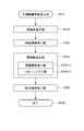
- FIG. 6 is a flowchart for explaining the manufacturing process of the light control film.
- the upper laminate 12 and the lower laminate 13 are manufactured in the upper laminate manufacturing process SP2 and the lower laminate manufacturing process SP3, respectively.
- the stacking step SP4 the upper stacked body 12 and the lower stacked body 13 are stacked with the liquid crystal layer 14 interposed therebetween, and then integrated with the seal material 25 to manufacture a liquid crystal cell.
- the liquid crystal cell thus manufactured is laminated and integrated with the linear polarizing plate to manufacture the light control film.
- FIG. 7 is a flowchart showing in detail the upper laminate manufacturing process SP2.
- the base layer 21B is coated with the coating liquid related to the alignment layer 24B and dried and cured, whereby the material of the alignment layer 24B.
- a layer is formed.
- a fine line-shaped uneven shape is manufactured on the surface of the alignment layer material layer by a rubbing process using a rubbing roll, whereby the alignment layer 24B is manufactured, and thus the upper laminate 12 is manufactured.
- a photo-alignment layer with a small stress applied during manufacturing is applied instead of the alignment layer by rubbing treatment. Is desirable.
- FIG. 8 is a flowchart showing in detail the lower laminate manufacturing process SP3.
- the transparent electrode 22A made of ITO is manufactured on the entire surface of the base 21A by sputtering.
- the insulating layer manufacturing process SP23 the insulating layer 23 is manufactured by applying a coating solution for the insulating layer 23, and then drying and curing.
- the spacer particles 27 are dispersed and mixed in the coating solution of the insulating layer 23, and thereby the spacer particles 27 are arranged so as to be embedded in the insulating layer 23.
- a spacer particle arrangement step is constituted by the insulating layer manufacturing step SP23.
- the linear electrode 22B is manufactured in the electrode manufacturing process SP24. More specifically, in this electrode manufacturing process SP24, the transparent conductive material related to the linear electrode 22B is deposited on the entire surface of the base material 21A by sputtering using a sputtering apparatus in the conductive layer manufacturing process SP24-1. A transparent conductive layer is produced. Further, the linear electrode 22B and the bridge B are manufactured by patterning in the subsequent patterning step SP24-2. Accordingly, in this embodiment, the bridge B can be manufactured without increasing the number of processes by effectively using the manufacturing process of the linear electrode.
- a coating layer related to the alignment layer 24A is applied, dried, and cured, thereby forming a material layer of the alignment layer 24A.
- a fine line-shaped uneven shape is manufactured on the surface of the alignment layer material layer by a rubbing process using a rubbing roll to manufacture the alignment layer 24A, and thus the lower laminate 13 is manufactured.
- the sealing material 25 is disposed using a dispenser in a frame shape surrounding the portion where the liquid crystal layer 14 is manufactured in the lower stacked body 13 or the upper stacked body 12. Thereafter, the liquid crystal material related to the liquid crystal layer 14 is dropped and disposed in a portion surrounded by the sealing material 25.
- the corresponding laminated body 13 or 12 is laminated on the laminated body 13 or 12 formed by arranging the liquid crystal material in this way, and then the laminated bodies 13 and 12 are pressed to obtain the liquid crystal material.
- the sealing material is semi-cured by irradiation with ultraviolet rays, and then heated to cure the sealing material.
- the laminates 12 and 13 are integrated so that the liquid crystal material does not leak.
- the step of pressing at least the laminates 13 and 12 to spread the liquid crystal material is performed under a reduced pressure environment, thereby preventing air from entering the liquid crystal layer. Even if it is in the process before and after this lamination process, it may be executed in a reduced pressure environment. On the contrary, if it is practically possible to prevent air from being mixed, the laminated bodies 13 and 12 are pressed. Then, the step of spreading the liquid crystal material may be performed under a normal pressure environment.
- the liquid crystal cell is manufactured by spreading the liquid crystal material by providing the transparent thin film layer for fixing the spacer particles and arranging the spacer particles embedded in the transparent thin film layer.
- the spacer particles can be prevented from moving, thereby preventing the spacer particles from being biased, and the cell gap can be uniformly produced by the spacer particles.
- the transparent thin film layer for fixing the spacer particles can be effectively used by using the configuration of the IPS / FFS method. Can be configured.
- the voltage of the driving power source in each part of the linear electrode can be made uniform, thereby reducing luminance unevenness.
- the transparent thin film layer 32 for fixing the spacer particles is preferably formed with a film thickness of 0.5 ⁇ m or less.
- the film thickness is preferably 0.1 ⁇ m or more and 0.5 ⁇ m or less.
- the transparent thin film layer 32 for fixing spacer particles has a refractive index of 1.55 or more and 1.75 or less, preferably 1.60 or more and 1.70 or less.
- the reflection at the interface with 21B is reduced to prevent a decrease in transmittance.
- FIG. 9 is a cross-sectional view showing a light control film according to the second embodiment in comparison with FIG.
- This light control film 30 is provided with a transparent thin film layer 32 for fixing spacer particles on the upper laminate 12, and is embedded in the transparent thin film layer 32 in the same manner as the insulating layer 23 according to the first embodiment. Spacer particles 27 are arranged.
- An alignment layer 24B is disposed on the liquid crystal layer 14 side of the transparent thin film layer 32.
- This embodiment has the same configuration as the above-described embodiment except that the configuration regarding the transparent thin film layer 32 is different.
- the same effect as that of the first embodiment can be obtained even when the spacer fine particles are arranged by providing a transparent thin film layer for fixing the spacer particles on the side where no electrode is arranged.
- an insulating layer having various values of volume resistivity can be applied to the transparent thin film layer 32 for fixing the spacer particles.
- the volume resistivity may be larger than 1 ⁇ 10 5 ⁇ m.
- the volume resistivity is set to 1 ⁇ 10 5 ⁇ m or less, the liquid crystal molecules in the liquid crystal layer 14 are disordered due to the influence of an electric field from the outside of the light control film due to static electricity or the like by ensuring appropriate conductivity. Therefore, dimming can be stably performed in various environments.
- FIG. 10 is a cross-sectional view showing a light control film according to the third embodiment in comparison with FIG.
- the alignment layer 24A of the lower laminate 13 constitutes a transparent thin film layer for fixing spacer particles, and the alignment layer 24A is formed in the same manner as the insulating layer 23 according to the first embodiment.
- Spacer particles 27 are arranged so as to be buried.
- the photo-alignment layer is applied to the alignment layer, and spacer particles are dispersed and mixed in the photo-alignment layer coating solution instead of the insulating layer coating solution, thereby forming the photo-alignment layer.
- spacer fine particles are dispersed and arranged.
- the photo-alignment layer is applied to the transparent thin film layer for fixing the spacer particles, and the spacer fine particles are embedded by the photo-alignment layer so as to be difficult to move.
- This embodiment is configured in the same manner as the first embodiment or the second embodiment except that the buried layer of the spacer fine particles is different.
- the transparent thin film layer (alignment layer 24A) preferably has a refractive index of 1.55 or more and 1.75 or less, more preferably 1.60 or more and 1.70 or less. It consists of alumina.
- the transparent thin film layer has a refractive index between the liquid crystal layer 14 (for example, a refractive index of about 1.5) and the linear electrode 22B (for example, a refractive index of 1.858 for ITO), and a refractive index adjusting layer (index matching layer). )
- the linear electrode 22B for example, a refractive index of 1.858 for ITO
- FIG. 11 is a cross-sectional view showing a light control film according to the fourth embodiment in comparison with FIG.
- insulating layers 23A and 23B having a laminated structure of a plurality of layers (insulating layers) 23A and 23B are provided between the transparent electrode 22A and the linear electrode 22B.
- This embodiment has the same configuration as that of the above-described embodiment except that the configuration regarding the insulating layers 23A and 23B is different.
- the laminated structure of the plurality of layers is constituted by a two-layer laminated structure of the first and second insulating layers 23B and 23A. Therefore, a laminated structure of three or more layers may be used.
- the cell gap can be finely adjusted by adjusting the ratio of the thicknesses of the plurality of layers 23B and 23A, thereby improving the yield.
- the coating is performed on the transparent electrode 22A by the first insulating layer manufacturing process.
- the coating liquid is applied and dried to produce the first insulating layer 23B
- the coating liquid is applied and dried on the first insulating layer 23B by the second insulating layer manufacturing process.
- Two insulating layers 23A are manufactured.
- the thickness of the first insulating layer 23B is measured discretely or continuously, and the coating conditions relating to the second insulating layer 23A are adjusted based on the measurement result, thereby finely adjusting the cell gap.
- the cell gap is ensured with high accuracy.
- the cell gap is the distance between the alignment layers 24A and 24B in a region where the linear electrode 22B is not formed.
- the alignment layers 24A and 24B are substantially thin due to the small thickness. It becomes the space
- an insulating layer is formed by a laminated structure of a plurality of layers 23A and 23B in this way, and the light control film 50 includes a layer 23A that is the outermost layer on the liquid crystal layer 14 side of the plurality of layers 23A and 23B. It is assigned to the transparent thin film layer for fixing the spacer particles, and the spacer particles 27 are fixed and held on the substrate by the outermost layer 23A.
- spacer particles are dispersed and mixed in the coating liquid in the step of forming the first insulating layer.
- the first insulating layer 23A which is a transparent thin film layer for fixing spacer particles, is formed with a film thickness of 0.5 ⁇ m or less, and this occurs when spacer particles are arranged. An increase in haze value due to the undulation of the transparent thin film layer is suppressed.
- the same effect as that of the above-described embodiment can also be obtained by forming the insulating layer into a multilayer structure including a plurality of layers and holding the spacer particles in the outermost layer. Furthermore, the cell gap can be finely adjusted, and further the risk of conduction due to pinholes can be reduced. Also, compared to the case where the spacer layer is fixed by constituting an insulating layer with a single layer, the protruding ratio of the spacer particle is increased, and as a result, the spacer size is reduced and the transmittance loss due to the spacer is reduced. And the risk of disconnection of the linear electrode can be reduced.
- the transparent thin film layer for fixing the spacer particles has a thickness of 0.5 ⁇ m or less, an increase in haze value can be suppressed.
- the present invention is not limited to this, and the present invention is widely applied to the case where the linear electrode is manufactured by bending the linear electrode. can do.
- the spacer particles are arranged in any of the first and second laminates.
- the present invention is not limited thereto, and the first embodiment may be combined with the configuration of the above-described embodiment. You may make it arrange
- Light control film 12 Upper laminated body 13 Lower laminated body 14 Liquid crystal layer 14A Liquid crystal molecule 15 Liquid crystal cell 16, 17 Linearly polarizing plate 18, 19 Retardation film 21A, 21B Substrate 22A Electrode 22B Linear Electrode 22BA power supply line 23, 23A, 23B Transparent thin film layer (insulating layer) 24A, 24B Alignment layer 25 Sealing material 27 Spacer particles
Landscapes
- Physics & Mathematics (AREA)
- Nonlinear Science (AREA)
- Chemical & Material Sciences (AREA)
- Crystallography & Structural Chemistry (AREA)
- General Physics & Mathematics (AREA)
- Optics & Photonics (AREA)
- Mathematical Physics (AREA)
- Liquid Crystal (AREA)
Abstract
液晶材料を押し広げて液晶セルを製造する場合にあっても、スペーサー粒子を使用してセルギャップを均一に製造することができるようにする。 第1及び第2の積層体13、12により液晶層14を挟持し、液晶層14に係る液晶分子14Aの配向を制御して透過光を制御するIPS/FFS方式の調光フィルム10において、第1の積層体13には、スペーサー粒子固定用の透明薄膜層23が設けられ、透明薄膜層23に埋没して液晶層14の厚みに係るスペーサー粒子27が配置されている。
Description
本発明は、乗用車の窓等に貼り付けて外来光の透過を制御する調光フィルムに関する。
従来、例えば窓に貼り付けて外来光の透過を制御する調光フィルムに関する工夫が種々に提案されている(特許文献1、2)。このような調光フィルムの1つに、液晶を利用したものがある。この液晶を利用した調光フィルムは、透明電極を製造した透明フィルム材により液晶材料を挟持して液晶セルが製造され、この液晶セルを直線偏光板により挟持して作成される。これによりこの調光フィルムでは、液晶に印加する電界の可変により液晶の配向を可変して外来光を遮光したり透過したりし、さらには透過光量を可変したりし、これらにより外来光の透過を制御する。
この液晶セルの駆動には、液晶表示パネルについて提案されている種々の駆動方法を適用することができる。具体的には、例えばTN(Twisted Nematic)方式、IPS(In-Place-Switching)方式、VA(Virtical Alignment)方式等の駆動方式を適用することができる。しかしながら調光フィルムでは、例えば窓ガラスに貼り付けて種々の方向より見て取られる特長がある。これにより視野角依存性の少ないIPS方式により駆動することが好ましいと考えられる。
またこのIPS方式のうちの、FFS(フリンジフィールドスイッチング)方式(IPS/FFS方式)によれば、透過率を高くすることができ、これによりこの種の調光フィルムにおける液晶セルの駆動に適用して好ましいと考えられる。ここでIPS/FFS方式は、液晶層を挟持する1対の基材のうちの一方の基材に駆動用の透明電極をまとめて製造する構成である。IPS/FFS方式では、この一方の基材の全面に、透明電極を製造した後、絶縁層を間に挟んで一定のピッチにより線状電極を製造し、この全面の透明電極と線状電極との間で発生する基材表面の面内方向の電界であるいわゆる横電界により液晶の配向を制御する。
液晶表示パネルにおいては、液晶セルの厚みであるセルギャップを調整する方法として、ビーズ状又はロッド状のスペーサー粒子を散布する方法が提案されており、特許文献3には、このスペーサー粒子の配置に関する工夫が提案されている。
ところで調光フィルムでは、可撓性を有する透明フィルム材により液晶材料を挟持して大面積の液晶セルを構成する。これにより減圧した環境において、液晶材料を間に挟んで透明フィルム材により押圧して液晶材料を押し広げることにより、大面積の液晶セルを効率良く作成できると考えられる。しかしながらこのように液晶材料を押し広げて液晶セルを製造する場合、透明フィルム材に散布したスペーサー粒子が移動してスペーサー粒子の配置に偏りが発生する。これによりこの場合、セルギャップを均一に製造することが困難になる問題がある。
本発明はこのような状況に鑑みてなされたものであり、液晶材料を押し広げて液晶セルを製造する場合にあっても、スペーサー粒子を使用してセルギャップを均一に製造することができるようにする。
本発明者は、上記課題を解決するために鋭意研究を重ね、スペーサー粒子固定用の透明薄膜層を設け、この透明薄膜層によりスペーサー粒子を移動困難に配置する、との着想に至り、本発明を完成するに至った。
具体的には、本発明では、以下のようなものを提供する。
(1) 第1及び第2の積層体により液晶層を挟持し、
一方の積層体には、透明フィルム材による基材上に透明電極が設けられ、絶縁層を間に挟んで前記透明電極上に線状電極が設けられる調光フィルムにおいて、
前記第1及び/又は第2の積層体には、スペーサー粒子固定用の透明薄膜層が設けられ、前記透明薄膜層に埋没して前記液晶層の厚みに係るスペーサー粒子が設けられた
調光フィルム。
一方の積層体には、透明フィルム材による基材上に透明電極が設けられ、絶縁層を間に挟んで前記透明電極上に線状電極が設けられる調光フィルムにおいて、
前記第1及び/又は第2の積層体には、スペーサー粒子固定用の透明薄膜層が設けられ、前記透明薄膜層に埋没して前記液晶層の厚みに係るスペーサー粒子が設けられた
調光フィルム。
(1)によれば、スペーサー粒子を移動困難に配置することにより、液晶材料を押し広げて液晶セルを製造する場合にあっても、スペーサー粒子の移動を防止することができ、これによりスペーサー粒子の配置の偏りを防止して、スペーサー粒子によりセルギャップを均一に製造することができる。
(2) (1)において、
前記スペーサー粒子固定用の透明薄膜層が、前記絶縁層である調光フィルム。
前記スペーサー粒子固定用の透明薄膜層が、前記絶縁層である調光フィルム。
(2)によれば、IPS/FFS方式に適用して、このIPS/FFS方式の構成における電極間の絶縁層を有効利用して、スペーサー粒子固定用の透明薄膜層を構成することができる。
(3) (2)において、
前記絶縁層が、複数の層の積層構造による絶縁層であり、
前記スペーサー粒子固定用の透明薄膜層が、前記絶縁層の複数の層のうちの、前記液晶層の側の最表層の層である調光フィルム。
前記絶縁層が、複数の層の積層構造による絶縁層であり、
前記スペーサー粒子固定用の透明薄膜層が、前記絶縁層の複数の層のうちの、前記液晶層の側の最表層の層である調光フィルム。
(3)によれば、前記絶縁層に係る複数の層の厚さの比率を調整することで、セルギャップを微調整する事ができる。またピンホールによる導通のリスクを低減することができる。さらに単層により絶縁層を構成してスペーサー粒子を固定する場合に比して、スペーサー粒子の突出する割合が大きくなり、その結果、スペーサーのサイズを小さくすることができ、スペーサーによる透過率ロスを小さくすることができ、線状電極の断線のリスクを低減することができる。
(4) (1)において、
前記一方の積層体は、
前記線状電極上に第1の配向層が設けられ、
他方の積層体は、
透明フィルム材による基材上に第2の配向層が設けられ、
前記スペーサー粒子固定用の透明薄膜層が、前記第2の配向層である調光フィルム。
前記一方の積層体は、
前記線状電極上に第1の配向層が設けられ、
他方の積層体は、
透明フィルム材による基材上に第2の配向層が設けられ、
前記スペーサー粒子固定用の透明薄膜層が、前記第2の配向層である調光フィルム。
(4)によれば、配向層を有効利用して、スペーサー粒子固定用の透明薄膜層を構成することができる。
(5) (1)から(4)において、
前記スペーサー粒子固定用の透明薄膜層の膜厚が0.5μm以下である調光フィルム。
前記スペーサー粒子固定用の透明薄膜層の膜厚が0.5μm以下である調光フィルム。
(5)によれば、前記スペーサー粒子固定用の透明薄膜層を使用してスペーサー粒子を配置する際に発生する当該透明薄膜層の起伏によるヘイズ値の増加を抑制することができる。
(6) (1)から(5)において、
前記一方の積層体において、
前記スペーサー粒子固定用の透明薄膜層は、
屈折率が1.55以上1.75以下である調光フィルム。
前記一方の積層体において、
前記スペーサー粒子固定用の透明薄膜層は、
屈折率が1.55以上1.75以下である調光フィルム。
(6)によれば、スペーサー粒子固定用の透明薄膜層の界面における反射を低減して透過率を向上することができる。
(7) (1)から(6)において、
隣接する線状電極を短絡するブリッジが、少なくとも線状電極の延長方向の途中に設けられた調光フィルム。
隣接する線状電極を短絡するブリッジが、少なくとも線状電極の延長方向の途中に設けられた調光フィルム。
(7)によれば、ブリッジにより隣接する線状電極間で駆動用電源を相互に送受できることにより、スペーサー粒子の配置により線状電極が断線した場合にあっても、駆動用電源の供給が困難になる箇所の発生を防止することができ、これにより動作不良の領域の発生を有効に回避することができる。またブリッジを設けることにより線状電極の各部における駆動用電源の電圧も均一化することができ、これにより輝度ムラを低減することができる。
(8) 第1及び第2の積層体により液晶層を挟持し、前記液晶層に係る液晶分子の配向を制御して透過光を制御するIPS/FFS方式の調光フィルムの製造方法において、
前記第1の積層体を製造する第1の積層体製造工程を備え、
前記第1の積層体製造工程は、
スペーサー粒子を分散した透明薄膜材料の塗工液を前記第1の積層体に係る透明基材に塗工して乾燥させ、前記スペーサー粒子を移動困難に前記透明薄膜材料の層により前記透明基材に配置するスペーサー粒子配置工程を備える調光フィルムの製造方法。
前記第1の積層体を製造する第1の積層体製造工程を備え、
前記第1の積層体製造工程は、
スペーサー粒子を分散した透明薄膜材料の塗工液を前記第1の積層体に係る透明基材に塗工して乾燥させ、前記スペーサー粒子を移動困難に前記透明薄膜材料の層により前記透明基材に配置するスペーサー粒子配置工程を備える調光フィルムの製造方法。
(8)によれば、スペーサー粒子を移動困難に第1の積層体に配置することにより、液晶材料を押し広げて液晶セルを製造する場合にあっても、スペーサー粒子の移動を防止することができ、これによりスペーサー粒子の配置の偏りを防止して、スペーサー粒子によりセルギャップを均一に製造することができる。
(9) (8)において、
前記第1の積層体製造工程は、
前記透明基材に透明電極を製造する透明電極製造工程と、
前記透明電極の上に絶縁層を製造する絶縁層製造工程と、
前記絶縁層の上に、線状電極を製造する線状電極製造工程を備え、
前記スペーサー粒子配置工程は、
前記絶縁層の塗工液に前記スペーサー粒子を分散させて、前記絶縁層製造工程により前記スペーサー粒子を配置する調光フィルムの製造方法。
前記第1の積層体製造工程は、
前記透明基材に透明電極を製造する透明電極製造工程と、
前記透明電極の上に絶縁層を製造する絶縁層製造工程と、
前記絶縁層の上に、線状電極を製造する線状電極製造工程を備え、
前記スペーサー粒子配置工程は、
前記絶縁層の塗工液に前記スペーサー粒子を分散させて、前記絶縁層製造工程により前記スペーサー粒子を配置する調光フィルムの製造方法。
(9)によれば、IPS/FFS方式に適用して、このIPS/FFS方式の構成における電極間の絶縁層を有効利用して、スペーサー粒子固定用の透明薄膜層を構成することができる。
(10) (9)において、
前記第1の積層体製造工程は、
前記透明基材に透明電極を製造する透明電極製造工程と、
前記透明電極の上に第1の絶縁層を製造する第1の絶縁層製造工程と、
前記第1の絶縁層の上に第2の絶縁層を製造する第2の絶縁層製造工程と、
前記第2の絶縁層の上に、線状電極を製造する線状電極製造工程を備え、
前記スペーサー粒子配置工程は、
前記第2の絶縁層の塗工液に前記スペーサー粒子を分散させて、前記第2の絶縁層製造工程により前記スペーサー粒子を配置する調光フィルムの製造方法。
前記第1の積層体製造工程は、
前記透明基材に透明電極を製造する透明電極製造工程と、
前記透明電極の上に第1の絶縁層を製造する第1の絶縁層製造工程と、
前記第1の絶縁層の上に第2の絶縁層を製造する第2の絶縁層製造工程と、
前記第2の絶縁層の上に、線状電極を製造する線状電極製造工程を備え、
前記スペーサー粒子配置工程は、
前記第2の絶縁層の塗工液に前記スペーサー粒子を分散させて、前記第2の絶縁層製造工程により前記スペーサー粒子を配置する調光フィルムの製造方法。
(10)によれば、第1及び第2の絶縁層に係る複数の層の厚さの比率を調整することで、セルギャップを微調整する事ができる。またピンホールによる導通のリスクを低減することができる。さらに単層によりスペーサー粒子を固定する場合に比して、スペーサー粒子の突出する割合が大きくなり、その結果、スペーサーのサイズを小さくすることができ、スペーサーによる透過率ロスを小さくすることができ、線状電極の断線のリスクを低減することができる。
(11) (10)において、
前記第1の積層体製造工程は、
前記透明基材に配向層を製造する配向層製造工程を備え、
前記スペーサー粒子配置工程は、
前記配向層の塗工液に前記スペーサー粒子を分散させて、前記配向層製造工程により前記スペーサー粒子を配置する調光フィルムの製造方法。
前記第1の積層体製造工程は、
前記透明基材に配向層を製造する配向層製造工程を備え、
前記スペーサー粒子配置工程は、
前記配向層の塗工液に前記スペーサー粒子を分散させて、前記配向層製造工程により前記スペーサー粒子を配置する調光フィルムの製造方法。
(11)によれば、配向層を有効利用して、さらには配向層製造工程を有効利用して、スペーサー粒子固定用の透明薄膜層を構成することができる。
(12) (8)から(11)において、
前記液晶層に係る液晶材料を前記第1及び第2の積層体により押し広げて液晶セルを製造する積層工程を備える調光フィルムの製造方法。
前記液晶層に係る液晶材料を前記第1及び第2の積層体により押し広げて液晶セルを製造する積層工程を備える調光フィルムの製造方法。
(12)によれば、液晶材料を押圧して押し広げるようにして、大面積の液晶セルを効率良く作成するようにして、スペーサー粒子の配置の偏りを有効に回避してセルギャップを均一に製造することができる。
本発明によれば、液晶材料を押し広げて液晶セルを製造する場合にあっても、スペーサー粒子を使用してセルギャップを均一に製造することができる。
〔第1実施形態〕
図1は、本発明の第1実施形態に係る調光フィルムを示す断面図である。この調光フィルム10は、フィルム形状により形成される。この調光フィルム10は、液晶を利用して透過光を制御する調光フィルムであり、それぞれフィルム形状の第1及び第2の積層体である下側積層体13及び上側積層体12により液晶材料を挟持して液晶セル15が製造され、この液晶セル15を直線偏光板16、17により挟持して作成される。ここで液晶セル15は、IPS/FFS方式により液晶層14に係る液晶分子14Aを駆動する横電界方式の液晶セルであり、直線偏光板16、17がクロスニコル配置により配置される。これにより下側積層体13(一方の積層体)は、基材21Aの全面に、IPS/FFS方式に係る透明電極22Aが形成され、絶縁層23を間に挟んで透明の線状電極22Bが形成され、続いて配向層24Aが設けられる。また上側積層体12(他方の積層体)は、基材21Bに配向層24Bが設けられる。なお、本発明においては、第1の積層体が上側積層体12を構成し、第2の積層体が下側積層体13を構成してもよい。
図1は、本発明の第1実施形態に係る調光フィルムを示す断面図である。この調光フィルム10は、フィルム形状により形成される。この調光フィルム10は、液晶を利用して透過光を制御する調光フィルムであり、それぞれフィルム形状の第1及び第2の積層体である下側積層体13及び上側積層体12により液晶材料を挟持して液晶セル15が製造され、この液晶セル15を直線偏光板16、17により挟持して作成される。ここで液晶セル15は、IPS/FFS方式により液晶層14に係る液晶分子14Aを駆動する横電界方式の液晶セルであり、直線偏光板16、17がクロスニコル配置により配置される。これにより下側積層体13(一方の積層体)は、基材21Aの全面に、IPS/FFS方式に係る透明電極22Aが形成され、絶縁層23を間に挟んで透明の線状電極22Bが形成され、続いて配向層24Aが設けられる。また上側積層体12(他方の積層体)は、基材21Bに配向層24Bが設けられる。なお、本発明においては、第1の積層体が上側積層体12を構成し、第2の積層体が下側積層体13を構成してもよい。
直線偏光板16、17は、それぞれ液晶セル15側に光学補償に供する位相差フィルム18、19が設けられる。なお位相差フィルム18、19は、必要に応じて省略してもよい。これによりこの調光フィルム10は、電極22A、22B間の印加電圧の可変により、液晶層14に係る液晶分子14Aの配向方向を可変して入射光の透過を制御し、例えば透過状態と遮光状態とで状態を切り替えるように構成される。なお調光フィルム10は、直線偏光板16、17の液晶セル15とは逆側の面に、ハードコート層等による保護層が設けられる。
調光フィルム10には、液晶層14の厚みを一定に保持するためのスペーサー粒子が下側積層体13に設けられる。
〔スペーサーの配置〕
図2は、このスペーサー粒子27の詳細構成を示す図である。スペーサー粒子27は、球形状によるスペーサー粒子であるいわゆるビーズスペーサーである。調光フィルム10では、スペーサー粒子固定用の透明薄膜層23が下側積層体13に設けられ、この透明薄膜層23に埋没して液晶層14の厚みを規定するスペーサー粒子27が配置される。なおビーズ形状のスペーサー粒子に代えて、ロッド形状のスペーサー粒子を適用してもよい。
図2は、このスペーサー粒子27の詳細構成を示す図である。スペーサー粒子27は、球形状によるスペーサー粒子であるいわゆるビーズスペーサーである。調光フィルム10では、スペーサー粒子固定用の透明薄膜層23が下側積層体13に設けられ、この透明薄膜層23に埋没して液晶層14の厚みを規定するスペーサー粒子27が配置される。なおビーズ形状のスペーサー粒子に代えて、ロッド形状のスペーサー粒子を適用してもよい。
ここでこの実施形態においては、このスペーサー粒子固定用の透明薄膜層23にIPS/FFS方式に係る電極22A、22B間の絶縁層23が適用され(以下、透明薄膜層23を絶縁層23と標記する場合がある)、これによりこのIPS/FFS方式に係る構成を有効に利用してスペーサー粒子27を移動困難とする。なおスペーサー粒子固定用の透明薄膜層としては、例えば、SiOXなどの無機材料によるゾルゲル膜を適用できる。
すなわちこの実施形態において、スペーサー粒子27は、充分に分散するようにして絶縁層23の塗工液に混入され、絶縁層23を製造する際にこの塗工液の塗工により、電極22Aの表面に配置される。またこの状態でこの塗工液を乾燥、硬化させることにより、スペーサー粒子27が電極22Aに接触する状態で、絶縁層23に係る樹脂材が電極22Aとスペーサー粒子27の間に充分に侵入して硬化する。ここで絶縁層23は、厚み1μm程度により製造されるのに対し、スペーサー粒子27は、直径が4~5μmである。これによりこの実施形態では絶縁層23に埋没するようにスペーサー粒子27が配置される。
またさらに絶縁層23の塗工液に分散させて塗工した後、乾燥、硬化させて絶縁層23を製造することにより、スペーサー粒子27を囲むようにスペーサー粒子27の付け根側から絶縁層23の厚み以上に絶縁層23の樹脂材が立ち上がってスペーサー粒子の周囲に配置される。これにより上側積層体12及び下側積層体13により液晶層14に係る液晶材料を挟持して押し広げる程度では、移動しないようにスペーサー粒子27が保持される。
調光フィルム10は、このようにスペーサー粒子27を保持してなる絶縁層23の上に、線状電極22Bに係る透明導電層が製膜された後、パターニングして線状電極22Bが製造される。ここでスペーサー粒子27は、絶縁層23の塗工液に分散して配置されることにより、ランダムな位置に配置され、これにより線状電極22Bとスペーサー粒子27との相対位置は種々に変化し、線状電極22Bによる電界形成に悪影響を与えることも予測される。
これにより図3に示すように、スペーサー粒子27に対して線状電極22Bの相対位置を種々に変化させて横電界を検討した。ここでスペーサー粒子27の影響により横電界に異常が発生するのは、スペーサー粒子27の周辺の極めて狭い領域であることが判った。これに対してスペーサー粒子27は、直径4~5μm程度の小径であり、これによりこのような横電界の異常による透過光への影響は極めて小さいことが確認された。ここで図3(A)は、線状電極22Bのピッチに対応する直径によるスペーサー粒子27が、その中心が線状電極22Bのエッジとなるように配置された場合である。また図3(B)及び(C)は、線状電極22Bの幅による直径のスペーサー粒子27を使用した場合であり、図3(B)は、このスペーサー粒子27の中心が、線状電極22Bの幅方向の中心となるように配置された場合であり、図3(C)は、このスペーサー粒子27の中心が、線状電極22B間の中心に位置するように配置された場合である。これら図3(A)~(C)のシミュレーションにより、スペーサー粒子27に線状電極22Bが部分的にでも重なった場合には、液晶の配向に供する横電界が局所的に乱れるものの、その範囲が極めて狭い領域であることが確認された。
さらにこの実施形態において、スペーサー粒子固定用の絶縁層23は、屈折率が、電極22A、22Bの屈折率とほぼ等しい値に設定され、より具体的には屈折率が1.55以上1.75以下に、好ましくは1.60以上1.70以下に設定される。ここで電極22A、22Bを構成するITOは、屈折率が1.858である。これにより調光フィルム1は、絶縁層23と電極22A、22Bとの界面、絶縁層23と配向層24Aとの界面で、透過光の反射を低減し、透過率の低下を防止する。
〔ブリッジ〕
またこのようにスペーサー粒子27を保持してなる絶縁層23の上に、線状電極22Bに係る透明導電層を製膜した後、パターニングして線状電極22Bを製造する場合、スペーサー粒子27上で線状電極22Bが局所的に断線する恐れがある。調光フィルム10において、この線状電極が局所的に断線すると、この断線した部位より先端側(電源より遠い側)では、駆動用の電源が供給されないことになる。これによりこのような部位では、液晶駆動用の電界を製造して調光することが困難になり、これにより動作不良の領域が発生することになる。特に、調光フィルムでは、大面積の領域で調光を図ることにより、断線により調光することができない動作不良領域も大面積により発生することになる。
またこのようにスペーサー粒子27を保持してなる絶縁層23の上に、線状電極22Bに係る透明導電層を製膜した後、パターニングして線状電極22Bを製造する場合、スペーサー粒子27上で線状電極22Bが局所的に断線する恐れがある。調光フィルム10において、この線状電極が局所的に断線すると、この断線した部位より先端側(電源より遠い側)では、駆動用の電源が供給されないことになる。これによりこのような部位では、液晶駆動用の電界を製造して調光することが困難になり、これにより動作不良の領域が発生することになる。特に、調光フィルムでは、大面積の領域で調光を図ることにより、断線により調光することができない動作不良領域も大面積により発生することになる。
そこでこの実施形態では、隣接する線状電極22Bを短絡するブリッジBが設けられる。
〔線状電極の構成〕
図4は、下側積層体13における電極22A、22Bを示す図である。この実施形態において、基材21A側の電極22Aは、基材21Aの全面にITOによる透明導電層が製造されて形成され、図示しない電源供給ラインにより駆動用の電源が供給される。さらに下側積層体13は、この電極22Aの全面を覆うように絶縁層23が形成される。下側積層体13は、例えば基材21Aの長辺に沿って延長するように、基材21Aの端部に線状電極22Bへの電源供給ライン22BAが形成される。ここで電源供給ライン22BAは、抵抗値の小さな金属材料膜等により形成される。下側積層体13は、この電源供給ライン22BAからこの電源供給ライン22BAと直交する方向に延長するように、ITOによる透明導電層のパターンニングによる線状電極22Bが一定の間隔により設けられ、この線状電極22Bに電源供給ライン22BAから駆動用電源が供給される。なお線状電極22Bは、例えば電極幅10μm以下の微細幅により、10μm以下の間隔で配置して形成される。
図4は、下側積層体13における電極22A、22Bを示す図である。この実施形態において、基材21A側の電極22Aは、基材21Aの全面にITOによる透明導電層が製造されて形成され、図示しない電源供給ラインにより駆動用の電源が供給される。さらに下側積層体13は、この電極22Aの全面を覆うように絶縁層23が形成される。下側積層体13は、例えば基材21Aの長辺に沿って延長するように、基材21Aの端部に線状電極22Bへの電源供給ライン22BAが形成される。ここで電源供給ライン22BAは、抵抗値の小さな金属材料膜等により形成される。下側積層体13は、この電源供給ライン22BAからこの電源供給ライン22BAと直交する方向に延長するように、ITOによる透明導電層のパターンニングによる線状電極22Bが一定の間隔により設けられ、この線状電極22Bに電源供給ライン22BAから駆動用電源が供給される。なお線状電極22Bは、例えば電極幅10μm以下の微細幅により、10μm以下の間隔で配置して形成される。
これにより調光フィルム10では、スペーサー粒子27の配置により線状電極22Bが途中で断線すると、この断線した部位より先端側で液晶材料を駆動できなくなり、動作不良の領域が発生することになる。
なおこのように線状電極を形成して大面積の領域で調光を図る場合、線状電極22Bでは、電源供給ライン22BAの付け根部分にから遠ざかるに従って電源供給端から見た抵抗値が増大することにより、液晶層への印可電圧が線状電極の先端側で低下し、その結果、輝度ムラが発生する恐れがある。なお調光フィルム10では、一定の時間間隔で駆動用電源の極性が切り替わる交番電源を電極22A、22Bに印加することにより、交番電界により液晶材料の配光を制御する。これにより線状電極22Bの抵抗値により線状電極22Bの先端側で液晶層の印可電圧が低下し、輝度ムラが発生する。
なお基材21A側の電極22Aにあっても、線状電極22Bと同様に電源供給ラインを設けて駆動用電源を供給してもよい。また線状電極22Bの電源供給ラインは、電源供給ライン22BAに加えて、他方の側の長辺に沿って配置するようにしてもよく、さらには一定のピッチにより3本以上配置してもよく、また当然に短辺に沿って延長するように製造してもよい。このようにして電源供給ライン22BAの本数を増大させると、線状電極22Bに係る電源供給ライン22BAの付け根部分から先端側までの長さを短くして抵抗値を小さくすることができることにより、輝度ムラを低減することができる。また断線により発生する動作不良の頻度を低減することができる。
この実施形態では、図5(A)及び(B)により示すように、隣接する線状電極22Bを短絡するブリッジBを、少なくとも線状電極22Bの延長方向の途中に設ける。このようにブリッジBを設けた場合には、このブリッジBにより隣接する線状電極22B間で駆動用電源を相互に送受できることにより、断線が発生した場合にあっても、駆動用電源の供給が困難になる箇所の発生を防止することができ、これにより動作不良の領域の発生を有効に回避することができる。またこのようにブリッジBを設けることにより線状電極22Bの各部における駆動用電源の電圧も均一化することができ、これにより輝度ムラを低減することができる。
ここで図5(A)は、隣接する線状電極22Bによる対を順次製造して、奇数番目の対と偶数番目の対とに、それぞれ隣接する線状電極22Bのみを短絡させるブリッジBを設ける場合を模式的に示す図であり、奇数番目の対に係るブリッジBと偶数番目の対に係るブリッジBとを、線状電極22Bの延長する方向に、一定の間隔を隔てて順次交互に設けた場合である。この図3(A)の例では、線状電極22Bの連続する方向には、ピッチTW=1mmによりブリッジBを繰り返し設ける。また線状電極22Bの延長方向では、隣接する線状電極22Bの対で、繰り返しのピッチTHが1mmになるようにブリッジBを繰り返し設ける。ここでブリッジBは、線状電極22の延長方向に係る長さである幅が5μm以上15μm以下により製造される。
これに対して図5(B)は、同様に隣接する線状電極22Bのみを短絡させるブリッジBを設ける場合を模式的に示す図であり、線状電極22Bの連続する方向への繰り返しのピッチTWを1mmとし、線状電極の延長方向で、ブリッジBを設ける箇所を線状電極の繰り返し方向に順次シフトさせたものである。なおこの図3(B)において、隣接する線状電極22Bの対に関して、この線状電極22Bの延長方向に係るブリッジBの配置のピッチTHは1mmである。
なおブリッジBは、調光フィルム10の全面にほぼ均一に設けるようにして、断線による動作不良の領域の発生を有効に回避することができ、さらには輝度ムラを低減することができる。またブリッジBは規則的に配置してもよく、不規則に配置してもよい。なおブリッジBを設けた箇所では、下層の電極22Aとの間で調光に供する横電界を形成できないことにより、局所的に透過率が低下することになる。しかしながらこの実施形態のように線状電極22Bの延長方向に係る長さが5μm以上15μm以下によりブリッジBを製造する場合には、このような局所的に透過率が低下する部位は、極めて限られた小面積の領域とすることができ、これによりブリッジBを設けたことによる透過率の低下を有効に回避することができる。
また調光フィルムでは、液晶表示パネルのような画素の大きさによる透過光を制御する領域の制限が無く、広い領域の透過光を制御することになる。これによりブリッジBを高密度に多数配置すればする程、線状電極22Bの各部における駆動用電源の電圧も均一化することができ、これにより輝度ムラを低減することができる。しかしながらブリッジBの部位で透過率が低下することにより、余りに多く配置すると、透過率の低下が著しくなる。また干渉縞が発生する恐れもある。そこで調光フィルムは、各線状電極間において、線状電極の延長方向に、少なくとも液晶表示パネルにおける1画素の大きさの数倍以上である10mm以上100mm以下の間隔(図5において、符号Tで示す間隔である)で繰り返しブリッジBが配置され、これによってもブリッジBを設けたことによる透過率の低下を有効に回避し、さらにはブリッジによる干渉縞の発生等を有効に回避して、輝度ムラを低減する。
またブリッジBは、この実施形態のように隣接する線状電極のみを短絡するように製造してもよく、連続する3本以上の線状電極を短絡させるように製造してもよく、短絡させる線状電極の本数にあっては種々に設定することができる。
〔各部の詳細構成〕
基材21A、21Bは、液晶セル15に適用可能な可撓性を有する各種の透明フィルム材を適用することができ、この実施形態では、両面にハードコート層が製造されてなるポリカーボネート等によるフィルム材が適用される。電極22A、22Bは、透明と知覚される種々の構成を広く適用することができ、この実施形態では、透明電極材であるITO(Indium Tin Oxide)による透明導電膜を基材21Aの全面に製造して電極22Aが製造される。また同様にして基材21Aの全面にITOによる透明導電膜を製造した後、パターニングして線状電極22Bが製造される。
基材21A、21Bは、液晶セル15に適用可能な可撓性を有する各種の透明フィルム材を適用することができ、この実施形態では、両面にハードコート層が製造されてなるポリカーボネート等によるフィルム材が適用される。電極22A、22Bは、透明と知覚される種々の構成を広く適用することができ、この実施形態では、透明電極材であるITO(Indium Tin Oxide)による透明導電膜を基材21Aの全面に製造して電極22Aが製造される。また同様にして基材21Aの全面にITOによる透明導電膜を製造した後、パターニングして線状電極22Bが製造される。
絶縁層23は、この種の液晶セルに適用可能な各種の透明絶縁材料を適用することができ、各種の無機材料、樹脂膜などの有機材料を適用することができる。
配向層24A、24Bは、ポリイミド等の配向層に適用可能な各種材料層が適用され、この材料層の表面にラビングロールを使用したラビング処理により微細なライン状凹凸形状を製造して形成される。なおこのようなラビング処理による配向層に代えて、ラビング処理により製造した微細なライン状凹凸形状を賦型処理により製造して配向層を製造してもよく、また光配向層により製造してもよい。
液晶層14には、この種の調光フィルムに適用される各種の液晶材料を広く適用することができる。具体的に、液晶層14には、例えばメルク社製MLC2166等の液晶材料を適用することができる。
なお液晶セル15は、液晶層14を囲む枠形状によりシール材25が配置され、このシール材25により液晶層14に係る液晶の漏出が防止され、さらには上側積層体12及び下側積層体13が一体に保持される。ここでシール材25は、液晶の漏出を防止すると共に、上側積層体12及び下側積層体13を一体に保持可能な種々の材料を適用することができるものの、この実施形態では、例えばエポキシ樹脂剤による熱硬化型樹脂やアクリル樹脂剤による紫外線硬化樹脂、熱及び紫外線で硬化する硬化樹脂等が適用される。
直線偏光板16、17は、いわゆるシート・ポラライザーであり、ポリビニルアルコール(PVA)にヨウ素等を含浸させた後、延伸して偏光子としての光学的機能を果たす光学機能層が形成され、TAC(トリアセチルセルロース)等の透明フィルム材による基材により光学機能層を挟持して製造される。
〔製造工程〕
図6は、調光フィルムの製造工程の説明に供するフローチャートである。調光フィルムの製造工程は、上側積層体製造工程SP2及び下側積層体製造工程SP3において、それぞれ上側積層体12及び下側積層体13が製造される。また積層工程SP4において、液晶層14を間に挟んで、上側積層体12及び下側積層体13を積層した後、シール材25により一体化して液晶セルが製造される。調光フィルムの製造工程は、このようにして製造した液晶セルを直線偏光板と積層一体化して調光フィルムが製造される。
図6は、調光フィルムの製造工程の説明に供するフローチャートである。調光フィルムの製造工程は、上側積層体製造工程SP2及び下側積層体製造工程SP3において、それぞれ上側積層体12及び下側積層体13が製造される。また積層工程SP4において、液晶層14を間に挟んで、上側積層体12及び下側積層体13を積層した後、シール材25により一体化して液晶セルが製造される。調光フィルムの製造工程は、このようにして製造した液晶セルを直線偏光板と積層一体化して調光フィルムが製造される。
図7は、上側積層体製造工程SP2を詳細に示すフローチャートである。この上側積層体製造工程SP2(SP11)においては、配向層製造工程SP12において、基材21Bに配向層24Bに係る塗工液が塗工されて乾燥、硬化されることにより、配向層24Bの材料層が形成される。この製造工程は、ラビングロールを使用したラビング処理により、配向層材料層の表面に微細なライン状凹凸形状が製造されて配向層24Bが製造され、これにより上側積層体12が製造される。なお配向層24Bは、スペーサー粒子27の移動を防止してスペーサー粒子27の配置の偏りを防止する観点から、ラビング処理による配向層に代えて、製造時に加わる応力の小さな光配向層を適用することが望ましい。
図8は、下側積層体製造工程SP3を詳細に示すフローチャートである。この下側積層体製造工程SP3(SP21)においては、電極製造工程SP22において、基材21Aの全面に、スパッタリングによりITOによる透明電極22Aが製造される。続いてこの製造工程は、絶縁層製造工程SP23において、絶縁層23の塗工液を塗工した後、乾燥、硬化して絶縁層23が製造される。このときこの実施形態では、この絶縁層23の塗工液にスペーサー粒子27が分散混入され、これにより絶縁層23に埋設するようにしてスペーサー粒子27が配置される。これによりこの実施形態では、絶縁層製造工程SP23によりスペーサー粒子配置工程が構成される。
続いてこの製造工程は、電極製造工程SP24において、線状電極22Bが製造される。より具体的に、この電極製造工程SP24においては、導電層製造工程SP24-1において、スパッタリング装置を使用したスパッタリングにより、基材21Aの全面に、線状電極22Bに係る透明導電材料を堆積して透明導電層が製造される。また続くパターンニング工程SP24-2におけるパターンニングにより、線状電極22B及びブリッジBが製造される。これによりこの実施形態では、線状電極の製造工程を有効に利用して、何ら工程数を増大させることなくブリッジBを製造することができる。
このようにして線状電極22Bを製造すると、配向層製造工程SP25において、配向層24Aに係る塗工液を塗工して乾燥、硬化することにより、配向層24Aの材料層が形成される。この製造工程は、ラビングロールを使用したラビング処理により、この配向層材料層の表面に微細なライン状凹凸形状が製造されて配向層24Aが製造され、これにより下側積層体13が製造される。
〔積層工程〕
積層工程SP4においては、下側積層体13又は上側積層体12の、液晶層14を製造する箇所を囲む枠形状により、ディスペンサを使用してシール材25が配置される。その後、このシール材25により囲まれ部位に液晶層14に係る液晶材料が滴下されて配置される。積層工程は、このように液晶材料を配置してなる積層体13又は12に、対応する積層体13又は12を持ち来して積層し、その後、積層体13及び12を押圧して液晶材料を押し広げた後、紫外線の照射によりシール材を半硬化させ、その後、加熱してシール材を硬化させる。これによりこの製造工程は、液晶材料が漏出しないようにして積層体12、13を一体化する。なおこの積層工程において、少なくとも積層体13及び12を押圧して液晶材料を押し広げる工程は、減圧した環境下で実行され、これにより液晶層へのエアーの混入を防止するように構成されるものの、この積層工程の前後の工程にあっても減圧した環境下で実行してもよく、またこれとは逆に実用上十分にエアーの混入を防止できる場合には、積層体13及び12を押圧して液晶材料を押し広げる工程を常圧の環境下で実行してもよい。
積層工程SP4においては、下側積層体13又は上側積層体12の、液晶層14を製造する箇所を囲む枠形状により、ディスペンサを使用してシール材25が配置される。その後、このシール材25により囲まれ部位に液晶層14に係る液晶材料が滴下されて配置される。積層工程は、このように液晶材料を配置してなる積層体13又は12に、対応する積層体13又は12を持ち来して積層し、その後、積層体13及び12を押圧して液晶材料を押し広げた後、紫外線の照射によりシール材を半硬化させ、その後、加熱してシール材を硬化させる。これによりこの製造工程は、液晶材料が漏出しないようにして積層体12、13を一体化する。なおこの積層工程において、少なくとも積層体13及び12を押圧して液晶材料を押し広げる工程は、減圧した環境下で実行され、これにより液晶層へのエアーの混入を防止するように構成されるものの、この積層工程の前後の工程にあっても減圧した環境下で実行してもよく、またこれとは逆に実用上十分にエアーの混入を防止できる場合には、積層体13及び12を押圧して液晶材料を押し広げる工程を常圧の環境下で実行してもよい。
以上の構成によれば、スペーサー粒子固定用の透明薄膜層を設け、この透明薄膜層に埋没してスペーサー粒子を配置することにより、液晶材料を押し広げて液晶セルを製造する場合にあっても、スペーサー粒子の移動を防止することができ、これによりスペーサー粒子の偏りを防止して、スペーサー粒子によりセルギャップを均一に製造することができる。
またこのスペーサー粒子固定用の透明薄膜層を、IPS/FFS方式に係る電極間の絶縁層により構成することにより、IPS/FFS方式の構成を有効利用して、スペーサー粒子固定用の透明薄膜層を構成することができる。
また隣接する線状電極を短絡するブリッジを設けることにより、スペーサー粒子の配置により線状電極が断線した場合にあっても、駆動用電源の供給が困難になる箇所の発生を防止することができ、これにより動作不良の領域の発生を有効に回避することができる。またブリッジを設けることにより線状電極の各部における駆動用電源の電圧も均一化することができ、これにより輝度ムラを低減することができる。
なお、スペーサー粒子固定用の透明薄膜層32は、好ましくは膜厚が0.5μm以下により作成される。ここで厚みが薄くなると、スペーサー粒子27を保持する力が低下することになる。しかしながら厚みが厚くなると、当該透明薄膜層32の起伏により調光フィルムではヘイズ値が増加する。これにより膜厚は、0.1μm以上0.5μm以下が好ましい。
またスペーサー粒子固定用の透明薄膜層32は、屈折率が、1.55以上1.75以下に、好ましくは1.60以上1.70以下に設定され、これにより調光フィルム30は、基材21Bとの界面における反射を低減して透過率の低下を防止する。
〔第2実施形態〕
図9は、図2との対比により第2実施形態に係る調光フィルムを示す断面図である。この調光フィルム30は、上側積層体12に、スペーサー粒子固定用の透明薄膜層32が設けられ、第1実施形態に係る絶縁層23と同様にして、この透明薄膜層32に埋没するようにスペーサー粒子27が配置される。またこの透明薄膜層32の液晶層14側に配向層24Bが配置される。
図9は、図2との対比により第2実施形態に係る調光フィルムを示す断面図である。この調光フィルム30は、上側積層体12に、スペーサー粒子固定用の透明薄膜層32が設けられ、第1実施形態に係る絶縁層23と同様にして、この透明薄膜層32に埋没するようにスペーサー粒子27が配置される。またこの透明薄膜層32の液晶層14側に配向層24Bが配置される。
この実施形態では、この透明薄膜層32に関する構成が異なる点を除いて、上述の実施形態と同一に構成される。
この実施形態のように、電極を配置しない側にスペーサー粒子固定用の透明薄膜層を設けてスペーサー微粒子を配置するようにしても、第1実施形態と同様の効果を得ることができる。
なお。この場合のスペーサー粒子固定用の透明薄膜層32は、種々の値の体積抵抗率による絶縁層を適用することができ、例えば体積抵抗率を1×10⁵Ωmより大きくしてもよい。しかしながら体積抵抗率が1×10⁵Ωm以下であるようにすれば、適度な導電性を確保して、静電気等による調光フィルムの外部から電界の影響による液晶層14における液晶分子の配向の乱れを抑制することができ、これにより種々の環境で安定に調光を図ることができる。
〔第3実施形態〕
図10は、図2との対比により第3実施形態に係る調光フィルムを示す断面図である。この調光フィルム40は、下側積層体13の配向層24Aがスペーサー粒子固定用の透明薄膜層を構成しており、第1実施形態に係る絶縁層23と同様にして、この配向層24Aに埋没するようにスペーサー粒子27が配置される。
図10は、図2との対比により第3実施形態に係る調光フィルムを示す断面図である。この調光フィルム40は、下側積層体13の配向層24Aがスペーサー粒子固定用の透明薄膜層を構成しており、第1実施形態に係る絶縁層23と同様にして、この配向層24Aに埋没するようにスペーサー粒子27が配置される。
この実施形態では、配向層に光配向層を適用するようにして、絶縁層の塗工液に代えて、この光配向層の塗工液にスペーサー粒子を分散混入し、これにより光配向層に係る材料膜を製造する際に、スペーサー微粒子を分散して配置する。これによりこの実施形態では、スペーサー粒子固定用の透明薄膜層に光配向層を適用し、この光配向層によりスペーサー微粒子を埋設して移動困難に配置する。この実施形態では、このスペーサー微粒子の埋没層が異なる点を除いて、第1実施形態又は第2実施形態と同一に構成される。
この実施形態のように、光配向層によりスペーサー微粒子を埋設して移動困難に配置しても、第1実施形態又は第2実施形態と同様の効果を得ることができる。
なお、この場合の透明薄膜層(配向層24A)は、好ましくは屈折率が1.55以上1.75以下に、より好ましくは1.60以上1.70以下に設定され、具体的には例えばアルミナなどで構成される。これにより透明薄膜層は、液晶層14(例えば屈折率1.5程度)と線状電極22B(例えばITOで屈折率1.858)との間の屈折率となり、屈折率調整層(インデックスマッチング層)として機能し、調光フィルム40の透過率減少や線状電極22Bによる回折を防止する。
〔第4実施形態〕
図11は、図2との対比により第4実施形態に係る調光フィルムを示す断面図である。この調光フィルム50は、透明電極22Aと線状電極22Bとの間に、複数の層(絶縁層)23A、23Bによる積層構造による絶縁層23A、23Bが設けられる。この実施形態では、この絶縁層23A、23Bに関する構成が異なる点を除いて、上述の実施形態と同一に構成される。
図11は、図2との対比により第4実施形態に係る調光フィルムを示す断面図である。この調光フィルム50は、透明電極22Aと線状電極22Bとの間に、複数の層(絶縁層)23A、23Bによる積層構造による絶縁層23A、23Bが設けられる。この実施形態では、この絶縁層23A、23Bに関する構成が異なる点を除いて、上述の実施形態と同一に構成される。
より具体的にこの実施形態では、この複数の層による積層構造が、第1及び第2の絶縁層23B、23Aによる2層の積層構造により構成される。従って3層以上の積層構造としてもよい。これによりこの実施形態では、この複数の層23B、23Aの厚さの比率を調整することで、セルギャップを微調整できるように構成され、歩留まりを向上する。このためこの実施形態では、下側積層体(第1の積層体)の製造工程(図8)の絶縁層製造工程SP23においては、第1の絶縁層製造工程により、透明電極22Aの上に塗工液を塗工、乾燥して第1の絶縁層23Bを製造した後、第2の絶縁層製造工程により、この第1の絶縁層23Bの上に塗工液を塗工、乾燥して第2の絶縁層23Aを製造する。またこのとき離散的に、又は連続して第1の絶縁層23Bの厚みを計測し、その計測結果により第2の絶縁層23Aに係る塗工の条件を調整し、これによりセルギャップを微調整して高い精度でセルギャップを確保する。なおセルギャップは、線状電極22Bが作成されていない部位における配向層24A、24Bの間隔であるものの、光配向層の場合、配向層24A、24Bは厚みが薄いことにより、実質的に、線状電極22Bが作成されていない部位における絶縁層23Bと基材21Bとの間隔になる。
またこのように複数の層の積層構造を採用することにより、仮に何れかの層にピンホールが発生したとしても、他方の層により透明電極22Aと線状電極22Bとの絶縁を十分に確保することができ、これによりピンホールによる導通のリスクを低減することができる。
さらにこのように複数の層23A、23Bの積層構造により絶縁層を作成して、調光フィルム50は、この複数の層23A、23Bのうちの、液晶層14の側の最表層の層23Aがスペーサー粒子固定用の透明薄膜層に割り当てられ、この最表層の層23Aによりスペーサー粒子27が基材に固定されて保持される。
これにより単層により絶縁層を構成してスペーサー粒子を固定する場合に比して、絶縁層に埋没するスペーサー粒子の大きさを小さくして、スペーサー粒子の突出する割合を大きくすることができ、その結果、スペーサー粒子のサイズを小さくすることができる。その結果、スペーサーによる透過率の損失(ロス)を小さくすることができ、さらには線状電極22Bの断線のリスクを低減することができる。
なおこれによりこの実施形態では、この第1の絶縁層の作成工程において、塗工液にスペーサー粒子が分散混入される。
このようにしてさらに調光フィルム50では、スペーサー粒子固定用の透明薄膜層である第1の絶縁層23Aの膜厚が0.5μm以下により作成され、これによりスペーサー粒子を配置する際に発生する当該透明薄膜層の起伏によるヘイズ値の増加を抑制する。
この実施形態では、絶縁層を複数の層による多層構造とし、その最表層の層でスペーサー粒子を保持することによっても上述の実施形態と同様の効果を得ることができる。またさらにセルギャップを微調整し、さらにはピンホールによる導通のリスクを低減することができる。また単層により絶縁層を構成してスペーサー粒子を固定する場合に比して、スペーサー粒子の突出する割合が大きくなり、その結果、スペーサーのサイズを小さくしてスペーサーによる透過率ロスを小さくすることができ、線状電極の断線のリスクを低減することができる。
またスペーサー粒子固定用の透明薄膜層の膜厚が0.5μm以下であることにより、ヘイズ値の増加を抑制することができる。
〔他の実施形態〕
以上、本発明の実施に好適な具体的な構成を詳述したが、本発明は、本発明の趣旨を逸脱しない範囲で、上述の実施形態を組み合わせ、さらには上述の実施形態を種々に変更することができる。
以上、本発明の実施に好適な具体的な構成を詳述したが、本発明は、本発明の趣旨を逸脱しない範囲で、上述の実施形態を組み合わせ、さらには上述の実施形態を種々に変更することができる。
すなわち上述の実施形態では、線状電極を直線状に製造する場合について述べたが、本発明はこれに限らず、線状電極を屈曲させて製造することによりマルチドメイン化する場合にも広く適用することができる。
また上述の実施形態では、第1及び第2の積層体の何れかにスペーサー粒子を配置する場合について述べたが、本発明はこれに限らず、上述の実施形態の構成を組み合わせるようにして第1及び第2の積層体の双方に配置するようにしてもよい。
10、30、40、50 調光フィルム
12 上側積層体
13 下側積層体
14 液晶層
14A 液晶分子
15 液晶セル
16、17 直線偏光板
18、19 位相差フィルム
21A、21B 基材
22A 電極
22B 線状電極
22BA電源供給ライン
23、23A、23B 透明薄膜層(絶縁層)
24A、24B 配向層
25 シール材
27 スペーサー粒子
12 上側積層体
13 下側積層体
14 液晶層
14A 液晶分子
15 液晶セル
16、17 直線偏光板
18、19 位相差フィルム
21A、21B 基材
22A 電極
22B 線状電極
22BA電源供給ライン
23、23A、23B 透明薄膜層(絶縁層)
24A、24B 配向層
25 シール材
27 スペーサー粒子
Claims (7)
- 第1及び第2の積層体により液晶層を挟持し、
一方の積層体には、透明フィルム材による基材上に透明電極が設けられ、絶縁層を間に挟んで前記透明電極上に線状電極が設けられる調光フィルムにおいて、
前記第1及び/又は第2の積層体には、スペーサー粒子固定用の透明薄膜層が設けられ、前記透明薄膜層に埋没して前記液晶層の厚みに係るスペーサー粒子が設けられた
調光フィルム。 - 前記スペーサー粒子固定用の透明薄膜層が、前記絶縁層である
請求項1に記載の調光フィルム。 - 前記絶縁層が、複数の層の積層構造による絶縁層であり、
前記スペーサー粒子固定用の透明薄膜層が、前記絶縁層の複数の層のうちの、前記液晶層の側の最表層の層である
請求項2に記載の調光フィルム。 - 前記一方の積層体は、
前記線状電極上に第1の配向層が設けられ、
他方の積層体は、
透明フィルム材による基材上に第2の配向層が設けられ、
前記スペーサー粒子固定用の透明薄膜層が、前記第2の配向層である
請求項1に記載の調光フィルム。 - 前記スペーサー粒子固定用の透明薄膜層の膜厚が0.5μm以下である
請求項1から4のいずれかに記載の調光フィルム。 - 前記一方の積層体において、
前記スペーサー粒子固定用の透明薄膜層は、
屈折率が1.55以上1.75以下である
請求項1から5のいずれかに記載の調光フィルム。 - 隣接する線状電極を短絡するブリッジが、少なくとも前記線状電極の延長方向の途中に設けられた
請求項1から6のいずれかに記載の調光フィルム。
Applications Claiming Priority (4)
| Application Number | Priority Date | Filing Date | Title |
|---|---|---|---|
| JP2015244025 | 2015-12-15 | ||
| JP2015-244025 | 2015-12-15 | ||
| JP2016174074A JP2017111422A (ja) | 2015-12-15 | 2016-09-06 | 調光フィルム及び調光フィルムの製造方法 |
| JP2016-174074 | 2016-09-06 |
Publications (1)
| Publication Number | Publication Date |
|---|---|
| WO2017104748A1 true WO2017104748A1 (ja) | 2017-06-22 |
Family
ID=59056875
Family Applications (1)
| Application Number | Title | Priority Date | Filing Date |
|---|---|---|---|
| PCT/JP2016/087376 Ceased WO2017104748A1 (ja) | 2015-12-15 | 2016-12-15 | 調光フィルム |
Country Status (1)
| Country | Link |
|---|---|
| WO (1) | WO2017104748A1 (ja) |
Citations (8)
| Publication number | Priority date | Publication date | Assignee | Title |
|---|---|---|---|---|
| JPH0212223A (ja) * | 1988-06-30 | 1990-01-17 | Takiron Co Ltd | 模様調光シート |
| JPH06175139A (ja) * | 1992-12-09 | 1994-06-24 | Teijin Ltd | プラスチック基板液晶表示素子およびその製造方法 |
| JPH06294965A (ja) * | 1993-04-09 | 1994-10-21 | Citizen Watch Co Ltd | 液晶表示装置 |
| JPH09274188A (ja) * | 1996-04-04 | 1997-10-21 | Asahi Glass Co Ltd | 光変調素子及び光ヘッド装置 |
| JPH11231322A (ja) * | 1998-02-12 | 1999-08-27 | Hitachi Ltd | 液晶表示装置 |
| JP2000137229A (ja) * | 1998-11-04 | 2000-05-16 | Hitachi Ltd | 液晶表示装置 |
| JP2010230759A (ja) * | 2009-03-26 | 2010-10-14 | Sekisui Chem Co Ltd | 液晶シート |
| JP2015135411A (ja) * | 2014-01-17 | 2015-07-27 | 株式会社ジャパンディスプレイ | 液晶表示装置 |
-
2016
- 2016-12-15 WO PCT/JP2016/087376 patent/WO2017104748A1/ja not_active Ceased
Patent Citations (8)
| Publication number | Priority date | Publication date | Assignee | Title |
|---|---|---|---|---|
| JPH0212223A (ja) * | 1988-06-30 | 1990-01-17 | Takiron Co Ltd | 模様調光シート |
| JPH06175139A (ja) * | 1992-12-09 | 1994-06-24 | Teijin Ltd | プラスチック基板液晶表示素子およびその製造方法 |
| JPH06294965A (ja) * | 1993-04-09 | 1994-10-21 | Citizen Watch Co Ltd | 液晶表示装置 |
| JPH09274188A (ja) * | 1996-04-04 | 1997-10-21 | Asahi Glass Co Ltd | 光変調素子及び光ヘッド装置 |
| JPH11231322A (ja) * | 1998-02-12 | 1999-08-27 | Hitachi Ltd | 液晶表示装置 |
| JP2000137229A (ja) * | 1998-11-04 | 2000-05-16 | Hitachi Ltd | 液晶表示装置 |
| JP2010230759A (ja) * | 2009-03-26 | 2010-10-14 | Sekisui Chem Co Ltd | 液晶シート |
| JP2015135411A (ja) * | 2014-01-17 | 2015-07-27 | 株式会社ジャパンディスプレイ | 液晶表示装置 |
Similar Documents
| Publication | Publication Date | Title |
|---|---|---|
| JP2021051329A (ja) | 調光フィルム及び合わせガラス | |
| KR20090014105A (ko) | 액정 표시 장치 | |
| JP6858495B2 (ja) | 液晶表示装置および液晶表示装置の製造方法 | |
| TWI592724B (zh) | Dimming film | |
| US9645455B2 (en) | Liquid crystal display panel, driving method and fabrication method thereof, and display device | |
| US20230350249A1 (en) | Light control film and laminated glass | |
| KR20220070346A (ko) | 조광 필름, 조광 부재, 차량, 조광 필름의 급전 방법 | |
| CN103033990B (zh) | 液晶面板以及透反式液晶显示器 | |
| JP2017065945A (ja) | 合わせガラス | |
| JP2016126289A (ja) | 液晶セル、調光材及び合わせガラス | |
| JP6520081B2 (ja) | 合わせガラス、合わせガラスの製造方法 | |
| US9256103B2 (en) | Liquid crystal display including liquid crystal with different pretilt angles and method of manufacturing the same | |
| JP2017062362A (ja) | 調光フィルム | |
| JP2017111422A (ja) | 調光フィルム及び調光フィルムの製造方法 | |
| JP2017198744A (ja) | 調光フィルム、調光フィルムの製造方法 | |
| JP2018005040A (ja) | 調光フィルム、調光フィルムの製造方法 | |
| JP5983852B1 (ja) | 調光フィルム及び調光フィルムの製造方法 | |
| WO2017104748A1 (ja) | 調光フィルム | |
| EP3572869B1 (en) | Display substrate, manufacturing method therefor, and display panel | |
| JP7276537B2 (ja) | 調光セル、調光部材、移動体、調光セルの製造方法 | |
| JP6112237B1 (ja) | 調光フィルム及び調光フィルムの製造方法 | |
| JP6070868B1 (ja) | 調光フィルム及び調光フィルムの製造方法 | |
| WO2017104749A1 (ja) | 調光フィルム及び調光フィルムの製造方法 | |
| JP6146489B1 (ja) | 調光フィルム及び調光フィルムの製造方法 | |
| JP2010020111A5 (ja) |
Legal Events
| Date | Code | Title | Description |
|---|---|---|---|
| 121 | Ep: the epo has been informed by wipo that ep was designated in this application |
Ref document number: 16875725 Country of ref document: EP Kind code of ref document: A1 |
|
| NENP | Non-entry into the national phase |
Ref country code: DE |
|
| 122 | Ep: pct application non-entry in european phase |
Ref document number: 16875725 Country of ref document: EP Kind code of ref document: A1 |