WO2017104443A1 - サファイア基板の製造方法及びサファイア基板 - Google Patents
サファイア基板の製造方法及びサファイア基板 Download PDFInfo
- Publication number
- WO2017104443A1 WO2017104443A1 PCT/JP2016/085880 JP2016085880W WO2017104443A1 WO 2017104443 A1 WO2017104443 A1 WO 2017104443A1 JP 2016085880 W JP2016085880 W JP 2016085880W WO 2017104443 A1 WO2017104443 A1 WO 2017104443A1
- Authority
- WO
- WIPO (PCT)
- Prior art keywords
- sapphire substrate
- refractive index
- ions
- nitrogen
- index region
- Prior art date
- Legal status (The legal status is an assumption and is not a legal conclusion. Google has not performed a legal analysis and makes no representation as to the accuracy of the status listed.)
- Ceased
Links
Images


Classifications
-
- C—CHEMISTRY; METALLURGY
- C23—COATING METALLIC MATERIAL; COATING MATERIAL WITH METALLIC MATERIAL; CHEMICAL SURFACE TREATMENT; DIFFUSION TREATMENT OF METALLIC MATERIAL; COATING BY VACUUM EVAPORATION, BY SPUTTERING, BY ION IMPLANTATION OR BY CHEMICAL VAPOUR DEPOSITION, IN GENERAL; INHIBITING CORROSION OF METALLIC MATERIAL OR INCRUSTATION IN GENERAL
- C23C—COATING METALLIC MATERIAL; COATING MATERIAL WITH METALLIC MATERIAL; SURFACE TREATMENT OF METALLIC MATERIAL BY DIFFUSION INTO THE SURFACE, BY CHEMICAL CONVERSION OR SUBSTITUTION; COATING BY VACUUM EVAPORATION, BY SPUTTERING, BY ION IMPLANTATION OR BY CHEMICAL VAPOUR DEPOSITION, IN GENERAL
- C23C14/00—Coating by vacuum evaporation, by sputtering or by ion implantation of the coating forming material
- C23C14/22—Coating by vacuum evaporation, by sputtering or by ion implantation of the coating forming material characterised by the process of coating
- C23C14/48—Ion implantation
-
- C—CHEMISTRY; METALLURGY
- C30—CRYSTAL GROWTH
- C30B—SINGLE-CRYSTAL GROWTH; UNIDIRECTIONAL SOLIDIFICATION OF EUTECTIC MATERIAL OR UNIDIRECTIONAL DEMIXING OF EUTECTOID MATERIAL; REFINING BY ZONE-MELTING OF MATERIAL; PRODUCTION OF A HOMOGENEOUS POLYCRYSTALLINE MATERIAL WITH DEFINED STRUCTURE; SINGLE CRYSTALS OR HOMOGENEOUS POLYCRYSTALLINE MATERIAL WITH DEFINED STRUCTURE; AFTER-TREATMENT OF SINGLE CRYSTALS OR A HOMOGENEOUS POLYCRYSTALLINE MATERIAL WITH DEFINED STRUCTURE; APPARATUS THEREFOR
- C30B29/00—Single crystals or homogeneous polycrystalline material with defined structure characterised by the material or by their shape
- C30B29/10—Inorganic compounds or compositions
- C30B29/16—Oxides
- C30B29/20—Aluminium oxides
-
- C—CHEMISTRY; METALLURGY
- C30—CRYSTAL GROWTH
- C30B—SINGLE-CRYSTAL GROWTH; UNIDIRECTIONAL SOLIDIFICATION OF EUTECTIC MATERIAL OR UNIDIRECTIONAL DEMIXING OF EUTECTOID MATERIAL; REFINING BY ZONE-MELTING OF MATERIAL; PRODUCTION OF A HOMOGENEOUS POLYCRYSTALLINE MATERIAL WITH DEFINED STRUCTURE; SINGLE CRYSTALS OR HOMOGENEOUS POLYCRYSTALLINE MATERIAL WITH DEFINED STRUCTURE; AFTER-TREATMENT OF SINGLE CRYSTALS OR A HOMOGENEOUS POLYCRYSTALLINE MATERIAL WITH DEFINED STRUCTURE; APPARATUS THEREFOR
- C30B31/00—Diffusion or doping processes for single crystals or homogeneous polycrystalline material with defined structure; Apparatus therefor
- C30B31/20—Doping by irradiation with electromagnetic waves or by particle radiation
- C30B31/22—Doping by irradiation with electromagnetic waves or by particle radiation by ion-implantation
-
- G—PHYSICS
- G02—OPTICS
- G02B—OPTICAL ELEMENTS, SYSTEMS OR APPARATUS
- G02B1/00—Optical elements characterised by the material of which they are made; Optical coatings for optical elements
- G02B1/10—Optical coatings produced by application to, or surface treatment of, optical elements
- G02B1/11—Anti-reflection coatings
- G02B1/113—Anti-reflection coatings using inorganic layer materials only
Definitions
- the present invention relates to a method for manufacturing a sapphire substrate and a sapphire substrate, and more specifically, has a low refractive index region having a lower refractive index than the sapphire substrate on the outer surface side of the sapphire substrate and has an antireflection function for visible light.
- the present invention relates to a sapphire substrate manufacturing method and a sapphire substrate.
- sapphire substrates that are colorless and transparent and have relatively high hardness and strength are used for so-called cover glasses for devices such as watches and mobile phones (smartphones). Then, in order to enhance the visibility of the user to the display of the device, an antireflection film is laminated on the outer surface of the sapphire substrate so as to have an antireflection function for visible light (light having a wavelength in the range of 400 to 800 nm). It has been known.
- a method of manufacturing a sapphire substrate provided with such an antireflection film is known, for example, from Patent Document 1.
- a first silicon nitride layer, a first silicon oxide layer, a second silicon nitride layer, and a second silicon oxide layer as the outermost layer are sequentially laminated on the surface of the sapphire substrate to form an antireflection film.
- each layer is formed by a reactive sputtering method.
- a silicon target and a sapphire substrate are placed in a vacuum chamber of a sputtering apparatus, and nitrogen gas or oxygen gas is appropriately introduced together with a discharge gas such as argon in a vacuum atmosphere, and power is supplied to the target.
- a discharge gas such as argon
- Each layer is formed by reactive sputtering by forming plasma in the vacuum chamber and sputtering a silicon target with ions of the discharge gas in the plasma.
- the antireflection film is formed as in the above-described conventional example, it takes time to sequentially form each layer having a predetermined film thickness, and the manufacturing cost increases because a target as a consumable is used. There is a problem.
- the method for producing a sapphire substrate of the present invention having a low refractive index region having a lower refractive index than the sapphire substrate and having an antireflection function for visible light on the outer surface side of the sapphire substrate, Nitrogen-containing gas is introduced into the plasma generation chamber facing the outer surface of the sapphire substrate, plasma is generated, nitrogen ions ionized in the plasma are accelerated and injected from the outer surface side of the sapphire substrate, and the outer surface of the sapphire substrate And a step of forming a low refractive index region over a predetermined thickness.
- the refractive index of the low refractive index region can be surely made smaller than the refractive index of the sapphire substrate.
- the dose is less than 1E16 ions / cm 2
- the refractive index of the low refractive index region cannot be lowered (for example, n ⁇ 1.8) to the extent that the antireflection function can be provided.
- the ion implantation time becomes too long, which is not practical.
- the present invention it is preferable to change the implantation energy of nitrogen ions within a range of 60 keV or less in the step of implanting nitrogen ions. According to this, it is possible to change the specific wavelength region in which the reflectance is desired to be lowered according to the use of the sapphire substrate, which is advantageous. In this case, when the implantation energy is larger than 60 keV, the low refractive index region becomes deep, and there is a problem that the high refractive index region exists on the surface side and the reflectance does not decrease (a good antireflection function cannot be imparted). .
- the sapphire substrate of the present invention having a low refractive index region having a lower refractive index than the sapphire substrate and having an antireflection function for visible light is provided on the outer surface side of the sapphire substrate. It has a low refractive index region in which nitrogen ions having a predetermined thickness are implanted from the outer surface of the substrate.
- the dose of nitrogen ions implanted into the low refractive index region is preferably in the range of 1E16 ions / cm 2 to 1E17 ions / cm 2 . According to this, the refractive index of the low refractive index region can be surely made smaller than the refractive index of the sapphire substrate.
- the schematic diagram of the ion implantation apparatus which can be used for the manufacturing method of the sapphire substrate of this invention.
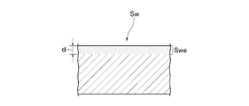
- the fragmentary sectional view of the sapphire substrate obtained by carrying out the present invention.
- IM is an ion implantation apparatus that can be used in the method for manufacturing the sapphire substrate Sw of the present embodiment.
- the ion implantation apparatus IM defines the plasma generation chamber 11a.
- a vacuum chamber 1 is provided in which a chamber 11 and a lower chamber 12 defining a plasma processing chamber 12a are connected in a vertical direction via an annular insulator 13.
- An exhaust pipe 21 from the vacuum pump 2 is connected to the lower chamber 12 so that the vacuum chamber 1 can be evacuated to a predetermined pressure.
- a quartz window 12b for high frequency introduction is provided on the ceiling wall of the upper chamber 11, and an antenna coil 5 for high frequency introduction connected to a high frequency power supply E1 having a known structure is provided above the quartz window 12b.
- the quartz window 12b is connected to a gas introduction pipe 3 leading to a gas source 31 containing nitrogen gas as a nitrogen-containing gas, and nitrogen gas is supplied at a predetermined flow rate by a mass flow controller 32 interposed in the gas introduction pipe 3. It can be introduced into the plasma generation chamber 11a. Then, after the vacuum chamber 1 is evacuated to a predetermined pressure, the mass flow controller 32 is controlled to introduce nitrogen gas into the plasma generation chamber 11a, and predetermined high frequency power is supplied to the coil 5 from the high frequency power supply E1.
- the plasma P can be generated in the plasma generation chamber 11a by ICP discharge.
- the plasma density can be changed by appropriately controlling the amount of nitrogen gas introduced and the input high frequency power, and the dose to the sapphire substrate Sw can be controlled.
- a grounded stage 4 for holding the sapphire substrate Sw so that one outer surface of the sapphire substrate Sw faces the plasma generation chamber 11a.
- the communicating portion 14 formed by the lower end opening of the upper chamber 11 and the upper end opening of the lower chamber 12 has a predetermined interval below the ion extraction electrode 6 formed of a mesh member and the ion extraction electrode 6.
- a mesh-like acceleration electrode 7 is provided, and the ion extraction electrode 6 and the acceleration electrode 7 are connected to an extraction / acceleration DC power source E2 having a known structure. Then, by controlling the DC power supply E2, it is possible to appropriately control the implantation energy of nitrogen ions into the sapphire substrate Sw.
- a method for manufacturing a sapphire substrate Sw having an antireflection function by injecting nitrogen ions from one side of the sapphire substrate W using the above-described ion implantation apparatus IM using a nitrogen-containing gas as a nitrogen gas will be specifically described.
- the vacuum chamber 1 is evacuated by the vacuum pump 2 with the sapphire substrate Sw placed on the stage 4 in the plasma processing chamber 12a.
- the mass flow controller 32 is controlled to introduce nitrogen gas into the plasma generation chamber 11a.
- the gas flow rate of nitrogen gas is controlled to a flow rate in the range of 1 to 50 sccm.
- a high frequency power of 0.1 kW or more is supplied from the high frequency power source E1 to the coil 5, and plasma P is generated in the plasma generation chamber 12a by ICP discharge.
- the DC power source E2 applies a voltage in the range of 0.2 kV to 3 kV between the upper chamber 11 and the ion extraction electrode 6, and a voltage in the range of 60 kV or less between the upper chamber 11 and the acceleration electrode 7, respectively.
- nitrogen molecular ions ionized mainly by the plasma P are extracted toward the plasma processing chamber 12a, accelerated, and injected into the sapphire substrate Sw with a predetermined implantation energy.
- the dose of nitrogen molecular ions is set in the range of 1E16 ions / cm 2 to 1E17 ions / cm 2 .
- the refractive index of the low refractive index region Swe cannot be lowered (for example, n ⁇ 1.8) to the extent that the antireflection function can be provided.
- the implantation energy of nitrogen molecular ions is set within a range of 60 keV or less.
- the implantation energy is higher than 60 keV, the low refractive index region becomes deep, and there is a problem that the high refractive index region exists on the surface side and the reflectance does not decrease (a good antireflection function cannot be imparted).
- visible light light having a wavelength in the range of 400 to 800 nm
- the low refractive index region Swe having a predetermined thickness d (for example, 20 nm ⁇ d ⁇ 150 nm) from the outer surface, which has a lower refractive index (n 1.3 to 1.7), is on the outer surface side of the sapphire substrate Sw. Formed.
- the reflectance for visible light having a specific wavelength in the range of 400 nm to 800 nm incident from the outer surface of the sapphire substrate Sw is smaller than the reflectance (about 8%) of the sapphire substrate.
- An antireflection function can be imparted to the substrate Sw.
- the following experiment was conducted using the ion implantation apparatus IM shown in FIG.
- a sapphire substrate Sw having a diameter of 50.8 mm and a thickness of 0.4 mm is used.
- the pressure in the plasma generation chamber 12a is in the order of 10 ⁇ 2 Pa
- the gas flow rate of nitrogen gas is 10 sccm
- the mass flow controller 32, the high frequency power supply E1, and the direct current power supply E2 were controlled so that the energy was 30 keV and the dose amount was 1E17 ions / cm 2 (at this time, the voltage between the upper chamber 11 and the ion extraction electrode 6 was 2 kV).
- the voltage between the upper chamber 11 and the acceleration electrode 7 is 30 kV). Then, when the reflectance on one surface of the sapphire substrate W into which nitrogen molecular ions were implanted was measured using a spectroscope (not shown), the reflectance for light having a wavelength in the range of 400 nm to 500 nm could be reduced to 1% or less, and 500 nm It was confirmed that the reflectance with respect to light having a wavelength in the range of ⁇ 800 nm could be 5% or less, and that the antireflection function could be imparted to the sapphire substrate Sw.
- FIG. 3 is a graph showing the reflectance with respect to the wavelength at that time. According to this, it was confirmed that if the implantation energy is changed, a specific wavelength region where the reflectance is desired to be reduced can be changed according to the application of the sapphire substrate Sw.
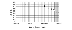
- FIG. 4 is a graph showing a change in refractive index with respect to the dose amount at that time. According to this, it was confirmed that when the dose amount is less than 5E15 ions / cm 2 , the refractive index of the low refractive index region cannot be lowered to the extent that an antireflection function can be provided.
- the ion implantation apparatus IM is an example of an apparatus that can be used in a method for manufacturing the sapphire substrate Sw.
- the plasma generation method is not limited to that using ICP discharge, and mass separation is performed.
- an ion implantation apparatus that implants only nitrogen gas ions into the sapphire substrate may be used.
- nitrogen gas as nitrogen-containing gas was demonstrated to the example, it is not limited to this, If it can inject
- IM ion implantation apparatus
- P plasma
- Sw sapphire substrate
- Swe low refractive index region
- 11a plasma generation chamber
Landscapes
- Chemical & Material Sciences (AREA)
- Metallurgy (AREA)
- Physics & Mathematics (AREA)
- Organic Chemistry (AREA)
- Engineering & Computer Science (AREA)
- Materials Engineering (AREA)
- Crystallography & Structural Chemistry (AREA)
- Inorganic Chemistry (AREA)
- Mechanical Engineering (AREA)
- Chemical Kinetics & Catalysis (AREA)
- Optics & Photonics (AREA)
- Electromagnetism (AREA)
- General Physics & Mathematics (AREA)
- Surface Treatment Of Optical Elements (AREA)
- Crystals, And After-Treatments Of Crystals (AREA)
Abstract
反射防止機能を持つサファイア基板を低コストで生産性よく製造することができるサファイア基板の製造方法を提供する。 サファイア基板Swの外表面側に、当該サファイア基板より屈折率の低い低屈折率領域を有して可視光に対する反射防止機能を持つ本発明のサファイア基板の製造方法は、サファイア基板の外表面に臨むプラズマ発生室11aに窒素含有ガスを導入し、プラズマPを発生させ、プラズマ中で電離した窒素イオンを加速してサファイア基板の外表面側から注入し、当該サファイア基板の外表面から所定厚さに亘る低屈折率領域Sweを形成する工程を含む。
Description
本発明は、サファイア基板の製造方法及びサファイア基板に関し、より詳しくは、サファイア基板の外表面側に、当該サファイア基板より屈折率の低い低屈折率領域を有して可視光に対する反射防止機能を持つサファイア基板の製造方法及びサファイア基板に関する。
近年、時計や携帯電話(スマートフォン)などの機器用の所謂カバーガラスに、無色透明で比較的高い硬度と強度を持つサファイア基板が用いられている。そして、機器の表示に対する利用者の視認性を高めるために、可視光(波長が400~800nmの範囲の光)に対する反射防止機能を持つようにサファイア基板の外表面に反射防止膜を積層することが知られている。
このような反射防止膜を備えたサファイア基板の製造方法は例えば特許文献1で知られている。このものでは、サファイア基板の表面に第1の窒化シリコン層、第1の酸化シリコン層、第2の窒化シリコン層及び最外層としての第2の酸化シリコン層を順次積層して反射防止膜が構成されている。この場合、各層は、反応性スパッタリング法により成膜される。
具体的には、スパッタリング装置の真空チャンバ内にシリコン製のターゲットとサファイア基板とを配置し、真空雰囲気下でアルゴン等の放電用ガスと共に窒素ガスまたは酸素ガスを適宜導入し、ターゲットに電力投入して真空チャンバ内にプラズマを形成し、プラズマ中の放電用ガスのイオンでシリコン製のターゲットをスパッタリングすることで反応性スパッタリング法により各層が形成される。然し、上記従来例のように反射防止膜を形成するのでは、所定膜厚の各層を順次形成していくのに時間がかかるばかりか、消耗品としてのターゲットを用いるため、製造コストが高くなるという問題がある。
本発明は、以上の点に鑑み、反射防止機能を持つサファイア基板を低コストで生産性よく製造することができるサファイア基板の製造方法及びサファイア基板を提供することをその課題とするものである。
上記課題を解決するために、サファイア基板の外表面側に、当該サファイア基板より屈折率の低い低屈折率領域を有して可視光に対する反射防止機能を持つ本発明のサファイア基板の製造方法は、サファイア基板の外表面に臨むプラズマ発生室に窒素含有ガスを導入し、プラズマを発生させ、プラズマ中で電離した窒素イオンを加速してサファイア基板の外表面側から注入し、当該サファイア基板の外表面から所定厚さに亘る低屈折率領域を形成する工程を含むことを特徴とする。
本発明によれば、サファイア基板の外表面側から窒素イオンを注入することで、サファイア基板の結晶内中に窒素イオンが存在し、サファイア基板(屈折率n=1.8)より低い屈折率(n=1.3~1.7の範囲)となる、外表面から所定厚さの低屈折率領域がサファイア基板の外表面側に形成される。そして、低屈折率領域の存在により、サファイア基板の外表面から入射する400nm~800nmの範囲の特定波長の可視光に対する反射率がサファイア基板の反射率(約8%)より小さくなり、サファイア基板に反射防止機能を付与することができる。この場合、所謂イオン注入法により窒素イオン(窒素原子、窒素分子のイオン)を注入するだけであるから、上記従来例の方法と比較して反射防止機能を付与するための時間を短縮できて生産性が向上し、しかも、ターゲット等が不要になることで製造コストも大幅に削減することができる。
本発明においては、窒素イオンを注入する工程にて窒素イオンのドーズ量を1E16ions/cm2~1E17ions/cm2の範囲に設定することが好ましい。これによれば、低屈折率領域の屈折率を確実にサファイア基板の屈折率より小さくできる。この場合、ドーズ量が1E16ions/cm2より少ないと、反射防止機能を付与できる程、低屈折率領域の屈折率を低下させる(例えば、n<1.8)ことができない。また、1E17ions/cm2より多くなると、イオン注入時間が長くなり過ぎ、実用的でない。
また、本発明においては、窒素イオンを注入する工程にて窒素イオンの注入エネルギーを60keV以下の範囲内で変化させることが好ましい。これによれば、サファイア基板の用途に応じて反射率を低下させたい特定の波長領域を変更することができ、有利である。この場合、注入エネルギーが60keVより大きいと、低屈折率領域が深くなり、その表面側に高屈折率領域が存在して反射率が低下しない(良好な反射防止機能を付与できない)という不具合がある。
上記課題を解決するために、サファイア基板の外表面側に、当該サファイア基板より屈折率の低い低屈折率領域を有して可視光に対する反射防止機能を持つ本発明のサファイア基板は、当該サファイア基板の外表面から所定厚さに亘る窒素イオンが注入された低屈折率領域を有することを特徴とする。
本発明においては、前記低屈折率領域の屈折率が、サファイア基板(屈折率n=1.8)よりも低い1.3~1.7であることが好ましい。
また、本発明においては、前記低屈折率領域に注入された窒素イオンのドーズ量は1E16ions/cm2~1E17ions/cm2の範囲内であることが好ましい。これによれば、低屈折率領域の屈折率を確実にサファイア基板の屈折率より小さくできる。
以下、図面を参照して、本発明のサファイア基板の製造方法の実施形態を説明する。図1を参照して、IMは、本実施形態のサファイア基板Swの製造方法に用いることができるイオン注入装置である。ここで、以下、「上」、「下」といった方向を示す用語を図1に示すイオン注入装置IMの姿勢を基準として説明すれば、イオン注入装置IMは、プラズマ発生室11aを画成する上チャンバ11と、プラズマ処理室12aを画成する下チャンバ12とを上下方向で環状の絶縁体13を介して連設してなる真空チャンバ1を備える。下チャンバ12には真空ポンプ2からの排気管21が接続され、真空チャンバ1を所定圧力に真空排気できるようになっている。
上チャンバ11の天井璧には高周波導入用の石英窓12bが設けられ、石英窓12bの上方には、公知の構造を持つ高周波電源E1に接続される高周波導入用のアンテナコイル5が設けられている。また、石英窓12bには、窒素含有ガスとしての窒素ガスを収納したガス源31に通じるガス導入管3が接続され、ガス導入管3に介設したマスフローコントローラ32により所定の流量で窒素ガスをプラズマ発生室11a内に導入できるようにしている。そして、真空チャンバ1内が所定圧力まで真空引きされた後、マスフローコントローラ32を制御してプラズマ発生室11a内に窒素ガスを導入し、高周波電源E1からコイル5に所定の高周波電力を投入することで、プラズマ発生室11a内にICP放電によりプラズマPを発生させることができる。この場合、窒素ガスの導入量及び投入高周波電力を適宜制御することでプラズマ密度を変化させることができ、サファイア基板Swへのドーズ量を制御することができる。
下チャンバ12内には、サファイア基板Swの一方の外表面がプラズマ発生室11aを臨むようにサファイア基板Swを保持するアース接地のステージ4が設けられている。また、上チャンバ11の下端開口と下チャンバ12の上端開口とで形成される連通部14には、メッシュ部材で構成されるイオン引出電極6と、イオン引出電極6の下方に所定間隔を存して配置されるメッシュ状の加速電極7とが設けられ、イオン引出電極6と加速電極7とが公知の構造を持つ引出・加速用の直流電源E2に接続されている。そして、直流電源E2を制御することでサファイア基板Swへの窒素イオンの注入エネルギーを適宜制御することができる。以下に、窒素含有ガスを窒素ガスとして、上記イオン注入装置IMを用いてサファイア基板Wの片面側から窒素イオンを注入して反射防止機能を持つサファイア基板Sw製造する方法を具体的に説明する。
先ず、プラズマ処理室12a内のステージ4上にサファイア基板Swを載置した状態で真空ポンプ2により真空チャンバ1内を真空排気する。真空チャンバ1内が所定圧力まで真空引きされると、マスフローコントローラ32を制御してプラズマ発生室11a内に窒素ガスを導入する。この場合、窒素ガスのガス流量を1~50sccmの範囲の流量に制御する。そして、高周波電源E1からコイル5に0.1kW以上の高周波電力を投入し、プラズマ発生室12a内にICP放電によりプラズマPを発生させる。
併せて、直流電源E2により、上チャンバ11とイオン引出電極6との間に0.2kV~3kVの範囲の電圧を、上チャンバ11と加速電極7との間に60kV以下の範囲の電圧を夫々印加することで、主としてプラズマPで電離した窒素分子イオンがプラズマ処理室12a側に向けて引き出され、加速されて所定の注入エネルギーでサファイア基板Swに注入される。この場合、窒素分子イオンのドーズ量は1E16ions/cm2~1E17ions/cm2の範囲に設定される。ドーズ量が1E16ions/cm2より少ないと、反射防止機能を付与できる程、低屈折率領域Sweの屈折率を低下させる(例えば、n<1.8)ことができない。また、1E17ions/cm2より多くなると、イオン注入時間が長くなり過ぎ、実用的でない。他方、窒素分子イオンの注入エネルギーは60keV以下の範囲内に設定される。注入エネルギーが60keVより大きくなると、低屈折率領域が深くなり、その表面側に高屈折率領域が存在して反射率が低下しない(良好な反射防止機能を付与できない)という不具合がある。尚、可視光(波長が400~800nmの範囲の光)においては注入エネルギーを15keV以上とすることで、より良好な反射防止機能を得られて有利である。
以上のようにしてサファイア基板Swの片面側から窒素イオンを注入すれば、図2に示すように、サファイア基板Swの結晶中に窒素イオンが存在し、サファイア基板(屈折率n=1.8)より低い屈折率(n=1.3~1.7の範囲)となる、外表面から所定厚さd(例えば、20nm<d<150nm)の低屈折率領域Sweがサファイア基板Swの外表面側に形成される。そして、低屈折率領域Sweの存在により、サファイア基板Swの外表面から入射する400nm~800nmの範囲の特定波長の可視光に対する反射率がサファイア基板の反射率(約8%)より小さくなり、サファイア基板Swに反射防止機能を付与することができる。
以上の実施形態によれば、所謂イオン注入法により窒素イオン(窒素原子、窒素分子のイオン)を注入するだけであるから、上記従来例の方法と比較して反射防止機能を付与するための時間を短縮できて生産性を向上でき、しかも、ターゲット等が不要になることで製造コストも大幅に削減することができる。
次に、本発明の効果を示すため図1に示すイオン注入装置IMを用いて次の実験を行った。サファイア基板Swとして、φ50.8mm×厚さ0.4mmのものを用い、また、窒素イオンの注入に際しては、プラズマ発生室12aの圧力が10-2Pa台、窒素ガスのガス流量が10sccm、注入エネルギーを30keV、ドーズ量が1E17ions/cm2になるように、マスフローコントローラ32、高周波電源E1及び直流電源E2を夫々制御した(このとき、上チャンバ11とイオン引出電極6との間の電圧は2kV、上チャンバ11と加速電極7との間の電圧は30kV)。そして、図外の分光器を用いて窒素分子イオンが注入されたサファイア基板Wの片面における反射率を測定したところ、400nm~500nmの範囲の波長の光に対する反射率を1%以下にでき、500nm~800nmの範囲の波長の光に対する反射率を5%以下にでき、サファイア基板Swに反射防止機能を付与できることが確認された。
次に、窒素分子イオンの注入に際して、直流電源E2を制御することで注入エネルギーのみを15keV、40keV、60keVに夫々変更してサファイア基板に窒素分子イオンを注入し、図外の分光器を用いて窒素分子イオンが注入されたサファイア基板Wの片面における反射率を測定した。図3は、そのときの波長に対する反射率を示すグラフである。これによれば、注入エネルギーを変更すれば、サファイア基板Swの用途に応じて反射率を低下させたい特定の波長領域を変更することができることが確認された。
次に、窒素分子イオンの注入に際して、ドーズ量のみを5E14ions/cm2~1E17ions/cm2の範囲で変更してサファイア基板に窒素分子イオンを注入し、図外の分光エリプソメータを用いて窒素分子イオンが注入された領域の屈折率を測定した。図4は、そのときのドーズ量に対する屈折率の変化を示すグラフである。これによれば、ドーズ量が5E15ions/cm2より少ないと、反射防止機能を付与できる程、低屈折率領域の屈折率を低下させることができないことが確認された。
以上、本発明の実施形態について説明したが、本発明は上記のものに限定されるものではない。即ち、上記イオン注入装置IMは、サファイア基板Swの製造方法に用いることができる一例の装置であり、例えばプラズマの発生方法はICP放電を利用したものに限られるものではなく、また、質量分離して窒素ガスイオンのみをサファイア基板に注入するようなイオン注入装置でもよい。また、上記実施形態では、窒素含有ガスとして窒素ガスを用いるものを例に説明したが、これに限定されるものではなく、窒素ガスイオンのみをサファイア基板に注入できるのであれば、広く適用することができる。
IM…イオン注入装置、P…プラズマ、Sw…サファイア基板、Swe…低屈折率領域、11a…プラズマ発生室。
Claims (6)
- サファイア基板の外表面側に、当該サファイア基板より屈折率の低い低屈折率領域を有して可視光に対する反射防止機能を持つサファイア基板の製造方法であって、
サファイア基板の外表面に臨むプラズマ発生室に窒素含有ガスを導入してプラズマを発生させ、プラズマ中で電離した窒素イオンを加速してサファイア基板の外表面側から注入し、当該サファイア基板の外表面から所定厚さに亘る低屈折率領域を形成する工程を含むことを特徴とするサファイア基板の製造方法。 - 前記窒素イオンを注入する工程にて窒素イオンのドーズ量を1E16ions/cm2~1E17ions/cm2の範囲に設定したことを特徴とする請求項1記載のサファイア基板の製造方法。
- 前記窒素イオンを注入する工程にて窒素イオンの注入エネルギーを60keV以下の範囲内で変化させることを特徴とする請求項1または請求項2記載のサファイア基板の製造方法。
- サファイア基板の外表面側に、当該サファイア基板より屈折率の低い低屈折率領域を有して可視光に対する反射防止機能を持つサファイア基板であって、
当該サファイア基板の外表面から所定厚さに亘る窒素イオンが注入された低屈折率領域を有することを特徴とするサファイア基板。 - 前記低屈折率領域の屈折率は1.3~1.7であることを特徴とする請求項4記載のサファイア基板。
- 前記低屈折率領域に注入された窒素イオンのドーズ量は1E16ions/cm2~1E17ions/cm2の範囲内であることを特徴とする請求項4または請求項5記載のサファイア基板
Priority Applications (1)
| Application Number | Priority Date | Filing Date | Title |
|---|---|---|---|
| JP2017555978A JPWO2017104443A1 (ja) | 2015-12-16 | 2016-12-02 | サファイア基板の製造方法及びサファイア基板 |
Applications Claiming Priority (2)
| Application Number | Priority Date | Filing Date | Title |
|---|---|---|---|
| JP2015-245501 | 2015-12-16 | ||
| JP2015245501 | 2015-12-16 |
Publications (1)
| Publication Number | Publication Date |
|---|---|
| WO2017104443A1 true WO2017104443A1 (ja) | 2017-06-22 |
Family
ID=59056346
Family Applications (1)
| Application Number | Title | Priority Date | Filing Date |
|---|---|---|---|
| PCT/JP2016/085880 Ceased WO2017104443A1 (ja) | 2015-12-16 | 2016-12-02 | サファイア基板の製造方法及びサファイア基板 |
Country Status (2)
| Country | Link |
|---|---|
| JP (1) | JPWO2017104443A1 (ja) |
| WO (1) | WO2017104443A1 (ja) |
Citations (9)
| Publication number | Priority date | Publication date | Assignee | Title |
|---|---|---|---|---|
| JPS48101947A (ja) * | 1972-04-08 | 1973-12-21 | ||
| JPH07113901A (ja) * | 1993-08-25 | 1995-05-02 | Fujitsu Ltd | 光学膜とその形成方法、反射防止膜とその形成方法、反射膜とその形成方法および光学膜を備えた光素子 |
| JPH11264901A (ja) * | 1997-12-10 | 1999-09-28 | Valtion Teknillinen Tutkimuskeskus | 光学的黒色表面およびその製造方法 |
| JP2003069007A (ja) * | 2001-08-24 | 2003-03-07 | Matsushita Electric Ind Co Ltd | 固体撮像装置およびその製造方法 |
| JP2009211078A (ja) * | 2009-04-10 | 2009-09-17 | Hitachi Ltd | 反射防止膜及びそれを有する画像表示装置,光記録媒体,太陽発電モジュール並びに反射防止膜形成方法 |
| JP2009271439A (ja) * | 2008-05-09 | 2009-11-19 | Mitsubishi Cable Ind Ltd | 反射防止膜を備えた光学部品 |
| WO2015081987A1 (en) * | 2013-12-03 | 2015-06-11 | Vertu Corporation Limited | Optical element with sapphire layer |
| JP2015121739A (ja) * | 2013-12-25 | 2015-07-02 | セイコーエプソン株式会社 | カバーガラスおよび時計 |
| WO2015176850A1 (en) * | 2014-05-23 | 2015-11-26 | Quertech | Single- and/or multi-charged gas ion beam treatment method for producing an anti-glare sapphire material |
-
2016
- 2016-12-02 JP JP2017555978A patent/JPWO2017104443A1/ja active Pending
- 2016-12-02 WO PCT/JP2016/085880 patent/WO2017104443A1/ja not_active Ceased
Patent Citations (9)
| Publication number | Priority date | Publication date | Assignee | Title |
|---|---|---|---|---|
| JPS48101947A (ja) * | 1972-04-08 | 1973-12-21 | ||
| JPH07113901A (ja) * | 1993-08-25 | 1995-05-02 | Fujitsu Ltd | 光学膜とその形成方法、反射防止膜とその形成方法、反射膜とその形成方法および光学膜を備えた光素子 |
| JPH11264901A (ja) * | 1997-12-10 | 1999-09-28 | Valtion Teknillinen Tutkimuskeskus | 光学的黒色表面およびその製造方法 |
| JP2003069007A (ja) * | 2001-08-24 | 2003-03-07 | Matsushita Electric Ind Co Ltd | 固体撮像装置およびその製造方法 |
| JP2009271439A (ja) * | 2008-05-09 | 2009-11-19 | Mitsubishi Cable Ind Ltd | 反射防止膜を備えた光学部品 |
| JP2009211078A (ja) * | 2009-04-10 | 2009-09-17 | Hitachi Ltd | 反射防止膜及びそれを有する画像表示装置,光記録媒体,太陽発電モジュール並びに反射防止膜形成方法 |
| WO2015081987A1 (en) * | 2013-12-03 | 2015-06-11 | Vertu Corporation Limited | Optical element with sapphire layer |
| JP2015121739A (ja) * | 2013-12-25 | 2015-07-02 | セイコーエプソン株式会社 | カバーガラスおよび時計 |
| WO2015176850A1 (en) * | 2014-05-23 | 2015-11-26 | Quertech | Single- and/or multi-charged gas ion beam treatment method for producing an anti-glare sapphire material |
Also Published As
| Publication number | Publication date |
|---|---|
| JPWO2017104443A1 (ja) | 2018-08-30 |
Similar Documents
| Publication | Publication Date | Title |
|---|---|---|
| US8889024B2 (en) | Plasma etching method | |
| EP2657363B1 (en) | Method of depositing silicon dioxide films | |
| WO2018052477A3 (en) | An integrated method for wafer outgassing reduction | |
| KR102258752B1 (ko) | 이산화규소의 증착 | |
| TW201043716A (en) | Ionized physical vapor deposition for microstructure controlled thin film deposition | |
| TW201248729A (en) | Silicon nitride film deposition method, organic electronic device manufacturing method, and silicon nitride film deposition device | |
| US20140199561A1 (en) | Coated article and method for manufacturing same | |
| CN101017793B (zh) | 一种扩散阻挡层的制作方法 | |
| JP2009068105A (ja) | 膜コーティングシステム及びその隔離装置 | |
| TWI912242B (zh) | 能夠時間性及/或空間性調變一或更多電漿的沉積工具 | |
| JP5909807B2 (ja) | プラズマ処理装置およびプラズマ処理方法 | |
| US20030033975A1 (en) | Method of forming a planar waveguide core | |
| JPWO2017104443A1 (ja) | サファイア基板の製造方法及びサファイア基板 | |
| CN103779203B (zh) | 等离子蚀刻方法 | |
| JP2016058643A (ja) | プラズマエッチング方法 | |
| WO2012158714A1 (en) | Ion-assisted direct growth of porous materials | |
| KR102177593B1 (ko) | 처리될 오브젝트의 표면에 이온을 주입하기 위한 방법 및 이 방법을 구현하기 위한 장치 | |
| US9698371B2 (en) | OLED device and preparation method thereof | |
| WO2010005070A1 (ja) | プラズマ処理装置およびプラズマ処理方法 | |
| KR101818623B1 (ko) | 알루미늄 산화질화물이 코팅된 투명기판 | |
| KR20170061764A (ko) | 스퍼터링 장치 | |
| JP5234773B2 (ja) | 酸化チタン膜の形成方法 | |
| CN101177781A (zh) | 在pecvd放电工艺中用于控制电磁辐射的系统和方法 | |
| CN107068917B (zh) | 成膜方法以及成膜装置 | |
| CN101177782A (zh) | 用于pecvd沉积工艺期间包覆屏蔽的系统和方法 |
Legal Events
| Date | Code | Title | Description |
|---|---|---|---|
| ENP | Entry into the national phase |
Ref document number: 2017555978 Country of ref document: JP Kind code of ref document: A |
|
| 121 | Ep: the epo has been informed by wipo that ep was designated in this application |
Ref document number: 16875426 Country of ref document: EP Kind code of ref document: A1 |
|
| NENP | Non-entry into the national phase |
Ref country code: DE |
|
| 122 | Ep: pct application non-entry in european phase |
Ref document number: 16875426 Country of ref document: EP Kind code of ref document: A1 |