WO2017094210A1 - 点火プラグ - Google Patents
点火プラグ Download PDFInfo
- Publication number
- WO2017094210A1 WO2017094210A1 PCT/JP2016/004152 JP2016004152W WO2017094210A1 WO 2017094210 A1 WO2017094210 A1 WO 2017094210A1 JP 2016004152 W JP2016004152 W JP 2016004152W WO 2017094210 A1 WO2017094210 A1 WO 2017094210A1
- Authority
- WO
- WIPO (PCT)
- Prior art keywords
- electrode
- tip
- electrode tip
- chip
- melting
- Prior art date
- Legal status (The legal status is an assumption and is not a legal conclusion. Google has not performed a legal analysis and makes no representation as to the accuracy of the status listed.)
- Ceased
Links
Images



Classifications
-
- H—ELECTRICITY
- H01—ELECTRIC ELEMENTS
- H01T—SPARK GAPS; OVERVOLTAGE ARRESTERS USING SPARK GAPS; SPARKING PLUGS; CORONA DEVICES; GENERATING IONS TO BE INTRODUCED INTO NON-ENCLOSED GASES
- H01T13/00—Sparking plugs
- H01T13/20—Sparking plugs characterised by features of the electrodes or insulation
- H01T13/32—Sparking plugs characterised by features of the electrodes or insulation characterised by features of the earthed electrode
-
- H—ELECTRICITY
- H01—ELECTRIC ELEMENTS
- H01T—SPARK GAPS; OVERVOLTAGE ARRESTERS USING SPARK GAPS; SPARKING PLUGS; CORONA DEVICES; GENERATING IONS TO BE INTRODUCED INTO NON-ENCLOSED GASES
- H01T13/00—Sparking plugs
- H01T13/20—Sparking plugs characterised by features of the electrodes or insulation
- H01T13/39—Selection of materials for electrodes
-
- H—ELECTRICITY
- H01—ELECTRIC ELEMENTS
- H01T—SPARK GAPS; OVERVOLTAGE ARRESTERS USING SPARK GAPS; SPARKING PLUGS; CORONA DEVICES; GENERATING IONS TO BE INTRODUCED INTO NON-ENCLOSED GASES
- H01T21/00—Apparatus or processes specially adapted for the manufacture or maintenance of spark gaps or sparking plugs
- H01T21/02—Apparatus or processes specially adapted for the manufacture or maintenance of spark gaps or sparking plugs of sparking plugs
Definitions
- This specification relates to a spark plug for igniting fuel gas in an internal combustion engine or the like.
- spark plugs have been used in internal combustion engines.
- the spark plug has a ground electrode that forms a gap.
- an electrode having an electrode tip made of a noble metal is used as the ground electrode.
- Patent Document 1 discloses a technique for welding an electrode tip to a tip holding portion and welding the tip holding portion to a ground electrode.
- This specification discloses a technique for suppressing the lifting and dropping of the electrode tip in a high temperature environment in a spark plug that fixes the electrode tip to the ground electrode using the tip holding part.
- a center electrode An electrode chip having a discharge surface that forms a gap with the central electrode, and an opposite surface opposite to the discharge surface, having a larger diameter than the discharge surface;
- a chip holding part having a through hole in which a part of the electrode chip is disposed;
- a ground electrode having a recess in which the tip holding portion and at least a part including the opposite surface of the electrode tip are disposed, one end being a connection end connected to the metal shell, and the other end being a free end
- the body A melted portion formed at least at a part of the boundary between the outer surface of the chip holding portion and the inner surface of the recess; With When the direction from the opposite surface toward the discharge surface is the first direction, the diameter of the end of the through hole in the first direction is not less than the diameter of the discharge surface and smaller than the diameter of the opposite surface,
- An ignition plug in which the electrode tip is held by an inner surface of the tip holding portion that forms the through hole and a bottom surface of the recess, On the surface on the first direction side
- the distance from the center of the first portion that intersects the first line to the center of the electrode tip in the melted portion is, of the melted portion, Longer than the distance from the center of the second part intersecting the second line to the center of the electrode tip, In a cross section passing through the first line and the axis of the electrode tip, The length in the first direction of the melted portion in the first portion is longer than the length in the first direction of the concave portion in the first portion, The length in the first direction of the melted part in the second part is longer than the length in the first direction of the concave part in the second part, In the first part, the melting part does not reach the electrode tip, The spark plug according to claim 2, wherein in the second portion, the melting part reaches the electrode tip.
- connection end side is less likely to reach a higher temperature than the free end side, even at the connection end side, cracks in the melted part due to thermal stress are unlikely to occur even if the melted part reaches the electrode tip.
- the length in the first direction of the melting portion is longer than the length in the first direction of the recess, so that the electrode tip is sufficiently Can be held with strength.
- the melting part does not reach the electrode tip, and in the second part, the melting part reaches the electrode tip, so that cracking occurs in the melting part while improving heat dissipation. Defects can be suppressed. Therefore, the electrode chip can be prevented from being lifted or dropped in a high temperature environment.
- the spark plug according to Application Example 1 is characterized in that the melting portion is formed over the entire circumference of the boundary between the outer surface of the chip holding portion and the inner surface of the recess.
- the strength for holding the electrode tip is improved, and therefore, lifting and dropping of the electrode tip can be more effectively suppressed in a high temperature environment.
- the spark plug according to Application Example 1 or 2 The electrode chip includes a chip body including the discharge surface, and a flange portion having a diameter larger than the diameter of the chip body, positioned on the opposite side of the first direction from the chip body, and including the opposite surface.
- the spark plug according to claim 2 wherein in the second portion, the melting portion reaches the flange portion of the electrode tip.
- the electrode tip since the electrode tip has the collar portion, the electrode tip can be securely held on the ground electrode body. Further, in the second portion, the melted part can surely reach the electrode tip. As a result, it is possible to more effectively suppress the lifting and dropping of the electrode tip in a high temperature environment.
- the present invention can be realized in various modes.
- an ignition plug and an ignition device using the ignition plug an internal combustion engine equipped with the ignition plug, and an ignition device using the ignition plug are provided.
- This can be realized in the form of an internal combustion engine or the like to be mounted.
- FIG. 1 It is sectional drawing of an example of the ignition plug of 1st Embodiment. It is a fragmentary sectional view which expands and shows the vicinity of the front-end
- FIG. 1 is a cross-sectional view of an example of a spark plug according to the first embodiment.
- the illustrated line CL indicates the axis CL of the spark plug 100.
- the illustrated cross section is a cross section including the axis CL.
- a direction parallel to the axis CL is also referred to as an “axis direction”.
- the lower direction in FIG. 1 is referred to as a front end direction LD, and the upper direction is also referred to as a rear end direction BD.
- the tip direction LD is a direction from the terminal fitting 40 described later toward the electrodes 20 and 30.
- the radial direction of the circle centered on the central axis is also simply referred to as “radial direction”, and the circumferential direction of the circle centered on the central axis is also referred to as “circumferential direction”.
- An end in the front end direction LD is also simply referred to as a front end, and an end in the rear end direction BD is also simply referred to as a rear end.
- the spark plug 100 includes an insulator 10, a center electrode 20, a ground electrode 30, a terminal fitting 40, a metal shell 50, a conductive first seal portion 60, a resistor 70, and a conductive second electrode.
- the seal portion 80, the first packing 8, the talc 9, the second packing 6, and the third packing 7 are provided.
- the insulator 10 is a substantially cylindrical member having a shaft hole 12 that is a through hole extending along the axis CL and penetrating the insulator 10.
- the insulator 10 is formed by firing alumina (other insulating materials can also be used).
- the insulator 10 includes a leg portion 13, a first reduced outer diameter portion 15, and a first trunk portion 17 that are arranged in order from the front end direction LD side (hereinafter also simply referred to as the front end side) toward the rear end direction BD. , A flange portion 19, a second reduced outer diameter portion 11, and a second body portion 18.
- the outer diameter of the first reduced outer diameter portion 15 gradually decreases from the rear end direction BD side (hereinafter simply referred to as the rear end side) toward the front end direction LD.
- the rear end side In the vicinity of the first reduced outer diameter portion 15 of the insulator 10 (the first body portion 17 in the example of FIG. 1), there is a reduced inner diameter portion 16 in which the inner diameter gradually decreases from the rear end side toward the front end direction LD. Is formed.
- the outer diameter of the second reduced outer diameter portion 11 gradually decreases from the front end side toward the rear end direction BD.
- a rod-like center electrode 20 extending along the axis CL is inserted on the tip side of the shaft hole 12 of the insulator 10.
- the center electrode 20 has a leg portion 25, a flange portion 24, and a head portion 23 that are arranged in order from the front end side toward the rear end direction BD.
- a portion on the distal end side of the leg portion 25 is exposed outside the shaft hole 12 on the distal end side of the insulator 10.
- the other part of the center electrode 20 is disposed in the shaft hole 12.
- the front end side surface of the flange portion 24 is supported by the reduced inner diameter portion 16 of the insulator 10.
- the center electrode 20 includes an electrode base material 21 and a core material 22 embedded in the electrode base material 21.
- the electrode base material 21 is formed using, for example, nickel (Ni) or an alloy containing nickel as a main component (for example, Inconel (“INCONEL” is a registered trademark)).
- the “main component” means a component having the highest content (hereinafter the same).
- As the content rate a value expressed in weight percent is adopted.
- the core material 22 is formed of a material (for example, an alloy containing copper) having a higher thermal conductivity than the electrode base material 21.
- a terminal fitting 40 is inserted on the rear end side of the shaft hole 12 of the insulator 10.
- the terminal fitting 40 is formed using a conductive material (for example, a metal such as low carbon steel).
- the terminal fitting 40 includes a cap mounting portion 41, a flange portion 42, and a leg portion 43 that are arranged in order from the rear end side toward the front end direction LD.
- the cap mounting portion 41 is exposed outside the shaft hole 12 on the rear end side of the insulator 10.
- the leg portion 43 is inserted into the shaft hole 12 of the insulator 10.
- a columnar resistor 70 for suppressing electrical noise is disposed between the terminal fitting 40 and the center electrode 20.
- a conductive first seal portion 60 is disposed between the resistor 70 and the center electrode 20, and a conductive second seal portion 80 is disposed between the resistor 70 and the terminal fitting 40. .
- the center electrode 20 and the terminal fitting 40 are electrically connected through the resistor 70 and the seal portions 60 and 80.
- the resistor 70 includes, for example, glass particles (for example, B 2 O 3 —SiO 2 glass) as main components, ceramic particles (for example, TiO 2 ), and a conductive material (for example, Mg). , Are used.
- the seal portions 60 and 80 are formed using, for example, glass particles similar to the resistor 70 and metal particles (for example, Cu).
- the metal shell 50 is a substantially cylindrical member having a through hole 59 that extends along the axis CL and penetrates the metal shell 50.
- the metal shell 50 is formed using a low carbon steel material (other conductive materials (for example, metal materials) can also be used).
- the insulator 10 is inserted into the through hole 59 of the metal shell 50.
- the metal shell 50 is fixed to the insulator 10 in a state of being disposed around the insulator 10 in the radial direction.
- the end portion on the distal end side of the insulator 10 (in this embodiment, the portion on the distal end side of the leg portion 13) is exposed outside the through hole 59.
- the end portion on the rear end side of the insulator 10 (in this embodiment, the portion on the rear end side of the second body portion 18) is exposed outside the through hole 59.
- the metal shell 50 includes a body portion 55, a seat portion 54, a deformation portion 58, a tool engagement portion 51, and a caulking portion 53 that are arranged in order from the front end side toward the rear end direction BD. ing.
- the seat part 54 is a bowl-shaped part.
- a screw portion 52 for screwing into a mounting hole of an internal combustion engine for example, a gasoline engine
- An annular gasket 5 formed by bending a metal plate is fitted between the seat portion 54 and the screw portion 52.
- the metal shell 50 has a reduced inner diameter portion 56 disposed on the tip side of the deformable portion 58.
- the inner diameter of the reduced inner diameter portion 56 gradually decreases from the rear end side toward the front end direction LD.
- the first packing 8 is sandwiched between the reduced inner diameter portion 56 of the metal shell 50 and the first reduced outer diameter portion 15 of the insulator 10.
- the first packing 8 is an iron O-ring (other materials (for example, metal materials such as copper) can also be used).
- the shape of the tool engaging portion 51 is a shape (for example, a hexagonal column) with which the spark plug wrench is engaged.
- a caulking portion 53 is provided on the rear end side of the tool engaging portion 51.
- the caulking portion 53 is disposed on the rear end side of the second reduced outer diameter portion 11 of the insulator 10 and forms an end on the rear end side of the metal shell 50.
- the caulking portion 53 is bent toward the inner side in the radial direction.
- an annular space SP is formed between the inner peripheral surface of the metal shell 50 and the outer peripheral surface of the insulator 10.
- the space SP is a space surrounded by the crimping portion 53 and the tool engagement portion 51 of the metal shell 50 and the second reduced outer diameter portion 11 and the second body portion 18 of the insulator 10. It is.
- a second packing 6 is disposed on the rear end side in the space SP.
- a third packing 7 is disposed on the front end side in the space SP. In this embodiment, these packings 6 and 7 are iron C-rings (other materials are also employable). Between the two packings 6 and 7 in the space SP, powder of talc (talc) 9 is filled.
- the crimping portion 53 is crimped so as to be bent inward. And the crimping part 53 is pressed to the front end side. Thereby, the deformation
- the first packing 8 is pressed between the first reduced outer diameter portion 15 and the reduced inner diameter portion 56 and seals between the metal shell 50 and the insulator 10. As a result, the gas in the combustion chamber of the internal combustion engine is prevented from leaking outside through the metal shell 50 and the insulator 10. In addition, the metal shell 50 is fixed to the insulator 10.
- the ground electrode 30 is joined to the end on the front end side of the metal shell 50.
- the ground electrode 30 includes an electrode body 33, an electrode tip 38, and a tip holding part 39.
- the electrode body 33 is a rod-shaped member.
- One end of the electrode body 33 is a connection end 332 that is connected to the end of the metal shell 50 on the front end side, for example, by resistance welding so as to be electrically connected.
- the other end of the electrode body 33 is a free end 333.
- the electrode body 33 extends from the connection end 332 connected to the metal shell 50 in the distal direction LD and is bent toward the axis CL.
- the electrode body 33 extends in a direction perpendicular to the axis line CL and reaches the free end 333.
- a portion of the electrode body 33 that extends in a direction perpendicular to the axis line CL is also referred to as a tip portion 331.
- An electrode tip 38 and a tip holder 39 are fixed on the rear end surface of the tip 331.
- the electrode tip 38 forms a gap (gap) g with the front end surface 20s1 (surface on the front end side) of the center electrode 20.
- the electrode main body 33 includes a base material 35 that forms the surface of the electrode main body 33, and a core portion 36 embedded in the base material 35.
- the base material 35 is formed using, for example, Ni or an alloy containing Ni as a main component (for example, Inconel).
- the core part 36 is formed using a material (for example, pure copper) whose thermal conductivity is higher than that of the base material 35.
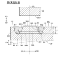
- FIG. 2 is an enlarged partial cross-sectional view showing the vicinity of the tip 331 of the ground electrode 30 of the first embodiment.
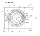
- FIG. 3 is a schematic view of the vicinity of the front end portion 331 of the ground electrode 30 as viewed from the rear end side toward the front end direction LD.
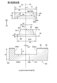
- FIG. 4 is an exploded view of the tip 331 of the ground electrode 30 before laser welding according to the first embodiment.
- the tip portion 331 described above extends in a direction perpendicular to the axis line CL.
- the direction perpendicular to the axis CL and directed from the axis CL toward the free end 333 is also referred to as a free end direction FD.
- a direction perpendicular to the axis CL and opposite to the free end direction FD, that is, a direction from the axis CL toward the connection end 332 is also referred to as a connection end direction CD.
- the electrode tip 38 has a discharge surface 38s1 on the rear end side and an opposite surface 38s2 on the side opposite to the discharge surface 38s1 (that is, on the front end side).
- the discharge surface 38s1 is a surface that forms a gap g between the front surface 20s1 of the center electrode 20 and the discharge surface 38s1.
- the electrode tip 38 includes a tip body 381 including a discharge surface 38s1 and a flange portion 382 including an opposite surface 38s2 and positioned on the tip side from the tip body 381.
- the outer diameter of the chip body 381 is linearly reduced toward the center electrode 20, that is, from the front end side to the rear end side.
- the chip body 381 has a truncated cone shape having a so-called tapered outer surface 381s.
- the outer diameter of the flange 382 is larger than the diameters of the tip and rear ends of the chip body 381.
- the axis CL of the electrode tip is the same as the axis CL of the spark plug 100.
- the diameter R2 (FIG. 4) of the opposite surface 38s2 is larger than the diameter R1 (FIG. 4) of the discharge surface 38s1.
- the electrode tip 38 is formed by using an alloy containing a noble metal having excellent spark consumption as a main component.
- the noble metal as the main component is iridium.
- Ir has a high melting point among noble metals and is excellent in spark wear resistance. Therefore, it is preferable to form the electrode tip 38 using Ir or an alloy containing Ir as a main component.
- the chip holding part 39 has a cylindrical outer shape.
- a through hole 395 is formed in the chip holding part 39.
- the axis line CL of the through hole 395 is the same as the axis line CL of the spark plug 100.
- the axis CL of the through hole 395 and the axis Co of the cylindrical outer shape of the chip holding part 39 are parallel to each other.
- the axis line Co of the cylindrical outer shape of the chip holding part 39 is shifted in the free end direction FD with respect to the axis line CL of the through hole 395. Therefore, as shown in FIG.
- the distance Lf (FIG. 4) is longer than the distance Lc between the portion of the outer surface 391 of the chip holding portion 39 located in the connection end direction CD as viewed from the axis CL and the axis CL.
- the through-hole 395 includes a rear end side hole 395a and a front end side hole 395b which is located on the front end side of the rear end side hole 395a and has a diameter larger than the diameter of the rear end side hole 395a.
- the shape of the hole 395a on the rear end side corresponds to the shape of a part on the front end side of the tip body 381 of the electrode tip 38, and the diameter is linearly reduced from the front end side toward the rear end side.
- the shape of the hole 395 b on the distal end side corresponds to the shape of the flange portion 382 of the electrode tip 38 and has a diameter substantially equal to the outer shape of the flange portion 382.
- a step 395c is formed between the hole 395a on the rear end side and the hole 395b on the front end side.
- the diameter R3 (FIG. 4) at the rear end of the through hole 395 is equal to or larger than the diameter R1 (FIG. 4) of the discharge surface 38s1 and smaller than the diameter R2 of the opposite surface 38s2.
- a concave portion 335 that is recessed toward the distal end direction LD is formed at a position facing the distal end surface 20 s 1 of the center electrode 20 on the surface of the electrode body 33.
- maintenance part 39 is welded is a substantially cylindrical shape.
- the substantially cylindrical axis Co of the recess 335 is the same as the cylindrical outer axis Co of the chip holding part 39.
- the recess 335 is formed in the base material 35 of the electrode body 33.
- the concave portion 335 before the tip holding portion 39 is welded has an inner side surface 335s1 and a bottom surface 335s2. Inside the recess 335, a part of the tip side including the opposite surface 38 s 2 of the electrode tip 38 and a tip holding portion 39 surrounding the electrode tip 38 are disposed.
- a melting portion 82 is formed over the entire circumference at the boundary between the outer surface of the chip holding portion 39 and the inner surface of the recess 335.
- the hatched portion is a portion of the melted portion 82 exposed at the surface 33 s on the rear end side of the electrode body 33.
- the melting part 82 is formed by irradiating a laser in a direction perpendicular to the surface 33s.
- the length (depth) L1 (FIG. 2) in the axial direction of the melting portion 82 is longer than the length L2 in the axial direction of the chip holding portion 39 on the entire circumference. Further, the length L1 (FIG.
- the electrode tip 38 is formed in the electrode body 33 by the inner surface of the tip holding part 39 that forms the through hole 395 and the bottom face 335 s 2 of the recess 335. Is retained.
- a virtual line extending in the free end direction FD from the axis CL of the electrode tip 38 is defined as a first line VL1, and the connection end from the axis CL of the electrode tip 38 is connected.
- a virtual line going up in the direction CD is defined as a second line VL2.
- a distance Df from the center CP1 of the first portion PT1 to the center of the electrode tip 38 is longer than a distance Dc from the center CP2 of the second portion PT2 to the center of the electrode tip 38.
- the axis Co of the cylindrical outer shape of the chip holding portion 39 is displaced in the free end direction FD with respect to the axis CL of the through hole 395, as shown in FIG.
- the distance Lf between the portion positioned in the free end direction FD when viewed from the axis CL and the axis CL is the tip holding portion before welding. This is because the outer side surface 391 of 39 is longer than the distance Lc between the portion located in the connecting end direction CD as viewed from the axis CL and the axis CL.
- FIG. 2 can be said to be a sectional view in which the ground electrode 30 and the center electrode 20 are cut along a plane including the axis line CL of the electrode tip 38, the first line VL1, and the second line VL2. it can.
- the above-described cross section of the first portion PT1 and the cross section of the second portion PT2 of the melting part 82 appear.
- the melting portion 82 does not reach the electrode tip 38 in the first portion PT1. That is, as indicated by a circle C1, the melting portion 82 and the electrode tip 38 are separated from each other in the first portion PT1.
- FIG. 1 the melting portion 82 and the electrode tip 38 are separated from each other in the first portion PT1.
- the melting portion 82 reaches the electrode tip 38 (specifically, the flange portion 382 of the electrode tip 38). That is, as shown by a circle C2, in the second portion PT2, a part of the flange portion 19 of the electrode tip 38 is melted by laser welding to become a part of the melting portion 82. For this reason, as shown by a circle C2, in the second portion PT2, the flange portion 382 of the electrode tip 38 and the melting portion 82 are in contact with each other.
- the length L1 (FIG. 2) in the axial direction of the melting portion 82 is longer than the length L3 in the axial direction of the recess 335 on the entire circumference. Accordingly, in both the first part PT1 and the second part PT2, the length L1 in the axial direction of the melting portion 82 is longer than the length L3 in the axial direction of the recess 335.
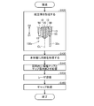
- FIG. 5 is a flowchart showing an example of a method for manufacturing a spark plug.
- step S120 an assembly is formed. The assembly is in a state before the bending of the electrode body 33 of the ground electrode 30 and the attachment of the electrode tip 38 and the tip holding portion 39 onto the electrode body 33 in the manufacturing process of the spark plug 100 shown in FIG. belongs to.
- step S120 in FIG. 5 a partial cross-sectional view showing the vicinity of the center electrode 20 of the assembly 100x is shown.
- the assembly 100 x includes an insulator 10, a metal shell 50 fixed to the insulator 10, and a center electrode 20 inserted into the shaft hole 12 of the insulator 10.
- a linear electrode body 33x is joined to the metal shell 50 as the electrode body 33 before being bent.
- the base material 35 and the core portion 36 of the electrode body 33x are not shown.
- the base material 35 and the core part 36 may be omitted.
- various known methods can be adopted, and detailed description thereof is omitted.
- a recess 335 is formed in the electrode body 33x of the ground electrode 30.
- the shape of the recess 335 is as described with reference to FIG.
- the recess 335 is formed in the electrode main body 33x before being bent using, for example, a cutting tool such as a drill.
- step S140 the electrode tip 38 and the tip holding portion 39 are disposed in the formed recess 335.
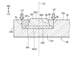
- FIG. 6 is a view showing a state in which the electrode tip 38 and the tip holding portion 39 are arranged in the recess 335. Specifically, the electrode tip 38 is disposed in the through hole 395 of the tip holding portion 39. Then, the chip holding part 39 and the electrode chip 38 in this state are fitted into the recess 335.
- step S150 the chip holder 39 is laser welded into the recess 335.
- An arrow LZ in FIG. 6 conceptually shows laser irradiation for laser welding.
- the laser LZ is irradiated perpendicularly to the surface 33 s of the electrode body 33 on the boundary BL between the inner side surface 335 s 1 of the recess 335 and the outer side surface 391 of the chip holding unit 39.
- the laser LZ irradiation is performed over the entire circumference of the boundary BL between the inner surface 335 s 1 of the recess 335 and the outer surface 391 of the chip holding unit 39.
- the laser LZ is irradiated at 24 places at a speed of 12 Hz, so that the melting portion 82 is formed over the entire circumference of the boundary BL.
- the melting part 82 of FIGS. 2 and 3 is formed.
- the melting part 82 is a part including the components of the electrode body 33 (base material 35) and the components of the chip holding part 39, which are melted together.
- the electrode main body 33 and the tip holding part 39 are joined via a melting part 82. Therefore, the melting part 82 can also be referred to as a joining part that joins the electrode body 33 and the chip holding part 39, and can also be called a bead that joins the electrode body 33 and the chip holding part 39.
- the melting part 82 is formed by being melted at a high temperature.
- the fine structure such as the particle size is different from the chip holding portion 39.
- step S160 the electrode body 33x is bent to form a gap g. That is, as shown in FIG. 2, the electrode body 33 x is bent toward the center electrode 20 so that the tip surface 20 s 1 of the center electrode 20 and the discharge surface 38 s 1 of the electrode tip 38 face each other.
- the amount of deviation of the axis Co of the chip holding portion 39 from the axis CL of the electrode tip 38 in the free end direction FD is defined as an offset amount OF (FIGS. 3 and 4).
- the offset amount OF is different and is 0, 0.1 mm, 0.2 mm, 0.3 mm, and 0.4 mm. Since the offset amount OF is 0, the sample 1 is not a sample of the spark plug 100 of the embodiment but a sample for comparison.
- the electrode tip 38 was formed using an iridium alloy, and the electrode body 33 and the tip holding portion 39 were formed using Inconel 600, which is a nickel alloy.
- the melting part 82 reaches the collar part 382 of the electrode tip 38 in both the first part PT1 and the second part PT2 described above. Further, in the samples 2 to 5 of the spark plug 100 of the embodiment, the melting portion 82 does not reach the flange portion 382 of the electrode tip 38 in the first portion PT1, and the melting portion 82 is not reached in the second portion PT2. , And reaches the collar portion 382 of the electrode tip 38.
- the appearance of the melting part 82 of samples 1 to 5 was evaluated.
- An evaluation of a sample in which the melting part 82 does not show adhesion (so-called rising of melting dripping) to the side surface of the electrode tip 38 is “A”, and evaluation of a sample in which adhesion to the side surface of the electrode tip 38 is slightly seen
- the evaluation of the sample in which the adhesion to the side surface of the electrode tip 38 clearly occurred was “C”.
- a cooling test was performed on samples 1 to 5.
- the cycle of heating and cooling was repeated 1000 times in the vicinity of the electrode tip 38 of the ground electrode 30 of each sample.
- a high-frequency heater was used to heat at 950 to 100 degrees Celsius for 2 minutes for 2 minutes, and then naturally cooled in air for 1 minute.
- chip bondability was evaluated. Specifically, it was confirmed whether the electrode tip 38 was lifted or dropped. The confirmation was performed by comparing the result of tracing the external shape of the electrode tip 38 as viewed from the direction perpendicular to the axial direction with the eye before and after the test. The evaluation of the sample in which the electrode tip 38 was not lifted or dropped off was “A”, and the evaluation of the sample in which the electrode tip 38 was lifted or dropped was “C”.
- thermal conductivity was evaluated. Specifically, the amount of decrease ⁇ T in temperature of the electrode tip 38 due to cooling for 1 minute after the end of heating for 2 minutes in the cooling test was measured using a thermocouple. Then, the evaluation of the sample whose average value of the decrease amount ⁇ T is 100 degrees or more is “A”, and the evaluation of the sample whose average value of the decrease amount ⁇ T is 50 degrees or more and less than 100 degrees is “B”. The evaluation of the sample whose average value of the amount ⁇ T is less than 50 degrees is “C”.
- the deformation of the ground electrode 30 was evaluated. Specifically, the amount of deformation ⁇ H in which the free end 333 of the electrode body 33 is deformed after the test in the direction indicated by the arrow AR in FIG. 2 (that is, the tip direction LD along the axis CL of the electrode tip 38) is measured. did.
- the evaluation of the sample with the deformation amount ⁇ H of 0 is “A”
- the evaluation of the sample with the deformation amount ⁇ H of less than 1 mm is “B”
- the evaluation of the sample with the deformation amount ⁇ H of 1 mm or more is “C”.
- the evaluation of Samples 1 and 2 whose offset amounts OF are 0 and 0.1 mm is “A”, and Samples 3 and 4 whose offset amounts OF are 0.2 mm and 0.3 mm.
- the evaluation of “5” was “B”, and the evaluation of Sample 5 in which the offset amount OF was 0.4 mm was “C”.
- the offset amount OF increases, the distance between the outer surface 391 of the chip holding portion 39 and the outer surface 381s of the electrode tip 38 becomes closer on the connection end direction CD side. Get closer. For this reason, it is considered that the melting part 82 is easily attached to the electrode tip 38.
- the evaluation of the sample 1 in which the offset amount OF is 0 is “C”
- the evaluation of the samples 2 to 5 in which the offset amount OF is 0.1 mm to 0.4 mm is “A” "Met.
- the reason for this is as follows.
- the temperature on the connection end direction CD side is lowered by heat pulling, but the temperature on the free end direction FD side is not easily lowered because there is no heat pulling.
- the temperature on the free end direction FD side of the ground electrode 30 is higher than the temperature on the connection end direction CD side.
- the electrode tip 38 and the tip holding portion 39 are made of different materials, they have different thermal expansion coefficients.
- the thermal expansion coefficient of the nickel alloy tip holding portion 39 is larger than the thermal expansion coefficient of the noble metal electrode tip 38. For this reason, if the melting portion 82 reaches the electrode tip 38 in the first portion PT1 on the free end direction FD side that becomes high temperature, a relatively large thermal stress is generated in this portion. As a result, cracks are likely to occur in the melted portion 82 due to thermal stress. As a result, the electrode tip 38 is likely to be lifted or dropped at the first portion PT1 on the free end direction FD side. As described above, in Sample 1 in which the offset amount OF is 0, the melting portion 82 reaches the electrode tip 38 in the first portion PT1 on the higher-temperature free end direction FD side, so that the electrode tip 38 is lifted.
- the evaluation of the sample 1 in which the offset amount OF is 0 is “C” similarly to the evaluation of the chip bondability, and the offset amount OF is 0.1 mm to 0.4 mm.
- the evaluation of Samples 2 to 5 was “A”. The reason for this is as follows. As described above, when the melting portion 82 reaches the electrode tip 38 in the first portion PT1 on the free end direction FD side where the temperature is higher, a relatively large thermal stress is generated. It is considered that the electrode body 33 is deformed due to the thermal stress. As described above, in the sample 1 in which the offset amount OF is 0, the melting portion 82 reaches the electrode tip 38 in the first portion PT1 on the higher temperature free end direction FD side. Is likely to occur.
- the offset amount OF is provided, and the melting portion 82 does not reach the electrode tip 38 in the first part PT1, It has been found that the melted portion 82 preferably reaches the electrode tip 38 in the two-part PT2. From the viewpoint of the appearance of the melting portion 82, it is not preferable that the offset amount OF is excessively large. Overall, it was found that the offset amount OF is preferably 0.1 mm or more and 0.3 mm or less.
- the free end 333 side of the ground electrode 30 is likely to become hot. Because it is a free end, it can not be expected to heat. Further, if the melting portion 82 reaches the electrode tip 38 on the free end 333 side of the ground electrode 30, the free end 333 side tends to become high temperature, so that the heat between the electrode tip 38 and the tip holding portion 39 can be increased. Cracks are likely to occur in the melted portion 82 due to thermal stress based on the difference in expansion coefficient. On the other hand, on the connection end 332 side of the ground electrode 30, if the melting part 82 reaches the electrode tip 38, heat extraction is improved.
- connection end 332 side is less likely to reach a higher temperature than the free end 333 side, even if the melting portion 82 reaches the electrode tip 38 on the connection end 332 side, cracks in the melting portion 82 due to thermal stress. Is unlikely to occur. Therefore, according to the spark plug 100 of the above-described embodiment, the axial length L1 of the melting portion 82 is the recess 335 in the first portion PT1 on the free end 333 side and the second portion PT2 on the connection end 332 side. Therefore, the electrode tip 38 can be held with sufficient strength.
- the melting part 82 does not reach the electrode tip 38, and in the second part PT2, the melting part 82 reaches the electrode tip 38, so that the heat extraction is improved and the melting is performed.
- the trouble that a crack occurs in the portion 82 can be suppressed. Therefore, the electrode chip can be prevented from being lifted or dropped in a high temperature environment.
- the melting part 82 is formed over the entire circumference of the boundary between the outer side surface of the chip holding part 39 and the inner side surface of the recess 335. As a result, it is possible to more effectively suppress the lifting and dropping of the electrode tip in a high temperature environment.
- the electrode tip 38 has a tip body 381 and a flange portion 382.
- the melting portion 82 reaches the flange portion 382 of the electrode tip 38.
- the electrode tip 38 can be reliably held on the electrode body 33.
- the melting portion 82 can be reliably reached the electrode tip. As a result, the lifting and dropping of the electrode tip 38 can be more effectively suppressed in a high temperature environment.
- the axis Co of the tip holding portion 39 is shifted in the free end direction FD with respect to the axis CL of the electrode tip 38.
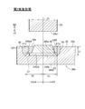
- FIG. 7 is an enlarged partial sectional view showing the vicinity of the tip 331b of the ground electrode 30b of the second embodiment.
- FIG. 8 is an exploded view of the tip 331b of the ground electrode 30b before laser welding according to the second embodiment.
- the shape of the chip holding part 39b is different from that of the chip holding part 39 of the first embodiment.
- the shape of the recessed part 335b formed in the electrode main body 33b differs from the recessed part 335 of 1st Embodiment.
- the electrode tip 38 of the second embodiment is the same as the electrode tip 38 of the first embodiment.
- the chip holding part 39b of the second embodiment has a cylindrical outer shape.
- the chip holding part 39b of the second embodiment has a hole 395a on the rear end side of the chip holding part 39 (FIG. 4) of the first embodiment as a through hole.
- maintenance part 39b of 2nd Embodiment does not have the hole 395b of the front end side of the chip
- the axial length L2b of the chip holding part 39b of the second embodiment is shorter than the axial length L2 of the chip holding part 39 of the first embodiment.
- the concave portion 335b of the second embodiment is positioned on the rear end side from the front end side portion 335b1 and has a larger diameter than the front end side portion 335b1. And a rear end side portion 335b2.
- the rear end portion 335b2 has a substantially cylindrical shape into which the chip holding portion 39b is fitted.
- the axis line CL of the tip end portion 335b1 is the same as the axis line CL of the electrode tip 38 and the axis line CL of the through hole 395a of the tip holding portion 39b.
- the axis Co of the rear end side portion 335b2 is the same as the axis Co of the cylindrical outer shape of the chip holding portion 39b.
- the axis Co of the rear end side portion 335b2 is shifted in the free end direction FD with respect to the axis CL of the front end side portion 335b1.
- the length L3b2 in the axial direction of the rear end portion 335b2 is equal to the length L2b in the axial direction of the chip holding portion 39b.
- the length L3b1 in the axial direction of the tip end portion 335b1 is equal to the length L5 in the axial direction of the flange portion 382 of the electrode tip 38.
- the tip holding portion 39b being laser welded to the electrode body 33b, the inner surface of the tip holding portion 39b forming the through hole 395a and the bottom surface 335b4 of the recess 335b (ie, the tip)
- the electrode tip 38 is held in the electrode body 33b by the bottom surface of the side portion 335b1.
- the chip holding portion 39b is supported by a step portion 335b3 formed between the front end side portion 335b1 and the rear end side portion 335b2.
- the distance Df from the center CP1 of the first portion PT1 on the free end direction FD side to the center of the electrode tip 38 is the connection end direction. It is longer than the distance Dc from the center CP2 of the second portion PT2 on the CD side to the center of the electrode tip 38.
- melting part 82 is longer than the length L3 (L3b1 + L3b2) of the axial direction of the recessed part 335 in the perimeter.
- the melting portion 82 does not reach the electrode tip 38 in the first portion PT1.
- the melted portion 82 reaches the electrode tip 38 (specifically, the flange portion 382 of the electrode tip 38) in the second portion PT ⁇ b> 2.
- the melting part 82 does not reach the electrode tip 38, and in the second part PT2, the melting part 82 reaches the electrode tip 38.
- the electrode chip can be prevented from being lifted or dropped in a high temperature environment.
- the melting portion 82 is formed over the entire circumference of the boundary between the outer surface of the chip holding portion 39 and the inner surface of the recess 335.
- the melting portion is not limited to this, and may be formed at a part of the boundary with the inner surface of the recess 335.
- FIG. 9 is an explanatory diagram of a ground electrode 30c according to a modification. 9, the outline of the vicinity of the front end portion 331c of the ground electrode 30c viewed from the rear end side toward the front end direction LD is shown, as in FIG.
- the melting part includes a first melting part 82c1 located on the free end direction FD side and a second melting part 82c2 located on the connection end direction CD side.
- the configuration other than the melting portion of the ground electrode 30c in FIG. 9 is the same as that in the first embodiment.
- the first melting part 82c1 includes a first part PT1 that intersects with the above-described first line VL1
- the second melting part 82c2 includes a second part PT2 that intersects with the above-described second line VL2.
- no melting part is formed in the direction perpendicular to the first line VL1 and the second line VL2 as seen from the axis CL of the electrode tip 38.
- the second melting portion 82c2 reaches the electrode tip 38 within the range of the angle ⁇ in the circumferential direction around the second portion PT2 of the second melting portion 82c2. Outside the range of the angle ⁇ in the circumferential direction, the second melting portion 82c2 does not reach the electrode tip 38.
- the angle ⁇ indicating the range of the melted portion reaching the electrode tip 38 is preferably less than 160 degrees, and more preferably 30 degrees or more and less than 120 degrees.
- the shape of the electrode tip 38 and the shape of the tip holding portions 39 and 39b are not limited to the shapes described in the above embodiments, and various other shapes can be employed.
- the electrode chip may be configured to include only the chip body 381 without including the flange portion 382.
- the outer shape of the electrode tip may be reduced stepwise from the front end direction LD toward the rear end direction BD.
- the shape of the chip holding portion 39 viewed from the rear end side toward the front end direction LD may not be a circle but may be another shape.
- the shape of the chip holding portion 39 viewed from the rear end side toward the front end direction LD may be an ellipse in which the length in the free end direction FD is longer than the length in the direction orthogonal to the free end direction FD.
- maintenance part 39 is formed using Inconel 600, you may form using another heat-resistant material, for example, a heat-resistant nickel alloy different from Inconel 600.
- the melting portion extends in a direction orthogonal to the surface 33 s of the electrode body 33. That is, in the laser welding of each of the above embodiments, the laser is irradiated in a direction orthogonal to the surface 33 s of the electrode body 33.
- the melting part may extend obliquely with respect to the surface 33 s of the electrode body 33.
- the melting portion may be inclined obliquely so that the position farther from the surface 33 s of the electrode body 33 (that is, the deeper the position) is, the closer to the axis CL of the electrode tip 38.
- the melting part may be inclined obliquely so as to be away from the axis CL of the electrode tip 38 as the position is farther from the surface 33 s of the electrode body 33 (that is, as the position is deeper).
- the electrode tip 38 of the above embodiment is formed of an iridium alloy, but may be formed of a noble metal different from iridium or an alloy containing the noble metal as a main component.
- a noble metal different from iridium for example, platinum (Pt) or rhodium (Rh) may be employed.
- the configuration of the spark plug is not limited to the configuration described in FIG. 1, and various configurations can be employed.
- an electrode tip may be provided in a portion of the center electrode 20 where the gap g is formed.
- an alloy containing a noble metal such as iridium or platinum can be used.
- the core material 22 of the center electrode 20 may be omitted.
Landscapes
- Spark Plugs (AREA)
Abstract
電極チップの浮き上がりや脱落を抑制する。点火プラグは、中心電極と、放電面と、放電面より大きな径を有し、放電面とは反対側の反対面と、を有する電極チップと、貫通孔を有するチップ保持部と、凹部を有する接地電極本体と、チップ保持部の外側面と、凹部の内側面と、の境界の少なくとも一部に形成された溶融部と、を備える。電極チップの軸線から接地電極の自由端に向かう方向に延びる仮想線を第1の線とし、電極チップの軸線から接地電極の接続端に向かう方向に延びる仮想線を第2の線とする。溶融部のうち、第1の線と交差する第1部分の中心から電極チップの中心までの距離は、溶融部のうち、第2の線と交差する第2部分の中心から電極チップの中心までの距離より長く、第1部分において、溶融部は、電極チップに到達せず、第2部分において、溶融部は、電極チップに到達している。
Description
本明細書は、内燃機関等において燃料ガスに点火するための点火プラグに関する。
従来から、内燃機関に、点火プラグが用いられている。点火プラグは、間隙(ギャップ)を形成する接地電極を有している。接地電極には、例えば、貴金属で形成された電極チップを有する電極が利用されている。特許文献1では、電極チップをチップ保持部に溶接し、チップ保持部を接地電極に溶接する技術が開示されている。
しかしながら、上記の技術では、接地電極とチップ保持部との間の溶接や、チップ保持部と電極チップとの間の溶接について、十分に工夫がされているとは言えなかった。このために、点火プラグの使用時に、点火プラグの接地電極近傍が高温環境下に曝された場合に、これらの溶接部にクラックが発生する不具合を十分に抑制することができない可能性があった。この結果、例えば、高温環境下にて、電極チップの浮き上がりや、脱落を引き起こす可能性があった。
本明細書は、チップ保持部を用いて電極チップを接地電極に固定する点火プラグにおいて、高温環境下にて、電極チップの浮き上がりや脱落を抑制する技術を開示する。
本明細書に開示される技術は、以下の適用例として実現することが可能である。
[適用例1]中心電極と、
前記中心電極との間に間隙を形成する放電面と、前記放電面より大きな径を有し、前記放電面とは反対側の反対面と、を有する電極チップと、
前記電極チップのうちの一部が内部に配置される貫通孔を有するチップ保持部と、
前記チップ保持部と前記電極チップのうちの前記反対面を含む少なくとも一部分とが配置される凹部を有し、一端が主体金具に接続される接続端であり、他端が自由端である接地電極本体と、
前記チップ保持部の外側面と、前記凹部の内側面と、の境界の少なくとも一部に形成された溶融部と、
を備え、
前記反対面から前記放電面に向かう方向を第1方向とするとき、前記貫通孔の前記第1方向の端の径は、前記放電面の径以上、かつ、前記反対面の径より小さく、
前記貫通孔を形成する前記チップ保持部の内面と、前記凹部の底面と、によって前記電極チップが保持される点火プラグであって、
前記接地電極本体の前記第1方向側の面において、前記電極チップの軸線から前記自由端に向かう方向に延びる仮想線を第1の線とし、前記電極チップの軸線から前記接続端に向かう方向に延びる仮想線を第2の線とするとき、
前記接地電極本体の前記第1方向側の面において、前記溶融部のうち、前記第1の線と交差する第1部分の中心から前記電極チップの中心までの距離は、前記溶融部のうち、前記第2の線と交差する第2部分の中心から前記電極チップの中心までの距離より長く、
前記第1の線と前記電極チップの軸線とを通る断面において、
前記第1部分における前記溶融部の前記第1方向の長さは、前記第1部分における前記凹部の前記第1方向の長さより長く、
前記第2部分における前記溶融部の前記第1方向の長さは、前記第2部分における前記凹部の前記第1方向の長さより長く、
前記第1部分において、前記溶融部は、前記電極チップに到達せず、
前記第2部分において、前記溶融部は、前記電極チップに到達していることを特徴とする、点火プラグ。
溶融部が接地電極の自由端側で、電極チップに到達していても、接地電極の自由端側は、高温になりやすい上に、自由端であるために、熱引きが期待できない。また、溶融部が接地電極の自由端側で、電極チップに到達していると、自由端側は高温になりやすいので、電極チップとチップ保持部との間の熱膨張係数の差に基づく熱応力によって、溶融部にクラックが発生しやすい。一方、接地電極の接続端側では、溶融部が電極チップに到達していると熱引きが向上する。また、接続端側は、自由端側と比較して高温になり難いので、接続端側では、溶融部が電極チップに到達していても、熱応力による溶融部のクラックは発生しがたい。上記構成によれば、自由端側の第1部分および接続端側の第2部分において、溶融部の第1方向の長さは、凹部の第1方向の長さより長いので、電極チップを十分な強度で保持できる。さらに、第1部分において、溶融部は、電極チップに到達せず、第2部分において、溶融部は、電極チップに到達しているので、熱引きを向上しつつ、溶融部にクラックが発生する不具合を抑制できる。したがって、高温環境下にて、電極チップの浮き上がりや脱落を抑制することができる。
[適用例2]適用例1に記載の点火プラグであって、
前記溶融部は、前記チップ保持部の外側面と、前記凹部の内側面と、の境界の全周に亘って形成されていることを特徴とする点火プラグ。
前記溶融部は、前記チップ保持部の外側面と、前記凹部の内側面と、の境界の全周に亘って形成されていることを特徴とする点火プラグ。
こうすれば、電極チップを保持する強度が向上するので、高温環境下にて、電極チップの浮き上がりや脱落をより効果的に抑制することができる。
[適用例3]適用例1または2に記載の点火プラグであって、
電極チップは、前記放電面を含むチップ本体と、前記チップ本体の径より大きな径を有し、前記チップ本体より前記第1方向の反対側に位置し、前記反対面を含む鍔部と、を有し、
前記第2部分において、前記溶融部は、前記電極チップの前記鍔部に到達していることを特徴とする、点火プラグ。
電極チップは、前記放電面を含むチップ本体と、前記チップ本体の径より大きな径を有し、前記チップ本体より前記第1方向の反対側に位置し、前記反対面を含む鍔部と、を有し、
前記第2部分において、前記溶融部は、前記電極チップの前記鍔部に到達していることを特徴とする、点火プラグ。
こうすれば、電極チップは、鍔部を有するので、電極チップを確実に接地電極本体に、保持することができる。また、第2部分において、溶融部を確実に電極チップに到達させることができる。この結果、高温環境下にて、電極チップの浮き上がりや脱落をより効果的に抑制することができる。
なお、本発明は、種々の態様で実現することが可能であり、例えば、点火プラグや点火プラグを用いた点火装置、その点火プラグを搭載する内燃機関や、その点火プラグを用いた点火装置を搭載する内燃機関等の態様で実現することができる。
A.第1実施形態:
A-1.点火プラグの構成:
図1は、第1実施形態の点火プラグの一例の断面図である。図示されたラインCLは、点火プラグ100の軸線CLを示している。図示された断面は、軸線CLを含む断面である。以下、軸線CLと平行な方向を「軸線方向」とも呼ぶ。軸線CLと平行な方向のうち、図1における下方向を先端方向LDと呼び、上方向を後端方向BDとも呼ぶ。先端方向LDは、後述する端子金具40から電極20、30に向かう方向である。また、中心軸を中心とする円の径方向を、単に「径方向」とも呼び、中心軸を中心とする円の円周方向を「周方向」とも呼ぶ。先端方向LDの端を、単に、先端とも呼び、後端方向BDの端を、単に、後端とも呼ぶ。
点火プラグ100は、絶縁体10と、中心電極20と、接地電極30と、端子金具40と、主体金具50と、導電性の第1シール部60と、抵抗体70と、導電性の第2シール部80と、第1パッキン8と、タルク9と、第2パッキン6と、第3パッキン7と、を備えている。
絶縁体10は、軸線CLに沿って延びて絶縁体10を貫通する貫通孔である軸孔12を有する略円筒状の部材である。絶縁体10は、アルミナを焼成して形成されている(他の絶縁材料も採用可能である)。絶縁体10は、先端方向LD側(以下、単に先端側とも呼ぶ)から後端方向BDに向かって順番に並ぶ、脚部13と、第1縮外径部15と、第1胴部17と、鍔部19と、第2縮外径部11と、第2胴部18と、を有している。第1縮外径部15の外径は、後端方向BD側(以下、単に、後端側と呼ぶ)から先端方向LDに向かって、徐々に小さくなる。絶縁体10の第1縮外径部15の近傍(図1の例では、第1胴部17)には、後端側から先端方向LDに向かって内径が徐々に小さくなる縮内径部16が形成されている。第2縮外径部11の外径は、先端側から後端方向BDに向かって、徐々に小さくなる。
絶縁体10の軸孔12の先端側には、軸線CLに沿って延びる棒状の中心電極20が挿入されている。中心電極20は、先端側から後端方向BDに向かって順番に並ぶ、脚部25と、鍔部24と、頭部23と、を有している。脚部25の先端側の部分は、絶縁体10の先端側で、軸孔12の外に露出している。中心電極20の他の部分は、軸孔12内に配置されている。鍔部24の先端側の面は、絶縁体10の縮内径部16によって、支持されている。また、中心電極20は、電極母材21と、電極母材21の内部に埋設された芯材22と、を有している。電極母材21は、例えば、ニッケル(Ni)またはニッケルを主成分として含む合金(例えば、インコネル(「INCONEL」は、登録商標))を用いて形成されている。ここで、「主成分」は、含有率が最も高い成分を意味している(以下、同様)。含有率としては、重量パーセントで表される値が、採用される。芯材22は、電極母材21よりも熱伝導率が高い材料(例えば、銅を含む合金)で形成されている。
絶縁体10の軸孔12の後端側には、端子金具40が挿入されている。端子金具40は、導電材料(例えば、低炭素鋼等の金属)を用いて形成されている。端子金具40は、後端側から先端方向LDに向かって順番で並ぶ、キャップ装着部41と、鍔部42と、脚部43と、を有している。キャップ装着部41は、絶縁体10の後端側で、軸孔12の外に露出している。脚部43は、絶縁体10の軸孔12に挿入されている。
絶縁体10の軸孔12内において、端子金具40と中心電極20との間には、電気的なノイズを抑制するための、円柱状の抵抗体70が配置されている。抵抗体70と中心電極20との間は、導電性の第1シール部60が配置され、抵抗体70と端子金具40との間には、導電性の第2シール部80が配置されている。中心電極20と端子金具40とは、抵抗体70とシール部60、80とを介して、電気的に接続される。シール部60、80を用いることによって、積層される部材20、60、70、80、40間の接触抵抗が安定し、中心電極20と端子金具40との間の電気抵抗値を安定させることができる。なお、抵抗体70は、例えば、主成分であるガラス粒子(例えば、B2O3-SiO2系のガラス)と、セラミック粒子(例えば、TiO2)と、導電性材料(例えば、Mg)と、を用いて形成されている。シール部60、80は、例えば、抵抗体70と同様のガラス粒子と、金属粒子(例えば、Cu)と、を用いて形成されている。
主体金具50は、軸線CLに沿って延びて主体金具50を貫通する貫通孔59を有する略円筒状の部材である。主体金具50は、低炭素鋼材を用いて形成されている(他の導電材料(例えば、金属材料)も採用可能である)。主体金具50の貫通孔59には、絶縁体10が挿入されている。主体金具50は、絶縁体10の径方向の周囲に配置された状態で、絶縁体10に固定されている。主体金具50の先端側では、絶縁体10の先端側の端部(本実施形態では、脚部13の先端側の部分)が、貫通孔59の外に露出している。主体金具50の後端側では、絶縁体10の後端側の端部(本実施形態では、第2胴部18の後端側の部分)が、貫通孔59の外に露出している。
主体金具50は、先端側から後端方向BDに向かって順番に並ぶ、胴部55と、座部54と、変形部58と、工具係合部51と、加締部53と、を有している。座部54は、鍔状の部分である。胴部55の外周面には、内燃機関(例えば、ガソリンエンジン)の取付孔に螺合するためのネジ部52が形成されている。座部54とネジ部52との間には、金属板を折り曲げて形成された環状のガスケット5が嵌め込まれている。
主体金具50は、変形部58よりも先端側に配置された、縮内径部56を有している。縮内径部56の内径は、後端側から先端方向LDに向かって、徐々に小さくなる。主体金具50の縮内径部56と、絶縁体10の第1縮外径部15と、の間には、第1パッキン8が挟まれている。第1パッキン8は、鉄製のOリングである(他の材料(例えば、銅等の金属材料)も採用可能である)。
工具係合部51の形状は、点火プラグレンチが係合する形状(例えば、六角柱)である。工具係合部51の後端側には、加締部53が設けられている。加締部53は、絶縁体10の第2縮外径部11よりも後端側に配置され、主体金具50の後端側の端を形成する。加締部53は、径方向の内側に向かって屈曲されている。
主体金具50の後端側では、主体金具50の内周面と、絶縁体10の外周面と、の間に、環状の空間SPが形成されている。本実施形態では、この空間SPは、主体金具50の加締部53および工具係合部51と、絶縁体10の第2縮外径部11および第2胴部18と、に囲まれた空間である。この空間SP内の後端側には、第2パッキン6が配置されている。この空間SP内の先端側には、第3パッキン7が配置されている。本実施形態では、これらのパッキン6、7は、鉄製のCリングである(他の材料も採用可能である)。空間SP内における2つのパッキン6、7の間には、タルク(滑石)9の粉末が充填されている。
点火プラグ100の製造時には、加締部53が内側に折り曲がるように加締められる。そして、加締部53が先端側に押圧される。これにより、変形部58が変形し、パッキン6、7とタルク9とを介して、絶縁体10が、主体金具50内で、先端側に向けて押圧される。第1パッキン8は、第1縮外径部15と縮内径部56との間で押圧され、そして、主体金具50と絶縁体10との間をシールする。以上により、内燃機関の燃焼室内のガスが、主体金具50と絶縁体10との間を通って外に漏れることが、抑制される。また、主体金具50が、絶縁体10に、固定される。
接地電極30は、主体金具50の先端側の端に接合されている。接地電極30は、電極本体33と、電極チップ38と、チップ保持部39と、を有している。本実施形態では、電極本体33は、棒状の部材である。電極本体33の一端は、主体金具50の先端側の端に、電気的に導通するように、例えば、抵抗溶接によって、接続されている接続端332である。電極本体33の他端は、自由端333である。電極本体33は、主体金具50に接続された接続端332から先端方向LDに向かって延び、軸線CLに向かって曲がっている。そして、電極本体33は、軸線CLと垂直な方向に延びて自由端333に至る。電極本体33のうち、軸線CLと垂直な方向に延びる部分を先端部331とも呼ぶ。先端部331の後端側の面上には、電極チップ38と、チップ保持部39と、が固定されている。電極チップ38は、中心電極20の先端面20s1(先端側の表面)との間で間隙(ギャップ)gを形成する。電極本体33は、電極本体33の表面を形成する母材35と、母材35内に埋設された芯部36と、を有している。母材35は、例えば、Ni又はNiを主成分として含む合金(例えば、インコネル)を用いて形成されている。芯部36は、母材35よりも熱伝導率が高い材料(例えば、純銅)を用いて形成されている。
図2は、第1実施形態の接地電極30の先端部331の近傍を拡大して示す部分断面図である。図3は、後端側から先端方向LDを向いて見た接地電極30の先端部331の近傍の概略図である。図4は、第1実施形態のレーザ溶接前の接地電極30の先端部331の分解図である。図2に示すように、上述した先端部331は、軸線CLと垂直な方向に延びている。ここで、軸線CLと垂直な方向であって、軸線CLから自由端333に向かう方向を、自由端方向FDとも呼ぶ。また、軸線CLと垂直な方向であって、自由端方向FDとは反対方向、すなわち、軸線CLから接続端332に向かう方向を、接続端方向CDとも呼ぶ。
図2、図4に示すように、電極チップ38は、後端側の放電面38s1と、放電面38s1とは反対側(すなわち、先端側)の反対面38s2と、を有している。放電面38s1は、中心電極20の先端面20s1との間に、間隙gを形成する面である。電極チップ38は、放電面38s1を含むチップ本体381と、反対面38s2を含み、チップ本体381より先端側に位置する鍔部382と、を有している。チップ本体381の外径は、中心電極20に向かって、すなわち、先端側から後端側に向かって、直線的に縮径している。すなわち、チップ本体381は、いわゆるテーパ状の外側面381sを有する円錐台形状を有している。鍔部382の外径は、チップ本体381の先端および後端の径より大きい。電極チップの軸線CLは、点火プラグ100の軸線CLと同じである。この説明から解るように、反対面38s2の径R2(図4)は、放電面38s1の径R1(図4)より大きい。
電極チップ38は、火花消耗性に優れた貴金属を主成分として含む合金を用いて、形成されている。本実施形態では、主成分となる貴金属は、イリジウムである。なお、Irは、貴金属の中でも融点が高く、そして、耐火花消耗性に優れている。従って、Ir、または、Irを主成分として含む合金を用いて、電極チップ38を形成することが好ましい。
図4に示すように、チップ保持部39は、円柱状の外形を有している。チップ保持部39には、貫通孔395が、形成されている。貫通孔395の軸線CLは、点火プラグ100の軸線CLと同じである。貫通孔395の軸線CLと、チップ保持部39の円柱状の外形の軸線Coと、は、互いに平行である。チップ保持部39の円柱状の外形の軸線Coは、貫通孔395の軸線CLに対して、自由端方向FDにずれている。したがって、図4に示すように、接地電極30に溶接される前のチップ保持部39の外側面391のうち、軸線CLから見て自由端方向FDに位置する部分と、軸線CLと、の間の距離Lf(図4)は、チップ保持部39の外側面391のうち、軸線CLから見て接続端方向CDに位置する部分と、軸線CLと、の間の距離Lcより長い。
貫通孔395は、後端側の孔395aと、後端側の孔395aより先端側に位置し、後端側の孔395aの径より大きな径を有する先端側の孔395bと、を含んでいる。後端側の孔395aの形状は、電極チップ38のチップ本体381の先端側の一部分の形状に対応しており、先端側から後端側に向かって、直線的に縮径している。先端側の孔395bの形状は、電極チップ38の鍔部382の形状に対応しており、鍔部382の外形とほぼ等しい径を有している。そして、後端側の孔395aと、先端側の孔395bと、の間には、段部395cが形成される。貫通孔395の後端の径R3(図4)は、放電面38s1の径R1(図4)以上、かつ、反対面38s2の径R2より小さい。この結果、図2に示すように、電極チップ38のうち、反対面38s2を含む一部分(鍔部382の全体と、チップ本体381の後端側の一部)は、貫通孔395に嵌合する。そして、段部395cが、鍔部382の後端側の面382s(図4)に当接することによって、電極チップ38の浮き上がりや脱落が適切に抑制される。
図2、4に示すように、電極本体33の表面のうち、中心電極20の先端面20s1と対向する位置には、先端方向LDに向かって凹む凹部335が形成されている。図4に示すように、チップ保持部39が溶接される前の凹部335の形状は、略円柱形状である。凹部335の略円柱形状の軸線Coは、チップ保持部39の円柱状の外形の軸線Coと、同じである。凹部335は、電極本体33の母材35の部分に形成されている。チップ保持部39が溶接される前の凹部335は、内側面335s1と、底面335s2と、を有している。凹部335の内部には、電極チップ38のうちの反対面38s2を含む先端側の一部分と、電極チップ38を囲むチップ保持部39と、が配置される。
図3に示すように、チップ保持部39の外側面と、凹部335の内側面と、の境界には、全周に亘って、溶融部82が形成されている。図3において、ハッチングされた部分は、溶融部82のうち、電極本体33の後端側の表面33sに露出している部分である。溶融部82は、表面33sに対して垂直な方向に、レーザを照射することによって形成されている。溶融部82の軸線方向の長さ(深さ)L1(図2)は、全周において、チップ保持部39の軸線方向の長さL2より長い。また、溶融部82の軸線方向の長さL1(図2)は、全周において、凹部335の軸線方向の長さ(深さ)L3より長い。チップ保持部39の軸線方向の長さL2と、凹部335の軸線方向の長さL3とは、略同一である。
チップ保持部39が、電極本体33に対して、レーザ溶接されている結果、貫通孔395を形成するチップ保持部39の内面と、凹部335の底面335s2と、によって電極チップ38が電極本体33において保持されている。
ここで、図3に示すように、電極本体33の表面33sにおいて、電極チップ38の軸線CLから自由端方向FDに延びる仮想線を第1の線VL1とし、電極チップ38の軸線CLから接続端方向CDに上る仮想線を第2の線VL2とする。このときに、電極本体33の表面33sにおいて、図3においてハッチングで示す溶融部82のうち、第1の線VL1と交差する部分を第1部分PT1とし、溶融部82のうち、第2の線VL2と交差する部分を第2部分PT2とする。第1部分PT1の中心CP1から電極チップ38の中心(すなわち、軸線CL)までの距離Dfは、第2部分PT2の中心CP2から電極チップ38の中心までの距離Dcより長い。これは、上述したように、チップ保持部39の円柱状の外形の軸線Coは、貫通孔395の軸線CLに対して、自由端方向FDにずれているために、図4に示すように、溶接される前のチップ保持部39の外側面391のうち、軸線CLから見て自由端方向FDに位置する部分と、軸線CLと、の間の距離Lfは、溶接される前のチップ保持部39の外側面391のうち、軸線CLから見て接続端方向CDに位置する部分と、軸線CLと、の間の距離Lcより長いからである。
ここで、図2は、電極チップ38の軸線CLと、第1の線VL1と、第2の線VL2と、を含む面で、接地電極30および中心電極20を切断した断面図と言うことができる。この断面図には、溶融部82のうち、上述した第1部分PT1の断面と、第2部分PT2の断面と、が現れている。図2に示すように、第1部分PT1において、溶融部82は、電極チップ38に到達していない。すなわち、円C1で示すように、第1部分PT1において、溶融部82と、電極チップ38とは、離れている。そして、図2に示すように、第2部分PT2において、溶融部82は、電極チップ38(具体的には、電極チップ38の鍔部382)に到達している。すなわち、円C2で示すように、第2部分PT2において、電極チップ38の鍔部19の一部は、レーザ溶接によって溶解して、溶融部82の一部分となっている。このために、円C2で示すように、第2部分PT2において、電極チップ38の鍔部382と、溶融部82とは、接触している。
なお、上述したように、溶融部82の軸線方向の長さL1(図2)は、全周において、凹部335の軸線方向の長さL3より長い。したがって、第1部分PT1においても、第2部分PT2においても、溶融部82の軸線方向の長さL1は、凹部335の軸線方向の長さL3より長い。
A-2.点火プラグの製造方法:
図5は、点火プラグの製造方法の一例を示すフローチャートである。ステップS120では、組立体が形成される。組立体は、図1に示す点火プラグ100の製造工程のうち、接地電極30の電極本体33の屈曲と、電極本体33上への電極チップ38とチップ保持部39との取り付けを行う前の状態のものである。図5のステップS120を示す箱の中には、組立体100xの中心電極20の近傍を示す部分断面図が示されている。組立体100xは、絶縁体10と、絶縁体10に固定された主体金具50と、絶縁体10の軸孔12に挿入された中心電極20と、を有している。また、主体金具50には、直線状の電極本体33xが、曲げる前の電極本体33として、接合されている。なお、図中では、電極本体33xの母材35と芯部36との図示が省略されている。後述する他の図でも、母材35と芯部36の図示を省略する場合がある。また、組立体を形成する方法としては、公知の種々の方法を採用可能であり、詳細な説明を省略する。
図5は、点火プラグの製造方法の一例を示すフローチャートである。ステップS120では、組立体が形成される。組立体は、図1に示す点火プラグ100の製造工程のうち、接地電極30の電極本体33の屈曲と、電極本体33上への電極チップ38とチップ保持部39との取り付けを行う前の状態のものである。図5のステップS120を示す箱の中には、組立体100xの中心電極20の近傍を示す部分断面図が示されている。組立体100xは、絶縁体10と、絶縁体10に固定された主体金具50と、絶縁体10の軸孔12に挿入された中心電極20と、を有している。また、主体金具50には、直線状の電極本体33xが、曲げる前の電極本体33として、接合されている。なお、図中では、電極本体33xの母材35と芯部36との図示が省略されている。後述する他の図でも、母材35と芯部36の図示を省略する場合がある。また、組立体を形成する方法としては、公知の種々の方法を採用可能であり、詳細な説明を省略する。
ステップS130では、接地電極30の電極本体33xに、凹部335が形成される。凹部335の形状は、図4を参照して説明した通りである。凹部335は、曲げる前の電極本体33xに、例えば、ドリル等の切削工具を用いて、形成される。
ステップS140では、形成済の凹部335内に、電極チップ38とチップ保持部39とが配置される。図6は、凹部335内に、電極チップ38とチップ保持部39とが配置された様子を示す図である。具体的には、チップ保持部39の貫通孔395内に、電極チップ38が配置される。そして、その状態のチップ保持部39と電極チップ38とが、凹部335に嵌合される。
ステップS150では、チップ保持部39が、凹部335内にレーザ溶接される。図6の矢印LZは、レーザ溶接のためのレーザの照射を概念的に示している。レーザLZは、凹部335の内側面335s1とチップ保持部39の外側面391との境界BL上に、電極本体33の表面33sに対して垂直に照射される。なお、レーザLZの照射は、凹部335の内側面335s1とチップ保持部39の外側面391との境界BLの全周に亘って行われる。例えば、レーザLZの照射は、24カ所に、12Hzの速度で照射されることで、境界BLの全周に亘って、溶融部82が形成される。この結果、図2、図3の溶融部82が形成される。溶融部82は、互いに溶融した、電極本体33(母材35)の成分と、チップ保持部39の成分と、を含む部分である。電極本体33と、チップ保持部39と、は、溶融部82を介して接合されている。したがって、溶融部82は、電極本体33とチップ保持部39とを接合する接合部とも言うこともでき、電極本体33とチップ保持部39とを接合するビードとも言うことができる。
また、溶融部82は、電極本体33とチップ保持部39とが、互いに同じ材料(例えば、インコネル600)で形成されていたとしても、高温で溶融されて形成されていることによって、電極本体33やチップ保持部39とは、例えば、粒径等の微細な構造が異なっている。このために、例えば、接地電極30を切断して、図2の断面を露出させた上で、当該断面にエッチング処理を施した後に観察することで、電極本体33とチップ保持部39と溶融部82との境界は明確に特定することができる。
ステップS160では、電極本体33xが曲げられて、間隙gが形成される。すなわち、図2に示すように、中心電極20の先端面20s1と、電極チップ38の放電面38s1とが、互いに対向するように、電極本体33xが中心電極20に向かって曲げられる。
A-3.評価試験:
点火プラグ100のサンプルを用いて評価試験が行われた。評価試験では、表1に示すように、5種類の点火プラグ100のサンプル1~5を作成した。各サンプルに共通な寸法は、以下の通りである。
電極チップ38の放電面38s1の外径R1(図4):2.5mm
電極チップ38の反対面38s2の外径R2(図4):2.8mm
電極チップ38の軸線方向の長さL4(図4):0.6mm
鍔部382の軸線方向の長さL5(図4):0.1mm
チップ保持部39の外径R4(図4):3.6mm
チップ保持部39の軸線方向の長さL2(図4):0.4mm
電極本体33の軸線方向の長さL6(図4):1.5mm
電極本体33の幅L7(図3):4.4mm
溶融部82の軸線方向の長さL1(図2):0.5mm
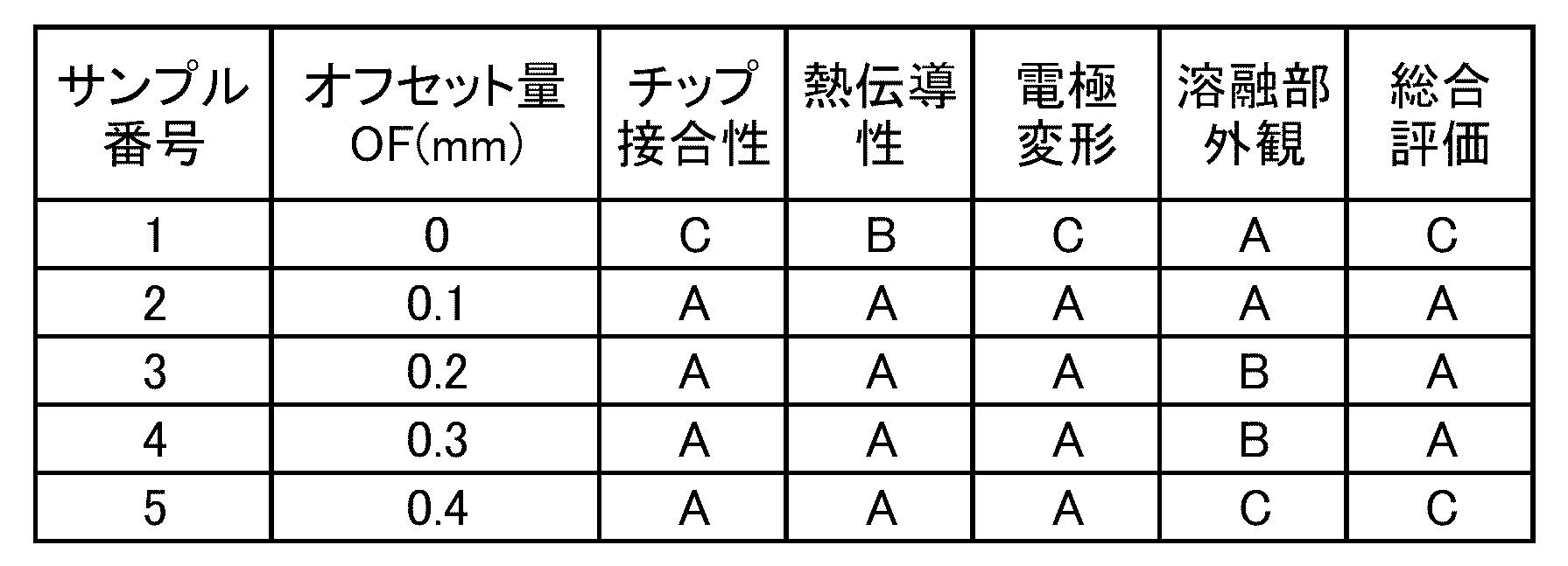
5種類のサンプル1~5では、電極チップ38の軸線CLに対するチップ保持部39の軸線Coの自由端方向FDへのずれ量をオフセット量OFとする(図3、図4)。5種類のサンプル1~5では、オフセット量OFが、それぞれ異なり、0、0.1mm、0.2mm、0.3mm、0.4mmとされている。なお、サンプル1は、オフセット量OFが0であるので、実施形態の点火プラグ100のサンプルではなく、比較用のサンプルである。なお、各サンプルにおいて、電極チップ38は、イリジウム合金を用いて形成され、電極本体33およびチップ保持部39は、ニッケル合金であるインコネル600を用いて形成された。
なお、比較用のサンプル1では、上述した第1部分PT1、第2部分PT2の両方において、溶融部82は、電極チップ38の鍔部382に到達している。また、実施形態の点火プラグ100のサンプル2~5では、上述した第1部分PT1において、溶融部82は、電極チップ38の鍔部382に到達せず、第2部分PT2において、溶融部82は、電極チップ38の鍔部382に到達している。
まず、サンプル1~5の溶融部82の外観の評価を行った。溶融部82が、電極チップ38の側面への付着(いわゆる溶融だれの昇り)が見られないサンプルの評価を「A」とし、電極チップ38の側面への付着が僅かに見られるサンプルの評価を「B」とし、電極チップ38の側面への付着が明らかに発生しているサンプルの評価を「C」とした。
さらに、サンプル1~5について、冷熱試験を行った。冷熱試験では、各サンプルの接地電極30の電極チップ38の近傍に対して、加熱と冷却とのサイクルを1000回繰り返した。1回のサイクルでは、高周波ヒータを用いて、2分間に亘って摂氏950~100度に2分間に亘って加熱し、その後に1分間に亘って空気中で自然冷却を行った。
その後、チップ接合性の評価を行った。具体的には、電極チップ38の浮き上がりや脱落の発生の有無を確認した。確認は、目視と、軸線方向と垂直な方向から見た電極チップ38の外形をトレースした結果を試験の前後にて比較することによって行われた。電極チップ38の浮き上がりや脱落が見られないサンプルの評価を「A」とし、電極チップ38の浮き上がりや脱落が見られたサンプルの評価を「C」とした。
さらに、熱伝導性の評価を行った。具体的には、冷熱試験において2分間の加熱終了後から1分間の冷却による電極チップ38の温度の低下量ΔTを、熱電対を用いて測定した。そして、低下量ΔTの平均値が、100度以上であるサンプルの評価を「A」とし、低下量ΔTの平均値が、50度以上100度未満であるサンプルの評価を「B」とし、低下量ΔTの平均値が、50度未満であるサンプルの評価を「C」とした。
さらに、接地電極30の変形の評価を行った。具体的には、電極本体33の自由端333が、試験の後に、図2の矢印ARで示す方向(すなわち、電極チップ38の軸線CLに沿った先端方向LD)に変形した変形量ΔHを測定した。変形量ΔHが0であるサンプルの評価を「A」とし、変形量ΔHが1mm未満であるサンプルの評価を「B」とし、変形量ΔHが1mm以上であるサンプルの評価を「C」とした。
さらに、総合評価を行った。上記の4個の評価項目に、1個でも「C」評価があるサンプルの評価を「C」とし、上記の4個の評価項目のうち、「C」評価がなく、「A」評価が2個以上あるサンプルの評価「A」とし、それ以外のサンプルの評価を「B」とした。総合評価では、オフセット量OFが0、および、0.4mmであるサンプル1、5の評価は、「C」であり、オフセット量OFが0.1mm以上0.3mm以下であるサンプル2、3、4の評価は、「A」であった。
溶融部82の外観評価では、オフセット量OFが0および0.1mmであるサンプル1、2の評価は、「A」であり、オフセット量OFが0.2mm、0.3mmであるサンプル3、4の評価は、「B」であり、オフセット量OFが0.4mmであるサンプル5の評価は、「C」であった。オフセット量OFが大きくなるほど、接続端方向CD側で、チップ保持部39の外側面391と、電極チップ38の外側面381sと、の距離が近くなるために、溶融部82と電極チップ38とが近づく。このために、溶融部82が電極チップ38に付着しやすくなっているためであると考えられる。
チップ接合性の評価では、オフセット量OFが0であるサンプル1の評価は、「C」であり、オフセット量OFが0.1mm以上0.4mm以下であるサンプル2~5の評価は、「A」であった。この理由は、以下の通りである。接地電極30のうち、接続端方向CD側は、熱引きによって温度が低下するが、自由端方向FD側は、熱引きがないので、温度が低下し難い。このために、接地電極30のうち、自由端方向FD側の温度は、接続端方向CD側の温度より高い。このために、電極チップ38と、チップ保持部39とは、材質が異なるので、熱膨張係数が互いに異なる。具体的には、ニッケル合金製のチップ保持部39の熱膨張係数は、貴金属製の電極チップ38の熱膨張係数より大きい。このために、高温となる自由端方向FD側の第1部分PT1で、溶融部82が電極チップ38に到達していると、この部分において、比較的大きな熱応力が発生する。この結果、熱応力に起因して溶融部82にクラックが発生しやすい。この結果、自由端方向FD側の第1部分PT1で、電極チップ38の浮き上がりや脱落が発生しやすい。このように、オフセット量OFが0であるサンプル1では、より高温の自由端方向FD側の第1部分PT1において、溶融部82が電極チップ38に到達しているために、電極チップ38の浮き上がりや脱落が発生しやすい。一方、オフセット量OFが0でないサンプル2~5では、高温の自由端方向FD側の第1部分PT1において、溶融部82が電極チップ38に到達していないために、電極チップ38の浮き上がりや脱落が発生し難い。
接地電極30の変形の評価では、チップ接合性の評価と同様に、オフセット量OFが0であるサンプル1の評価は、「C」であり、オフセット量OFが0.1mm以上0.4mm以下であるサンプル2~5の評価は、「A」であった。この理由は、以下の通りである。上述したように、より高温となる自由端方向FD側の第1部分PT1で、溶融部82が電極チップ38に到達していると、比較的大きな熱応力が発生する。この熱応力に起因して電極本体33が変形すると考えられる。このように、オフセット量OFが0であるサンプル1では、より高温の自由端方向FD側の第1部分PT1において、溶融部82が電極チップ38に到達しているために、電極本体33の変形が発生しやすい。一方、オフセット量OFが0でないサンプル2~5では、高温の自由端方向FD側の第1部分PT1において、溶融部82が電極チップ38に到達していないために、電極本体33の変形が発生し難い。
熱伝導性の評価では、オフセット量OFが0であるサンプル1の評価は、「B」であり、オフセット量OFが0.1mm以上0.4mm以下であるサンプル2~5の評価は、「A」であった。この理由は、以下のように考えられる。接続端方向CD側の第2部分PT2で、溶融部82が電極チップ38に到達していると、第2部分PT2で、電極チップ38と電極本体33とが、溶融部82を介して接合される。このために、電極チップ38と電極本体33とが単に接触しているだけである場合と比較して、電極チップ38から電極本体33への熱引きが効率的に行われる。オフセット量OFが0であるサンプル1では、接続端方向CD側の第2部分PT2の近傍において、溶融部82が電極チップ38に到達している面積が、オフセット量OFが0でないサンプル2~5と比較して小さい。このために、オフセット量OFが0であるサンプル1は、オフセット量OFが0でないサンプル2~5と比較して、熱引き性能(すなわち、熱伝導性)が劣ると考えられる。
以上の結果から、チップ接合性、熱伝導性、接地電極30の変形の観点からは、オフセット量OFを設けて、第1部分PT1において、溶融部82は、電極チップ38に到達せず、第2部分PT2において、溶融部82は、電極チップ38に到達していることが好ましいことが解った。そして、溶融部82の外観の観点からは、オフセット量OFが過度に大きいことは好ましくない。総合的には、オフセット量OFは、0.1mm以上0.3mm以下が好ましいことが解った。
以上の評価試験からも解るように、溶融部82が接地電極30の自由端333側で、電極チップ38に到達していても、接地電極30の自由端333側は、高温になりやすい上に、自由端であるために、熱引きが期待できない。また、溶融部82が接地電極30の自由端333側で、電極チップ38に到達していると、自由端333側は高温になりやすいので、電極チップ38とチップ保持部39との間の熱膨張係数の差に基づく熱応力によって、溶融部82にクラックが発生しやすい。一方、接地電極30の接続端332側では、溶融部82が電極チップ38に到達していると熱引きが向上する。また、接続端332側は、自由端333側と比較して高温になり難いので、接続端332側では、溶融部82が電極チップ38に到達していても、熱応力による溶融部82のクラックは発生しがたい。このことから、上記実施形態の点火プラグ100によれば、自由端333側の第1部分PT1および接続端332側の第2部分PT2において、溶融部82の軸線方向の長さL1は、凹部335の軸線方向の長さL3より長いので、電極チップ38を十分な強度で保持できる。さらに、第1部分PT1において、溶融部82は、電極チップ38に到達せず、第2部分PT2において、溶融部82は、電極チップ38に到達しているので、熱引きを向上しつつ、溶融部82にクラックが発生する不具合を抑制できる。したがって、高温環境下にて、電極チップの浮き上がりや脱落を抑制することができる。
また、上記実施形態の点火プラグ100では、溶融部82は、チップ保持部39の外側面と、凹部335の内側面と、の境界の全周に亘って形成されている。この結果、高温環境下にて、電極チップの浮き上がりや脱落をより効果的に抑制することができる。
さらに、電極チップ38は、チップ本体381と、鍔部382と、を有しており、第2部分PT2において、溶融部82は、電極チップ38の鍔部382に到達している。このように、電極チップ38は、鍔部382を有するので、電極チップ38を確実に電極本体33に、保持することができる。また、第2部分PT2において、溶融部82を確実に電極チップに到達させることができる。この結果、高温環境下にて、電極チップ38の浮き上がりや脱落をより効果的に抑制することができる。
さらに、上記実施形態の点火プラグ100では、チップ保持部39の軸線Coは、電極チップ38の軸線CLに対して、自由端方向FDにずれている。この結果、第1部分PT1において、溶融部82が、電極チップに到達せず、第2部分PT2において、溶融部82が、電極チップに到達している構成を、容易に実現することができる。
B.第2実施形態
図7は、第2実施形態の接地電極30bの先端部331bの近傍を拡大して示す部分断面図である。図8は、第2実施形態のレーザ溶接前の接地電極30bの先端部331bの分解図である。図8に示すように、第2実施形態では、チップ保持部39bの形状が、第1実施形態のチップ保持部39と異なっている。また、第2実施形態では、電極本体33bに形成された凹部335bの形状が、第1実施形態の凹部335と異なっている。第2実施形態の電極チップ38は、第1実施形態の電極チップ38と同じである。
図7は、第2実施形態の接地電極30bの先端部331bの近傍を拡大して示す部分断面図である。図8は、第2実施形態のレーザ溶接前の接地電極30bの先端部331bの分解図である。図8に示すように、第2実施形態では、チップ保持部39bの形状が、第1実施形態のチップ保持部39と異なっている。また、第2実施形態では、電極本体33bに形成された凹部335bの形状が、第1実施形態の凹部335と異なっている。第2実施形態の電極チップ38は、第1実施形態の電極チップ38と同じである。
図8に示すように、第2実施形態のチップ保持部39bは、円柱状の外形を有している。第2実施形態のチップ保持部39bは、第1実施形態のチップ保持部39(図4)の後端側の孔395aを、貫通孔として有している。そして、第2実施形態のチップ保持部39bは、第1実施形態のチップ保持部39(図4)の先端側の孔395bを有していない。このために、第2実施形態のチップ保持部39bの軸線方向の長さL2bは、第1実施形態のチップ保持部39の軸線方向の長さL2より短い。
第2実施形態の凹部335bは、電極チップ38の鍔部382が嵌合する略円柱形状の先端側部分335b1と、先端側部分335b1より後端側に位置し、先端側部分335b1より大きな径を有する後端側部分335b2と、を有している。後端側部分335b2は、チップ保持部39bが嵌合する略円柱形状を有している。先端側部分335b1の軸線CLは、電極チップ38の軸線CL、および、チップ保持部39bの貫通孔395aの軸線CLと同じである。後端側部分335b2の軸線Coは、チップ保持部39bの円柱状の外形の軸線Coと、同じである。したがって、後端側部分335b2の軸線Coは、先端側部分335b1の軸線CLに対して、自由端方向FDにずれている。後端側部分335b2の軸線方向の長さL3b2は、チップ保持部39bの軸線方向の長さL2bと等しい。また、先端側部分335b1の軸線方向の長さL3b1は、電極チップ38の鍔部382の軸線方向の長さL5と等しい。
図7に示すように、チップ保持部39bが、電極本体33bに対して、レーザ溶接されている結果、貫通孔395aを形成するチップ保持部39bの内面と、凹部335bの底面335b4(すなわち、先端側部分335b1の底面)によって電極チップ38が電極本体33bにおいて保持されている。また、チップ保持部39bは、先端側部分335b1と、後端側部分335b2と、の間に形成された段部335b3によって、支持されている。
そして、第1実施形態と同様に、溶融部82のうち、自由端方向FD側の第1部分PT1の中心CP1から電極チップ38の中心(すなわち、軸線CL)までの距離Dfは、接続端方向CD側の第2部分PT2の中心CP2から電極チップ38の中心までの距離Dcより長い。
そして、第1実施形態と同様に、溶融部82の軸線方向の長さL1(図7)は、全周において、凹部335の軸線方向の長さL3(L3b1+L3b2)より長い。
そして、第1実施形態と同様に、図7において、円C1で示すように、第1部分PT1において、溶融部82は、電極チップ38に到達していない。また、図7において、円C2で示すように、第2部分PT2において、溶融部82は、電極チップ38(具体的には、電極チップ38の鍔部382)に到達している。
第2実施形態においても、第1実施形態と同様に、第1部分PT1において、溶融部82は、電極チップ38に到達せず、第2部分PT2において、溶融部82は、電極チップ38に到達しているので、熱引きを向上しつつ、溶融部82にクラックが発生する不具合を抑制できる。したがって、高温環境下にて、電極チップの浮き上がりや脱落を抑制することができる。
I.変形例:
(1)上記第1実施形態では、溶融部82は、チップ保持部39の外側面と、凹部335の内側面と、の境界の全周に亘って形成されている。これに限らず、溶融部は、凹部335の内側面と、の境界の一部に形成されていても良い。図9は、変形例の接地電極30cの説明図である。図9では、図3と同様に、後端側から先端方向LDを向いて見た接地電極30cの先端部331cの近傍の概略が示されている。
(1)上記第1実施形態では、溶融部82は、チップ保持部39の外側面と、凹部335の内側面と、の境界の全周に亘って形成されている。これに限らず、溶融部は、凹部335の内側面と、の境界の一部に形成されていても良い。図9は、変形例の接地電極30cの説明図である。図9では、図3と同様に、後端側から先端方向LDを向いて見た接地電極30cの先端部331cの近傍の概略が示されている。
図9の接地電極30cでは、溶融部は、自由端方向FD側に位置する第1溶融部82c1と、接続端方向CD側に位置する第2溶融部82c2と、を備えている。そして、図9の接地電極30cの溶融部以外の構成は、第1実施形態と同じである。第1溶融部82c1は、上述した第1の線VL1と交差する第1部分PT1を含み、第2溶融部82c2は、上述した第2の線VL2と交差する第2部分PT2を含んでいる。図9の接地電極30cでは、電極チップ38の軸線CLから見て、上述した第1の線VL1や第2の線VL2と直交する方向には、溶融部は形成されていない。
なお、図9において、第2溶融部82c2のうちの第2部分PT2を中心とした周方向の角度θの範囲内において、第2溶融部82c2は、電極チップ38に到達している。周方向の角度θの範囲外において、第2溶融部82c2は、電極チップ38に到達していない。この電極チップ38に到達している溶融部の範囲を示す角度θは、例えば、160度未満であることが好ましく、30度以上120度未満であることが、さらに、好ましい。
(2)電極チップ38の形状とチップ保持部39、39bの形状としては、上記各実施形態で説明した形状に限らず、他の種々の形状を採用可能である。例えば、電極チップは、鍔部382を備えず、チップ本体381のみを備える構成であっても良い。また、電極チップは、先端方向LDから後端方向BDに向かって、ステップ状に外形が、小さくなっていても良い。
また、チップ保持部39は、後端側から先端方向LDを向いて見た形状が、円でなくても良く、他の形状であっても良い。例えば、チップ保持部39は、後端側から先端方向LDを向いて見た形状が、自由端方向FDの長さが、自由端方向FDと直交する方向の長さより長い楕円であっても良い。また、チップ保持部39は、インコネル600を用いて形成されているが、他の耐熱性を有する材料、例えば、インコネル600とは異なる耐熱ニッケル合金を用いて形成されてもよい。
(3)上記各実施形態では、溶融部は、電極本体33の表面33sに対して直交する方向に延びている。すなわち、上記各実施形態のレーザ溶接では、電極本体33の表面33sに対して直交する方向にレーザが照射されている。これに代えて、溶融部は、電極本体33の表面33sに対して斜めに延びていても良い。たとえば、溶融部は、電極本体33の表面33sから離れた位置ほど(すなわち、深い位置ほど)、電極チップ38の軸線CLに近づくように、斜めに傾斜していても良い。逆に、溶融部は、電極本体33の表面33sから離れた位置ほど(すなわち、深い位置ほど)、電極チップ38の軸線CLから離れるように、斜めに傾斜していても良い。
(4)上記実施例の電極チップ38は、イリジウム合金で形成されているが、イリジウムとは異なる貴金属、あるいは、該貴金属を主成分とする合金で形成されても良い。イリジウムとは異なる貴金属としては、たとえば、白金(Pt)、ロジウム(Rh)が採用され得る。
(5)点火プラグの構成としては、図1で説明した構成に限らず、種々の構成を採用可能である。例えば、中心電極20のうちの間隙gを形成する部分に、電極チップを設けても良い。電極チップの材料としては、イリジウムや白金等の貴金属を含む合金を採用可能である。また、中心電極20の芯材22が省略されてもよい。
以上、実施形態、変形例に基づき本発明について説明してきたが、上記した発明の実施の形態は、本発明の理解を容易にするためのものであり、本発明を限定するものではない。本発明は、その趣旨並びに特許請求の範囲を逸脱することなく、変更、改良され得ると共に、本発明にはその等価物が含まれる。
5...ガスケット、6...第2パッキン、7...第3パッキン、8...第1パッキン、9...タルク、10...絶縁体、11...第2縮外径部、12...軸孔、13...脚部、15...第1縮外径部、16...縮内径部、17...第1胴部、18...第2胴部、19...鍔部、20...電極、20...中心電極、20s1...先端面、21...電極母材、22...芯材、23...頭部、24...鍔部、25...脚部、30、30b、30c...接地電極、33、33b...電極本体、35...母材、36...芯部、38...電極チップ、38s1...放電面、38s2...反対面、39、39b...チップ保持部、40...端子金具、41...キャップ装着部、42...鍔部、43...脚部、50...主体金具、51...工具係合部、52...ネジ部、53...加締部、54...座部、55...胴部、56...縮内径部、58...変形部、59...貫通孔、60...第1シール部、70...抵抗体、80...第2シール部、82...溶融部、100...点火プラグ、331、331b、331c...先端部、332...接続端、333...自由端、335、335b...凹部、381...チップ本体、382...鍔部
Claims (3)
- 中心電極と、
前記中心電極との間に間隙を形成する放電面と、前記放電面より大きな径を有し、前記放電面とは反対側の反対面と、を有する電極チップと、
前記電極チップのうちの一部が内部に配置される貫通孔を有するチップ保持部と、
前記チップ保持部と前記電極チップのうちの前記反対面を含む少なくとも一部分とが配置される凹部を有し、一端が主体金具に接続される接続端であり、他端が自由端である接地電極本体と、
前記チップ保持部の外側面と、前記凹部の内側面と、の境界の少なくとも一部に形成された溶融部と、
を備え、
前記反対面から前記放電面に向かう方向を第1方向とするとき、前記貫通孔の前記第1方向の端の径は、前記放電面の径以上、かつ、前記反対面の径より小さく、
前記貫通孔を形成する前記チップ保持部の内面と、前記凹部の底面と、によって前記電極チップが保持される点火プラグであって、
前記接地電極本体の前記第1方向側の面において、前記電極チップの軸線から前記自由端に向かう方向に延びる仮想線を第1の線とし、前記電極チップの軸線から前記接続端に向かう方向に延びる仮想線を第2の線とするとき、
前記接地電極本体の前記第1方向側の面において、前記溶融部のうち、前記第1の線と交差する第1部分の中心から前記電極チップの中心までの距離は、前記溶融部のうち、前記第2の線と交差する第2部分の中心から前記電極チップの中心までの距離より長く、
前記第1の線と前記電極チップの軸線とを通る断面において、
前記第1部分における前記溶融部の前記第1方向の長さは、前記第1部分における前記凹部の前記第1方向の長さより長く、
前記第2部分における前記溶融部の前記第1方向の長さは、前記第2部分における前記凹部の前記第1方向の長さより長く、
前記第1部分において、前記溶融部は、前記電極チップに到達せず、
前記第2部分において、前記溶融部は、前記電極チップに到達していることを特徴とする、点火プラグ。 - 請求項1に記載の点火プラグであって、
前記溶融部は、前記チップ保持部の外側面と、前記凹部の内側面と、の境界の全周に亘って形成されていることを特徴とする点火プラグ。 - 請求項1または2に記載の点火プラグであって、
電極チップは、前記放電面を含むチップ本体と、前記チップ本体の径より大きな径を有し、前記チップ本体より前記第1方向の反対側に位置し、前記反対面を含む鍔部と、を有し、
前記第2部分において、前記溶融部は、前記電極チップの前記鍔部に到達していることを特徴とする、点火プラグ。
Priority Applications (3)
| Application Number | Priority Date | Filing Date | Title |
|---|---|---|---|
| US15/780,484 US20180351331A1 (en) | 2015-12-03 | 2016-09-13 | Spark plug |
| CN201680070738.2A CN108292827A (zh) | 2015-12-03 | 2016-09-13 | 火花塞 |
| DE112016005549.8T DE112016005549T5 (de) | 2015-12-03 | 2016-09-13 | Zündkerze |
Applications Claiming Priority (2)
| Application Number | Priority Date | Filing Date | Title |
|---|---|---|---|
| JP2015-236307 | 2015-12-03 | ||
| JP2015236307A JP6293107B2 (ja) | 2015-12-03 | 2015-12-03 | 点火プラグ |
Publications (1)
| Publication Number | Publication Date |
|---|---|
| WO2017094210A1 true WO2017094210A1 (ja) | 2017-06-08 |
Family
ID=58796618
Family Applications (1)
| Application Number | Title | Priority Date | Filing Date |
|---|---|---|---|
| PCT/JP2016/004152 Ceased WO2017094210A1 (ja) | 2015-12-03 | 2016-09-13 | 点火プラグ |
Country Status (5)
| Country | Link |
|---|---|
| US (1) | US20180351331A1 (ja) |
| JP (1) | JP6293107B2 (ja) |
| CN (1) | CN108292827A (ja) |
| DE (1) | DE112016005549T5 (ja) |
| WO (1) | WO2017094210A1 (ja) |
Families Citing this family (1)
| Publication number | Priority date | Publication date | Assignee | Title |
|---|---|---|---|---|
| JP6731450B2 (ja) * | 2018-07-11 | 2020-07-29 | 日本特殊陶業株式会社 | スパークプラグ |
Citations (2)
| Publication number | Priority date | Publication date | Assignee | Title |
|---|---|---|---|---|
| JP2009283262A (ja) * | 2008-05-21 | 2009-12-03 | Ngk Spark Plug Co Ltd | スパークプラグ |
| JP2015118910A (ja) * | 2013-11-12 | 2015-06-25 | 日本特殊陶業株式会社 | スパークプラグ、および、スパークプラグの製造方法 |
Family Cites Families (2)
| Publication number | Priority date | Publication date | Assignee | Title |
|---|---|---|---|---|
| JP4402731B2 (ja) * | 2007-08-01 | 2010-01-20 | 日本特殊陶業株式会社 | 内燃機関用スパークプラグ及びスパークプラグの製造方法 |
| US8506341B2 (en) * | 2009-03-31 | 2013-08-13 | Ngk Spark Plug Co., Ltd. | Method of manufacturing sparkplugs |
-
2015
- 2015-12-03 JP JP2015236307A patent/JP6293107B2/ja not_active Expired - Fee Related
-
2016
- 2016-09-13 WO PCT/JP2016/004152 patent/WO2017094210A1/ja not_active Ceased
- 2016-09-13 DE DE112016005549.8T patent/DE112016005549T5/de not_active Withdrawn
- 2016-09-13 US US15/780,484 patent/US20180351331A1/en not_active Abandoned
- 2016-09-13 CN CN201680070738.2A patent/CN108292827A/zh active Pending
Patent Citations (2)
| Publication number | Priority date | Publication date | Assignee | Title |
|---|---|---|---|---|
| JP2009283262A (ja) * | 2008-05-21 | 2009-12-03 | Ngk Spark Plug Co Ltd | スパークプラグ |
| JP2015118910A (ja) * | 2013-11-12 | 2015-06-25 | 日本特殊陶業株式会社 | スパークプラグ、および、スパークプラグの製造方法 |
Also Published As
| Publication number | Publication date |
|---|---|
| JP2017103131A (ja) | 2017-06-08 |
| DE112016005549T5 (de) | 2018-08-23 |
| CN108292827A (zh) | 2018-07-17 |
| US20180351331A1 (en) | 2018-12-06 |
| JP6293107B2 (ja) | 2018-03-14 |
Similar Documents
| Publication | Publication Date | Title |
|---|---|---|
| JP5414896B2 (ja) | スパークプラグ | |
| WO2021111719A1 (ja) | スパークプラグ | |
| JP5905056B2 (ja) | スパークプラグ、および、スパークプラグの製造方法 | |
| JP5475906B2 (ja) | スパークプラグの製造方法 | |
| CN102292887B (zh) | 火花塞 | |
| JP6205006B2 (ja) | スパークプラグ | |
| KR101998536B1 (ko) | 스파크 플러그 | |
| JP6270802B2 (ja) | 点火プラグ | |
| JP6293107B2 (ja) | 点火プラグ | |
| JP6347818B2 (ja) | 点火プラグ | |
| JP5895056B2 (ja) | スパークプラグ | |
| WO2013011723A1 (ja) | スパークプラグ | |
| JP2015022791A (ja) | スパークプラグ及びその製造方法 | |
| JP6557610B2 (ja) | スパークプラグ | |
| JP6456278B2 (ja) | スパークプラグ | |
| JP2013118082A (ja) | スパークプラグ、及び、スパークプラグの製造方法 | |
| JP2010165698A (ja) | スパークプラグ | |
| JP6632576B2 (ja) | 点火プラグ | |
| JP2010165698A5 (ja) | ||
| JP2017111981A (ja) | 点火プラグ | |
| JP2017111983A (ja) | 点火プラグ | |
| JP2013062100A (ja) | スパークプラグ及びその製造方法 |
Legal Events
| Date | Code | Title | Description |
|---|---|---|---|
| 121 | Ep: the epo has been informed by wipo that ep was designated in this application |
Ref document number: 16870153 Country of ref document: EP Kind code of ref document: A1 |
|
| WWE | Wipo information: entry into national phase |
Ref document number: 112016005549 Country of ref document: DE |
|
| 122 | Ep: pct application non-entry in european phase |
Ref document number: 16870153 Country of ref document: EP Kind code of ref document: A1 |