WO2017090174A1 - 無停電電源装置 - Google Patents
無停電電源装置 Download PDFInfo
- Publication number
- WO2017090174A1 WO2017090174A1 PCT/JP2015/083357 JP2015083357W WO2017090174A1 WO 2017090174 A1 WO2017090174 A1 WO 2017090174A1 JP 2015083357 W JP2015083357 W JP 2015083357W WO 2017090174 A1 WO2017090174 A1 WO 2017090174A1
- Authority
- WO
- WIPO (PCT)
- Prior art keywords
- voltage
- phase
- power supply
- detector
- commercial
- Prior art date
- Legal status (The legal status is an assumption and is not a legal conclusion. Google has not performed a legal analysis and makes no representation as to the accuracy of the status listed.)
- Ceased
Links
Images








Classifications
-
- H—ELECTRICITY
- H02—GENERATION; CONVERSION OR DISTRIBUTION OF ELECTRIC POWER
- H02J—ELECTRIC POWER NETWORKS; CIRCUIT ARRANGEMENTS OR SYSTEMS FOR SUPPLYING OR DISTRIBUTING ELECTRIC POWER; SYSTEMS FOR STORING ELECTRIC ENERGY
- H02J9/00—Circuit arrangements for emergency or stand-by power supply, e.g. for emergency lighting
- H02J9/04—Circuit arrangements for emergency or stand-by power supply, e.g. for emergency lighting in which the distribution system is disconnected from the normal source and connected to a standby source
- H02J9/06—Circuit arrangements for emergency or stand-by power supply, e.g. for emergency lighting in which the distribution system is disconnected from the normal source and connected to a standby source with automatic change-over, e.g. UPS systems
- H02J9/062—Circuit arrangements for emergency or stand-by power supply, e.g. for emergency lighting in which the distribution system is disconnected from the normal source and connected to a standby source with automatic change-over, e.g. UPS systems for AC powered loads
-
- G—PHYSICS
- G06—COMPUTING OR CALCULATING; COUNTING
- G06F—ELECTRIC DIGITAL DATA PROCESSING
- G06F1/00—Details not covered by groups G06F3/00 - G06F13/00 and G06F21/00
- G06F1/26—Power supply means, e.g. regulation thereof
- G06F1/263—Arrangements for using multiple switchable power supplies, e.g. battery and AC
-
- G—PHYSICS
- G06—COMPUTING OR CALCULATING; COUNTING
- G06F—ELECTRIC DIGITAL DATA PROCESSING
- G06F1/00—Details not covered by groups G06F3/00 - G06F13/00 and G06F21/00
- G06F1/26—Power supply means, e.g. regulation thereof
- G06F1/28—Supervision thereof, e.g. detecting power-supply failure by out of limits supervision
-
- G—PHYSICS
- G06—COMPUTING OR CALCULATING; COUNTING
- G06F—ELECTRIC DIGITAL DATA PROCESSING
- G06F1/00—Details not covered by groups G06F3/00 - G06F13/00 and G06F21/00
- G06F1/26—Power supply means, e.g. regulation thereof
- G06F1/30—Means for acting in the event of power-supply failure or interruption, e.g. power-supply fluctuations
-
- H—ELECTRICITY
- H02—GENERATION; CONVERSION OR DISTRIBUTION OF ELECTRIC POWER
- H02J—ELECTRIC POWER NETWORKS; CIRCUIT ARRANGEMENTS OR SYSTEMS FOR SUPPLYING OR DISTRIBUTING ELECTRIC POWER; SYSTEMS FOR STORING ELECTRIC ENERGY
- H02J3/00—Circuit arrangements for AC mains or AC distribution networks
- H02J3/38—Arrangements for feeding a single network from two or more generators or sources in parallel; Arrangements for feeding already energised networks from additional generators or sources in parallel
-
- H—ELECTRICITY
- H02—GENERATION; CONVERSION OR DISTRIBUTION OF ELECTRIC POWER
- H02J—ELECTRIC POWER NETWORKS; CIRCUIT ARRANGEMENTS OR SYSTEMS FOR SUPPLYING OR DISTRIBUTING ELECTRIC POWER; SYSTEMS FOR STORING ELECTRIC ENERGY
- H02J7/00—Circuit arrangements for charging or discharging batteries or for supplying loads from batteries
-
- H—ELECTRICITY
- H02—GENERATION; CONVERSION OR DISTRIBUTION OF ELECTRIC POWER
- H02M—APPARATUS FOR CONVERSION BETWEEN AC AND AC, BETWEEN AC AND DC, OR BETWEEN DC AND DC, AND FOR USE WITH MAINS OR SIMILAR POWER SUPPLY SYSTEMS; CONVERSION OF DC OR AC INPUT POWER INTO SURGE OUTPUT POWER; CONTROL OR REGULATION THEREOF
- H02M5/00—Conversion of AC power input into AC power output, e.g. for change of voltage, for change of frequency, for change of number of phases
- H02M5/40—Conversion of AC power input into AC power output, e.g. for change of voltage, for change of frequency, for change of number of phases with intermediate conversion into DC
- H02M5/42—Conversion of AC power input into AC power output, e.g. for change of voltage, for change of frequency, for change of number of phases with intermediate conversion into DC by static converters
- H02M5/44—Conversion of AC power input into AC power output, e.g. for change of voltage, for change of frequency, for change of number of phases with intermediate conversion into DC by static converters using discharge tubes or semiconductor devices to convert the intermediate DC into AC
- H02M5/453—Conversion of AC power input into AC power output, e.g. for change of voltage, for change of frequency, for change of number of phases with intermediate conversion into DC by static converters using discharge tubes or semiconductor devices to convert the intermediate DC into AC using devices of a triode or transistor type requiring continuous application of a control signal
- H02M5/458—Conversion of AC power input into AC power output, e.g. for change of voltage, for change of frequency, for change of number of phases with intermediate conversion into DC by static converters using discharge tubes or semiconductor devices to convert the intermediate DC into AC using devices of a triode or transistor type requiring continuous application of a control signal using semiconductor devices only
-
- H—ELECTRICITY
- H02—GENERATION; CONVERSION OR DISTRIBUTION OF ELECTRIC POWER
- H02M—APPARATUS FOR CONVERSION BETWEEN AC AND AC, BETWEEN AC AND DC, OR BETWEEN DC AND DC, AND FOR USE WITH MAINS OR SIMILAR POWER SUPPLY SYSTEMS; CONVERSION OF DC OR AC INPUT POWER INTO SURGE OUTPUT POWER; CONTROL OR REGULATION THEREOF
- H02M5/00—Conversion of AC power input into AC power output, e.g. for change of voltage, for change of frequency, for change of number of phases
- H02M5/40—Conversion of AC power input into AC power output, e.g. for change of voltage, for change of frequency, for change of number of phases with intermediate conversion into DC
- H02M5/42—Conversion of AC power input into AC power output, e.g. for change of voltage, for change of frequency, for change of number of phases with intermediate conversion into DC by static converters
- H02M5/44—Conversion of AC power input into AC power output, e.g. for change of voltage, for change of frequency, for change of number of phases with intermediate conversion into DC by static converters using discharge tubes or semiconductor devices to convert the intermediate DC into AC
- H02M5/453—Conversion of AC power input into AC power output, e.g. for change of voltage, for change of frequency, for change of number of phases with intermediate conversion into DC by static converters using discharge tubes or semiconductor devices to convert the intermediate DC into AC using devices of a triode or transistor type requiring continuous application of a control signal
- H02M5/458—Conversion of AC power input into AC power output, e.g. for change of voltage, for change of frequency, for change of number of phases with intermediate conversion into DC by static converters using discharge tubes or semiconductor devices to convert the intermediate DC into AC using devices of a triode or transistor type requiring continuous application of a control signal using semiconductor devices only
- H02M5/4585—Conversion of AC power input into AC power output, e.g. for change of voltage, for change of frequency, for change of number of phases with intermediate conversion into DC by static converters using discharge tubes or semiconductor devices to convert the intermediate DC into AC using devices of a triode or transistor type requiring continuous application of a control signal using semiconductor devices only having a rectifier with controlled elements
-
- H—ELECTRICITY
- H02—GENERATION; CONVERSION OR DISTRIBUTION OF ELECTRIC POWER
- H02M—APPARATUS FOR CONVERSION BETWEEN AC AND AC, BETWEEN AC AND DC, OR BETWEEN DC AND DC, AND FOR USE WITH MAINS OR SIMILAR POWER SUPPLY SYSTEMS; CONVERSION OF DC OR AC INPUT POWER INTO SURGE OUTPUT POWER; CONTROL OR REGULATION THEREOF
- H02M7/00—Conversion of AC power input into DC power output; Conversion of DC power input into AC power output
- H02M7/42—Conversion of DC power input into AC power output without possibility of reversal
- H02M7/44—Conversion of DC power input into AC power output without possibility of reversal by static converters
- H02M7/48—Conversion of DC power input into AC power output without possibility of reversal by static converters using discharge tubes with control electrode or semiconductor devices with control electrode
- H02M7/4807—Conversion of DC power input into AC power output without possibility of reversal by static converters using discharge tubes with control electrode or semiconductor devices with control electrode having a high frequency intermediate AC stage
-
- H—ELECTRICITY
- H02—GENERATION; CONVERSION OR DISTRIBUTION OF ELECTRIC POWER
- H02M—APPARATUS FOR CONVERSION BETWEEN AC AND AC, BETWEEN AC AND DC, OR BETWEEN DC AND DC, AND FOR USE WITH MAINS OR SIMILAR POWER SUPPLY SYSTEMS; CONVERSION OF DC OR AC INPUT POWER INTO SURGE OUTPUT POWER; CONTROL OR REGULATION THEREOF
- H02M7/00—Conversion of AC power input into DC power output; Conversion of DC power input into AC power output
- H02M7/42—Conversion of DC power input into AC power output without possibility of reversal
- H02M7/44—Conversion of DC power input into AC power output without possibility of reversal by static converters
- H02M7/48—Conversion of DC power input into AC power output without possibility of reversal by static converters using discharge tubes with control electrode or semiconductor devices with control electrode
- H02M7/53—Conversion of DC power input into AC power output without possibility of reversal by static converters using discharge tubes with control electrode or semiconductor devices with control electrode using devices of a triode or transistor type requiring continuous application of a control signal
- H02M7/537—Conversion of DC power input into AC power output without possibility of reversal by static converters using discharge tubes with control electrode or semiconductor devices with control electrode using devices of a triode or transistor type requiring continuous application of a control signal using semiconductor devices only, e.g. single switched pulse inverters
- H02M7/5387—Conversion of DC power input into AC power output without possibility of reversal by static converters using discharge tubes with control electrode or semiconductor devices with control electrode using devices of a triode or transistor type requiring continuous application of a control signal using semiconductor devices only, e.g. single switched pulse inverters in a bridge configuration
-
- H—ELECTRICITY
- H02—GENERATION; CONVERSION OR DISTRIBUTION OF ELECTRIC POWER
- H02M—APPARATUS FOR CONVERSION BETWEEN AC AND AC, BETWEEN AC AND DC, OR BETWEEN DC AND DC, AND FOR USE WITH MAINS OR SIMILAR POWER SUPPLY SYSTEMS; CONVERSION OF DC OR AC INPUT POWER INTO SURGE OUTPUT POWER; CONTROL OR REGULATION THEREOF
- H02M3/00—Conversion of DC power input into DC power output
- H02M3/22—Conversion of DC power input into DC power output with intermediate conversion into AC
- H02M3/24—Conversion of DC power input into DC power output with intermediate conversion into AC by static converters
- H02M3/28—Conversion of DC power input into DC power output with intermediate conversion into AC by static converters using discharge tubes with control electrode or semiconductor devices with control electrode to produce the intermediate AC
- H02M3/325—Conversion of DC power input into DC power output with intermediate conversion into AC by static converters using discharge tubes with control electrode or semiconductor devices with control electrode to produce the intermediate AC using devices of a triode or a transistor type requiring continuous application of a control signal
- H02M3/335—Conversion of DC power input into DC power output with intermediate conversion into AC by static converters using discharge tubes with control electrode or semiconductor devices with control electrode to produce the intermediate AC using devices of a triode or a transistor type requiring continuous application of a control signal using semiconductor devices only
- H02M3/33569—Conversion of DC power input into DC power output with intermediate conversion into AC by static converters using discharge tubes with control electrode or semiconductor devices with control electrode to produce the intermediate AC using devices of a triode or a transistor type requiring continuous application of a control signal using semiconductor devices only having several active switching elements
- H02M3/33576—Conversion of DC power input into DC power output with intermediate conversion into AC by static converters using discharge tubes with control electrode or semiconductor devices with control electrode to produce the intermediate AC using devices of a triode or a transistor type requiring continuous application of a control signal using semiconductor devices only having several active switching elements having at least one active switching element at the secondary side of an isolation transformer
- H02M3/33584—Bidirectional converters
-
- H—ELECTRICITY
- H02—GENERATION; CONVERSION OR DISTRIBUTION OF ELECTRIC POWER
- H02M—APPARATUS FOR CONVERSION BETWEEN AC AND AC, BETWEEN AC AND DC, OR BETWEEN DC AND DC, AND FOR USE WITH MAINS OR SIMILAR POWER SUPPLY SYSTEMS; CONVERSION OF DC OR AC INPUT POWER INTO SURGE OUTPUT POWER; CONTROL OR REGULATION THEREOF
- H02M3/00—Conversion of DC power input into DC power output
- H02M3/22—Conversion of DC power input into DC power output with intermediate conversion into AC
- H02M3/44—Conversion of DC power input into DC power output with intermediate conversion into AC by combination of static with dynamic converters; by combination of dynamo-electric with other dynamic or static converters
Definitions
- This invention relates to an uninterruptible power supply, and more particularly to a two-phase three-wire uninterruptible power supply.
- the two-phase three-wire system is a power feeding method that supplies a two-phase AC voltage and a neutral point voltage to a consumer.
- the phases of the two-phase AC voltage are shifted from each other by 180 degrees, which is called a single-phase three-wire system.
- One-phase AC voltage and neutral point voltage of the two-phase AC voltage are supplied to the 100 V electrical device.
- a two-phase AC voltage is supplied to the 200V electric device.
- the two-phase AC voltage of the three-phase AC voltage is supplied to the consumer, and the phases of the two-phase AC voltage are shifted from each other by 120 degrees.
- Patent Document 1 JP-A-6-253549 discloses a single-phase three-wire uninterruptible power supply. This uninterruptible power supply converts a two-phase AC voltage supplied from a commercial AC power source into a DC voltage, and converts a DC voltage generated by the converter or a DC voltage of a power storage device into a two-phase AC voltage. And an inverter for supplying the load.
- a voltage detector that detects an instantaneous value of a two-phase AC voltage from a commercial AC power supply is provided, and a converter and an inverter are controlled in synchronization with an output signal of the voltage detector.
- an abnormality occurs in the voltage detector, the operation of the converter is stopped and the operation of the inverter is continued, and the DC voltage of the power storage device is converted into a two-phase AC voltage and supplied to the load.
- the voltage between the terminals of the power storage device drops and reaches the end-of-discharge voltage, the supply of the two-phase AC voltage from the inverter to the load is stopped, and then the two-phase AC voltage from the commercial AC power supply To be supplied directly to the load.
- the conventional uninterruptible power supply has a problem that the supply of the two-phase AC voltage to the load is momentarily interrupted when the voltage detector fails.
- a main object of the present invention is to provide an uninterruptible power supply that can supply a two-phase AC voltage to a load without interruption even when an abnormality occurs in the voltage detector. .
- An uninterruptible power supply is a two-phase three-wire uninterruptible power supply, which converts a two-phase AC voltage supplied from a commercial AC power source into a DC voltage, and a DC generated by the converter.
- An inverter that converts the DC voltage supplied from the voltage or power storage device into a two-phase AC voltage and supplies it to the load, and one terminal pair receives the two-phase AC voltage from the commercial AC power supply and the other terminal pair is connected to the load
- the control circuit When the first voltage detector is normal, the control circuit turns off the bypass switch pair and the semiconductor switch pair, and controls the converter and the inverter in synchronization with the output signal of the first voltage detector.
- the control circuit stops the operation of the converter, controls the inverter in synchronization with the output signal of the second voltage detector, and controls the DC voltage of the power storage device.
- the phase of the two-phase AC voltage is made to coincide with the phase of the two-phase AC voltage from the commercial AC power source, and the voltage between the terminals of the power storage device decreases to reach a predetermined voltage. Accordingly, the bypass switch pair and the semiconductor switch pair are turned on, and the semiconductor switch pair is turned off after a predetermined time has elapsed.
- Another uninterruptible power supply is a two-phase three-wire uninterruptible power supply, which is a converter that converts a two-phase AC voltage supplied from a commercial AC power source into a DC voltage, and is generated by the converter.
- An inverter that converts the DC voltage or the DC voltage supplied from the power storage device into a two-phase AC voltage and supplies it to the load, and one terminal pair receives the two-phase AC voltage from the commercial AC power supply and the other terminal pair loads.
- the control circuit When the first voltage detector is normal, the control circuit turns off the bypass switch pair and the semiconductor switch pair, and controls the converter and the inverter in synchronization with the output signal of the first voltage detector.
- the control circuit stops the operation of the converter, controls the inverter in synchronization with the output signal of the second voltage detector, and controls the DC voltage of the power storage device.
- the phase of the two-phase AC voltage is made to coincide with the phase of the two-phase AC voltage from the commercial AC power source, and the voltage between the terminals of the power storage device decreases to reach a predetermined voltage. Accordingly, the bypass switch pair and the semiconductor switch pair are turned on, and the semiconductor switch pair is turned off after a predetermined time has elapsed.
- the inverter when the first voltage detector becomes abnormal, the inverter is controlled in synchronization with the output signal of the second voltage detector, and the DC voltage of the power storage device is The phase change of the two-phase AC voltage is made to coincide with the phase of the two-phase AC voltage from the commercial AC power supply, and the bypass switch pair is changed in response to the voltage between the terminals of the power storage device being reduced to a predetermined voltage. And the semiconductor switch pair is turned on. Therefore, even when the first voltage detector becomes abnormal, the two-phase AC voltage can be supplied to the load without interruption.
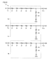
- FIG. 2 is a circuit diagram showing a configuration of an input voltage detection circuit shown in FIG. 1. It is a block diagram which shows the structure of the abnormality detector shown in FIG. It is a circuit diagram for demonstrating abnormality of the voltage detector shown in FIG.
- FIG. 2 is a circuit diagram showing a configuration of an output voltage detection circuit shown in FIG. 1.
- FIG. 2 is a circuit block diagram showing a main part of the control circuit shown in FIG. 1. It is a time chart for demonstrating operation
- FIG. It is a figure which shows operation
- FIG. It is another figure which shows operation
- FIG. It is a circuit block diagram which shows the structure of the input voltage detection circuit contained in the uninterruptible power supply by Embodiment 2 of this invention. It is a circuit block diagram which shows the principal part of the control circuit contained in the uninterruptible power supply demonstrated in FIG.
- FIG. 1 is a circuit block diagram showing a configuration of an uninterruptible power supply according to Embodiment 1 of the present invention.
- this uninterruptible power supply is a two-phase three-wire system, and includes input terminals TI1 to TI3, battery terminals TB1 and TB2, and output terminals TO1 to TO3.
- Input terminals TI1 to TI3 receive AC voltage VI1, AC voltage VI2, and neutral point voltage VN supplied from commercial AC power supply 51, respectively.
- the phase of AC voltage VI1 is 180 degrees ahead of the phase of AC voltage VI2.
- the effective value of each of AC voltages VI1 and VI2 is 100V.
- the neutral point voltage VN is 0V.
- the battery terminals TB1 and TB2 are connected to the positive electrode and the negative electrode of the battery 52 (power storage device), respectively.
- a capacitor may be connected instead of the battery 52.
- An AC voltage VO1, an AC voltage VO2, and a neutral point voltage VN are output to the output terminals TO1 to TO3, respectively, and a load 53 is connected.
- the phase of AC voltage VO1 is 180 degrees ahead of the phase of AC voltage VO2.
- the load 53 receives an AC voltage of 100V from the output terminals TO1 and TN, another electric device receiving an AC voltage of 100V from the output terminals TO2 and TN, and an AC voltage of 200V from the output terminals TO1 and TO2. And other electric devices.
- This uninterruptible power supply further includes switches S1 to S8, semiconductor switches S9 and S10, converter 1, DC positive bus L1, DC negative bus L2, DC neutral point bus L3, smoothing capacitors C1 and C2, and DC voltage detector.
- DT1 to DT3, bidirectional chopper 2, inverter 3, input voltage detection circuit 4, abnormality detector 5, output voltage detection circuit 6, and control circuit 7 are provided.
- the one terminals of the switches S1 and S2 are connected to the input terminals TI1 and TI2, respectively, and the other terminals are connected to the converter 1.
- Input terminal TI3 is connected to DC neutral point bus L3 via converter 1.
- the switches S1 and S2 are controlled by the control circuit 7, and are normally turned on when the two-phase AC power is supplied from the commercial AC power source 51, and the supply of the two-phase AC power from the commercial AC power source 51 is stopped. When the input voltage detection circuit 4 has an abnormality, the input voltage detection circuit 4 is turned off.
- the converter 1 is controlled by the control circuit 7 and converts the two-phase AC power from the commercial AC power source 51 into DC power during normal times when the two-phase AC power is supplied from the commercial AC power source 51.
- converter 1 normally generates positive voltage VD1 and negative voltage VD2 based on two-phase AC voltages VI1 and VI2 supplied from commercial AC power supply 51.
- Converter 1 stops operation of converter 1 at the time of power failure when supply of two-phase AC power from commercial AC power supply 51 is stopped. When an abnormality occurs in the input voltage detection circuit 4, the operation of the converter 1 is stopped.
- DC positive bus L1 is connected between converter 1 and inverter 3 to transmit positive voltage VD1.
- DC negative bus L2 is connected between converter 1 and inverter 3 and transmits negative voltage VD2.
- DC neutral point bus L3 is connected between converter 1 and inverter 3 and transmits neutral point voltage VN.
- the smoothing capacitor C1 is connected between the buses L1 and L3, and smoothes the voltage between the buses L1 and L3.
- Smoothing capacitor C2 is connected between buses L3 and L2, and smoothes the voltage between buses L3 and L2.
- the DC voltage detector DT1 detects the voltage across the terminals of the smoothing capacitor C1 and outputs a signal indicating the detected value to the control circuit 7.
- the detected value of the DC voltage detector DT1 is used to set the voltage across the smoothing capacitor C1 to the target capacitor voltage VCT.
- the DC voltage detector DT2 detects the voltage across the smoothing capacitor C2, and outputs a signal indicating the detected value to the control circuit 7.
- the detection value of the DC voltage detector DT2 is used to set the voltage across the smoothing capacitor C2 to the target capacitor voltage VCT.
- switches S3 and S4 are connected to battery terminals TB1 and TB2, respectively, and the other terminals are connected to buses L1 to L3 via bidirectional chopper 2. Switches S3 and S4 are turned on when the uninterruptible power supply is in use, and are turned off during maintenance of the uninterruptible power supply and battery 52, for example.
- the DC voltage detector DT3 detects the voltage VB between the terminals of the battery 52 and outputs a signal indicating the detected value to the control circuit 7.
- the detection value of the DC voltage detector DT3 detects that the inter-terminal voltage VB of the battery 52 becomes the target battery voltage VBT when the battery 52 is charged and that the inter-terminal voltage VB of the battery 52 has reached the end-of-discharge voltage VBL. Used to do.
- the bidirectional chopper 2 is controlled by the control circuit 7 and stores the DC power generated by the converter 1 in the battery 52 in the normal time when the two-phase AC power is supplied from the commercial AC power supply 51.
- the bidirectional chopper 2 supplies the DC power of the battery 52 to the inverter 3 at the time of a power failure when the supply of the two-phase AC power from the commercial AC power supply 51 is stopped and when an abnormality occurs in the input voltage detection circuit 4.
- the bidirectional chopper 2 normally causes a direct current to flow from each of the capacitors C1 and C2 to the battery 52 to set the inter-terminal voltage VB of the battery 52 to the target battery voltage VBT.
- the bidirectional chopper 2 causes a current to flow from the battery 52 to each of the capacitors C1 and C2 at the time of a power failure and when an abnormality occurs in the input voltage detection circuit 4, and the voltage between the terminals of the capacitors C1 and C2 is set to the target capacitor voltage. VCT.
- the bidirectional chopper 2 When the direct current power of the battery 52 is discharged to the capacitors C1 and C2, the bidirectional chopper 2 reduces the voltage VB between the terminals of the battery 52 and reaches the discharge end voltage VBL. Stop the supply of DC power to the C1 and C2 sides.
- the inverter 3 is controlled by the control circuit 7 and converts the DC power generated by the converter 1 into two-phase AC power during normal times when two-phase AC power is supplied from the commercial AC power supply 51.
- the inverter 3 converts the DC power supplied from the battery 52 via the bidirectional chopper 2 into two-phase AC power during a power failure and when an abnormality occurs in the input voltage detection circuit 4.
- inverter 3 normally supplies two-phase AC voltages VO1, VO2 based on positive voltage VD1, negative voltage VD2, and neutral point voltage VN supplied from converter 1 via buses L1-L3. Generate.
- the inverter 3 is based on the positive voltage VD1, the negative voltage VD2, and the neutral point voltage VN supplied from the bidirectional chopper 2 via the buses L1 to L3 at the time of power failure and when an abnormality occurs in the input voltage detection circuit 4.
- the two-phase AC voltages VO1 and VO2 are generated.
- the one terminals of the switches S5 and S6 are connected to the inverter 3, and the other terminals thereof are connected to the output terminals TO1 and TO2, respectively.
- Output terminal TO3 is connected to DC neutral point bus L3 via inverter 3.
- the switches S5 and S6 are controlled by the control circuit 7 and are turned on in the inverter power supply mode in which the two-phase AC power generated by the inverter 3 is supplied to the load 53, and the two-phase AC power from the commercial AC power source 51 is supplied to the load 53. It is turned off in the bypass power supply mode for direct supply.
- converter 1 includes forward conversion circuits 1a and 1b
- inverter 3 includes reverse conversion circuits 3a and 3b.
- Forward conversion circuit 1a includes transistors Q1, Q2, diodes D1, D2, a reactor 11, and a capacitor 12.
- Forward conversion circuit 1b includes transistors Q3 and Q4, diodes D3 and D4, a reactor 13, and a capacitor 14.
- Inverse conversion circuit 3a includes transistors Q5 and Q6, diodes D5 and D6, a reactor 15, and a capacitor 16.
- Inverse conversion circuit 3b includes transistors Q7 and Q8, diodes D7 and D8, a reactor 17 and a capacitor 18.
- Each of the transistors Q1 to Q8 is, for example, an IGBT (Insulated Gate Bipolar Transistor).
- Transistors Q1, Q3, Q5, Q7 have collectors connected to DC positive bus L1, and transistors Q1, Q3, Q5, Q7 have emitters connected to the collectors of transistors Q2, Q4, Q6, Q8, respectively.
- Q6, Q8 are both connected to the DC negative bus L2.
- Each of the transistors Q1 to Q8 is PWM (Pulse Width Modulation) controlled by the control circuit 7.
- Diodes D1-D8 are connected in antiparallel to transistors Q1-Q8, respectively.
- Reactors 11 and 13 have one terminals connected to the emitters of transistors Q1 and Q3, respectively, and the other terminals connected to the other terminals of switches S1 and S2, respectively, and DC neutral points via capacitors 12 and 14, respectively.
- Reactors 15 and 17 have one terminals connected to the emitters of transistors Q5 and Q7, respectively, the other terminals connected to one terminals of switches S5 and S6, respectively, and DC neutral points via capacitors 16 and 18, respectively. Connected to bus L3.
- the forward conversion circuit 1a when the transistor Q1 is turned on while the AC voltage VI1 supplied from the commercial AC power supply 51 to the input terminal TI1 is a positive voltage, the input terminal TI1, the switch S1, the reactor 11, the transistor Q1, and the DC Current flows through the path of the positive bus L1, the capacitor C1, the DC neutral point bus L3, and the input terminal TI3. As a result, capacitor C1 is charged and positive DC voltage VD1 is supplied to DC positive bus L1.
- Reactor 11 and capacitor 12 constitute a low-pass filter, and a commercial frequency AC voltage VI1 supplied from commercial AC power supply 51 is passed through transistors Q1 and Q2, and a switching frequency signal generated in transistors Q1 and Q2 is generated. The passage to the commercial AC power supply 51 side is prevented.
- the forward conversion circuit 1b when the transistor Q3 is turned on while the AC voltage VI2 supplied from the commercial AC power supply 51 to the input terminal TI2 is a positive voltage, the input terminal TI2, the switch S2, the reactor 13, the transistor Q3, the DC Current flows through the path of the positive bus L1, the capacitor C1, the DC neutral point bus L3, and the input terminal TI3. As a result, capacitor C1 is charged and positive DC voltage VD1 is supplied to DC positive bus L1.
- Reactor 13 and capacitor 14 constitute a low-pass filter, and a commercial frequency AC voltage VI2 supplied from commercial AC power supply 51 is passed through transistors Q3 and Q4, and a switching frequency signal generated in transistors Q3 and Q4 is generated. The passage to the commercial AC power supply 51 side is prevented.
- the forward conversion circuit 1a converts the AC voltage VI1 into DC voltages VD1 and VD2, and converts AC power into DC power.
- the forward conversion circuit 1b converts the AC voltage VI2 into DC voltages VD1 and VD2, and converts AC power into DC power.
- Reactor 15 and capacitor 16 constitute a low-pass filter, and allow commercial frequency AC voltage VO1 generated by transistors Q5 and Q6 to pass through load 53.
- a signal of switching frequency generated by transistors Q5 and Q6 is received by load 53. Prevent passing to the side.
- reactor 15 and capacitor 16 convert rectangular wave-shaped AC voltage generated by turning on / off each of transistors Q5 and Q6 into sine-wave-shaped AC voltage VO1 and apply it to load 53.
- Reactor 17 and capacitor 18 constitute a low-pass filter, and the commercial frequency AC voltage VO2 generated by transistors Q7 and Q8 is passed through load 53, and the switching frequency signal generated by transistors Q7 and Q8 is the load 53. Prevent passing to the side.
- the reactor 17 and the capacitor 18 convert a rectangular wave-shaped AC voltage generated by turning on / off the transistors Q7 and Q8 into a sinusoidal AC voltage VO2 and apply it to the load 53.
- the inverse conversion circuit 3a converts the DC voltages VD1 and VD2 into an AC voltage VO1, and converts DC power into AC power.
- Inverse conversion circuit 3b converts DC voltages VD1 and VD2 into AC voltage VO2, and converts DC power into AC power.
- one terminals of the switches S7 and S8 are connected to the input terminals TI1 and TI2, respectively, and the other terminals thereof are connected to the output terminals TO1 and TO2, respectively.
- Semiconductor switches S9 and S10 are connected in parallel to switches S7 and S8, respectively.
- Each of semiconductor switches S9 and S10 includes, for example, thyristors connected in antiparallel to each other.
- the input terminal TI3 is directly connected to the output terminal TO3.
- the switches S7 and S8 are controlled by the control circuit 7 and are turned off in the inverter power supply mode in which the two-phase AC power generated by the inverter 3 is supplied to the load 53, and the two-phase AC power from the commercial AC power source 51 is supplied to the load 53. It is turned on in the bypass power supply mode that supplies directly.
- the semiconductor switches S9 and S10 are turned on for a predetermined time when switching from the inverter power supply mode to the bypass power supply mode.
- the response speed of the semiconductor switches S9 and S10 is sufficiently faster than the response speed of the switches S7 and S8.
- the reason why the semiconductor switches S9 and S10 are turned on for a predetermined time is to prevent the semiconductor switches S9 and S10 from being damaged by the heat generated in the semiconductor switches S9 and S10.
- the semiconductor switches S9 and S10 are instantaneously turned on, and the two-phase AC power from the commercial AC power supply 51 is supplied to the load 53 via the semiconductor switches S9 and S10. .
- the switches S7 and S8 having a slow response time are turned on, the switches S5 and S6 having a slow response time are turned off, and then the semiconductor switches S9 and S10 are turned off.
- the input voltage detection circuit 4 detects the voltages VI1, VI2, and VN of the input terminals TI1 to TI3, and gives a signal indicating the detection value to the control circuit 7.
- the abnormality detector 5 determines whether or not the portion of the input voltage detection circuit 4 corresponding to the input voltage VI1 is normal, and outputs a signal ⁇ 5 indicating the determination result to the control circuit 7.
- the output voltage detection circuit 6 detects the voltages VO1, VO2, and VN of the output terminals TO1 to TO3, and gives a signal indicating the detection value to the control circuit 7.
- the control circuit 7 controls the entire uninterruptible power supply based on the output signals of the input voltage detection circuit 4, the abnormality detector 5, the output voltage detection circuit 6, and the DC voltage detectors DT1 to DT3.
- the input voltage detection circuit 4 includes input terminals T1 to T3, output terminals T11 to T13, and voltage detectors 4a to 4c.
- Input terminals T1 to T3 are connected to input terminals TI1 to TI3, respectively, and receive AC voltage VI1, AC voltage VI2, and neutral point voltage VN, respectively.
- the voltage detector 4a is connected in series between a plurality (five in the figure) of resistive elements 21 connected in series between the input terminal T1 and the output terminal T11, and between the output terminal T11 and the line of the reference voltage VSS.
- An AC voltage VI1D obtained by dividing the AC voltage VI1 at a predetermined voltage dividing ratio appears at the output terminal T11.
- Each of the voltage detectors 4b and 4c has the same configuration as the voltage detector 4a.
- An AC voltage VI2D obtained by dividing the AC voltage VI2 at a predetermined voltage dividing ratio appears at the output terminal T12.
- a voltage VND obtained by dividing the neutral point voltage VN by a predetermined voltage division ratio appears at the output terminal T13.
- the voltages VI1D, VI2D, and VND of the output terminals T11 to T13 are given to the control circuit 7 as output signals of the voltage detectors 4a to 4c, respectively.
- the output signal VI1D of the voltage detector 4a is used for controlling each of the transistors Q1 to Q8 included in the converter 1 and the inverter 3, that is, for controlling the phases of the output voltages VO1 and VO2.
- the output signal VI2D of the voltage detector 4b indicates that the effective value of the AC voltage VI2 is out of the allowable range, that is, the supply of the two-phase AC power from the commercial AC power supply 51 is stopped (a power failure has occurred). Used to detect.
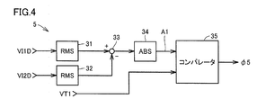
- the abnormality detector 5 includes effective value calculators (RMS) 31 and 32, a subtractor 33, an absolute value calculator (ABS) 34, and a comparator 35.
- the effective value calculation unit 31 calculates the effective value of the output signal VI1D of the voltage detector 4a.
- the effective value calculation unit 32 calculates the effective value of the output signal VI2D of the voltage detector 4b.
- the subtractor 33 calculates the difference between the effective value of the signal VI1D calculated by the effective value calculation unit 31 and the effective value of the signal VI2D calculated by the effective value calculation unit 32.
- the absolute value calculator 34 calculates the absolute value A1 of the difference between the effective value of the signal VI1D obtained by the subtractor 33 and the effective value of the signal VI2D.
- the comparator 35 compares the absolute value A1 calculated by the absolute value calculator 34 with the threshold value VT1, and when A1 ⁇ VT1, sets the abnormality detection signal ⁇ 5 to the “L” level of the inactivation level, and A1> In the case of VT1, the abnormality detection signal ⁇ 5 is set to the activation level “H” level.
- the absolute value A1 is 0, and A1 ⁇ VT1, and the abnormality detection signal ⁇ 5 is inactivated at “ L "level.
- the absolute value A1 becomes a large value, and A1> VT1, so that the abnormality detection signal ⁇ 5 has an activation level “ H ”level.
- the probability that abnormality will occur simultaneously in the voltage detectors 4a and 4b is extremely low.
- the effective value of the output signal VI2D of the voltage detector 4b exceeds the allowable range, so it is determined that a power failure has occurred. Therefore, when abnormality detection signal ⁇ 5 is set to “H” level, abnormality has occurred in voltage detector 4a.
- FIGS. 5A to 5D are diagrams showing a case where an abnormality has occurred in the voltage detector 4a.
- FIG. 5A shows a case where the resistance element 21 is torn. In this case, the signal VI1D becomes 0V, the effective value of the signal VI1D decreases compared to the case where the voltage detector 4a is normal, and the abnormality detection signal ⁇ 5 becomes the “H” level of the activation level.
- FIG. 5B shows a case where the resistance element 22 is torn. In this case, the AC voltage VI1 becomes the signal VI1D as it is, the effective value of the signal VI1D increases as compared with the case where the voltage detector 4a is normal, and the abnormality detection signal ⁇ 5 becomes the activation level “H” level.
- FIG. 5C shows a case where the terminals of the resistance element 21 are short-circuited.
- the effective value of the signal VI1D increases as compared with the case where the voltage detector 4a is normal, and the abnormality detection signal ⁇ 5 becomes the activation level “H” level.
- FIG. 5D shows a case where the terminals of the resistance element 22 are short-circuited. In this case, the effective value of the signal VI1D is reduced as compared with the case where the voltage detector 4a is normal, and the abnormality detection signal ⁇ 5 becomes the activation level “H” level.
- the output voltage detection circuit 6 includes input terminals T21 to T23, output terminals T31 to T33, and voltage detectors 6a to 6c.
- Input terminals T21 to T23 are connected to output terminals TO1 to TO3, respectively, and receive AC voltage VO1, AC voltage VO2, and neutral point voltage VN, respectively.
- the voltage detector 6a is connected in series between a plurality (five in the figure) of resistive elements 21 connected in series between the input terminal T21 and the output terminal T31, and between the output terminal T31 and the line of the reference voltage VSS.
- a plurality of (two in the figure) resistance elements 22 are connected in series between a plurality (five in the figure) of resistive elements 21 connected in series between the input terminal T21 and the output terminal T31, and between the output terminal T31 and the line of the reference voltage VSS.
- a plurality of (two in the figure) resistance elements 22 An AC voltage VO1D obtained by dividing the AC voltage VO1 at a predetermined voltage dividing ratio appears at the output terminal T21.
- Each of the voltage detectors 6b and 6c has the same configuration as the voltage detector 6a.
- An AC voltage VO2D obtained by dividing the AC voltage VO2 at a predetermined voltage dividing ratio appears at the output terminal T32.
- a voltage VND obtained by dividing the neutral point voltage VN by a predetermined voltage dividing ratio appears at the output terminal T33.
- the voltages VO1D, VO2D, and VND of the output terminals T31 to T33 are given to the control circuit 7 as output signals of the voltage detectors 6a to 6c, respectively.
- the control circuit 7 outputs the output signals VI1D, VI2D, and VND of the voltage detectors 4a to 4c, the output signal ⁇ 5 of the abnormality detector 5, the output signals VO1D, VO2D, and VND of the voltage detectors 6a to 6c, and the DC voltage detectors DT1 to DT1. Based on the output signal of DT3, the whole uninterruptible power supply is controlled.
- control circuit 7 controls converter 1 in synchronization with output signal VI1D of voltage detector 4a, and AC voltage VI1 is converted into DC voltages VD1 and VD2, and AC voltage VI2 is converted into DC voltages VD1 and VD2.
- the control circuit 7 controls the inverter 3 so that the phase of the output signal VO1D of the voltage detector 6a matches the phase of the output signal VI1D of the voltage detector 4a.
- the control circuit 7 stops the operation of the converter 1, fixes the transistors Q1 to Q4 in the OFF state, and switches S1, S2 is turned off.
- the control circuit 7 controls the bidirectional chopper 2 to charge each of the capacitors C1 and C2 with the DC power of the battery 52.
- the control circuit 7 controls the inverter 3 so that the phase of the output signal VO1D of the voltage detector 6a matches the phase of the monitor signal obtained by advancing the phase of the output signal VI2D of the voltage detector 4b by 180 degrees.
- the control circuit 7 stops the operation of the bidirectional chopper 2 and turns on the semiconductor switches S9 and S10 and the switches S7 and S8.
- the switches S5 and S6 are turned off. As a result, the two-phase AC power from the commercial AC power supply 51 is supplied to the load 53 without interruption.
- the control circuit 7 turns on the semiconductor switches S9 and S10 and the switches S7 and S8 and turns off the switches S5 and S6. As a result, the two-phase AC power from the commercial AC power supply 51 is supplied to the load 53 without interruption.
- the control circuit 7 stops the operation of the converter 1 and turns off the transistors Q1 to Q4. And switches S1 and S2 are turned off.
- the control circuit 7 controls the bidirectional chopper 2 to charge each of the capacitors C1 and C2 with the DC power of the battery 52.
- the control circuit 7 stores the phase of the output signal VI1D of the voltage detector 4a before the occurrence of the power failure, and the inverter 3 so that the phase of the output signal VO1D of the voltage detector 6a matches the phase of the stored signal VI1D. To control. When the inter-terminal voltage VB of the battery 52 decreases and reaches the discharge end voltage VBL, the control circuit 7 stops the operation of the bidirectional chopper 2 and the inverter 3 and turns off the switches S5 and S6. Therefore, even when a power failure occurs, the operation of the load 53 can be continued during the period when the DC power is stored in the battery 52.
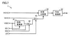
- FIG. 7 is a block diagram showing the main part of the control circuit 7.
- the control circuit 7 receives the output signal VO1D of the voltage detector 6a, the output signal VI1D of the voltage detector 4a, the output signal VI2D of the voltage detector 4b, the selection signals SE1 and SE2, and the abnormality detection signal ⁇ 5.
- the signal VO1D is obtained by dividing the output voltage VO1 of the inverse conversion circuit 3a by the voltage detector 6a, and is a signal that changes in a sinusoidal shape at a commercial frequency.
- the signal VI1D is obtained by dividing the AC voltage VI1 from the commercial AC power supply 51 by the voltage detector 4a, and is a signal that changes in a sine wave shape at the commercial frequency.
- the signal VI2D is obtained by dividing the AC voltage VI2 from the commercial AC power supply 51 by the voltage detector 4b, and is a signal that changes in a sine wave shape at the commercial frequency.
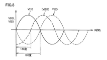
- FIG. 8 is a time chart showing waveforms of the signals VI1D and VI2D. As shown in FIG. 8, the phase of the signal VI2D is delayed by 180 degrees from the phase of the signal VI1D. By advancing the phase of the signal VI2D by 180 degrees, a monitor signal having the same phase as the signal VI1D can be generated.
- phase of the signal VI2D is 180 degrees behind the phase of the signal VI1D.
- the phase of the signal VI2D is 120 degrees behind the phase of the signal VI1D.
- a monitor signal having the same phase as the signal VI1D can be generated by advancing the phase of the signal VI2D by 120 degrees.
- the selection signal SE is set to “H” level in Japan and “L” level in North America.
- the selection signal SE2 is a signal for setting whether or not to perform phase conversion of the signal VI2D. That is, the uninterruptible power supply of the first embodiment can also be used as a single-phase two-wire uninterruptible power supply.
- the input terminals TI1 and TI2 are connected to each other to receive the AC voltage VI1 from the commercial AC power supply 51, and the input terminal TI3 receives the neutral point voltage VN.
- the output terminals TO1 and TO2 are connected to each other and used to output an alternating voltage VO1.
- the load receives AC voltage VO1 from output terminals TO1 and TO2, and receives neutral point voltage VN from output terminal TO3.
- the load includes 100V electrical equipment.
- Selection signal SE2 is set to “H” level when phase conversion of signal VI2D is performed, and is set to “L” level when phase conversion of signal VI2D is not performed.
- the abnormality detection signal ⁇ 5 is set to “H” level when an abnormality occurs in the voltage detector 4a, and is set to “L” level when no abnormality occurs in the voltage detector 4a.
- the control circuit 7 includes a phase conversion unit 41, switching circuits 42 and 43, a phase comparison unit 44, and a PWM control unit 45.
- the phase conversion unit 41 is a monitor in which the phase of the output signal VI2D of the voltage detector 4b is advanced by 180 degrees when the selection signal SE1 is set to “H” level because the uninterruptible power supply is used in Japan.
- the selection signal SE1 is set to "L” level because the signal is generated and the uninterruptible power supply is used in North America, the monitor signal obtained by advancing the phase of the output signal VI2D of the voltage detector 4b by 120 degrees Is generated.
- the switching circuit 42 receives the signal VI2D and the output signal of the phase conversion unit 41, and selects the output signal of the phase conversion unit 41 when the signal SE2 is set to “H” level in order to perform the phase conversion of the signal VI2D.
- the signal SE2 is set to the “L” level because the phase conversion of the signal VI2D is unnecessary, the signal VI2D is selected and supplied to the switching circuit 43.
- the switching circuit 43 provides the signal VI1D to the phase comparison unit 44 when the abnormality detection signal ⁇ 5 is set to “L” level because the voltage detector 4a is normal, and an abnormality has occurred in the voltage detector 4a.
- abnormality detection signal ⁇ 5 is set to “H” level, the signal supplied from switching circuit 42 is applied to phase comparison unit 44.
- the phase comparison unit 44 compares the phase of the signal VO1D with the phase of the signal (for example, the signal VI1D) given from the switching circuit 43, and outputs a signal indicating the comparison result.
- the phase comparison unit 44 has a first zero cross point that becomes 0 V when the signal VO1D changes from a negative voltage to a positive voltage, and a signal (for example, the signal VI1D) given from the switching circuit 43 is a negative voltage.
- the second zero cross point that becomes 0 V when the voltage changes from positive to negative is detected, the phase difference ⁇ (degrees) between the first and second zero cross points is detected, and a signal indicating the detected value is output. .
- the PWM controller 45 Based on the output signal of the phase comparator 44, the PWM controller 45 turns each of the transistors Q5 to Q8 of the inverter 3 on / off so that the phase difference ⁇ between the first and second zero cross points becomes 0 degrees. Adjust the timing.
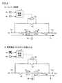
- FIGS. 9A, 9B and 10A, 10B are diagrams schematically showing the operation of the uninterruptible power supply.
- FIGS. 9A, 9B, and 10A, 10B only the portion related to the one-phase AC voltage VI1 is shown for simplification of the drawings and the description. Illustration of the chopper 2 etc. is omitted.
- FIG. 9B when an abnormality occurs in the voltage detector 4a, the operation of the forward conversion circuit 1a is stopped and the switch S1 is turned off, and the reverse conversion circuit 3a, the switch S5, and the output terminal TO1 are connected from the battery 52.
- the current IL flows through the load 53 through the load.
- the control circuit 7 controls the reverse conversion circuit 3a in synchronization with the output signal VI2D of the voltage detector 4b instead of the voltage detector 4a, and changes the phase of the output voltage VO1 of the reverse conversion circuit 3a from the commercial AC power supply 51. To the phase of the AC voltage VI1.
- a signal for turning them on is simultaneously applied to the control electrode of the semiconductor switch S9 and the control electrode of the switch S7, but the response speed of the semiconductor switch S9 is faster than the response speed of the switch S7.
- the switch S7 is turned on. There may be a period in which both the semiconductor switch S9 and the switch S5 are turned on and AC power is supplied from both the commercial AC power supply 51 and the inverse conversion circuit 3a to the load 53.
- the semiconductor switch S9 is turned off after the switch S7 is turned on and the switch S5 is turned off, and the commercial AC power supply 51 is connected to the input terminal TI1, the switch S7, and the output terminal TO1.
- a current IL flows through the load 53.
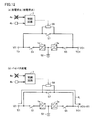
- FIGS. 10 (a) and 10 (b) are diagrams showing a comparative example of the first embodiment, and are compared with FIGS. 10 (a) and 10 (b).
- the output signal VI2D of the voltage detector 4b cannot be used instead of the output signal VI1D of the voltage detector 4a.
- the operation when the voltage detector 4a is normal in the inverter power supply mode is the same as that of the first embodiment, and the switches S1 and S5 are turned on and the switch S7 and the semiconductor switch S9 are turned on.
- the current IL flows from the commercial AC power supply 51 to the load 53 through the input terminal TI1, the switch S1, the forward conversion circuit 1a, the reverse conversion circuit 3a, the switch S5, and the output terminal TO1.
- the control circuit 7 controls the inverse conversion circuit 3a in synchronization with the output signal VI1D of the voltage detector 4a, and changes the phase of the output voltage VO1 of the inverse conversion circuit 3a to the phase of the AC voltage VI1 from the commercial AC power supply 51. Match.
- FIG. 11B when an abnormality occurs in the voltage detector 4a, the operation of the forward conversion circuit 1a is stopped and the switch S1 is turned off, and the reverse conversion circuit 3a, the switch S5, and the output terminal TO1 are connected from the battery 52.
- the current IL flows through the load 53 through the load.
- the control circuit 7 controls the inverse conversion circuit 3a based on the phase information stored before the occurrence of the abnormality. For this reason, the phase of the output voltage VO1 of the inverse conversion circuit 3a cannot be matched with the phase of the AC voltage VI1 from the commercial AC power supply 51.
- the switch S7 is turned on and the switch S5 is turned off, and the current IL flows from the commercial AC power supply 51 to the load 53 through the input terminal TI1, the switch S7, and the output terminal TO1.
- the supply of the two-phase AC power to the load 53 is momentarily interrupted.
- the inverter 3 when the voltage detector 4a becomes abnormal, the inverter 3 is controlled in synchronization with the output signal VI2D of the voltage detector 4b, and the output voltages VO1, VO2 of the inverter 3 are controlled. Are made to coincide with the phases of the AC voltages VI1 and VI2, respectively, and then the semiconductor switches S9 and S10 and the switches S7 and S8 are turned on and the switches S5 and S6 are turned off. Therefore, even when the voltage detector 4a becomes abnormal, the two-phase AC voltage can be supplied to the load 53 without interruption.
- FIG. 13 is a circuit diagram showing a configuration of an input voltage detection circuit 4A included in the uninterruptible power supply according to Embodiment 2 of the present invention, and is a diagram compared with FIG. Referring to FIG. 13, the input voltage detection circuit 4A is different from the input voltage detection circuit 4 of FIG. 3 in that a spare voltage detector 4d and an output terminal T14 are added.
- the voltage detector 4d is connected in series between a plurality of (five in the figure) resistance elements 21 connected in series between the input terminal T1 and the output terminal T14, and between the output terminal T11 and the line of the reference voltage VSS.
- a plurality of (two in the figure) resistance elements 22 are connected to the output terminal T14.
- An AC voltage VI1DA obtained by dividing the AC voltage VI1 at a predetermined voltage dividing ratio appears at the output terminal T14.
- the AC voltage VI1D is the same voltage as the AC voltage VI1D appearing at the output terminal T11.
- the voltages VI1D, VI2D, VND, and VI1DA at the output terminals T11 to T14 are applied to the control circuit 7A as output signals of the voltage detectors 4a to 4d, respectively.
- FIG. 14 is a block diagram showing the main part of the control circuit 7A, which is compared with FIG. Referring to FIG. 14, control circuit 7A differs from control circuit 7 in FIG. 7 in that phase conversion unit 41 and switching circuit 42 are removed.
- the switching circuit 43 receives the output signal VI1D of the voltage detector 4a and the output signal VI1DA of the spare voltage detector 4d. Since the voltage detector 4a is normal, the abnormality detection signal ⁇ 5 is set to the “L” level. The signal VI1D is supplied to the phase comparison unit 44 when the voltage detector 4a is present, and the signal VI1DA is supplied to the phase comparison unit 44 when the abnormality detection signal ⁇ 5 is set to the “H” level due to the occurrence of an abnormality in the voltage detector 4a. Since other configurations and operations are the same as those in the first embodiment, description thereof will not be repeated.
- the inverter 3 when the voltage detector 4a becomes abnormal, the inverter 3 is controlled in synchronization with the output signal VI1DA of the spare voltage detector 4d, and the phases of the output voltages VO1 and VO2 of the inverter 3 are adjusted. After matching the phases of the AC voltages VI1, VI2, respectively, the semiconductor switches S9, S10 and the switches S7, S8 are turned on and the switches S5, S6 are turned off. Therefore, even when the voltage detector 4a becomes abnormal, the two-phase AC voltage can be supplied to the load 53 without interruption.
Landscapes
- Engineering & Computer Science (AREA)
- Power Engineering (AREA)
- Theoretical Computer Science (AREA)
- Physics & Mathematics (AREA)
- General Engineering & Computer Science (AREA)
- General Physics & Mathematics (AREA)
- Business, Economics & Management (AREA)
- Emergency Management (AREA)
- Inverter Devices (AREA)
- Stand-By Power Supply Arrangements (AREA)
- Charge And Discharge Circuits For Batteries Or The Like (AREA)
- Rectifiers (AREA)
Abstract
Description
図1は、この発明の実施の形態1による無停電電源装置の構成を示す回路ブロック図である。図1において、この無停電電源装置は、二相3線式であり、入力端子TI1~TI3、バッテリ端子TB1,TB2、および出力端子TO1~TO3を備える。入力端子TI1~TI3は、商用交流電源51から供給される交流電圧VI1、交流電圧VI2、および中性点電圧VNをそれぞれ受ける。たとえば日本では、交流電圧VI1の位相は、交流電圧VI2の位相よりも180度進んでいる。交流電圧VI1,VI2の各々の実効値は100Vである。中性点電圧VNは、0Vである。
実施の形態1では、電圧検出器4aに異常が発生した場合は、電圧検出器4aの出力信号VI1Dの代わりに電圧検出器4bの出力信号VI2Dを使用してインバータ3を制御した。それに対して本実施の形態2では、予備の電圧検出器4dを設け、電圧検出器4aに異常が発生した場合に、電圧検出器4aの出力信号VI1Dの代わりに予備の電圧検出器4dの出力信号VI1DAを使用してインバータ3を制御する。
Claims (7)
- 二相3線式の無停電電源装置であって、
商用交流電源から供給される二相交流電圧を直流電圧に変換するコンバータと、
前記コンバータによって生成された直流電圧または電力貯蔵装置から供給される直流電圧を二相交流電圧に変換して負荷に供給するインバータと、
一方端子対が前記商用交流電源からの二相交流電圧を受け、他方端子対が前記負荷に接続されたバイパススイッチ対と、
前記バイパススイッチ対に並列接続された半導体スイッチ対と、
それぞれ前記商用交流電源からの二相交流電圧の瞬時値を検出し、検出値を示す信号を出力する第1および第2の電圧検出器と、
前記第1の電圧検出器が正常であるか否かを判定し、判定結果を示す信号を出力する異常検出器と、
前記第1および第2の電圧検出器の出力信号と前記異常検出器の出力信号とに基づいて前記無停電電源装置を制御する制御回路とを備え、
前記制御回路は、
前記第1の電圧検出器が正常である場合は、前記バイパススイッチ対および前記半導体スイッチ対をオフさせるとともに、前記第1の電圧検出器の出力信号に同期して前記コンバータおよび前記インバータを制御し、
前記第1の電圧検出器が異常になった場合は、前記コンバータの運転を停止させるとともに前記第2の電圧検出器の出力信号に同期して前記インバータを制御し、前記電力貯蔵装置の直流電圧を二相交流電圧に変換させるとともにその二相交流電圧の位相を前記商用交流電源からの二相交流電圧の位相に一致させ、前記電力貯蔵装置の端子間電圧が低下して予め定められた電圧に到達したことに応じて前記バイパススイッチ対および前記半導体スイッチ対をオンさせ、予め定められた時間が経過した後に前記半導体スイッチ対をオフさせる、無停電電源装置。 - 前記第1および第2の電圧検出器の出力信号の位相は予め定められた角度だけ互いにずれており、
前記制御回路は、前記第1の電圧検出器が異常になった場合は、前記第2の電圧検出器の出力信号の位相を前記予め定められた角度だけずらせてモニタ信号を生成し、生成したモニタ信号に同期して前記インバータを制御し、前記電力貯蔵装置の直流電圧を二相交流電圧に変換させるとともにその二相交流電圧の位相を前記商用交流電源からの二相交流電圧の位相に一致させる、請求項1に記載の無停電電源装置。 - 前記異常検出器は、前記第1の電圧検出器の出力信号の実効値と前記第2の電圧検出器の出力信号の実効値との差が予め定められたしきい値を超えた場合に前記第1の電圧検出器が異常になったと判定する、請求項1に記載の無停電電源装置。
- 前記制御回路は、前記第2の電圧検出器の出力信号に基づいて、前記商用交流電源からの二相交流電圧の供給が停止されたか否かを判別し、前記商用交流電源からの二相交流電圧の供給が停止されたと判別した場合は、前記コンバータの運転を停止させるとともに前記インバータの運転を継続し、前記電力貯蔵装置の直流電圧を二相交流電圧に変換させる、請求項1に記載の無停電電源装置。
- 二相3線式の無停電電源装置であって、
商用交流電源から供給される二相交流電圧を直流電圧に変換するコンバータと、
前記コンバータによって生成された直流電圧または電力貯蔵装置から供給される直流電圧を二相交流電圧に変換して負荷に供給するインバータと、
一方端子対が前記商用交流電源からの二相交流電圧を受け、他方端子対が前記負荷に接続されたバイパススイッチ対と、
前記バイパススイッチ対に並列接続された半導体スイッチ対と、
各々が、前記商用交流電源からの二相交流電圧のうちの一方の相の交流電圧の瞬時値を検出し、検出値を示す信号を出力する第1および第2の電圧検出器と、
前記商用交流電源からの二相交流電圧のうちの他方の相の交流電圧の瞬時値を検出し、検出値を示す信号を出力する第3の電圧検出器と、
前記第1の電圧検出器が正常であるか否かを判定し、判定結果を示す信号を出力する異常検出器と、
前記第1~第3の電圧検出器の出力信号と前記異常検出器の出力信号とに基づいて前記無停電電源装置を制御する制御回路とを備え、
前記制御回路は、
前記第1の電圧検出器が正常である場合は、前記バイパススイッチ対および前記半導体スイッチ対をオフさせるとともに、前記第1の電圧検出器の出力信号に同期して前記コンバータおよび前記インバータを制御し、
前記第1の電圧検出器が異常になった場合は、前記コンバータの運転を停止させるとともに前記第2の電圧検出器の出力信号に同期して前記インバータを制御し、前記電力貯蔵装置の直流電圧を二相交流電圧に変換させるとともにその二相交流電圧の位相を前記商用交流電源からの二相交流電圧の位相に一致させ、前記電力貯蔵装置の端子間電圧が低下して予め定められた電圧に到達したことに応じて前記バイパススイッチ対および前記半導体スイッチ対をオンさせ、予め定められた時間が経過した後に前記半導体スイッチ対をオフさせる、無停電電源装置。 - 前記異常検出器は、前記第1の電圧検出器の出力信号の実効値と前記第3の電圧検出器の出力信号の実効値との差が予め定められたしきい値を超えた場合に前記第1の電圧検出器が異常になったと判定する、請求項5に記載の無停電電源装置。
- 前記制御回路は、前記第3の電圧検出器の出力信号に基づいて、前記商用交流電源からの二相交流電圧の供給が停止されたか否かを判別し、前記商用交流電源からの二相交流電圧の供給が停止されたと判別した場合は、前記コンバータの運転を停止させるとともに前記インバータの運転を継続し、前記電力貯蔵装置の直流電圧を二相交流電圧に変換させる、請求項5に記載の無停電電源装置。
Priority Applications (5)
| Application Number | Priority Date | Filing Date | Title |
|---|---|---|---|
| JP2017552629A JP6441503B2 (ja) | 2015-11-27 | 2015-11-27 | 無停電電源装置 |
| KR1020187017499A KR102046274B1 (ko) | 2015-11-27 | 2015-11-27 | 무정전 전원 장치 |
| CN201580084788.1A CN108450043B (zh) | 2015-11-27 | 2015-11-27 | 不间断电源装置 |
| US15/772,163 US10756567B2 (en) | 2015-11-27 | 2015-11-27 | Uninterruptible power supply device |
| PCT/JP2015/083357 WO2017090174A1 (ja) | 2015-11-27 | 2015-11-27 | 無停電電源装置 |
Applications Claiming Priority (1)
| Application Number | Priority Date | Filing Date | Title |
|---|---|---|---|
| PCT/JP2015/083357 WO2017090174A1 (ja) | 2015-11-27 | 2015-11-27 | 無停電電源装置 |
Publications (1)
| Publication Number | Publication Date |
|---|---|
| WO2017090174A1 true WO2017090174A1 (ja) | 2017-06-01 |
Family
ID=58763270
Family Applications (1)
| Application Number | Title | Priority Date | Filing Date |
|---|---|---|---|
| PCT/JP2015/083357 Ceased WO2017090174A1 (ja) | 2015-11-27 | 2015-11-27 | 無停電電源装置 |
Country Status (5)
| Country | Link |
|---|---|
| US (1) | US10756567B2 (ja) |
| JP (1) | JP6441503B2 (ja) |
| KR (1) | KR102046274B1 (ja) |
| CN (1) | CN108450043B (ja) |
| WO (1) | WO2017090174A1 (ja) |
Cited By (2)
| Publication number | Priority date | Publication date | Assignee | Title |
|---|---|---|---|---|
| JP2020005479A (ja) * | 2018-07-02 | 2020-01-09 | サンケン電気株式会社 | 三相電力変換装置及び無停電電源装置 |
| JP2024168550A (ja) * | 2023-05-24 | 2024-12-05 | 株式会社Tmeic | 無停電電源装置 |
Families Citing this family (13)
| Publication number | Priority date | Publication date | Assignee | Title |
|---|---|---|---|---|
| JP6725647B2 (ja) * | 2016-04-14 | 2020-07-22 | 東芝三菱電機産業システム株式会社 | 無停電電源装置 |
| WO2020105135A1 (ja) * | 2018-11-21 | 2020-05-28 | 東芝三菱電機産業システム株式会社 | 電源装置 |
| WO2020240761A1 (ja) * | 2019-05-30 | 2020-12-03 | 東芝三菱電機産業システム株式会社 | 無停電電源装置 |
| US11336114B2 (en) * | 2019-06-25 | 2022-05-17 | Toshiba Mitsubishi-Electric Industrial Systems Corporation | Uninterruptible power supply apparatus |
| CN113169660B (zh) * | 2019-07-04 | 2024-03-08 | 东芝三菱电机产业系统株式会社 | 同步控制电路及具备同步控制电路的不间断电源装置 |
| KR102077528B1 (ko) * | 2019-07-11 | 2020-02-14 | 아이에프텍(주) | Iot 기반의 무정전 전원 공급 장치의 연결 구조 및 그 제어 방법 |
| KR102276024B1 (ko) * | 2019-10-30 | 2021-07-12 | 엘에스일렉트릭(주) | 무순단 전원 공급 제어 장치 및 그 전원 공급 제어 장치가 적용된 ups 모듈 |
| WO2021220704A1 (ja) * | 2020-04-28 | 2021-11-04 | 工機ホールディングス株式会社 | 作業機 |
| CN111900885A (zh) * | 2020-07-15 | 2020-11-06 | 国网北京市电力公司 | 台区识别测试装置的供电电源的控制方法及装置 |
| CN114069817A (zh) * | 2020-07-31 | 2022-02-18 | 华为数字能源技术有限公司 | 一种不间断电源、通断控制模块、控制方法及系统 |
| JP7200398B1 (ja) * | 2021-04-16 | 2023-01-06 | 東芝三菱電機産業システム株式会社 | 無停電電源装置 |
| CN115642685A (zh) * | 2022-10-20 | 2023-01-24 | 华为数字能源技术有限公司 | 不间断电源系统的控制方法、控制器及不间断电源系统 |
| US12278626B2 (en) * | 2023-08-11 | 2025-04-15 | Infineon Technologies Ag | Driver circuit for bypass power transistor including secondary supply input connection from a power delivery circuit |
Citations (2)
| Publication number | Priority date | Publication date | Assignee | Title |
|---|---|---|---|---|
| JPH06253549A (ja) * | 1993-02-26 | 1994-09-09 | Toshiba Corp | 無停電電源装置 |
| JP2004135370A (ja) * | 2002-10-08 | 2004-04-30 | Kawasaki Heavy Ind Ltd | 無停電電源装置及び電力供給方法 |
Family Cites Families (12)
| Publication number | Priority date | Publication date | Assignee | Title |
|---|---|---|---|---|
| JP2004015919A (ja) | 2002-06-07 | 2004-01-15 | Mitsubishi Electric Corp | 無停電電源装置 |
| JP4407808B2 (ja) | 2004-03-31 | 2010-02-03 | サンケン電気株式会社 | 電源装置 |
| JP2007300712A (ja) * | 2006-04-28 | 2007-11-15 | Sanken Electric Co Ltd | 交流電力供給装置 |
| JP4669860B2 (ja) * | 2007-07-06 | 2011-04-13 | 三菱電機株式会社 | 無停電電源装置 |
| JP2009303419A (ja) * | 2008-06-16 | 2009-12-24 | Toshiba Mitsubishi-Electric Industrial System Corp | 無停電電源システム |
| JP2010115008A (ja) * | 2008-11-06 | 2010-05-20 | Tdk-Lambda Corp | 無停電電源装置 |
| CA2763646C (en) * | 2009-05-29 | 2015-11-17 | Toshiba Mitsubishi-Electric Industrial Systems Corporation | Uninterruptible power supply device |
| US9093861B2 (en) * | 2009-09-16 | 2015-07-28 | Toshiba Mitsubishi-Electric Industrial Systems Corporation | Power conversion system and uninterruptible power supply system |
| CN102856935B (zh) * | 2011-06-29 | 2015-06-03 | 力博特公司 | Ups系统及其在eco模式下为非线性负载供电的方法 |
| CN203554063U (zh) * | 2013-11-29 | 2014-04-16 | 天津铁路信号有限责任公司 | 铁路道口信号设备用电源柜 |
| CN103683476A (zh) * | 2013-12-19 | 2014-03-26 | 重庆市星海电子有限公司 | 车载综合移动不间断电源供给装置 |
| JP6208326B2 (ja) * | 2014-03-10 | 2017-10-04 | 株式会社日立製作所 | 電力変換ユニット、電力変換装置、および電力変換方法 |
-
2015
- 2015-11-27 US US15/772,163 patent/US10756567B2/en active Active
- 2015-11-27 CN CN201580084788.1A patent/CN108450043B/zh active Active
- 2015-11-27 WO PCT/JP2015/083357 patent/WO2017090174A1/ja not_active Ceased
- 2015-11-27 KR KR1020187017499A patent/KR102046274B1/ko active Active
- 2015-11-27 JP JP2017552629A patent/JP6441503B2/ja active Active
Patent Citations (2)
| Publication number | Priority date | Publication date | Assignee | Title |
|---|---|---|---|---|
| JPH06253549A (ja) * | 1993-02-26 | 1994-09-09 | Toshiba Corp | 無停電電源装置 |
| JP2004135370A (ja) * | 2002-10-08 | 2004-04-30 | Kawasaki Heavy Ind Ltd | 無停電電源装置及び電力供給方法 |
Cited By (4)
| Publication number | Priority date | Publication date | Assignee | Title |
|---|---|---|---|---|
| JP2020005479A (ja) * | 2018-07-02 | 2020-01-09 | サンケン電気株式会社 | 三相電力変換装置及び無停電電源装置 |
| JP7175649B2 (ja) | 2018-07-02 | 2022-11-21 | 株式会社Gsユアサ インフラシステムズ | 三相電力変換装置及び無停電電源装置 |
| JP2024168550A (ja) * | 2023-05-24 | 2024-12-05 | 株式会社Tmeic | 無停電電源装置 |
| JP7822995B2 (ja) | 2023-05-24 | 2026-03-03 | 株式会社Tmeic | 無停電電源装置 |
Also Published As
| Publication number | Publication date |
|---|---|
| CN108450043B (zh) | 2021-06-08 |
| CN108450043A (zh) | 2018-08-24 |
| US10756567B2 (en) | 2020-08-25 |
| KR20180083931A (ko) | 2018-07-23 |
| JPWO2017090174A1 (ja) | 2018-08-30 |
| JP6441503B2 (ja) | 2018-12-19 |
| KR102046274B1 (ko) | 2019-11-18 |
| US20180316216A1 (en) | 2018-11-01 |
Similar Documents
| Publication | Publication Date | Title |
|---|---|---|
| JP6441503B2 (ja) | 無停電電源装置 | |
| CN107836068B (zh) | 不间断电源装置 | |
| US9882508B2 (en) | High-frequency switching type conversion device | |
| EP1852963B1 (en) | Power conversion apparatus | |
| EP3171503B1 (en) | Cascaded multilevel converter self-test system and self-test method for the same | |
| US10615636B2 (en) | Uninterruptible power supply | |
| US11056907B2 (en) | Uninterruptible power supply device | |
| US11196292B2 (en) | Uninterruptible power supply system | |
| US10263558B2 (en) | Phase loss detection in active front end converters | |
| TWI623174B (zh) | 不斷電電源裝置 | |
| US9780681B2 (en) | Power conversion system including plurality of power converters connected in parallel to load | |
| US11394295B2 (en) | Power supply apparatus | |
| US11005384B2 (en) | Power conversion device | |
| CN111480280A (zh) | 电力转换系统 | |
| US20220385204A1 (en) | Power Conversion Device and Press Apparatus | |
| JP6789197B2 (ja) | 電力変換装置 | |
| US11196290B2 (en) | Uninterruptible power supply apparatus | |
| EP2953251B1 (en) | Power conversion device | |
| JP6668556B2 (ja) | 電源装置およびそれを用いた電源システム | |
| JP6749862B2 (ja) | 直列多重インバータ装置 | |
| JP4893113B2 (ja) | 整流回路の制御装置 | |
| JP5978926B2 (ja) | 5レベル電力変換器 | |
| CN111989853B (zh) | 电力变换装置 | |
| JP5481055B2 (ja) | 電力変換装置 | |
| JP6034143B2 (ja) | 電力変換装置 |
Legal Events
| Date | Code | Title | Description |
|---|---|---|---|
| 121 | Ep: the epo has been informed by wipo that ep was designated in this application |
Ref document number: 15909291 Country of ref document: EP Kind code of ref document: A1 |
|
| ENP | Entry into the national phase |
Ref document number: 2017552629 Country of ref document: JP Kind code of ref document: A |
|
| WWE | Wipo information: entry into national phase |
Ref document number: 15772163 Country of ref document: US |
|
| NENP | Non-entry into the national phase |
Ref country code: DE |
|
| ENP | Entry into the national phase |
Ref document number: 20187017499 Country of ref document: KR Kind code of ref document: A |
|
| WWE | Wipo information: entry into national phase |
Ref document number: 1020187017499 Country of ref document: KR |
|
| 122 | Ep: pct application non-entry in european phase |
Ref document number: 15909291 Country of ref document: EP Kind code of ref document: A1 |