WO2017085871A1 - 給電回路及びアンテナ装置 - Google Patents
給電回路及びアンテナ装置 Download PDFInfo
- Publication number
- WO2017085871A1 WO2017085871A1 PCT/JP2015/082731 JP2015082731W WO2017085871A1 WO 2017085871 A1 WO2017085871 A1 WO 2017085871A1 JP 2015082731 W JP2015082731 W JP 2015082731W WO 2017085871 A1 WO2017085871 A1 WO 2017085871A1
- Authority
- WO
- WIPO (PCT)
- Prior art keywords
- power
- output
- circuit
- antenna
- antenna elements
- Prior art date
- Legal status (The legal status is an assumption and is not a legal conclusion. Google has not performed a legal analysis and makes no representation as to the accuracy of the status listed.)
- Ceased
Links
Images






Classifications
-
- H—ELECTRICITY
- H01—ELECTRIC ELEMENTS
- H01Q—ANTENNAS, i.e. RADIO AERIALS
- H01Q3/00—Arrangements for changing or varying the orientation or the shape of the directional pattern of the waves radiated from an antenna or antenna system
- H01Q3/26—Arrangements for changing or varying the orientation or the shape of the directional pattern of the waves radiated from an antenna or antenna system varying the relative phase or relative amplitude of energisation between two or more active radiating elements; varying the distribution of energy across a radiating aperture
- H01Q3/28—Arrangements for changing or varying the orientation or the shape of the directional pattern of the waves radiated from an antenna or antenna system varying the relative phase or relative amplitude of energisation between two or more active radiating elements; varying the distribution of energy across a radiating aperture varying the amplitude
-
- H—ELECTRICITY
- H01—ELECTRIC ELEMENTS
- H01Q—ANTENNAS, i.e. RADIO AERIALS
- H01Q3/00—Arrangements for changing or varying the orientation or the shape of the directional pattern of the waves radiated from an antenna or antenna system
- H01Q3/26—Arrangements for changing or varying the orientation or the shape of the directional pattern of the waves radiated from an antenna or antenna system varying the relative phase or relative amplitude of energisation between two or more active radiating elements; varying the distribution of energy across a radiating aperture
-
- H—ELECTRICITY
- H01—ELECTRIC ELEMENTS
- H01Q—ANTENNAS, i.e. RADIO AERIALS
- H01Q21/00—Antenna arrays or systems
- H01Q21/06—Arrays of individually energised antenna units similarly polarised and spaced apart
- H01Q21/061—Two dimensional planar arrays
- H01Q21/065—Patch antenna array
-
- H—ELECTRICITY
- H01—ELECTRIC ELEMENTS
- H01Q—ANTENNAS, i.e. RADIO AERIALS
- H01Q21/00—Antenna arrays or systems
- H01Q21/06—Arrays of individually energised antenna units similarly polarised and spaced apart
- H01Q21/22—Antenna units of the array energised non-uniformly in amplitude or phase, e.g. tapered array or binomial array
-
- H—ELECTRICITY
- H01—ELECTRIC ELEMENTS
- H01Q—ANTENNAS, i.e. RADIO AERIALS
- H01Q21/00—Antenna arrays or systems
- H01Q21/24—Combinations of antenna units polarised in different directions for transmitting or receiving circularly and elliptically polarised waves or waves linearly polarised in any direction
- H01Q21/245—Combinations of antenna units polarised in different directions for transmitting or receiving circularly and elliptically polarised waves or waves linearly polarised in any direction provided with means for varying the polarisation
-
- H—ELECTRICITY
- H01—ELECTRIC ELEMENTS
- H01Q—ANTENNAS, i.e. RADIO AERIALS
- H01Q21/00—Antenna arrays or systems
- H01Q21/28—Combinations of substantially independent non-interacting antenna units or systems
-
- H—ELECTRICITY
- H01—ELECTRIC ELEMENTS
- H01Q—ANTENNAS, i.e. RADIO AERIALS
- H01Q25/00—Antennas or antenna systems providing at least two radiating patterns
-
- H—ELECTRICITY
- H01—ELECTRIC ELEMENTS
- H01Q—ANTENNAS, i.e. RADIO AERIALS
- H01Q3/00—Arrangements for changing or varying the orientation or the shape of the directional pattern of the waves radiated from an antenna or antenna system
- H01Q3/26—Arrangements for changing or varying the orientation or the shape of the directional pattern of the waves radiated from an antenna or antenna system varying the relative phase or relative amplitude of energisation between two or more active radiating elements; varying the distribution of energy across a radiating aperture
- H01Q3/30—Arrangements for changing or varying the orientation or the shape of the directional pattern of the waves radiated from an antenna or antenna system varying the relative phase or relative amplitude of energisation between two or more active radiating elements; varying the distribution of energy across a radiating aperture varying the relative phase between the radiating elements of an array
- H01Q3/34—Arrangements for changing or varying the orientation or the shape of the directional pattern of the waves radiated from an antenna or antenna system varying the relative phase or relative amplitude of energisation between two or more active radiating elements; varying the distribution of energy across a radiating aperture varying the relative phase between the radiating elements of an array by electrical means
-
- H—ELECTRICITY
- H04—ELECTRIC COMMUNICATION TECHNIQUE
- H04B—TRANSMISSION
- H04B7/00—Radio transmission systems, i.e. using radiation field
- H04B7/02—Diversity systems; Multi-antenna system, i.e. transmission or reception using multiple antennas
- H04B7/04—Diversity systems; Multi-antenna system, i.e. transmission or reception using multiple antennas using two or more spaced independent antennas
- H04B7/06—Diversity systems; Multi-antenna system, i.e. transmission or reception using multiple antennas using two or more spaced independent antennas at the transmitting station
- H04B7/0613—Diversity systems; Multi-antenna system, i.e. transmission or reception using multiple antennas using two or more spaced independent antennas at the transmitting station using simultaneous transmission
- H04B7/0615—Diversity systems; Multi-antenna system, i.e. transmission or reception using multiple antennas using two or more spaced independent antennas at the transmitting station using simultaneous transmission of weighted versions of same signal
- H04B7/0617—Diversity systems; Multi-antenna system, i.e. transmission or reception using multiple antennas using two or more spaced independent antennas at the transmitting station using simultaneous transmission of weighted versions of same signal for beam forming
-
- H—ELECTRICITY
- H04—ELECTRIC COMMUNICATION TECHNIQUE
- H04B—TRANSMISSION
- H04B7/00—Radio transmission systems, i.e. using radiation field
- H04B7/02—Diversity systems; Multi-antenna system, i.e. transmission or reception using multiple antennas
- H04B7/04—Diversity systems; Multi-antenna system, i.e. transmission or reception using multiple antennas using two or more spaced independent antennas
- H04B7/06—Diversity systems; Multi-antenna system, i.e. transmission or reception using multiple antennas using two or more spaced independent antennas at the transmitting station
- H04B7/0613—Diversity systems; Multi-antenna system, i.e. transmission or reception using multiple antennas using two or more spaced independent antennas at the transmitting station using simultaneous transmission
- H04B7/0667—Diversity systems; Multi-antenna system, i.e. transmission or reception using multiple antennas using two or more spaced independent antennas at the transmitting station using simultaneous transmission of delayed versions of same signal
- H04B7/0671—Diversity systems; Multi-antenna system, i.e. transmission or reception using multiple antennas using two or more spaced independent antennas at the transmitting station using simultaneous transmission of delayed versions of same signal using different delays between antennas
-
- H—ELECTRICITY
- H01—ELECTRIC ELEMENTS
- H01Q—ANTENNAS, i.e. RADIO AERIALS
- H01Q1/00—Details of, or arrangements associated with, antennas
- H01Q1/12—Supports; Mounting means
- H01Q1/22—Supports; Mounting means by structural association with other equipment or articles
- H01Q1/24—Supports; Mounting means by structural association with other equipment or articles with receiving set
- H01Q1/241—Supports; Mounting means by structural association with other equipment or articles with receiving set used in mobile communications, e.g. GSM
- H01Q1/246—Supports; Mounting means by structural association with other equipment or articles with receiving set used in mobile communications, e.g. GSM specially adapted for base stations
-
- H—ELECTRICITY
- H01—ELECTRIC ELEMENTS
- H01Q—ANTENNAS, i.e. RADIO AERIALS
- H01Q21/00—Antenna arrays or systems
- H01Q21/06—Arrays of individually energised antenna units similarly polarised and spaced apart
- H01Q21/20—Arrays of individually energised antenna units similarly polarised and spaced apart the units being spaced along or adjacent to a curvilinear path
- H01Q21/205—Arrays of individually energised antenna units similarly polarised and spaced apart the units being spaced along or adjacent to a curvilinear path providing an omnidirectional coverage
Definitions
- the present invention relates to a feeding circuit and an antenna device for a dual beam antenna.
- dual beam antennas also referred to as twin beam antennas
- twin beam antennas that radiate two beams in different directions using a plurality of common antenna elements arranged in the horizontal direction.
- the power supply circuit for the dual beam antenna has two power supply terminals to which power supply signals are input, distributes the power supply signals input from the two power supply terminals to each antenna element, and supplies power to each antenna element.
- the radiation directions and the like of the two beams are adjusted by adjusting the power and phase of the signal, respectively.
- Patent Documents 1 and 2 disclose a power supply circuit configuration in the case where three, four, or six antenna elements are arranged in the horizontal direction.
- the communication area is divided into a plurality of sectors to improve the capacity and the communication speed.
- a communication area is divided every 60 degrees in a horizontal plane to form 6 sectors.
- An antenna device used for a 6-sector base station has a full width at half maximum of a radiated beam of about 33 degrees, and requires low sidelobe directivity in a horizontal plane so as not to affect communication in other sectors.
- an object of the present invention is to provide a feeding circuit and an antenna apparatus for a dual beam antenna that can easily realize a full width at half maximum suitable for a 6-sector base station and has a simple structure.
- the present invention is a power feeding circuit that feeds power to first to fifth antenna elements sequentially arranged in a horizontal direction, and includes two input terminals to which power feeding signals are input, Two output ends, and the power input from the two input ends is equally distributed to be output from the two output ends, and the feeding signal input from one of the input ends is The phase is delayed by 90 degrees with respect to the output end, and the output is output to the other output end, and the feeding signal input from the other input end is delayed by 90 degrees with respect to the other output end.
- a 90-degree hybrid circuit that outputs to the output terminal, an equal distribution circuit that equally distributes the feed signal output from one of the output terminals and outputs the same to the second and fourth antenna elements, and the other output terminal
- the power supply signal output from And a distribution circuit that outputs to the first, third, and fifth antenna elements, and the distribution circuit has the same power output to the first and fifth antenna elements, and the first and The sum of the power output to the five antenna elements is distributed so as to be less than or equal to the power output to the third antenna element, and the third antenna element, the second antenna element, and the fourth antenna element
- a power feeding circuit configured to feed power to either one with the phase reversed.
- the present invention includes first to fifth antenna elements sequentially arranged in a horizontal direction, and a power feeding circuit that feeds power to each of the antenna elements.
- a power feeding circuit that feeds power to each of the antenna elements.
- the power supply signal input from the input terminal is output to the other output terminal with a phase delayed by 90 degrees with respect to one of the output terminals
- the power supply signal input from the other input terminal is A 90-degree hybrid circuit that delays the phase by 90 degrees with respect to the output terminal and outputs it to one of the output terminals, and the second and fourth antennas by equally distributing the feeding signal output from one of the output terminals
- Equal distribution circuit that outputs to the element
- a distribution circuit that distributes the power feeding signal output from the other output end and outputs the power supply signal to the first, third, and fifth antenna elements, and the distribution circuit includes the first and fifth antenna elements.
- the third antenna element is distributed so that the sum of the power output to the first and fifth antenna elements is equal to or less than the power output to the third antenna element.
- an antenna device configured to feed power with a phase inverted to one of the second antenna element and the fourth antenna element.
- the present invention it is possible to easily provide a full width at half maximum suitable for a 6-sector base station, and to provide a feeding circuit and an antenna device for a dual beam antenna with a simple structure.
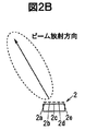
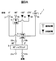
- FIG. 1 is a schematic configuration diagram schematically illustrating an antenna device according to an embodiment of the present invention. It is sectional drawing which shows schematic structure of an antenna element. It is explanatory drawing which shows the relationship between the slot element in an antenna element, and a feed line. It is explanatory drawing explaining normal electric power feeding of a 1st slot element. It is explanatory drawing explaining the inversion electric power feeding of a 1st slot element. It is explanatory drawing explaining the 6 sector base station using an antenna apparatus. It is a graph which shows the radiation characteristic of an antenna apparatus.
- FIG. 1 is a schematic configuration diagram schematically showing a power feeding circuit according to the present embodiment.
- the present inventors diligently studied an antenna device capable of realizing a full width at half maximum of about 33 degrees (more specifically, 30 to 33 degrees ⁇ 5 degrees) suitable for a 6-sector base station. It has been found that the full width at half maximum suitable for a 6-sector base station can be easily realized by setting the number of antenna elements to 5 and devising the circuit configuration of the feeder circuit.
- a power feeding circuit 1 is a circuit that feeds power to five antenna elements 2 arranged in the horizontal direction.
- the first to fifth antenna elements 2a to 2e are sequentially arranged in the horizontal direction.
- a specific configuration of the antenna device equipped with the power feeding circuit 1 will be described later.
- the power feeding circuit 1 includes a 90-degree hybrid circuit 3, an equal distribution circuit 4, and an unequal distribution circuit 5.
- the 90 degree hybrid circuit (also referred to as 90 degree 3 dB hybrid circuit) 3 has two input terminals 31a and 31b to which a power feeding signal is input and two output terminals 32a and 32b.
- the 90-degree hybrid circuit 3 is configured to equally distribute the power input from the two input terminals 31a and 31b and output the power from the two output terminals 32a and 32b.
- the 90-degree hybrid circuit 3 outputs a power feeding signal input from one input end 31a to the other output end 32b with a phase delayed by 90 degrees with respect to the one output end 32a, and the other input
- the power supply signal input from the end 31b is configured to be output to one output end 32a with a phase delayed by 90 degrees with respect to the other output end 32b.
- One output end 32 a of the 90-degree hybrid circuit 3 is electrically connected to the input of the equal distribution circuit 4.
- the other output end 32 b of the 90-degree hybrid circuit 3 is electrically connected to the input of the unequal distribution circuit 5. Note that the specific configuration of the 90-degree hybrid circuit 3 is well-known, and a description thereof will be omitted here.
- the equal distribution circuit 4 is configured to equally distribute the power feeding signal output from one output end 32a of the 90-degree hybrid circuit 3 and output it to the second and fourth antenna elements 2b and 2d.
- One output of the equal distribution circuit 4 is electrically connected to the second antenna element 2b, and the other output is electrically connected to the fourth antenna element 2d.
- the unequal distribution circuit 5 is composed of a 1-input 3-output distribution circuit, and distributes the feeding signal output from the other output end 32b of the 90-degree hybrid circuit 3 to distribute the first, third, and fifth antenna elements 2a, It is configured to output to 2c, 2e.
- the unequal distribution circuit 5 has the same power output to the first and fifth antenna elements 2a and 2e, and the sum of the power output to the first and fifth antenna elements 2a and 2e is the third antenna element.
- the power is distributed so as to be less than or equal to the power output to 2c.
- the equal distribution circuit 4, the unequal distribution circuit 5, the wiring between the circuits 3, 4, 5 and the wiring between the distribution circuits 4, 5 and each antenna element 2 are configured by microstrip lines using a printed circuit board. May be. Moreover, each circuit 3, 4, 5 and the antenna element 2 may be mounted on a common printed circuit board and integrated.
- the power feeding circuit 1 is configured to feed power with the phase inverted to the third antenna element 2c and the fourth antenna element 2d.
- the third antenna element 2c and the fourth antenna element 2d are configured to be fed by inverting feeding to invert the phase. Details of the reverse power feeding will be described later.
- the present invention is not limited to inverting feeding, and for example, a phase adjusting circuit such as a delay circuit may be inserted so that the third antenna element 2c and the fourth antenna element 2d are fed with their phases reversed.
- a phase adjusting circuit such as a delay circuit may be inserted so that the third antenna element 2c and the fourth antenna element 2d are fed with their phases reversed.
- the phase adjusted by the phase adjustment circuit may change depending on the frequency of the power supply signal. It is more desirable to use it.
- the power output from the output terminals 32a and 32b of the 90-degree hybrid circuit 3 is P1 + P2, and the power of (P1 + P2) / 2 is fed to the second and fourth antenna elements 2b and 2d. .
- the feeding power is larger for the antenna element arranged at the center, and the feeding power is smaller for the antenna element arranged at the end, thereby suppressing unnecessary radiation and reducing side lobes. It is known that it can be suppressed.
- the ratio of P1 and P2 can be easily adjusted by the unequal distribution circuit 5, and the ratio of power supplied to each antenna element 2 can be easily adjusted to suppress side lobes. is there.
- the phase of the power feeding signal fed to the first and fifth antenna elements 2a and 2e is ⁇ 90 degrees, which is the same as the phase of the power feeding signal outputted from the other output end 32b.
- the phase of the power feeding signal fed to the second antenna element 2b is 0 degrees, which is the same as the phase of the power feeding signal output from the one output end 32a.
- the phase of the power feeding signal fed to the third antenna element 2c is 90 degrees, which is the phase of the power feeding signal outputted from the other output end 32b. Further, the phase of the power feeding signal fed to the fourth antenna element 2d is obtained by inverting the phase of the power feeding signal outputted from the one output end 32a, and becomes 180 degrees.
- the phases of the first to fifth antenna elements 2a to 2e are -90 degrees, 0 degrees, 90 degrees, 180 degrees, and -90 degrees (270), respectively.
- feed signals having phases different from each other by 90 degrees are supplied to each antenna element 2.
- the beam is emitted in the direction on the left side of the drawing.
- the phase of the power feeding signal fed to the first and fifth antenna elements 2a and 2e is 0 degrees, which is the same as the phase of the feeding signal outputted from the other output end 32b. Further, the phase of the power feeding signal fed to the second antenna element 2b is ⁇ 90 degrees, which is the same as the phase of the power feeding signal outputted from the one output end 32a.
- the phase of the power feeding signal fed to the third antenna element 2c is an inversion of the phase of the power feeding signal outputted from the other output end 32b, and is ⁇ 180 degrees (180 degrees). Further, the phase of the power feeding signal fed to the fourth antenna element 2d is obtained by inverting the phase of the power feeding signal outputted from the one output end 32a, and is -270 degrees (90 degrees).
- the phases of the first to fifth antenna elements 2a to 2e are 0 degree, ⁇ 90 degrees, ⁇ 180 degrees, ⁇ 270 degrees, and 0 degrees, respectively. ⁇ 360 degrees), and feeding signals having phases different from each other by 90 degrees are supplied to each antenna element 2.
- the beam is emitted in the right direction in the figure.
- the radiation direction of the beam can be adjusted by the distance between the antenna elements 2.
- the distance between the antenna elements 2 is set so that the angle formed in the horizontal plane between the radiation directions of the two beams output when power is supplied from both input ends 31a and 31b is about 60 degrees. It is good to adjust.
- the inverting feed is performed on the third and fourth antenna elements 2c and 2d.
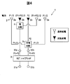
- the present invention is not limited to this, and the inverting feed is applied to the second and third antenna elements 2b and 2c as shown in FIG. It may be configured to do.
- the beam is radiated in the direction on the left side of the figure, and when a feed signal is input from the input end 31b on the left side of the figure, the beam is emitted in the direction on the right side of the figure.
- the radiation direction of the beam is opposite to that in FIG.
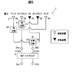
- the unequal distribution circuit 5 having one input and three outputs may be composed of two distribution circuits, ie, an unequal distribution circuit 51 having one input and two outputs and an equal distribution circuit 52.
- the unequal distribution circuit 51 is configured to output the power of P2 to the third antenna element 2c and output the power of P1 (P1 ⁇ P2, preferably P1 ⁇ P2) to the equal distribution circuit 52.
- the equal distribution circuit 52 is configured to equally distribute the input P1 power and output it to the first and fifth antenna elements 2a and 2e.
- the distribution circuits 51 and 52 are connected in multiple stages, and therefore, when applied to an antenna device having a wide use frequency range, each antenna element at a specific frequency due to the influence of reflection or the like. It is also conceivable that the power distribution ratio to 2 deviates from a desired value. In addition, if the distribution circuits 51 and 52 are connected in multiple stages, the circuit may be increased in size. Therefore, it can be said that it is more desirable to use the unequal distribution circuit 5 having one input and three outputs as shown in FIG.
- FIG. 6A is a schematic configuration diagram showing an arrangement of antenna elements of the antenna device
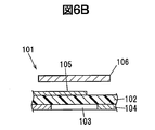
- FIG. 6B is a cross-sectional view showing a schematic configuration of the antenna elements
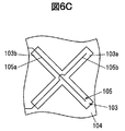
- FIG. 6C is an explanatory diagram showing a relationship between the slots and the feed lines.
- the antenna device 100 is configured by arranging antenna elements 101 in the horizontal direction (left-right direction in the figure) and the vertical direction (up-down direction in the figure).
- the antenna elements 101 are arranged in the horizontal direction.
- the number of arrangement in the vertical direction (number of stages) can be set as appropriate, for example, 12 stages, 16 stages, and the like.
- each antenna element 101 is composed of a slot-coupled patch antenna.
- the antenna element 101 is composed of a conductor layer formed on the back surface of the dielectric substrate 102, a slot forming layer 104 in which a slot 103 penetrating the conductor layer is formed, and a power feeding element formed on the surface of the dielectric substrate 102. It has a feed line 105 and a rectangular plate-shaped radiating element 106 that is disposed facing and spaced from the surface of the dielectric substrate 102.
- the shape of the slot 103 is formed in an X shape, and the first slot element 103a inclined 45 degrees with respect to the vertical direction, and the second slot element 103b inclined ⁇ 45 degrees with respect to the vertical direction, , Formed.
- the feed line 105 includes a first feed line 105a that feeds power to the first slot element 103a and a second feed line 105b that feeds power to the second slot element 103b.
- the first feed line 105a is formed so as to cross the first slot element 103a in the minor axis direction in a plan view at the center position in the major axis direction of the first slot element 103a.
- the first slot element 103a is excited and coupled to the radiating element 106 to radiate radio waves.
- the radio wave radiated at this time is polarized with an inclination of 45 degrees with respect to the vertical direction.
- the second feed line 105b is formed so as to cross the second slot element 103b in the minor axis direction in plan view at the center position in the major axis direction of the second slot element 103b.
- the second slot element 103b is excited and coupled to the radiating element 106 to radiate radio waves.
- the radio wave radiated at this time is polarized with an inclination of ⁇ 45 degrees with respect to the vertical direction.
- the five first slot elements 103a arranged in the horizontal direction correspond to the first to fifth antenna elements 2a to 2e in FIG. 1, and the five first slot elements 103a are included in the present embodiment.
- the power feeding circuit 1 according to is connected.
- the first slot elements 103a corresponding to the third and fourth antenna elements 2c and 2d (first slot elements 103a of the third and fourth antenna elements 101 from the left in FIG. 6A). ) Is reversely fed.
- the normal feeding of the first slot element 103a has a structure in which the first feeding line 105a extends from the upper left to the lower right and intersects the first slot element 103a as shown in FIG. 7A.
- the first feed line 105a extends from the lower right to the upper left and intersects the first slot element 103a, so that the direction of the current of the feed signal is opposite to that in FIG. 7A. Inversion power feeding can be realized.
- the five second slot elements 103b arranged in the horizontal direction correspond to the first to fifth antenna elements 2a to 2e in FIG. 1, and the five first slot elements 103a are connected to the first slot element 103a.
- the power feeding circuit 1 according to the embodiment is connected.
- the second slot elements 103b corresponding to the third and fourth antenna elements 2c and 2d are configured to be fed in an inverted manner.
- the five slot elements 103a and 103b arranged in the horizontal direction are each treated as one set, and the feed circuit 1 is connected to each set of the slot elements 103a and 103b. Yes.
- each power feeding circuit 1 the power and phase of the power feeding signal are distributed to each set of antenna elements 101 arranged in the vertical direction and supplied to each set of antenna elements 101.
- An upstream power supply circuit is provided for adjusting the power. By adjusting the power and phase of the feed signal supplied to each set of antenna elements 101 by this upstream feed circuit, the beam radiation direction in the vertical direction, that is, the electrical tilt angle can be adjusted.
- the antenna device 100 is a dual beam antenna that can radiate beams in two directions, and can cover two sectors. Therefore, by using three antenna devices 100 as shown in FIG. An antenna device can be easily realized. In FIG. 8, the range in which the beam is radiated is schematically shown by broken lines.
- the radiation characteristics of the antenna device 100 are shown in FIG. 9, the left beam is emitted when a power feed signal is input from the left input end 31a in FIG. 1, and the beam emitted when a feed signal is input from the right input end 31b in FIG. Shown as a beam.
- the side lobes of both the left and right beams are as low as ⁇ 20 dB or less, and the 3 dB beam width (full width at half maximum) is about 30 degrees. It is suitable as a device.
- the power feeding circuit 1 is configured to feed power to the first to fifth antenna elements 2a to 2e that are sequentially arranged in the horizontal direction, and a feed signal is input 2
- a feed signal is input 2
- the power supply signal input from the input end 31a is output to the other output end 32b with a phase delayed by 90 degrees with respect to the one output end 32a, and the power supply signal input from the other input end 31b is
- the 90-degree hybrid circuit 3 that delays the phase by 90 degrees with respect to the other output end 32b and outputs it to the one output end 32a, and the power supply signal output from the one output end 32a are equally distributed
- the equal distribution circuit 4 that outputs to the two elements 2b and 2d and the unequal distribution that distributes the feeding signal output from the other output terminal 32b and outputs the same to the first, third, and fifth antenna elements 2a, 2c, and 2e.
- the unequal distribution circuit 5 has the same power output to the first and fifth antenna elements 2a and 2e and the sum of the power output to the first and fifth antenna elements 2a and 2e.
- the power is distributed so as to be less than or equal to the power output to the third antenna element 2c, and the phase is inverted to the third antenna element 2c and one of the second antenna element 2b and the fourth antenna element 2d. Power supply.
- the power supply circuit 1 for the dual beam antenna device having a simple structure can be realized.
- the power supply circuit 1 has a simple circuit configuration, it is possible to suppress an increase in circuit size and to suppress internal loss.
- the power feeding circuit 1 can easily adjust the power distribution ratio supplied to each antenna element 2 by adjusting the power distribution ratio in the unequal distribution circuit 5, and the degree of freedom of the power distribution ratio is high. , Low side lobe directivity can be easily realized.
- the power fed to the first and fifth antenna elements 2a and 2e is equal, the power fed to the second and fourth antenna elements 2b and 2d is equal, and the power distribution ratio is always symmetrical. Therefore, a symmetric radiation directivity can be obtained.
- a feeding circuit (1) that feeds power to first to fifth antenna elements (2a to 2e) that are sequentially arranged in the horizontal direction, and has two input terminals (31a, 31b) to which a feeding signal is input And two output terminals (32a, 32b), and the power input from the two input terminals (31a, 31b) is equally distributed and output from the two output terminals (32a, 32b).
- the feeding signal input from one of the input ends (31a) is output to the other output end (32b) with a phase delayed by 90 degrees with respect to the one output end (32a), and the other end A 90 degree hybrid circuit (3) for outputting a power feeding signal inputted from the input end (31b) to one output end (32a) with a phase delayed by 90 degrees with respect to the other output end (32b); From one of the output ends (32a) An equal distribution circuit (4) that equally distributes the supplied power supply signal and outputs it to the second and fourth antenna elements (2b, 2d) and a power supply signal output from the other output terminal (32b) And a distribution circuit (5) for outputting to the first, third, and fifth antenna elements (2a, 2c, 2e), and the distribution circuit (5) includes the first and fifth antenna elements ( 2a, 2e) are equal in power, and the sum of the powers output to the first and fifth antenna elements (2a, 2e) is less than or equal to the power output to the third antenna element (2c). So that power is supplied to
- the distribution circuit (5) distributes so that the sum of the power output to the first and fifth antenna elements (2a, 2e) is smaller than the power output to the third antenna element (2c).
- the power feeding circuit (1) according to any one of [1] to [3], configured to perform:
- the power feeding circuit (1) has two input terminals (31a, 31b) to which a power feeding signal is input and two output terminals (32a, 32b), and is input from the two input terminals (31a, 31b).
- the power is equally distributed and output from the two output terminals (32a, 32b), and the feeding signal input from one of the input terminals (31a) is phase-shifted with respect to the one output terminal (32a).
- the third antenna element (2c), the second antenna element (2b), and the fourth antenna element (2d) are distributed so as to be less than or equal to the power output to the third antenna element (2c). ) With either one of By rolling and is configured to feed, the antenna device (100).
- the antenna element 101 is a dipole antenna. It may be.
- reception is performed from the level difference and phase difference of the reception signals output from the input terminals 31a and 31b by using the antenna device to which the feeder circuit 1 of the present invention is applied. It is also possible to realize an arrival wave direction estimation system that estimates the arrival direction of radio waves.
Landscapes
- Engineering & Computer Science (AREA)
- Computer Networks & Wireless Communication (AREA)
- Signal Processing (AREA)
- Variable-Direction Aerials And Aerial Arrays (AREA)
Abstract
Description
以下、本発明の実施の形態を添付図面にしたがって説明する。
図1は、本実施の形態に係る給電回路を模式的に示す概略構成図である。
第3アンテナ素子2cと第4アンテナ素子2dに反転給電を行うことで、位相を反転させて給電するように構成した。反転給電の詳細については後述する。
本実施の形態では、第3および第4アンテナ素子2c,2dに反転給電を行ったが、これに限らず、図4に示すように、第2および第3アンテナ素子2b,2cに反転給電を行うように構成してもよい。この場合、図示右側の入力端31aから給電信号を入力した際には図示左側の方向にビームが放射され、図示左側の入力端31bから給電信号を入力した際には図示右側の方向にビームが放射されることになり、ビームの放射方向が図1の場合と反対になる。
次に、給電回路1を搭載するアンテナ装置について説明する。図6Aはアンテナ装置のアンテナ素子の配置を示す概略構成図、図6Bはアンテナ素子の概略構成を示す断面図、図6Cはスロットと給電線路との関係を示す説明図である。
以上説明したように、本実施の形態に係る給電回路1では、水平方向に順次配置された第1~第5アンテナ素子2a~2eに給電を行うように構成され、給電信号が入力される2つの入力端31a,31bと、2つの出力端32a,32bとを有し、2つの入力端31a,31bから入力された電力を等分配して2つの出力端32a,32bから出力すると共に、一方の入力端31aから入力された給電信号を、一方の出力端32aに対して位相を90度遅らせて他方の出力端32bに出力し、かつ、他方の入力端31bから入力された給電信号を、他方の出力端32bに対して位相を90度遅らせて一方の出力端32aに出力する90度ハイブリッド回路3と、一方の出力端32aから出力された給電信号を等分配して第2および第4アンテナ素子2b,2dに出力する等分配回路4と、他方の出力端32bから出力された給電信号を分配して第1、第3、第5アンテナ素子2a,2c,2eに出力する不等分配回路5と、を備え、不等分配回路5は、第1および第5アンテナ素子2a,2eに出力する電力が等しく、かつ、第1および第5アンテナ素子2a,2eに出力する電力の和が、第3アンテナ素子2cに出力する電力以下となるように分配するよう構成され、第3アンテナ素子2cと、第2アンテナ素子2bと第4アンテナ素子2dの何れか一方とに、位相を反転させて給電するように構成されている。
次に、以上説明した実施の形態から把握される技術思想について、実施の形態における符号等を援用して記載する。ただし、以下の記載における各符号等は、特許請求の範囲における構成要素を実施の形態に具体的に示した部材等に限定するものではない。
2…アンテナ素子
2a…第1アンテナ素子
2b…第2アンテナ素子
2c…第3アンテナ素子
2d…第4アンテナ素子
2e…第5アンテナ素子
3…90度ハイブリッド回路
31a,31b…入力端
32a,32b…出力端
4…等分配回路
5…不等分配回路(分配回路)
Claims (5)
- 水平方向に順次配置された第1~第5アンテナ素子に給電を行う給電回路であって、
給電信号が入力される2つの入力端と、2つの出力端とを有し、2つの前記入力端から入力された電力を等分配して2つの前記出力端から出力すると共に、一方の前記入力端から入力された給電信号を、一方の前記出力端に対して位相を90度遅らせて他方の前記出力端に出力し、かつ、他方の前記入力端から入力された給電信号を、他方の前記出力端に対して位相を90度遅らせて一方の前記出力端に出力する90度ハイブリッド回路と、
一方の前記出力端から出力された給電信号を等分配して前記第2および第4アンテナ素子に出力する等分配回路と、
他方の前記出力端から出力された給電信号を分配して前記第1、第3、第5アンテナ素子に出力する分配回路と、を備え、
前記分配回路は、前記第1および第5アンテナ素子に出力する電力が等しく、かつ、前記第1および第5アンテナ素子に出力する電力の和が、前記第3アンテナ素子に出力する電力以下となるように分配するよう構成され、
前記第3アンテナ素子と、前記第2アンテナ素子と前記第4アンテナ素子の何れか一方とに、位相を反転させて給電するように構成されている、
給電回路。 - 前記分配回路は、1入力3出力の1つの不等分配回路から構成される、
請求項1に記載の給電回路。 - 前記第3アンテナ素子と、前記第2アンテナ素子と前記第4アンテナ素子の何れか一方とに、反転給電を行うことで、位相を反転させて給電するように構成されている、
請求項1または2に記載の給電回路。 - 前記分配回路は、前記第1および第5アンテナ素子に出力する電力の和が、前記第3アンテナ素子に出力する電力より小さくなるように分配するよう構成されている、
請求項1乃至3の何れか1項に記載の給電回路。 - 水平方向に順次配置された第1~第5アンテナ素子と、
前記各アンテナ素子に給電を行う給電回路と、を備え、
前記給電回路は、
給電信号が入力される2つの入力端と、2つの出力端とを有し、2つの前記入力端から入力された電力を等分配して2つの前記出力端から出力すると共に、一方の前記入力端から入力された給電信号を、一方の前記出力端に対して位相を90度遅らせて他方の前記出力端に出力し、かつ、他方の前記入力端から入力された給電信号を、他方の前記出力端に対して位相を90度遅らせて一方の前記出力端に出力する90度ハイブリッド回路と、
一方の前記出力端から出力された給電信号を等分配して前記第2および第4アンテナ素子に出力する等分配回路と、
他方の前記出力端から出力された給電信号を分配して前記第1、第3、第5アンテナ素子に出力する分配回路と、を備え、
前記分配回路は、前記第1および第5アンテナ素子に出力する電力が等しく、かつ、前記第1および第5アンテナ素子に出力する電力の和が、前記第3アンテナ素子に出力する電力以下となるように分配するよう構成され、
前記第3アンテナ素子と、前記第2アンテナ素子と前記第4アンテナ素子の何れか一方とに、位相を反転させて給電するように構成されている、
アンテナ装置。
Priority Applications (4)
| Application Number | Priority Date | Filing Date | Title |
|---|---|---|---|
| US15/772,974 US10461417B2 (en) | 2015-11-20 | 2015-11-20 | Power feed circuit and antenna device |
| CN201580084526.5A CN108352606B (zh) | 2015-11-20 | 2015-11-20 | 供电电路以及天线装置 |
| JP2017551496A JP6536688B2 (ja) | 2015-11-20 | 2015-11-20 | 給電回路及びアンテナ装置 |
| PCT/JP2015/082731 WO2017085871A1 (ja) | 2015-11-20 | 2015-11-20 | 給電回路及びアンテナ装置 |
Applications Claiming Priority (1)
| Application Number | Priority Date | Filing Date | Title |
|---|---|---|---|
| PCT/JP2015/082731 WO2017085871A1 (ja) | 2015-11-20 | 2015-11-20 | 給電回路及びアンテナ装置 |
Publications (1)
| Publication Number | Publication Date |
|---|---|
| WO2017085871A1 true WO2017085871A1 (ja) | 2017-05-26 |
Family
ID=58718551
Family Applications (1)
| Application Number | Title | Priority Date | Filing Date |
|---|---|---|---|
| PCT/JP2015/082731 Ceased WO2017085871A1 (ja) | 2015-11-20 | 2015-11-20 | 給電回路及びアンテナ装置 |
Country Status (4)
| Country | Link |
|---|---|
| US (1) | US10461417B2 (ja) |
| JP (1) | JP6536688B2 (ja) |
| CN (1) | CN108352606B (ja) |
| WO (1) | WO2017085871A1 (ja) |
Cited By (2)
| Publication number | Priority date | Publication date | Assignee | Title |
|---|---|---|---|---|
| USD982375S1 (en) | 2019-06-06 | 2023-04-04 | Sharkninja Operating Llc | Food preparation device |
| JPWO2023248550A1 (ja) * | 2022-06-23 | 2023-12-28 |
Families Citing this family (4)
| Publication number | Priority date | Publication date | Assignee | Title |
|---|---|---|---|---|
| CN110011027A (zh) * | 2018-12-28 | 2019-07-12 | 瑞声科技(新加坡)有限公司 | 一种天线、天线阵列和基站 |
| US11431110B2 (en) * | 2019-09-30 | 2022-08-30 | Qualcomm Incorporated | Multi-band antenna system |
| US12057646B2 (en) * | 2021-07-06 | 2024-08-06 | The Florida International University Board Of Trustees | Decoupled multi-band microstrip patch antennas |
| TWI911460B (zh) * | 2022-06-23 | 2026-01-11 | 方略電子股份有限公司 | 天線裝置 |
Citations (2)
| Publication number | Priority date | Publication date | Assignee | Title |
|---|---|---|---|---|
| US20030112172A1 (en) * | 2001-12-18 | 2003-06-19 | Hitachi, Ltd. | Monopulse radar system |
| EP2538578A2 (en) * | 2012-04-20 | 2012-12-26 | Huawei Technologies Co., Ltd. | Antenna, base station and beam processing method |
Family Cites Families (6)
| Publication number | Priority date | Publication date | Assignee | Title |
|---|---|---|---|---|
| JP2003248055A (ja) * | 2001-12-18 | 2003-09-05 | Hitachi Ltd | モノパルスレーダシステム |
| WO2010059186A2 (en) | 2008-11-19 | 2010-05-27 | Andrew Llc | Dual-beam sector antenna and array |
| CN102157767B (zh) * | 2011-03-28 | 2014-06-11 | 京信通信系统(中国)有限公司 | 同轴介质移相系统、移相器及移相驱动装置 |
| WO2012103855A2 (zh) * | 2012-04-20 | 2012-08-09 | 华为技术有限公司 | 天线及基站 |
| WO2015000519A1 (en) * | 2013-07-04 | 2015-01-08 | Telefonaktiebolaget Lm Ericsson (Publ) | A multi-beam antenna arrangement |
| CN103633452B (zh) * | 2013-11-28 | 2016-09-28 | 华为技术有限公司 | 一种天线及无线信号发送、接收方法 |
-
2015
- 2015-11-20 JP JP2017551496A patent/JP6536688B2/ja active Active
- 2015-11-20 WO PCT/JP2015/082731 patent/WO2017085871A1/ja not_active Ceased
- 2015-11-20 US US15/772,974 patent/US10461417B2/en active Active
- 2015-11-20 CN CN201580084526.5A patent/CN108352606B/zh active Active
Patent Citations (2)
| Publication number | Priority date | Publication date | Assignee | Title |
|---|---|---|---|---|
| US20030112172A1 (en) * | 2001-12-18 | 2003-06-19 | Hitachi, Ltd. | Monopulse radar system |
| EP2538578A2 (en) * | 2012-04-20 | 2012-12-26 | Huawei Technologies Co., Ltd. | Antenna, base station and beam processing method |
Cited By (4)
| Publication number | Priority date | Publication date | Assignee | Title |
|---|---|---|---|---|
| USD982375S1 (en) | 2019-06-06 | 2023-04-04 | Sharkninja Operating Llc | Food preparation device |
| JPWO2023248550A1 (ja) * | 2022-06-23 | 2023-12-28 | ||
| WO2023248550A1 (ja) * | 2022-06-23 | 2023-12-28 | 株式会社村田製作所 | アンテナモジュールおよびそれを搭載した通信装置 |
| JP7768377B2 (ja) | 2022-06-23 | 2025-11-12 | 株式会社村田製作所 | アンテナモジュールおよびそれを搭載した通信装置 |
Also Published As
| Publication number | Publication date |
|---|---|
| US20180323509A1 (en) | 2018-11-08 |
| JPWO2017085871A1 (ja) | 2018-09-06 |
| CN108352606A (zh) | 2018-07-31 |
| US10461417B2 (en) | 2019-10-29 |
| CN108352606B (zh) | 2020-07-21 |
| JP6536688B2 (ja) | 2019-07-03 |
Similar Documents
| Publication | Publication Date | Title |
|---|---|---|
| US10879605B2 (en) | Antenna arrays having shared radiating elements that exhibit reduced azimuth beamwidth and increase isolation | |
| US10910700B2 (en) | Omnidirectional antenna for mobile communication service | |
| JP6536688B2 (ja) | 給電回路及びアンテナ装置 | |
| US20030076259A1 (en) | Antenna apparatus having cross-shaped slot | |
| JP5060588B2 (ja) | 偏波ダイバーシチアンテナ | |
| US20190273324A1 (en) | Leaky-wave antenna | |
| WO2006030583A1 (ja) | アンテナ装置及びマルチビームアンテナ装置 | |
| US9263807B2 (en) | Waveguide or slot radiator for wide E-plane radiation pattern beamwidth with additional structures for dual polarized operation and beamwidth control | |
| US20150333408A1 (en) | Antenna device and wireless transmission device | |
| JP6555358B2 (ja) | アンテナ装置 | |
| JP4905239B2 (ja) | アンテナ装置 | |
| JP2019047238A (ja) | アレイアンテナ | |
| JPH09219618A (ja) | 円偏波パッチアンテナ及び無線通信システム | |
| JP2020028077A (ja) | アンテナ装置 | |
| JP3782278B2 (ja) | 偏波共用アンテナのビーム幅制御方法 | |
| JP2010074532A (ja) | アレイアンテナ | |
| US7505011B2 (en) | Antenna apparatus | |
| KR100837408B1 (ko) | 안테나 장치 | |
| JP5605285B2 (ja) | ダイポールアレーアンテナ | |
| JP7401254B2 (ja) | アンテナ装置 | |
| JP2016152589A (ja) | アレイアンテナ | |
| JP5582351B2 (ja) | 無指向性アレイアンテナ | |
| JP2014171115A (ja) | 間引き給電型アレイアンテナ装置 | |
| JP2002223120A (ja) | 円偏波型平面アレイアンテナ | |
| JPH06152234A (ja) | アレーアンテナ |
Legal Events
| Date | Code | Title | Description |
|---|---|---|---|
| 121 | Ep: the epo has been informed by wipo that ep was designated in this application |
Ref document number: 15908811 Country of ref document: EP Kind code of ref document: A1 |
|
| ENP | Entry into the national phase |
Ref document number: 2017551496 Country of ref document: JP Kind code of ref document: A |
|
| WWE | Wipo information: entry into national phase |
Ref document number: 15772974 Country of ref document: US |
|
| NENP | Non-entry into the national phase |
Ref country code: DE |
|
| 122 | Ep: pct application non-entry in european phase |
Ref document number: 15908811 Country of ref document: EP Kind code of ref document: A1 |