WO2017077853A1 - 回路基板 - Google Patents
回路基板 Download PDFInfo
- Publication number
- WO2017077853A1 WO2017077853A1 PCT/JP2016/080811 JP2016080811W WO2017077853A1 WO 2017077853 A1 WO2017077853 A1 WO 2017077853A1 JP 2016080811 W JP2016080811 W JP 2016080811W WO 2017077853 A1 WO2017077853 A1 WO 2017077853A1
- Authority
- WO
- WIPO (PCT)
- Prior art keywords
- ground electrode
- circuit board
- signal lines
- via conductors
- excitation current
- Prior art date
- Legal status (The legal status is an assumption and is not a legal conclusion. Google has not performed a legal analysis and makes no representation as to the accuracy of the status listed.)
- Ceased
Links
Images



Classifications
-
- H—ELECTRICITY
- H05—ELECTRIC TECHNIQUES NOT OTHERWISE PROVIDED FOR
- H05K—PRINTED CIRCUITS; CASINGS OR CONSTRUCTIONAL DETAILS OF ELECTRIC APPARATUS; MANUFACTURE OF ASSEMBLAGES OF ELECTRICAL COMPONENTS
- H05K1/00—Printed circuits
- H05K1/02—Details
- H05K1/0213—Electrical arrangements not otherwise provided for
- H05K1/0237—High frequency adaptations
-
- H—ELECTRICITY
- H03—ELECTRONIC CIRCUITRY
- H03H—IMPEDANCE NETWORKS, e.g. RESONANT CIRCUITS; RESONATORS
- H03H7/00—Multiple-port networks comprising only passive electrical elements as network components
- H03H7/01—Frequency selective two-port networks
- H03H7/0138—Electrical filters or coupling circuits
-
- H—ELECTRICITY
- H05—ELECTRIC TECHNIQUES NOT OTHERWISE PROVIDED FOR
- H05K—PRINTED CIRCUITS; CASINGS OR CONSTRUCTIONAL DETAILS OF ELECTRIC APPARATUS; MANUFACTURE OF ASSEMBLAGES OF ELECTRICAL COMPONENTS
- H05K1/00—Printed circuits
- H05K1/02—Details
- H05K1/0213—Electrical arrangements not otherwise provided for
- H05K1/0215—Grounding of printed circuits by connection to external grounding means
-
- H—ELECTRICITY
- H05—ELECTRIC TECHNIQUES NOT OTHERWISE PROVIDED FOR
- H05K—PRINTED CIRCUITS; CASINGS OR CONSTRUCTIONAL DETAILS OF ELECTRIC APPARATUS; MANUFACTURE OF ASSEMBLAGES OF ELECTRICAL COMPONENTS
- H05K1/00—Printed circuits
- H05K1/02—Details
- H05K1/0213—Electrical arrangements not otherwise provided for
- H05K1/0216—Reduction of cross-talk, noise or electromagnetic interference
- H05K1/0218—Reduction of cross-talk, noise or electromagnetic interference by printed shielding conductors, ground planes or power plane
- H05K1/0224—Patterned shielding planes, ground planes or power planes
-
- H—ELECTRICITY
- H05—ELECTRIC TECHNIQUES NOT OTHERWISE PROVIDED FOR
- H05K—PRINTED CIRCUITS; CASINGS OR CONSTRUCTIONAL DETAILS OF ELECTRIC APPARATUS; MANUFACTURE OF ASSEMBLAGES OF ELECTRICAL COMPONENTS
- H05K1/00—Printed circuits
- H05K1/02—Details
- H05K1/11—Printed elements for providing electric connections to or between printed circuits
- H05K1/115—Via connections; Lands around holes or via connections
-
- H—ELECTRICITY
- H05—ELECTRIC TECHNIQUES NOT OTHERWISE PROVIDED FOR
- H05K—PRINTED CIRCUITS; CASINGS OR CONSTRUCTIONAL DETAILS OF ELECTRIC APPARATUS; MANUFACTURE OF ASSEMBLAGES OF ELECTRICAL COMPONENTS
- H05K3/00—Apparatus or processes for manufacturing printed circuits
- H05K3/46—Manufacturing multilayer circuits
-
- H—ELECTRICITY
- H05—ELECTRIC TECHNIQUES NOT OTHERWISE PROVIDED FOR
- H05K—PRINTED CIRCUITS; CASINGS OR CONSTRUCTIONAL DETAILS OF ELECTRIC APPARATUS; MANUFACTURE OF ASSEMBLAGES OF ELECTRICAL COMPONENTS
- H05K2201/00—Indexing scheme relating to printed circuits covered by H05K1/00
- H05K2201/09—Shape and layout
- H05K2201/09209—Shape and layout details of conductors
- H05K2201/095—Conductive through-holes or vias
- H05K2201/09609—Via grid, i.e. two-dimensional array of vias or holes in a single plane
Definitions
- the present invention relates to a circuit board, and more particularly to a circuit board having a signal line for transmitting a high-frequency signal.
- Mobile phones and personal digital assistants have built-in high-frequency modules equipped with various chip parts, filters, semiconductor elements, and the like. And the circuit board which is a part of this high frequency module is provided with the signal line which transmits a high frequency signal (for example, patent document 1).
- the circuit board described in Patent Document 1 includes a transmission electrode and a reception electrode that are signal lines.
- a ground electrode (ground electrode) is provided between the transmission electrode and the reception electrode, and a plurality of via conductors are formed so as to overlap the edge of the ground electrode.
- FIG. 1 is a plan view of a part of a circuit board 101 in a comparative example for explaining problems of the conventional art.
- the circuit board 101 in the comparative example includes a board body 110, two signal lines 111 and 112 for transmitting a high-frequency signal, a ground electrode 113 provided between the two signal lines 111 and 112, and a ground electrode 113. And a plurality of via conductors 114 connected to each other.
- the ground electrode 113 is a substantially rectangular conductor, and is provided at an interval from each of the two signal lines 111 and 112 facing each other.
- the via conductor 114 is a columnar interlayer conductor. One end of each via conductor 114 is connected to the ground electrode 113 along one side of the outer edge of the ground electrode 113. The other end of each via conductor 114 is grounded in the depth direction in the figure (not shown).
- the excitation current I 102 flows along the edge (edge) of the ground electrode 113.
- the excitation current I 103 also flows through the other signal line 112 by the excitation current I 102 .
- a plurality of via conductors 114 are connected to the ground electrode 113 so that a part of the excitation current I 102 is released to the ground side. Yes. With this structure, the isolation between the signal lines 111 and 112 is improved.
- the present invention provides a circuit board having improved isolation between signal lines in a circuit board having a plurality of signal lines for transmitting a high-frequency signal.
- a circuit board includes a plurality of signal lines that transmit a high-frequency signal and each of the plurality of signal lines between the plurality of signal lines.
- a circuit board comprising a ground electrode provided at an interval and a plurality of via conductors connected to the ground electrode, and when the circuit board is viewed in plan, at least an outer edge of the ground electrode In part, an uneven portion protruding outward and recessed inward is formed, and the plurality of via conductors are provided in the uneven portion corresponding to the uneven shape of the uneven portion.
- the uneven portion is provided on the outer edge of the ground electrode, the length of the edge (edge) of the ground electrode becomes longer. For this reason, the current path of the excitation current of the ground electrode that is generated along with the current of one of the plurality of signal lines becomes long. Thereby, the excitation current flowing through the ground electrode can be reduced, and the excitation current generated in the other signal line can also be reduced.
- the via conductor is provided corresponding to the uneven shape of the uneven portion, the portion of the edge of the ground electrode adjacent to the via conductor increases. Therefore, the current can be released from the current path of the excitation current through the via conductor, the excitation current flowing through the ground electrode can be reduced, and the excitation current generated in the other signal line can be reduced. As a result, the isolation between one signal line and the other signal line can be improved.
- the plurality of via conductors may be provided in a convex portion of the concave and convex portion and inside the concave portion, respectively, in a plan view.
- the path close to the via conductor becomes long. Therefore, the current can be released through the via conductor, the excitation current flowing through the ground electrode can be reduced, and the excitation current generated in the other signal line can be reduced. As a result, isolation between signal lines can be improved.
- the plurality of via conductors may be provided on the inner side of the convex portion in plan view.
- the portion close to the via conductor is increased, and the path close to the via conductor is further lengthened. Therefore, the current can be released through the via conductor, the excitation current flowing through the ground electrode can be reduced, and the excitation current generated in the signal line can be reduced. As a result, isolation between signal lines can be improved.
- the plurality of via conductors may be provided in multiple rows along the outer edge of the ground electrode.
- the path close to the multi-row via conductor in the current path of the excitation current flowing through the ground electrode is further lengthened. Therefore, the current can be released through the via conductor, the excitation current flowing through the ground electrode can be reduced, and the excitation current generated in the signal line can be reduced. As a result, isolation between signal lines can be improved.
- convex and concave portions of the concavo-convex portion of the ground electrode may be alternately formed at an equal pitch.
- the excitation current can be appropriately dispersed and reduced.
- the plurality of signal lines may be opposed to each other within a predetermined plane, and the uneven portion of the ground electrode may be provided in a portion of the outer edge along the facing direction of the plurality of signal lines. Good.
- the above configuration can reduce the excitation current and improve the isolation between the signal lines. it can.
- ground electrode and the plurality of signal lines may be provided on an electronic component mounting surface of the circuit board.
- the wraparound of the high frequency signal can be suppressed, and the excitation current generated in the other signal line due to the one signal line can be reduced. As a result, isolation between signal lines can be improved.
- FIG. 1 is a plan view of a part of a circuit board in a comparative example.
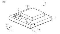
- FIG. 2 is a schematic perspective view of a high-frequency module using the circuit board according to the first embodiment.
- 3A is a cross-sectional view (a Y1-Y1 cross-sectional view in FIG. 2) when a part of the circuit board according to Embodiment 1 is viewed from the front.
- FIG. 3B is a cross-sectional view (a Z1-Z1 cross-sectional view in FIG. 3A) when a part of the circuit board according to Embodiment 1 is viewed from above.
- FIG. 4 is a cross-sectional view of a part of the circuit board according to the modification of the first embodiment when viewed from the front.
- FIG. 1 is a plan view of a part of a circuit board in a comparative example.
- FIG. 2 is a schematic perspective view of a high-frequency module using the circuit board according to the first embodiment.
- 3A is a cross
- FIG. 5 is a cross-sectional view of a part of the circuit board according to the second embodiment as viewed from above.
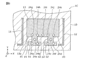
- FIG. 6 is a cross-sectional view of a part of the circuit board according to the first modification of the second embodiment when viewed from above.
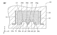
- FIG. 7 is a cross-sectional view of a part of the circuit board according to the second modification of the second embodiment when viewed from above.
- FIG. 2 is a schematic perspective view of the high-frequency module 5 incorporated in a mobile phone or a portable information terminal.
- the circuit board 1 is a component of a part of the high-frequency module 5 and has a signal line for transmitting a high-frequency signal.
- Mounted on the circuit board 1 are various chip components, a high frequency filter, a transmission filter and a reception filter as a diplexer, and mounting electronic components 6 such as a power amplification semiconductor element.
- FIG. 3A is a cross-sectional view (a Y1-Y1 cross-sectional view in FIG. 2) when a part of the circuit board 1 according to the present embodiment is viewed from the front
- FIG. 3B is a cross-sectional view taken along the line (Z1-Z1 cross-sectional view in FIG. 3A).
- 3A and 3B are diagrams showing the end portion of the circuit board 1 extracted.
- FIG. 3A and subsequent drawings for the sake of simplicity, the same type of components are shown in the same pattern, the reference numerals are omitted as appropriate, and strictly speaking, components in different cross sections may be shown and described in the same drawing.
- a circuit board 1 according to the present embodiment is a multilayer structure, and is provided between a board body 10, a plurality of signal lines 11 and 12 for transmitting high-frequency signals, and a plurality of signal lines 11 and 12.
- a ground electrode 13 and a plurality of via conductors 14 (14a to 14g) connected to the ground electrode 13 are provided.
- the ground electrode 13 is connected to the substrate ground 15 via a plurality of via conductors 14, an intermediate ground 16 and an intermediate via 17.
- the substrate body 10 for example, electrical elements such as an inductor, a capacitor, and a resistor, and lead wirings for connecting these electrical elements are formed (not shown).
- the material of the substrate body 10 is, for example, LTCC ceramics (Low Temperature Co-fired Ceramics).
- the plurality of signal lines 11 and 12 are conductor lines provided inside the substrate body 10 in order to electrically connect the electric elements and the mounting electronic component 6 described above.
- the two signal lines 11 and 12 face each other in a predetermined plane (XY plane) and are provided in parallel to the X direction.
- the ground electrode 13 is provided with an interval between the two signal lines 11 and 12.
- the ground electrode 13 is a flat (flat) conductor having a predetermined thickness, and is formed so as to spread in a direction perpendicular to the stacking direction of the circuit board 1 that is a multilayer structure.
- the ground electrode 13 is provided at a position where the distance between the opposing signal lines 11 and 12 is the smallest.
- a part of the outer edge of the ground electrode 13 is formed with a concavo-convex portion 13a protruding outward and recessed inward.
- the outer side or the inner side shown here means, for example, the area of the ground electrode 13 based on the straight line when it is assumed that a straight line is formed along the direction in which the outer edge of the ground electrode 13 extends.
- the direction of decreasing is the inner side, and the direction of increasing the area is the outer side.
- the ground electrode 13 has a substantially rectangular outer shape, and of the outer edges, the outer edges extending along the opposing direction of the signal lines 11 and 12 have a square-wave-like uneven shape. Yes.
- the ground electrode 13 has a convex portion p (p1, p2, p3) protruding to the Y direction minus side and a concave portion d (d1, d2, d3, d4) recessed to the Y direction plus side.
- the convex portions p and the concave portions d are alternately formed at an equal pitch.
- the protrusion dimension of the convex part p is 0.15 mm
- the width of the convex part p is 0.15 mm
- the width of the concave part d is 0.15 mm
- the pitch between the convex part p and the concave part d is 0.15 mm.
- Via conductors 14 are columnar interlayer conductors provided in the substrate body 10. One end of each via conductor 14 is connected to the ground electrode 13. The other end of each via conductor 14 is connected to a substrate ground 15 provided on the bottom side of the substrate body 10 via an intermediate ground 16 provided in the substrate body 10 and an intermediate via 17. .
- the substrate ground 15 is grounded by a wiring (not shown).
- each via conductor 14 when the circuit board 1 is viewed in plan, one end of each via conductor 14 is connected to the uneven portion 13a of the ground electrode 13 corresponding to the uneven shape of the uneven portion 13a.
- one end of each of the via conductors 14a, 14b, and 14c is provided in the convex portion p of the ground electrode 13 and at the center of the corresponding convex portions p1, p2, and p3.
- One end of each of the via conductors 14d, 14e, 14f, and 14g is located on the inner side (Y direction plus side) of the concave portion d of the ground electrode 13 and in the center of the corresponding concave portions d1, d2, d3, and d4 in the X direction.
- the via conductor 14 has a circular shape, and its diameter is smaller than the projecting dimension and width of the convex portion p.
- the diameter of the via conductor 14 is, for example, 0.10 mm.
- the via conductors 14 are also arranged at the same pitch in the X direction and alternately in the Y direction. The position is changed to a zigzag shape.
- a plurality of via holes are formed in each ceramic green sheet, and a conductive paste is filled in these via holes, thereby obtaining a ceramic green sheet having a plurality of via conductor patterns.
- a conductive paste is printed in a predetermined pattern on one ceramic green sheet on which a via conductor pattern is formed to form a ground electrode pattern and a plurality of signal line patterns.
- a ground electrode pattern or a signal line pattern may be formed at the same time.
- a conductive paste is printed in a predetermined pattern on the front and back of another ceramic green sheet on which the via conductor pattern is formed to form a substrate ground pattern, an intermediate via pattern, and an intermediate ground pattern.
- the unfired laminated body block is fired in a lump to produce the circuit board 1 having the signal lines 11 and 12, the ground electrode 13, the via conductor 14, the substrate ground 15, the intermediate ground 16, and the intermediate via 17.
- the signal lines 11, 12, the ground electrode 13, the via conductor 14, the substrate ground 15, the intermediate ground 16, and the intermediate via 17 are made of a material having high conductivity, such as silver, copper, tin, Nickel, gold, or an alloy selected from these materials is used.
- the uneven portion 13a is provided on the outer edge of the ground electrode 13
- the length of the edge (edge) of the ground electrode 13 is increased. Therefore, it generated with the current I 1 of the signal line 11, the current path of the excitation current I 2 of the ground electrode 13 becomes longer.
- the via conductor 14 is provided corresponding to the uneven shape of the uneven portion 13a, the portion of the edge of the ground electrode 13 that is close to the via conductor 14 increases. Therefore, the current is released from the current path of the excitation current I 2 through the via conductor 14, the excitation current I 2 flowing through the ground electrode 13 can be reduced, and the excitation current I 3 generated in the signal line 12 can be reduced.
- the isolation between the signal line 11 and the signal line 12 can be improved.
- the length becomes longer. Therefore, escape current through via conductor 14, it is possible to reduce the excitation current I 2 flowing through the ground electrode 13. As a result, the excitation current I 3 generated in the signal line 12 is reduced, and the isolation between the signal line 11 and the signal line 12 can be improved.
- the excitation current I 2 can be appropriately dispersed and reduced. Further, it is possible to suppress the occurrence of radiation noise due to the excitation current I 2.
- the excitation current tends to concentrate on the outer edge of the ground electrode 13 along the opposing direction of the signal lines 11 and 12, the uneven portion 13 a is provided on the portion along the opposing direction of the signal lines 11 and 12. , it is possible to reduce the excitation current I 2. As a result, the isolation between the signal lines 11 and 12 can be improved.
- FIG. 4 is a cross-sectional view of a part of the circuit board 1A according to the modification of the first embodiment when viewed from the front.
- the ground electrode 13 is connected to the substrate ground 15 via a plurality of via conductors 14, an intermediate ground 16 and an intermediate via 17.
- a mounting electronic component 6 is mounted on the main surface 10a of the substrate body 10, and high-frequency signals are likely to wrap around.
- a circuit board is provided. High-frequency signal wraparound on the electronic component mounting surface of 1A can be suppressed. As a result, the isolation between the signal lines 11 and 12 can be improved.
- FIG. 5 is a cross-sectional view of a part of the circuit board 1B according to the second embodiment as viewed from above.
- a via conductor 14 is also formed on the inside of the convex portion p in the circuit board 1B.
- symbol is described and description is abbreviate
- the circuit board 1B includes a board body 10, a plurality of signal lines 11 and 12, a ground electrode 13, and a plurality of via conductors 14 (14a to 14j).
- the circuit board 1B of the present embodiment has via conductors 14h to 14j in addition to the via conductors 14a to 14g described above.
- the via conductors 14h to 14j are connected to the inner side of the convex portion p of the ground electrode 13.
- the via conductors 14h, 14i, and 14j are located on the inner side (Y-direction plus side) of the convex portions p1, p2, and p3 and on the inner side of the concave portion d, respectively. It is provided between each of 14g.
- the via conductors 14 are provided in a multi-row shape along a part of the outer edge of the ground electrode 13. Specifically, the via conductors 14a to 14j are provided in two rows on one side of the ground electrode 13 extending in the opposing direction of the signal lines 11 and 12.
- FIG. 6 is a cross-sectional view of a part of the circuit board 1C according to the first modification of the second embodiment when viewed from above.
- the circuit board 1 ⁇ / b> C has hook-shaped protruding portions b ⁇ b> 1 and b ⁇ b> 2 on the Y direction minus side of the tips of the projections p ⁇ b> 1 and p ⁇ b> 2 of the ground electrode 13, respectively.
- the circuit board 1C includes a substrate body 10, a plurality of signal lines 11 and 12, a ground electrode 13, and a plurality of via conductors 24 (24a to 24k).
- the protruding portion b1 is connected to the tip of the convex portion p1 of the ground electrode 13, and the protruding portion b2 is connected to the tip of the convex portion p2. Due to these connection structures, an uneven portion 13 a is formed on a part of the outer edge of the ground electrode 13.
- the via conductors 24a and 24b are provided side by side in the protruding portion b1, and the via conductors 24c and 24d are provided side by side in the protruding portion b2.
- the via conductors 24e and 24f are provided in the convex portions p1 and p2, respectively, and the via conductors 24g to 24k are provided inside the concave portions d1 to d3, respectively.
- the isolation between the signal lines 11 and 12 can be improved as in the first embodiment.
- FIG. 7 is a cross-sectional view of a part of the circuit board 1D according to the second modification of the second embodiment as viewed from above.
- the ground electrode 13 of the circuit board 1D has an arcuate cutout.
- the circuit board 1D includes a substrate body 10, a plurality of signal lines 11 and 12, a ground electrode 13, and a plurality of via conductors 34 (34a to 34g).
- the ground electrode 13 has two arc-shaped notches. Due to these notches, a concavo-convex portion 13 a is formed at a part of the outer edge of the ground electrode 13.
- Via conductors 34a, 34b, and 34c are connected to the protrusions p1, p2, and p3 of the ground electrode 13, respectively.
- Two via conductors 34d and 34e are connected to the inside of the recess d1
- two via conductors 34f and 34g are connected to the inside of the recess d2.
- the isolation between the signal lines 11 and 12 can be improved as in the first embodiment.
- the uneven portion of the ground electrode is formed in the opposing direction (X direction) of the two signal lines, and a plurality of via conductors are arranged correspondingly, but the present invention is not limited to this.
- An uneven portion of the ground electrode may be formed in the extending direction (Y direction), and a plurality of via conductors may be arranged correspondingly.
- a plurality of via conductors may be formed in one convex portion.
- the pitch for arranging the plurality of via conductors may be different.
- the two signal lines and the ground electrode are not limited to the end of the circuit board, and may be provided at the center of the circuit board. If the ground electrode is disposed between the two signal lines, the two signal lines and the ground electrode may be provided at different positions in the thickness direction (Z direction) of the circuit board. When three or more signal lines are provided in the circuit board, a ground electrode may be provided between the signal lines facing each other.
- the present invention can be widely used as a circuit board of a high-frequency module built in a wireless communication device or the like.
Landscapes
- Engineering & Computer Science (AREA)
- Microelectronics & Electronic Packaging (AREA)
- Physics & Mathematics (AREA)
- Electromagnetism (AREA)
- Manufacturing & Machinery (AREA)
- Structure Of Printed Boards (AREA)
Abstract
高周波信号を伝送する複数の信号ラインを有する回路基板において、信号ライン間のアイソレーション性を高める。高周波信号を伝送する複数の信号ライン(11、12)と、複数の信号ライン(11、12)の間にて、複数の信号ライン(11、12)のそれぞれに対して間隔をあけて設けられているグランド電極(13)と、グランド電極(13)に接続されている複数のビア導体(14(14a~14g))とを備える回路基板(1)であって、回路基板(1)を平面視した場合に、グランド電極(13)の外縁の少なくとも一部に、外側に突出し内側に窪む凹凸部(13a)が形成されている。複数のビア導体(14(14a~14g))は、凹凸部(13a)の凹凸形状に対応して、凹凸部(13a)に設けられている。
Description
本発明は、回路基板に関し、特に、高周波信号を伝送する信号ラインを有する回路基板に関する。
携帯電話や携帯情報端末には、各種チップ部品、フィルタ、半導体素子などを搭載した高周波モジュールが内蔵されている。そして、この高周波モジュールの一部である回路基板には、高周波信号を伝送する信号ラインが設けられている(例えば、特許文献1)。
特許文献1に記載された回路基板は、信号ラインである送信電極および受信電極を備えている。この送信電極と受信電極との間には、接地電極(グランド電極)が設けられ、そして、この接地電極の端縁と重なるように、複数のビア導体が形成されている。
回路基板の高集積化が進む中で、従来技術に示す回路基板では以下の問題がある。図1は、従来技術の問題点を説明するための、比較例における回路基板101の一部の平面図である。
比較例における回路基板101は、基板本体110と、高周波信号を伝送する2つの信号ライン111、112と、2つの信号ライン111、112の間に設けられているグランド電極113と、グランド電極113に接続されている複数のビア導体114とを備えている。
グランド電極113は、略四角形状の導体であり、向かい合う2つの信号ライン111、112のそれぞれに対して間隔をあけて設けられている。
ビア導体114は、柱状の層間導体である。ビア導体114のそれぞれの一端は、グランド電極113の外縁の一辺に沿ってグランド電極113に接続されている。ビア導体114のそれぞれの他端は、図中の奥行き方向にて接地されている(図示省略)。
このような構造を有する回路基板101では、例えば、一方の信号ライン111に高周波信号による電流I101が流れた場合に、グランド電極113の縁(エッジ)に沿って励起電流I102が流れる。また、この励起電流I102によって、他方の信号ライン112にも励起電流I103が流れる。
そして、比較例における回路基板101では、この励起電流I102の伝搬を抑制するため、グランド電極113に複数のビア導体114を接続することで、励起電流I102の一部を接地側に逃がしている。この構造により、信号ライン111、112間のアイソレーション性を高めている。
しかしながら、回路基板101の高集積化が進む中で、2つの信号ライン111、112間に、より高いアイソレーション性が求められている。それに対し、比較例や従来技術に示す構造の回路基板では、励起電流I102の伝搬を抑制することが不十分であった。そのため、信号ライン111、112間の高いアイソレーション性を実現することが困難であった。
本発明は、高周波信号を伝送する複数の信号ラインを有する回路基板において、信号ライン間のアイソレーション性を高めた回路基板を提供する。
上記目的を達成するために、本発明の一態様に係る回路基板は、高周波信号を伝送する複数の信号ラインと、前記複数の信号ラインの間にて、前記複数の信号ラインのそれぞれに対して間隔をあけて設けられているグランド電極と、前記グランド電極に接続されている複数のビア導体とを備える回路基板であって、前記回路基板を平面視した場合に、前記グランド電極の外縁の少なくとも一部に、外側に突出し内側に窪む凹凸部が形成されており、前記複数のビア導体は、前記凹凸部の凹凸形状に対応して前記凹凸部に設けられている。
このように、グランド電極の外縁に凹凸部が設けられているので、グランド電極の縁(エッジ)の長さが長くなる。そのため、複数の信号ラインのうちの一方の信号ラインの電流に伴って発生する、グランド電極の励起電流の電流経路が長くなる。これにより、グランド電極を流れる励起電流を小さくすることができ、他方の信号ラインに発生する励起電流も小さくできる。また、ビア導体が、凹凸部の凹凸形状に対応して設けられているので、グランド電極の縁の、ビア導体に近接する部分が増える。そのため、励起電流の電流経路からビア導体を通して電流を逃がして、グランド電極に流れる励起電流を減らし、他方の信号ラインに発生する励起電流を減らすことができる。これらの結果、一方の信号ラインと他方の信号ラインとのアイソレーション性を高めることができる。
また、前記複数のビア導体は、平面視で、前記凹凸部の凸部内、および、凹部より内側にそれぞれ設けられていてもよい。
これによれば、グランド電極に流れる励起電流の電流経路のうちの、ビア導体に近接する経路が長くなる。そのため、ビア導体を通して電流を逃がして、グランド電極に流れる励起電流を減らし、他方の信号ラインに発生する励起電流を減らすことができる。その結果、信号ライン間のアイソレーション性を高めることができる。
また、さらに、前記複数のビア導体は、平面視で、前記凸部よりも内側に設けられていてもよい。
これによれば、グランド電極に流れる励起電流の電流経路のうちの、ビア導体に近接する部分が増え、ビア導体に近接する経路がさらに長くなる。そのため、ビア導体を通して電流を逃がして、グランド電極に流れる励起電流を減らし、信号ラインに発生する励起電流を減らすことができる。その結果、信号ライン間のアイソレーション性を高めることができる。
また、前記複数のビア導体は、前記グランド電極の外縁に沿って多列状に設けられていてもよい。
これによれば、グランド電極を流れる励起電流の電流経路のうちの、多列状のビア導体に近接する経路がさらに長くなる。そのため、ビア導体を通して電流を逃がして、グランド電極に流れる励起電流を減らし、信号ラインに発生する励起電流を減らすことができる。その結果、信号ライン間のアイソレーション性を高めることができる。
また、前記グランド電極の前記凹凸部の凸部と凹部とが、交互に等ピッチで形成されていてもよい。
これによれば、励起電流を適切に分散して減らすことができる。
また、前記複数の信号ラインは、所定面内において対向しており、前記グランド電極の前記凹凸部は、前記外縁のうちの、前記複数の信号ラインの対向方向に沿う部分に設けられていてもよい。
グランド電極の外縁のうち、複数の信号ラインの対向方向に沿う部分には励起電流が集中しやすいので、上記構成とすることにより、励起電流を減らし、信号ライン間のアイソレーション性を高めることができる。
また、前記グランド電極および前記複数の信号ラインは、前記回路基板の電子部品実装面に設けられていてもよい。
これによれば、回路基板の電子部品実装面において、高周波信号の回り込みを抑制し、一方の信号ラインを起因とする他方の信号ラインに発生する励起電流を減らすことができる。その結果、信号ライン間のアイソレーション性を高めることができる。
本発明によれば、回路基板に形成された複数の信号ライン間のアイソレーション性を高めることができる。
以下、本発明の実施の形態について、図面を用いて詳細に説明する。なお、以下で説明する実施の形態は、いずれも包括的または具体的な例を示すものである。以下の実施の形態で示される数値、形状、材料、構成要素、構成要素の配置および接続形態、製造工程、および製造工程の順序などは、一例であり、本発明を限定する主旨ではない。以下の実施の形態における構成要素のうち、独立請求項に記載されていない構成要素については、任意の構成要素として説明される。また、図面に示される構成要素の大きさまたは大きさの比は、必ずしも厳密ではない。また、以下の実施の形態において、「接続される」とは、直接接続される場合だけでなく、他の素子等を介して電気的に接続される場合も含まれる。
(実施の形態1)
図2は、携帯電話や携帯情報端末などに内蔵される高周波モジュール5の概略斜視図である。回路基板1は、高周波モジュール5の一部の構成要素であり、高周波信号を伝送する信号ラインを有している。回路基板1には、各種チップ部品、高周波フィルタ、ディプレクサとしての送信用フィルタおよび受信用フィルタ、電力増幅用半導体素子などの実装用電子部品6が搭載される。
図2は、携帯電話や携帯情報端末などに内蔵される高周波モジュール5の概略斜視図である。回路基板1は、高周波モジュール5の一部の構成要素であり、高周波信号を伝送する信号ラインを有している。回路基板1には、各種チップ部品、高周波フィルタ、ディプレクサとしての送信用フィルタおよび受信用フィルタ、電力増幅用半導体素子などの実装用電子部品6が搭載される。
図3Aは、本実施の形態に係る回路基板1の一部を正面から見たときの断面図(図2におけるY1-Y1断面図)であり、図3Bは、回路基板1の一部を上から見たときの断面図(図3AにおけるZ1-Z1断面図)である。なお、図3Aおよび図3Bは、回路基板1の端部を抜き出して示した図である。図3A以下では、簡明のため、同種の構成要素を同じ模様で示して符号を適宜省略し、また、厳密には別断面にある構成要素を同一図面内に示して説明することがある。
本実施の形態に係る回路基板1は、多層構造体であり、基板本体10と、高周波信号を伝送する複数の信号ライン11、12と、複数の信号ライン11、12の間に設けられているグランド電極13と、グランド電極13に接続されている複数のビア導体14(14a~14g)とを備えている。グランド電極13は、複数のビア導体14、中間グランド16および中間ビア17を介して基板グランド15に接続されている。
基板本体10の内部には、例えば、インダクタ、キャパシタ、抵抗などの電気素子や、これらの電気素子を接続する引き回し配線が形成されている(図示省略)。基板本体10の材料は、例えは、LTCCセラミックス(Low Temperature Co-fired Ceramics)である。
複数の信号ライン11、12は、前述した電気素子や実装用電子部品6を電気的に接続するため、基板本体10の内部に設けられている導体線路である。本実施の形態では、一例として、2つの信号ライン11、12が、所定面(XY面)内において対向するとともに、X方向に平行に設けられている。
グランド電極13は、2つの信号ライン11、12に対してそれぞれ間隔をあけて設けられている。グランド電極13は、所定の厚みを有する平面状(平坦形状)の導体であり、多層構造体である回路基板1の積層方向に対して垂直方向に広がるように形成されている。また、グランド電極13は、向かい合う信号ライン11、12の距離が最も小さくなる箇所に設けられる。回路基板1を平面視した場合、グランド電極13の外縁の一部には、外側に突出し内側に窪む凹凸部13aが形成されている。なお、ここで示す外側又は内側とは、例えば、グランド電極13の外縁が延びている方向に沿って直線が形成されていると仮定した場合に、その直線を基準にしてグランド電極13の面積を小さくする方向が内側であり、面積を大きくする方向が外側である。
具体的には、グランド電極13は略矩形状の外形をしており、その外縁のうちの、信号ライン11、12の対向方向に沿って延びている外縁が、方形波状の凹凸形状となっている。すなわち、グランド電極13は、Y方向マイナス側に突出する凸部p(p1、p2、p3)と、Y方向プラス側に窪む凹部d(d1、d2、d3、d4)とを有している。凸部pと凹部dは、交互に等ピッチで形成されている。例えば、凸部pの突出寸法は0.15mm、凸部pの幅は0.15mm、凹部dの幅は0.15mm、凸部pと凹部dとのピッチは、0.15mmである。
ビア導体14(14a~14g)は、基板本体10に設けられている柱状の層間導体である。ビア導体14のそれぞれの一端は、グランド電極13に接続されている。ビア導体14のそれぞれの他端は、基板本体10の内部に設けられた中間グランド16、および、中間ビア17を介して、基板本体10の底面側に設けられた基板グランド15に接続されている。基板グランド15は、図示しない配線により接地される。
本実施の形態では、回路基板1を平面視した場合に、ビア導体14のそれぞれの一端は、凹凸部13aの凹凸形状に対応して、グランド電極13の凹凸部13aに接続されている。具体的には、ビア導体14a、14b、14cの一端は、グランド電極13の凸部p内であって、対応する凸部p1、p2、p3の中央にそれぞれ設けられている。また、ビア導体14d、14e、14f、14gの一端は、グランド電極13の凹部dよりも内側(Y方向プラス側)であって、対応する凹部d1、d2、d3、d4のX方向の中央にそれぞれ設けられている。ビア導体14は円形状であり、その直径は凸部pの突出寸法や幅よりも小さい。ビア導体14の直径は、例えば、0.10mmである。
なお、本実施の形態では、グランド電極13の凸部pと凹部dとが、交互に等ピッチで形成されているので、ビア導体14も、X方向に等ピッチで、かつ、Y方向に交互に位置を替えて千鳥状に形成されている。
次に、回路基板1の製造方法について説明する。
まず、複数のセラミックグリーンシートを準備した後、それぞれのセラミックグリーンシートに複数のビア孔を形成し、これらのビア孔に導電ペーストを充填することで、複数のビア導体パターンを有するセラミックグリーンシートを形成する。
次に、ビア導体パターンが形成された1つのセラミックグリーンシートに、導電ペーストを所定パターンで印刷して、グランド電極パターンおよび複数の信号ラインパターンを形成する。なお、ビア孔に導電ペーストを充填する際に、同時に、グランド電極パターンや信号ラインパターンを形成してもよい。
一方、ビア導体パターンが形成された他のセラミックグリーンシートの表裏に、導電ペーストを所定パターンで印刷して、基板グランドパターン、中間ビアパターンおよび中間グランドパターンを形成する。
次に、これら複数種類のセラミックグリーンシートを所定の順序で積み重ねて一体化し、未焼成積層体ブロックを形成する。その後、未焼成積層体ブロックを一括して焼成することで、信号ライン11、12、グランド電極13、ビア導体14、基板グランド15、中間グランド16および中間ビア17を有する回路基板1を作製する。
なお、これら信号ライン11、12、グランド電極13、ビア導体14、基板グランド15、中間グランド16および中間ビア17の材料としては、導電率の高い材料が用いられ、例えば、銀、銅、錫、ニッケル、金、または、これらの材料から選択される合金などが用いられる。
本実施の形態は、前述したように、グランド電極13の外縁に凹凸部13aが設けられているので、グランド電極13の縁(エッジ)の長さが長くなる。そのため、信号ライン11の電流I1に伴って発生する、グランド電極13の励起電流I2の電流経路が長くなる。
また、ビア導体14が、凹凸部13aの凹凸形状に対応して設けられているので、グランド電極13の縁の、ビア導体14に近接する部分が増える。そのため、励起電流I2の電流経路からビア導体14を通して電流を逃がして、グランド電極13に流れる励起電流I2を減らし、信号ライン12に発生する励起電流I3を減らすことができる。
これらの結果、信号ライン11と信号ライン12とのアイソレーション性を高めることができる。
また、複数のビア導体14が、グランド電極13の凸部p内、および、凹部dより内側にそれぞれ接続されているので、励起電流I2の電流経路のうちの、ビア導体14に近接する経路長が長くなる。そのため、ビア導体14を通して電流を逃がし、グランド電極13に流れる励起電流I2を減らすことができる。その結果、信号ライン12に発生する励起電流I3が減り、信号ライン11と信号ライン12とのアイソレーション性を高めることができる。
また、グランド電極13の凸部pと凹部dが、交互に等ピッチで形成されているので、励起電流I2を適切に分散して減らすことができる。また、励起電流I2に起因する放射ノイズ等の発生を抑制することができる。
また、グランド電極13の外縁のうち、信号ライン11、12の対向方向に沿う部分には励起電流が集中しやすいので、信号ライン11、12の対向方向に沿う部分に凹凸部13aを設けることで、励起電流I2を減らすことができる。その結果、信号ライン11、12間のアイソレーション性を高めることができる。
図4は、実施の形態1の変形例における回路基板1Aの一部を正面から見たときの断面図である。この回路基板1Aには、2つの信号ライン11、12、および、グランド電極13が基板本体10の主面10aに形成されている。グランド電極13は、複数のビア導体14、中間グランド16および中間ビア17を介して基板グランド15に接続されている。
基板本体10の主面10aには、実装用電子部品6が搭載され、高周波信号の回り込みが発生しやすくなるが、電子部品実装面(主面10a)にグランド電極13を設けることで、回路基板1Aの電子部品実装面における、高周波信号の回り込みを抑制することができる。その結果、信号ライン11、12間のアイソレーション性を高めることができる。
なお、回路基板1の内部に位置する中間グランド16の外縁には、凹凸部13aを形成しないことが好ましい。中間グランド16の外縁を凹凸形状とせず、中間グランド16を四角形状とすることで、設計変更する際のビア導体の配置制約が少なくなる。
(実施の形態2)
図5は、実施の形態2に係る回路基板1Bの一部を上から見たときの断面図である。回路基板1Bには、ビア導体14が、凸部pの内側にも形成されている。なお、実施の形態1と共通する構成については、同じ符号を記し、説明を省略する。
図5は、実施の形態2に係る回路基板1Bの一部を上から見たときの断面図である。回路基板1Bには、ビア導体14が、凸部pの内側にも形成されている。なお、実施の形態1と共通する構成については、同じ符号を記し、説明を省略する。
この回路基板1Bは、基板本体10と、複数の信号ライン11、12と、グランド電極13と、複数のビア導体14(14a~14j)とを備えている。
本実施の形態の回路基板1Bは、前述したビア導体14a~14gに加え、ビア導体14h~14jを有している。そして、回路基板1Bを平面視した場合に、これらビア導体14h~14jが、グランド電極13の凸部pよりも内側に接続されている。具体的には、ビア導体14h、14i、14jが、凸部p1、p2、p3よりもそれぞれ内側(Y方向プラス側)に、かつ、凹部dの内側に位置するビア導体14d、14e、14f、14gのそれぞれの間に設けられている。
また、ビア導体14が、グランド電極13の外縁の一部に沿って多列状に設けられている。具体的には、信号ライン11、12の対向方向に延びているグランド電極13の一辺において、ビア導体14a~14jが2列となって設けられている。
この構造により、グランド電極13を流れる励起電流I2の電流経路のうち、ビア導体14に近接する経路長がさらに長くなる。そのため、ビア導体14を通して電流を逃がし、グランド電極13に流れる励起電流I2を減らすことができる。その結果、信号ライン12に発生する励起電流I3が減り、信号ライン11、12間のアイソレーション性を高めることができる。
次に、実施の形態2に関する変形例について説明する。
図6は、実施の形態2の変形例1における回路基板1Cの一部を上から見たときの断面図である。回路基板1Cは、グランド電極13の凸部p1、p2の先端のY方向マイナス側に、鍔状の出っ張り部b1、b2をそれぞれ有している。
この回路基板1Cは、基板本体10と、複数の信号ライン11、12と、グランド電極13と、複数のビア導体24(24a~24k)とを備えている。
そして、グランド電極13の凸部p1の先端に出っ張り部b1が接続され、凸部p2の先端に出っ張り部b2が接続されている。これらの接続構造により、グランド電極13の外縁の一部に凹凸部13aが形成されている。
ビア導体24a、24bは、出っ張り部b1内に並んで設けられ、ビア導体24c、24dは、出っ張り部b2内に並んで設けられている。ビア導体24e、24fは、凸部p1、p2内にそれぞれ設けられ、ビア導体24g~24kは、凹部d1~d3の内側にそれぞれ設けられている。
この回路基板1Cにおいても、実施形態1と同様に、信号ライン11、12間のアイソレーション性を高めることができる。
図7は、実施の形態2の変形例2における回路基板1Dの一部を上から見たときの断面図である。回路基板1Dのグランド電極13は、円弧状の切り欠きを有している。
この回路基板1Dは、基板本体10と、複数の信号ライン11、12と、グランド電極13と、複数のビア導体34(34a~34g)とを備えている。
グランド電極13には、円弧状の2つの切り欠きが形成されている。これらの切り欠きにより、グランド電極13の外縁の一部に凹凸部13aが形成されている。そして、グランド電極13の凸部p1、p2、p3内には、ビア導体34a、34b、34cがそれぞれ接続されている。凹部d1の内側には2つのビア導体34d、34eが接続され、凹部d2の内側には2つのビア導体34f、34gが接続されている。
この回路基板1Dにおいても、実施形態1と同様に、信号ライン11、12間のアイソレーション性を高めることができる。
以上、本発明の実施の形態及びその変形例に係る回路基板について説明したが、本発明は、個々の実施の形態及びその変形例には限定されない。本発明の趣旨を逸脱しない限り、当業者が思いつく各種変形を本実施の形態及びその変形例に施したものや、異なる実施の形態及びその変形例における構成要素を組み合わせて構築される形態も、本発明の一つ又は複数の態様の範囲内に含まれてもよい。
例えば、本実施の形態では、2つの信号ラインの対向方向(X方向)にグランド電極の凹凸部を形成し、それに対応して複数のビア導体を配列したが、それに限られず、2つの信号ラインの延びる方向(Y方向)にグランド電極の凹凸部を形成し、それに対応して複数のビア導体を配列してもよい。
また、1つの凸部内に複数のビア導体を形成してもよい。複数のビア導体を配置するピッチは、異なっていてもよい。
また、2つの信号ラインおよびグランド電極は、回路基板の端部に限られず、回路基板の中央に設けられていてもよい。2つの信号ラインの間にグランド電極が配置されていれば、2つの信号ラインおよびグランド電極は、回路基板の厚み方向(Z方向)の異なる位置にそれぞれ設けられていてもよい。回路基板内に3以上の信号ラインが設けられている場合は、互いに向かい合う信号ラインの間にグランド電極を設ければよい。
本発明は、無線通信装置などに内蔵される高周波モジュールの回路基板として広く利用できる。
1、1A、1B、1C、1D 回路基板
5 高周波モジュール
6 実装用電子部品
10 基板本体
10a 基板本体の主面
11、12 信号ライン
13 グランド電極
13a グランド電極の凹凸部
14、14a~14j、24、24a~24k、34、34a~34g ビア導体
15 基板グランド
16 中間グランド
17 中間ビア
p、p1~p4 グランド電極の凸部
d、d1~d5 グランド電極の凹部
5 高周波モジュール
6 実装用電子部品
10 基板本体
10a 基板本体の主面
11、12 信号ライン
13 グランド電極
13a グランド電極の凹凸部
14、14a~14j、24、24a~24k、34、34a~34g ビア導体
15 基板グランド
16 中間グランド
17 中間ビア
p、p1~p4 グランド電極の凸部
d、d1~d5 グランド電極の凹部
Claims (7)
- 高周波信号を伝送する複数の信号ラインと、
前記複数の信号ラインの間にて、前記複数の信号ラインのそれぞれに対して間隔をあけて設けられているグランド電極と、
前記グランド電極に接続されている複数のビア導体と
を備える回路基板であって、
前記回路基板を平面視した場合に、
前記グランド電極の外縁の少なくとも一部に、外側に突出し内側に窪む凹凸部が形成されており、
前記複数のビア導体は、前記凹凸部の凹凸形状に対応して前記凹凸部に設けられている
回路基板。 - 前記複数のビア導体は、平面視で、前記凹凸部の凸部内、および、凹部より内側にそれぞれ設けられている
請求項1に記載の回路基板。 - さらに、
前記複数のビア導体は、平面視で、前記凸部よりも内側に設けられている
請求項2に記載の回路基板。 - 前記複数のビア導体は、前記グランド電極の前記外縁に沿って多列状に設けられている
請求項1~3のいずれか1項に記載の回路基板。 - 前記グランド電極の前記凹凸部の凸部と凹部とが、交互に等ピッチで形成されている
請求項1~4のいずれか1項に記載の回路基板。 - 前記複数の信号ラインは、所定面内において対向しており、
前記グランド電極の前記凹凸部は、前記外縁のうちの、前記複数の信号ラインの対向方向に沿う部分に設けられている
請求項1~5のいずれか1項に記載の回路基板。 - 前記グランド電極および前記複数の信号ラインは、前記回路基板の電子部品実装面に設けられている
請求項1~6のいずれか1項に記載の回路基板。
Priority Applications (1)
| Application Number | Priority Date | Filing Date | Title |
|---|---|---|---|
| US15/966,227 US10524353B2 (en) | 2015-11-04 | 2018-04-30 | Circuit board |
Applications Claiming Priority (2)
| Application Number | Priority Date | Filing Date | Title |
|---|---|---|---|
| JP2015217129 | 2015-11-04 | ||
| JP2015-217129 | 2015-11-04 |
Related Child Applications (1)
| Application Number | Title | Priority Date | Filing Date |
|---|---|---|---|
| US15/966,227 Continuation US10524353B2 (en) | 2015-11-04 | 2018-04-30 | Circuit board |
Publications (1)
| Publication Number | Publication Date |
|---|---|
| WO2017077853A1 true WO2017077853A1 (ja) | 2017-05-11 |
Family
ID=58662693
Family Applications (1)
| Application Number | Title | Priority Date | Filing Date |
|---|---|---|---|
| PCT/JP2016/080811 Ceased WO2017077853A1 (ja) | 2015-11-04 | 2016-10-18 | 回路基板 |
Country Status (2)
| Country | Link |
|---|---|
| US (1) | US10524353B2 (ja) |
| WO (1) | WO2017077853A1 (ja) |
Citations (3)
| Publication number | Priority date | Publication date | Assignee | Title |
|---|---|---|---|---|
| JPH11330298A (ja) * | 1998-05-12 | 1999-11-30 | Murata Mfg Co Ltd | 信号端子付パッケージおよびそれを用いた電子装置 |
| WO2011136100A1 (ja) * | 2010-04-30 | 2011-11-03 | 株式会社村田製作所 | 複合部品 |
| WO2012176401A1 (ja) * | 2011-06-21 | 2012-12-27 | 株式会社村田製作所 | 回路モジュール |
Family Cites Families (2)
| Publication number | Priority date | Publication date | Assignee | Title |
|---|---|---|---|---|
| JPH10135704A (ja) | 1996-10-29 | 1998-05-22 | Hitachi Metals Ltd | ダイオードスイッチ |
| JP2005217581A (ja) | 2004-01-28 | 2005-08-11 | Kyocera Corp | 高周波電力増幅モジュール、高周波モジュール及び無線通信装置 |
-
2016
- 2016-10-18 WO PCT/JP2016/080811 patent/WO2017077853A1/ja not_active Ceased
-
2018
- 2018-04-30 US US15/966,227 patent/US10524353B2/en active Active
Patent Citations (3)
| Publication number | Priority date | Publication date | Assignee | Title |
|---|---|---|---|---|
| JPH11330298A (ja) * | 1998-05-12 | 1999-11-30 | Murata Mfg Co Ltd | 信号端子付パッケージおよびそれを用いた電子装置 |
| WO2011136100A1 (ja) * | 2010-04-30 | 2011-11-03 | 株式会社村田製作所 | 複合部品 |
| WO2012176401A1 (ja) * | 2011-06-21 | 2012-12-27 | 株式会社村田製作所 | 回路モジュール |
Also Published As
| Publication number | Publication date |
|---|---|
| US10524353B2 (en) | 2019-12-31 |
| US20180249575A1 (en) | 2018-08-30 |
Similar Documents
| Publication | Publication Date | Title |
|---|---|---|
| US8994470B2 (en) | Circuit substrate having noise suppression structure | |
| CN207603991U (zh) | 柔性电路板 | |
| JP5737457B2 (ja) | 信号線路モジュールおよび通信端末装置 | |
| US9844138B2 (en) | Multilayer wiring board | |
| US10916938B2 (en) | ESD-protective surface-mount composite component | |
| US20170257941A1 (en) | Radio frequency module | |
| US9099764B2 (en) | Electronic circuit and electronic device | |
| CN104054141B (zh) | 扁平电缆及电子设备 | |
| JP6406474B2 (ja) | 表面実装型シールド部材及び回路モジュール | |
| JP5704177B2 (ja) | 電子部品 | |
| JP6949640B2 (ja) | アレイアンテナ基板 | |
| JP6224484B2 (ja) | 方向性結合器および高周波モジュール | |
| WO2019044425A1 (ja) | 多層基板及びアンテナモジュール | |
| JP6510350B2 (ja) | 方向性結合器および高周波モジュール | |
| WO2017077853A1 (ja) | 回路基板 | |
| US20090008134A1 (en) | Module | |
| CN110556622B (zh) | 天线装置、天线基板及天线元件 | |
| JP3830046B2 (ja) | 方向性結合器 | |
| KR100558443B1 (ko) | 저온 소성 세라믹 기판의 외부 단자 구조 및 그 형성방법 | |
| JP7282570B2 (ja) | アンテナ及び半導体装置 | |
| JP2007288418A (ja) | アンテナ装置 | |
| JP2016219615A (ja) | プリント配線基板 |
Legal Events
| Date | Code | Title | Description |
|---|---|---|---|
| 121 | Ep: the epo has been informed by wipo that ep was designated in this application |
Ref document number: 16861919 Country of ref document: EP Kind code of ref document: A1 |
|
| NENP | Non-entry into the national phase |
Ref country code: DE |
|
| 122 | Ep: pct application non-entry in european phase |
Ref document number: 16861919 Country of ref document: EP Kind code of ref document: A1 |
|
| NENP | Non-entry into the national phase |
Ref country code: JP |