WO2017077841A1 - 中継装置、電子制御装置及び車載ネットワークシステム - Google Patents
中継装置、電子制御装置及び車載ネットワークシステム Download PDFInfo
- Publication number
- WO2017077841A1 WO2017077841A1 PCT/JP2016/080635 JP2016080635W WO2017077841A1 WO 2017077841 A1 WO2017077841 A1 WO 2017077841A1 JP 2016080635 W JP2016080635 W JP 2016080635W WO 2017077841 A1 WO2017077841 A1 WO 2017077841A1
- Authority
- WO
- WIPO (PCT)
- Prior art keywords
- bus
- signal
- relay device
- buses
- period
- Prior art date
- Legal status (The legal status is an assumption and is not a legal conclusion. Google has not performed a legal analysis and makes no representation as to the accuracy of the status listed.)
- Ceased
Links
Images


Classifications
-
- H—ELECTRICITY
- H04—ELECTRIC COMMUNICATION TECHNIQUE
- H04L—TRANSMISSION OF DIGITAL INFORMATION, e.g. TELEGRAPHIC COMMUNICATION
- H04L12/00—Data switching networks
- H04L12/28—Data switching networks characterised by path configuration, e.g. LAN [Local Area Networks] or WAN [Wide Area Networks]
- H04L12/46—Interconnection of networks
- H04L12/4604—LAN interconnection over a backbone network, e.g. Internet, Frame Relay
- H04L12/4608—LAN interconnection over ATM networks
-
- H—ELECTRICITY
- H04—ELECTRIC COMMUNICATION TECHNIQUE
- H04L—TRANSMISSION OF DIGITAL INFORMATION, e.g. TELEGRAPHIC COMMUNICATION
- H04L12/00—Data switching networks
- H04L12/28—Data switching networks characterised by path configuration, e.g. LAN [Local Area Networks] or WAN [Wide Area Networks]
- H04L12/40—Bus networks
- H04L12/40006—Architecture of a communication node
-
- H—ELECTRICITY
- H04—ELECTRIC COMMUNICATION TECHNIQUE
- H04L—TRANSMISSION OF DIGITAL INFORMATION, e.g. TELEGRAPHIC COMMUNICATION
- H04L12/00—Data switching networks
- H04L12/28—Data switching networks characterised by path configuration, e.g. LAN [Local Area Networks] or WAN [Wide Area Networks]
- H04L12/40—Bus networks
- H04L12/40169—Flexible bus arrangements
- H04L12/40176—Flexible bus arrangements involving redundancy
-
- H—ELECTRICITY
- H04—ELECTRIC COMMUNICATION TECHNIQUE
- H04L—TRANSMISSION OF DIGITAL INFORMATION, e.g. TELEGRAPHIC COMMUNICATION
- H04L12/00—Data switching networks
- H04L12/28—Data switching networks characterised by path configuration, e.g. LAN [Local Area Networks] or WAN [Wide Area Networks]
- H04L12/40—Bus networks
- H04L2012/40208—Bus networks characterized by the use of a particular bus standard
- H04L2012/40215—Controller Area Network CAN
-
- H—ELECTRICITY
- H04—ELECTRIC COMMUNICATION TECHNIQUE
- H04L—TRANSMISSION OF DIGITAL INFORMATION, e.g. TELEGRAPHIC COMMUNICATION
- H04L12/00—Data switching networks
- H04L12/28—Data switching networks characterised by path configuration, e.g. LAN [Local Area Networks] or WAN [Wide Area Networks]
- H04L12/40—Bus networks
- H04L2012/40267—Bus for use in transportation systems
- H04L2012/40273—Bus for use in transportation systems the transportation system being a vehicle
Definitions
- the present invention relates to a relay device, an electronic control device, and an in-vehicle network system.
- CAN FD CAN with Flexible Data rate
- nodes that transmit and receive are generally electronic control units (ECUs), and each node is electrically connected by a bus.
- the transmission ECU composes a message by adding an identifier (ID) to communication data, converts it into an electrical signal, and transmits it on the bus.
- ID identifier
- Each ECU monitors an electrical signal on the bus, acquires an ID during communication, and specifies a message to be received.
- the communication priority is determined according to the ID.
- the phase in which the ECU that can send the ID and can send the message according to the priority order is called an arbitration phase.
- the arbitration phase multiple ECUs output simultaneously, so communication is performed at the same speed as conventional CAN, for example, 500 kbps.
- the data phase for transmitting data is entered. In the data phase in which one output ECU is specified, the transmission speed is 2 Mbps, for example.
- An object of the present invention is to provide a relay device or the like that can suppress reflection of a bus signal and suppress signal delay.
- the present invention provides a relay device that relays a plurality of buses to which a plurality of in-vehicle processing devices are connected, and processes a signal received from one of the plurality of buses.
- the first embodiment includes a relay circuit 100A to which two pairs of buses (CAN1, CAN2) shown in FIG. 1A are connected.
- One pair of buses CAN1 is composed of two buses (CANH1, CANL1), and the other pair of buses CAN2 is composed of two buses (CANH2, CANL2).
- the bus CANH1 is connected to the bus CANH2 via the connection circuit 102 and the buffer circuit 104.
- the bus CANL1 is connected to the bus CANL2 via the connection circuit 103 and the buffer circuit 105.
- the connection circuits (102, 103) are switches that directly and electrically connect the buses.
- the relay circuit 100A relays the bus CAN1 and the bus CAN2, but it goes without saying that a plurality of buses to which a plurality of in-vehicle processing devices are connected may be relayed.
- the plurality of buses include at least a bus CAN1 (first bus) and a bus CAN2 (second bus).
- the relay device 100A includes a signal processing transfer path P1 and a bypass connection path P2, as shown in FIG. 1A.
- the signal processing transfer path P1 processes a signal received from one bus CAN1 of the plurality of buses and transfers it to the other bus CAN2.
- the bypass connection path P2 connects one bus CAN1 and another bus CAN2 by bypassing the signal processing transfer path P1.
- the bypass connection path P2 includes connection circuits 102 and 103 (switches) having one end connected to the bus CAN1 (first bus) and the other end connected to the bus CAN2 (second bus).
- Buffer circuit 104 receives the value of bus CANH1 and outputs the same value to bus CANH2, or receives the value of bus CANH2 and outputs the same value to bus CANH1.
- the buffer circuit 105 receives the value of the bus CANL1 and outputs the same value to the bus CANL2, or receives the value of the bus CANL2 and outputs the same value to the bus CANL1. That is, the logical value of the signal input to the buffer circuit (104, 105) and the logical value of the signal output from the buffer circuit (104, 105) are the same.
- the signal processing transfer path P1 sends an output signal generated based on the first signal received from the bus CAN1 (first bus) to the bus CAN2 (second bus).
- Including buffer circuits 104 and 105 first communication device.
- the signal processing transfer path P1 is a buffer circuit 104 (105) that transmits an output signal generated based on the second signal received from the bus CAN2 (second bus) to the bus CAN1 (first bus).
- Second communication device In the present embodiment, the first communication device and the second communication device are configured integrally, but may be separate.
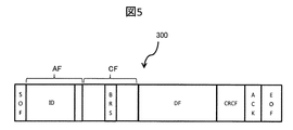
- the first signal and the second signal include the frame 300 shown in FIG.
- the frame 300 includes, for example, SOF (Start Of Frame), arbitration field (AF), control field (CF), CRC field (CRCF), ACK, and EOF (End Of Frame).
- SOF Start Of Frame
- AF arbitration field
- CF control field
- CRC field CRC field
- ACK ACK
- EOF End Of Frame
- Arbitration field AF includes an ID
- control field CF includes a BRS bit.
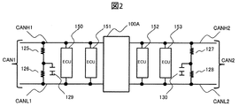
- FIG. 2 shows the network configuration to which this relay circuit is applied.
- the vehicle-mounted electronic control unit ECU (150, 151) is connected to the bus CAN1
- the vehicle-mounted ECU (152, 153) is connected to the other pair of bus CAN2.
- the ECU (150, 151, 152, 153) corresponds to CAN FD.
- CAN FD as a network protocol is an extended CAN communication protocol that can transmit a large amount of data by accelerating the bit rate of only the data phase with respect to the arbitration phase.
- CAN FD transmits data in a mode called recessive and dominant.
- recessive the bus pair is set to the same potential by the termination circuit, and in dominant, 0 or 1 is sent by causing a potential difference in the paired bus by the transceiver.
- an ID identifier is added to the data, and a CRC value is added to the end of the data to ensure communication reliability, and a message is formed, and the data to be transmitted is determined according to priority in the arbitration phase according to the numerical value of the ID. .
- the ID that is the priority of each message, the sending ECU and the receiving ECU are determined at the time of designing the in-vehicle network, and are installed in each ECU.
- Each ECU monitors an electrical signal on the bus, acquires an ID during communication, and specifies a message to be received.
- Resistors (125, 126) are connected as termination resistors to the bus CAN1, and a capacitor 129 is connected to a connection portion between the resistors 125 and 126.
- resistors (127, 128) are connected as termination resistors to the bus CAN2, and a capacitor 130 is connected to a connection portion between the resistors 127 and 128.
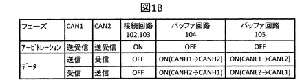
- Figure 1B shows the operation logic.
- the connection circuits (102, 103) are turned on, and the buffer circuits (104, 105) are turned off.
- the ECU connected to the bus CAN1 and the ECU connected to the bus CAN2 can transmit IDs.
- the buffer circuit 104 is turned on and sends the data received from the bus CANH1 to the bus CANH2.
- the buffer circuit 105 is also turned on, and the data received from the bus CANL1 is sent to the bus CANL2.
- the buffer circuit 104 is turned on and sends the data received from the bus CANH2 to the bus CANH1.
- the buffer circuit 105 is also turned on, and the data received from the bus CANL2 is sent to the bus CANL1.
- control circuit 110 has a communication speed of the first signal received from the bus CAN1 (first bus) or the second signal received from the bus CAN2 (second bus) as the first.
- arbitration phase which is a communication speed (for example, 500 kbps)
- the connection circuits 102 and 103 are turned on, and the communication speed of the first or second signal is higher than the first communication speed.
- the connection circuits 102 and 103 are turned off in a data phase (second period) at a communication speed of 2 (for example, 2 Mbps).
- the arbitration phase (first period) is included in the first signal and the second signal, and is connected to the bus CAN1 (first bus) and the bus CAN2 (second bus). At least a period during which an arbitration field for determining a vehicle-mounted control device that transmits data from a plurality of vehicle-mounted control devices is received. This ensures that the bus CAN1 and the bus CAN2 are directly electrically connected in the arbitration phase.
- the control circuit 110 (controller) turns off the buffer circuits 104 and 105 (first and second communication devices) in the arbitration phase (first period), and the buffer circuit 104 in the data phase (second period). , 105 is turned on.
- the arbitration phase signal transfer processing is not performed in the buffer circuits 104 and 105, and signal transfer processing is performed in the data phase.
- the data phase includes at least a period during which the data field included in the first signal and the second signal is received.
- the arbitration phase four ECUs are connected to a pair of buses, and the priority order of the four ECUs is determined.
- the bus size is large, communication is possible because it operates at 500 Mbps.
- the bus is divided and the scale is reduced, so that reflection is reduced in each bus and communication at 2 Mbps is possible.
- the control circuit includes a processor such as a CPU (Central Processing Unit) and a storage device such as a memory.
- a processor such as a CPU (Central Processing Unit)
- a storage device such as a memory.
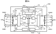
- the second embodiment includes a relay circuit 100B to which two pairs of buses (CAN1, CAN2) shown in FIG. 3A are connected.
- One pair of buses CAN1 is composed of two buses (CANH1, CANL1), and the other pair of buses CAN2 is composed of two buses (CANH2, CANL2).
- a connection circuit 102 and a driver circuit 106 are connected to the bus CANH1.
- a connection circuit 103 and a driver circuit 106 such as a transceiver are connected to the bus CANL1.
- a connection circuit 102 and a driver circuit 107 such as a transceiver are connected to the bus CANH2.
- a connection circuit 103 and a driver circuit 107 are connected to the bus CANL2.
- Resistors (121, 122) are connected as termination resistors to the buses (CANH1, CANL1), and the switch circuit 131 is connected to a connection portion between the resistors 121 and 122.
- Resistors (123, 124) are connected as termination resistors to the buses (CANH2, CANL2), and a switch circuit 132 is connected to a connection portion between the resistors 123 and 124.
- the control circuit 110 receives data signals (RxD1, RxD2) and outputs control signals (SCS1, SCS2, DCS1, DCS2).
- the data signal RxD1 is an output signal of the driver circuit 106
- the data signal RxD2 is an output signal of the driver circuit 107.
- the control signal SCS1 is a signal for controlling the connection circuit 102
- the control signal SCS2 is a signal for controlling the connection circuit 103.
- the logic circuit 115 calculates the logical product of the control signal DCS1 and the data signal RxD2, and outputs the data signal TxD1 to the driver circuit 106.
- the logic circuit 116 calculates the logical product of the control signal DCS2 and the data signal RxD1, and outputs the data signal TxD2 to the driver circuit 107.
- the signal processing transfer path P1 outputs an output signal generated based on the first signal received from the bus CAN1 (first bus) to the bus CAN2 (second bus).
- the signal processing transfer path P1 is a second communication device that transmits an output signal generated based on the second signal received from the bus CAN2 (second bus) to the bus CAN1 (first bus). Including.
- the first communication device includes a driver circuit 106, a logic circuit 116, and a driver circuit 107.
- the second communication device includes a driver circuit 107, a logic circuit 115, and a driver circuit 106.
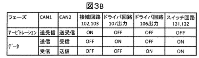
- Fig. 3B shows the operation logic of Fig. 3A.
- the connection circuits (102, 103) are turned on, and the driver circuits (106, 107) are turned off.
- An ECU is connected to each of the bus pair CAN1 and the bus pair CAN2, and an ID can be transmitted.
- the driver circuit 107 is turned on, and the data received from the bus pair CAN1 is sent to the bus pair CAN2.
- the driver circuit 106 is turned on, and the data received from the bus CAN2 is sent to the bus CAN1.
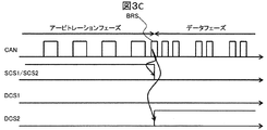
- Fig. 3C shows the operation waveform.
- the BRS Bit rate switch
- the control signals (SCS1, SCS2) are changed from the high level to the low level.
- the connection circuits (102, 103) are turned off.
- the control signal DCS1 or DSC2 changes from the low level to the high level, and the driver circuit 106 or 107 is turned on.
- the beginning of the data phase (second period) is the timing at which a BRS bit included in the first signal and the second signal and indicating an increase in communication speed is received.
- the resistor 121, the switch circuit 131, and the resistor 122 connected in series constitute a first terminal resistor device
- the resistor 123, the switch circuit 132, and the resistor 124 connected in series are a second terminal resistor device.
- the control circuit 110 (controller) turns off the first and second termination resistance devices in the arbitration phase (first period) and the first and second termination resistance devices in the data phase (second period). Turn on.
- the bus pair CAN1 and CAN2 are connected in the arbitration phase, and the priority order is determined by all ECUs connected to each bus pair.
- the bus size is large, communication is possible because it operates at 500 Mbps.
- the bus is divided and the scale is reduced, so that reflection is reduced in each bus and communication at 2 Mbps is possible.
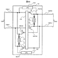
- the third embodiment includes a relay circuit 100C to which two pairs of buses (CAN1 and CAN2) shown in FIG. 4A are connected.
- One pair of buses CAN1 is composed of two buses (CANH1, CANL1), and the other pair of buses CAN2 is composed of two buses (CANH2, CANL2).
- a connection circuit 102 and a control circuit 110 are connected to the bus CANH1.
- a connection circuit 103 and a control circuit 110 are connected to the bus CANL1.
- a connection circuit 102 and a control circuit 110 are connected to the bus CANH2.
- a connection circuit 103 and a control circuit 110 are connected to the bus CANL2.
- Resistors (121, 122) are connected as termination resistors to the buses (CANH1, CANL1), and the switch circuit 131 is connected to a connection portion between the resistors 121 and 122.
- Resistors (123, 124) are connected as termination resistors to the buses (CANH2, CANL2), and a switch circuit 132 is connected to a connection portion between the resistors 123 and 124.
- the control circuit 110 receives the data on the bus CANH1 and drives the transistor PMOS2. It also receives data on the bus CANL1 and drives the transistor NMOS2. Further, it receives data on the bus CANH2 and drives the transistor PMOS1. It also receives data on the bus CANL2 and drives the transistor NMOS1.
- FIG. 4B shows the operation logic of FIG. 4A. In the arbitration phase, the connection circuits (102, 103) are turned on, and the transistors (PMOS1, NMOS1, PMOS2, NMOS2) are turned off. An ECU is connected to each of the bus pair CAN1 and the bus pair CAN2, and an ID can be transmitted.
- the ECU that is determined to transmit data according to the priority in the arbitration phase When the ECU that is determined to transmit data according to the priority in the arbitration phase is connected to the bus pair CAN1, it is turned on depending on the data transmitted through the transistors PMOS2 and NMOS2.
- the switch circuit 132 is also turned on to activate the termination function.
- the ECU that is determined to transmit data according to the priority in the arbitration phase is connected to the bus pair CAN2, the ECU is turned on depending on the data transmitted through the transistors PMOS1 and NMOS1.
- the switch circuit 131 is also turned on to activate the termination function.
- the bus pair CAN1 and CAN2 are connected in the arbitration phase, and the priority order is determined by all ECUs connected to each bus pair.
- the bus size is large, communication is possible because it operates at 500 Mbps.
- the bus is divided and the scale is reduced, so that reflection is reduced in each bus and communication at 2 Mbps is possible.
- the present invention is not limited to the above-described embodiment, and includes various modifications.
- the above-described embodiment has been described in detail for easy understanding of the present invention, and is not necessarily limited to one having all the configurations described.
- a part of the configuration of an embodiment can be replaced with the configuration of another embodiment, and the configuration of another embodiment can be added to the configuration of an embodiment.
- the relay device may be a dedicated device, or the ECU as the gateway ECU may include the same configuration as the relay device.
- each of the above-described configurations, functions, and the like may be realized by hardware by designing a part or all of them with, for example, an integrated circuit.
- Information such as programs, tables, and files for realizing each function can be stored in a recording medium such as a memory.
- the present embodiment may be the following modes.
- a signal processing transfer that relays a plurality of buses to which a plurality of in-vehicle processing devices are connected, and processes a signal received from one of the plurality of buses and transfers the signal to another bus
- a relay apparatus comprising: a path; and a bypass connection path that connects the one bus and the other bus by bypassing the signal processing transfer path.
- the in-vehicle processing device is configured to transmit data after performing arbitration, and when the in-vehicle processing device transmits an arbitration signal, each of the buses A relay device that connects each other via the bypass connection path and connects the buses via the signal processing transfer path when the in-vehicle processing device transmits data.
- An in-vehicle network system including a plurality of buses to which a plurality of in-vehicle processing devices are connected, wherein the plurality of buses are connected by a relay circuit, wherein the in-vehicle processing device transmits data after performing arbitration.
- the data transmission speed is set to be higher than the transmission speed of the signal transmitted during the arbitration, and the relay directly connects one signal of each bus to another bus.
- An in-vehicle network system comprising: a first path; and a second path for transmitting a signal received from one of the buses to another bus.
- the relay circuit when the in-vehicle processing device transmits an arbitration signal, the relay circuit connects the plurality of buses through the first path, and the in-vehicle processing device transmits data. When transmitting the relay, the relay circuit connects the plurality of buses by the second route.
Landscapes
- Engineering & Computer Science (AREA)
- Computer Networks & Wireless Communication (AREA)
- Signal Processing (AREA)
- Small-Scale Networks (AREA)
Abstract
Description
第1の実施の形態は、図1Aに示した2対のバス(CAN1、CAN2)が接続された中継回路100Aで構成される。1対のバスCAN1は2本のバス(CANH1、CANL1)で構成され、もう1対のバスCAN2は2本のバス(CANH2、CANL2)で構成される。バスCANH1は接続回路102とバッファ回路104を介してバスCANH2に接続される。バスCANL1は接続回路103とバッファ回路105を介してバスCANL2に接続される。接続回路(102、103)はバスを電気的に直接導通接続するスイッチである。
を含む。
第2の実施の形態は、図3Aに示した2対のバス(CAN1、CAN2)が接続された中継回路100Bで構成される。1対のバスCAN1は2本のバス(CANH1、CANL1)で構成され、もう1対のバスCAN2は2本のバス(CANH2、CANL2)で構成される。バスCANH1には接続回路102とドライバ回路106が接続される。バスCANL1には接続回路103とトランシーバ等のドライバ回路106が接続される。バスCANH2には接続回路102とトランシーバ等のドライバ回路107が接続される。バスCANL2には接続回路103とドライバ回路107が接続される。バス(CANH1、CANL1)には終端抵抗として抵抗(121、122)が接続されており、スイッチ回路131が抵抗121と抵抗122の接続部分に接続される。バス(CANH2、CANL2)には終端抵抗として抵抗(123、124)が接続されており、スイッチ回路132が抵抗123と抵抗124の接続部分に接続される。
第3の実施の形態は、図4Aに示した2対のバス(CAN1、CAN2)が接続された中継回路100Cで構成される。1対のバスCAN1は2本のバス(CANH1、CANL1)で構成され、もう1対のバスCAN2は2本のバス(CANH2、CANL2)で構成される。バスCANH1には接続回路102と制御回路110が接続される。バスCANL1には接続回路103と制御回路110が接続される。バスCANH2には接続回路102と制御回路110が接続される。バスCANL2には接続回路103と制御回路110が接続される。バス(CANH1、CANL1)には終端抵抗として抵抗(121、122)が接続されており、スイッチ回路131が抵抗121と抵抗122の接続部分に接続される。バス(CANH2、CANL2)には終端抵抗として抵抗(123、124)が接続されており、スイッチ回路132が抵抗123と抵抗124の接続部分に接続される。
102、103…接続回路
104、105…バッファ回路
110…制御回路
121、122、123、124、125、126、127、128…抵抗
131、132…スイッチ回路
129、130…コンデンサ(容量)
150、151、152、153…ECU
106、107…ドライバ回路
115、116…論理回路
201…CAN受信開始
202…CAN ID認識
203…周波数切替有?(BRS=1?)
204…バッファ:ON、スイッチ:OFF
205…データ送信
206…バッファ:OFF、スイッチ:ON
207…ACK受信
208…終了
209…データ送信
Claims (11)
- 複数の車載処理装置が接続される複数のバスを中継する中継装置であって、
前記複数のバスのうちの一つのバスから受信した信号を処理して他のバスに転送する信号処理転送経路と、
前記一つのバスと前記他のバスとを前記信号処理転送経路をバイパスして接続するバイパス接続経路と、
を有することを特徴とする中継装置。 - 請求項1に記載の中継装置であって、
前記複数のバスは、
少なくとも第1のバスと第2のバスを含み、
前記信号処理転送経路は、
前記第1のバスから受信した第1の信号に基づいて生成される出力信号を前記第2のバスへ送信する第1の通信装置と、
前記第2のバスから受信した第2の信号に基づいて生成される出力信号を前記第1のバスへ送信する第2の通信装置と、を含み、
前記バイパス接続経路は、
一端が第1のバスに接続され、他端が第2のバスに接続されるスイッチを含む
ことを特徴とする中継装置。 - 請求項2に記載の中継装置であって、
前記第1又は第2の信号の通信速度が第1の通信速度である第1の期間に、前記スイッチをオンし、前記第1又は第2の信号の通信速度が前記第1の通信速度より大きい第2の通信速度である第2の期間に、前記スイッチをオフするコントローラをさらに備える
ことを特徴とする中継装置。 - 請求項3に記載の中継装置であって、
前記第1の期間は、
前記第1の信号及び前記第2の信号に含まれ、前記第1及び第2のバスに接続される前記複数の車載制御装置からデータを送信する車載制御装置を決めるアービトレーションフィールドが受信される期間を少なくとも含む
ことを特徴とする中継装置。 - 請求項3に記載の中継装置であって、
前記コントローラは、
前記第1の期間に、前記第1及び第2の通信装置をオフし、
前記第2の期間に、前記第1及び第2の通信装置をオンする
ことを特徴とする中継装置。 - 請求項3に記載の中継装置であって、
前記第2の期間は、
前記第1の信号及び前記第2の信号に含まれるデータフィールドが受信される期間を少なくとも含む
ことを特徴とする中継装置。 - 請求項3に記載の中継装置であって、
前記第2の期間の始期は、
前記第1の信号及び前記第2の信号に含まれ、通信速度を大きくすることを示すビットが受信されるタイミングである
ことを特徴とする中継装置。 - 請求項3に記載の中継装置であって、
前記第1のバスに接続される第1の終端抵抗装置と、
前記第2のバスに接続される第2の終端抵抗装置と、をさらに備え、
前記コントローラは、
前記第1の期間に、前記第1及び第2の終端抵抗装置をオフし、
前記第2の期間に、前記第1及び第2の終端抵抗装置をオンする
ことを特徴とする中継装置。 - 請求項1に記載の中継装置を含むことを特徴とする電子制御装置。
- 請求項2に記載の中継装置であって、
前記第1の通信装置と前記第2の通信装置は、
一体に構成される
ことを特徴とする中継装置。 - 複数の車載制御装置と、
前記複数の車載処理装置が接続される複数のバスを中継する中継装置と、を備えた車載ネットワークシステムであって、
前記中継装置は、
前記複数のバスのうちの一つのバスから受信した信号を処理して他のバスに転送する信号処理転送経路と、
前記一つのバスと前記他のバスとを前記信号処理転送経路をバイパスして接続するバイパス接続経路と、を有する
ことを特徴とする車載ネットワークシステム。
Priority Applications (4)
| Application Number | Priority Date | Filing Date | Title |
|---|---|---|---|
| CN201680060324.1A CN108353016B (zh) | 2015-11-05 | 2016-10-17 | 中继装置、电子控制装置以及车载网络系统 |
| DE112016005087.9T DE112016005087B4 (de) | 2015-11-05 | 2016-10-17 | Relaisvorrichtung, elektronische Steuervorrichtung und fahrzeugmontiertes Netzsystem |
| JP2017548695A JP6496836B2 (ja) | 2015-11-05 | 2016-10-17 | 中継装置、電子制御装置及び車載ネットワークシステム |
| US15/768,733 US10484202B2 (en) | 2015-11-05 | 2016-10-17 | Relay device, electronic control device, and vehicle-mounted network system |
Applications Claiming Priority (2)
| Application Number | Priority Date | Filing Date | Title |
|---|---|---|---|
| JP2015-217200 | 2015-11-05 | ||
| JP2015217200 | 2015-11-05 |
Publications (1)
| Publication Number | Publication Date |
|---|---|
| WO2017077841A1 true WO2017077841A1 (ja) | 2017-05-11 |
Family
ID=58661840
Family Applications (1)
| Application Number | Title | Priority Date | Filing Date |
|---|---|---|---|
| PCT/JP2016/080635 Ceased WO2017077841A1 (ja) | 2015-11-05 | 2016-10-17 | 中継装置、電子制御装置及び車載ネットワークシステム |
Country Status (5)
| Country | Link |
|---|---|
| US (1) | US10484202B2 (ja) |
| JP (1) | JP6496836B2 (ja) |
| CN (1) | CN108353016B (ja) |
| DE (1) | DE112016005087B4 (ja) |
| WO (1) | WO2017077841A1 (ja) |
Cited By (3)
| Publication number | Priority date | Publication date | Assignee | Title |
|---|---|---|---|---|
| JP2018207343A (ja) * | 2017-06-06 | 2018-12-27 | 株式会社オートネットワーク技術研究所 | 中継装置、中継方法及び中継プログラム |
| CN111510217A (zh) * | 2020-04-15 | 2020-08-07 | 南京大学 | 一种应用于高速列车的长距离通信的光电混合总线系统 |
| JP2021527372A (ja) * | 2018-09-10 | 2021-10-11 | イノヴァ セミコンダクトルズ ゲーエムベーハー | データフロー制御のためのラインドライバデバイス |
Families Citing this family (3)
| Publication number | Priority date | Publication date | Assignee | Title |
|---|---|---|---|---|
| JP7059899B2 (ja) * | 2018-11-09 | 2022-04-26 | トヨタ自動車株式会社 | ネットワークシステム |
| DE102018220069A1 (de) * | 2018-11-22 | 2020-05-28 | Robert Bosch Gmbh | Reflexionsdämpfungsvorrichtung für einen Bus eines Bussystems und Verfahren zum Dämpfen von Reflexionen bei einer Datenübertragung in einem Bussystem |
| KR20250005730A (ko) * | 2023-07-03 | 2025-01-10 | 삼성에스디아이 주식회사 | Can 통신 장치 및 방법 |
Citations (3)
| Publication number | Priority date | Publication date | Assignee | Title |
|---|---|---|---|---|
| JP2005045521A (ja) * | 2003-07-22 | 2005-02-17 | Nissan Motor Co Ltd | 車載ゲートウェイ装置 |
| JP2006287738A (ja) * | 2005-04-01 | 2006-10-19 | Fujitsu Ten Ltd | ネットワークシステム |
| JP2014165746A (ja) * | 2013-02-26 | 2014-09-08 | Denso Corp | データ中継装置 |
Family Cites Families (10)
| Publication number | Priority date | Publication date | Assignee | Title |
|---|---|---|---|---|
| US5414708A (en) * | 1992-12-01 | 1995-05-09 | Farallon Computing, Inc. | Method and apparatus for connecting nodes for a computer network |
| JPH086692A (ja) | 1994-06-17 | 1996-01-12 | Hitachi Vlsi Eng Corp | キーボード、及びデータ処理装置 |
| JP3224963B2 (ja) * | 1994-08-31 | 2001-11-05 | 株式会社東芝 | ネットワーク接続装置及びパケット転送方法 |
| US7136475B1 (en) * | 1999-07-27 | 2006-11-14 | Aspect Communications Corporation | Call Management system with call control from user workstation computers |
| US5946321A (en) * | 1996-12-19 | 1999-08-31 | Otis Elevator Company | Multi-topology network communication link interface |
| JP2005086692A (ja) * | 2003-09-10 | 2005-03-31 | Calsonic Kansei Corp | ゲートウェイ装置 |
| WO2011148583A1 (ja) * | 2010-05-27 | 2011-12-01 | パナソニック株式会社 | バス制御装置およびバス制御装置に指示を出力する制御装置 |
| CN103048935A (zh) * | 2012-12-13 | 2013-04-17 | 航天科工深圳(集团)有限公司 | 一种开关控制装置及其实现方法 |
| JP6200779B2 (ja) | 2013-10-31 | 2017-09-20 | 日立オートモティブシステムズ株式会社 | 通信制御装置 |
| JP6542614B2 (ja) * | 2015-08-24 | 2019-07-10 | 株式会社Soken | 中継装置 |
-
2016
- 2016-10-17 US US15/768,733 patent/US10484202B2/en active Active
- 2016-10-17 JP JP2017548695A patent/JP6496836B2/ja active Active
- 2016-10-17 CN CN201680060324.1A patent/CN108353016B/zh active Active
- 2016-10-17 DE DE112016005087.9T patent/DE112016005087B4/de active Active
- 2016-10-17 WO PCT/JP2016/080635 patent/WO2017077841A1/ja not_active Ceased
Patent Citations (3)
| Publication number | Priority date | Publication date | Assignee | Title |
|---|---|---|---|---|
| JP2005045521A (ja) * | 2003-07-22 | 2005-02-17 | Nissan Motor Co Ltd | 車載ゲートウェイ装置 |
| JP2006287738A (ja) * | 2005-04-01 | 2006-10-19 | Fujitsu Ten Ltd | ネットワークシステム |
| JP2014165746A (ja) * | 2013-02-26 | 2014-09-08 | Denso Corp | データ中継装置 |
Cited By (5)
| Publication number | Priority date | Publication date | Assignee | Title |
|---|---|---|---|---|
| JP2018207343A (ja) * | 2017-06-06 | 2018-12-27 | 株式会社オートネットワーク技術研究所 | 中継装置、中継方法及び中継プログラム |
| JP2021527372A (ja) * | 2018-09-10 | 2021-10-11 | イノヴァ セミコンダクトルズ ゲーエムベーハー | データフロー制御のためのラインドライバデバイス |
| JP6996806B2 (ja) | 2018-09-10 | 2022-02-03 | イノヴァ セミコンダクトルズ ゲーエムベーハー | データフロー制御のためのラインドライバデバイス |
| CN111510217A (zh) * | 2020-04-15 | 2020-08-07 | 南京大学 | 一种应用于高速列车的长距离通信的光电混合总线系统 |
| CN111510217B (zh) * | 2020-04-15 | 2021-05-28 | 南京大学 | 一种应用于高速列车的长距离通信的光电混合总线系统 |
Also Published As
| Publication number | Publication date |
|---|---|
| JP6496836B2 (ja) | 2019-04-10 |
| DE112016005087T5 (de) | 2018-08-02 |
| CN108353016B (zh) | 2020-11-27 |
| JPWO2017077841A1 (ja) | 2018-08-16 |
| CN108353016A (zh) | 2018-07-31 |
| US20180287816A1 (en) | 2018-10-04 |
| US10484202B2 (en) | 2019-11-19 |
| DE112016005087B4 (de) | 2024-08-29 |
Similar Documents
| Publication | Publication Date | Title |
|---|---|---|
| JP6496836B2 (ja) | 中継装置、電子制御装置及び車載ネットワークシステム | |
| CN107154885B (zh) | 前馈振铃抑制电路 | |
| US9606948B2 (en) | CAN bus edge timing control for dominant-to-recessive transitions | |
| CN104133800B (zh) | 针对共享总线的增强驱动器模式的设备和方法 | |
| US10084617B2 (en) | User station for a bus system and method for improving the transmission quality in a bus system | |
| CN111149326B (zh) | 用于总线系统的发送/接收装置和用于减小在不同的位状态之间过渡时的振荡趋势的方法 | |
| CN103856384B (zh) | 一种位定时对称化的方法和装置 | |
| JP2017163534A (ja) | プッシュプル・リンギング抑制回路 | |
| CN110892682B (zh) | 用于总线系统的减振单元和用于减小在不同的位状态之间过渡时的振荡趋势的方法 | |
| CN111149327B (zh) | 用于总线系统的发送/接收装置和用于减小在不同的位状态之间过渡时的振荡趋势的方法 | |
| US20120290753A1 (en) | Connection method for bus controllers and communication system | |
| CN110679116B (zh) | 用于总线系统的用户站和用于改善对总线系统中的比特定时要求的遵守的方法 | |
| US11444802B2 (en) | Field bus system with a switchable slew rate | |
| CN107113216B (zh) | 用户站和用于调节总线系统的发送信号的定时的方法 | |
| JP6530557B2 (ja) | 車載処理装置及び車載システム | |
| CN111149328B (zh) | 用于总线系统的发送/接收装置和用于减小在不同的位状态之间过渡时的振荡趋势的方法 | |
| JP2021514591A (ja) | バスシステムの送受信装置のための装置および方法 | |
| CN111164937B (zh) | 用于总线系统的发送/接收装置和用于减小在不同的位状态之间过渡时的振荡趋势的方法 | |
| US7899071B2 (en) | Serial bus structure | |
| CN113016164B (zh) | 用于总线系统的总线的反射衰减装置和用于衰减总线系统中数据传输时的反射的方法 | |
| JP2018207223A (ja) | 通信装置および通信システム |
Legal Events
| Date | Code | Title | Description |
|---|---|---|---|
| 121 | Ep: the epo has been informed by wipo that ep was designated in this application |
Ref document number: 16861908 Country of ref document: EP Kind code of ref document: A1 |
|
| WWE | Wipo information: entry into national phase |
Ref document number: 15768733 Country of ref document: US |
|
| ENP | Entry into the national phase |
Ref document number: 2017548695 Country of ref document: JP Kind code of ref document: A |
|
| WWE | Wipo information: entry into national phase |
Ref document number: 112016005087 Country of ref document: DE |
|
| 122 | Ep: pct application non-entry in european phase |
Ref document number: 16861908 Country of ref document: EP Kind code of ref document: A1 |