WO2017077780A1 - 炭化珪素半導体装置 - Google Patents
炭化珪素半導体装置 Download PDFInfo
- Publication number
- WO2017077780A1 WO2017077780A1 PCT/JP2016/077776 JP2016077776W WO2017077780A1 WO 2017077780 A1 WO2017077780 A1 WO 2017077780A1 JP 2016077776 W JP2016077776 W JP 2016077776W WO 2017077780 A1 WO2017077780 A1 WO 2017077780A1
- Authority
- WO
- WIPO (PCT)
- Prior art keywords
- trench
- silicon carbide
- insulating film
- semiconductor device
- gate insulating
- Prior art date
- Legal status (The legal status is an assumption and is not a legal conclusion. Google has not performed a legal analysis and makes no representation as to the accuracy of the status listed.)
- Ceased
Links
Images

Classifications
-
- H—ELECTRICITY
- H10—SEMICONDUCTOR DEVICES; ELECTRIC SOLID-STATE DEVICES NOT OTHERWISE PROVIDED FOR
- H10D—INORGANIC ELECTRIC SEMICONDUCTOR DEVICES
- H10D30/00—Field-effect transistors [FET]
- H10D30/60—Insulated-gate field-effect transistors [IGFET]
-
- H—ELECTRICITY
- H10—SEMICONDUCTOR DEVICES; ELECTRIC SOLID-STATE DEVICES NOT OTHERWISE PROVIDED FOR
- H10D—INORGANIC ELECTRIC SEMICONDUCTOR DEVICES
- H10D62/00—Semiconductor bodies, or regions thereof, of devices having potential barriers
- H10D62/80—Semiconductor bodies, or regions thereof, of devices having potential barriers characterised by the materials
- H10D62/81—Semiconductor bodies, or regions thereof, of devices having potential barriers characterised by the materials of structures exhibiting quantum-confinement effects, e.g. single quantum wells; of structures having periodic or quasi-periodic potential variation
Definitions
- the present disclosure relates to a silicon carbide (hereinafter referred to as SiC) semiconductor device having a semiconductor element having a trench gate structure.
- SiC silicon carbide
- SiC semiconductor device having a semiconductor element of a trench gate structure as a structure in which a channel density is increased so that a large current can flow.
- SiC semiconductor device having such a semiconductor element having a trench gate structure
- a p-type electric field relaxation is provided below a base layer between opposing trench gates in order to reduce an electric field applied to a gate insulating film (hereinafter referred to as a gate electric field).
- a gate electric field By forming a layer and mitigating the entry of the electric field into the bottom of the trench, dielectric breakdown is prevented.
- the gate insulating film is made of a film having a higher dielectric constant than that of a silicon oxide film (SiO 2 ), and the side wall insulating film located on the trench side wall portion of the gate insulating film is located on the trench bottom portion. The condition that the dielectric constant is higher than that of the bottom insulating film is satisfied.
- the current drive capability of the MOSFET can be increased by configuring the gate insulating film with a film having a high dielectric constant.
- An object of the present disclosure is to provide a SiC semiconductor device having a semiconductor element having a trench gate structure with high breakdown voltage and high reliability.
- An SiC semiconductor device includes a trench gate including a substrate, a drift layer, a base region, a source region, a trench, a gate insulating film, a gate electrode, a source electrode, and a drain electrode.
- a semiconductor device having a structure is provided.
- the substrate is made of silicon carbide and has the first or second conductivity type.
- the drift layer is made of silicon carbide of the first conductivity type formed on the substrate and having a lower impurity concentration than the substrate.
- the base region is formed on the drift layer and is made of second conductivity type silicon carbide.
- the source region is formed on the base region and is made of silicon carbide of the first conductivity type having a higher concentration than the drift layer.
- the trench is formed so as to be deeper than the source region and the base region and reach the drift layer, and the source region and the base region are arranged on both sides.
- the gate insulating film is formed on the surface of the trench.
- the gate electrode is formed on the gate insulating film in the trench.
- the source electrode is electrically connected to the source region and the base region.
- the drain electrode is formed on the back side of the substrate.
- the gate insulating film is composed of a high dielectric constant film at least at the bottom of the trench, and the gate insulating film is Cox ⁇ Vb where the capacitance per unit area is Cox and the breakdown voltage is Vb and ox. , ox is 7.6 ⁇ 10 ⁇ 6 C / cm 2 or more.
- a material having a dielectric constant higher than that of the silicon oxide film is used for at least a part of the gate insulating film, and satisfies the relationship that Cox ⁇ Vb, ox is 7.6 ⁇ 10 ⁇ 6 C / cm 2 or more. It consists of materials.
- a SiC semiconductor device includes a substrate, a drift layer, a base region, a source region, a trench, a gate insulating film, a gate electrode, a source electrode, and a drain electrode.
- a semiconductor element having a gate structure is provided.
- the substrate is made of silicon carbide and has the first or second conductivity type.
- the drift layer is made of silicon carbide of the first conductivity type formed on the substrate and having a lower impurity concentration than the substrate.
- the base region is formed on the drift layer and is made of second conductivity type silicon carbide.
- the source region is formed on the base region and is made of silicon carbide of the first conductivity type having a higher concentration than the drift layer.
- the trench is formed so as to be deeper than the source region and the base region and reach the drift layer, and the source region and the base region are arranged on both sides.
- the gate insulating film is formed on the surface of the trench.
- the gate electrode is formed on the gate insulating film in the trench.
- the source electrode is electrically connected to the source region and the base region.
- the drain electrode is formed on the back side of the substrate.
- the gate insulating film is formed of a high dielectric constant film at least at a portion located at the bottom of the trench, and the high dielectric constant film includes at least hafnium, aluminum, lanthanum, cerium, zirconium, yttrium, tantalum, and strontium. It is comprised by the insulating material containing 1 type.
- the gate insulating film By configuring the gate insulating film with a high dielectric constant film made of such a material, a SiC semiconductor device having a semiconductor element having a trench gate structure with high breakdown voltage and high reliability can be obtained.
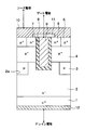
- FIG. 1 is a diagram showing a cross-sectional configuration of an SiC semiconductor device having a vertical MOSFET having a trench gate structure according to the first embodiment.
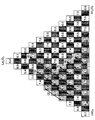
- FIG. 2 shows the result of obtaining C ⁇ Vb, ox [ ⁇ 10 ⁇ 6 C / cm 2 ] by changing each element content (atomic%) while using hafnium, aluminum and lanthanum as a constituent material of the gate insulating film.
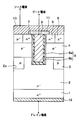
- FIG. 3 is a diagram showing a cross-sectional configuration of an SiC semiconductor device having a vertical MOSFET having a trench gate structure according to the second embodiment.
- FIG. 1 is a diagram showing a cross-sectional configuration of an SiC semiconductor device having a vertical MOSFET having a trench gate structure according to the first embodiment.
- FIG. 2 shows the result of obtaining C ⁇ Vb, ox [ ⁇ 10 ⁇ 6 C / cm 2 ] by changing each element content (atomic%) while using hafnium, aluminum and lanthanum as a constituent material of the gate
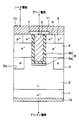
- FIG. 4 is a view showing a cross-sectional configuration of an SiC semiconductor device having a vertical MOSFET having a trench gate structure according to the third embodiment.
- FIG. 5 is a diagram showing a cross-sectional configuration of an SiC semiconductor device having a vertical MOSFET having a trench gate structure according to the fourth embodiment.
- FIG. 1 A first embodiment will be described.
- an SiC semiconductor device having a vertical MOSFET having an inverted trench gate structure shown in FIG. 1 will be described as an example of the SiC semiconductor device having a semiconductor element having a trench gate structure.
- FIG. 1 only one cell of the vertical MOSFET is shown, but a plurality of cells having the same structure as the vertical MOSFET shown in FIG. 1 are arranged adjacent to each other.
- the SiC semiconductor device includes an n-type impurity made of SiC single crystal doped with an n-type impurity such as phosphorus or nitrogen at a high concentration, for example, an impurity concentration of 1 ⁇ 10 19 to 1 ⁇ 10 20 cm ⁇ 3. It is formed using a + type semiconductor substrate 1. On the n + type semiconductor substrate 1, the thickness is lower than that of the n + type semiconductor substrate 1, and the n type impurity is doped with an impurity concentration of, for example, 1 ⁇ 10 15 to 1 ⁇ 10 16 cm ⁇ 3. An n-type drift layer 2 made of SiC having a thickness of about 5 to 15 ⁇ m is formed.
- the n-type drift layer 2 has a recess 2a that is partially recessed.
- the concave portion 2a is formed in a linear shape having a longitudinal direction in one direction, that is, a direction perpendicular to the paper surface of FIG. 1, and extends to a position deeper than a trench 7 constituting a trench gate structure to be described later, and in the same direction as the trench 7 Are formed in the longitudinal direction.
- an electric field relaxation layer 3 doped with a p-type impurity such as boron or aluminum is formed with the same direction as the longitudinal direction of the recess 2a being the longitudinal direction.
- the electric field relaxation layer 3 relaxes the gate electric field by suppressing the electric field from entering the bottom of the trench 7.
- the electric field relaxation layer 3 is about 1 ⁇ 10 17 to 1 ⁇ 10 19 cm ⁇ 3. It is formed to a deeper position.
- a p-type base region 4 is formed on the surfaces of the n-type drift layer 2 and the electric field relaxation layer 3.
- the p-type base region 4 is a layer constituting a channel of the vertical MOSFET, and is formed on both sides of a trench 7 constituting a trench gate structure described later so as to be in contact with the side surface of the trench 7.
- the n-type impurity is doped at a higher concentration than the n-type drift layer 2 so as to be in contact with the trench gate structure closer to the trench gate structure side than the position corresponding to the electric field relaxation layer 3 in the surface layer portion of the p-type base region 4.
- An n + -type source region 5 is formed.
- the n + -type source region 5 is formed with an impurity concentration of about 1 ⁇ 10 21 cm ⁇ 3 and a thickness of about 0.3 ⁇ m.
- a p-type impurity is heavily doped at a position corresponding to the electric field relaxation layer 3 in the surface layer portion of the p-type base region 4, that is, on the opposite side of the trench gate structure with the n + -type source region 5 interposed therebetween.
- a p + -type contact region 6 is formed.
- the p + -type contact region 6 is formed with an impurity concentration of about 1 ⁇ 10 21 cm ⁇ 3 and a thickness of about 0.3 ⁇ m.
- the n-type drift layer 2 is reached through the p-type base region 4 and the n + -type source region 5 at the center position of the electric field relaxation layers 3 arranged adjacent to each other, and A trench 7 which is shallower than the bottom of the relaxation layer 3 is formed.
- a p-type base region 4 and an n + -type source region 5 are arranged in contact with the side surface of the trench 7.
- the inner wall surface of the trench 7 is covered with a gate insulating film 8 made of a high dielectric constant film or the like.
- the inside of the trench 7 is filled with the gate electrode 9 made of doped Poly-Si formed on the surface of the gate insulating film 8.
- the trench gate structure is configured by the structure in which the gate insulating film 8 and the gate electrode 9 are provided in the trench 7.
- the gate insulating film 8 has a multilayer structure, and here, the gate insulating film 8 has a two-layer structure of a first layer 8a and a second layer 8b. Specifically, both the first layer 8a and the second layer 8b of the gate insulating film 8 are formed on the bottom and side walls of the trench 7, and the second layer 8b is formed of the first layer 8a. The structure is formed on the surface.
- the first layer 8a is composed of a silicon oxide film
- the second layer 8b is composed of the high dielectric constant film described in the first embodiment.
- the gate insulating film 8 has a multilayer structure, and the second layer 8b made of a high dielectric constant film is provided so as to cover the bottom of the trench 7, that is, at least the bottom of the gate electrode 9. ing.
- the trench gate structure has a strip shape, for example, with the vertical direction on the paper as the longitudinal direction, and a plurality of trench gate structures are arranged in stripes at equal intervals in the horizontal direction on the paper. As a result, the structure is provided with a plurality of cells.
- a source electrode 10 is formed on the surfaces of the n + type source region 5 and the p + type contact region 6.
- the source electrode 10 is composed of a plurality of metals (for example, nickel (Ni) and aluminum (Al)).
- the portion connected to n + type source region 5 is made of a metal capable of ohmic contact with n type SiC
- the portion connected to p type base region 4 via p + type contact region 6 is It is made of a metal capable of ohmic contact with p-type SiC.
- the source electrode 10 is electrically separated from a gate wiring (not shown) that is electrically connected to the gate electrode 9 via the interlayer insulating film 11.
- the source electrode 10 is in electrical contact with the n + type source region 5 and the p + type contact region 6 through a contact hole formed in the interlayer insulating film 11.
- n + -type semiconductor substrate 1 On the back side of the n + -type semiconductor substrate 1 n + -type semiconductor substrate 1 and electrically connected to the drain electrode 12 are formed. With such a structure, an n-channel type inverted MOSFET having a trench gate structure is formed.
- the second layer 8b formed of the high dielectric constant film in the gate insulating film 8 is formed of the trench 7 on the first layer 8a as described above. It is formed in all regions from the bottom to the side wall. Furthermore, in the case of the present embodiment, the second layer 8b is constituted by an amorphous film having an amorphous structure.
- the second layer 8b is made of a material having a dielectric constant higher than that of the silicon oxide film (SiO 2 ).
- the gate insulating film 8 has a capacitance per unit area as Cox and a dielectric breakdown voltage as Vb and ox.
- the gate insulating film of the element having the MOS structure When the gate insulating film of the element having the MOS structure is broken, an electric field higher than the breakdown voltage Vb, ox is applied to the gate insulating film.
- the dielectric breakdown electric field In the case where the gate insulating film is composed only of a commonly used silicon oxide film, the dielectric breakdown electric field is about 11 MV / cm. For this reason, for example, assuming that 1200 V is applied to the drain electrode when the device is turned off, when the gate insulating film of the device is broken, an electric field of 11 MV / cm or more is applied to the silicon oxide film at the broken portion. It will be.
- the gate insulating film 8 when a high dielectric constant film is used for part or all of the gate insulating film 8 and the capacitance is the same as that of the silicon oxide film and C ⁇ Vb, ox is doubled, the gate insulating film 8 The voltage that can be applied before breakdown can be doubled, and the margin when the same drain voltage is applied can be greatly increased.
- the second layer 8b of the gate insulating film 8 is a high dielectric constant film having the same composition in all regions from the bottom to the side wall of the trench 7.
- a portion in contact with the corner at the bottom of the substrate may be a high dielectric constant film.
- Examples of the high dielectric constant film constituting the second layer 8b include hafnium (Hf), aluminum (Al), lanthanum (La), cerium (Ce), zirconium (Zr), yttrium (Y), tantalum ( An insulating material containing one or more of Ta), strontium (Sr), and the like can be given.
- hafnium oxide (HfO 2 ) that is an insulating material containing hafnium
- aluminum oxide (Al 2 O 3 ) that is an insulating material containing aluminum
- lanthanum oxide (La 2 O 3 ) that is an insulating material containing lanthanum
- a dielectric constant film can be applied as the second layer 8b.
- a high dielectric constant film such as HfAlO, HfLaO, AlLaO, HfAlLaO containing hafnium and any one of aluminum or lanthanum can be applied as the second layer 8b.
- a high dielectric constant film containing any one of the above metal materials in addition to hafnium, aluminum and lanthanum can also be applied as the second layer 8b.
- FIG. 2 shows the experimental results.
- hafnium oxide, aluminum oxide, and lanthanum oxide formed on the silicon oxide film are used as constituent materials, and the contents of the constituent materials are changed.
- Each vertex of the triangle shown in FIG. 2 represents the case where the content rate of each constituent material is 100%, and indicates that the content rate of the constituent material increases or decreases by 10% every time one vertex is deviated from each vertex. ing.
- the upper vertex of the triangle is 100% lanthanum oxide
- the lower left vertex is 100% hafnium oxide
- the lower right vertex is 100% aluminum oxide.
- hafnium oxide is 90%.
- the content of aluminum oxide is 10%.
- the content rate of a constituent material here is represented as follows.
- the second layer 8b is constituted by a synthetic film in which, for example, aluminum oxide and hafnium oxide are mixed
- the content is x and the content of hafnium oxide is y in aluminum oxide
- the synthesis of aluminum oxide and hafnium oxide is performed.
- the aluminum oxide content is 0.1
- the hafnium oxide content is 0.25 to 0.75
- the lanthanum oxide content is 0.15 to 0.65.
- Cox ⁇ Vb, ox> 7.6 ⁇ 10 ⁇ 6 C / cm 2 was satisfied.
- the chemical formula is represented by (Al 2 O 3 ) 0.1 (HfO 2 ) 0.25 to 0.75 (La 2 O 3 ) 0.15 to 0.65 .
- the aluminum oxide content is 0.2
- the hafnium oxide content is 0.05 to 0.75
- the lanthanum oxide content is 0.05 to 0.75.
- Cox ⁇ Vb, ox> 7.6 ⁇ 10 ⁇ 6 C / cm 2 was satisfied.
- the chemical formula is represented by (Al 2 O 3 ) 0.2 (HfO 2 ) 0.05 to 0.75 (La 2 O 3 ) 0.05 to 0.75 .
- the aluminum oxide content is 0.3
- the hafnium oxide content is 0.35 to 0.55
- the lanthanum oxide content is 0.15 to 0.35.
- Cox ⁇ Vb, ox> 7.6 ⁇ 10 ⁇ 6 C / cm 2 was satisfied.
- the chemical formula is represented by (Al 2 O 3 ) 0.3 (HfO 2 ) 0.35 to 0.55 (La 2 O 3 ) 0.15 to 0.35 .
- the aluminum oxide content is 0.4
- the hafnium oxide content is 0.35 to 0.55
- the lanthanum oxide content is 0.05 to 0.25.
- Cox ⁇ Vb, ox> 7.6 ⁇ 10 ⁇ 6 C / cm 2 was satisfied.
- the chemical formula is represented by (Al 2 O 3 ) 0.4 (HfO 2 ) 0.35 to 0.55 (La 2 O 3 ) 0.05 to 0.25 .
- the aluminum oxide content is 0.5
- the hafnium oxide content is 0.35 to 0.45
- the lanthanum oxide content is 0.05 to 0.15.
- Cox ⁇ Vb, ox> 7.6 ⁇ 10 ⁇ 6 C / cm 2 was satisfied.
- the chemical formula is represented by (Al 2 O 3 ) 0.5 (HfO 2 ) 0.35 to 0.45 (La 2 O 3 ) 0.05 to 0.15 .
- the content ratio of the constituent materials shown in the respective regions (1) to (7) in FIG. 2 can satisfy Cox ⁇ Vb, ox> 7.6 ⁇ 10 ⁇ 6 C / cm 2 . Therefore, when the second layer 8b is formed using any two or more constituent materials of hafnium oxide, aluminum oxide, and lanthanum oxide, the content shown in at least the regions (1) to (7) is obtained. In some cases, a high breakdown voltage of the vertical MOSFET can be realized.
- hafnium oxide, aluminum oxide, and lanthanum oxide in the case where the second layer 8b is formed using hafnium oxide, aluminum oxide, and lanthanum oxide as constituent materials are shown. This is represented by the following element contents of hafnium, aluminum and lanthanum.
- element content rate here is calculated
- the second layer 8b is composed of a synthetic film of hafnium oxide and aluminum oxide, as described above, when the content rate is x and the content rate of aluminum oxide is y in hafnium oxide, hafnium oxide and The synthetic film with aluminum oxide is represented by the above chemical formula 1.
- the element content of hafnium is 1 ⁇ x
- the element content of aluminum is 2 ⁇ y
- the element content of oxygen is 2 ⁇ x + 3 ⁇ y.
- the chemical formula is: It becomes.
- the element content is 5 to 31% for hafnium and 3 to 34% for aluminum.
- region (2) that is, when the second layer 8b is composed of a high dielectric constant film containing hafnium and lanthanum, the element content is 10 to 22% for hafnium and 14 to 27% for lanthanum.
- the element content is 1 to 22% for hafnium and 4 to 4 for aluminum. 25% for lanthanum and 2 to 31%.
- the element content in each of the regions (1) to (7) in FIG. 2 is as described above.
- Cox ⁇ Vb, ox> 7.6 ⁇ 10 ⁇ 6 C / cm 2 can be satisfied, and the high breakdown voltage of the vertical MOSFET can be increased.
- the lanthanum content should be as small as possible.
- nitrogen (N) or hydrogen (H) can be included as a constituent material of the second layer 8b.
- the elemental content of nitrogen is set to 1 to 30%.
- the crystallization temperature of the second layer 8b can be increased, and the temperature applicable during the process can be increased, so that the degree of freedom in the process can be further increased.
- the elemental content of hydrogen is set to 1 to 10%.
- the entire region from the bottom of the trench 7 to the side wall of the second layer 8b of the gate insulating film 8 is a high dielectric constant film. It is composed by.
- the gate insulating film 8 is made of a material having a dielectric constant higher than that of the silicon oxide film (SiO 2 ) and satisfying the relationship of Cox ⁇ Vb, ox> 7.6 ⁇ 10 ⁇ 6 C / cm 2 or more. It is composed.
- the manufacturing method of the SiC semiconductor device having the vertical MOSFET according to the present embodiment is basically the same as the conventional manufacturing method, and the constituent material for forming the gate insulating film 8 is changed from the conventional one. Or changing the forming method.
- the gate insulating film 8 can be formed by the chemical vapor deposition (CVD) method, the atomic vapor deposition (ALD) method, or the like for both the first layer 8a and the second layer 8b.
- the first layer 8a may be formed by a thermal oxidation method or a deposition method.
- the atmosphere at the time of forming the second layer 8b is a nitrogen atmosphere or a hydrogen atmosphere, or the second layer 8b is in a state not containing nitrogen or hydrogen.
- Heat treatment may be performed in a nitrogen atmosphere or a hydrogen atmosphere after the formation of the two layers 8b.
- the gate insulating film 8 is configured by a single layer structure, and the gate insulating film 8 is formed on the bottom and side walls of the trench 7.
- the entire gate insulating film 8 is constituted by the high dielectric constant film constituting the second layer 8b described in the first embodiment.
- the material of the high dielectric constant film used as the gate insulating film 8 of the present embodiment is the same as the constituent material of the second layer 8b described in the first embodiment.
- the manufacturing method of the SiC semiconductor device having the vertical MOSFET having such a structure is basically the same as the conventional method, except that the formation process of the gate insulating film 8 is different.
- the gate insulating film 8 may be manufactured by using the method for forming the second layer 8b composed of the high dielectric constant film described in the first embodiment.
- the gate insulating film 8 may be formed of one kind of film over the entire surface of the bottom and side walls of the trench 7, so that the gate insulating film 8 can be easily formed.
- the first layer 8a is formed only on the side wall of the trench 7 and is not formed on the bottom.
- the second layer 8 a is in contact with the n-type drift layer 2 at the bottom of the trench 7.
- the second layer 8b made of a high dielectric constant film is provided so as to cover the bottom of the trench 7, that is, at least the bottom of the gate electrode 9, the first layer is provided.
- the first layer 8a is formed only on the side wall portion of the trench 7, it becomes possible to reduce the gate capacitance, and it is possible to reduce the switching loss of the vertical MOSFET.
- the manufacturing method of the SiC semiconductor device having the vertical MOSFET having such a structure is basically the same as that of the first embodiment. However, as a step of forming the gate insulating film 8, after the first layer 8a is formed, the second layer 8b is formed after removing the bottom portion of the trench 7 in the first layer 8a by anisotropic etching or the like. Will be performed.
- the first layer 8a is formed only on the bottom of the trench 7 and is not formed on the side wall.
- the second layer 8 a is in contact with the n-type drift layer 2 and the p-type base region 4 at the side wall of the trench 7.
- the second layer 8b made of a high dielectric constant film is provided so as to cover the bottom of the trench 7, that is, at least the bottom of the gate electrode 9, the first layer is provided.
- the first layer 8a is formed only at the bottom of the trench 7, it is possible to reduce the gate capacitance, and to reduce the switching loss of the vertical MOSFET.
- the manufacturing method of the SiC semiconductor device having the vertical MOSFET having such a structure is basically the same as that of the first embodiment. However, as the step of forming the gate insulating film 8, after the first layer 8a is formed, the second layer 8b is formed after the first layer 8a is left only at the bottom portion of the trench 7 by etch back. Will do.
- the structure of the gate insulating film 8 has been described with some examples. However, these are only examples, and a portion of the gate insulating film 8 located at the bottom of the trench 7, in other words, a portion of the gate electrode 9 located at least at the bottom of the trench 7 and The corresponding part should just be comprised with the high dielectric constant film
- an oxide film is cited as an example of an insulating material containing at least one of hafnium, aluminum, lanthanum, cerium, zirconium, yttrium, tantalum, strontium, and the like constituting the high dielectric constant film constituting the gate insulating film 8
- An oxynitride film may be used.
- the gate insulating film 8 can be composed of an amorphous film having an amorphous structure, but can also be composed of a crystal film having a crystal structure.
- amorphous structure since there is no crystal grain boundary, it becomes possible to suppress the leakage current.
- doping with zirconium, yttrium, or the like provides an effect that the crystallinity is changed and the relative dielectric constant can be further increased.
- an n-channel type MOSFET in which the first conductivity type is n-type and the second conductivity type is p-type has been described as an example.
- the present disclosure can be applied to a channel type MOSFET.
- a MOSFET having a trench gate structure has been described as an example, but the present disclosure can be applied to an IGBT having a similar trench gate structure.
- the IGBT only changes the conductivity type of the n + type substrate 1 from the n-type to the p-type with respect to the above-described embodiments, and the other structures and manufacturing methods are the same as those of the above-described embodiments.
Landscapes
- Electrodes Of Semiconductors (AREA)
Applications Claiming Priority (2)
| Application Number | Priority Date | Filing Date | Title |
|---|---|---|---|
| JP2015218815A JP2017092191A (ja) | 2015-11-06 | 2015-11-06 | 炭化珪素半導体装置 |
| JP2015-218815 | 2015-11-06 |
Publications (1)
| Publication Number | Publication Date |
|---|---|
| WO2017077780A1 true WO2017077780A1 (ja) | 2017-05-11 |
Family
ID=58661812
Family Applications (1)
| Application Number | Title | Priority Date | Filing Date |
|---|---|---|---|
| PCT/JP2016/077776 Ceased WO2017077780A1 (ja) | 2015-11-06 | 2016-09-21 | 炭化珪素半導体装置 |
Country Status (2)
| Country | Link |
|---|---|
| JP (1) | JP2017092191A (enExample) |
| WO (1) | WO2017077780A1 (enExample) |
Cited By (2)
| Publication number | Priority date | Publication date | Assignee | Title |
|---|---|---|---|---|
| CN107706230A (zh) * | 2017-09-28 | 2018-02-16 | 中国电子科技集团公司第五十五研究所 | 一种功率槽栅mos型器件及制备方法 |
| JP2019114724A (ja) * | 2017-12-25 | 2019-07-11 | 富士電機株式会社 | 半導体装置および半導体装置の製造方法 |
Families Citing this family (1)
| Publication number | Priority date | Publication date | Assignee | Title |
|---|---|---|---|---|
| WO2023058209A1 (en) * | 2021-10-07 | 2023-04-13 | Fuji Electric Co., Ltd. | Method of manufacturing silicon carbide semiconductor device |
Citations (5)
| Publication number | Priority date | Publication date | Assignee | Title |
|---|---|---|---|---|
| JP2004214366A (ja) * | 2002-12-27 | 2004-07-29 | Nec Electronics Corp | 半導体装置及びその製造方法 |
| JP2007194652A (ja) * | 2001-06-21 | 2007-08-02 | Matsushita Electric Ind Co Ltd | 半導体装置 |
| JP2008243994A (ja) * | 2007-03-26 | 2008-10-09 | Toshiba Corp | 半導体装置及びその製造方法 |
| WO2008139621A1 (ja) * | 2007-05-15 | 2008-11-20 | Canon Anelva Corporation | 半導体素子の製造方法 |
| JP2013201308A (ja) * | 2012-03-26 | 2013-10-03 | Toshiba Corp | 半導体装置及びその製造方法 |
Family Cites Families (2)
| Publication number | Priority date | Publication date | Assignee | Title |
|---|---|---|---|---|
| JP2008091556A (ja) * | 2006-09-29 | 2008-04-17 | Toshiba Corp | 半導体装置 |
| JP5314964B2 (ja) * | 2008-08-13 | 2013-10-16 | ルネサスエレクトロニクス株式会社 | 半導体装置の製造方法 |
-
2015
- 2015-11-06 JP JP2015218815A patent/JP2017092191A/ja active Pending
-
2016
- 2016-09-21 WO PCT/JP2016/077776 patent/WO2017077780A1/ja not_active Ceased
Patent Citations (5)
| Publication number | Priority date | Publication date | Assignee | Title |
|---|---|---|---|---|
| JP2007194652A (ja) * | 2001-06-21 | 2007-08-02 | Matsushita Electric Ind Co Ltd | 半導体装置 |
| JP2004214366A (ja) * | 2002-12-27 | 2004-07-29 | Nec Electronics Corp | 半導体装置及びその製造方法 |
| JP2008243994A (ja) * | 2007-03-26 | 2008-10-09 | Toshiba Corp | 半導体装置及びその製造方法 |
| WO2008139621A1 (ja) * | 2007-05-15 | 2008-11-20 | Canon Anelva Corporation | 半導体素子の製造方法 |
| JP2013201308A (ja) * | 2012-03-26 | 2013-10-03 | Toshiba Corp | 半導体装置及びその製造方法 |
Cited By (3)
| Publication number | Priority date | Publication date | Assignee | Title |
|---|---|---|---|---|
| CN107706230A (zh) * | 2017-09-28 | 2018-02-16 | 中国电子科技集团公司第五十五研究所 | 一种功率槽栅mos型器件及制备方法 |
| JP2019114724A (ja) * | 2017-12-25 | 2019-07-11 | 富士電機株式会社 | 半導体装置および半導体装置の製造方法 |
| JP7062946B2 (ja) | 2017-12-25 | 2022-05-09 | 富士電機株式会社 | 半導体装置および半導体装置の製造方法 |
Also Published As
| Publication number | Publication date |
|---|---|
| JP2017092191A (ja) | 2017-05-25 |
Similar Documents
| Publication | Publication Date | Title |
|---|---|---|
| US10074728B2 (en) | Semiconductor device | |
| US20180114845A1 (en) | Semiconductor device | |
| KR20250168114A (ko) | 강유전층을 포함하는 전자 소자 | |
| US10971621B2 (en) | Semiconductor device | |
| US10923568B2 (en) | Semiconductor device, inverter circuit, and vehicle | |
| US20160079375A1 (en) | Semiconductor device and method for manufacturing same | |
| CN101626033A (zh) | 屏蔽栅沟槽fet结构及其形成方法 | |
| US10840368B2 (en) | Semiconductor device | |
| CN107431093A (zh) | 半导体装置 | |
| US11715773B2 (en) | Semiconductor device | |
| JP2014110402A (ja) | 半導体装置 | |
| US20230231009A1 (en) | Power semiconductor device | |
| US12453162B2 (en) | Semiconductor devices and methods of manufacturing the same | |
| WO2017077780A1 (ja) | 炭化珪素半導体装置 | |
| CN104124269A (zh) | 半导体装置 | |
| US20240405092A1 (en) | Semiconductor device comprising a high-k gate dielectric multilayer laminate structure and a method for manufacturing thereof | |
| JP2023549110A (ja) | 炭化珪素半導体装置の製造方法 | |
| JP7381425B2 (ja) | 半導体装置及びその製造方法 | |
| JP6052065B2 (ja) | 半導体素装置および半導体装置の製造方法 | |
| US20090289307A1 (en) | Semiconductor device | |
| JP6945036B2 (ja) | 半導体装置 | |
| KR102399430B1 (ko) | 전력 반도체 소자 및 그 제조 방법 | |
| JP2018129558A (ja) | 半導体装置 | |
| JP6346341B2 (ja) | 半導体装置 | |
| JP2023015636A (ja) | 半導体装置 |
Legal Events
| Date | Code | Title | Description |
|---|---|---|---|
| 121 | Ep: the epo has been informed by wipo that ep was designated in this application |
Ref document number: 16861849 Country of ref document: EP Kind code of ref document: A1 |
|
| NENP | Non-entry into the national phase |
Ref country code: DE |
|
| 122 | Ep: pct application non-entry in european phase |
Ref document number: 16861849 Country of ref document: EP Kind code of ref document: A1 |