WO2017073334A1 - 固体撮像素子および固体撮像素子の製造方法、並びに電子機器 - Google Patents
固体撮像素子および固体撮像素子の製造方法、並びに電子機器 Download PDFInfo
- Publication number
- WO2017073334A1 WO2017073334A1 PCT/JP2016/080298 JP2016080298W WO2017073334A1 WO 2017073334 A1 WO2017073334 A1 WO 2017073334A1 JP 2016080298 W JP2016080298 W JP 2016080298W WO 2017073334 A1 WO2017073334 A1 WO 2017073334A1
- Authority
- WO
- WIPO (PCT)
- Prior art keywords
- photoelectric conversion
- solid
- impurity layer
- state imaging
- type impurity
- Prior art date
- Legal status (The legal status is an assumption and is not a legal conclusion. Google has not performed a legal analysis and makes no representation as to the accuracy of the status listed.)
- Ceased
Links
Images






Classifications
-
- H—ELECTRICITY
- H10—SEMICONDUCTOR DEVICES; ELECTRIC SOLID-STATE DEVICES NOT OTHERWISE PROVIDED FOR
- H10F—INORGANIC SEMICONDUCTOR DEVICES SENSITIVE TO INFRARED RADIATION, LIGHT, ELECTROMAGNETIC RADIATION OF SHORTER WAVELENGTH OR CORPUSCULAR RADIATION
- H10F39/00—Integrated devices, or assemblies of multiple devices, comprising at least one element covered by group H10F30/00, e.g. radiation detectors comprising photodiode arrays
- H10F39/80—Constructional details of image sensors
- H10F39/802—Geometry or disposition of elements in pixels, e.g. address-lines or gate electrodes
- H10F39/8023—Disposition of the elements in pixels, e.g. smaller elements in the centre of the imager compared to larger elements at the periphery
-
- H—ELECTRICITY
- H04—ELECTRIC COMMUNICATION TECHNIQUE
- H04N—PICTORIAL COMMUNICATION, e.g. TELEVISION
- H04N25/00—Circuitry of solid-state image sensors [SSIS]; Control thereof
- H04N25/60—Noise processing, e.g. detecting, correcting, reducing or removing noise
- H04N25/63—Noise processing, e.g. detecting, correcting, reducing or removing noise applied to dark current
-
- H—ELECTRICITY
- H04—ELECTRIC COMMUNICATION TECHNIQUE
- H04N—PICTORIAL COMMUNICATION, e.g. TELEVISION
- H04N25/00—Circuitry of solid-state image sensors [SSIS]; Control thereof
- H04N25/70—SSIS architectures; Circuits associated therewith
- H04N25/76—Addressed sensors, e.g. MOS or CMOS sensors
-
- H—ELECTRICITY
- H10—SEMICONDUCTOR DEVICES; ELECTRIC SOLID-STATE DEVICES NOT OTHERWISE PROVIDED FOR
- H10F—INORGANIC SEMICONDUCTOR DEVICES SENSITIVE TO INFRARED RADIATION, LIGHT, ELECTROMAGNETIC RADIATION OF SHORTER WAVELENGTH OR CORPUSCULAR RADIATION
- H10F39/00—Integrated devices, or assemblies of multiple devices, comprising at least one element covered by group H10F30/00, e.g. radiation detectors comprising photodiode arrays
- H10F39/011—Manufacture or treatment of image sensors covered by group H10F39/12
-
- H—ELECTRICITY
- H10—SEMICONDUCTOR DEVICES; ELECTRIC SOLID-STATE DEVICES NOT OTHERWISE PROVIDED FOR
- H10F—INORGANIC SEMICONDUCTOR DEVICES SENSITIVE TO INFRARED RADIATION, LIGHT, ELECTROMAGNETIC RADIATION OF SHORTER WAVELENGTH OR CORPUSCULAR RADIATION
- H10F39/00—Integrated devices, or assemblies of multiple devices, comprising at least one element covered by group H10F30/00, e.g. radiation detectors comprising photodiode arrays
- H10F39/011—Manufacture or treatment of image sensors covered by group H10F39/12
- H10F39/014—Manufacture or treatment of image sensors covered by group H10F39/12 of CMOS image sensors
-
- H—ELECTRICITY
- H10—SEMICONDUCTOR DEVICES; ELECTRIC SOLID-STATE DEVICES NOT OTHERWISE PROVIDED FOR
- H10F—INORGANIC SEMICONDUCTOR DEVICES SENSITIVE TO INFRARED RADIATION, LIGHT, ELECTROMAGNETIC RADIATION OF SHORTER WAVELENGTH OR CORPUSCULAR RADIATION
- H10F39/00—Integrated devices, or assemblies of multiple devices, comprising at least one element covered by group H10F30/00, e.g. radiation detectors comprising photodiode arrays
- H10F39/10—Integrated devices
- H10F39/12—Image sensors
-
- H—ELECTRICITY
- H10—SEMICONDUCTOR DEVICES; ELECTRIC SOLID-STATE DEVICES NOT OTHERWISE PROVIDED FOR
- H10F—INORGANIC SEMICONDUCTOR DEVICES SENSITIVE TO INFRARED RADIATION, LIGHT, ELECTROMAGNETIC RADIATION OF SHORTER WAVELENGTH OR CORPUSCULAR RADIATION
- H10F39/00—Integrated devices, or assemblies of multiple devices, comprising at least one element covered by group H10F30/00, e.g. radiation detectors comprising photodiode arrays
- H10F39/10—Integrated devices
- H10F39/12—Image sensors
- H10F39/18—Complementary metal-oxide-semiconductor [CMOS] image sensors; Photodiode array image sensors
-
- H—ELECTRICITY
- H10—SEMICONDUCTOR DEVICES; ELECTRIC SOLID-STATE DEVICES NOT OTHERWISE PROVIDED FOR
- H10F—INORGANIC SEMICONDUCTOR DEVICES SENSITIVE TO INFRARED RADIATION, LIGHT, ELECTROMAGNETIC RADIATION OF SHORTER WAVELENGTH OR CORPUSCULAR RADIATION
- H10F39/00—Integrated devices, or assemblies of multiple devices, comprising at least one element covered by group H10F30/00, e.g. radiation detectors comprising photodiode arrays
- H10F39/10—Integrated devices
- H10F39/12—Image sensors
- H10F39/191—Photoconductor image sensors
-
- H—ELECTRICITY
- H10—SEMICONDUCTOR DEVICES; ELECTRIC SOLID-STATE DEVICES NOT OTHERWISE PROVIDED FOR
- H10F—INORGANIC SEMICONDUCTOR DEVICES SENSITIVE TO INFRARED RADIATION, LIGHT, ELECTROMAGNETIC RADIATION OF SHORTER WAVELENGTH OR CORPUSCULAR RADIATION
- H10F39/00—Integrated devices, or assemblies of multiple devices, comprising at least one element covered by group H10F30/00, e.g. radiation detectors comprising photodiode arrays
- H10F39/10—Integrated devices
- H10F39/12—Image sensors
- H10F39/199—Back-illuminated image sensors
-
- H—ELECTRICITY
- H10—SEMICONDUCTOR DEVICES; ELECTRIC SOLID-STATE DEVICES NOT OTHERWISE PROVIDED FOR
- H10F—INORGANIC SEMICONDUCTOR DEVICES SENSITIVE TO INFRARED RADIATION, LIGHT, ELECTROMAGNETIC RADIATION OF SHORTER WAVELENGTH OR CORPUSCULAR RADIATION
- H10F39/00—Integrated devices, or assemblies of multiple devices, comprising at least one element covered by group H10F30/00, e.g. radiation detectors comprising photodiode arrays
- H10F39/80—Constructional details of image sensors
- H10F39/802—Geometry or disposition of elements in pixels, e.g. address-lines or gate electrodes
-
- H—ELECTRICITY
- H10—SEMICONDUCTOR DEVICES; ELECTRIC SOLID-STATE DEVICES NOT OTHERWISE PROVIDED FOR
- H10F—INORGANIC SEMICONDUCTOR DEVICES SENSITIVE TO INFRARED RADIATION, LIGHT, ELECTROMAGNETIC RADIATION OF SHORTER WAVELENGTH OR CORPUSCULAR RADIATION
- H10F39/00—Integrated devices, or assemblies of multiple devices, comprising at least one element covered by group H10F30/00, e.g. radiation detectors comprising photodiode arrays
- H10F39/80—Constructional details of image sensors
- H10F39/803—Pixels having integrated switching, control, storage or amplification elements
- H10F39/8037—Pixels having integrated switching, control, storage or amplification elements the integrated elements comprising a transistor
-
- H—ELECTRICITY
- H10—SEMICONDUCTOR DEVICES; ELECTRIC SOLID-STATE DEVICES NOT OTHERWISE PROVIDED FOR
- H10F—INORGANIC SEMICONDUCTOR DEVICES SENSITIVE TO INFRARED RADIATION, LIGHT, ELECTROMAGNETIC RADIATION OF SHORTER WAVELENGTH OR CORPUSCULAR RADIATION
- H10F39/00—Integrated devices, or assemblies of multiple devices, comprising at least one element covered by group H10F30/00, e.g. radiation detectors comprising photodiode arrays
- H10F39/80—Constructional details of image sensors
- H10F39/807—Pixel isolation structures
-
- H—ELECTRICITY
- H10—SEMICONDUCTOR DEVICES; ELECTRIC SOLID-STATE DEVICES NOT OTHERWISE PROVIDED FOR
- H10F—INORGANIC SEMICONDUCTOR DEVICES SENSITIVE TO INFRARED RADIATION, LIGHT, ELECTROMAGNETIC RADIATION OF SHORTER WAVELENGTH OR CORPUSCULAR RADIATION
- H10F39/00—Integrated devices, or assemblies of multiple devices, comprising at least one element covered by group H10F30/00, e.g. radiation detectors comprising photodiode arrays
- H10F39/80—Constructional details of image sensors
- H10F39/811—Interconnections
Definitions
- the present technology relates to a solid-state imaging device, a manufacturing method of the solid-state imaging device, and an electronic device, and in particular, in a FD storage type sensor,
- the present invention relates to a method for manufacturing a solid-state imaging device and an electronic apparatus.
- FD Floating : Diffusion
- FD and PD Photo Diode
- pixel transistors are separated by element isolation such as STI (Shallow Trench Isolation). If the RST and Drain voltage of the FD is set to a low voltage, the electric field with PWell and STI can be relaxed and junction leakage can be suppressed (for example, Patent Documents 1, 2).
- This diffusion leak is observed as h + dark current in the FD and as e- dark current in the PD section when the PD sections are adjacent.
- the present technology has been made in view of such a situation, and in particular, in an FD storage type sensor, it is possible to suppress both occurrence of junction leak and diffusion leak in the FD.
- a solid-state imaging device is generated by a photodiode that performs photoelectric conversion according to the amount of incident light, a photoelectric conversion film that performs photoelectric conversion according to the amount of incident light, and photoelectric conversion of the photoelectric conversion film.
- a diode and the diffusion layer are juxtaposed, and the impurity layer is a solid-state imaging device provided below the diffusion layer.
- the impurity layer may be provided at a concentration higher than a predetermined concentration below the diffusion layer.
- the impurity layer may be provided at a concentration higher than 2.00E + 15 / cm 2 below the diffusion layer.
- the impurity layer may be provided below the diffusion layer and with a predetermined gap between the impurity layer and the diffusion layer.
- the impurity layer may be provided below the diffusion layer with a predetermined substance interposed between the impurity layer and the diffusion layer.
- the predetermined substance may be composed of the impurity layer having the second polarity.
- a method for manufacturing a solid-state imaging device includes a photodiode that performs photoelectric conversion according to the amount of incident light, a photoelectric conversion film that performs photoelectric conversion according to the amount of incident light, and photoelectric conversion of the photoelectric conversion film.
- the photodiode and the diffusion layer are juxtaposed in the same substrate, and the impurity layer is a manufacturing method of a solid-state imaging device provided below the diffusion layer.
- An electronic device is generated by a photodiode that performs photoelectric conversion according to the amount of incident light, a photoelectric conversion film that performs photoelectric conversion according to the amount of incident light, and photoelectric conversion of the photoelectric conversion film.
- the photodiode performs photoelectric conversion according to the amount of incident light
- the photoelectric conversion film performs photoelectric conversion according to the amount of incident light to form the first photodiode.
- Charges generated by photoelectric conversion of the photoelectric conversion film are accumulated by a diffusion layer having a second polarity different from the polarity, and an impurity layer made of an impurity of the first polarity is provided.
- a photodiode and the diffusion layer are juxtaposed, and the impurity layer is provided below the diffusion layer.
- the FD storage type sensor in the FD storage type sensor, it is possible to suppress both occurrence of junction leak and diffusion leak in the FD.
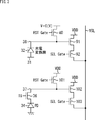
- FIG. 3 is a wiring diagram of the solid-state imaging device of FIG. 2.
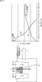
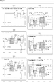
- FIG. 3 is a diagram showing a relationship between a P-type impurity concentration in a P-type impurity layer and a dark current flowing into PD in the solid-state imaging device of FIG. It is a figure explaining the distribution of the depth direction of FD and a P-type impurity layer. It is a flowchart explaining the manufacturing process of the solid-state image sensor of FIG. It is a figure explaining the manufacturing process of the solid-state image sensor of FIG.
- PD 1 photodiode 34 provided below (in the figure, above).
- PD photodiode 34
- the configurations of the solid-state imaging devices 11 in the upper and lower stages in FIG. 1 are basically the same, and when there is no need to distinguish between them, the respective configurations will be described without distinction. . In the following, the vertical relationship will be described based on the notation in the figure unless otherwise specified.
- the solid-state imaging device 11 in FIG. 1 is provided with a photoelectric conversion film 32 made of an organic film in the lower part of the drawing, and an upper electrode 31 in the solid-state imaging device 11 is provided thereunder. Yes.
- the photoelectric conversion film 32 generates a hole charge (indicated by “h +” in a circle in the drawing) according to the amount of incident light, and transfers the charge generated via the wiring 41 to the FD 38.
- a Pwell 33 made of a Si substrate is formed on the photoelectric conversion film 32.
- a photodiode (hereinafter also referred to as PD: Photo Diode) 34 is formed on the left side of the Pwell 33 in the drawing. More specifically, the PD 34 is composed of an N-type impurity layer (charge storage layer), and has a structure in which a high-concentration P-type impurity layer 35 forming a depletion prevention layer (pinning layer) is added to the PD 34. Yes.
- an FD 37 that is a diffusion layer for accumulating charges generated in the PD 34 is formed.
- a transfer gate (TG) 36 is formed in the left-right direction in the figure so as to straddle the P-type impurity layer 35 and the FD 37.
- the transfer gate 36 is controlled to be turned on, the charge accumulated in the PD 34 is transferred via the P-type impurity layer 35 to the FD 37 for the PD 34 made of a high-concentration N-type impurity layer.
- a shallow trench is formed and then sandwiched between STI (Shallow Trench Isolation) 39-1 and 39-2 formed by backfilling with an insulator made of an oxide film such as SiO2.
- the FD 38 is formed as a diffusion layer for the photoelectric conversion film 32 made of the high concentration N-type impurity layer 51 in the region.
- a wiring 41 that connects the photoelectric conversion film 32 and the FD 38 is connected to the source of a reset gate (RST Gate) 40.
- the PD 34 and the photoelectric conversion film 32 made of an organic film can be provided in the same substrate, and holes generated by photoelectric conversion in the photoelectric conversion film 32 according to the amount of incident light. Charges are transferred to the FD 38 and stored, and in the PD 34, charges generated by photoelectric conversion according to the amount of incident light are transferred to the FD 37 and stored. Further, when the reset gate (RST Gate) 40 is turned on, the charge transferred from the photoelectric conversion film 32 accumulated in the FD 38 is discharged.
- RST Gate reset gate
- the drain voltage of the reset gate 40 of the FD 38 is equal to the substrate potential.
- 0 [V] is set, a diffusion leak occurs from the FD 38.
- this diffusion leak is caused by the fact that the charge e ⁇ moves to the PD 34 as indicated by an arrow, thereby causing h + dark current in the FD 38 (“h +” in a circle in the figure). In the adjacent PD 34, it is observed as an e-dark current (indicated by a circle “e-”).
- the drain voltage of the reset gate 40 when the drain voltage of the reset gate 40 is set to a voltage slightly higher than the substrate potential (for example, about +0.3 [V]), the potential of the FD 38 is higher than that of the Pwell 33, so Is greatly suppressed, and the dark current of the PD 34 and the dark current of the FD 38 can be suppressed.
- the solid-state imaging device 11 of FIG. 2 differs from the solid-state imaging device 11 of FIG. 1 in the lower part of the N-type impurity layer 51 constituting the FD 38 that accumulates the charges generated by the photoelectric conversion film 32 in the figure.
- a P-type impurity layer 71 made of a high-concentration P-type impurity is provided.
- the P-type impurity layer 71 has a structure separated from the FD 38 that accumulates hole charges from the photoelectric conversion film 32 and the FD 37 that accumulates charges from the PD 34.
- the FD 38 is connected to the cathode side. Further, the FD 38 is connected to the source of the reset gate (RST Gate) 40 and the gate of the amplification transistor 91.
- a power supply VDD is applied between the source and drain of the amplification transistor 91, and the pixel signal is output after being amplified by a voltage corresponding to the electric charge stored in the FD 38, which is input to the gate.
- the selection gate (SEL Gate) 92 When the selection gate (SEL Gate) 92 is selected as a pixel instructed to transfer the pixel signal, the selection signal is input to the gate to be turned on, and when the selection signal is turned on, the selection gate (SEL ⁇ ⁇ ⁇ Gate) 92 The output is transferred via the vertical transfer line VSL.
- the transfer gate 36 is turned on when a transfer signal is input to the gate, and transfers the charge accumulated in the PD 34 to the FD 37.
- the FD 37 is connected to the source of the reset gate (RST Gate) 101 and the gate of the amplification transistor 102.
- the reset gate 101 is turned on when a reset signal is inputted from the gate, the power supply VDD connected to the drain side is turned on, and the electric charge accumulated in the FD 37 is discharged. At this time, if the transfer gate 36 is on, the charge accumulated in the PD 34 is also discharged.
- a power supply VDD is applied between the source and drain of the amplification transistor 102, and the pixel signal is output after being amplified by the voltage corresponding to the charge of the FD 37 input to the gate.
- the selection gate (SEL Gate) 103 When the selection gate (SEL Gate) 103 is selected as a pixel instructed to transfer the pixel signal, the selection gate 103 is turned on when the selection signal is input to the gate, and is turned on by the selection signal from the amplification transistor 102. Are transferred via the vertical transfer line VSL.
- the reset voltage V of the photoelectric conversion film 32 is set to 0 [V]
- the reset voltage of the PD 34 is set to the power supply voltage VDD.
- Diffusion leakage of the FD 38 occurs due to a minority carrier concentration gradient in the P-type impurity layer 71. For this reason, the higher the concentration of the P-type impurity layer 71 below the FD 38, the smaller the diffusion leak in the FD 38 and the dark current in the adjacent PD 34.
- the relationship between the dark current in the PD 34 and the P-type impurity concentration in the P-type impurity layer 71 below the FD 38 is as shown in FIG. 4 when calculated by the device simulator.
- P-type impurity concentration when the value exceeds 5.00E + 14 [/ cm 2 ], the PD dark current can be reduced to about 1/3, and at 2.00E + 15 [/ cm 2 ], the PD dark current can be reduced to 1/5 or less. Can be suppressed.
- the P-type impurity layer 71 is a lower layer portion of the N-type impurity layer 51 constituting the PD 38 and formed at a high concentration, diffusion leakage is suppressed.
- the reset voltage applied to the FD 38 can be set to 0 [V], which is the same as the substrate potential, the potential at the FD 38 in the dark is also close to 0 [V], so that the FD 38 and the Pwell 33 or between the FD 38 and the STI 39 The occurrence of a junction leak between ⁇ 1 and 39-2 can also be suppressed.
- the solid-state imaging device 11 in which the P-type impurity layer 71 is provided below the N-type impurity layer 51 forming the FD 38 as shown in FIG. Both diffusion leak and junction leak can be suppressed.
- the thicknesses of the N-type impurity layer 51 and the P-type impurity layer 71 in the FD 38 are, for example, as shown in the left part of FIG.
- the distribution is as shown on the right side of FIG.
- the horizontal axis indicates depth
- the vertical axis indicates the concentration of N-type impurities and P-type impurities in arbitrary units.
- N-type impurities have weaker acceleration energy in ion implantation than P-type impurities
- N-type impurity layer 51 is formed relatively thin.
- the P-type impurity requires a certain amount of I.I. energy in order to avoid interference with the P-type impurity. For this reason, the N-type impurity layer 51 is formed relatively thick with respect to the P-type impurity layer 71.
- step S11 as shown in the upper left part of FIG. 7, a trench made of a shallow groove is formed on a silicon wafer (Si wafer) constituting the Pwell 33, and then an insulator made of an oxide film such as SiO2 is buried. By returning, STI (Silicon Trench Isolation) 39-1 and 39-2 are formed. By a process described later, an FD 38 for accumulating charges generated by the photoelectric conversion film 32 is formed between the STIs 39-1 and 39-2.
- STI Silicon Trench Isolation
- step S12 as shown in the middle left part of FIG. 7, the PD 34, the P-type impurity layer 35, the N-type impurity layer 37, the N-type impurity layer 51 for forming the FD 38, and the P-type impurity layer 71 are formed by ion implantation. Is done.
- the components are formed in order from the configuration provided at the bottom of the drawing. Therefore, in the case of the left middle stage in FIG. 7, the P-type impurity layer 71, the PD 34, the P-type impurity layer 35, the N-type impurity layer 37, and the N-type impurity layer 51 are generally formed in this order.
- the P-type impurity layer 71 at a concentration higher than, for example, 5.00E + 14 [/ cm 2 ], it is possible to more reliably suppress junction leakage and diffusion leakage.
- step S13 as shown in the lower left part of FIG. 7, a transistor wiring 81 of the transfer gate 36 and a wiring 82 to the photoelectric conversion film 32 are formed.
- step S14 as shown in the upper right part of FIG. 7, the upper and lower sides are inverted, and the silicon wafer (Si wafer) side on which the upper Pwell 33 is formed is polished.
- step S15 as shown in the middle right part of FIG. 7, an electrode 41 that is a through electrode to the photoelectric conversion film 32 is formed on the silicon wafer (Si wafer) on which the Pwell 33 is formed, and is connected to the wiring 82.
- step S16 as shown in the lower right part of FIG. 7, a photoelectric conversion film 32 made of an organic film is formed on the upper surface of the silicon wafer (Si wafer) on which the Pwell 33 is formed, and the upper electrode 31 is further formed. As a result, the solid-state imaging device 11 is completed.
- the PD 34 and the photoelectric conversion film 32 are formed in the same substrate, and the N-type impurity layer 51 forming the FD 38 in which the charges generated by the photoelectric conversion film 32 are accumulated is formed. Since the P-type impurity layer 71 is configured, it is possible to suppress diffusion leak and junction leak in the FD 38.
- FIG. 8 shows a configuration example of the solid-state imaging device 11 in which the polarity of the solid-state imaging device 11 of FIG. 2 is reversed. That is, the solid-state imaging device 11 in FIG. 8 includes the photoelectric conversion film 32, the Pwell 33, the PD 34, the P-type impurity layer 35, the N-type impurity layer 37, the N-type impurity layer 51, and the P-type impurity in the solid-state imaging device 11 in FIG.
- a photoelectric conversion film 135, a Pwell 131, a PD 132, an N-type impurity layer 133, a P-type impurity layer 134, an FD 38 composed of a P-type impurity layer 151, and an N-type impurity layer 152 are provided. It has been.
- the PD 132 is formed of a P-type impurity layer, and the photoelectric conversion film 135 generates charges (indicated by “e +” in a circle in the drawing), and the wiring The data is transferred to the FD 38 via 41.
- the wiring diagram of FIG. 9 differs from the wiring diagram of FIG. 3 in that a photoelectric conversion film 135 and a PD 132 are provided instead of the photoelectric conversion film 32 and the PD 34, and the reset gate of the photoelectric conversion film 135 is provided.
- the manufacturing process of the solid-state image sensor 11 in FIG. 8 is a process for manufacturing a configuration corresponding to the solid-state image sensor 11 in FIG.
- FIG. 10 shows a configuration example of the solid-state imaging device 11 in which the P-type impurity layer 71 is provided at a deeper position than the N-type impurity layer 51.
- a space below the N-type impurity layer 51 constituting the FD 38 and not in contact with a predetermined distance is provided, and the P-type impurity layer is deeper than the N-type impurity layer 51.
- the N-type impurity layer 152 is provided deeply below the P-type impurity layer 151 constituting the FD 38.
- the P-type impurity layer 71 ′ is provided immediately below the N-type impurity layer 51 constituting the FD 38 and deeper than the N-type impurity layer 51.
- junction leakage is further reduced.
- an N-type impurity layer 171 may be further provided between the N-type impurity layer 51 and the P-type impurity layer 71 ′ in the deep part.
- FIG. 11 shows a configuration example of the solid-state imaging device 11 in which a low-concentration N-type impurity layer 171 is provided between the N-type impurity layer 51 and the P-type impurity layer 71 ′.
- the N-type impurity layer 171 between the N-type impurity layer 51 and the P-type impurity layer 71 ′ constituting the FD 38 by providing the N-type impurity layer 171 between the N-type impurity layer 51 and the P-type impurity layer 71 ′ constituting the FD 38, the P-type impurity layer 71 ′ near the FD 38 is provided. Since the electric field between the FD 38 and the P-type impurity layer 71 ′ is relaxed by the N-type impurity layer 171, junction leakage can be further reduced.
- an N-type impurity layer 152 is provided deeply below the P-type impurity layer 151 constituting the FD 38, and further the FD 38 is configured.
- a P-type impurity layer is provided between the P-type impurity layer 151 and the N-type impurity layer 152.
- the solid-state imaging device described above can be applied to various electronic devices such as an imaging device such as a digital still camera and a digital video camera, a mobile phone having an imaging function, or other devices having an imaging function. .
- FIG. 12 is a block diagram illustrating a configuration example of an imaging apparatus as an electronic apparatus to which the present technology is applied.
- An imaging apparatus 201 shown in FIG. 12 includes an optical system 202, a shutter device 203, a solid-state imaging device 204, a drive circuit 205, a signal processing circuit 206, a monitor 207, and a memory 208, and displays still images and moving images. Imaging is possible.
- the optical system 202 includes one or more lenses, guides light (incident light) from a subject to the solid-state image sensor 204, and forms an image on the light receiving surface of the solid-state image sensor 204.
- the shutter device 203 is disposed between the optical system 202 and the solid-state imaging device 204, and controls the light irradiation period and the light-shielding period to the solid-state imaging device 204 according to the control of the drive circuit 1005.
- the solid-state image sensor 204 is configured by a package including the solid-state image sensor 11 described above.
- the solid-state imaging device 204 accumulates signal charges for a certain period in accordance with light imaged on the light receiving surface via the optical system 202 and the shutter device 203.
- the signal charge accumulated in the solid-state image sensor 204 is transferred according to a drive signal (timing signal) supplied from the drive circuit 205.
- the drive circuit 205 outputs a drive signal for controlling the transfer operation of the solid-state image sensor 204 and the shutter operation of the shutter device 203 to drive the solid-state image sensor 204 and the shutter device 203.
- the signal processing circuit 206 performs various types of signal processing on the signal charges output from the solid-state imaging device 204.
- An image (image data) obtained by the signal processing by the signal processing circuit 206 is supplied to the monitor 207 and displayed, or supplied to the memory 208 and stored (recorded).
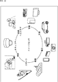
- FIG. 13 is a diagram showing a usage example in which the above-described solid-state imaging device is used.
- the solid-state imaging device described above can be used in various cases for sensing light such as visible light, infrared light, ultraviolet light, and X-ray as follows.
- Devices for taking images for viewing such as digital cameras and mobile devices with camera functions
- Devices used for traffic such as in-vehicle sensors that capture the back, surroundings, and interiors of vehicles, surveillance cameras that monitor traveling vehicles and roads, and ranging sensors that measure distances between vehicles, etc.
- Equipment used for home appliances such as TVs, refrigerators, air conditioners, etc. to take pictures and operate the equipment according to the gestures ⁇ Endoscopes, equipment that performs blood vessel photography by receiving infrared light, etc.
- Equipment used for medical and health care ⁇ Security equipment such as security surveillance cameras and personal authentication cameras ⁇ Skin measuring instrument for photographing skin and scalp photography Such as a microscope to do beauty Equipment used for sports-Equipment used for sports such as action cameras and wearable cameras for sports applications-Used for agriculture such as cameras for monitoring the condition of fields and crops apparatus
- this technique can also take the following structures.
- a photodiode that performs photoelectric conversion according to the amount of incident light;
- a photoelectric conversion film that performs photoelectric conversion according to the amount of incident light;
- a diffusion layer having a second polarity different from the first polarity for forming the photodiode, for accumulating charges generated by photoelectric conversion of the photoelectric conversion film;
- An impurity layer comprising the first polar impurity, The photodiode and the diffusion layer are juxtaposed in the same substrate, and the impurity layer is provided below the diffusion layer.
- ⁇ 2> The solid-state imaging device according to ⁇ 1>, wherein the impurity layer is provided at a lower concentration than a predetermined concentration below the diffusion layer.
- ⁇ 3> The solid-state imaging device according to ⁇ 2>, wherein the impurity layer is provided at a lower concentration than 2.00E + 15 / cm 2 below the diffusion layer.
- ⁇ 4> The solid-state imaging device according to any one of ⁇ 1> to ⁇ 3>, wherein the impurity layer is provided below the diffusion layer and at a predetermined interval from the diffusion layer.
- ⁇ 5> The solid-state imaging device according to any one of ⁇ 1> to ⁇ 3>, wherein the impurity layer is provided below the diffusion layer with a predetermined substance interposed between the impurity layer and the diffusion layer.
- the predetermined substance includes the impurity layer having the second polarity.
- a photodiode that performs photoelectric conversion according to the amount of incident light
- a photoelectric conversion film that performs photoelectric conversion according to the amount of incident light
- a diffusion layer having a second polarity different from the first polarity for forming the photodiode, for accumulating charges generated by photoelectric conversion of the photoelectric conversion film
- An impurity layer comprising the first polar impurity
- a photodiode that performs photoelectric conversion according to the amount of incident light
- a photoelectric conversion film that performs photoelectric conversion according to the amount of incident light
- a diffusion layer having a second polarity different from the first polarity for forming the photodiode, for accumulating charges generated by photoelectric conversion of the photoelectric conversion film
- An impurity layer comprising the first polar impurity
- 11 solid-state imaging device 31 upper wiring, 32 photoelectric conversion film, 33 Pwell, 34 PD, 35 P-type impurity layer, 36 transfer gate, 37 N-type impurity layer, 38 FD, 39-1, 39-2 STI, 40 reset Gate, 41 wiring, 51 N-type impurity layer, 71, 71 'P-type impurity layer, 91 amplification transistor, 92 selection gate, 101 reset gate, 102 amplification transistor, 103 selection gate, 131 Nwell, 132 PD, 133 N-type impurity Layer, 134 P-type impurity layer, 135 photoelectric conversion film, 151 P-type impurity layer, 152 N-type impurity layer, 171 N-type impurity layer
Landscapes
- Engineering & Computer Science (AREA)
- Multimedia (AREA)
- Signal Processing (AREA)
- Solid State Image Pick-Up Elements (AREA)
- Transforming Light Signals Into Electric Signals (AREA)
Abstract
Description
<従来の固体撮像素子の実施の形態の構成例>
本技術を適用した固体撮像素子の説明に当たって、図1の側面断面図を参照して、一般的な固体撮像素子の構成について説明する。
次に、図2の側面断面図を参照して、本技術を適用した固体撮像素子の構成例について説明する。尚、図2の固体撮像素子の構成において、図1の固体撮像素子の構成と同一の機能を備えた構成については、同一の名称、および同一の符号を付しており、その説明は適宜省略するものとする。
次に、図3の回路図を参照して、図2の固体撮像素子11の等価回路について説明する。
また、FD38におけるN型不純物層51とP型不純物層71の厚さは、例えば、図5の左部で示されるように、FD38におけるN型不純物層51およびP型不純物層71における図中の矢印で示される方向におけるN型不純物層51の図中上部を深さの基準としたときに、図5の右部で示されるような分布となる。尚、図5の左部は、横軸が深さ(depth)を示し、縦軸がN型不純物およびP型不純物の濃度を任意単位で示したものである。
次に、図6のフローチャート、および図7の製造処理を説明する図を参照して、図2の固体撮像素子11の製造処理について説明する。
以上においては、PD34が、N型不純物層により形成され、光電変換膜32が、ホール電荷を発生する例について説明してきたが、極性を反転したものを構成するようにしても、同様の効果を奏することが可能となる。
以上においては、図2の固体撮像素子11で示されるように、FD38を構成するN型不純物層51の直下にP型不純物層71が設けられる例について説明してきたが、P型不純物層71をN型不純物層51に対して、より深い位置に設けるようにしてもよい。
以上においては、図10の固体撮像素子11で示されるように、FD38を構成するN型不純物層51の直下であって、N型不純物層51より深部にP型不純物層71’が設けられるようにすることで、ジャンクションリークを、より低減させる例について説明してきた。
上述した固体撮像素子は、例えば、デジタルスチルカメラやデジタルビデオカメラなどの撮像装置、撮像機能を備えた携帯電話機、または、撮像機能を備えた他の機器といった各種の電子機器に適用することができる。
<固体撮像素子の使用例>
・自動停止等の安全運転や、運転者の状態の認識等のために、自動車の前方や後方、周囲、車内等を撮影する車載用センサ、走行車両や道路を監視する監視カメラ、車両間等の測距を行う測距センサ等の、交通の用に供される装置
・ユーザのジェスチャを撮影して、そのジェスチャに従った機器操作を行うために、TVや、冷蔵庫、エアーコンディショナ等の家電に供される装置
・内視鏡や、赤外光の受光による血管撮影を行う装置等の、医療やヘルスケアの用に供される装置
・防犯用途の監視カメラや、人物認証用途のカメラ等の、セキュリティの用に供される装置
・肌を撮影する肌測定器や、頭皮を撮影するマイクロスコープ等の、美容の用に供される装置
・スポーツ用途等向けのアクションカメラやウェアラブルカメラ等の、スポーツの用に供される装置
・畑や作物の状態を監視するためのカメラ等の、農業の用に供される装置
<1> 入射光の光量に応じて光電変換するフォトダイオードと、
入射光の光量に応じて光電変換する光電変換膜と、
前記光電変換膜の光電変換により発生された電荷を蓄積する、前記フォトダイオードを形成する第1の極性と異なる第2の極性からなる拡散層と、
前記第1の極性の不純物からなる不純物層とを含み、
同一基板内に、前記フォトダイオードと前記拡散層とが並置されており、前記不純物層が、前記拡散層の下部に設けられる
固体撮像素子。
<2> 前記不純物層は、前記拡散層の下部に所定の濃度よりも高濃度に設けられる
<1>に記載の固体撮像素子。
<3> 前記不純物層は、前記拡散層の下部に2.00E+15/cm2よりも高濃度に設けられる
<2>に記載の固体撮像素子。
<4> 前記不純物層は、前記拡散層の下部であって、前記拡散層との間に所定の間隔をおいて設けられる
<1>乃至<3>のいずれかに記載の固体撮像素子。
<5> 前記不純物層は、前記拡散層の下部であって、前記拡散層との間に所定の物質を挟んで設けられる
<1>乃至<3>のいずれかに記載の固体撮像素子。
<6> 前記所定の物質は、前記第2の極性の不純物層からなる
<1>に記載の固体撮像素子。
<7> 入射光の光量に応じて光電変換するフォトダイオードと、
入射光の光量に応じて光電変換する光電変換膜と、
前記光電変換膜の光電変換により発生された電荷を蓄積する、前記フォトダイオードを形成する第1の極性と異なる第2の極性からなる拡散層と、
前記第1の極性の不純物からなる不純物層とを含み、
固体撮像素子の製造方法であって、
同一基板内に、前記フォトダイオードと前記拡散層とが並置されており、前記不純物層が、前記拡散層の下部に設けられる
固体撮像素子の製造方法。
<8> 入射光の光量に応じて光電変換するフォトダイオードと、
入射光の光量に応じて光電変換する光電変換膜と、
前記光電変換膜の光電変換により発生された電荷を蓄積する、前記フォトダイオードを形成する第1の極性と異なる第2の極性からなる拡散層と、
前記第1の極性の不純物からなる不純物層とを含み、
同一基板内に、前記フォトダイオードと前記拡散層とが並置されており、前記不純物層が、前記拡散層の下部に設けられる
電子機器。
Claims (8)
- 入射光の光量に応じて光電変換するフォトダイオードと、
入射光の光量に応じて光電変換する光電変換膜と、
前記光電変換膜の光電変換により発生された電荷を蓄積する、前記フォトダイオードを形成する第1の極性と異なる第2の極性からなる拡散層と、
前記第1の極性の不純物からなる不純物層とを含み、
同一基板内に、前記フォトダイオードと前記拡散層とが並置されており、前記不純物層が、前記拡散層の下部に設けられる
固体撮像素子。 - 前記不純物層は、前記拡散層の下部に所定の濃度よりも高濃度に設けられる
請求項1に記載の固体撮像素子。 - 前記不純物層は、前記拡散層の下部に2.00E+15/cm2よりも高濃度に設けられる
請求項2に記載の固体撮像素子。 - 前記不純物層は、前記拡散層の下部であって、前記拡散層との間に所定の間隔をおいて設けられる
請求項1に記載の固体撮像素子。 - 前記不純物層は、前記拡散層の下部であって、前記拡散層との間に所定の物質を挟んで設けられる
請求項1に記載の固体撮像素子。 - 前記所定の物質は、前記第2の極性の不純物層からなる
請求項1に記載の固体撮像素子。 - 入射光の光量に応じて光電変換するフォトダイオードと、
入射光の光量に応じて光電変換する光電変換膜と、
前記光電変換膜の光電変換により発生された電荷を蓄積する、前記フォトダイオードを形成する第1の極性と異なる第2の極性からなる拡散層と、
前記第1の極性の不純物からなる不純物層とを含み、
固体撮像素子の製造方法であって、
同一基板内に、前記フォトダイオードと前記拡散層とが並置されており、前記不純物層が、前記拡散層の下部に設けられる
固体撮像素子の製造方法。 - 入射光の光量に応じて光電変換するフォトダイオードと、
入射光の光量に応じて光電変換する光電変換膜と、
前記光電変換膜の光電変換により発生された電荷を蓄積する、前記フォトダイオードを形成する第1の極性と異なる第2の極性からなる拡散層と、
前記第1の極性の不純物からなる不純物層とを含み、
同一基板内に、前記フォトダイオードと前記拡散層とが並置されており、前記不純物層が、前記拡散層の下部に設けられる
電子機器。
Priority Applications (3)
| Application Number | Priority Date | Filing Date | Title |
|---|---|---|---|
| JP2017547723A JP7126826B2 (ja) | 2015-10-27 | 2016-10-13 | 固体撮像素子および固体撮像素子の製造方法、並びに電子機器 |
| CN201680060919.7A CN108140662B (zh) | 2015-10-27 | 2016-10-13 | 固体摄像元件、固体摄像元件制造方法和电子设备 |
| US15/768,732 US10396108B2 (en) | 2015-10-27 | 2016-10-13 | Solid-state imaging element, solid-state imaging element manufacturing method, and electronic apparatus |
Applications Claiming Priority (2)
| Application Number | Priority Date | Filing Date | Title |
|---|---|---|---|
| JP2015210941 | 2015-10-27 | ||
| JP2015-210941 | 2015-10-27 |
Publications (1)
| Publication Number | Publication Date |
|---|---|
| WO2017073334A1 true WO2017073334A1 (ja) | 2017-05-04 |
Family
ID=58630323
Family Applications (1)
| Application Number | Title | Priority Date | Filing Date |
|---|---|---|---|
| PCT/JP2016/080298 Ceased WO2017073334A1 (ja) | 2015-10-27 | 2016-10-13 | 固体撮像素子および固体撮像素子の製造方法、並びに電子機器 |
Country Status (4)
| Country | Link |
|---|---|
| US (1) | US10396108B2 (ja) |
| JP (1) | JP7126826B2 (ja) |
| CN (1) | CN108140662B (ja) |
| WO (1) | WO2017073334A1 (ja) |
Cited By (1)
| Publication number | Priority date | Publication date | Assignee | Title |
|---|---|---|---|---|
| WO2025142948A1 (ja) * | 2023-12-25 | 2025-07-03 | ソニーセミコンダクタソリューションズ株式会社 | 光検出装置及び電子機器 |
Families Citing this family (2)
| Publication number | Priority date | Publication date | Assignee | Title |
|---|---|---|---|---|
| US11309348B2 (en) * | 2019-09-11 | 2022-04-19 | Taiwan Semiconductor Manufacturing Company, Ltd. | High density image sensor |
| CN110797368A (zh) * | 2019-12-10 | 2020-02-14 | 上海微阱电子科技有限公司 | 图像传感器单元及其制备方法 |
Citations (7)
| Publication number | Priority date | Publication date | Assignee | Title |
|---|---|---|---|---|
| JP2002016242A (ja) * | 2000-06-28 | 2002-01-18 | Toshiba Corp | Mos型固体撮像装置及びその製造方法 |
| JP2004193547A (ja) * | 2002-06-27 | 2004-07-08 | Canon Inc | 固体撮像装置及び固体撮像装置を用いたカメラシステム |
| JP2007273945A (ja) * | 2006-03-06 | 2007-10-18 | Fujifilm Corp | 光電変換素子及び固体撮像素子 |
| US20090250733A1 (en) * | 2008-04-08 | 2009-10-08 | International Business Machines Corporation | Pixel sensor with reduced image lag |
| JP2011082426A (ja) * | 2009-10-09 | 2011-04-21 | Canon Inc | 固体撮像装置 |
| WO2013021577A1 (ja) * | 2011-08-08 | 2013-02-14 | パナソニック株式会社 | 固体撮像装置及び固体撮像装置の駆動方法 |
| JP2015053296A (ja) * | 2013-01-28 | 2015-03-19 | ソニー株式会社 | 半導体素子およびこれを備えた半導体装置 |
Family Cites Families (7)
| Publication number | Priority date | Publication date | Assignee | Title |
|---|---|---|---|---|
| US7659973B2 (en) | 2006-05-26 | 2010-02-09 | Applied Materials Southeast Asia, Pte Ltd. | Wafer inspection using short-pulsed continuous broadband illumination |
| JP2011049524A (ja) * | 2009-07-27 | 2011-03-10 | Sony Corp | 固体撮像素子および固体撮像素子の製造方法 |
| CN103620783B (zh) * | 2011-06-23 | 2016-08-17 | 松下电器产业株式会社 | 固体摄像装置 |
| US9570489B2 (en) * | 2011-07-12 | 2017-02-14 | Sony Corporation | Solid state imaging device having impurity concentration on light receiving surface being greater or equal to that on opposing surface |
| JP2014060199A (ja) * | 2012-09-14 | 2014-04-03 | Toshiba Corp | 固体撮像装置の製造方法及び固体撮像装置 |
| JP6079502B2 (ja) * | 2013-08-19 | 2017-02-15 | ソニー株式会社 | 固体撮像素子および電子機器 |
| JP6725231B2 (ja) * | 2015-10-06 | 2020-07-15 | ソニーセミコンダクタソリューションズ株式会社 | 固体撮像素子、および電子装置 |
-
2016
- 2016-10-13 US US15/768,732 patent/US10396108B2/en active Active
- 2016-10-13 WO PCT/JP2016/080298 patent/WO2017073334A1/ja not_active Ceased
- 2016-10-13 JP JP2017547723A patent/JP7126826B2/ja active Active
- 2016-10-13 CN CN201680060919.7A patent/CN108140662B/zh active Active
Patent Citations (7)
| Publication number | Priority date | Publication date | Assignee | Title |
|---|---|---|---|---|
| JP2002016242A (ja) * | 2000-06-28 | 2002-01-18 | Toshiba Corp | Mos型固体撮像装置及びその製造方法 |
| JP2004193547A (ja) * | 2002-06-27 | 2004-07-08 | Canon Inc | 固体撮像装置及び固体撮像装置を用いたカメラシステム |
| JP2007273945A (ja) * | 2006-03-06 | 2007-10-18 | Fujifilm Corp | 光電変換素子及び固体撮像素子 |
| US20090250733A1 (en) * | 2008-04-08 | 2009-10-08 | International Business Machines Corporation | Pixel sensor with reduced image lag |
| JP2011082426A (ja) * | 2009-10-09 | 2011-04-21 | Canon Inc | 固体撮像装置 |
| WO2013021577A1 (ja) * | 2011-08-08 | 2013-02-14 | パナソニック株式会社 | 固体撮像装置及び固体撮像装置の駆動方法 |
| JP2015053296A (ja) * | 2013-01-28 | 2015-03-19 | ソニー株式会社 | 半導体素子およびこれを備えた半導体装置 |
Cited By (1)
| Publication number | Priority date | Publication date | Assignee | Title |
|---|---|---|---|---|
| WO2025142948A1 (ja) * | 2023-12-25 | 2025-07-03 | ソニーセミコンダクタソリューションズ株式会社 | 光検出装置及び電子機器 |
Also Published As
| Publication number | Publication date |
|---|---|
| US10396108B2 (en) | 2019-08-27 |
| CN108140662A (zh) | 2018-06-08 |
| US20180315787A1 (en) | 2018-11-01 |
| CN108140662B (zh) | 2023-01-17 |
| JP7126826B2 (ja) | 2022-08-29 |
| JPWO2017073334A1 (ja) | 2018-08-16 |
Similar Documents
| Publication | Publication Date | Title |
|---|---|---|
| US20200092505A1 (en) | Solid-state image sensor, driving method, and electronic apparatus | |
| US10692904B2 (en) | Solid-state image sensing device, drive method, and electronic apparatus | |
| JP2017183636A (ja) | 固体撮像素子、センサ装置、および電子機器 | |
| JP7622774B2 (ja) | 光検出素子、および電子装置 | |
| JP2016162917A (ja) | 固体撮像素子および電子機器 | |
| WO2019181555A1 (ja) | 撮像素子及び電子機器 | |
| US10741655B2 (en) | Semiconductor device, manufacturing method of the same, solid-state imaging device, and electronic device | |
| JP7126826B2 (ja) | 固体撮像素子および固体撮像素子の製造方法、並びに電子機器 | |
| WO2021193084A1 (ja) | 固体撮像装置、及び、固体撮像装置の製造方法 | |
| WO2017090455A1 (ja) | 半導体装置、製造方法 |
Legal Events
| Date | Code | Title | Description |
|---|---|---|---|
| 121 | Ep: the epo has been informed by wipo that ep was designated in this application |
Ref document number: 16859569 Country of ref document: EP Kind code of ref document: A1 |
|
| ENP | Entry into the national phase |
Ref document number: 2017547723 Country of ref document: JP Kind code of ref document: A |
|
| WWE | Wipo information: entry into national phase |
Ref document number: 15768732 Country of ref document: US |
|
| NENP | Non-entry into the national phase |
Ref country code: DE |
|
| 122 | Ep: pct application non-entry in european phase |
Ref document number: 16859569 Country of ref document: EP Kind code of ref document: A1 |